WO2022102480A1 - 回路モジュール及び大型回路システム - Google Patents
回路モジュール及び大型回路システム Download PDFInfo
- Publication number
- WO2022102480A1 WO2022102480A1 PCT/JP2021/040473 JP2021040473W WO2022102480A1 WO 2022102480 A1 WO2022102480 A1 WO 2022102480A1 JP 2021040473 W JP2021040473 W JP 2021040473W WO 2022102480 A1 WO2022102480 A1 WO 2022102480A1
- Authority
- WO
- WIPO (PCT)
- Prior art keywords
- circuit
- circuit module
- board
- circuit board
- board side
- Prior art date
- Legal status (The legal status is an assumption and is not a legal conclusion. Google has not performed a legal analysis and makes no representation as to the accuracy of the status listed.)
- Ceased
Links
Images




Classifications
-
- H—ELECTRICITY
- H05—ELECTRIC TECHNIQUES NOT OTHERWISE PROVIDED FOR
- H05K—PRINTED CIRCUITS; CASINGS OR CONSTRUCTIONAL DETAILS OF ELECTRIC APPARATUS; MANUFACTURE OF ASSEMBLAGES OF ELECTRICAL COMPONENTS
- H05K1/00—Printed circuits
- H05K1/02—Details
- H05K1/14—Structural association of two or more printed circuits
-
- H—ELECTRICITY
- H02—GENERATION; CONVERSION OR DISTRIBUTION OF ELECTRIC POWER
- H02M—APPARATUS FOR CONVERSION BETWEEN AC AND AC, BETWEEN AC AND DC, OR BETWEEN DC AND DC, AND FOR USE WITH MAINS OR SIMILAR POWER SUPPLY SYSTEMS; CONVERSION OF DC OR AC INPUT POWER INTO SURGE OUTPUT POWER; CONTROL OR REGULATION THEREOF
- H02M3/00—Conversion of DC power input into DC power output
- H02M3/02—Conversion of DC power input into DC power output without intermediate conversion into AC
- H02M3/04—Conversion of DC power input into DC power output without intermediate conversion into AC by static converters
- H02M3/10—Conversion of DC power input into DC power output without intermediate conversion into AC by static converters using discharge tubes with control electrode or semiconductor devices with control electrode
- H02M3/145—Conversion of DC power input into DC power output without intermediate conversion into AC by static converters using discharge tubes with control electrode or semiconductor devices with control electrode using devices of a triode or transistor type requiring continuous application of a control signal
- H02M3/155—Conversion of DC power input into DC power output without intermediate conversion into AC by static converters using discharge tubes with control electrode or semiconductor devices with control electrode using devices of a triode or transistor type requiring continuous application of a control signal using semiconductor devices only
- H02M3/156—Conversion of DC power input into DC power output without intermediate conversion into AC by static converters using discharge tubes with control electrode or semiconductor devices with control electrode using devices of a triode or transistor type requiring continuous application of a control signal using semiconductor devices only with automatic control of output voltage or current, e.g. switching regulators
- H02M3/158—Conversion of DC power input into DC power output without intermediate conversion into AC by static converters using discharge tubes with control electrode or semiconductor devices with control electrode using devices of a triode or transistor type requiring continuous application of a control signal using semiconductor devices only with automatic control of output voltage or current, e.g. switching regulators including plural semiconductor devices as final control devices for a single load
- H02M3/1584—Conversion of DC power input into DC power output without intermediate conversion into AC by static converters using discharge tubes with control electrode or semiconductor devices with control electrode using devices of a triode or transistor type requiring continuous application of a control signal using semiconductor devices only with automatic control of output voltage or current, e.g. switching regulators including plural semiconductor devices as final control devices for a single load with a plurality of power processing stages connected in parallel
- H02M3/1586—Conversion of DC power input into DC power output without intermediate conversion into AC by static converters using discharge tubes with control electrode or semiconductor devices with control electrode using devices of a triode or transistor type requiring continuous application of a control signal using semiconductor devices only with automatic control of output voltage or current, e.g. switching regulators including plural semiconductor devices as final control devices for a single load with a plurality of power processing stages connected in parallel switched with a phase shift, i.e. interleaved
-
- H—ELECTRICITY
- H02—GENERATION; CONVERSION OR DISTRIBUTION OF ELECTRIC POWER
- H02M—APPARATUS FOR CONVERSION BETWEEN AC AND AC, BETWEEN AC AND DC, OR BETWEEN DC AND DC, AND FOR USE WITH MAINS OR SIMILAR POWER SUPPLY SYSTEMS; CONVERSION OF DC OR AC INPUT POWER INTO SURGE OUTPUT POWER; CONTROL OR REGULATION THEREOF
- H02M3/00—Conversion of DC power input into DC power output
- H02M3/003—Constructional details, e.g. physical layout, assembly, wiring or busbar connections
-
- H—ELECTRICITY
- H05—ELECTRIC TECHNIQUES NOT OTHERWISE PROVIDED FOR
- H05K—PRINTED CIRCUITS; CASINGS OR CONSTRUCTIONAL DETAILS OF ELECTRIC APPARATUS; MANUFACTURE OF ASSEMBLAGES OF ELECTRICAL COMPONENTS
- H05K1/00—Printed circuits
- H05K1/02—Details
- H05K1/0201—Thermal arrangements, e.g. for cooling, heating or preventing overheating
- H05K1/0203—Cooling of mounted components
- H05K1/0209—External configuration of printed circuit board adapted for heat dissipation, e.g. lay-out of conductors, coatings
-
- H—ELECTRICITY
- H05—ELECTRIC TECHNIQUES NOT OTHERWISE PROVIDED FOR
- H05K—PRINTED CIRCUITS; CASINGS OR CONSTRUCTIONAL DETAILS OF ELECTRIC APPARATUS; MANUFACTURE OF ASSEMBLAGES OF ELECTRICAL COMPONENTS
- H05K1/00—Printed circuits
- H05K1/18—Printed circuits structurally associated with non-printed electric components
- H05K1/181—Printed circuits structurally associated with non-printed electric components associated with surface mounted components
-
- H—ELECTRICITY
- H05—ELECTRIC TECHNIQUES NOT OTHERWISE PROVIDED FOR
- H05K—PRINTED CIRCUITS; CASINGS OR CONSTRUCTIONAL DETAILS OF ELECTRIC APPARATUS; MANUFACTURE OF ASSEMBLAGES OF ELECTRICAL COMPONENTS
- H05K3/00—Apparatus or processes for manufacturing printed circuits
- H05K3/36—Assembling printed circuits with other printed circuits
- H05K3/368—Assembling printed circuits with other printed circuits parallel to each other
-
- H—ELECTRICITY
- H05—ELECTRIC TECHNIQUES NOT OTHERWISE PROVIDED FOR
- H05K—PRINTED CIRCUITS; CASINGS OR CONSTRUCTIONAL DETAILS OF ELECTRIC APPARATUS; MANUFACTURE OF ASSEMBLAGES OF ELECTRICAL COMPONENTS
- H05K1/00—Printed circuits
- H05K1/02—Details
- H05K1/14—Structural association of two or more printed circuits
- H05K1/144—Stacked arrangements of planar printed circuit boards
-
- H—ELECTRICITY
- H05—ELECTRIC TECHNIQUES NOT OTHERWISE PROVIDED FOR
- H05K—PRINTED CIRCUITS; CASINGS OR CONSTRUCTIONAL DETAILS OF ELECTRIC APPARATUS; MANUFACTURE OF ASSEMBLAGES OF ELECTRICAL COMPONENTS
- H05K2201/00—Indexing scheme relating to printed circuits covered by H05K1/00
- H05K2201/04—Assemblies of printed circuits
- H05K2201/042—Stacked spaced PCBs; Planar parts of folded flexible circuits having mounted components in between or spaced from each other
-
- H—ELECTRICITY
- H05—ELECTRIC TECHNIQUES NOT OTHERWISE PROVIDED FOR
- H05K—PRINTED CIRCUITS; CASINGS OR CONSTRUCTIONAL DETAILS OF ELECTRIC APPARATUS; MANUFACTURE OF ASSEMBLAGES OF ELECTRICAL COMPONENTS
- H05K2201/00—Indexing scheme relating to printed circuits covered by H05K1/00
- H05K2201/04—Assemblies of printed circuits
- H05K2201/044—Details of backplane or midplane for mounting orthogonal PCBs
-
- H—ELECTRICITY
- H05—ELECTRIC TECHNIQUES NOT OTHERWISE PROVIDED FOR
- H05K—PRINTED CIRCUITS; CASINGS OR CONSTRUCTIONAL DETAILS OF ELECTRIC APPARATUS; MANUFACTURE OF ASSEMBLAGES OF ELECTRICAL COMPONENTS
- H05K2201/00—Indexing scheme relating to printed circuits covered by H05K1/00
- H05K2201/10—Details of components or other objects attached to or integrated in a printed circuit board
- H05K2201/10007—Types of components
- H05K2201/10166—Transistor
Definitions
- the present invention relates to a circuit module board attached to a large circuit board, and more particularly to a circuit module board attached to a large circuit board without using solder and a large circuit system including the same.
- Patent Document 1 regarding an electronic module composed of a circuit board and electronic components mounted on the circuit board, a heat dissipation plate is arranged to face the lower surface of the circuit board, and the lower surface of the winding component and the circuit board An electronic module filled with a thermal conductor between the top surface and the top surface is shown.
- the module board When a circuit module including a module board is mounted on the back surface of a large circuit board, for example, the module board is generally temporarily fixed to the large board with an adhesive or the like to prevent the module board from falling. Soldering is performed by passing through a reflow furnace.
- a method of avoiding remelting of solder during reflow of a large circuit board by mounting various components constituting a circuit module using high melting point solder is conceivable, but the heat resistance of the components is limited and the solder options are limited. Therefore, it is difficult in reality.
- connection method instead of solder, there is a connection method using a conductive paste containing a metal filler such as silver paste.
- a material containing a large amount of metal filler may be used, but there is a limit because the adhesive strength is weakened. That is, there is a trade-off relationship between conductivity and adhesive strength.
- an object of the present invention is to realize high reliability and excellent electrical characteristics in a large circuit system in which a circuit module is mounted on a large circuit board without using soldering.
- the circuit module as an example of the present disclosure is mounted on a large circuit board having a fitting structure portion on the large circuit board side, and has a circuit module board having a smaller area than the large circuit board and an electronic circuit mounted on the circuit module board. It includes a component, a plurality of circuit module board side connection terminals provided on the circuit module board, and a circuit module board side fitting structure portion provided on the circuit module board.
- the plurality of circuit module board-side connection terminals include an electric signal terminal constituting an electric signal path and a large current terminal constituting a large current path of an electric power system, and are provided on the large circuit board.
- the large circuit board side connection terminal and the plurality of circuit module board side connection terminals are electrically connected, and the circuit module board side fitting structure portion and the large circuit board side fitting structure portion are electrically connected. Moreover, it is mechanically fixed, and is electrically insulated by a non-conductive heat conductive material between the facing surfaces of the circuit module board and the base material of the large circuit board, and is thermally bonded. It is characterized in that a layer is formed.
- the large circuit system of the present disclosure is composed of the above circuit module and a large circuit board on which the circuit module is mounted.
- FIG. 1 is a perspective view of the circuit module 101 according to the first embodiment and the large circuit board 201 on which the circuit module 101 is mounted.
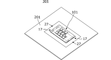
- FIG. 2 is a perspective view of the large circuit system 301 in a state where the circuit module 101 is mounted on the large circuit board 201.
- FIG. 3A is a cross-sectional view of a large circuit system 301 in a state where the circuit module 101 is mounted on the large circuit board 201.
- FIG. 3B is an enlarged view of a portion surrounded by a broken line in FIG. 3A.
- FIG. 4 is a perspective view of the circuit module 102 according to the second embodiment and the large circuit board 202 on which the circuit module 102 is mounted.
- FIG. 5A is a cross-sectional view of a large circuit system in which the circuit module 102 is mounted on the large circuit board 202.
- FIG. 5B is an enlarged view of a portion surrounded by a broken line in FIG. 5A.
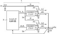
- FIG. 6 is a circuit diagram of a DC-DC converter according to a third embodiment.
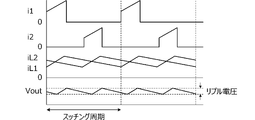
- FIG. 7 is a waveform diagram of voltage and current of each part of the switching power supply device shown in FIG.
- FIG. 8 is a circuit diagram of a DC-DC converter including four inductors L1, L2, L3, L4 and a power conversion circuit 1.
- FIG. 1 is a perspective view of the circuit module 101 according to the first embodiment and the large circuit board 201 on which the circuit module 101 is mounted.
- FIG. 2 is a perspective view of the large circuit system 301 in a state where the circuit module 101 is mounted on the large circuit board 201.
- the large circuit board 201 is, for example, a system board for a server, and various electronic components including a processor are mounted on it.
- 1 and 2 are perspective views of the large circuit board 201 as viewed from the back surface side, and various electronic components including the processor are mounted on the front surface of the large circuit board 201 (back surface in FIGS. 1 and 2). There is.
- the circuit module 101 includes a circuit module board 10 having a smaller area than the large circuit board 201.
- the circuit module 101 is, for example, a power supply circuit module, and is connected to the processor at the shortest distance.
- the circuit module 101 includes a circuit module board 10, an electronic circuit component 11 mounted on the circuit module board 10, and a circuit module board side fitting structure portion 17 provided on the circuit module board 10.
- the large circuit board 201 is provided with a large circuit board side fitting structure 27. Further, the large circuit board 201 is formed with a non-conductive thermal adhesive layer 15 on a surface facing the circuit module board 10.
- the circuit module board side fitting structure portion 17 and the large circuit board side fitting structure portion 27 are electrically connected and mechanically fixed. Further, the facing surfaces of the circuit module board 10 and the large circuit board 201 are electrically insulated by the non-conductive thermal adhesive layer 15 and thermally bonded.
- FIG. 3A is a cross-sectional view of a large circuit system 301 in a state where the circuit module 101 is mounted on the large circuit board 201.
- FIG. 3B is an enlarged view of a portion surrounded by a broken line in FIG. 3A.
- the large circuit board 201 has large circuit board side electronic components 21A and 21B mounted on the surface of the base material 20 (the lower surface in the orientation shown in FIGS. 3A and 3B).
- the electronic component 21A on the large circuit board side is, for example, a processor.
- connection pins 12 are inserted into these through vias 13 from the lower surface of the circuit module board 10 (the surface opposite to the mounting surface of the electronic circuit component 11). As shown in FIG. 3B, the connection pin 12 is formed with a protrusion 12P that abuts on the circuit module substrate 10.
- the through via 13 is a copper film formed on the inner wall surface of the cylindrical through hole formed in the circuit module substrate 10. One end of the connection pin 12 protrudes from the upper surface of the circuit module board 10, and the protruding portion is soldered with solder 14.
- the connection pin 12 is an example of the “circuit module board side connection terminal” according to the present invention.
- a plurality of pin sockets 22 are formed on the base material 20 of the large circuit board 201.
- the connection pin 12 of the circuit module 101 is inserted and fitted into the pin socket 22.
- the connection pin 12 is electrically connected to the pin socket 22 and is mechanically fixed.
- the connection pin 12 has a spring portion 12S and elastically contacts the pin socket 22.
- connection pin 12, the penetrating via 13, and the solder 14 on the circuit module 101 side constitute the fitting structure portion 17 on the circuit module board side. Further, the pin socket 22 on the large circuit board 201 side constitutes the fitting structure portion 27 on the large circuit board side.
- the base material 20 of the large circuit board 201 is formed with a non-conductive thermal adhesive layer 15 on the surface facing the circuit module board 10.
- the non-conductive heat-adhesive layer 15 is made of a non-conductive heat-conductive material, and is interposed on the facing surface between the circuit module board 10 and the base material 20 of the large circuit board 201, whereby the circuit module board 10 is formed.
- the base material 20 of the large circuit board 201 are thermally bonded in an electrically insulated state.
- a heat sink adhesive TIM: Thermal Interface Material
- the manufacturing procedure of the large circuit system 301 is as follows.
- connection pin 12 Inserts the connection pin 12 into the circuit module board 10 and solder it.
- the non-conductive thermal adhesive layer 15 is applied to the large circuit board 201.
- connection pin 12 of the circuit module 101 is inserted and fitted into the pin socket 22 of the large circuit board 201.
- the non-conductive thermal adhesive layer 15 is cured by leaving the large circuit board 201 and the circuit module 101 in a predetermined temperature atmosphere for a predetermined time.
- the non-conductive thermal adhesive layer 15 may be applied to the circuit module 101 side. Further, the pin socket 22 may be a penetrating via.
- the plurality of connection pins 12 include an electric signal terminal constituting an electric signal path and a large current terminal constituting a large current path of the electric power system.
- the current flowing in this large current path is 100 times or more the current flowing in the electric signal path.
- the circuit configured on the circuit module board 10 including the electronic circuit component 11 mounted on the circuit module board 10 constitutes a DC-DC converter.
- This DC-DC converter receives electric power from a circuit formed on the large circuit board 201, supplies the large current to the large circuit board 201, and outputs a DC voltage.
- a thin planar array winding inductor is formed on the circuit module board 10, or a molded inductor is mounted, and a switching element and a smoothing capacitor are mounted on the circuit module board 10.
- the circuit module board side fitting structure portion 17 and the large circuit board side fitting structure portion 27 are located on two opposite sides of the circuit module board 10, but one of the sides is the input portion of the DC-DC converter. The other side is the output section of the DC-DC converter.
- the electronic circuit component 11 is a switch element such as a MOS-FET.
- This DC-DC converter is mainly a power supply circuit for the electronic component 21A (processor) on the large circuit board side.
- This DC-DC converter acts as a POL (Point Of Load) converter that supplies a large current exceeding several tens of A and several hundreds of A to the processor, for example.
- the DC-DC converter inputs, for example, DC48V or DC12V from the large circuit board 201, steps down to DC6V to 1V or DC1.8V to 0.5V, and supplies the DC-DC converter to the processor.
- the MOS-FET and inductor of the circuit module 101 generate heat due to power loss, but since the circuit module 101 is thermally bonded to the large circuit board 201 through the non-conductive thermal adhesive layer 15, the circuit module 101 and the large circuit board 201 The combined heat capacity is large, and the heat dissipated from the heat generated by the circuit module 101 is high.
- connection pin 12 on the circuit module 101 side is inserted into the pin socket 22 of the large circuit board 201.
- a frame is provided on the circuit module 101 side and a frame is provided on the large circuit board 201 side.
- the frame socket may be provided in which the frame is inserted, or the frame may be inserted into the large circuit board 201 side to mechanically fix the frame to the large circuit board 201 side.
- the circuit module since the circuit module is not molded, it can be configured to be thin as a whole and the cost can be reduced. Moreover, even though it is not molded, the facing surfaces of the circuit module board 10 and the large circuit board 201 are surface-bonded through the non-conductive heat-bonding layer 15, so that the heat distribution is equalized in the surface direction. Therefore, the heat dissipation effect of the circuit module 101 is high.
- the non-conductive heat-adhesive layer 15 is a cured layer of a liquid TIM material, the adhesion of the circuit module 101 to the large circuit board 201 is high. Therefore, it is not necessary to screw the circuit module 101 to the large circuit board 201, for example. Further, higher thermal conductivity can be obtained as compared with a structure in which a thermally conductive silicon sheet is screwed between the large circuit board 201 and the circuit module 101.
- the thermal conductivity of the silicon sheet is 1 W / mK
- the thermal conductivity of the non-conductive thermal adhesive layer 15 is 2 W / mK.
- a large-scale circuit system mounted on the above can be obtained, and the conduction of a large current 100 times or more that of the current flowing through the connection terminals on the board side of multiple circuit modules, the connection of electrical signals, the mechanical fixation, and the uniformization of heat distribution can be achieved at the same time. realizable.
- the electric connection portion of the circuit module to the large circuit board is a power system that supplies a large current 100 times or more as large as that of the electric signal system that transmits a control signal and the like and the current that flows through the electric signal system.
- FIG. 4 is a perspective view of the circuit module 102 according to the second embodiment and the large circuit board 202 on which the circuit module 102 is mounted. Similar to the example shown in the first embodiment, FIG. 4 is a perspective view of the back surface side of the large circuit board 202, and various electronic components including the processor are the front surface of the large circuit board 202 (in FIG. 4). It is mounted on the back side).
- the circuit module 102 includes a circuit module board 10, an electronic circuit component 11 mounted on the circuit module board 10, a circuit module board side fitting structure portion 17 provided on the circuit module board 10, and a circuit module board side connection portion 18. Be prepared.
- the large circuit board 202 is provided with a large circuit board side fitting structure portion 27 and a large circuit board side connection portion 28. Further, the large circuit board 202 is formed with a non-conductive thermal adhesive layer 15 on a surface facing the circuit module board 10.
- circuit module board side fitting structure portion 17 and the large circuit board side fitting structure portion 27 are electrically connected and mechanically fixed. Further, the circuit module board side connection portion 18 and the large circuit board side connection portion 28 are electrically connected. Further, the facing surfaces of the circuit module board 10 and the large circuit board 202 are electrically insulated by the non-conductive thermal adhesive layer 15 and thermally bonded.
- FIG. 5A is a cross-sectional view of a large circuit system in which the circuit module 102 is mounted on the large circuit board 202. This cross-sectional position is a surface passing through the circuit module board side connection portion 18 and the large circuit board side connection portion 28 shown in FIG. 3 (A).
- FIG. 5B is an enlarged view of a portion surrounded by a broken line in FIG. 5A.
- the large circuit board 202 has large circuit board side electronic components 21A and 21B mounted on the surface of the base material 20 (the lower surface in the orientation shown in FIGS. 4A and 4B).
- the electronic component 21A on the large circuit board side is, for example, a processor.
- a plurality of conductive joints 16 are formed by applying a conductive paste to the large circuit board side connection portion 28 of the large circuit board 202.
- the circuit module board side connection portion 18 of the circuit module 102 is electrically connected to the large circuit board side connection portion 28 of the large circuit board 202 through the conductive joint portion 16.
- the non-conductive thermal adhesive layer 15 and the conductive joint portion 16 are solidified bodies of a paste containing a main material of the same system, and the conductive joint portion 16 is a solidified body of a conductive paste containing a conductive filler in the main material.
- the conductive filler is, for example, silver powder or copper powder.
- the non-conductive heat-bonding filler is, for example, a powder of alumina or aluminum nitride.
- the main material is, for example, an epoxy resin.
- the circuit module substrate 10 is a glass epoxy substrate, an aluminum nitride substrate or an alumina substrate suitable for the above conductive paste.
- the current flowing through the circuit module board side fitting structure portion 17 is 100 times or more the current flowing through the plurality of circuit module board side connection portions 18.
- the manufacturing procedure of the large circuit system 302 is as follows.
- connection pin 12 Inserts the connection pin 12 into the circuit module board 10 and solder it.
- a conductive paste for forming the conductive joint portion 16 is applied to the circuit module substrate 10.
- the non-conductive thermal adhesive layer 15 is applied to the large circuit board 201.
- connection pin 12 of the circuit module 101 is inserted and fitted into the pin socket 22 of the large circuit board 201.
- the non-conductive thermal adhesive layer 15 is cured by leaving the large circuit board 201 and the circuit module 101 in a predetermined temperature atmosphere for a predetermined time. Further, the conductive paste is solidified to form the conductive joint portion 16.
- the circuit module board side fitting structure portion 17 and the large circuit board side fitting structure portion 27 are power system fitting structure parts that supply a large current 100 times or more as large as the current flowing through the electric signal system. Is. Further, the circuit module board side connection portion 18 and the large circuit board side connection portion 28 are connection portions of the electric signal system.
- the conductive joint portion 16 is a solidified portion of the conductive paste having higher thermal conductivity than the non-conductive thermal adhesive layer 15.
- the electronic signal is, for example, a control signal for a DC-DC converter or a signal indicating the state of the DC-DC converter.
- the present embodiment it is possible to reduce the power loss due to the resistance component in the path at the connection part of the power system that supplies a large current 100 times or more as large as the current flowing through the electric signal system, and at the connection part of the electronic signal system.
- the arrangement pitch can be made finer, and the density can be increased in the plane direction.
- FIG. 6 is a circuit diagram of the DC-DC converter according to the third embodiment.
- This DC-DC converter steps down the input voltage Vin from the input unit Pi and outputs the output voltage Vout from the output unit Po.
- the DC-DC converter includes a planar array winding constituting the inductors L1 and L2, and a power conversion circuit 1.
- the switching circuit units 2a and 2b of the power conversion circuit 1 are composed of a high-side MOS-FET and a low-side MOS-FET, respectively.
- the first end of the inductor L1 is connected to the output unit of the switching circuit unit 2a, and the second end is connected to the common output unit Po.
- the first end of the inductor L2 is connected to the output unit of the switching circuit unit 2b, and the second end is connected to the common output unit Po.
- a smoothing capacitor Co is connected to the output unit Po.
- a drive circuit 3a is connected between the gate and source of the MOS-FET of the switching circuit unit 2a, and a drive circuit 3b is connected between the gate and source of the MOS-FET of the switching circuit unit 2b.
- the switching control circuit 4 is connected to the drive circuits 3a and 3b.
- the switching control circuit 4 outputs a two-phase drive signal having a phase difference of 180 degrees to the drive circuits 3a and 3b.
- FIG. 7 is a waveform diagram of voltage and current of each part of the switching power supply device shown in FIG.
- the voltage Vin is an input voltage.
- the current i1 is an input current flowing through the switching circuit unit 2a
- the current i2 is an input current flowing through the switching circuit unit 2b.
- the current iL1 is a current flowing through the inductor L1
- the current iL2 is a current flowing through the inductor L2.
- the voltage Vout is the output voltage of the output unit Po.
- the phase difference of the current waveforms of the input currents i1 and i2 is 180 degrees, and the phase difference of the waveforms of the currents flowing through the inductors L1 and L2 is also 180 degrees.
- the two-phase switching power supply device uses two inductors, two sets of switching operations are performed in one switching cycle, and the waveform of the exciting current in the two inductor currents. Can be confirmed.
- FIG. 8 is a circuit diagram of a DC-DC converter including four inductors L1, L2, L3, L4 each consisting of windings and a power conversion circuit 1.
- the switching circuit units 2a, 2b, 2c, and 2d of the power conversion circuit 1 are composed of a high-side MOS-FET and a low-side MOS-FET, respectively.
- the first ends of the inductors L1, L2, L3, and L4 are connected to the output units of the switching circuit units 2a, 2b, 2c, and 2d, respectively, and the second end is connected to the common output unit Po.
- Drive circuits (not shown) are connected to the switching circuit units 2a, 2b, 2c, and 2d, respectively, and the switching control circuit 4 is connected to each drive circuit.
- the switching control circuit 4 outputs a four-phase drive signal having a phase difference of 90 degrees to the drive circuit.
- the phase difference of the input current waveforms flowing through the switching circuit units 2a, 2b, 2c, and 2d is 90 degrees, and the waveforms of the currents flowing through the inductors L1, L2, L3, and L4.
- the phase difference of is also 90 degrees. Therefore, four sets of switching operations are performed in one switching cycle, and the waveform of the exciting current at the four inductor currents can be confirmed.
- the switching control circuit 4 shown in FIG. 8 is a multi-phase PWM controller, and can control the number of switching circuit units to be used among the plurality of switching circuit units 2a to 2d according to the lightness and weight of the load. That is, it operates in a single phase at the lightest load, operates in four phases at the heaviest load, and operates in two or three phases at a moderate load.
- FIG. 8 The example shown in FIG. 8 is a multi-phase DC-DC converter up to 4 phases, but a multi-phase multi-phase DC-DC converter may be further configured in the same manner.
Landscapes
- Engineering & Computer Science (AREA)
- Microelectronics & Electronic Packaging (AREA)
- Power Engineering (AREA)
- Manufacturing & Machinery (AREA)
- Combinations Of Printed Boards (AREA)
- Structures For Mounting Electric Components On Printed Circuit Boards (AREA)
- Dc-Dc Converters (AREA)
Abstract
回路モジュール(101)は、大型回路基板(201)より小面積の回路モジュール基板(10)と、回路モジュール基板(10)に実装された電子回路部品(11)と、回路モジュール基板(10)に設けられた接続ピン(12)と、回路モジュール基板(10)に設けられた回路モジュール基板側嵌合構造部(17)と、を備える。ピンソケット(22)と接続ピン(12)とは電気的に接続され、回路モジュール基板(10)と大型回路基板(201)の基材(20)との対向面間には、非導電性の熱伝導性材により電気的に絶縁され熱的に接合する非導電性熱接着層(15)が形成されている。
Description
本発明は、大型回路基板に取り付けられる回路モジュール基板に関し、特に、はんだを用いないで大型回路基板に取り付けられる回路モジュール基板及びそれを備える大型回路システムに関する。
特許文献1には、回路基板と、その回路基板上に実装される電子部品とによって構成される電子モジュールに関し、回路基板の下面に放熱板が対向配置され、巻線部品の下面と回路基板の上面との間に熱伝導体が充填された電子モジュールが示されている。
モジュール基板を備える回路モジュールを、例えば、大型の回路基板の裏面に実装する場合、一般的には、大型基板にモジュール基板を接着剤等で仮止めすることでモジュール基板の落下を防止した上で、リフロー炉を通すことによってはんだ付けを行う。
一方、低背化や組み立てコストの低減などのために、モールドしない状態の回路モジュールを大型回路基板の裏面に実装する場合、回路モジュールを構成する各種部品は既にはんだ付けによって実装されているため、回路モジュールを大型の回路基板に実装すると、回路モジュールを構成する部品を取り付けていたはんだが再溶融して、部品の位置がずれたり、自重により落下したりする、などの問題が生じる。
したがって、モールドしていない回路モジュールを大型回路基板へ実装する技術が必要となる。
回路モジュールを構成する各種部品を高融点はんだを用いて実装することで、大型回路基板のリフロー時にはんだの再溶融を避ける方法が考えられるが、部品の耐熱性の制限やはんだの選択肢が限られるので、現実的には難しい。
また、既に回路部品が実装された大型回路基板に、後から回路モジュールを低融点はんだで実装する方法も考えられる。しかし、低融点はんだの場合、実動作中に回路の発熱によって瞬時においてもはんだが溶融するような事態になれば、部品の接続不良が発生する場合があり、信頼性の面で大きな問題となる。例えば、回路モジュールの近くにプロセッサなどの発熱部品が実装されていたり、回路モジュールが自己発熱の大きな部品を備えていたりする場合に、問題が顕在化しやすい。
一方、はんだに代わる接続方法として、銀ペーストのような金属フィラーを含む導電ペーストによる接続方法がある。導電性を上げるには金属フィラーを多量に含むものを使用すればよいが、接着強度が弱くなるので限界がある。つまり、導電性と接着強度はトレードオフの関係にある。
そこで、本発明の目的は、はんだ付けを用いなくても、大型回路基板に回路モジュールを実装した大型回路システムにおいて高い信頼性および優れた電気特性を実現することにある。
本開示の一例としての回路モジュールは、大型回路基板側嵌合構造部を有する大型回路基板に実装され、前記大型回路基板より小面積の回路モジュール基板と、前記回路モジュール基板に実装された電子回路部品と、前記回路モジュール基板に設けられた複数の回路モジュール基板側接続端子と、前記回路モジュール基板に設けられた回路モジュール基板側嵌合構造部と、を備える。そして、前記複数の回路モジュール基板側接続端子は、電気信号経路を構成する電気信号端子と、電力系の大電流経路を構成する大電流端子とを備え、前記大型回路基板に設けられた複数の大型回路基板側接続端子と前記複数の回路モジュール基板側接続端子とは電気的に接続され、前記回路モジュール基板側嵌合構造部と前記大型回路基板側嵌合構造部とは電気的に接続され且つ機械的に固定され、前記回路モジュール基板と前記大型回路基板の基材との対向面間に、非導電性の熱伝導性材により電気的に絶縁され熱的に接合する非導電性熱接着層が形成された、ことを特徴とする。
本開示の大型回路システムは、上記回路モジュールと、当該回路モジュールが実装された大型回路基板とで構成される。
本発明によれば、はんだ付けを用いなくても、大型回路基板に回路モジュールを実装する構造に対して、高い信頼性および優れた電気特性を実現できる。
以降、図を参照して幾つかの具体的な例を挙げて、本発明を実施するための複数の形態を示す。各図中には同一箇所に同一符号を付している。要点の説明又は理解の容易性を考慮して、実施形態を説明の便宜上、複数の実施形態に分けて示すが、異なる実施形態で示した構成の部分的な置換又は組み合わせは可能である。第2の実施形態以降では第1の実施形態と共通の事柄についての記述を省略し、異なる点についてのみ説明する。特に、同様の構成による同様の作用効果については実施形態毎には逐次言及しない。
《第1の実施形態》
図1は、第1の実施形態に係る回路モジュール101と、この回路モジュール101が実装される大型回路基板201の斜視図である。図2は大型回路基板201に回路モジュール101が実装された状態の大型回路システム301の斜視図である。
図1は、第1の実施形態に係る回路モジュール101と、この回路モジュール101が実装される大型回路基板201の斜視図である。図2は大型回路基板201に回路モジュール101が実装された状態の大型回路システム301の斜視図である。
大型回路基板201は例えばサーバ用のシステムボードであり、プロセッサを含む各種電子部品が実装されている。図1、図2においては、大型回路基板201の裏面側を視た斜視図であり、上記プロセッサを含む各種電子部品は大型回路基板201の表面(図1、図2における裏面)に実装されている。
図1に示すように、回路モジュール101は、大型回路基板201より小面積の回路モジュール基板10を備える。回路モジュール101は例えば電源回路モジュールであり、上記プロセッサに最短距離で接続される。
回路モジュール101は、回路モジュール基板10と、それに実装された電子回路部品11と、回路モジュール基板10に設けられた回路モジュール基板側嵌合構造部17と、を備える。
大型回路基板201には大型回路基板側嵌合構造部27が設けられている。また、大型回路基板201には、回路モジュール基板10との対向面に非導電性熱接着層15が形成されている。
図2に表れているように、回路モジュール基板側嵌合構造部17と大型回路基板側嵌合構造部27とは電気的に接続され且つ機械的に固定される。また、回路モジュール基板10と大型回路基板201との対向面間は非導電性熱接着層15によって電気的に絶縁され熱的に接合される。
図3(A)は、大型回路基板201に回路モジュール101が実装された状態の大型回路システム301の断面図である。図3(B)は図3(A)における破線で囲んだ部分の拡大図である。
大型回路基板201は、その基材20の表面(図3(A)、図3(B)に示す向きでは下面)に大型回路基板側電子部品21A,21Bが実装されている。大型回路基板側電子部品21Aは例えばプロセッサである。
回路モジュール101の回路モジュール基板10には複数の貫通ビア13が形成されている。これら貫通ビア13には、回路モジュール基板10の下面(電子回路部品11の実装面とは反対側の面)から接続ピン12がそれぞれ挿入されている。図3(B)に表れているように、接続ピン12には、回路モジュール基板10に当接する突起部12Pが形成されている。貫通ビア13は回路モジュール基板10に形成された円筒形の貫通孔の内壁面に形成された銅膜である。接続ピン12の一方端は回路モジュール基板10の上面から突出し、その突出部がはんだ14ではんだ付けされている。接続ピン12は本発明に係る「回路モジュール基板側接続端子」の一例である。
大型回路基板201の基材20には複数のピンソケット22が形成されている。回路モジュール101の接続ピン12はピンソケット22に挿入嵌合される。そのことにより、接続ピン12はピンソケット22に対して電気的に接続され、且つ機械的に固定される。接続ピン12はバネ部12Sを有し、ピンソケット22に対して弾性的に接触する。
回路モジュール101側の接続ピン12、貫通ビア13及びはんだ14は上記回路モジュール基板側嵌合構造部17を構成する。また、大型回路基板201側のピンソケット22は上記大型回路基板側嵌合構造部27を構成する。
大型回路基板201の基材20には、回路モジュール基板10との対向面に非導電性熱接着層15が形成されている。この非導電性熱接着層15は非導電性の熱伝導性材で構成されていて、回路モジュール基板10と大型回路基板201の基材20との対向面に介在することにより、回路モジュール基板10と大型回路基板201の基材20とを電気的に絶縁状態で熱的に接合する。非導電性熱接着層15にはヒートシンク用接着材(TIM:Thermal Interface Material)を用いることができる。
大型回路システム301の製造手順は次のとおりである。
(1)回路モジュール基板10に接続ピン12を挿入し、はんだ付けする。
(2)大型回路基板201に非導電性熱接着層15を塗布する。
(3)回路モジュール101の接続ピン12を大型回路基板201のピンソケット22に挿入嵌合させる。
(4)大型回路基板201及び回路モジュール101を所定温度雰囲気中に所定時間放置することによって非導電性熱接着層15を硬化させる。
なお、非導電性熱接着層15は回路モジュール101側に塗布してもよい。また、ピンソケット22は貫通ビアであってもよい。
複数の接続ピン12は、電気信号経路を構成する電気信号端子と、電力系の大電流経路を構成する大電流端子とを備える。この大電流経路に流れる電流は電気信号経路に流れる電流の100倍以上である。
回路モジュール基板10に実装された電子回路部品11を含んで、回路モジュール基板10に構成される回路はDC-DCコンバータを構成する。このDC-DCコンバータは、大型回路基板201に形成されている回路から電力を受けて、大型回路基板201に対して、上記大電流を供給して直流電圧を出力する。回路モジュール基板10には薄型の平面アレイ巻線のインダクタが形成されているか、モールドされたインダクタが実装され、スイッチング素子や平滑コンデンサは回路モジュール基板10に実装されている。
図2において、回路モジュール基板側嵌合構造部17及び大型回路基板側嵌合構造部27は回路モジュール基板10の対向する2辺にあるが、その一方の辺はDC-DCコンバータの入力部であり、他方の辺はDC-DCコンバータの出力部である。電子回路部品11は例えばMOS-FET等のスイッチ素子である。このDC-DCコンバータは主に大型回路基板側電子部品21A(プロセッサ)の電源回路である。このDC-DCコンバータはプロセッサに、例えば、数10A、また数100Aを超える大電流を供給するPOL(Point Of Load)コンバータとして作用する。DC-DCコンバータは大型回路基板201の基材20を挟んでプロセッサの最短距離に配置されるため、数10A、また数100Aを超える大電流線路での抵抗成分による電力損失が最小限なものとなる。
DC-DCコンバータは、大型回路基板201から例えばDC48V又はDC12Vを入力し、DC6V~1V又はDC1.8V~0.5Vに降圧し、プロセッサに与える。
回路モジュール101のMOS-FETやインダクタは電力損失によって発熱するが、回路モジュール101は非導電性熱接着層15を通して大型回路基板201と熱的に接合されるので、回路モジュール101と大型回路基板201を合わせた熱容量が大きく、回路モジュール101で発生される熱の放熱性は高い。
以上に示した例では、回路モジュール101側の接続ピン12が大型回路基板201のピンソケット22に挿入される例を示したが、回路モジュール101側にフレームを設け、大型回路基板201側にフレームが挿入されるフレームソケットを設けたり、大型回路基板201側にフレームを挿入して機械的にフレームを大型回路基板201側に固定したりしてもよい。
本実施形態によれば、回路モジュールはモールドしていないので、全体に薄型に構成でき、低コスト化できる。しかも、モールドしていないにもかかわらず、回路モジュール基板10と大型回路基板201との対向面間が非導電性熱接着層15を通して面接合しているので、熱分布は面方向に均等化されて、回路モジュール101の放熱効果が高い。
また、非導電性熱接着層15は液状のTIM材の硬化層であるので、大型回路基板201に対する回路モジュール101の密着性が高い。そのため、大型回路基板201に対して回路モジュール101を例えばねじ留めする必要がない。さらに、大型回路基板201と回路モジュール101との間に熱伝導性のシリコンシートを通してねじ留めした構造に比べて高い熱伝導性が得られる。シリコンシートの熱伝導性は1W/mKであるのに対し、非導電性熱接着層15の熱伝導性は、2W/mKである。
また、大型回路基板201と回路モジュール101とを非導電性熱接着層15を通して接合させたことにより、ピンソケット22に対する接続ピン12の押さえ込み力が強化される。
このように、本実施形態の構成を用いることで、はんだ付け以外の方法でも大型回路基板に実装可能であって、モールドされていない回路基板構造の回路モジュール、及びその回路モジュールが大型回路の基板に実装された大型回路システムが得られ、複数の回路モジュール基板側接続端子に流す電流に比べて100倍以上の大電流の導通と電気信号の接続、機械的固定、熱分布の均一化を同時に実現できる。
《第2の実施形態》
第2の実施形態では、大型回路基板に対する回路モジュールの電気的接続部について、制御信号などを伝送する電気信号系と電気信号系に流す電流に比べて100倍以上の大電流を供給する電力系とで構造が異なる回路モジュール及び大型回路システムを例示する。
第2の実施形態では、大型回路基板に対する回路モジュールの電気的接続部について、制御信号などを伝送する電気信号系と電気信号系に流す電流に比べて100倍以上の大電流を供給する電力系とで構造が異なる回路モジュール及び大型回路システムを例示する。
図4は、第2の実施形態に係る回路モジュール102と、この回路モジュール102が実装される大型回路基板202の斜視図である。第1の実施形態で示した例と同様に、図4においては、大型回路基板202の裏面側を視た斜視図であり、プロセッサを含む各種電子部品は大型回路基板202の表面(図4における裏面)に実装されている。
回路モジュール102は、回路モジュール基板10と、それに実装された電子回路部品11と、回路モジュール基板10に設けられた回路モジュール基板側嵌合構造部17と、回路モジュール基板側接続部18と、を備える。
大型回路基板202には大型回路基板側嵌合構造部27及び大型回路基板側接続部28が設けられている。また、大型回路基板202には、回路モジュール基板10との対向面に非導電性熱接着層15が形成されている。
回路モジュール基板側嵌合構造部17と大型回路基板側嵌合構造部27とは電気的に接続され且つ機械的に固定される。また、回路モジュール基板側接続部18と大型回路基板側接続部28とは電気的に接続される。さらに、回路モジュール基板10と大型回路基板202との対向面間は非導電性熱接着層15によって電気的に絶縁され熱的に接合される。
図5(A)は、大型回路基板202に回路モジュール102が実装された状態の大型回路システムの断面図である。この断面位置は、図3(A)に示した回路モジュール基板側接続部18及び大型回路基板側接続部28を通る面である。図5(B)は図5(A)における破線で囲んだ部分の拡大図である。
大型回路基板202は、その基材20の表面(図4(A)、図4(B)に示す向きでは下面)に大型回路基板側電子部品21A,21Bが実装されている。大型回路基板側電子部品21Aは例えばプロセッサである。
大型回路基板202の大型回路基板側接続部28には導電性ペーストの塗布による複数の導電性接合部16が形成されている。回路モジュール102の回路モジュール基板側接続部18は導電性接合部16を通して大型回路基板202の大型回路基板側接続部28に電気的に接続される。
非導電性熱接着層15と導電性接合部16とは、同系統の主材を含むペーストの固化体であり、導電性接合部16は主材に導電性フィラーを含む導電性ペーストの固化体である。導電性フィラーは例えば銀粉や銅粉である。非導電性熱接着フィラーは例えばアルミナや窒化アルミの粉である。また、主材は例えばエポキシ樹脂である。
回路モジュール基板10はガラスエポキシ基板や上記導電性ペーストに適した窒化アルミニウム基板やアルミナ基板である。
回路モジュール基板側嵌合構造部17に流れる電流は、複数の回路モジュール基板側接続部18に流れる電流に比べて100倍以上である。
大型回路システム302の製造手順は次のとおりである。
(1)回路モジュール基板10に接続ピン12を挿入し、はんだ付けする。
(2)回路モジュール基板10に、導電性接合部16形成用の導電性ペーストを塗布する。
(3)大型回路基板201に非導電性熱接着層15を塗布する。
(4)回路モジュール101の接続ピン12を大型回路基板201のピンソケット22に挿入嵌合させる。
(5)大型回路基板201及び回路モジュール101を所定温度雰囲気中に所定時間放置することによって非導電性熱接着層15を硬化させる。また、導電性ペーストを固化させて導電性接合部16を形成する。
本実施形態において、回路モジュール基板側嵌合構造部17及び大型回路基板側嵌合構造部27は電気信号系に流す電流に比べて100倍以上の大電流を供給する電力系の嵌合構造部である。また、回路モジュール基板側接続部18及び大型回路基板側接続部28は電気信号系の接続部である。そして、導電性接合部16は、非導電性熱接着層15よりも熱伝導性の高い、導電性ペーストの固化部である。上記電子信号としては、例えばDC-DCコンバータに対する制御信号やDC-DCコンバータの状態を示す信号である。
本実施形態によれば、電気信号系に流す電流に比べて100倍以上の大電流を供給する電力系の接続部ではその経路における抵抗成分による電力損失を低減でき、電子信号系の接続部では、その配置ピッチを細かくすることができ、面方向での高密度化を図れる。
《第3の実施形態》
第3の実施形態では、回路モジュールに構成される回路について例示する。
第3の実施形態では、回路モジュールに構成される回路について例示する。
図6は第3の実施形態に係るDC-DCコンバータの回路図である。このDC-DCコンバータは入力部Piからの入力電圧Vinを降圧して出力部Poから出力電圧Voutを出力する。DC-DCコンバータはインダクタL1,L2を構成する平面アレイ巻線と、電力変換回路1と、を備える。電力変換回路1のスイッチング回路部2a,2bは、それぞれハイサイドのMOS-FETとローサイドのMOS-FETとで構成されている。インダクタL1の第1端はスイッチング回路部2aの出力部に接続されていて、第2端は共通の出力部Poに接続されている。インダクタL2の第1端はスイッチング回路部2bの出力部に接続されていて、第2端は共通の出力部Poに接続されている。出力部Poには平滑コンデンサCoが接続されている。
前記スイッチング回路部2aのMOS-FETのゲート・ソース間には駆動回路3aが接続されていて、前記スイッチング回路部2bのMOS-FETのゲート・ソース間には駆動回路3bが接続されている。
駆動回路3a,3bにはスイッチング制御回路4が接続されている。このスイッチング制御回路4は駆動回路3a,3bに対して、位相差180度の2相の駆動信号を出力する。
図7は、図6に示したスイッチング電源装置の各部の電圧・電流の波形図である。図7において、電圧Vinは入力電圧である。電流i1はスイッチング回路部2aに流れる入力電流であり、電流i2はスイッチング回路部2bに流れる入力電流である。また、電流iL1はインダクタL1に流れる電流であり、電流iL2はインダクタL2に流れる電流である。電圧Voutは、出力部Poの出力電圧である。
入力電流i1,i2の電流波形の位相差は180度であり、インダクタL1,L2に流れる電流の波形の位相差も180度である。図6、図7に示した例では、二つのインダクタを用いた2相のスイッチング電源装置であるので、1スイッチング周期に2組のスイッチング動作が行われ、2回のインダクタ電流における励磁電流の波形が確認できる。
図8は、それぞれ巻線からなる四つのインダクタL1,L2,L3,L4と、電力変換回路1と、を備えるDC-DCコンバータの回路図である。電力変換回路1のスイッチング回路部2a,2b,2c,2dは、それぞれハイサイドのMOS-FETとローサイドのMOS-FETとで構成されている。インダクタL1,L2,L3,L4のそれぞれの第1端はスイッチング回路部2a,2b,2c,2dの出力部にそれぞれ接続されていて、第2端は共通の出力部Poに接続されている。
スイッチング回路部2a,2b,2c,2dには図外の駆動回路がそれぞれ接続されていて、各駆動回路にスイッチング制御回路4が接続されている。このスイッチング制御回路4は駆動回路に対して、位相差90度の四相の駆動信号を出力する。
このように4相のスイッチング電源装置であれば、スイッチング回路部2a,2b,2c,2dに流れる入力電流波形の位相差は90度であり、インダクタL1,L2,L3,L4に流れる電流の波形の位相差も90度である。したがって、1スイッチング周期に4組のスイッチング動作が行われ、4回のインダクタ電流における励磁電流の波形が確認できる。
図8に示したスイッチング制御回路4は、マルチフェーズのPWMコントローラであり、負荷の軽重に応じて、複数のスイッチング回路部2a~2dのうち、用いるスイッチング回路部の数を制御することもできる。つまり、最軽負荷時には単相で動作し、最重負荷時には4相で動作し、その中程度の負荷時には2相又は3相で動作する。
図8に示した例は4相までのマルチフェーズDC-DCコンバータであるが、同様にして更に多相のマルチフェーズDC-DCコンバータを構成してもよい。
最後に、本発明は上述した実施形態に限られるものではない。当業者によって適宜変形及び変更が可能である。本発明の範囲は、上述の実施形態ではなく、特許請求の範囲によって示される。さらに、本発明の範囲には、特許請求の範囲内と均等の範囲内での実施形態からの変形及び変更が含まれる。
Co…平滑コンデンサ
L1,L2,L3,L4…インダクタ
Pi…入力部
Po…出力部
1…電力変換回路
2a,2b,2c,2d…スイッチング回路部
3a,3b…駆動回路
4…スイッチング制御回路
10…回路モジュール基板
11…電子回路部品
12…接続ピン(回路モジュール基板側接続端子)
12P…突起部
12S…バネ部
13…貫通ビア
14…はんだ
15…非導電性熱接着層
16…導電性接合部
17…回路モジュール基板側嵌合構造部
18…回路モジュール基板側接続部
20…大型回路基板の基材
21A,21B…大型回路基板側電子部品
22…ピンソケット(大型回路基板側接続端子)
27…大型回路基板側嵌合構造部
28…大型回路基板側接続部
101,102…回路モジュール
201,202…大型回路基板
301,302…大型回路システム
L1,L2,L3,L4…インダクタ
Pi…入力部
Po…出力部
1…電力変換回路
2a,2b,2c,2d…スイッチング回路部
3a,3b…駆動回路
4…スイッチング制御回路
10…回路モジュール基板
11…電子回路部品
12…接続ピン(回路モジュール基板側接続端子)
12P…突起部
12S…バネ部
13…貫通ビア
14…はんだ
15…非導電性熱接着層
16…導電性接合部
17…回路モジュール基板側嵌合構造部
18…回路モジュール基板側接続部
20…大型回路基板の基材
21A,21B…大型回路基板側電子部品
22…ピンソケット(大型回路基板側接続端子)
27…大型回路基板側嵌合構造部
28…大型回路基板側接続部
101,102…回路モジュール
201,202…大型回路基板
301,302…大型回路システム
Claims (11)
- 大型回路基板側嵌合構造部を有する大型回路基板に実装され、前記大型回路基板より小面積の回路モジュール基板と、
前記回路モジュール基板に実装された電子回路部品と、
前記回路モジュール基板に設けられた複数の回路モジュール基板側接続端子と、
前記回路モジュール基板に設けられた回路モジュール基板側嵌合構造部と、
を備え、
前記複数の回路モジュール基板側接続端子は、電気信号経路を構成する電気信号端子と、電力系の大電流経路を構成する大電流端子とを備え、
前記大型回路基板に設けられた複数の大型回路基板側接続端子と前記複数の回路モジュール基板側接続端子とは電気的に接続され、
前記回路モジュール基板側嵌合構造部と前記大型回路基板側嵌合構造部とは電気的に接続され且つ機械的に固定され、
前記回路モジュール基板と前記大型回路基板の基材との対向面間に、非導電性の熱伝導性材により電気的に絶縁され熱的に接合する非導電性熱接着層が形成された、
回路モジュール。 - 前記回路モジュール基板側嵌合構造部は前記大型回路基板側嵌合構造部に嵌合するピン又はフレームである、
請求項1に記載の回路モジュール。 - 前記回路モジュール基板側嵌合構造部は前記電気信号経路及び前記電力系の大電流経路を構成し、当該大電流経路に流れる電流は前記電気信号経路に流れる電流の100倍以上である、
請求項1又は2に記載の回路モジュール。 - 前記回路モジュール基板に形成され、前記大型回路基板の基材に形成された複数の大型回路基板側接続部にそれぞれ対向する複数の回路モジュール基板側接続部と、
前記複数の回路モジュール基板側接続部を前記複数の大型回路基板側接続部に対して電気的に接続する導電性接合部と、を備える、
請求項1又は2に記載の回路モジュール。 - 前記回路モジュール基板側嵌合構造部に流れる電流は、前記複数の回路モジュール基板側接続部に流れる電流に比べて100倍以上である、
請求項4に記載の回路モジュール。 - 前記導電性接合部は銀粉をフィラーとして含む導電性ペーストの固化体である、
請求項4又は5に記載の回路モジュール。 - 前記非導電性熱接着層と前記導電性接合部とは、同系統の主材を含むペーストの固化体であり、前記導電性接合部は前記主材に導電性フィラーを含む導電性ペーストの固化体である、
請求項4から6のいずれかに記載の回路モジュール。 - 前記回路モジュール基板に実装された前記電子回路部品を含んで構成される回路は、前記大型回路基板に形成されている回路から電力を受けて、前記大型回路基板に形成されている回路へ前記大電流経路を通して大電流を供給するDC-DCコンバータを構成する、
請求項3に記載の回路モジュール。 - 前記回路モジュール基板に実装された前記電子回路部品を含んで構成される回路は、前記大型回路基板に形成されている回路から電力を受けて、前記大型回路基板に形成されている回路へ前記回路モジュール基板側嵌合構造部を通して大電流を供給するDC-DCコンバータを構成する、
請求項5に記載の回路モジュール。 - 前記DC-DCコンバータは、共通の出力部に電流を供給する電流経路に対して直列に接続される複数のインダクタと、当該複数のインダクタに流れるスイッチング電流をそれぞれ生成する複数のスイッチング素子と、当該複数のスイッチング素子を制御するスイッチング制御回路を備え、前記スイッチング制御回路は、前記複数のスイッチング素子にマルチフェーズ発振信号を与える、
請求項8又は9に記載の回路モジュール。 - 請求項1から10のいずれかに記載の回路モジュールと、当該回路モジュールが実装された前記大型回路基板と、で構成された大型回路システム。
Priority Applications (2)
| Application Number | Priority Date | Filing Date | Title |
|---|---|---|---|
| JP2022561845A JP7476980B2 (ja) | 2020-11-16 | 2021-11-03 | 回路モジュール及び大型回路システム |
| US18/313,180 US12369252B2 (en) | 2020-11-16 | 2023-05-05 | Circuit module and large-scale circuit system |
Applications Claiming Priority (2)
| Application Number | Priority Date | Filing Date | Title |
|---|---|---|---|
| JP2020-190082 | 2020-11-16 | ||
| JP2020190082 | 2020-11-16 |
Related Child Applications (1)
| Application Number | Title | Priority Date | Filing Date |
|---|---|---|---|
| US18/313,180 Continuation US12369252B2 (en) | 2020-11-16 | 2023-05-05 | Circuit module and large-scale circuit system |
Publications (1)
| Publication Number | Publication Date |
|---|---|
| WO2022102480A1 true WO2022102480A1 (ja) | 2022-05-19 |
Family
ID=81601220
Family Applications (1)
| Application Number | Title | Priority Date | Filing Date |
|---|---|---|---|
| PCT/JP2021/040473 Ceased WO2022102480A1 (ja) | 2020-11-16 | 2021-11-03 | 回路モジュール及び大型回路システム |
Country Status (3)
| Country | Link |
|---|---|
| US (1) | US12369252B2 (ja) |
| JP (1) | JP7476980B2 (ja) |
| WO (1) | WO2022102480A1 (ja) |
Citations (4)
| Publication number | Priority date | Publication date | Assignee | Title |
|---|---|---|---|---|
| JP2003518759A (ja) * | 1999-12-20 | 2003-06-10 | シンクォール・インコーポレーテッド | Dc/dcコンバータのためのフランジ付きターミナルピン |
| JP2004079776A (ja) * | 2002-08-19 | 2004-03-11 | Yutaka Denki Seisakusho:Kk | プリント配線板の実装方法 |
| JP2016122796A (ja) * | 2014-12-25 | 2016-07-07 | 新光電気工業株式会社 | 配線基板及び配線基板の製造方法 |
| JP2017099035A (ja) * | 2015-11-18 | 2017-06-01 | コーセル株式会社 | 電源装置及びその製造方法 |
Family Cites Families (2)
| Publication number | Priority date | Publication date | Assignee | Title |
|---|---|---|---|---|
| JP2015060923A (ja) | 2013-09-18 | 2015-03-30 | Fdk株式会社 | 電子モジュール |
| US10264664B1 (en) * | 2015-06-04 | 2019-04-16 | Vlt, Inc. | Method of electrically interconnecting circuit assemblies |
-
2021
- 2021-11-03 JP JP2022561845A patent/JP7476980B2/ja active Active
- 2021-11-03 WO PCT/JP2021/040473 patent/WO2022102480A1/ja not_active Ceased
-
2023
- 2023-05-05 US US18/313,180 patent/US12369252B2/en active Active
Patent Citations (4)
| Publication number | Priority date | Publication date | Assignee | Title |
|---|---|---|---|---|
| JP2003518759A (ja) * | 1999-12-20 | 2003-06-10 | シンクォール・インコーポレーテッド | Dc/dcコンバータのためのフランジ付きターミナルピン |
| JP2004079776A (ja) * | 2002-08-19 | 2004-03-11 | Yutaka Denki Seisakusho:Kk | プリント配線板の実装方法 |
| JP2016122796A (ja) * | 2014-12-25 | 2016-07-07 | 新光電気工業株式会社 | 配線基板及び配線基板の製造方法 |
| JP2017099035A (ja) * | 2015-11-18 | 2017-06-01 | コーセル株式会社 | 電源装置及びその製造方法 |
Also Published As
| Publication number | Publication date |
|---|---|
| US12369252B2 (en) | 2025-07-22 |
| JP7476980B2 (ja) | 2024-05-01 |
| US20230276573A1 (en) | 2023-08-31 |
| JPWO2022102480A1 (ja) | 2022-05-19 |
Similar Documents
| Publication | Publication Date | Title |
|---|---|---|
| US9041196B2 (en) | Semiconductor module arrangement and method for producing and operating a semiconductor module arrangement | |
| US8737075B2 (en) | Electronic component unit and manufacturing method thereof | |
| CN111916411A (zh) | 对用电器进行可控的电功率供应的功率模块 | |
| JP6640165B2 (ja) | 電力変換装置 | |
| JPWO2019146524A1 (ja) | 回路装置および電力変換装置 | |
| JP7180812B1 (ja) | 電力変換装置 | |
| EP1638384A1 (en) | Circuit arrangement for cooling of surface mounted semi-conductors | |
| CN111064344B (zh) | 具有底部金属散热基板的功率模块 | |
| US6449158B1 (en) | Method and apparatus for securing an electronic power device to a heat spreader | |
| WO2018007062A1 (en) | Low-inductance power module design | |
| US6583981B2 (en) | Ceramic condenser module | |
| JP2023024493A (ja) | 電力変換装置および電力変換装置の製造方法 | |
| US20230363121A1 (en) | Power Converter Package with Copper-Bar Thermally-Enhanced Interposers to Cooling Fins | |
| JP7166471B2 (ja) | 半導体装置、電力変換装置、および半導体装置の製造方法 | |
| US7057275B2 (en) | Device with power semiconductor components for controlling the power of high currents and use of said device | |
| US7902464B2 (en) | Heat sink arrangement for electrical apparatus | |
| WO2021235485A1 (ja) | 電力変換装置および電力変換装置の製造方法 | |
| CN112425018B (zh) | 电接线盒 | |
| CN117334652A (zh) | 集成电压调节器 | |
| JP7476980B2 (ja) | 回路モジュール及び大型回路システム | |
| CN112056011B (zh) | 电路结构体及电连接箱 | |
| US9621030B2 (en) | DC voltage conversion module, semiconductor module, and method of making semiconductor module | |
| CN116321925A (zh) | 负载点模块以及其散热器 | |
| JP3641603B2 (ja) | Dc−dcコンバータ装置 | |
| WO2025015628A1 (en) | Power converter package with copper-bar thermally-enhanced interposers to cooling fins |
Legal Events
| Date | Code | Title | Description |
|---|---|---|---|
| 121 | Ep: the epo has been informed by wipo that ep was designated in this application |
Ref document number: 21891726 Country of ref document: EP Kind code of ref document: A1 |
|
| ENP | Entry into the national phase |
Ref document number: 2022561845 Country of ref document: JP Kind code of ref document: A |
|
| NENP | Non-entry into the national phase |
Ref country code: DE |
|
| 122 | Ep: pct application non-entry in european phase |
Ref document number: 21891726 Country of ref document: EP Kind code of ref document: A1 |