WO2022102417A1 - 弾性波装置 - Google Patents
弾性波装置 Download PDFInfo
- Publication number
- WO2022102417A1 WO2022102417A1 PCT/JP2021/039764 JP2021039764W WO2022102417A1 WO 2022102417 A1 WO2022102417 A1 WO 2022102417A1 JP 2021039764 W JP2021039764 W JP 2021039764W WO 2022102417 A1 WO2022102417 A1 WO 2022102417A1
- Authority
- WO
- WIPO (PCT)
- Prior art keywords
- elastic wave
- wave device
- piezoelectric layer
- support member
- air gap
- Prior art date
- Legal status (The legal status is an assumption and is not a legal conclusion. Google has not performed a legal analysis and makes no representation as to the accuracy of the status listed.)
- Ceased
Links
Images










Classifications
-
- H—ELECTRICITY
- H03—ELECTRONIC CIRCUITRY
- H03H—IMPEDANCE NETWORKS, e.g. RESONANT CIRCUITS; RESONATORS
- H03H9/00—Networks comprising electromechanical or electro-acoustic elements; Electromechanical resonators
- H03H9/02—Details
- H03H9/02007—Details of bulk acoustic wave devices
- H03H9/02015—Characteristics of piezoelectric layers, e.g. cutting angles
-
- H—ELECTRICITY
- H03—ELECTRONIC CIRCUITRY
- H03H—IMPEDANCE NETWORKS, e.g. RESONANT CIRCUITS; RESONATORS
- H03H9/00—Networks comprising electromechanical or electro-acoustic elements; Electromechanical resonators
- H03H9/02—Details
- H03H9/02007—Details of bulk acoustic wave devices
- H03H9/02086—Means for compensation or elimination of undesirable effects
- H03H9/02102—Means for compensation or elimination of undesirable effects of temperature influence
-
- G—PHYSICS
- G01—MEASURING; TESTING
- G01H—MEASUREMENT OF MECHANICAL VIBRATIONS OR ULTRASONIC, SONIC OR INFRASONIC WAVES
- G01H11/00—Measuring mechanical vibrations or ultrasonic, sonic or infrasonic waves by detecting changes in electric or magnetic properties
- G01H11/06—Measuring mechanical vibrations or ultrasonic, sonic or infrasonic waves by detecting changes in electric or magnetic properties by electric means
- G01H11/08—Measuring mechanical vibrations or ultrasonic, sonic or infrasonic waves by detecting changes in electric or magnetic properties by electric means using piezoelectric devices
-
- G—PHYSICS
- G01—MEASURING; TESTING
- G01J—MEASUREMENT OF INTENSITY, VELOCITY, SPECTRAL CONTENT, POLARISATION, PHASE OR PULSE CHARACTERISTICS OF INFRARED, VISIBLE OR ULTRAVIOLET LIGHT; COLORIMETRY; RADIATION PYROMETRY
- G01J5/00—Radiation pyrometry, e.g. infrared or optical thermometry
- G01J5/38—Radiation pyrometry, e.g. infrared or optical thermometry using extension or expansion of solids or fluids
- G01J5/44—Radiation pyrometry, e.g. infrared or optical thermometry using extension or expansion of solids or fluids using change of resonant frequency, e.g. of piezoelectric crystals
-
- H—ELECTRICITY
- H03—ELECTRONIC CIRCUITRY
- H03H—IMPEDANCE NETWORKS, e.g. RESONANT CIRCUITS; RESONATORS
- H03H3/00—Apparatus or processes specially adapted for the manufacture of impedance networks, resonating circuits, resonators
- H03H3/007—Apparatus or processes specially adapted for the manufacture of impedance networks, resonating circuits, resonators for the manufacture of electromechanical resonators or networks
- H03H3/02—Apparatus or processes specially adapted for the manufacture of impedance networks, resonating circuits, resonators for the manufacture of electromechanical resonators or networks for the manufacture of piezoelectric or electrostrictive resonators or networks
-
- H—ELECTRICITY
- H03—ELECTRONIC CIRCUITRY
- H03H—IMPEDANCE NETWORKS, e.g. RESONANT CIRCUITS; RESONATORS
- H03H9/00—Networks comprising electromechanical or electro-acoustic elements; Electromechanical resonators
- H03H9/02—Details
- H03H9/02228—Guided bulk acoustic wave devices or Lamb wave devices having interdigital transducers situated in parallel planes on either side of a piezoelectric layer
-
- H—ELECTRICITY
- H03—ELECTRONIC CIRCUITRY
- H03H—IMPEDANCE NETWORKS, e.g. RESONANT CIRCUITS; RESONATORS
- H03H9/00—Networks comprising electromechanical or electro-acoustic elements; Electromechanical resonators
- H03H9/15—Constructional features of resonators consisting of piezoelectric or electrostrictive material
- H03H9/17—Constructional features of resonators consisting of piezoelectric or electrostrictive material having a single resonator
- H03H9/171—Constructional features of resonators consisting of piezoelectric or electrostrictive material having a single resonator implemented with thin-film techniques, i.e. of the film bulk acoustic resonator [FBAR] type
- H03H9/172—Means for mounting on a substrate, i.e. means constituting the material interface confining the waves to a volume
- H03H9/173—Air-gaps
-
- H—ELECTRICITY
- H10—SEMICONDUCTOR DEVICES; ELECTRIC SOLID-STATE DEVICES NOT OTHERWISE PROVIDED FOR
- H10N—ELECTRIC SOLID-STATE DEVICES NOT OTHERWISE PROVIDED FOR
- H10N30/00—Piezoelectric or electrostrictive devices
- H10N30/01—Manufacture or treatment
- H10N30/02—Forming enclosures or casings
-
- H—ELECTRICITY
- H10—SEMICONDUCTOR DEVICES; ELECTRIC SOLID-STATE DEVICES NOT OTHERWISE PROVIDED FOR
- H10N—ELECTRIC SOLID-STATE DEVICES NOT OTHERWISE PROVIDED FOR
- H10N30/00—Piezoelectric or electrostrictive devices
- H10N30/30—Piezoelectric or electrostrictive devices with mechanical input and electrical output, e.g. functioning as generators or sensors
-
- H—ELECTRICITY
- H10—SEMICONDUCTOR DEVICES; ELECTRIC SOLID-STATE DEVICES NOT OTHERWISE PROVIDED FOR
- H10N—ELECTRIC SOLID-STATE DEVICES NOT OTHERWISE PROVIDED FOR
- H10N30/00—Piezoelectric or electrostrictive devices
- H10N30/80—Constructional details
- H10N30/85—Piezoelectric or electrostrictive active materials
- H10N30/853—Ceramic compositions
-
- H—ELECTRICITY
- H10—SEMICONDUCTOR DEVICES; ELECTRIC SOLID-STATE DEVICES NOT OTHERWISE PROVIDED FOR
- H10N—ELECTRIC SOLID-STATE DEVICES NOT OTHERWISE PROVIDED FOR
- H10N30/00—Piezoelectric or electrostrictive devices
- H10N30/80—Constructional details
- H10N30/87—Electrodes or interconnections, e.g. leads or terminals
-
- H—ELECTRICITY
- H03—ELECTRONIC CIRCUITRY
- H03H—IMPEDANCE NETWORKS, e.g. RESONANT CIRCUITS; RESONATORS
- H03H3/00—Apparatus or processes specially adapted for the manufacture of impedance networks, resonating circuits, resonators
- H03H3/007—Apparatus or processes specially adapted for the manufacture of impedance networks, resonating circuits, resonators for the manufacture of electromechanical resonators or networks
- H03H3/02—Apparatus or processes specially adapted for the manufacture of impedance networks, resonating circuits, resonators for the manufacture of electromechanical resonators or networks for the manufacture of piezoelectric or electrostrictive resonators or networks
- H03H2003/021—Apparatus or processes specially adapted for the manufacture of impedance networks, resonating circuits, resonators for the manufacture of electromechanical resonators or networks for the manufacture of piezoelectric or electrostrictive resonators or networks the resonators or networks being of the air-gap type
Definitions
- the present invention relates to an elastic wave device having a piezoelectric layer made of lithium niobate or lithium tantalate.
- Patent Document 1 discloses an elastic wave device in which a piezoelectric layer made of lithium niobate or lithium tantalate is provided on a support substrate having a cavity.
- an IDT electrode is provided on the upper surface of the piezoelectric layer above the cavity.
- An object of the present invention is to provide an elastic wave device having excellent heat dissipation.
- the present invention comprises a support member including a support substrate, a piezoelectric layer provided on the support member and having first and second main surfaces facing each other, and the first main surface of the piezoelectric layer. It is provided with an IDT electrode having a plurality of electrode fingers, and the support member is provided with an air gap portion that is open to the piezoelectric layer side, and the air gap portion is the support. In the thickness direction of the member, it overlaps with at least a part of the IDT electrode, the support member has an inner side wall facing the air gap portion, and at least the second main surface of the piezoelectric layer. It is further laminated with a part directly or indirectly, further reaches the inner side wall of the support member, and further includes a high heat conductive film having a higher heat conductivity than the piezoelectric layer.
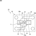
- FIG. 1 is a plan view of an elastic wave device according to a first embodiment of the present invention.
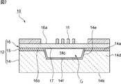
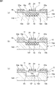
- FIG. 2 is a cross-sectional view of the elastic wave device according to the first embodiment of the present invention, and is a cross-sectional view of a portion along the line I-I of FIG. 3 (a) to 3 (d) are front sectional views for explaining an example of a method for manufacturing an elastic wave device according to a first embodiment of the present invention.
- 4 (a) to 4 (c) are front sectional views for explaining an example of a method for manufacturing an elastic wave device according to a first embodiment of the present invention.
- 5 (a) and 5 (b) are front sectional views for explaining an example of a method for manufacturing an elastic wave device according to a first embodiment of the present invention.
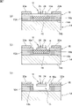
- FIG. 6 (a) to 6 (d) are front sectional views for explaining another example of the method for manufacturing the elastic wave device according to the first embodiment of the present invention.
- 7 (a) to 7 (c) are front sectional views for explaining another example of the method for manufacturing the elastic wave device according to the first embodiment of the present invention.
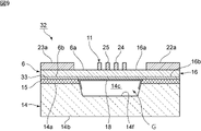
- FIG. 8 is a front sectional view of the elastic wave device according to the second embodiment of the present invention.
- FIG. 9 is a front sectional view of the elastic wave device according to the third embodiment of the present invention.
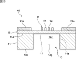
- FIG. 10 is a front sectional view of the elastic wave device according to the fourth embodiment of the present invention.
- FIG. 11 is a front sectional view of the elastic wave device according to the fifth embodiment of the present invention.
- FIG. 12 is a front sectional view of the elastic wave device according to the sixth embodiment of the present invention.
- 13 (a) and 13 (b) are a schematic perspective view showing the appearance of an elastic wave device using a thickness slip mode and a plan view showing an electrode structure on a piezoelectric layer.
- FIG. 14 is a cross-sectional view of a portion along the line AA in FIG. 13 (a).
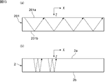
- FIG. 15 (a) is a schematic front sectional view for explaining a ram wave propagating in a piezoelectric film of a conventional elastic wave device, and
- FIG. 15 (b) shows an elastic wave device using a thickness slip mode. It is a schematic front sectional view for demonstrating vibration.
- FIG. 16 is a diagram for explaining the amplitude direction of the bulk wave in the thickness slip mode.
- FIG. 17 is a diagram showing resonance characteristics of an elastic wave device using a thickness slip mode.
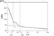
- FIG. 18 is a diagram showing the relationship between d / 2p and the specific band as a resonator when the distance between the centers of adjacent electrode fingers is p and the thickness of the piezoelectric layer is d.
- FIG. 19 is a plan view showing an elastic wave device using a bulk wave in a thickness slip mode.
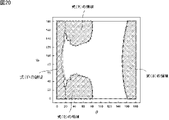
- FIG. 20 is a diagram showing a map of the specific band with respect to Euler angles (0 °, ⁇ , ⁇ ) of LiNbO3 when d / p is brought as close to 0 as possible.
- FIG. 21 is a diagram showing the relationship between d / 2p, the metallization ratio MR, and the specific band.
- FIG. 1 is a plan view of an elastic wave device according to a first embodiment of the present invention.
- FIG. 2 is a cross-sectional view of the elastic wave device according to the first embodiment of the present invention. Note that FIG. 2 is a cross-sectional view of a portion along the line I-I in FIG.
- the elastic wave device 10 has a piezoelectric substrate 12 and an IDT electrode 11 provided on the piezoelectric substrate 12.
- the piezoelectric substrate 12 has a support substrate 14 as a support member, a dielectric layer 15, and a piezoelectric layer 16.
- a piezoelectric layer 16 is provided on the support substrate 14 via the dielectric layer 15.
- the support substrate 14 has a first main surface 14a and a second main surface 14b.
- the first main surface 14a and the second main surface 14b face each other.
- the first main surface 14a is provided with a recess 14c.
- the support substrate 14 has a support portion 14d.
- the support portion 14d is a portion that surrounds the recess 14c and supports the piezoelectric layer 16 via the dielectric layer 15.
- the piezoelectric layer 16 is provided on the dielectric layer 15 so as to close the recess 14c.
- the recess 14c constitutes the air gap portion G.
- the air gap portion G is surrounded by the support substrate 14, the dielectric layer 15, and the piezoelectric layer 16.
- the piezoelectric layer 16 has a first main surface 16a and a second main surface 16b.
- the first main surface 16a and the second main surface 16b face each other.
- the second main surface 16b is the main surface on the support substrate 14 side.
- the piezoelectric layer 16 is made of lithium niobate such as LiNbO 3 or lithium tantalate such as LiTaO 3 .
- the fact that a certain member is made of a certain material includes the case where a trace amount of impurities is contained so as not to deteriorate the electrical characteristics of the elastic wave device.
- the IDT electrode 11 is provided on the first main surface 16a of the piezoelectric layer 16.
- the IDT electrode 11 has a first bus bar 22 and a second bus bar 23, and a plurality of first electrode fingers 24 and a plurality of second electrode fingers 25.
- the first bus bar 22 and the second bus bar 23 face each other.
- the plurality of first electrode fingers 24 are periodically arranged. One end of each of the plurality of first electrode fingers 24 is connected to the first bus bar 22.
- the plurality of second electrode fingers 25 are periodically arranged. One end of each of the plurality of second electrode fingers 25 is connected to the second bus bar 23.
- the plurality of first electrode fingers 24 and the plurality of second electrode fingers 25 are interleaved with each other.
- Wiring electrodes 22a and 23a are provided on the first main surface 16a.
- the wiring electrodes 22a and 23a are electrically connected to the IDT electrode 11.
- the direction in which the adjacent first electrode finger 24 and the second electrode finger 25 face each other is defined as the electrode finger facing direction.
- the electrode finger facing direction is orthogonal to the direction in which the plurality of first electrode fingers 24 and the plurality of second electrode fingers 25 extend.
- the first electrode finger 24 and the second electrode finger 25 may be simply referred to as an electrode finger.
- the air gap portion G may overlap with at least a part of the IDT electrode 11 in the thickness direction of the support member.
- the elastic wave is excited by applying an AC voltage to the IDT electrode 11.
- the elastic wave device 10 is configured to be able to use, for example, a bulk wave in a thickness slip mode.
- the optimum form of the elastic wave device using the bulk wave in this thickness slip mode will be described later with reference to FIGS. 13 and later.
- the support substrate 14 has an inner side wall 14e facing the air gap portion G. Further, in the air gap portion G, the support substrate 14 has a bottom surface 14f facing the piezoelectric layer 16.
- the high thermal conductive film 17 is laminated on the second main surface 16b of the piezoelectric layer 16. The high thermal conductive film 17 is directly laminated on the second main surface 16b. However, the high thermal conductive film 17 may be indirectly laminated on the second main surface 16b.
- the high thermal conductivity film 17 has a higher thermal conductivity than the piezoelectric layer 16.
- the high thermal conductivity film 17 is made of such a material having high thermal conductivity. Examples of the material having a high thermal conductivity include a metal and an insulator having a higher thermal conductivity than a piezoelectric single crystal.
- the high thermal conductive film 17 reaches from the second main surface 16b of the piezoelectric layer 16 to the inner side wall 14e of the support substrate 14, and further, in the present embodiment, the high thermal conductive film 17 reaches on the bottom surface 14f of the recess 14c. It is provided in. That is, in the present embodiment, the high thermal conductive film 17 is provided so as to surround the air gap portion G.
- the heat generated by the excitation is quickly released to the air gap portion G side via the high thermal conductive film 17. Therefore, the heat dissipation can be effectively improved.
- the thermal conductivity of at least one of the support substrate 14 and the dielectric layer 15 is higher than the thermal conductivity of the piezoelectric layer 16.
- the heat dissipation property can be further improved.
- the thermal conductivity of the support substrate 14 is higher than the thermal conductivity of the piezoelectric layer 16. Thereby, the heat dissipation property can be enhanced more effectively.
- the support member is composed of only the support substrate 14, it may have a structure in which another dielectric layer or a semiconductor layer is laminated on the support substrate 14.
- the high thermal conductive film 17 is preferably a dielectric film made of a dielectric having high thermal conductivity as described above.
- the dielectric for example, aluminum oxide, silicon nitride, zirconia, titania, graphene and the like are suitable. More preferably, aluminum oxide, silicon oxide, silicon nitride or silicon oxynitride is used as the dielectric. Thereby, the heat dissipation property can be enhanced more effectively.
- the thickness of the high thermal conductive film 17 may be uniform, but may be partially different. As shown in FIG. 2, the thickness of the high thermal conductive film 17 on the inner side wall 14e and the bottom surface 14f may be thicker than the thickness of the high thermal conductive film 17 on the second main surface 16b of the piezoelectric layer 16. ..
- a recess 14c is formed in the support substrate 14.
- the formation of the recess 14c can be obtained by applying a resist from the first main surface 14a side, patterning, etching the support substrate, and removing the resist.
- the sacrificial layer 18 is provided in the recess 14c.
- the formation of the sacrificial layer 18 can be obtained by forming the sacrificial layer 18 and flattening it by grinding.
- the sacrificial layer 18 is made of a material that is removed in a step described later.
- the dielectric layer 15 is laminated. After laminating the dielectric layer 15, the piezoelectric substrate 16A is bonded onto the dielectric layer 15.
- the piezoelectric substrate 16A is ground.
- the piezoelectric layer 16 shown in FIG. 3D is formed.
- the IDT electrode 11 and the wiring electrodes 22a and 23a are formed by the lift-off method.
- the resist layer To remove After coating and patterning the resist and dry etching the piezoelectric layer 16 and the dielectric layer 15 of the opening H to remove the piezoelectric layer 16 and the dielectric layer 15 located in the opening H described later, the resist layer To remove. As a result, as shown in FIG. 4B, the opening H is formed in the piezoelectric layer 16 and the dielectric layer 15. The opening H is provided to remove the sacrificial layer 18.
- the parts other than the opening H are protected by the resist, and the etching solutions for removing the sacrificial layer 18 and the dielectric layer are injected from the opening H, respectively, and removed, and then the resist is removed. Thereby, as shown in FIG. 4 (c), the sacrificial layer 18 and the dielectric layer 15 are removed. In this way, the air gap portion G is provided.
- a high thermal conductive film 17 is formed.
- This film formation can be performed by a method such as ALD (Atomic Layer Deposition) or CVD.
- ALD Atomic Layer Deposition
- CVD chemical vapor deposition
- the ALD film forming method is used.
- the high thermal conductive film 17 can be formed with a high precision thickness.
- the ALD layer (high thermal conductive film 17) on the IDT electrode 11 and the wiring electrodes 22a and 23a is removed by ion milling. As shown in the figure, the high thermal conductive film 17 may remain on the side wall of the opening H.
- an ion beam such as an Ar beam can be used.
- FIGS. 6 (a) to 6 (d) and FIGS. 7 (a) to 7 (c) another example of the method for manufacturing the elastic wave device 10 of the first embodiment will be described.
- the sacrificial layer 18 is formed on the piezoelectric substrate 16A.
- the sacrificial layer 18 can be formed by applying a resist, patterning, etching the sacrificial layer 18, and removing the resist.
- a dielectric layer 15A is formed as a bonding layer made of a dielectric.
- the dielectric layer 15A is formed, for example, by forming a dielectric layer and then flattening it by grinding.
- the support substrate 14 is laminated on the dielectric layer 15A. That is, by using the dielectric layer 15A as the bonding layer, the piezoelectric substrate 16A and the support substrate 14 can be bonded.
- the piezoelectric substrate 16A is ground and thinned. Thereby, the piezoelectric layer 16 is formed.
- the IDT electrode 11 and the wiring electrodes 22a and 23a are formed.
- the IDT electrode 11 and the wiring electrodes 22a and 23a can be formed by, for example, a lift-off method.
- an opening H is provided.
- the opening H can be formed by applying a resist, patterning, dry etching the piezoelectric layer 16 of the opening H, and removing the resist.
- the sacrificial layer 18 is removed.
- the sacrificial layer 18 can be removed by applying a resist, patterning, removing the sacrificial layer by injecting an etching solution for the sacrificial layer from the opening H, and removing the resist.
- the high thermal conductive film 17 may be formed.
- the method for manufacturing an elastic wave device in the present invention is not limited to the above examples.
- FIG. 8 is a front sectional view of the elastic wave device according to the second embodiment of the present invention.
- the high thermal conductive film 17 is provided so as to extend from the second main surface 16b of the piezoelectric layer 16 to the middle of the inner side wall 14e of the support substrate 14 as a support member. That is, the high thermal conductive film 17 is provided so as not to reach the bottom surface 14f of the recess 14c of the support substrate 14.
- the high thermal conductive film 17 is formed by at least a part of the portion directly or indirectly laminated on the second main surface 16b of the piezoelectric layer 16 and the inner side wall 14e of the support substrate 14 connected to the second main surface 16b. It suffices to have the part provided in. Thereby, the heat dissipation can be effectively improved.
- FIG. 9 is a front sectional view of the elastic wave device according to the third embodiment of the present invention.
- the elastic wave device 32 is provided with an additional film 33. Further, the dielectric layer 15 is provided. In other configurations, the elastic wave device 32 is the same as the elastic wave device 31.
- the additional film 33 is laminated on the entire surface of the second main surface 16b of the piezoelectric layer 16. Then, the piezoelectric layer 16 is laminated on the support substrate 14 via the dielectric layer 15 and the additional film 33.
- the high thermal conductive film 17 is not directly laminated on the second main surface 16b facing the IDT electrode 11. That is, the high thermal conductive film 17 is laminated via the additional film 33 on the portion of the second main surface 16b facing the air gap portion G.
- the additional film 33 Even if the additional film 33 is provided, the heat dissipation can be improved by the high thermal conductive film 17. That is, the additional film 33 may have a lower thermal conductivity than the support member. As the additional film 33, a film made of a material having a higher thermal conductivity than the piezoelectric layer 16 is preferably used.
- the thermal conductivity may be lower than that of the piezoelectric layer 16, and even in that case, since the high thermal conductive film 17 is present on the lower surface, the heat dissipation can be improved. .. As described above, the high thermal conductive film 17 may be indirectly laminated on the second main surface 16b of the piezoelectric layer 16.
- FIG. 10 is a front sectional view of the elastic wave device according to the fourth embodiment of the present invention.
- the piezoelectric layer 16 is directly laminated on the support substrate 14.
- the support member is composed of only the support substrate 14.
- the air gap portion G facing the second main surface of the piezoelectric layer 16 is formed by a through hole 14g provided in the support substrate 14.
- the support substrate 14 may be provided with a through hole 14g penetrating from the first main surface 14a to the second main surface 14b, thereby providing an air gap portion G.
- the high thermal conductive film 17 is provided so as to extend from the second main surface 16b of the piezoelectric layer 16 to the inner side wall 14e of the support substrate 14. As a result, heat dissipation is enhanced.
- FIG. 11 is a front sectional view of the elastic wave device according to the fifth embodiment of the present invention.
- the inner side wall 14e facing the air gap portion G has the convex portion 14e1.
- the high thermal conductive film 17 further reaches the bottom surface 14f so as to cover the uneven portion of the inner side wall 14e.
- the convex portion 14e1 may be provided on the inner side wall 14e of the support substrate 14 at least in a part thereof. In that case, the surface area of the high thermal conductive film 17 increases. Therefore, the heat dissipation can be further improved.
- FIG. 12 is a partially cutaway perspective view for explaining the elastic wave device according to the sixth embodiment of the present invention.
- the elastic wave device 81 has a support substrate 82.
- the support substrate 82 is provided with a recess opened on the upper surface.
- the piezoelectric layer 83 is laminated on the support substrate 82.
- the air gap portion 9 is configured.
- An IDT electrode 84 is provided on the piezoelectric layer 83 above the air gap portion 9. Reflectors 85 and 86 are provided on both sides of the IDT electrode 84 in the elastic wave propagation direction. In FIG. 12, the outer peripheral edge of the air gap portion 9 is shown by a broken line.
- the IDT electrode 84 has first and second bus bars 84a and 84b, a plurality of electrodes 84c as first electrode fingers, and a plurality of electrodes 84d as second electrode fingers.
- the plurality of electrodes 84c are connected to the first bus bar 84a.
- the plurality of electrodes 84d are connected to the second bus bar 84b.
- the plurality of electrodes 84c and the plurality of electrodes 84d are interleaved with each other.
- a high thermal conductive film 87 is provided so as to extend from below the piezoelectric layer 83 to the inner side wall of the recess.
- the elastic wave device 81 a lamb wave as a plate wave is excited by applying an AC electric field to the IDT electrode 84 on the air gap portion 9. Since the reflectors 85 and 86 are provided on both sides, the resonance characteristic due to the Lamb wave can be obtained. As described above, the elastic wave device of the present invention may utilize a plate wave.
- the support member in the following example corresponds to the support substrate in the present invention.
- FIG. 13 (a) is a schematic perspective view showing the appearance of an elastic wave device using a bulk wave in a thickness slip mode
- FIG. 13 (b) is a plan view showing an electrode structure on a piezoelectric layer
- FIG. 14 is a cross-sectional view of a portion along the line AA in FIG. 13 (a).
- the elastic wave device 1 has a piezoelectric layer 2 made of LiNbO 3 .
- the piezoelectric layer 2 may be made of LiTaO 3 .
- the cut angle of LiNbO 3 and LiTaO 3 is Z-cut, but may be rotary Y-cut or X-cut.
- the thickness of the piezoelectric layer 2 is not particularly limited, but in order to effectively excite the thickness slip mode, it is preferably 40 nm or more and 1000 nm or less, and more preferably 50 nm or more and 1000 nm or less.
- the piezoelectric layer 2 has first and second main surfaces 2a and 2b facing each other. An electrode finger 3 and an electrode finger 4 are provided on the first main surface 2a. In FIGS.
- a plurality of electrode fingers 3 are connected to the first bus bar 5.
- the plurality of electrode fingers 4 are connected to the second bus bar 6.
- the plurality of electrode fingers 3 and the plurality of electrode fingers 4 are interleaved with each other.
- the electrode finger 3 and the electrode finger 4 have a rectangular shape and have a length direction.
- the electrode finger 3 and the adjacent electrode finger 4 face each other in a direction orthogonal to the length direction. Both the length direction of the electrode fingers 3 and 4 and the direction orthogonal to the length direction of the electrode fingers 3 and 4 are directions intersecting with each other in the thickness direction of the piezoelectric layer 2.
- the electrode finger 3 and the adjacent electrode finger 4 face each other in the direction of crossing in the thickness direction of the piezoelectric layer 2.
- the length directions of the electrode fingers 3 and 4 may be interchanged with the directions orthogonal to the length directions of the electrode fingers 3 and 4 shown in FIGS. 13 (a) and 13 (b). That is, in FIGS. 13 (a) and 13 (b), the electrode fingers 3 and 4 may be extended in the direction in which the first bus bar 5 and the second bus bar 6 are extended. In that case, the first bus bar 5 and the second bus bar 6 extend in the direction in which the electrode fingers 3 and 4 extend in FIGS. 13 (a) and 13 (b).
- a pair of structures in which the electrode finger 3 connected to one potential and the electrode finger 4 connected to the other potential are adjacent to each other are paired in a direction orthogonal to the length direction of the electrode fingers 3 and 4. It is provided.
- the fact that the electrode finger 3 and the electrode finger 4 are adjacent to each other does not mean that the electrode finger 3 and the electrode finger 4 are arranged so as to be in direct contact with each other, but that the electrode finger 3 and the electrode finger 4 are placed next to each other through a gap. Refers to the case where they are arranged.
- an electrode connected to a hot electrode or a ground electrode including other electrode fingers 3 and 4 is arranged between the electrode finger 3 and the electrode finger 4. Not done.
- This logarithm does not have to be an integer pair, and may be 1.5 pairs, 2.5 pairs, or the like.
- the distance between the centers of the electrode fingers 3 and 4, that is, the pitch is preferably in the range of 1 ⁇ m or more and 10 ⁇ m or less.
- the width of the electrode fingers 3 and 4, that is, the dimensions of the electrode fingers 3 and 4 in the opposite direction are preferably in the range of 50 nm or more and 1000 nm or less, and more preferably in the range of 150 nm or more and 1000 nm or less.
- the distance between the centers of the electrode fingers 3 and 4 is orthogonal to the center of the dimension (width dimension) of the electrode finger 3 in the direction orthogonal to the length direction of the electrode finger 3 and the length direction of the electrode finger 4. It is the distance connected to the center of the dimension (width dimension) of the electrode finger 4 in the direction.
- the direction orthogonal to the length direction of the electrode fingers 3 and 4 is the direction orthogonal to the polarization direction of the piezoelectric layer 2. This does not apply when a piezoelectric material having another cut angle is used as the piezoelectric layer 2.
- “orthogonal” is not limited to the case of being strictly orthogonal, and is substantially orthogonal (the angle formed by the direction orthogonal to the length direction of the electrode fingers 3 and 4 and the polarization direction is, for example, 90 ° ⁇ 10 °). Within the range of).
- a support member 8 is laminated on the second main surface 2b side of the piezoelectric layer 2 via an insulating layer 7.
- the insulating layer 7 and the support member 8 have a frame-like shape and have openings 7a and 8a as shown in FIG.
- the air gap portion 9 is provided so as not to interfere with the vibration of the excitation region C of the piezoelectric layer 2. Therefore, the support member 8 is laminated on the second main surface 2b via the insulating layer 7 at a position where it does not overlap with the portion where at least one pair of electrode fingers 3 and 4 are provided.
- the insulating layer 7 may not be provided. Therefore, the support member 8 may be directly or indirectly laminated on the second main surface 2b of the piezoelectric layer 2.
- the insulating layer 7 is made of silicon oxide. However, in addition to silicon oxide, an appropriate insulating material such as silicon nitride or alumina can be used.
- the support member 8 is made of Si. The plane orientation of Si on the surface of the piezoelectric layer 2 side may be (100), (110), or (111). It is desirable that Si constituting the support member 8 has a high resistance having a resistivity of 4 k ⁇ or more. However, the support member 8 can also be configured by using an appropriate insulating material or semiconductor material.
- Examples of the material of the support member 8 include piezoelectric materials such as aluminum oxide, lithium tantalate, lithium niobate, and quartz, alumina, magnesia, sapphire, silicon nitride, aluminum nitride, silicon carbide, zirconia, cordierite, mulite, and steer.
- piezoelectric materials such as aluminum oxide, lithium tantalate, lithium niobate, and quartz, alumina, magnesia, sapphire, silicon nitride, aluminum nitride, silicon carbide, zirconia, cordierite, mulite, and steer.
- Various ceramics such as tight and forsterite, dielectrics such as diamond and glass, and semiconductors such as gallium nitride can be used.
- the plurality of electrode fingers 3 and 4 and the first and second bus bars 5 and 6 are made of an appropriate metal or alloy such as Al or AlCu alloy.
- the electrode fingers 3 and 4 and the first and second bus bars 5 and 6 have a structure in which an Al film is laminated on a Ti film.
- An adhesive layer other than the Ti film may be used.
- an AC voltage is applied between the plurality of electrode fingers 3 and the plurality of electrode fingers 4. More specifically, an AC voltage is applied between the first bus bar 5 and the second bus bar 6.
- d / p is It is said to be 0.5 or less. Therefore, the bulk wave in the thickness slip mode is effectively excited, and good resonance characteristics can be obtained. More preferably, d / p is 0.24 or less, in which case even better resonance characteristics can be obtained.
- the Q value is unlikely to decrease even if the logarithm of the electrode fingers 3 and 4 is reduced in order to reduce the size. This is because the propagation loss is small even if the number of electrode fingers in the reflectors on both sides is reduced. Further, the reason why the number of the electrode fingers can be reduced is that the bulk wave in the thickness slip mode is used. The difference between the lamb wave used in the elastic wave device and the bulk wave in the thickness slip mode will be described with reference to FIGS. 15 (a) and 15 (b).
- FIG. 15A is a schematic front sectional view for explaining a Lamb wave propagating in a piezoelectric film of an elastic wave device as described in Patent Document 1.
- the wave propagates in the piezoelectric film 201 as shown by an arrow.
- the first main surface 201a and the second main surface 201b face each other, and the thickness direction connecting the first main surface 201a and the second main surface 201b is the Z direction.
- the X direction is the direction in which the electrode fingers of the IDT electrodes are lined up.
- the wave propagates in the X direction as shown in the figure.
- the piezoelectric film 201 vibrates as a whole because it is a plate wave, the wave propagates in the X direction, so reflectors are arranged on both sides to obtain resonance characteristics. Therefore, a wave propagation loss occurs, and the Q value decreases when the size is reduced, that is, when the logarithm of the electrode fingers is reduced.
- the wave is generated by the first main surface 2a and the second main surface of the piezoelectric layer 2. It propagates substantially in the direction connecting 2b, that is, in the Z direction, and resonates. That is, the X-direction component of the wave is significantly smaller than the Z-direction component. Since the resonance characteristic is obtained by the propagation of the wave in the Z direction, the propagation loss is unlikely to occur even if the number of electrode fingers of the reflector is reduced. Further, even if the logarithm of the electrode fingers composed of the electrode fingers 3 and 4 is reduced in order to promote miniaturization, the Q value is unlikely to decrease.
- the amplitude direction of the bulk wave in the thickness slip mode is opposite in the first region 451 included in the excitation region C of the piezoelectric layer 2 and the second region 452 included in the excitation region C.
- FIG. 16 schematically shows a bulk wave when a voltage is applied between the electrode finger 3 and the electrode finger 4 so that the electrode finger 4 has a higher potential than the electrode finger 3.
- the first region 451 is a region of the excitation region C between the virtual plane VP1 orthogonal to the thickness direction of the piezoelectric layer 2 and dividing the piezoelectric layer 2 into two, and the first main surface 2a.
- the second region 452 is a region of the excitation region C between the virtual plane VP1 and the second main surface 2b.
- the elastic wave device 1 at least one pair of electrodes consisting of the electrode finger 3 and the electrode finger 4 is arranged, but since the wave is not propagated in the X direction, the electrode fingers 3 and 3 are arranged.
- the number of pairs of electrode fingers consisting of 4 does not have to be multiple. That is, it is only necessary to provide at least one pair of electrodes.
- the electrode finger 3 is an electrode connected to a hot potential
- the electrode finger 4 is an electrode connected to a ground potential.
- the electrode finger 3 may be connected to the ground potential and the electrode finger 4 may be connected to the hot potential.
- at least one pair of electrodes is an electrode connected to a hot potential or an electrode connected to a ground potential as described above, and is not provided with a floating electrode.
- FIG. 17 is a diagram showing the resonance characteristics of the elastic wave device shown in FIG.
- the design parameters of the elastic wave device 1 that has obtained this resonance characteristic are as follows.
- Insulation layer 7 1 ⁇ m thick silicon oxide film.
- Support member 8 Si.
- the length of the excitation region C is a dimension along the length direction of the electrode fingers 3 and 4 of the excitation region C.
- the distances between the electrode fingers of the electrode finger pairs consisting of the electrode fingers 3 and 4 are all the same in the plurality of pairs. That is, the electrode fingers 3 and the electrode fingers 4 were arranged at equal pitches.
- d / p is 0.5 or less. More preferably, it is 0.24 or less. This will be described with reference to FIG.
- FIG. 18 is a diagram showing the relationship between this d / 2p and the specific band as a resonator of the elastic wave device.
- the ratio band is less than 5% even if d / p is adjusted.
- the specific band can be set to 5% or more by changing d / p within that range. That is, a resonator having a high coupling coefficient can be constructed.
- the specific band can be increased to 7% or more.
- a resonator having a wider specific band can be obtained, and a resonator having a higher coupling coefficient can be realized. Therefore, it can be seen that by setting d / p to 0.5 or less, a resonator having a high coupling coefficient can be configured by utilizing the bulk wave in the thickness slip mode.
- FIG. 19 is a plan view of an elastic wave device that utilizes bulk waves in a thickness slip mode.
- the elastic wave device 80 a pair of electrodes having an electrode finger 3 and an electrode finger 4 is provided on the first main surface 2a of the piezoelectric layer 2.
- K in FIG. 19 is the crossover width.
- the logarithm of the electrode fingers may be one pair. Even in this case, if the d / p is 0.5 or less, the bulk wave in the thickness slip mode can be effectively excited.
- FIG. 20 is a diagram showing a map of the specific band with respect to Euler angles (0 °, ⁇ , ⁇ ) of LiNbO3 when d / p is brought as close to 0 as possible.
- the portion shown with hatching in FIG. 20 is a region where a specific band of at least 5% or more can be obtained, and when the range of the region is approximated, the following equations (1), (2) and (3) are approximated. ).
- Equation (1) (0 ° ⁇ 10 °, 20 ° to 80 °, 0 ° to 60 ° (1- ( ⁇ -50) 2/900) 1/2) or (0 ° ⁇ 10 °, 20 ° to 80 °, [180] ° -60 ° (1- ( ⁇ -50) 2/900) 1/2] to 180 °).
- Equation (2) (0 ° ⁇ 10 °, [180 ° -30 ° (1- ( ⁇ -90) 2/8100) 1/2] to 180 °, arbitrary ⁇ ).
- the specific band can be sufficiently widened, which is preferable.
- the piezoelectric layer 2 is a lithium tantalate layer.
- FIG. 21 is a diagram showing the relationship between d / 2p, the metallization ratio MR, and the specific band.
- various elastic wave devices having different MRs from d / 2p were configured, and the specific band was measured.
- the portion shown with hatching on the right side of the broken line E in FIG. 21 is a region having a specific band of 17% or less.
- the spurious can be suitably reduced by adjusting the film thickness of the piezoelectric layer 2 and the dimensions of the electrode fingers 3 and 4.
- MR 1.75 (d / p) +0.075. Therefore, MR ⁇ 1.75 (d / p) +0.075 is preferable.
- Piezoelectric wave device 2 ... Piezoelectric layer 2a ... First main surface 2b ... Second main surface 3,4 ... Electrode fingers 5, 6 ... First, second bus bar 7 ... Insulation layer 7a ... Opening 8 ... Support member 8a ... Opening 9 ... Air gap 10 ... Elastic wave device 11 ... IDT electrode 12 ... Piezoelectric substrate 14 ... Support substrate 14a, 14b ... First and second main surfaces 14c ... Recess 14d ... Support portion 14e ... Inner side wall 14e1 ... Convex portion 14f ... Bottom surface 14g ... Through holes 15, 15A ... Dielectric layer 16 ... Piezoelectric layer 16A ... Piezoelectric substrate 16a, 16b ... First and second main surfaces 17 ...
- High thermal conductive film 18 ... Sacrificial layer 22 , 23 ... 1st and 2nd bus bars 22a, 23a ... Wiring electrodes 24, 25 ... 1st and 2nd electrode fingers 31, 32 ... Elastic wave device 33 ... Additional film 40, 50, 80, 81 ... Elastic wave device 82 ... Support substrate 83 ... Piezoelectric layer 84 ... IDT electrodes 84a, 84b ... First and second bus bars 84c, 84d ... Electrodes 85, 86 ... Reflector 87 ... High thermal conductivity film 201 ... Piezoelectric film 201a, 201b ... First 1, 2nd main surface 451 and 452 ... 1st and 2nd regions C ... Excitation region D ... Crossing region G ... Air gap portion H ... Opening VP1 ... Virtual plane
Landscapes
- Physics & Mathematics (AREA)
- Acoustics & Sound (AREA)
- Engineering & Computer Science (AREA)
- Manufacturing & Machinery (AREA)
- General Physics & Mathematics (AREA)
- Chemical & Material Sciences (AREA)
- Crystallography & Structural Chemistry (AREA)
- Spectroscopy & Molecular Physics (AREA)
- Ceramic Engineering (AREA)
- Surface Acoustic Wave Elements And Circuit Networks Thereof (AREA)
Abstract
放熱性に優れた、弾性波装置を提供する。 支持基板14を含む支持部材と、支持部材上に設けられている圧電層16と、圧電層16の第1の主面16aに設けられたIDT電極11と、を備え、支持部材に、圧電層16側に開口しているエアギャップ部14cが設けられており、支持部材14が、エアギャップ部14cに面している内側壁14eを有し、高熱伝導膜17が、圧電層16の第2の主面16bの少なくとも一部に直接または間接に積層されており、さらに支持部材14の内側壁14eに至っている、弾性波装置10。
Description
本発明は、ニオブ酸リチウムまたはタンタル酸リチウムからなる圧電層を有する弾性波装置に関する。
従来、ニオブ酸リチウムやタンタル酸リチウムからなる圧電層を有する弾性波装置が知られている。例えば、下記の特許文献1では、キャビティを有する支持基板上に、ニオブ酸リチウムまたはタンタル酸リチウムからなる圧電層を設けた弾性波装置が開示されている。この弾性波装置では、キャビティの上方において、圧電層の上面にIDT電極が設けられている。
特許文献1に記載のような従来の弾性波装置では、放熱性の改善が求められている。
本発明の目的は、放熱性に優れた弾性波装置を提供することにある。
本発明は、支持基板を含む支持部材と、前記支持部材上に設けられており、対向し合う第1,第2の主面を有する圧電層と、前記圧電層の前記第1の主面に設けられており、複数本の電極指を有するIDT電極と、を備え、前記支持部材に、前記圧電層側に開口しているエアギャップ部が設けられており、前記エアギャップ部が、前記支持部材の厚み方向において、前記IDT電極の少なくとも一部と重なっており、前記支持部材が、前記エアギャップ部に面している内側壁を有し、前記圧電層の前記第2の主面の少なくとも一部に直接または間接に積層されており、さらに前記支持部材の前記内側壁に至っており、前記圧電層よりも熱伝導率の高い高熱伝導膜をさらに備える。
本発明によれば、放熱性に優れた弾性波装置を提供することができる。
以下、図面を参照しつつ、本発明の具体的な実施形態を説明することにより、本発明を明らかにする。
図1は、本発明の第1の実施形態に係る弾性波装置の平面図である。図2は、本発明の第1の実施形態の弾性波装置の断面図である。なお、図2は、図1中のI-I線に沿う部分の断面図である。
図2に示すように、弾性波装置10は、圧電性基板12と、圧電性基板12上に設けられたIDT電極11とを有する。圧電性基板12は、支持部材としての支持基板14と、誘電体層15と、圧電層16とを有する。支持基板14上に、誘電体層15を介して、圧電層16が設けられている。
支持基板14は第1の主面14a及び第2の主面14bを有する。第1の主面14a及び第2の主面14bは互いに対向している。第1の主面14aには凹部14cが設けられている。さらに、支持基板14は支持部14dを有する。支持部14dは、凹部14cを囲んでおり、かつ誘電体層15を介して圧電層16を支持している部分である。
圧電層16は、凹部14cを塞ぐように、誘電体層15上に設けられている。本実施形態では、この凹部14cが、エアギャップ部Gを構成している。エアギャップ部Gは、支持基板14、誘電体層15及び圧電層16により囲まれている。
圧電層16は、第1の主面16a及び第2の主面16bを有する。第1の主面16a及び第2の主面16bは互いに対向している。第1の主面16a及び第2の主面16bのうち第2の主面16bが支持基板14側の主面である。
圧電層16は、LiNbO3などのニオブ酸リチウム、またはLiTaO3などのタンタル酸リチウムからなる。なお、本明細書において、ある部材がある材料からなるとは、弾性波装置の電気的特性が劣化しない程度の微量な不純物が含まれる場合を含む。
図1に示すように、圧電層16の第1の主面16aにIDT電極11が設けられている。IDT電極11は、第1のバスバー22及び第2のバスバー23と、複数の第1の電極指24及び複数の第2の電極指25とを有する。第1のバスバー22及び第2のバスバー23は互いに対向している。複数の第1の電極指24は周期的に配置されている。複数の第1の電極指24の一端はそれぞれ、第1のバスバー22に接続されている。複数の第2の電極指25は周期的に配置されている。複数の第2の電極指25の一端はそれぞれ、第2のバスバー23に接続されている。複数の第1の電極指24及び複数の第2の電極指25は互いに間挿し合っている。第1の主面16aには、配線電極22a,23aが設けられている。配線電極22a,23aは、IDT電極11に電気的に接続されている。
隣り合う第1の電極指24及び第2の電極指25が互いに対向する方向を電極指対向方向とする。本実施形態では、電極指対向方向は、複数の第1の電極指24及び複数の第2の電極指25が延びる方向と直交している。以下においては、第1の電極指24及び第2の電極指25を単に電極指と記載することがある。
なお、エアギャップ部Gは、支持部材の厚み方向で、IDT電極11の少なくとも一部と重なっておればよい。
弾性波装置10では、IDT電極11に交流電圧を印加することにより、弾性波が励振される。弾性波装置10は、例えば厚み滑りモードのバルク波を利用可能なように構成されている。この厚み滑りモードのバルク波を利用した弾性波装置の最適な形態については、図13以降を参照して後述する。
図1に示すように、弾性波装置10では、支持基板14が、エアギャップ部Gに面している内側壁14eを有する。また、エアギャップ部Gにおいて、支持基板14は、圧電層16に対向している底面14fを有する。エアギャップ部Gにおいて、圧電層16の第2の主面16bに高熱伝導膜17が積層されている。高熱伝導膜17は、第2の主面16bに直接積層されている。もっとも、第2の主面16bに間接に高熱伝導膜17が積層されていてもよい。
高熱伝導膜17は、圧電層16よりも熱伝導率が高い。このような熱伝導率の高い材料により、高熱伝導膜17が構成されている。熱伝導率が高い材料としては、金属、圧電単結晶よりも熱伝導率が高い絶縁体などを挙げることができる。
高熱伝導膜17は、圧電層16の第2の主面16bから支持基板14の内側壁14eに至っており、さらに、本実施形態では、高熱伝導膜17は、凹部14cの底面14f上に至るように設けられている。すなわち、本実施形態では、高熱伝導膜17は、エアギャップ部Gを取り囲むように設けられている。
従来、エアギャップ部の上方に、圧電層が設けられている構造では、励振により生じた熱が、圧電層から外部に逃がされにくいという問題があった。より具体的には、IDT電極を駆動すると、圧電層のIDT電極が設けられている領域において、熱が発生する。ところが、圧電層の下方にエアギャップ部が存在すると、発生した熱が逃がされがたい。すなわち、放熱性が低いという問題があった。
これに対して、弾性波装置10では、上記高熱伝導膜17が設けられているため、励振により生じた熱が、高熱伝導膜17を介してエアギャップ部G側に速やかに逃がされる。従って、放熱性を効果的に高めることができる。
好ましくは、支持基板14及び誘電体層15の少なくとも一方の熱伝導率は、圧電層16の熱伝導率よりも高い。それによって、放熱性をより一層高めることができる。
支持基板14の熱伝導率が、圧電層16の熱伝導率よりも高いことが好ましい。それによって、放熱性をより効果的に高めることができる。
なお、支持部材は、支持基板14のみにより構成されているが、支持基板14に、他の誘電体層や半導体層が積層されている構造を有していてもよい。
高熱伝導膜17は、好ましくは、上記のような熱伝導性が高い誘電体からなる誘電体膜である。誘電体としては、例えば、酸化アルミニウム、窒化ケイ素、ジルコニア、チタニアまたはグラフェンなどが好適である。上記誘電体としては、より好ましくは、酸化アルミニウム、酸化ケイ素、窒化ケイ素または酸窒化ケイ素が用いられる。それによって、放熱性をより効果的に高めることができる。
高熱伝導膜17の厚みは、均一でもよいが、部分的に異なっていてもよい。図2に示すように、圧電層16の第2の主面16b上における高熱伝導膜17の厚みよりも、内側壁14e上及び底面14f上における高熱伝導膜17の厚みが厚くされていてもよい。
図3(a)~(d)及び図4(a)~図4(c)、並びに図5(a)及び図5(b)を参照して弾性波装置10の製造方法の一例を説明する。
まず、図3(a)に示すように、支持基板14に、凹部14cを形成する。この凹部14cの形成は、第1の主面14a側からレジストの付与、パターニング、支持基板のエッチング及びレジストの除去により得ることができる。
次に、図3(b)に示すように、凹部14cに、犠牲層18を設ける。この犠牲層18の形成は、犠牲層18の成膜、及び研削での平坦化により得ることができる。犠牲層18は、後述する工程で除去される材料からなる。
次に、図3(c)に示すように、誘電体層15を積層する。誘電体層15を積層したのちに、誘電体層15上に、圧電基板16Aを接合する。
次に、圧電基板16Aを研削する。それによって、図3(d)に示す圧電層16を形成する。
次に、図4(a)に示すように、リフトオフ法により、IDT電極11及び配線電極22a,23aを形成する。
レジストの塗布、パターニング及び開口部Hの圧電体層16と誘電体層15をドライエッチングして後述の開口部Hに位置している圧電体層16と誘電体層15を除去したのち、レジスト層を除去する。それによって、図4(b)に示すように、開口部Hを圧電層16と誘電体層15に形成する。開口部Hは、犠牲層18を除去するために設けられている。
レジスト塗布、パターニングにより開口部H以外をレジストで保護し、開口部Hから犠牲層18と誘電体層を除去するためのそれぞれエッチング液を注入し、除去し、その後、レジストを除去する。それによって、図4(c)に示すように、犠牲層18と誘電体層15とを除去する。このようにして、エアギャップ部Gが設けられる。
次に、図5(a)に示すように、高熱伝導膜17を成膜する。この成膜は、ALD(Atomic Layer Deposition)またはCVDなどの方法により行うことができる。好ましくは、ALD成膜法が用いられる。それによって、高熱伝導膜17を高精度の厚みにて形成することができる。
次に、図5(b)に示すように、イオンミリングにより、IDT電極11や配線電極22a,23a上のALD層(高熱伝導膜17)を除去する。図示のように、開口部Hの側壁に、高熱伝導膜17が残存していてもよい。
なお、イオンミリングに際しては、Arビームなどのイオンビームを用いることができる。
図6(a)~図6(d)及び図7(a)~図7(c)を参照して、第1の実施形態の弾性波装置10の製造方法の他の例を説明する。
まず、図6(a)に示すように、圧電基板16A上に、犠牲層18を形成する。犠牲層18は、レジストの塗布、パターニング、犠牲層18のエッチング及びレジストの除去により形成することができる。
次に、図6(b)に示すように、誘電体からなる接合層としての誘電体層15Aを形成する。誘電体層15Aは、例えば、誘電体層を成膜後、研削により平坦化して形成する。
次に、図6(c)に示すように、誘電体層15A上に、支持基板14を積層する。すなわち、接合層としての誘電体層15Aを用いることにより、圧電基板16Aと、支持基板14とを接合することができる。
次に、図6(d)に示すように、圧電基板16Aを研削し、薄くする。それによって、圧電層16を形成する。
次に、図7(a)に示すように、IDT電極11及び配線電極22a,23aを形成する。IDT電極11及び配線電極22a,23aは、例えば、リフトオフ法により形成することができる。
次に、図7(b)に示すように、開口部Hを設ける。開口部Hは、レジストの塗布、パターニング、開口部Hの圧電体層16のドライエッチング及びレジストの除去により形成することができる。
次に、図7(c)に示すように、犠牲層18を除去する。犠牲層18の除去は、レジストの塗布、パターニング、開口部Hからの犠牲層のエッチング液の注入による犠牲層の除去及びレジストの除去により行うことができる。
しかる後、図5(a)及び図5(b)に示したように、高熱伝導膜17を形成すればよい。
なお、本発明における弾性波装置の製造方法は上記各例に限定されない。
図8は、本発明の第2の実施形態に係る弾性波装置の正面断面図である。弾性波装置31では、高熱伝導膜17が圧電層16の第2の主面16b上から、支持部材としての支持基板14の内側壁14eの途中に至るように設けられている。すなわち、高熱伝導膜17は、支持基板14の凹部14cの底面14fには至らないように設けられている。このように、高熱伝導膜17は、圧電層16の第2の主面16bに直接または間接に積層された部分と、第2の主面16bに連なる支持基板14の内側壁14eの少なくとも一部に設けられていた部分とを有してさえおればよい。それによって、放熱性を効果的に高めることができる。
図9は、本発明の第3の実施形態に係る弾性波装置の正面断面図である。弾性波装置32では、付加膜33が設けられている。また、誘電体層15が設けられている。その他の構成は、弾性波装置32は弾性波装置31と同様である。付加膜33は、圧電層16の第2の主面16bの全面に積層されている。そして、支持基板14に対して、誘電体層15及び付加膜33を介して圧電層16が積層されている。
高熱伝導膜17は、IDT電極11と対向している第2の主面16b上に直接積層されていない。すなわち、高熱伝導膜17は、第2の主面16bのエアギャップ部Gに面している部分上において、付加膜33を介して積層されている。
付加膜33が設けられていても、高熱伝導膜17により、放熱性を高めることができる。すなわち、付加膜33は支持部材よりも熱伝導率が低くてもよい。付加膜33としては、好ましくは、圧電層16よりも熱伝導率が高い材料からなる膜が用いられる。
もっとも、付加膜33の厚みが薄ければ、熱伝導率は圧電層16より低くてもよく、その場合であっても、下面に高熱伝導膜17が存在するため、放熱性を高めることができる。このように、高熱伝導膜17は、圧電層16の第2の主面16bに間接に積層されていてもよい。
図10は、本発明の第4の実施形態に係る弾性波装置の正面断面図である。弾性波装置40では、支持基板14上に、直接圧電層16が積層されている。また、支持部材は支持基板14のみからなる。そして、圧電層16の第2の主面に臨むエアギャップ部Gは、支持基板14に設けられた貫通孔14gにより形成されている。このように、支持基板14において、第1の主面14aから第2の主面14bに貫通している貫通孔14gを設け、それによってエアギャップ部Gを設けてもよい。
弾性波装置40において、高熱伝導膜17が、圧電層16の第2の主面16bから支持基板14の内側壁14eに至るように設けられている。それによって、放熱性が高められている。
図11は、本発明の第5の実施形態に係る弾性波装置の正面断面図である。弾性波装置50では、支持基板14において、エアギャップ部Gに面している内側壁14eが、凸部14e1を有する。高熱伝導膜17は、内側壁14eの凹凸部を覆うように、さらに底面14fに至っている。このように、支持基板14の内側壁14eに、少なくとも一部に、凸部14e1を設けてもよい。その場合には、高熱伝導膜17の表面積が増加する。そのため、放熱性をより一層高めることができる。
図12は、本発明の第6の実施形態に係る弾性波装置を説明するための部分切り欠き斜視図である。
弾性波装置81は、支持基板82を有する。支持基板82には、上面に開いた凹部が設けられている。支持基板82上に圧電層83が積層されている。それによって、エアギャップ部9が構成されている。このエアギャップ部9の上方において圧電層83上に、IDT電極84が設けられている。IDT電極84の弾性波伝搬方向両側に、反射器85,86が設けられている。図12において、エアギャップ部9の外周縁を破線で示す。ここでは、IDT電極84は、第1,第2のバスバー84a,84bと、複数本の第1の電極指としての電極84c及び複数本の第2の電極指としての電極84dとを有する。複数本の電極84cは、第1のバスバー84aに接続されている。複数本の電極84dは、第2のバスバー84bに接続されている。複数本の電極84cと、複数本の電極84dとは間挿し合っている。
エアギャップ部9において、圧電層83の下方から凹部の内側壁に至るように、高熱伝導膜87が設けられている。
弾性波装置81では、上記エアギャップ部9上のIDT電極84に、交流電界を印加することにより、板波としてのラム波が励振される。そして、反射器85,86が両側に設けられているため、上記ラム波による共振特性を得ることができる。このように、本発明の弾性波装置は、板波を利用するものであってもよい。
以下、本発明の弾性波装置が好適に用いられる、厚み滑りモードのバルク波を利用した弾性波装置について説明する。以下の例における支持部材は、本発明における支持基板に相当する。
図13(a)は、厚み滑りモードのバルク波を利用する弾性波装置の外観を示す略図的斜視図であり、図13(b)は、圧電層上の電極構造を示す平面図であり、図14は、図13(a)中のA-A線に沿う部分の断面図である。
弾性波装置1は、LiNbO3からなる圧電層2を有する。圧電層2は、LiTaO3からなるものであってもよい。LiNbO3やLiTaO3のカット角は、Zカットであるが、回転YカットやXカットであってもよい。圧電層2の厚みは、特に限定されないが、厚み滑りモードを効果的に励振するには、40nm以上、1000nm以下であることが好ましく、50nm以上、1000nm以下であることがより好ましい。圧電層2は、対向し合う第1,第2の主面2a,2bを有する。第1の主面2a上に、電極指3及び電極指4が設けられている。図13(a)及び図13(b)では、複数の電極指3が、第1のバスバー5に接続されている。複数の電極指4は、第2のバスバー6に接続されている。複数の電極指3及び複数の電極指4は、互いに間挿し合っている。電極指3及び電極指4は、矩形形状を有し、長さ方向を有する。この長さ方向と直交する方向において、電極指3と、隣りの電極指4とが対向している。電極指3,4の長さ方向、及び、電極指3,4の長さ方向と直交する方向はいずれも、圧電層2の厚み方向に交叉する方向である。このため、電極指3と、隣りの電極指4とは、圧電層2の厚み方向に交叉する方向において対向しているともいえる。また、電極指3,4の長さ方向が図13(a)及び図13(b)に示す電極指3,4の長さ方向に直交する方向と入れ替わってもよい。すなわち、図13(a)及び図13(b)において、第1のバスバー5及び第2のバスバー6が延びている方向に電極指3,4を延ばしてもよい。その場合、第1のバスバー5及び第2のバスバー6は、図13(a)及び図13(b)において電極指3,4が延びている方向に延びることとなる。そして、一方電位に接続される電極指3と、他方電位に接続される電極指4とが隣り合う1対の構造が、上記電極指3,4の長さ方向と直交する方向に、複数対設けられている。ここで電極指3と電極指4とが隣り合うとは、電極指3と電極指4とが直接接触するように配置されている場合ではなく、電極指3と電極指4とが間隔を介して配置されている場合を指す。また、電極指3と電極指4とが隣り合う場合、電極指3と電極指4との間には、他の電極指3,4を含む、ホット電極やグラウンド電極に接続される電極は配置されない。この対数は、整数対である必要はなく、1.5対や2.5対などであってもよい。電極指3,4間の中心間距離すなわちピッチは、1μm以上、10μm以下の範囲が好ましい。また、電極指3,4の幅、すなわち電極指3,4の対向方向の寸法は、50nm以上、1000nm以下の範囲であることが好ましく、150nm以上、1000nm以下の範囲であることがより好ましい。なお、電極指3,4間の中心間距離とは、電極指3の長さ方向と直交する方向における電極指3の寸法(幅寸法)の中心と、電極指4の長さ方向と直交する方向における電極指4の寸法(幅寸法)の中心とを結んだ距離となる。
また、弾性波装置1では、Zカットの圧電層を用いているため、電極指3,4の長さ方向と直交する方向は、圧電層2の分極方向に直交する方向となる。圧電層2として他のカット角の圧電体を用いた場合には、この限りでない。ここにおいて、「直交」とは、厳密に直交する場合のみに限定されず、略直交(電極指3,4の長さ方向と直交する方向と分極方向とのなす角度が例えば90°±10°の範囲内)でもよい。
圧電層2の第2の主面2b側には、絶縁層7を介して支持部材8が積層されている。絶縁層7及び支持部材8は、枠状の形状を有し、図14に示すように、開口部7a,8aを有する。それによって、エアギャップ部9は、圧電層2の励振領域Cの振動を妨げないために設けられている。従って、上記支持部材8は、少なくとも1対の電極指3,4が設けられている部分と重ならない位置において、第2の主面2bに絶縁層7を介して積層されている。なお、絶縁層7は設けられずともよい。従って、支持部材8は、圧電層2の第2の主面2bに直接または間接に積層され得る。
絶縁層7は、酸化ケイ素からなる。もっとも、酸化ケイ素の他、酸窒化ケイ素、アルミナなどの適宜の絶縁性材料を用いることができる。支持部材8は、Siからなる。Siの圧電層2側の面における面方位は(100)や(110)であってもよく、(111)であってもよい。支持部材8を構成するSiは、抵抗率4kΩ以上の高抵抗であることが望ましい。もっとも、支持部材8についても適宜の絶縁性材料や半導体材料を用いて構成することができる。
支持部材8の材料としては、例えば、酸化アルミニウム、タンタル酸リチウム、ニオブ酸リチウム、水晶などの圧電体、アルミナ、マグネシア、サファイア、窒化ケイ素、窒化アルミニウム、炭化ケイ素、ジルコニア、コージライト、ムライト、ステアタイト、フォルステライトなどの各種セラミック、ダイヤモンド、ガラスなどの誘電体、窒化ガリウムなどの半導体などを用いることができる。
上記複数の電極指3,4及び第1,第2のバスバー5,6は、Al、AlCu合金などの適宜の金属もしくは合金からなる。本実施形態では、電極指3,4及び第1,第2のバスバー5,6は、Ti膜上にAl膜を積層した構造を有する。なお、Ti膜以外の密着層を用いてもよい。
駆動に際しては、複数の電極指3と、複数の電極指4との間に交流電圧を印加する。より具体的には、第1のバスバー5と第2のバスバー6との間に交流電圧を印加する。それによって、圧電層2において励振される厚み滑りモードのバルク波を利用した、共振特性を得ることが可能とされている。また、弾性波装置1では、圧電層2の厚みをd、複数対の電極指3,4のうちいずれかの隣り合う電極指3,4の中心間距離をpとした場合、d/pは0.5以下とされている。そのため、上記厚み滑りモードのバルク波が効果的に励振され、良好な共振特性を得ることができる。より好ましくは、d/pは0.24以下であり、その場合には、より一層良好な共振特性を得ることができる。
弾性波装置1では、上記構成を備えるため、小型化を図ろうとして、電極指3,4の対数を小さくしたとしても、Q値の低下が生じ難い。これは、両側の反射器における電極指の本数を少なくしても、伝搬ロスが少ないためである。また、上記電極指の本数を少なくできるのは、厚み滑りモードのバルク波を利用していることによる。弾性波装置で利用したラム波と、上記厚み滑りモードのバルク波の相違を、図15(a)及び図15(b)を参照して説明する。
図15(a)は、特許文献1に記載のような弾性波装置の圧電膜を伝搬するラム波を説明するための模式的正面断面図である。ここでは、圧電膜201中を矢印で示すように波が伝搬する。ここで、圧電膜201では、第1の主面201aと、第2の主面201bとが対向しており、第1の主面201aと第2の主面201bとを結ぶ厚み方向がZ方向である。X方向は、IDT電極の電極指が並んでいる方向である。図15(a)に示すように、ラム波では、波が図示のように、X方向に伝搬していく。板波であるため、圧電膜201が全体として振動するものの、波はX方向に伝搬するため、両側に反射器を配置して、共振特性を得ている。そのため、波の伝搬ロスが生じ、小型化を図った場合、すなわち電極指の対数を少なくした場合、Q値が低下する。
これに対して、図15(b)に示すように、弾性波装置1では、振動変位は厚み滑り方向であるから、波は、圧電層2の第1の主面2aと第2の主面2bとを結ぶ方向、すなわちZ方向にほぼ伝搬し、共振する。すなわち、波のX方向成分がZ方向成分に比べて著しく小さい。そして、このZ方向の波の伝搬により共振特性が得られるため、反射器の電極指の本数を少なくしても、伝搬損失は生じ難い。さらに、小型化を進めようとして、電極指3,4からなる電極指の対数を減らしたとしても、Q値の低下が生じ難い。
なお、厚み滑りモードのバルク波の振幅方向は、図16に示すように、圧電層2の励振領域Cに含まれる第1領域451と、励振領域Cに含まれる第2領域452とで逆になる。図16では、電極指3と電極指4との間に、電極指4が電極指3よりも高電位となる電圧が印加された場合のバルク波を模式的に示してある。第1領域451は、励振領域Cのうち、圧電層2の厚み方向に直交し圧電層2を2分する仮想平面VP1と、第1の主面2aとの間の領域である。第2領域452は、励振領域Cのうち、仮想平面VP1と、第2の主面2bとの間の領域である。
上記のように、弾性波装置1では、電極指3と電極指4とからなる少なくとも1対の電極が配置されているが、X方向に波を伝搬させるものではないため、この電極指3,4からなる電極指の対数は複数対ある必要はない。すなわち、少なくとも1対の電極が設けられてさえおればよい。
例えば、上記電極指3がホット電位に接続される電極であり、電極指4がグラウンド電位に接続される電極である。もっとも、電極指3がグラウンド電位に、電極指4がホット電位に接続されてもよい。本実施形態では、少なくとも1対の電極は、上記のように、ホット電位に接続される電極またはグラウンド電位に接続される電極であり、浮き電極は設けられていない。
図17は、図14に示す弾性波装置の共振特性を示す図である。なお、この共振特性を得た弾性波装置1の設計パラメータは以下の通りである。
圧電層2:オイラー角(0°,0°,90°)のLiNbO3、厚み=400nm。
電極指3と電極指4の長さ方向と直交する方向に視たときに、電極指3と電極指4とが重なっている領域、すなわち励振領域Cの長さ=40μm、電極指3,4からなる電極指の対数=21対、電極指間中心距離=3μm、電極指3,4の幅=500nm、d/p=0.133。
絶縁層7:1μmの厚みの酸化ケイ素膜。
支持部材8:Si。
圧電層2:オイラー角(0°,0°,90°)のLiNbO3、厚み=400nm。
電極指3と電極指4の長さ方向と直交する方向に視たときに、電極指3と電極指4とが重なっている領域、すなわち励振領域Cの長さ=40μm、電極指3,4からなる電極指の対数=21対、電極指間中心距離=3μm、電極指3,4の幅=500nm、d/p=0.133。
絶縁層7:1μmの厚みの酸化ケイ素膜。
支持部材8:Si。
なお、励振領域Cの長さとは、励振領域Cの電極指3,4の長さ方向に沿う寸法である。
本実施形態では、電極指3,4からなる電極指対の電極指間距離は、複数対において全て等しくした。すなわち、電極指3と電極指4とを等ピッチで配置した。
図17から明らかなように、反射器を有しないにも関わらず、比帯域が12.5%である良好な共振特性が得られている。
ところで、上記圧電層2の厚みをd、電極指3と電極指4との電極の中心間距離をpとした場合、前述したように、本実施形態では、d/pは0.5以下、より好ましくは0.24以下である。これを、図18を参照して説明する。
図17に示した共振特性を得た弾性波装置と同様に、但しd/2pを変化させ、複数の弾性波装置を得た。図18は、このd/2pと、弾性波装置の共振子としての比帯域との関係を示す図である。
図18から明らかなように、d/2pが0.25を超えると、すなわちd/p>0.5では、d/pを調整しても、比帯域は5%未満である。これに対して、d/2p≦0.25、すなわちd/p≦0.5の場合には、その範囲内でd/pを変化させれば、比帯域を5%以上とすることができ、すなわち高い結合係数を有する共振子を構成することができる。また、d/2pが0.12以下の場合、すなわちd/pが0.24以下の場合には、比帯域を7%以上と高めることができる。加えて、d/pをこの範囲内で調整すれば、より一層比帯域の広い共振子を得ることができ、より一層高い結合係数を有する共振子を実現することができる。従って、d/pを0.5以下とすることにより、上記厚み滑りモードのバルク波を利用した、高い結合係数を有する共振子を構成し得ることがわかる。
図19は、厚み滑りモードのバルク波を利用する弾性波装置の平面図である。弾性波装置80では、圧電層2の第1の主面2a上において、電極指3と電極指4とを有する1対の電極が設けられている。なお、図19中のKが交叉幅となる。前述したように、電極指の対数は1対であってもよい。この場合においても、上記d/pが0.5以下であれば、厚み滑りモードのバルク波を効果的に励振することができる。
図20は、d/pを限りなく0に近づけた場合のLiNbO3のオイラー角(0°,θ,ψ)に対する比帯域のマップを示す図である。図20のハッチングを付して示した部分が、少なくとも5%以上の比帯域が得られる領域であり、当該領域の範囲を近似すると、下記の式(1)、式(2)及び式(3)で表される範囲となる。
(0°±10°,0°~20°,任意のψ) …式(1)
(0°±10°,20°~80°,0°~60°(1-(θ-50)2/900)1/2) または (0°±10°,20°~80°,[180°-60°(1-(θ-50)2/900)1/2]~180°) …式(2)
(0°±10°,[180°-30°(1-(ψ-90)2/8100)1/2]~180°,任意のψ) …式(3)
(0°±10°,20°~80°,0°~60°(1-(θ-50)2/900)1/2) または (0°±10°,20°~80°,[180°-60°(1-(θ-50)2/900)1/2]~180°) …式(2)
(0°±10°,[180°-30°(1-(ψ-90)2/8100)1/2]~180°,任意のψ) …式(3)
従って、上記式(1)、式(2)または式(3)のオイラー角範囲の場合、比帯域を十分に広くすることができ、好ましい。圧電層2がタンタル酸リチウム層である場合も同様である。
図21は、d/2pと、メタライゼーション比MRと、比帯域との関係を示す図である。上記弾性波装置において、d/2pと、MRが異なる様々な弾性波装置を構成し、比帯域を測定した。図21の破線Eの右側のハッチングを付して示した部分が、比帯域が17%以下の領域である。比帯域が17%以下である場合には、圧電層2の膜厚や電極指3,4の寸法などを調整することにより、スプリアスを好適に小さくすることができる。ハッチングを付した領域と、付していない領域との境界は、MR=3.5(d/2p)+0.075で表される。すなわち、MR=1.75(d/p)+0.075である。従って、好ましくは、MR≦1.75(d/p)+0.075である。その場合には、比帯域を17%以下としやすい。より好ましくは、図21中の一点鎖線E1で示すMR=3.5(d/2p)+0.05の右側の領域である。すなわち、MR≦1.75(d/p)+0.05であれば、比帯域を確実に17%以下にすることができる。
1…弾性波装置
2…圧電層
2a…第1の主面
2b…第2の主面
3,4…電極指
5,6…第1,第2のバスバー
7…絶縁層
7a…開口部
8…支持部材
8a…開口部
9…エアギャップ部
10…弾性波装置
11…IDT電極
12…圧電性基板
14…支持基板
14a,14b…第1,第2の主面
14c…凹部
14d…支持部
14e…内側壁
14e1…凸部
14f…底面
14g…貫通孔
15,15A…誘電体層
16…圧電層
16A…圧電基板
16a,16b…第1,第2の主面
17…高熱伝導膜
18…犠牲層
22,23…第1,第2のバスバー
22a,23a…配線電極
24,25…第1,第2の電極指
31,32…弾性波装置
33…付加膜
40,50,80,81…弾性波装置
82…支持基板
83…圧電層
84…IDT電極
84a,84b…第1,第2のバスバー
84c,84d…電極
85,86…反射器
87…高熱伝導膜
201…圧電膜
201a,201b…第1,第2の主面
451,452…第1,第2領域
C…励振領域
D…交叉領域
G…エアギャップ部
H…開口部
VP1…仮想平面
2…圧電層
2a…第1の主面
2b…第2の主面
3,4…電極指
5,6…第1,第2のバスバー
7…絶縁層
7a…開口部
8…支持部材
8a…開口部
9…エアギャップ部
10…弾性波装置
11…IDT電極
12…圧電性基板
14…支持基板
14a,14b…第1,第2の主面
14c…凹部
14d…支持部
14e…内側壁
14e1…凸部
14f…底面
14g…貫通孔
15,15A…誘電体層
16…圧電層
16A…圧電基板
16a,16b…第1,第2の主面
17…高熱伝導膜
18…犠牲層
22,23…第1,第2のバスバー
22a,23a…配線電極
24,25…第1,第2の電極指
31,32…弾性波装置
33…付加膜
40,50,80,81…弾性波装置
82…支持基板
83…圧電層
84…IDT電極
84a,84b…第1,第2のバスバー
84c,84d…電極
85,86…反射器
87…高熱伝導膜
201…圧電膜
201a,201b…第1,第2の主面
451,452…第1,第2領域
C…励振領域
D…交叉領域
G…エアギャップ部
H…開口部
VP1…仮想平面
Claims (21)
- 支持基板を含む支持部材と、
前記支持部材上に設けられており、対向し合う第1,第2の主面を有する圧電層と、
前記圧電層の前記第1の主面に設けられており、複数本の電極指を有するIDT電極と、
を備え、
前記支持部材に、前記圧電層側に開口しているエアギャップ部が設けられており、前記エアギャップ部が、前記支持部材の厚み方向において、前記IDT電極の少なくとも一部と重なっており、
前記支持部材が、前記エアギャップ部に面している内側壁を有し、
前記圧電層の前記第2の主面の少なくとも一部に直接または間接に積層されており、さらに前記支持部材の前記内側壁に至っており、前記圧電層よりも熱伝導率の高い高熱伝導膜をさらに備える、弾性波装置。 - 前記支持部材が、前記支持基板と、前記支持基板及び前記圧電層の間に設けられている誘電体層とを有する、請求項1に記載の弾性波装置。
- 前記支持基板及び前記誘電体層の少なくとも一方の熱伝導率が、前記圧電層の熱伝導率よりも高い、請求項2に記載の弾性波装置。
- 前記支持部材が、前記支持基板のみにより構成されている、請求項1に記載の弾性波装置。
- 前記支持基板の熱伝導率が、前記圧電層の熱伝導率よりも高い、請求項4に記載の弾性波装置。
- 前記圧電層の前記第2の主面において、前記圧電層の前記第2の主面と前記高熱伝導膜との間に設けられており、前記支持部材よりも熱伝導率が低い材料からなる付加膜が設けられている、請求項1~5のいずれか1項に記載の弾性波装置。
- 前記内側壁に凹凸部が設けられている、請求項1~6のいずれか1項に記載の弾性波装置。
- 前記エアギャップ部において、前記支持部材が前記圧電層と対向している底面を有する、請求項1~7のいずれか1項に記載の弾性波装置。
- 前記高熱伝導膜が、前記支持部材の前記エアギャップ部に位置している前記底面に至っている、請求項8に記載の弾性波装置。
- 前記エアギャップ部が、前記支持部材を貫通している貫通孔である、請求項1~7のいずれか1項に記載の弾性波装置。
- 前記高熱伝導膜が誘電体膜である、請求項1~10のいずれか1項に記載の弾性波装置。
- 前記高熱伝導膜が、ALD(Atomic Layer Deposition)成膜法により形成されている、請求項1~11のいずれか1項に記載の弾性波装置。
- 前記高熱伝導膜が、酸化アルミニウム、酸化ケイ素、窒化ケイ素及び酸窒化ケイ素のうちの1種からなる、請求項12に記載の弾性波装置。
- 板波を利用可能に構成されている、請求項1~13のいずれか1項に記載の弾性波装置。
- 厚み滑りモードのバルク波を利用可能に構成されている、請求項1~13のいずれか1項に記載の弾性波装置。
- 前記圧電層の厚みをd、隣り合う前記電極指同士の中心間距離をpとした場合、d/pが0.5以下である、請求項15に記載の弾性波装置。
- d/pが0.24以下である、請求項16に記載の弾性波装置。
- 隣り合う前記電極指が対向している方向に視たときに重なっている領域が励振領域であり、前記励振領域に対する、前記複数の電極指のメタライゼーション比をMRとしたときに、MR≦1.75(d/p)+0.075を満たす、請求項16または17に記載の弾性波装置。
- 前記圧電層がタンタル酸リチウム層またはニオブ酸リチウム層である、請求項1~18のいずれか1項に記載の弾性波装置。
- 前記ニオブ酸リチウムまたはタンタル酸リチウムのオイラー角(φ,θ,ψ)が、以下の式(1)、式(2)または式(3)の範囲にある、請求項1~19のいずれか1項に記載の弾性波装置。
(0°±10°,0°~20°,任意のψ) …式(1)
(0°±10°,20°~80°,0°~60°(1-(θ-50)2/900)1/2) または (0°±10°,20°~80°,[180°-60°(1-(θ-50)2/900)1/2]~180°) …式(2)
(0°±10°,[180°-30°(1-(ψ-90)2/8100)1/2]~180°,任意のψ) …式(3) - 支持基板を含む支持部材と、
前記支持部材上に設けられており、対向し合う第1,第2の主面を有する圧電層と、
前記圧電層の前記第1の主面に設けられており、複数本の電極指を有するIDT電極と、を備え、
前記支持部材に、前記圧電層側に開口を有するエアギャップ部が設けられており、前記エアギャップ部が、前記支持部材の厚み方向において、前記IDT電極の少なくとも一部と重なっており、
前記支持部材が、前記エアギャップ部に面している内側壁を有する、構造体を用意する工程と、
前記構造体の前記エアギャップ部において、前記圧電層の前記第2の主面から前記支持部材の前記内側壁に至るように、前記圧電層よりも熱伝導率の高い材料からなる高熱伝導膜を形成する工程とを備える、弾性波装置の製造方法。
Priority Applications (2)
| Application Number | Priority Date | Filing Date | Title |
|---|---|---|---|
| CN202180075645.XA CN116438430A (zh) | 2020-11-11 | 2021-10-28 | 弹性波装置 |
| US18/143,234 US20230275554A1 (en) | 2020-11-11 | 2023-05-04 | Acoustic wave device |
Applications Claiming Priority (4)
| Application Number | Priority Date | Filing Date | Title |
|---|---|---|---|
| US202063112243P | 2020-11-11 | 2020-11-11 | |
| US63/112,243 | 2020-11-11 | ||
| US202163176578P | 2021-04-19 | 2021-04-19 | |
| US63/176,578 | 2021-04-19 |
Related Child Applications (1)
| Application Number | Title | Priority Date | Filing Date |
|---|---|---|---|
| US18/143,234 Continuation US20230275554A1 (en) | 2020-11-11 | 2023-05-04 | Acoustic wave device |
Publications (1)
| Publication Number | Publication Date |
|---|---|
| WO2022102417A1 true WO2022102417A1 (ja) | 2022-05-19 |
Family
ID=81601085
Family Applications (1)
| Application Number | Title | Priority Date | Filing Date |
|---|---|---|---|
| PCT/JP2021/039764 Ceased WO2022102417A1 (ja) | 2020-11-11 | 2021-10-28 | 弾性波装置 |
Country Status (3)
| Country | Link |
|---|---|
| US (1) | US20230275554A1 (ja) |
| CN (1) | CN116438430A (ja) |
| WO (1) | WO2022102417A1 (ja) |
Families Citing this family (1)
| Publication number | Priority date | Publication date | Assignee | Title |
|---|---|---|---|---|
| CN116686214A (zh) * | 2020-12-17 | 2023-09-01 | 株式会社村田制作所 | 弹性波装置 |
Citations (6)
| Publication number | Priority date | Publication date | Assignee | Title |
|---|---|---|---|---|
| JP2008098974A (ja) * | 2006-10-12 | 2008-04-24 | Seiko Epson Corp | ラム波型高周波デバイス |
| JP2010056736A (ja) * | 2008-08-27 | 2010-03-11 | Murata Mfg Co Ltd | 電子部品及び電子部品の製造方法 |
| JP2010220204A (ja) * | 2009-02-17 | 2010-09-30 | Ngk Insulators Ltd | ラム波装置 |
| JP2011018675A (ja) * | 2009-07-07 | 2011-01-27 | Murata Mfg Co Ltd | 圧電デバイスの製造方法および圧電デバイス |
| WO2012073871A1 (ja) * | 2010-11-30 | 2012-06-07 | 株式会社村田製作所 | 弾性波装置及びその製造方法 |
| JP2012137366A (ja) * | 2010-12-27 | 2012-07-19 | Seiko Epson Corp | 熱型光検出器、熱型光検出装置、電子機器および熱型光検出器の製造方法 |
-
2021
- 2021-10-28 CN CN202180075645.XA patent/CN116438430A/zh active Pending
- 2021-10-28 WO PCT/JP2021/039764 patent/WO2022102417A1/ja not_active Ceased
-
2023
- 2023-05-04 US US18/143,234 patent/US20230275554A1/en active Pending
Patent Citations (6)
| Publication number | Priority date | Publication date | Assignee | Title |
|---|---|---|---|---|
| JP2008098974A (ja) * | 2006-10-12 | 2008-04-24 | Seiko Epson Corp | ラム波型高周波デバイス |
| JP2010056736A (ja) * | 2008-08-27 | 2010-03-11 | Murata Mfg Co Ltd | 電子部品及び電子部品の製造方法 |
| JP2010220204A (ja) * | 2009-02-17 | 2010-09-30 | Ngk Insulators Ltd | ラム波装置 |
| JP2011018675A (ja) * | 2009-07-07 | 2011-01-27 | Murata Mfg Co Ltd | 圧電デバイスの製造方法および圧電デバイス |
| WO2012073871A1 (ja) * | 2010-11-30 | 2012-06-07 | 株式会社村田製作所 | 弾性波装置及びその製造方法 |
| JP2012137366A (ja) * | 2010-12-27 | 2012-07-19 | Seiko Epson Corp | 熱型光検出器、熱型光検出装置、電子機器および熱型光検出器の製造方法 |
Also Published As
| Publication number | Publication date |
|---|---|
| CN116438430A (zh) | 2023-07-14 |
| US20230275554A1 (en) | 2023-08-31 |
Similar Documents
| Publication | Publication Date | Title |
|---|---|---|
| WO2023002858A1 (ja) | 弾性波装置及びフィルタ装置 | |
| WO2021060521A1 (ja) | 弾性波装置 | |
| WO2021187397A1 (ja) | 弾性波装置 | |
| WO2022138457A1 (ja) | 弾性波装置 | |
| WO2022102719A1 (ja) | 弾性波装置 | |
| WO2021060522A1 (ja) | 弾性波装置 | |
| WO2022044869A1 (ja) | 弾性波装置 | |
| WO2021200835A1 (ja) | 弾性波装置 | |
| US20240291459A1 (en) | Acoustic wave device | |
| WO2022085581A1 (ja) | 弾性波装置 | |
| US12413206B2 (en) | Acoustic wave device | |
| WO2023190721A1 (ja) | 弾性波装置 | |
| WO2022124391A1 (ja) | 弾性波装置 | |
| US20230275554A1 (en) | Acoustic wave device | |
| WO2022102596A1 (ja) | 弾性波装置 | |
| WO2022131076A1 (ja) | 弾性波装置 | |
| US20240372525A1 (en) | Acoustic wave device and method for manufacturing acoustic wave device | |
| US12413198B2 (en) | Acoustic wave device | |
| US20230327634A1 (en) | Acoustic wave device | |
| KR102827988B1 (ko) | 음향파 장치 | |
| WO2023204250A1 (ja) | 弾性波装置 | |
| WO2022071488A1 (ja) | 弾性波装置 | |
| WO2023191089A1 (ja) | 弾性波装置 | |
| WO2023223906A1 (ja) | 弾性波素子 | |
| WO2022102619A1 (ja) | 弾性波装置 |
Legal Events
| Date | Code | Title | Description |
|---|---|---|---|
| 121 | Ep: the epo has been informed by wipo that ep was designated in this application |
Ref document number: 21891664 Country of ref document: EP Kind code of ref document: A1 |
|
| NENP | Non-entry into the national phase |
Ref country code: DE |
|
| 122 | Ep: pct application non-entry in european phase |
Ref document number: 21891664 Country of ref document: EP Kind code of ref document: A1 |
|
| NENP | Non-entry into the national phase |
Ref country code: JP |