WO2022102245A1 - 導電パターン付き基板の製造方法および転写装置 - Google Patents
導電パターン付き基板の製造方法および転写装置 Download PDFInfo
- Publication number
- WO2022102245A1 WO2022102245A1 PCT/JP2021/034304 JP2021034304W WO2022102245A1 WO 2022102245 A1 WO2022102245 A1 WO 2022102245A1 JP 2021034304 W JP2021034304 W JP 2021034304W WO 2022102245 A1 WO2022102245 A1 WO 2022102245A1
- Authority
- WO
- WIPO (PCT)
- Prior art keywords
- substrate
- elastic sheet
- pattern
- base material
- film
- Prior art date
- Legal status (The legal status is an assumption and is not a legal conclusion. Google has not performed a legal analysis and makes no representation as to the accuracy of the status listed.)
- Ceased
Links
Images




Classifications
-
- H—ELECTRICITY
- H05—ELECTRIC TECHNIQUES NOT OTHERWISE PROVIDED FOR
- H05K—PRINTED CIRCUITS; CASINGS OR CONSTRUCTIONAL DETAILS OF ELECTRIC APPARATUS; MANUFACTURE OF ASSEMBLAGES OF ELECTRICAL COMPONENTS
- H05K3/00—Apparatus or processes for manufacturing printed circuits
- H05K3/10—Apparatus or processes for manufacturing printed circuits in which conductive material is applied to the insulating support in such a manner as to form the desired conductive pattern
- H05K3/20—Apparatus or processes for manufacturing printed circuits in which conductive material is applied to the insulating support in such a manner as to form the desired conductive pattern by affixing prefabricated conductor pattern
-
- H—ELECTRICITY
- H05—ELECTRIC TECHNIQUES NOT OTHERWISE PROVIDED FOR
- H05K—PRINTED CIRCUITS; CASINGS OR CONSTRUCTIONAL DETAILS OF ELECTRIC APPARATUS; MANUFACTURE OF ASSEMBLAGES OF ELECTRICAL COMPONENTS
- H05K3/00—Apparatus or processes for manufacturing printed circuits
- H05K3/40—Forming printed elements for providing electric connections to or between printed circuits
Definitions
- the present invention relates to a method for manufacturing a substrate with a conductive pattern and a transfer device.
- a self-luminous display device that includes a light emitting element such as an LED inside the device and does not require a backlight has been promoted.
- a light emitting element such as an LED element and its metal electrode are provided on the surface of the substrate, and a power supply and a driving element for sending a signal to the light emitting element and their metal electrodes are provided on the back surface of the substrate.
- a structure in which the metal electrodes on the front and back are connected by metal wiring is being studied.
- a method for forming a connecting line has been proposed, which comprises a second step of removing a part of the layer and dividing the layer into a plurality of connecting lines that do not conduct with each other (see, for example, Patent Document 2).
- a method of transferring the conductive paste to the side surface of the substrate and both the front and back surfaces of the substrate by sandwiching the wire to which the conductive paste is attached between the pressing member made of an elastic body and the substrate see, for example, Patent Document 1
- a method has been proposed in which the wiring pattern formed in the above is thermocompression bonded using a heat roll laminator or a mold and transferred to the side surface of the substrate and both the front and back surfaces of the substrate (see, for example, Patent Document 3).
- Patent Document 1 has a problem that miniaturization is difficult because the width of the formed metal wiring depends on the wire width. Further, the technique disclosed in Patent Document 2 requires a step of removing an unnecessary portion of the formed conductive layer by laser irradiation or etching, and has a problem of low productivity. Further, in the method disclosed in Patent Document 3 in which the wiring pattern formed on the release film is transferred to the substrate using a heat roll laminator or a mold, the thermocompression bonding force tends to be uneven at the end of the substrate, and the wiring There was a problem that the shape of the pattern was easily crushed.
- the present invention is a method for manufacturing a substrate with a conductive pattern, which can collectively form fine wiring on the side surface of the base material or over the side surface and the surface of at least one of the base materials, and suppresses the collapse of the pattern at the end portion of the base material.
- the purpose is to provide.
- the present invention mainly has the following configurations.
- the present invention is a method for manufacturing a substrate with a conductive pattern having a conductive pattern on the side surface of the base material or the side surface and the surface of at least one of the base materials, and the pattern of a composition containing an organic component and conductive particles is obtained.
- the side surface of the base material is opposed to the pattern forming surface of the provided film
- the elastic sheet is opposed to the surface of the film opposite to the pattern forming surface
- the side surface of the base material is passed through the film.
- a method for manufacturing a substrate with a conductive pattern which transfers the pattern to the side surface or the side surface of the base material and the surface of at least one of the base materials by pressing the pressed portion against the elastic sheet and heating the pressed portion. Is.
- the present invention it is possible to collectively form fine wiring on the side surface or the side surface of the substrate and the surface of at least one of the substrates, and it is possible to obtain a substrate with a conductive pattern in which the pattern collapse at the edge of the substrate is suppressed. can.
- FIG. 1 is a process diagram showing a method for manufacturing a substrate with a conductive pattern according to an embodiment of the present invention.
- the method for manufacturing a substrate with a conductive pattern obtains a substrate with a conductive pattern having a conductive pattern on the side surface of the substrate or the side surface and the surface of at least one of the substrate.
- the electrode 6 on the front surface of the base material 1 and the electrode 7 on the back surface of the base material 1 can be connected by the conductive pattern 12. Therefore, the electric signal on the surface of the base material can be transmitted to the back surface of the base material without forming through holes such as vias in the base material.
- the manufacturing method of the present invention can also be used in the case of transmitting an electric signal.
- the side surface of the base material 1 is opposed to the pattern forming surface of the film 3 provided with the pattern 2 of the composition containing the organic component and the conductive particles.
- Organic component examples include epoxy resins, phenoxy resins, acrylic copolymers, epoxy carboxylate compounds and the like. Two or more of these may be contained. Further, an organic component having a urethane bond may be contained. By containing an organic component having a urethane bond, the flexibility of the pattern can be improved.
- the organic component is preferably photosensitive because it can form a finer wiring pattern by photolithography. Photosensitivity is exhibited by containing, for example, a photopolymerization initiator and a component having an unsaturated double bond.
- Photopolymerization initiator examples include benzophenone derivatives, acetophenone derivatives, thioxanthone derivatives, benzyl derivatives, benzoin derivatives, oxime compounds, ⁇ -hydroxyketone compounds, ⁇ -aminoalkylphenone compounds, phosphine oxide compounds, anthrone compounds, and the like.
- Anthraquinone compounds and the like can be mentioned. Two or more of these may be contained. Of these, oxime compounds having high photosensitivity are preferable.
- oxime compound examples include 1,2-octanedione-1- [4- (phenylthio) -2- (O-benzoyloxime)] and etanone-1- [9-ethyl-6- (2-methylbenzoyl)].
- Components with unsaturated double bonds examples include 2-hydroxy-3-acryloyloxypropyl methacrylate, dimethylol-tricyclodecanedimethacrylate, tripropylene glycol diacrylate, dioxane glycol diacrylate, and cyclohexanedimethanol dimethacrylate.
- Tetrafunctional monomers such as pentaerythritol hexaacrylate, pentaerythritol tetraacrylate, pentaerythritol ethoxytetraacrylate, ditrimethylolpropanetetraacrylate, EBECRYL204, EBECRYL210, EBECRYL220, EBECRYL264, EBECRYL265, EBECRYL265 , CN978 and the like, and examples thereof include urethane bond-containing monomers. Two or more of these may be contained.
- conductive particles examples include silver, gold, copper, platinum, lead, tin, nickel, aluminum, tungsten, molybdenum, chromium, titanium, indium, alloys of these metals, and carbon particles. These conductive particles can be used alone, as an alloy or as a mixed powder. Further, those in which the surface of insulating particles such as a resin or an inorganic oxide is coated with the above-mentioned components of the conductive particles can also be used in the same manner. Among them, silver, gold or copper is preferable from the viewpoint of conductivity, and silver is more preferably used from the viewpoint of cost and stability.
- the content of the conductive particles in the composition is preferably 60 to 90% by mass.
- the content of the conductive particles is more preferably 70% by mass or more.
- the content of the conductive particles is 90% by mass or less, a finer pattern can be transferred.
- the pattern of the composition containing the organic component and the conductive particles is, for example, a pattern printing method, a laser etching method for removing unnecessary parts after rough pattern printing, and a photosensitive conductive paste applied, exposed, and developed on the film. It can be obtained by a photolithography method or the like. Above all, since finer patterning is possible, it is preferable to obtain it by applying, exposing and developing a photosensitive conductive paste.
- Examples of the method for applying the photosensitive conductive paste include spray coating, roll coating, screen printing, and coating using a coater (for example, a blade coater, a die coater, a calendar coater, a meniscus coater, a bar coater, etc.).
- a coater for example, a blade coater, a die coater, a calendar coater, a meniscus coater, a bar coater, etc.
- the obtained coating film may be dried by, for example, heat drying (oven, hot plate, infrared rays, etc.) or vacuum drying.
- the drying time is preferably 1 to 20 minutes.
- the heating temperature is preferably 50 to 110 ° C.
- a mercury lamp or LED i-line (365 nm) or h-line (405 nm) is preferably used as a light source at the time of exposure.
- Examples of the development method include alkaline development and organic development.
- Examples of the developing solution for alkaline development include tetramethylammonium hydroxide, diethanolamine, diethylaminoethanol, sodium hydroxide, potassium hydroxide, sodium carbonate, potassium carbonate, triethylamine, diethylamine, methylamine, dimethylamine, and dimethyl acetate.
- Examples thereof include aqueous solutions of aminoethyl, dimethylaminoethanol, dimethylaminoethylmethacrylate, cyclohexylamine, ethylenediamine, hexamethylenediamine and the like.
- polar solvents such as N-methyl-2-pyrrolidone, N, N-dimethylformamide, N, N-dimethylacetamide, dimethyl sulfoxide, and ⁇ -butyrolactone; alcohols such as methanol, ethanol, and isopropanol; ethyl lactate.
- Esters such as propylene glycol monomethyl ether acetate; Ketones such as cyclopentanone, cyclohexanone, isobutyl ketone, methyl isobutyl ketone; surfactants and the like may be added.
- Examples of the developing solution for organic development include the above-mentioned polar solvents and mixed solutions of these polar solvents with methanol, ethanol, isopropyl alcohol, xylene, water, methylcarbitol, and ethylcarbitol. Be done.
- Examples of the developing method include a method of spraying a developer on a coating film surface while allowing or rotating a film having a coating film, a method of immersing a film having a coating film in a developing solution, and a film having a coating film. Examples thereof include a method of applying ultrasonic waves while immersing in a developing solution.
- the pattern obtained by development may be rinsed with a rinsing solution.
- a rinsing solution examples include water and an aqueous solution obtained by adding alcohols such as ethanol and isopropyl alcohol to water; and esters such as ethyl lactate and propylene glycol monomethyl ether acetate.
- the width of the pattern is preferably 10 to 50 ⁇ m.
- the pattern width is 10 ⁇ m or more, it is possible to further suppress the collapse of the pattern during transfer. In addition, it is possible to suppress a decrease in conductivity due to pattern crushing.
- the pattern width is 50 ⁇ m or less, a large number of wirings can be formed with respect to the width of the base material, and it can be suitably used for a high-resolution display having a large number of wirings.
- the thickness of the pattern is preferably 2.0 to 10.0 ⁇ m.
- the thickness of the pattern is more preferably 4.0 ⁇ m or more.
- the thickness of the pattern is 10.0 ⁇ m or less, the pattern can be easily formed in the manufacturing process.
- the thickness of the pattern is more preferably 8.0 ⁇ m or less.
- a PET film for example, a PET film, a polycarbonate film, a polyimide film, or the like can be used. It is preferable that the film surface is coated with a release agent.
- the thickness of the film is preferably 10 to 80 ⁇ m.
- the thickness of the film is 10 ⁇ m or more, the handleability at the time of pattern processing is excellent.
- the thickness of the film is 80 ⁇ m or less, when the base material is pressed against the elastic sheet laminate, the film easily follows the shape of the base material, and a finer pattern can be transferred.
- the base material is a support for forming wiring or the like on the surface thereof, and is a substrate that is not deformed by being pressed against an elastic sheet.
- the base material for example, glass, glass epoxy, ceramics and the like are preferable. Among these, glass is preferable from the viewpoint of versatility and price.
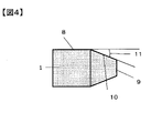
- the end portion of the base material has an R chamfered portion.
- the edge of the base material is R-chamfered, even if the conductive pattern is arranged along the end face shape of the base material, the degree of bending of the conductive pattern is smaller than that in the case where the conductive pattern is not R-chamfered. It is possible to suppress the decrease in conductivity due to the crushing of the material, and it is possible to suppress the increase in the resistance value.
- the shape of the R chamfer and the radius of curvature can be appropriately selected in consideration of the thickness of the base material and the flexibility of the wiring.
- the end portion of the base material has a square chamfered portion having a chamfering angle of 1 ° to 70 ° and a flat portion having a chamfering angle of 0.1 mm or more on the side surface.
- the chamfering angle indicates an angle 11 formed by an extension of the main surface 8 of the base material 1 and a surface 10 having been chamfered.
- the flat portion 9 indicates a portion substantially orthogonal to the main surface 8.
- the chamfering angle is 70 ° or less, an acute-angled portion is unlikely to occur on the side surface portion, and it is possible to suppress a decrease in conductivity due to the collapse of the conductive pattern. Further, by having a flat portion of 0.1 mm or more on the side surface, since the side surface portion does not have an acute-angled portion, it is possible to suppress a decrease in conductivity due to the collapse of the conductive pattern.
- the chamfer angle and width can be appropriately selected in consideration of the thickness and dimensions of the base material and the flexibility of wiring.
- the elastic sheet 4 is opposed to the surface of the film 3 opposite to the pattern forming surface.
- the present invention it is important to use an elastic sheet as the sheet.
- the elastic sheet when the side surface of the base material is pressed against the elastic sheet through the film, the base material sinks into the elastic sheet and the elastic sheet sandwiches the base material. It can be bent and pressurized on both sides and sides of the substrate. Further, even when the pattern is transferred only to the side surface of the base material, the pressure can be uniformly applied, and the crushing of the pattern can be suppressed.
- the sheet is not an elastic body, pressure is not applied to both sides of the base material, and a conductive pattern cannot be formed on the side surface of the base material and the surface of at least one of the substrates.
- the "elastic body” refers to a material having the property of deforming when a load is applied and returning to the original shape when the load is removed.
- the rubber hardness of the elastic sheet measured in accordance with JIS K6253-3: 2012 is preferably 2 to 50.
- the rubber hardness is 2 or more, when the side surface of the base material is pressed against the elastic sheet via the film, the side surface of the substrate is pressurized and a finer pattern can be transferred.
- the rubber hardness is 50 or less, the amount of subduction of the base material is large, the elastic sheet is easily bent, the surface of at least one of the base materials is pressurized, and a finer pattern can be transferred. can.
- the thickness of the elastic sheet is preferably 0.1 to 5.0 mm.
- the thickness of the elastic sheet is 0.1 mm or more, the amount of subduction of the base material is large, the elastic sheet is easily bent, the surface of at least one of the base materials is pressed, and a finer pattern is transferred. can do.
- the thickness is set to 5.0 mm or less, when the heater is used during heating, the heat of the heater can be uniformly transferred to the film having the composition pattern, and the variation in transfer due to temperature unevenness can be suppressed. Can be done.
- the heat resistant temperature of the elastic sheet is preferably 100 ° C. or higher.
- the heat resistant temperature of the elastic sheet is more preferably 140 ° C. or higher.
- the heat resistant temperature is measured according to JIS K6251: 2017, the tensile strength change rate is within ⁇ 30%, the elongation change rate during cutting is within -50%, and is measured according to JIS K6253-3: 2012. It is the maximum temperature value that satisfies all the changes in hardness within ⁇ 15.
- the elastic sheet examples include silicone rubber, urethane rubber, natural rubber, styrene butadiene rubber, chloroprene rubber, butyl rubber, ethylene propylene rubber and the like.
- silicone rubber is preferable because it has high heat resistance and is less likely to undergo thermal shrinkage when pressed against a substrate, and the resulting distortion of the film is suppressed, so that a finer pattern can be transferred.
- the surface in contact with the film is mold-released or uneven.
- the mold release treatment or the uneven processing when the side surface of the base material is pressed against the elastic sheet through the film and separated, the film and the elastic sheet are easily peeled off, and the film is distorted. It is possible to suppress and transfer a finer pattern.
- the release agent used for the release treatment include a long-chain alkyl-based release agent, a silicone-based release agent, and a fluorine-based release agent. Two or more of these may be used.
- the mold release treatment is performed by applying a mold release agent on an elastic sheet and drying it.
- the uneven processing can be performed by a method of casting and molding the elastic resin component on the varnish on the cast support having the unevenness, or a method of heat-pressing the uneven mold onto the surface of the elastic body.
- another elastic sheet may be provided on the surface of the elastic sheet opposite to the surface on which the side surface of the base material is pressed.
- unevenness of pressure at the end of the substrate can be suppressed, and the shape of the pattern can be further suppressed from being crushed.
- by suppressing the shape of the pattern from being crushed it is possible to suppress the decrease in conductivity by sufficiently securing the conductive path of the conductive particles.
- one other sheet is placed on a surface of the elastic sheet 4 (hereinafter, may be referred to as a first elastic sheet) on a surface opposite to the surface on which the side surface of the base material 1 is pressed.
- An embodiment in which an elastic sheet 5 hereinafter, may be referred to as a second elastic sheet
- the other elastic sheet the above-mentioned elastic sheet can be used.
- the rubber hardness of the other elastic sheet measured in accordance with JIS K6253-3: 2012 is preferably 1 to 100.
- the rubber hardness of the other elastic sheet is 1 or more, the restoring force is high, the first elastic sheet is less likely to be distorted before and after unloading, and the crushing of the conductive pattern at the edge of the substrate can be further suppressed. ..
- the rubber hardness of the other elastic sheet is 100 or less, the amount of subduction of the side surface of the base material into the first elastic sheet can be increased, and the force with which the first elastic sheet sandwiches the base material. Is easier to work with, and finer patterns can be transferred.
- the rubber hardness of the other elastic sheet including the second elastic sheet is lower than that of the first elastic sheet, the force for sandwiching the base material of the first elastic sheet is increased, and a finer pattern is obtained. It is preferable from the viewpoint of transferring.
- the thickness of the other elastic sheet is preferably 0.5 mm or more.
- the thickness of the other elastic sheet is 0.5 mm or more, the force for sandwiching the base material of the first elastic sheet becomes easy to work, and a finer pattern can be transferred.
- the side surface of the base material 1 is pressed against the elastic sheet 4 via the film 3, and the pressed portion is heated to obtain the pattern 2. Transfer over the sides and sides of the substrate 1.
- the temperature of the pressing portion is preferably 100 to 200 ° C.
- the "pressing portion” refers to the surface portion of the elastic sheet to which the side surface of the substrate is pressed via the film.
- the temperature of the pressing portion is 100 ° C. or higher, the organic component in the pattern of the composition containing the organic component and the conductive particles formed on the film can be softened and easily transferred to the substrate. , The conductivity of the conductive pattern formed on the base material can be increased.
- the temperature of the pressing portion is 200 ° C. or lower, the heat shrinkage of the film can be suppressed, the disconnection of the pattern due to the film strain can be suppressed, and a finer pattern can be transferred.
- the temperature of the pressing portion can be measured with a non-contact thermometer.
- the time for pressing the side surface of the base material against the elastic sheet is preferably 5 to 300 sec. When the pressing time is 5 sec or more, heat is uniformly transferred to the conductive pattern, and the transferability is further improved. If the pressing time is 300 sec or less, the production tact can be increased. Further, the pressure when the side surface of the base material is pressed against the elastic sheet is preferably 0.1 to 3 MPa or less. When the pressure is 0.1 MPa or more, the adhesion between the conductive pattern of the substrate with the conductive pattern formed and the substrate can be improved. On the other hand, when the pressure is 3 MPa or less, the decrease in conductivity due to the crushing of the pattern at the end of the base material can be further suppressed.
- the side surface of the base material is pressed against the elastic sheet via the film, and both sides of the base material are pressed through the film to press the pressed portion. And it is preferable to transfer the pattern over the side surface of the substrate and the surface of at least one of the substrates by heating the pressurized portion. By doing so, the pressure applied to the side surface of the base material and both sides of the base material can be uniformly controlled, so that the width of the pattern transferred to the side surface of the base material and at least one surface of the substrate can be made uniform.
- the "pressurized portion” refers to the surface portion of the elastic sheet to which at least one surface of the substrate is pressed via the film.
- FIG. 5 shows an embodiment in which the side surface of the base material 1 is pressed against the elastic sheet 4 and both sides of the base material are pressed by a pressure portion.
- the pressurizing method of the pressurizing section is not particularly limited, and examples thereof include a method of applying pressure using a flat plate press, a roll press, or the like.
- the temperature, time, and pressure when pressurizing the pressurizing portion can be the same temperature, time, and pressure as the above-mentioned pressing portion.
- the substrate with a conductive pattern manufactured by the present invention may be additionally heated.
- Examples of the heating method include heating with a drying oven and an infrared oven.
- the heating temperature is preferably 100 to 200 ° C., and the heating time is preferably 5 minutes to 3 hours.
- the substrate with a conductive pattern manufactured by the present invention may be additionally pressed against the elastic sheet on the side surface of the substrate. Further, it may be pressed continuously with the step of transferring the pattern.
- the total time for pressing the side surface of the base material against the elastic sheet is preferably 15 sec to 1800 sec. When the pressing time is 15 sec or more, the conductivity can be increased in a shorter time than the additional heating by the oven. On the other hand, if the pressing time is 1800 sec or less in total, the production tact can be increased.
- a voltage may be additionally applied to the conductive pattern.
- the method of applying the voltage is not particularly limited, and a method of applying a constant voltage using a charge / discharge device, a power source, etc.; a method of applying a pulse voltage; a method of performing a charge / discharge cycle in a constant voltage range, etc. are used. be able to.
- the voltage applied to the conductive pattern is preferably 0.05 to 5.0 V. When the applied voltage is 0.05 V or more, dielectric breakdown occurs in the place where the resin component exists between the conductive particles in the conductive pattern and the conductive path is not formed, the conductive path increases, and the conductivity is improved. Can be high. On the other hand, when the applied voltage is 5.0 V or less, it is possible to suppress the deterioration of the adhesion to the substrate due to the temperature rise in the conductive pattern and the decomposition of the resin component.
- the transfer device of the present invention is a transfer device that transfers a conductive pattern formed on a film over a side surface or a side surface of a base material and at least one surface of the base material, and is the conductive pattern forming surface of the film.
- a support mechanism for holding the elastic sheet arranged on the opposite surface, the side surface of the base material is opposed to the pattern forming surface, and the side surface of the base material is pressed against the elastic sheet via the film. It has a mechanism and a heating mechanism for heating the pressing portion.
- the base material, the film, and the elastic sheet the above-mentioned ones can be used.
- the support mechanism holds the elastic sheet arranged on the surface opposite to the conductive pattern forming surface of the film on which the conductive pattern is formed.
- the elastic sheet is used by being fixed to this support mechanism.
- the support mechanism is preferably a flat SUS plate because heat does not easily escape and distortion of the conductive pattern is unlikely to occur during transfer.
- the pressing mechanism is such that the side surface of the base material is opposed to the pattern forming surface, and the side surface of the base material is pressed against the elastic sheet via the film.
- the pressing mechanism has a portion for fixing the base material.
- a method of fixing the base material a method of adsorbing under reduced pressure by using a jig having suction holes on the surface or a jig made of a porous material, and an adhesive member such as a tape are attached to the part where the base material is fixed. Examples thereof include a method of fixing the base material using a bolt, a method of fixing the base material using a bolt, a method of grasping and fixing a part of the base material, and the like.
- the pressing mechanism has a mechanism for moving a portion for fixing the base material toward the support mechanism.
- the side surface of the base material to be transferred is arranged so as to face the pattern forming surface, and then the portion for fixing the base material is moved toward the support mechanism so that the side surface of the base material becomes the surface. It can be pressed so that it hits from the vertical direction of the pattern surface.
- the heating mechanism is a mechanism for heating the above-mentioned pressing portion, and heats from the surface of the support mechanism opposite to the surface on which the elastic sheet is fixed.
- the heating method can be heated by using a heater or the like.
- Specific resistance resistance value x film thickness x line width / line length ... (1).
- the obtained 16.0 g of the resin solution 1 and 25.7 g of the Ag powder were mixed and kneaded using a three-roller mill (EXAKT M-50; manufactured by EXAKT), and the ratio of the conductive particles in the solid content was increased. 70% by weight of the conductive paste 1 was obtained.
- Example 1 The conductive paste 1 was applied to the release surface of the release film AL-5 by screen printing so as to have the pattern shape shown in FIG. 6 so that the film thickness after drying was 4.0 ⁇ m, and the obtained coating film was 100. It was dried in a drying oven at ° C. for 10 minutes to form a pattern. The side surface of the glass substrate was opposed to the formed pattern forming surface, and the elastic sheet A installed on the hot plate was opposed to the surface opposite to the pattern forming surface of the film as shown in FIG.
- the side surface of the glass substrate is pressed against the elastic sheet A via a film under the conditions of 210 ° C., 60 sec, and 0.35 MPa to obtain a substrate with a wiring pattern, and then heated in a drying oven at 140 ° C. for 1 hour.
- a substrate with a conductive pattern was obtained.
- the evaluation results are shown in Table 4.
- the temperature of the pressing portion was adjusted to the condition temperature by using an infrared radiation thermometer (manufactured by A & D, product name AD-5635).
- Example 2 Conductive paste 2 was applied to the release surface of the release film AL-5 by screen printing so that the film thickness after drying was 4.0 ⁇ m.
- the obtained coating film is dried in a drying oven at 100 ° C. for 10 minutes, and exposed to 350 mJ / cm 2 using an exposure machine equipped with an ultra-high pressure mercury lamp via a photomask through which the pattern portion of FIG. 6 is transparent. Exposed in quantity.
- a 0.1 mass% sodium carbonate aqueous solution was used as a developer and spray-developed at a pressure of 0.1 MPa for 30 seconds to form a pattern.
- the side surface of the glass substrate was opposed to the formed pattern forming surface, and the elastic sheet A installed on the hot plate was opposed to the surface opposite to the pattern forming surface of the film as shown in FIG.
- the side surface of the glass substrate is pressed against the elastic sheet A via a film under the conditions of 170 ° C., 60 sec, and 0.35 MPa to obtain a substrate with a wiring pattern, and then heated in a drying oven at 140 ° C. for 1 hour to obtain a conductive pattern. I got a board with.
- the evaluation results are shown in Table 4.
- Examples 3 to 8 A substrate with a conductive pattern was obtained in the same manner as in Example 2 except that the type of elastic sheet and the transfer conditions were changed as shown in Table 1. The evaluation results are shown in Table 4.
- Example 9 Conductive paste 2 was applied to the release surface of the release film AL-5 by screen printing so that the film thickness after drying was 4.0 ⁇ m.
- the obtained coating film is dried in a drying oven at 100 ° C. for 10 minutes, and exposed to 350 mJ / cm 2 using an exposure machine equipped with an ultra-high pressure mercury lamp via a photomask through which the pattern portion of FIG. 6 is transparent. Exposed in quantity.
- a 0.1 mass% sodium carbonate aqueous solution was used as a developer and spray-developed at a pressure of 0.1 MPa for 30 seconds to form a pattern.
- the side surface of the glass substrate was opposed to the formed pattern forming surface, and the elastic sheet E installed on the hot plate was opposed to the surface opposite to the pattern forming surface of the film as shown in FIG.
- the side surface of the glass substrate is pressed against the elastic sheet E via the film under the conditions of 170 ° C., 60 sec, and 0.35 MPa, and both sides of the glass substrate are pressed under the same conditions via the film using a small heated flat plate press. After pressurizing to obtain a substrate with a wiring pattern, the substrate was heated at 140 ° C. for 1 hour in a drying oven to obtain a substrate with a conductive pattern.
- Table 4 The evaluation results are shown in Table 4.
- Conductive paste 2 was applied to the release surface of the release film AL-5 by screen printing so that the film thickness after drying was 4.0 ⁇ m.
- the obtained coating film is dried in a drying oven at 100 ° C. for 10 minutes, and exposed to 350 mJ / cm 2 using an exposure machine equipped with an ultra-high pressure mercury lamp via a photomask through which the pattern portion of FIG. 6 is transparent. Exposed in quantity.
- a 0.1 mass% sodium carbonate aqueous solution was used as a developer and spray-developed at a pressure of 0.1 MPa for 30 seconds to form a pattern.
- the side surface of the glass substrate was opposed to the formed pattern-forming surface and pressed against a hot plate at 170 ° C.
- Example 10 Conductive paste 2 was applied to the release surface of the release film AL-5 by screen printing so that the film thickness after drying was 4.0 ⁇ m.
- the obtained coating film is dried in a drying oven at 100 ° C. for 10 minutes, and exposed to 350 mJ / cm 2 using an exposure machine equipped with an ultra-high pressure mercury lamp via a photomask through which the pattern portion of FIG. 6 is transparent. Exposed in quantity.
- a 0.1 mass% sodium carbonate aqueous solution was used as a developer and spray-developed at a pressure of 0.1 MPa for 30 seconds to form a pattern.
- the elastic sheet E is used as the first elastic sheet and another elastic sheet is used as the second elastic sheet from the side closer to the glass substrate as shown in FIG.
- the elastic sheet laminates in which two elastic sheets are laminated are opposed to each other, and the side surfaces of the glass substrate are placed on the elastic sheet laminates via a film at 170 ° C., 60 sec, 0.35 MPa.
- a substrate with a wiring pattern was obtained by pressing under the conditions. Then, the substrate was heated at 140 ° C. for 1 hour in a drying oven to obtain a substrate with a conductive pattern.
- Table 4 The evaluation results are shown in Table 4.
- Example 11 Conductive paste 2 was applied to the release surface of the release film AL-5 by screen printing so that the film thickness after drying was 4.0 ⁇ m.
- the obtained coating film is dried in a drying oven at 100 ° C. for 10 minutes, and exposed to 350 mJ / cm 2 using an exposure machine equipped with an ultra-high pressure mercury lamp via a photomask through which the pattern portion of FIG. 6 is transparent. Exposed in quantity.
- a 0.1 mass% sodium carbonate aqueous solution was used as a developer and spray-developed at a pressure of 0.1 MPa for 30 seconds to form a pattern.
- the elastic sheet E is used as the first elastic sheet and another elastic sheet is used as the second elastic sheet from the side closer to the glass substrate as shown in FIG.
- the elastic sheet laminate in which the two elastic sheets are laminated is opposed to each other, and the side surface and both sides of the glass substrate are placed on the elastic sheet laminate via a film at 170 ° C., 60 sec, 0.
- a substrate with a wiring pattern was obtained by pressing under the condition of 35 MPa and pressing both sides of the glass substrate through a film under the same conditions using a heating type small flat plate press. Then, the substrate was heated at 140 ° C. for 1 hour in a drying oven to obtain a substrate with a conductive pattern.
- the evaluation results are shown in Table 4.
- Example 12 As shown in Table 2, an elastic sheet laminated body in which two elastic body sheets are laminated in the order of elastic body sheet E as the first elastic body sheet and elastic body sheet F as the second elastic body sheet was used. A substrate with a conductive pattern was obtained in the same manner as in Example 10 except for the above. The evaluation results are shown in Table 4.
- Example 13 As shown in Table 2, a substrate with a conductive pattern was obtained in the same manner as in Example 12 except that the temperature when the side surface of the glass substrate was pressed against the elastic sheet laminate via the film was set to 150 ° C. The evaluation results are shown in Table 4.
- Example 14 Conductive paste 2 was applied to the release surface of the release film AL-5 by screen printing so that the film thickness after drying was 4.0 ⁇ m.
- the obtained coating film is dried in a drying oven at 100 ° C. for 10 minutes, and exposed to 350 mJ / cm 2 using an exposure machine equipped with an ultra-high pressure mercury lamp via a photomask through which the pattern portion of FIG. 6 is transparent. Exposed in quantity.
- a 0.1 mass% sodium carbonate aqueous solution was used as a developer and spray-developed at a pressure of 0.1 MPa for 30 seconds to form a pattern.
- Example 15 to 17 A substrate with a conductive pattern was obtained in the same manner as in Example 14 except that the transfer conditions were changed as shown in Table 2. The evaluation results are shown in Table 4.
- Example 18 Conductive paste 2 was applied to the release surface of the release film AL-5 by screen printing so that the film thickness after drying was 4.0 ⁇ m.
- the obtained coating film is dried in a drying oven at 100 ° C. for 10 minutes, and exposed to 350 mJ / cm 2 using an exposure machine equipped with an ultra-high pressure mercury lamp via a photomask through which the pattern portion of FIG. 6 is transparent. Exposed in quantity.
- a 0.1 mass% sodium carbonate aqueous solution was used as a developer and spray-developed at a pressure of 0.1 MPa for 30 seconds to form a pattern.
- two elastic body sorts are laminated in the order of the elastic body sheet E as the first elastic body sheet and the elastic body sheet F as the second elastic body sheet.
- the elastic sheet laminates were opposed to each other, and the side surfaces of the glass substrate were pressed against the elastic laminates at 170 ° C., 60 sec, and 0.35 MPa under the conditions of 170 ° C., 60 sec, and 0.35 MPa to obtain a substrate with a conductive pattern, and then a drying oven.
- the substrate was heated at 140 ° C. for 1 hour to obtain a substrate with a conductive pattern.
- Substrate 2 Pattern 3: Film 4: Elastic sheet 5: Other elastic sheet 6: Electrode on the front surface of the substrate 7: Electrode on the back surface of the substrate 8: Main surface 9 of the substrate 9: Flat portion on the side surface 10 : Square chamfered surface 11: Chamfering angle 12: Conductive pattern 13: Release film 14: Glass substrate
Landscapes
- Engineering & Computer Science (AREA)
- Manufacturing & Machinery (AREA)
- Microelectronics & Electronic Packaging (AREA)
- Manufacturing Of Printed Wiring (AREA)
Priority Applications (1)
| Application Number | Priority Date | Filing Date | Title |
|---|---|---|---|
| JP2021559011A JPWO2022102245A1 (https=) | 2020-11-10 | 2021-09-17 |
Applications Claiming Priority (6)
| Application Number | Priority Date | Filing Date | Title |
|---|---|---|---|
| JP2020-187044 | 2020-11-10 | ||
| JP2020187044 | 2020-11-10 | ||
| JP2021-052856 | 2021-03-26 | ||
| JP2021052856 | 2021-03-26 | ||
| JP2021108521 | 2021-06-30 | ||
| JP2021-108521 | 2021-06-30 |
Publications (1)
| Publication Number | Publication Date |
|---|---|
| WO2022102245A1 true WO2022102245A1 (ja) | 2022-05-19 |
Family
ID=81601913
Family Applications (1)
| Application Number | Title | Priority Date | Filing Date |
|---|---|---|---|
| PCT/JP2021/034304 Ceased WO2022102245A1 (ja) | 2020-11-10 | 2021-09-17 | 導電パターン付き基板の製造方法および転写装置 |
Country Status (3)
| Country | Link |
|---|---|
| JP (1) | JPWO2022102245A1 (https=) |
| TW (1) | TW202220512A (https=) |
| WO (1) | WO2022102245A1 (https=) |
Citations (4)
| Publication number | Priority date | Publication date | Assignee | Title |
|---|---|---|---|---|
| JPS59149086A (ja) * | 1983-02-15 | 1984-08-25 | 松下電器産業株式会社 | 曲面印刷装置 |
| JPS61253889A (ja) * | 1985-05-07 | 1986-11-11 | 株式会社日本製鋼所 | 電子部品用基板への転写配線方法及び装置 |
| JPH0521302A (ja) * | 1991-07-15 | 1993-01-29 | Murata Mfg Co Ltd | 基板側面の電極形成方法及びその装置 |
| JP2018120652A (ja) * | 2017-01-23 | 2018-08-02 | 東レ株式会社 | 導電パターン形成用フィルム |
-
2021
- 2021-09-17 JP JP2021559011A patent/JPWO2022102245A1/ja active Pending
- 2021-09-17 WO PCT/JP2021/034304 patent/WO2022102245A1/ja not_active Ceased
- 2021-10-08 TW TW110137476A patent/TW202220512A/zh unknown
Patent Citations (4)
| Publication number | Priority date | Publication date | Assignee | Title |
|---|---|---|---|---|
| JPS59149086A (ja) * | 1983-02-15 | 1984-08-25 | 松下電器産業株式会社 | 曲面印刷装置 |
| JPS61253889A (ja) * | 1985-05-07 | 1986-11-11 | 株式会社日本製鋼所 | 電子部品用基板への転写配線方法及び装置 |
| JPH0521302A (ja) * | 1991-07-15 | 1993-01-29 | Murata Mfg Co Ltd | 基板側面の電極形成方法及びその装置 |
| JP2018120652A (ja) * | 2017-01-23 | 2018-08-02 | 東レ株式会社 | 導電パターン形成用フィルム |
Also Published As
| Publication number | Publication date |
|---|---|
| TW202220512A (zh) | 2022-05-16 |
| JPWO2022102245A1 (https=) | 2022-05-19 |
Similar Documents
| Publication | Publication Date | Title |
|---|---|---|
| JP6750685B2 (ja) | 感光性導電ペーストおよび導電パターン形成用フィルム | |
| WO2019202889A1 (ja) | 感光性導電ペーストおよびそれを用いたパターン形成グリーンシートの製造方法 | |
| TWI326394B (https=) | ||
| JP4781158B2 (ja) | 保護膜形成用ドライフィルムおよびそれを用いた加工品 | |
| TWI641000B (zh) | 接觸感測器用積層圖案的製造方法、接觸感測器及觸控面板 | |
| WO2022102245A1 (ja) | 導電パターン付き基板の製造方法および転写装置 | |
| TWI658382B (zh) | 觸摸感測器用構件的製造方法及觸摸感測器用構件 | |
| KR102722567B1 (ko) | 도전 페이스트, 프린트 배선판, 프린트 배선판의 제조방법, 프린트 회로판의 제조방법 | |
| WO2017208842A1 (ja) | 積層パターン形成基材及びタッチパネルの製造方法 | |
| CN108292540A (zh) | 电极层支承用绝缘糊剂、触控面板、触控面板的制造方法 | |
| JP6717439B1 (ja) | 積層部材 | |
| JP2022062573A (ja) | 感光性積層樹脂構造体、ドライフィルム、硬化物および電子部品 | |
| JP2022151702A (ja) | 回路基板、積層回路基板およびウェアラブルデバイス | |
| TW202501156A (zh) | 感光性導電組成物、使用其之積層體、感光性導電接著劑、附圖案之基板之製造方法及顯示器基板 | |
| KR20210120991A (ko) | 배선 기판 및 그 제조 방법, 및 고전도 배선 기판의 제조 방법 | |
| JP2003243805A (ja) | 回路形成用転写材及び回路基板の製造方法 | |
| JP2025165434A (ja) | 電子部品の製造方法および樹脂組成物 | |
| WO2026088714A1 (ja) | 感光性導電ペースト、それを用いた硬化物、焼成体および電子部品 | |
| CN119138109A (zh) | 带凸块的结构物的制造方法及具有凸块图案的基板 | |
| JP2021152988A (ja) | 導電ペースト、導電パターン形成用フィルム、積層部材及びタッチパネル | |
| JP2001133992A (ja) | パターン形成材料付き積層フィルムおよびその積層フィルムを用いるパターン転写方法 |
Legal Events
| Date | Code | Title | Description |
|---|---|---|---|
| ENP | Entry into the national phase |
Ref document number: 2021559011 Country of ref document: JP Kind code of ref document: A |
|
| 121 | Ep: the epo has been informed by wipo that ep was designated in this application |
Ref document number: 21891493 Country of ref document: EP Kind code of ref document: A1 |
|
| NENP | Non-entry into the national phase |
Ref country code: DE |
|
| 122 | Ep: pct application non-entry in european phase |
Ref document number: 21891493 Country of ref document: EP Kind code of ref document: A1 |