WO2022085555A1 - 光電変換装置、光電変換システム - Google Patents
光電変換装置、光電変換システム Download PDFInfo
- Publication number
- WO2022085555A1 WO2022085555A1 PCT/JP2021/038032 JP2021038032W WO2022085555A1 WO 2022085555 A1 WO2022085555 A1 WO 2022085555A1 JP 2021038032 W JP2021038032 W JP 2021038032W WO 2022085555 A1 WO2022085555 A1 WO 2022085555A1
- Authority
- WO
- WIPO (PCT)
- Prior art keywords
- exposure period
- photoelectric conversion
- period
- conversion device
- exposure
- Prior art date
- Legal status (The legal status is an assumption and is not a legal conclusion. Google has not performed a legal analysis and makes no representation as to the accuracy of the status listed.)
- Ceased
Links
Images


Classifications
-
- H—ELECTRICITY
- H04—ELECTRIC COMMUNICATION TECHNIQUE
- H04N—PICTORIAL COMMUNICATION, e.g. TELEVISION
- H04N25/00—Circuitry of solid-state image sensors [SSIS]; Control thereof
- H04N25/70—SSIS architectures; Circuits associated therewith
- H04N25/76—Addressed sensors, e.g. MOS or CMOS sensors
- H04N25/77—Pixel circuitry, e.g. memories, A/D converters, pixel amplifiers, shared circuits or shared components
- H04N25/772—Pixel circuitry, e.g. memories, A/D converters, pixel amplifiers, shared circuits or shared components comprising A/D, V/T, V/F, I/T or I/F converters
- H04N25/773—Pixel circuitry, e.g. memories, A/D converters, pixel amplifiers, shared circuits or shared components comprising A/D, V/T, V/F, I/T or I/F converters comprising photon counting circuits, e.g. single photon detection [SPD] or single photon avalanche diodes [SPAD]
-
- G—PHYSICS
- G01—MEASURING; TESTING
- G01S—RADIO DIRECTION-FINDING; RADIO NAVIGATION; DETERMINING DISTANCE OR VELOCITY BY USE OF RADIO WAVES; LOCATING OR PRESENCE-DETECTING BY USE OF THE REFLECTION OR RERADIATION OF RADIO WAVES; ANALOGOUS ARRANGEMENTS USING OTHER WAVES
- G01S17/00—Systems using the reflection or reradiation of electromagnetic waves other than radio waves, e.g. lidar systems
- G01S17/02—Systems using the reflection of electromagnetic waves other than radio waves
- G01S17/06—Systems determining position data of a target
- G01S17/08—Systems determining position data of a target for measuring distance only
- G01S17/10—Systems determining position data of a target for measuring distance only using transmission of interrupted, pulse-modulated waves
-
- G—PHYSICS
- G01—MEASURING; TESTING
- G01S—RADIO DIRECTION-FINDING; RADIO NAVIGATION; DETERMINING DISTANCE OR VELOCITY BY USE OF RADIO WAVES; LOCATING OR PRESENCE-DETECTING BY USE OF THE REFLECTION OR RERADIATION OF RADIO WAVES; ANALOGOUS ARRANGEMENTS USING OTHER WAVES
- G01S17/00—Systems using the reflection or reradiation of electromagnetic waves other than radio waves, e.g. lidar systems
- G01S17/88—Lidar systems specially adapted for specific applications
- G01S17/89—Lidar systems specially adapted for specific applications for mapping or imaging
- G01S17/894—3D imaging with simultaneous measurement of time-of-flight at a 2D array of receiver pixels, e.g. time-of-flight cameras or flash lidar
-
- G—PHYSICS
- G01—MEASURING; TESTING
- G01S—RADIO DIRECTION-FINDING; RADIO NAVIGATION; DETERMINING DISTANCE OR VELOCITY BY USE OF RADIO WAVES; LOCATING OR PRESENCE-DETECTING BY USE OF THE REFLECTION OR RERADIATION OF RADIO WAVES; ANALOGOUS ARRANGEMENTS USING OTHER WAVES
- G01S17/00—Systems using the reflection or reradiation of electromagnetic waves other than radio waves, e.g. lidar systems
- G01S17/88—Lidar systems specially adapted for specific applications
- G01S17/93—Lidar systems specially adapted for specific applications for anti-collision purposes
- G01S17/931—Lidar systems specially adapted for specific applications for anti-collision purposes of land vehicles
-
- G—PHYSICS
- G01—MEASURING; TESTING
- G01S—RADIO DIRECTION-FINDING; RADIO NAVIGATION; DETERMINING DISTANCE OR VELOCITY BY USE OF RADIO WAVES; LOCATING OR PRESENCE-DETECTING BY USE OF THE REFLECTION OR RERADIATION OF RADIO WAVES; ANALOGOUS ARRANGEMENTS USING OTHER WAVES
- G01S7/00—Details of systems according to groups G01S13/00, G01S15/00, G01S17/00
- G01S7/48—Details of systems according to groups G01S13/00, G01S15/00, G01S17/00 of systems according to group G01S17/00
- G01S7/481—Constructional features, e.g. arrangements of optical elements
- G01S7/4816—Constructional features, e.g. arrangements of optical elements of receivers alone
-
- G—PHYSICS
- G01—MEASURING; TESTING
- G01S—RADIO DIRECTION-FINDING; RADIO NAVIGATION; DETERMINING DISTANCE OR VELOCITY BY USE OF RADIO WAVES; LOCATING OR PRESENCE-DETECTING BY USE OF THE REFLECTION OR RERADIATION OF RADIO WAVES; ANALOGOUS ARRANGEMENTS USING OTHER WAVES
- G01S7/00—Details of systems according to groups G01S13/00, G01S15/00, G01S17/00
- G01S7/48—Details of systems according to groups G01S13/00, G01S15/00, G01S17/00 of systems according to group G01S17/00
- G01S7/483—Details of pulse systems
- G01S7/486—Receivers
- G01S7/4861—Circuits for detection, sampling, integration or read-out
- G01S7/4863—Detector arrays, e.g. charge-transfer gates
-
- G—PHYSICS
- G01—MEASURING; TESTING
- G01S—RADIO DIRECTION-FINDING; RADIO NAVIGATION; DETERMINING DISTANCE OR VELOCITY BY USE OF RADIO WAVES; LOCATING OR PRESENCE-DETECTING BY USE OF THE REFLECTION OR RERADIATION OF RADIO WAVES; ANALOGOUS ARRANGEMENTS USING OTHER WAVES
- G01S7/00—Details of systems according to groups G01S13/00, G01S15/00, G01S17/00
- G01S7/48—Details of systems according to groups G01S13/00, G01S15/00, G01S17/00 of systems according to group G01S17/00
- G01S7/483—Details of pulse systems
- G01S7/486—Receivers
- G01S7/4865—Time delay measurement, e.g. time-of-flight measurement, time of arrival measurement or determining the exact position of a peak
-
- G—PHYSICS
- G01—MEASURING; TESTING
- G01S—RADIO DIRECTION-FINDING; RADIO NAVIGATION; DETERMINING DISTANCE OR VELOCITY BY USE OF RADIO WAVES; LOCATING OR PRESENCE-DETECTING BY USE OF THE REFLECTION OR RERADIATION OF RADIO WAVES; ANALOGOUS ARRANGEMENTS USING OTHER WAVES
- G01S7/00—Details of systems according to groups G01S13/00, G01S15/00, G01S17/00
- G01S7/48—Details of systems according to groups G01S13/00, G01S15/00, G01S17/00 of systems according to group G01S17/00
- G01S7/491—Details of non-pulse systems
- G01S7/4912—Receivers
- G01S7/4913—Circuits for detection, sampling, integration or read-out
-
- H—ELECTRICITY
- H04—ELECTRIC COMMUNICATION TECHNIQUE
- H04N—PICTORIAL COMMUNICATION, e.g. TELEVISION
- H04N25/00—Circuitry of solid-state image sensors [SSIS]; Control thereof
- H04N25/50—Control of the SSIS exposure
- H04N25/53—Control of the integration time
-
- H—ELECTRICITY
- H04—ELECTRIC COMMUNICATION TECHNIQUE
- H04N—PICTORIAL COMMUNICATION, e.g. TELEVISION
- H04N25/00—Circuitry of solid-state image sensors [SSIS]; Control thereof
- H04N25/70—SSIS architectures; Circuits associated therewith
- H04N25/76—Addressed sensors, e.g. MOS or CMOS sensors
- H04N25/77—Pixel circuitry, e.g. memories, A/D converters, pixel amplifiers, shared circuits or shared components
- H04N25/771—Pixel circuitry, e.g. memories, A/D converters, pixel amplifiers, shared circuits or shared components comprising storage means other than floating diffusion
-
- H—ELECTRICITY
- H04—ELECTRIC COMMUNICATION TECHNIQUE
- H04N—PICTORIAL COMMUNICATION, e.g. TELEVISION
- H04N25/00—Circuitry of solid-state image sensors [SSIS]; Control thereof
- H04N25/70—SSIS architectures; Circuits associated therewith
- H04N25/79—Arrangements of circuitry being divided between different or multiple substrates, chips or circuit boards, e.g. stacked image sensors
-
- H—ELECTRICITY
- H10—SEMICONDUCTOR DEVICES; ELECTRIC SOLID-STATE DEVICES NOT OTHERWISE PROVIDED FOR
- H10F—INORGANIC SEMICONDUCTOR DEVICES SENSITIVE TO INFRARED RADIATION, LIGHT, ELECTROMAGNETIC RADIATION OF SHORTER WAVELENGTH OR CORPUSCULAR RADIATION
- H10F30/00—Individual radiation-sensitive semiconductor devices in which radiation controls the flow of current through the devices, e.g. photodetectors
- H10F30/20—Individual radiation-sensitive semiconductor devices in which radiation controls the flow of current through the devices, e.g. photodetectors the devices having potential barriers, e.g. phototransistors
- H10F30/21—Individual radiation-sensitive semiconductor devices in which radiation controls the flow of current through the devices, e.g. photodetectors the devices having potential barriers, e.g. phototransistors the devices being sensitive to infrared, visible or ultraviolet radiation
- H10F30/22—Individual radiation-sensitive semiconductor devices in which radiation controls the flow of current through the devices, e.g. photodetectors the devices having potential barriers, e.g. phototransistors the devices being sensitive to infrared, visible or ultraviolet radiation the devices having only one potential barrier, e.g. photodiodes
- H10F30/225—Individual radiation-sensitive semiconductor devices in which radiation controls the flow of current through the devices, e.g. photodetectors the devices having potential barriers, e.g. phototransistors the devices being sensitive to infrared, visible or ultraviolet radiation the devices having only one potential barrier, e.g. photodiodes the potential barrier working in avalanche mode, e.g. avalanche photodiodes
-
- H—ELECTRICITY
- H10—SEMICONDUCTOR DEVICES; ELECTRIC SOLID-STATE DEVICES NOT OTHERWISE PROVIDED FOR
- H10F—INORGANIC SEMICONDUCTOR DEVICES SENSITIVE TO INFRARED RADIATION, LIGHT, ELECTROMAGNETIC RADIATION OF SHORTER WAVELENGTH OR CORPUSCULAR RADIATION
- H10F77/00—Constructional details of devices covered by this subclass
- H10F77/95—Circuit arrangements
- H10F77/953—Circuit arrangements for devices having potential barriers
- H10F77/959—Circuit arrangements for devices having potential barriers for devices working in avalanche mode
Definitions
- the present invention relates to a photoelectric conversion device and a photoelectric conversion system.
- the TOF Time Of Flight
- this TOF method light is emitted from a light source and the reflected light reflected by the object to be measured is detected. Then, in the TOF method, the distance to the object to be measured is measured by measuring the time difference between the timing at which the light is emitted and the timing at which the reflected light is detected.
- Patent Document 1 discloses a TOF ranging device using a SPAD (Single Photon Avalanche Diode) in which a light charge caused by a single photon causes an avalanche multiplication in a PN junction region of a semiconductor region constituting a photoelectric conversion unit. ing. Further, in Patent Document 1, a state in which a photon signal incident on a SPAD is detected (exposed state) and a state in which it is not detected (non-exposed state) are switched at high speed by a pulse signal having a range on the order of picoseconds to microseconds. Distance measurement by the time gate method is described.
- SPAD Single Photon Avalanche Diode
- Patent Document 1 in order to accurately measure the time distribution of the detected light, it is necessary to scan the relative difference between the light emission timing and the time gate timing at fine intervals within the time range corresponding to the predetermined distance measurement range. There is. Therefore, the time required for one distance measurement increases, and it is difficult to speed up the distance measurement from the photoelectric conversion device to the object to be measured.
- the photoelectric conversion device is based on the signal charge generated in the photoelectric conversion unit and the second exposure period in which at least one of the start timing and the end timing is different from the first exposure period and the first exposure period.
- a light amount value holding unit that holds the light amount value
- a comparison unit that compares the light amount value based on the signal charge generated in the first exposure period, and the light amount value based on the signal charge generated in the second exposure period, and a comparison unit.
- a control unit controls to set a fourth exposure period in which at least one of the start timing and the end timing is different between the third exposure period and the third exposure period.
- the third exposure period and the fourth exposure period are shorter than at least one of the first exposure period and the second exposure period.
- the photoelectric conversion device is obtained by incident on the photoelectric conversion unit in a second exposure period in which at least one of the start timing and the end timing is different from the first exposure period and the first exposure period. It has a light amount value holding unit that holds a light amount value based on a signal charge, and a comparison unit that compares the light amount value obtained in the first exposure period with the light amount value obtained in the second exposure period. A control unit that controls a third exposure period and a fourth exposure period according to the comparison result of the comparison unit.
- the measurement of the distance from the photoelectric conversion device to the object to be measured can be speeded up as compared with Patent Document 1.
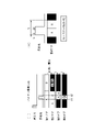
- FIG. 1 is a block diagram of the photoelectric conversion device 100 of the present embodiment.
- the photoelectric conversion device 100 includes a pixel unit 101, a control pulse generation unit 115, a horizontal scanning circuit unit 111, a readout circuit 112, a signal line 113, and a vertical scanning circuit unit 110.
- a plurality of pixels 104 are arranged in a two-dimensional array (matrix) in the pixel unit 101.
- One pixel 104 is composed of a photoelectric conversion unit 102 including an avalanche photodiode (hereinafter referred to as APD) and a pixel circuit 103.
- APD avalanche photodiode
- the photoelectric conversion unit 102 converts light into an electric signal.
- the pixel circuit 103 outputs the electric signal converted by the photoelectric conversion unit 102 to the signal line 113.
- the vertical scanning circuit unit 110 receives the control pulse supplied from the control pulse generation unit 115 and supplies the control pulse to each pixel.
- a logic circuit such as a shift register or an address decoder is used in the vertical scanning circuit unit 110.
- the signal output from the photoelectric conversion unit 102 of each pixel is processed by the pixel circuit 103.
- the pixel circuit 103 is provided with a counter circuit and / or a memory.
- a case where the pixel circuit 103 has a memory will be described. Digital values are stored in memory.
- the horizontal scanning circuit unit 111 inputs a control pulse for sequentially selecting each column to the pixel circuit 103 in order to read a signal from the memory of each pixel in which the digital signal is held.
- the signal from the pixel circuit 103 of the pixel 104 selected by the vertical scanning circuit unit 110 is output to the signal line 113 for the selected line.
- the signal output to the signal line 113 is output to an external recording unit or signal processing unit of the photoelectric conversion device 100 via the output circuit 114.
- pixels 104 are arranged in a two-dimensional array in the pixel unit 101.
- a plurality of pixels 104 may be arranged one-dimensionally in the pixel unit 101.
- the pixel unit 101 may be arranged with only a single pixel instead of an array.
- the function of the pixel circuit 103 does not necessarily have to be provided for every pixel 104 one by one.
- one pixel circuit 103 may be shared by a plurality of pixels 104, and signal processing may be sequentially performed.
- the photoelectric conversion device a laminated sensor in which a first substrate having a photoelectric conversion unit and a second substrate having a pixel circuit are laminated and bonded may be used in order to increase the sensitivity and functionality. In this case, the photoelectric conversion unit and the pixel circuit are electrically connected via the connection wiring provided for each pixel.
- FIG. 2 (i) is a diagram showing a comparative form, and is an explanatory diagram of a method of linearly searching the timing of reflected light among the time gate type TOF methods.
- FIG. 2 (ii) is an explanatory diagram of a method of performing a binary search for the timing of reflected light according to the present embodiment.
- the range shown in white in each subframe is the exposure period of the pixel 104, and the range shown in black is the non-exposure period.
- the exposure period refers to, for example, a period in which the photoelectric conversion unit 102 is active and the signal from the photoelectric conversion unit 102 is read out to the counter circuit and / or the register circuit.
- the non-exposure period refers to a period during which the signal from the photoelectric conversion unit 102 is not read out in the counter circuit and / or the register circuit.
- the APD is exposed to a period in which a reverse bias potential capable of multiplying the avalanche is applied, the gate element is turned on, and the signal from the APD can be read out by the counter circuit and / register circuit. It is a period. Then, the period in which the gate element is turned off and the signal from the APD is not read through the gate element is defined as the non-exposure period.
- the non-exposure period is not limited to this.
- the non-exposure period may be a period for reducing the potential difference applied to the APD so that the avalanche multiplication does not occur in the APD
- the exposure period may be the period for applying the potential difference such that the APD increases the avalanche.
- the period for controlling the counter circuit and / or the register circuit so as not to be driven may be the non-exposure period
- the period for controlling the counter circuit and / or the register circuit to be driven may be the exposure period.
- subframes are arranged from the emitted light for the sake of clarity, but in actual driving, the first emitted light is the first subframe. The amount of light is measured. After that, the second emitted light is emitted at the same timing as the first emitted light, and the light amount of the second subframe is measured by the second emitted light. Then, the light amount of the Nth subframe is measured by the Nth emission light.
- the amount of light is measured N times while shifting the relative timing between the start timing and the end timing of the exposure period with respect to the light emission timing of the light source. That is, the reflected light is measured while gradually shifting the start timing of the exposure period.
- the timing of the exposure period is linearly scanned in steps with respect to a predetermined ranging range
- the time resolution or ranging accuracy of the reflected light detection is higher in proportion to the number of steps N of the linear scanning. Become. However, as the number of steps increases and the number of subframes increases, it takes time to measure the distance.
- the period corresponding to the period of the emitted light is time-divisioned into two or more exposure periods.
- the exposure periods A and B are time-divided, the light intensity in each exposure period is independently measured, and the magnitude of the light intensity in the exposure periods A and B is compared.
- the amount of optical signals in the exposure period A is larger than the amount of optical signals in the exposure period B. Based on this comparison result, it is assumed that the reflected light is included in the exposure period A, and the exposure period A is further divided into two within the range of the length of the exposure period A of the first subframe.
- the linear search requires N times of light amount measurement, whereas the binary search can suppress the number of light amount measurements to Log2 (N), so that the distance measurement can be speeded up.
- each subframe is shown only for one light irradiation and one exposure period in FIG. 2 (i)
- an optical signal obtained by repeating each subframe a plurality of times may be added. This makes it possible to improve the accuracy of optical signal measurement.
- the time resolution or distance measurement accuracy of the reflected light detection increases in proportion to the number of steps N of the linear scanning.
- FIG. 2 (ii) shows an example of dividing the exposure period into two equal parts as a binary search method.
- the term binary search method is not limited to the one in which the exposure period is halved, and the exposure period is set to three or more halves.
- the search method is also referred to as a binary search method in this specification. That is, the binary search method is a name different from the linear scanning method, and is not limited to two equal parts. Further, the lengths of the two exposure periods A and B in one subframe may be different. Further, in the step of comparison, the signals A'and B'that have been subjected to predetermined arithmetic processing or correction processing to the respective signals may be compared instead of the signal amounts themselves of the exposure periods A and B.
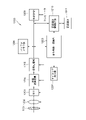
- FIG. 3 is an example of a block diagram per unit pixel in this embodiment.
- the pixel has a photoelectric conversion unit and a pixel circuit.
- APD301 is used as the photoelectric conversion unit.
- the pixel circuit includes a quench element 302, a gate element 303 (switch), a light amount value holding unit 31, a comparison circuit (comparison unit) 312, a register circuit 313, and a pulse generation circuit 314.
- the light quantity value holding unit 31 has a counter circuit 310 and a register circuit 311.
- the APD 301 is connected to the quench element 302 that controls the avalanche current.
- the photon detection signal output from the APD 301 is temporally controlled by the gate signal GATE input to the gate element 303.
- the output of the gate element 303 is input to the light quantity value holding unit 31 including the counter circuit 310 and the register circuit 311.
- the photon signal that has passed through the gate element 303 is counted by the counter circuit 310, and the count value is written to the register circuit 311 according to the trigger signal RTRG. That is, the register circuit 311 functions as a recording circuit.
- the comparison circuit 312 receives the enable signal COEN, compares the magnitude of the output values of the counter circuit 310 and the register circuit 311 and records the comparison result in the register circuit 313.
- the pulse generation circuit 314 receives the holding signal of the register circuit 313, the clock signal CLK, and the enable signal PGEN, and generates a gate signal GATE that defines the exposure pattern.
- the reset signals RES1, RES2, and RES3 initialize the holding signals of the counter circuit 310, the register circuit 311 and the register circuit 313, respectively.
- APD301 generates a charge pair according to the incident light by photoelectric conversion.
- a potential based on the potential VH higher than the potential VL supplied to the anode is supplied to the cathode of the APD 301.
- a potential is supplied to the anode and cathode of the APD 301 so that a reverse bias is applied so that the photons incident on the APD 301 are multiplied by the avalanche.
- the electric charge generated by the incident light causes an avalanche multiplication and an avalanche current is generated.
- the APD When the potential of the reverse bias is supplied and the potential difference between the anode and the cathode is larger than the breakdown voltage, the APD operates in Geiger mode.
- APD that detects a weak signal at a single photon level at high speed by using Geiger mode operation is also referred to as SPAD (Single Photon Avalanche Diode).
- SPAD Single Photon Avalanche Diode
- a quench element or a resistance element composed of a plurality of transistors may be used instead of a single transistor.
- the photomultiplier tube in the APD 301 increases the photomultiplier tube, the current obtained by the multiplied charge flows to the connection node between the APD 301 and the quench element 302. Due to the voltage drop due to this current, the potential of the cathode of the APD 301 is lowered, and the APD 301 does not form an electron avalanche. As a result, the Avalanche multiplication of APD301 is stopped.
- the quench element 302 functions as a load circuit (quenching element) when the charge is multiplied by the avalanche multiplication, and has a function of suppressing the avalanche multiplication (quenching operation). Further, the quench element has a function of resetting the operating region of the APD to the Geiger mode again after suppressing the avalanche multiplication (recharge operation).
- the exposure period of the pixel is adjusted by controlling the on / off of the gate element 303.
- the exposure period refers to a period in which photon detection is possible with the APD 301 and the potential of the APD 301 is input to the light quantity value holding unit 31.
- the pixel non-exposure period refers to a period during which the potential of the APD 301 is not input to the light quantity value holding unit 31.
- the period in which the gate element 303 is on is the exposure period
- the period in which the gate element 303 is off is the non-exposure period.
- the gate element 303 is composed of a polyclonal transistor. Therefore, when the signal input to the gate transitions from the first level (high level) to the second level (low level), the gate element 303 is turned on, and when the signal is transitioned from the second level to the first level, it is turned off. It becomes.
- the gate element 303 is an IGMP transistor, the opposite is true. That is, when the signal input to the gate transitions from the second level to the first level, the gate element 303 is turned on, and when the signal is transitioned from the first level to the second level, the gate element 303 is turned off.
- the state in which the gate element is on means a state in which the APD 301 and the light amount value holding unit 31 are conducting, and the state in which the gate element is off means a state in which the APD 301 and the light amount value holding unit 31 are not conducting. ..
- As the gate element 303 a specific element may not be provided between the APD 301 and the counter circuit 310, and the operation of switching the valid / invalid state of the counter operation in time may be substituted. In this case, the state in which the operation of the counter is valid is the exposure period, and the state in which the operation of the counter is invalid is the non-exposure period.
- the counter circuit 310 may use either a digital counter or an analog counter.
- the counter circuit 310 is connected to the register circuit 311 and the comparison circuit 312 so that an output signal from the counter is input.
- the register circuit 311 can hold the signal output from the counter circuit 310.
- the register circuit 311 is connected so that its output is input to the comparison circuit 312.
- a part of the light amount value holding unit 31, the comparison circuit 312, the register circuit 313, and the pulse generation circuit 314 may be shared by a plurality of pixels.
- the comparison circuit 312 is connected so as to compare the signal value output from the counter circuit 310 with the signal value output from the register circuit 311 and input the comparison result to the register circuit 313. Further, the register circuit 313 is connected to the pulse generation circuit 314.
- the pulse generation circuit 314 is connected to the gate element, and the on / off of the gate element is controlled based on the output signal from the pulse generation circuit 314. In this embodiment, the exposure period is set by controlling the on / off of the gate element. That is, the pulse generation circuit 314 functions as a control unit that controls the exposure period.
- the register circuit 313 is connected so that a signal is output to the signal line 113. Distance measurement can be performed based on the signal value output from the register circuit 313. Therefore, the signal line 113 is configured to have at least a number of signals capable of outputting a signal having the number of output bits from the register circuit 313.
- the counter circuit 310 and the register circuit 311 are connected to the signal line 113.
- the reliability of the distance measurement result can be improved.
- the signal value output from the register circuit 311 and the signal value output from the counter circuit 310 are output for each frame. Then, each output signal value is compared. In the pixel to which the reflected light is incident, there is a large difference between the signal value output from the register circuit 311 and the signal value output from the counter circuit 310.
- the number may be such that the signal from each circuit can be output, or the signal line 113 may be used for each circuit. You may share it with.
- the signal line 113 is shared, the signal output from each circuit can be detected outside the pixel by shifting the output timing of the signal from each circuit.
- FIG. 4 is a timing diagram showing the operation of the pixels of the photoelectric conversion device according to the present embodiment.
- the holding signals (Count, Reg1, Reg2) of the counter circuit 310, the register circuit 311 and the register circuit 313 are initialized with RES1, RES2, and RES3 as high levels.
- pulsed light is emitted from the light source toward the object to be measured. This pulsed light is reflected by the object to be measured and reaches the light receiving surface of the photoelectric conversion device at time t4.
- the gate signal GATE input to the gate element is set to a low level during the period from time t3 to t5
- the amount of light received by the APD 301 in the first exposure period A is measured.
- the first exposure period A is started by setting the gate signal GATE to a low level at the same timing as the light emission timing of the light source.
- the gate element since the gate element is composed of a polyclonal transistor, the gate element is turned on at the low level and turned off at the high level.
- the gate signal GATE input to the gate element is set to a high level, and the optical signal is not measured and is in an unexposed state. That is, the first exposure period A is a period during which the exposure is started after the first delay time from the light emission timing from the light source.
- the first exposure period A is terminated by setting the gate signal GATE to a high level after a predetermined period has elapsed.
- the count value Count of the counter circuit 310 increases. By repeating the driving from the time t2 to t6 a plurality of times within the first period of the first subframe, the optical signal of the exposure period A is integrated.
- the enable signal PGEN of the pulse generation circuit 314 is set to a low level, and the photodetection signal from the APD 301 is not counted by the counter circuit 310.
- the gate signal GATE input to the gate element becomes a high level.
- the trigger signal RTRG is set to a high level, and the output of the counter circuit 310 is recorded in the register circuit 311.
- the reset signal RES1 is set to a high level in the period from time t10 to t11, and the holding signal of the counter circuit 310 is initialized.
- the driving of the second period in the first subframe of the kth frame corresponding to the period from time t12 to t16 will be described.
- the timing of raising the gate signal GATE to a high level is different.
- the period from time t14 to t15 is defined as the exposure period B
- the period from time t12 to t14 is defined as the non-exposure period. That is, the exposure period B is a period during which the exposure is started after a second delay time from the light emission timing from the light source.
- the length of the second delay time is different from the length of the first delay time.
- the exposure period B is ended by setting the gate signal GATE to a high level after a predetermined period has elapsed from the start of the exposure period B. Unlike the above-mentioned driving of the first subframe in the first period, the reflected light reaches the light receiving surface at time t13. At this time, since the photoelectric conversion device is in the non-exposure period, the optical signal is not counted.
- the drive for comparing the magnitude of the optical signal amount in the exposure periods A and B during the period from time t16 to t21 will be described.
- the enable signal PGEN of the pulse generation circuit 314 is set to a low level, and the photodetection signal from the APD 301 is not counted by the counter circuit 310.
- the enable signal COEN of the comparison circuit 312 is set to a high level.
- the comparison result of the magnitude of the output of the register circuit 311 holding the signal amount corresponding to the exposure period A and the output of the counter circuit 310 holding the signal amount corresponding to the exposure period B is recorded in the register circuit 313 as a digital signal. do.
- the holding signal Reg2 of the register circuit 313 is changed.
- the holding signals of the counter circuit 310 and the register circuit 311 are initialized with RES1 and RES2 as high levels.
- the first period in the second subframe of the kth frame corresponding to the period from time t21 to t24 has half the length of the exposure period A in the first subframe based on the comparison result. Then, the pulse generation circuit 314 generates the gate signal GATE so as to set a new exposure period A defined by the period from the time t21 to t22.
- the pulse generation circuit 314 generates the gate signal GATE so as to set a new exposure period A defined by the period from the time t21 to t22.
- one of the two exposure periods in which the exposure period A in which the signal integration amount in the first subframe is large is divided into two equal parts is newly set as the exposure period A. Then, the remaining exposure period of the exposure period A in the first subframe and the exposure period B in the first subframe are set as the non-exposure period.
- the driving in the second subframe of the kth frame continues after the time t25. Specifically, of the two exposure periods obtained by dividing the exposure period A having a large signal integration amount in the first subframe into two equal parts, the remaining period of the newly set exposure period A is set as the new exposure period B. Set.
- the sequence of the exposure operation (A), the recording operation, the exposure operation (B), and the comparison operation is repeated a predetermined number of times a plurality of times, and the timing of the reflected light pulse is binary-searched to obtain the distance to the object to be measured.
- the drive in which the frequency of the clock signal CLK input to the pulse generation circuit 314 is doubled at the time t21 when the first subframe is switched to the second subframe is shown.
- a pulse generation circuit 314 that can switch the interval of the exposure pattern for each subframe without changing the frequency may be used.
- periodic pulse light emission is assumed as the operation of the light source, but the intensity, width, and temporal light emission pattern of the emitted light may be switched between different subframes.
- the signal value is output from the register circuit 313 after repeating the operation sequence a predetermined number of times, but the present invention is not limited to this.
- a signal value may be output to the signal line 113 from the register circuit 313 for each subframe or every few subframes. This makes it possible to obtain a rough distance measurement result before the end of one frame period.
- FIG. 5 is an example of a block diagram per unit pixel in the present embodiment.
- the matters described below are different from those in the first embodiment.
- the light quantity value holding unit 31 is composed of two counter circuits 310a and 310b.
- the output terminal of the APD 301 is connected to two parallel gate elements 303a and 303b, and the outputs of the two gate elements are input to the counter circuits 310a and 310b in parallel, respectively.
- the comparison circuit 312 compares the outputs of the counter circuits 310a and 310b.
- the pulse generation circuit 314 generates independent gate signals GATE1 and GATE2 for the gate elements 303a and 303b.
- GATE1 and GATE2 for the gate elements 303a and 303b.
- the output from the gate element 303a is input to the counter circuit 310a. Then, the output from the gate element 303b is input to the counter circuit 310b.
- the counter circuits 310a and 310b are connected so that their outputs are input to the comparison circuit 312.
- Roman letters such as a, b, and c may be added to the end of the reference numerals to omit the description.
- FIG. 6 is a timing diagram showing a pixel drive operation of the photoelectric conversion device according to the present embodiment.
- the reset signals RES1, RES2, and RES3 initialize the holding signals of the counter circuit 310a, the counter circuit 310b, and the register circuit 313, respectively.
- the sequence of the exposure operation (A, B) and the comparison operation is repeated. The difference is that you can do it.
- the exposure period A defined by setting the gate signal GATE1 to a high level and the exposure period A defined by setting the gate signal GATE2 to a high level are specified.
- the exposure period B to be applied is set in a complementary manner.
- the gate elements 303a and 303b are composed of an inverter circuit and a logic circuit.
- APD301a and 301b the potential of the cathode drops.
- the threshold value is exceeded in the inverter circuit included in the gate element 303a, the potential is inverted.
- the AND circuit which is a logic circuit, a high level signal is output from the gate elements 303a and 303b.
- the period from time t3 to t4 is set as the exposure period A, the optical signal during this period is counted by the counter circuit 310a, the period from time t4 to t5 is set as the exposure period B, and the optical signal during this period is countered. Count by circuit 310b.
- the output signals of the counter circuits 310a and 310b are compared in the period from time t6 to t7. Based on this comparison result, the exposure periods A and B in the second subframe of the kth frame corresponding to the period from the time t7 to t10 are newly set.
- the two exposure periods in which the exposure period A in which the signal integration amount in the first subframe is large is divided into two equal parts are newly set as the exposure period A and the exposure period B.
- the light amount of the newly set exposure period A is counted by the counter circuit 310a, and the light amount of the exposure period B is counted by the counter circuit 310b.
- the present embodiment as in the first embodiment, it is possible to measure the distance at a higher speed than in the comparative embodiment. Further, since the intensities of the optical signals in the exposure periods A and B can be acquired in parallel in a single subframe, the period from the exposure operation to the comparison operation can be shortened as compared with the first embodiment, and the measurement target can be obtained. Distance measurement can be speeded up. Further, even when the object to be measured is moving, the time lag in the optical signal measurement in the exposure periods A and B can be reduced, and the accuracy of the distance measurement can be improved.
- FIG. 7 is an example of a block diagram per unit pixel in the modified example.
- the modification is different from the second embodiment in that the outputs from the two independent APDs 301a and 301b are connected to the two gate elements 303a and 303b. Since the other matters are substantially the same as those of the second embodiment except for the matters described below, the description thereof will be omitted. Further, the drive system corresponding to this modification is based on the drive system of the second embodiment.
- the output from the APD301a is input to the gate element 303a, and the output from the APD301b is input to the gate element 303b. Therefore, the counter circuit 310a counts the amount of light detected by the APD301a, and the counter circuit 310b counts the amount of light detected by the APD301b.
- the distance can be measured at a higher speed than in the comparative embodiment, as in the second embodiment. Further, since the intensity of the optical signals in the exposure periods A and B can be acquired in parallel within a single subframe by using two APDs that are spatially close to each other, the period from the exposure operation to the comparison operation can be shortened. , The measurement of the distance to the object to be measured can be speeded up. Further, even when the object to be measured is moving, the time lag of the optical signal measurement in the exposure periods A and B can be made as small as possible, and the accuracy of the distance measurement can be improved.
- FIG. 8 is an example of a block diagram per unit pixel in the present embodiment.
- the outputs from the two independent APDs 301a and 301b and the two waveform shaping circuits 820a and 820b connected to them are input to the simultaneous detection circuit 821, and the outputs of the simultaneous detection circuit 821 are two gates.
- the difference is that they are connected to the elements 303a and 303b.
- the other matters are substantially the same as the modified examples of the second embodiment except for those described below, and thus the description thereof will be omitted.
- the waveform shaping circuits 820a and 820b have a function of shaping the waveform of the output from each APD, and for example, an inverter circuit, a buffer circuit, or a monostable circuit for shortening the width of the pulse waveform is used.
- the simultaneous detection circuit 821 outputs a pulse signal when a predetermined number or more of the signals from the plurality of waveform shaping circuits reach high levels at the same time or at close timings.
- the number of APDs and waveform shaping circuits connected to one simultaneous detection circuit 821 may be three or more. In this embodiment, the same drive system as in the second embodiment is used.
- the present embodiment as in the first embodiment, it is possible to measure the distance at a higher speed than in the comparative embodiment. In addition, it is possible to selectively detect only photons that are temporally and spatially close to each other due to the reflected light, and to filter the randomly detected external light component and dark output.
- FIG. 9 is an example of a block diagram per unit pixel in the present embodiment. This embodiment is different from the first embodiment in that a charge storage type photodiode 901 is used instead of the APD 301, and an analog signal is input to the comparison circuit 312. In addition, since the items other than those described below are substantially the same as those in the first embodiment, the description thereof will be omitted.
- the light charge accumulated in the photodiode 901 is discharged at the timing when the control signal OFD is input to the overflow drain circuit 902, or is input to the light amount holding unit 91.
- the light intensity holding unit 91 includes transfer gates 903a and 903b, holding units 910a and 910b, and transfer gates 905a and 905b.
- the optical charge photoelectrically converted by the photodiode 901 receives the gate signal GATE1 or GATE2 and is transferred to the holding unit 910a or 910b via the transfer gate 903a or 903b.
- the signal held in the holding unit is transferred to the two floating diffusion (FD) regions FD1 and FD2 at the timing when the transfer gates 905a and 905b receive the gate signals TX1 and TX2.
- the potentials VFD1 and VFD2 in the two FD regions are initialized at the timing when the reset circuits 907a and 907b receive the reset signals RES1 and RES2, respectively.
- the comparison circuit 312 receives the enable signal COEN, compares the magnitudes of the potentials VFD1 and VFD2, and records the comparison result in the register circuit 313.
- the pulse generation circuit 314 receives the holding signal of the register circuit 313, the clock signal CLK, and the enable signal PGEN, and generates the gate signals GATE1 and GATE2 and the control signal OFD that define the exposure pattern.
- the reset signal RES3 initializes the holding signal of the register circuit 313.
- FIG. 10 is a timing diagram showing the operation of the pixels of the photoelectric conversion device according to the present embodiment.
- the potentials VFD1 and VFD2 in the two FD regions and the holding signal of the register circuit 313 are initialized with RES1, RES2, and RES3 as high levels.
- the control signal OFD is set to a high level and the charge accumulated in the photodiode 901 is reset.
- the drive in the first subframe of the kth frame corresponding to the period from time t3 to t8 will be described.
- pulsed light is emitted from the light source toward the object to be measured. This pulsed light is reflected by the object to be measured and reaches the light receiving surface at time t4.
- the gate signal GATE1 By setting the gate signal GATE1 to a high level during the period from time t4 to t5, the light charge received by the photodiode 901 during the first exposure period A corresponding to time t3 to t5 is transferred.
- the gate signal GATE2 is set to a high level during the period from time t6 to t7, the light charge received by the photodiode 901 during the second exposure period B corresponding to time t5 to t7 is transferred.
- the voltage value VM1 of the holding portion 910a changes.
- the enable signal PGEN of the pulse generation circuit 314 is set to a low level so that the photodetection signal from the photodiode 901 is not transferred to the holding units 910a and 910b.
- RES1 and RES2 are set to high levels, and the FD potentials VFD1 and VFD2 are reset.
- the transfer signals TX1 and TX2 are set to high levels, and the signal charges held by the holding units 910a and 910b are transferred to FD1 and FD2, respectively.
- the enable signal COEN of the comparison circuit 312 is set to a high level.
- the magnitude comparison result of VFD1 corresponding to the integrated signal amount of the exposure period A and VFD2 corresponding to the integrated signal amount of the exposure period B is recorded in the register circuit 313 as a digital signal.
- RES1 and RES2 are set to high levels, and the FD potentials VFD1 and VFD2 are reset again.
- the control signal OFD is set to a high level and the charge accumulated in the photodiode 901 is reset.
- a new exposure period A, a new exposure period B, and a non-exposure period are set based on the comparison result, and the pulse generation circuit 314 sets the pulse generation circuit 314.
- the gate signals GATE1 and GATE2 and the control signal OFD are generated.
- the new exposure period A has half the length of the exposure period A in the first subframe, and is defined by the period from time t16 to t17.
- the new exposure period B is defined by the period from time t17 to t18.
- the non-exposure period is defined by the period from time t18 to t19.
- the two exposure periods in which the exposure period A in which the signal integration amount in the first subframe is large is divided into two equal parts are newly set as the exposure periods A and B. Similar to the above, after the comparison operation from time t20 to t21, the driving of the third subframe of the kth frame continues after time t21.
- the accuracy of distance measurement to the object to be measured is improved by repeating the sequence of exposure operation (A, B) and comparison operation multiple times and performing a binary search for the timing of the reflected light pulse.
- the charge information is converted into voltage information via a transistor amplifier or the like.
- a “voltage holding method” for holding this voltage signal may be used.
- the present embodiment as in the first embodiment, it is possible to measure the distance at a higher speed than in the comparative embodiment. Further, by using a charge storage type photodiode instead of the APD, the operating voltage can be reduced. Further, by using a capacitive element that holds an electric charge or a voltage instead of a counter circuit or a register circuit, miniaturization of pixels can be realized.
- FIG. 11 is an explanatory diagram of an example of the exposure pattern selection procedure in the present embodiment.
- FIG. 11 (i) shows the case where the reflected light reaches the photoelectric conversion device in the first half of the period corresponding to the light emission cycle
- FIG. 11 (ii) shows the case where the reflected light reaches the sensor in the latter half of the period corresponding to the light emission cycle. It shows the case of reaching.
- the present embodiment is different from the first embodiment in that the exposure periods A and B of the first subframe do not cover the period corresponding to the light emission cycle.
- the optical signal amounts of the exposure periods A and B are compared.
- the exposure periods A and B in the second subframe are set so as not to overlap with the exposure periods A and B of the first subframe and to have the same length as the exposure periods A and B of the first subframe. ..
- the timing of the reflected light is included in the exposure period B, and a signal amount exceeding the threshold value can be obtained. Therefore, at the time of signal comparison, it is determined that "the exposure period B contains a signal", and the exposure periods A and B of the third subframe are determined by further dividing the exposure period B of the second subframe into two.
- the distance measurement can be speeded up by preferentially searching the period around the timing of the reflected light estimated in advance.
- FIG. 12 is an explanatory diagram of an example of distance measurement using the binary search in the present embodiment.
- FIG. 12 (i) is different from the first embodiment in that the pulse width of the emitted light is set to be about the same as the exposure periods A and B of the fourth subframe, which is the final subframe.
- FIG. 12 (ii) is an enlarged view of the reflected light around the period from time t1 to t2 in FIG. 12 (i) and the exposure pattern of the fourth subframe.
- ⁇ t T / 2 ⁇ B / ( A + B) ⁇ ⁇ ⁇ Equation 1
- FIG. 13 is a block diagram showing the configuration of the photoelectric conversion system 1200 according to the present embodiment.
- the photoelectric conversion system 1200 of this embodiment includes a photoelectric conversion device 1204.
- the photoelectric conversion device 1204 any of the photoelectric conversion devices described in the above-described embodiment can be applied.
- the photoelectric conversion system 1200 can be used, for example, as an imaging system. Specific examples of the imaging system include a digital still camera, a digital camcorder, a surveillance camera, and the like.
- FIG. 13 shows an example of a digital still camera as a photoelectric conversion system 1200.
- the photoelectric conversion system 1200 shown in FIG. 13 includes a photoelectric conversion device 1204, a lens 1202 for forming an optical image of a subject on the photoelectric conversion device 1204, a throttle 1203 for varying the amount of light passing through the lens 1202, and protection of the lens 1202. Has a barrier 1201 for.
- the lens 1202 and the aperture 1203 are optical systems that condense light on the photoelectric conversion device 1204.
- the photoelectric conversion system 1200 has a signal processing unit 1205 that processes an output signal output from the photoelectric conversion device 1204.
- the signal processing unit 1205 performs a signal processing operation of performing various corrections and compressions on the input signal as necessary and outputting the signal.
- the photoelectric conversion system 1200 further includes a buffer memory unit 1206 for temporarily storing image data, and an external interface unit (external I / F unit) 1209 for communicating with an external computer or the like.
- the photoelectric conversion system 1200 includes a recording medium 1211 such as a semiconductor memory for recording or reading imaging data, and a recording medium control interface unit (recording medium control I / F unit) for recording or reading on the recording medium 1211.
- a recording medium 1211 such as a semiconductor memory for recording or reading imaging data
- a recording medium control interface unit recording medium control I / F unit
- the recording medium 1211 may be built in the photoelectric conversion system 1200 or may be detachable.
- the communication from the recording medium control I / F unit 1210 to the recording medium 1211 and the communication from the external I / F unit 1209 may be performed wirelessly.
- the photoelectric conversion system 1200 has an overall control / calculation unit 1208 that performs various calculations and controls the entire digital still camera, and a timing generation unit 1207 that outputs various timing signals to the photoelectric conversion device 1204 and the signal processing unit 1205.
- a timing signal or the like may be input from the outside, and if the photoelectric conversion system 1200 has at least a photoelectric conversion device 1204 and a signal processing unit 1205 that processes an output signal output from the photoelectric conversion device 1204. good.
- the timing generator 1207 may be mounted on the photoelectric conversion device.
- the overall control / calculation unit 1208 and the timing generation unit 1207 may be configured to perform part or all of the control functions of the photoelectric conversion device 1204.
- the photoelectric conversion device 1204 outputs an image signal to the signal processing unit 1205.
- the signal processing unit 1205 performs predetermined signal processing on the image signal output from the photoelectric conversion device 1204, and outputs the image data. Further, the signal processing unit 1205 uses the image signal to generate an image. Further, the signal processing unit 1205 may perform a distance measuring operation on the signal output from the photoelectric conversion device 1204.
- the signal processing unit 1205 and the timing generation unit 1207 may be mounted on the photoelectric conversion device. That is, the signal processing unit 1205 and the timing generation unit 1207 may be provided on the substrate on which the pixels are arranged, or may be provided on another substrate.
- FIG. 14 is a block diagram showing a configuration example of a distance image sensor (ToF system), which is an electronic device using the photoelectric conversion device described in the above-described embodiment.
- ToF system a distance image sensor
- the distance image sensor 401 includes an optical system 402, a photoelectric conversion device 403, an image processing circuit 404, a monitor 405, and a memory 406. Then, the distance image sensor 401 receives light (modulated light or pulsed light) that is projected from the light source device 411 toward the subject and reflected on the surface of the subject, so that the distance image corresponding to the distance to the subject is obtained. Can be obtained.
- light modulated light or pulsed light
- the optical system 402 is configured to have one or a plurality of lenses, guides image light (incident light) from a subject to a photoelectric conversion device 403, and forms an image on a light receiving surface (sensor unit) of the photoelectric conversion device 403. Let me.
- the photoelectric conversion device 403 As the photoelectric conversion device 403, the photoelectric conversion device of each of the above-described embodiments is applied, and a distance signal indicating a distance obtained from a light receiving signal output from the photoelectric conversion device 403 is supplied to the image processing circuit 404.
- the image processing circuit 404 performs image processing for constructing a distance image based on the distance signal supplied from the photoelectric conversion device 403. Then, the distance image (image data) obtained by the image processing is supplied to the monitor 405 and displayed, or supplied to the memory 406 and stored (recorded).
- the distance image sensor 401 configured in this way, by applying the above-mentioned photoelectric conversion device, for example, a more accurate distance image can be acquired as the characteristics of the pixels are improved.
- FIG. 15 is a schematic view showing a configuration example of a photoelectric conversion system and a moving body according to the present embodiment.
- an example of an in-vehicle camera is shown as a photoelectric conversion system.
- FIG. 15 shows an example of a vehicle system and a photoelectric conversion system that performs imaging mounted on the vehicle system.
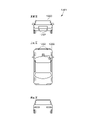
- the two photoelectric conversion devices 1302 are arranged in front of the vehicle 1300.
- the center line with respect to the advancing / retreating direction or the outer shape (for example, the vehicle width) of the vehicle 1300 is regarded as an axis of symmetry, and the two photoelectric conversion devices 1302 are arranged line-symmetrically with respect to the axis of symmetry, the vehicle 1300 and It is preferable for acquiring distance information with the object to be photographed and determining the possibility of collision.
- the photoelectric conversion device 1302 is arranged so as not to obstruct the driver's field of view when the driver visually recognizes the situation outside the vehicle 1300 from the driver's seat.
- a photoelectric conversion device 1302 may be arranged behind the vehicle 1300 to sound an alarm when a vehicle behind the vehicle approaches.
- the photoelectric conversion device can be applied to the control of automatically driving following other vehicles and the control of automatically driving so as not to go out of the lane.
- the photoelectric conversion system 1301 can be applied not only to a vehicle such as a own vehicle but also to a moving body (moving device) such as a ship, an aircraft, or an industrial robot.
- a moving body moving device
- it can be applied not only to moving objects but also to devices that widely use object recognition, such as intelligent transportation systems (ITS).
- ITS intelligent transportation systems
- the photoelectric conversion device of the present invention may further have a configuration capable of acquiring various information such as distance information.
Landscapes
- Engineering & Computer Science (AREA)
- Physics & Mathematics (AREA)
- Computer Networks & Wireless Communication (AREA)
- General Physics & Mathematics (AREA)
- Radar, Positioning & Navigation (AREA)
- Remote Sensing (AREA)
- Electromagnetism (AREA)
- Multimedia (AREA)
- Signal Processing (AREA)
- Optical Radar Systems And Details Thereof (AREA)
- Transforming Light Signals Into Electric Signals (AREA)
Priority Applications (5)
| Application Number | Priority Date | Filing Date | Title |
|---|---|---|---|
| EP21882696.4A EP4236298A4 (en) | 2020-10-21 | 2021-10-14 | Photoelectric conversion device and photoelectric conversion system |
| KR1020237016128A KR20230088423A (ko) | 2020-10-21 | 2021-10-14 | 광전변환장치, 광전변환 시스템 |
| CN202180072028.4A CN116349238B (zh) | 2020-10-21 | 2021-10-14 | 光电转换设备及光电转换系统 |
| US18/303,480 US12044802B2 (en) | 2020-10-21 | 2023-04-19 | Photoelectric conversion device and photoelectric conversion system comprising a control unit to set a third exposure period and a.fourth exposure period on a basis of light value comparison based on signal charge during first and second exposure periods |
| US18/747,766 US12422526B2 (en) | 2020-10-21 | 2024-06-19 | Photoelectric conversion device and photoelectric conversion system |
Applications Claiming Priority (2)
| Application Number | Priority Date | Filing Date | Title |
|---|---|---|---|
| JP2020176599A JP7721260B2 (ja) | 2020-10-21 | 2020-10-21 | 光電変換装置、光電変換システム |
| JP2020-176599 | 2020-10-21 |
Related Child Applications (1)
| Application Number | Title | Priority Date | Filing Date |
|---|---|---|---|
| US18/303,480 Continuation US12044802B2 (en) | 2020-10-21 | 2023-04-19 | Photoelectric conversion device and photoelectric conversion system comprising a control unit to set a third exposure period and a.fourth exposure period on a basis of light value comparison based on signal charge during first and second exposure periods |
Publications (1)
| Publication Number | Publication Date |
|---|---|
| WO2022085555A1 true WO2022085555A1 (ja) | 2022-04-28 |
Family
ID=81290860
Family Applications (1)
| Application Number | Title | Priority Date | Filing Date |
|---|---|---|---|
| PCT/JP2021/038032 Ceased WO2022085555A1 (ja) | 2020-10-21 | 2021-10-14 | 光電変換装置、光電変換システム |
Country Status (6)
| Country | Link |
|---|---|
| US (2) | US12044802B2 (enExample) |
| EP (1) | EP4236298A4 (enExample) |
| JP (1) | JP7721260B2 (enExample) |
| KR (1) | KR20230088423A (enExample) |
| CN (1) | CN116349238B (enExample) |
| WO (1) | WO2022085555A1 (enExample) |
Cited By (1)
| Publication number | Priority date | Publication date | Assignee | Title |
|---|---|---|---|---|
| WO2023243380A1 (en) * | 2022-06-15 | 2023-12-21 | Sony Semiconductor Solutions Corporation | Photon counting photodetector with motion detection |
Families Citing this family (4)
| Publication number | Priority date | Publication date | Assignee | Title |
|---|---|---|---|---|
| JP7721260B2 (ja) * | 2020-10-21 | 2025-08-12 | キヤノン株式会社 | 光電変換装置、光電変換システム |
| JP2024038655A (ja) * | 2022-09-08 | 2024-03-21 | キヤノン株式会社 | 光電変換装置 |
| CN119375897A (zh) * | 2023-07-25 | 2025-01-28 | 爱思开海力士有限公司 | 用于感测距离的图像感测装置 |
| JP2025091560A (ja) * | 2023-12-07 | 2025-06-19 | キヤノン株式会社 | 信号生成装置、信号生成システム |
Citations (5)
| Publication number | Priority date | Publication date | Assignee | Title |
|---|---|---|---|---|
| US20170052065A1 (en) | 2015-08-20 | 2017-02-23 | Apple Inc. | SPAD array with gated histogram construction |
| WO2017085916A1 (ja) * | 2015-11-16 | 2017-05-26 | パナソニックIpマネジメント株式会社 | 撮像装置、及びそれに用いられる固体撮像素子 |
| WO2019188348A1 (ja) * | 2018-03-29 | 2019-10-03 | パナソニックIpマネジメント株式会社 | 距離情報取得装置、マルチパス検出装置およびマルチパス検出方法 |
| WO2020027221A1 (ja) * | 2018-08-02 | 2020-02-06 | パナソニックIpマネジメント株式会社 | 撮像装置、及びそれに用いられる固体撮像素子 |
| JP2020176599A (ja) | 2019-04-22 | 2020-10-29 | ダイハツ工業株式会社 | 内燃機関 |
Family Cites Families (14)
| Publication number | Priority date | Publication date | Assignee | Title |
|---|---|---|---|---|
| JP6539990B2 (ja) * | 2014-11-14 | 2019-07-10 | 株式会社デンソー | 光飛行型測距装置 |
| DE102015110748A1 (de) | 2015-07-03 | 2017-01-05 | Schuler Pressen Gmbh | Verfahren zur Einstellung eines Phasenversatzes einer mehrfach wirkenden mechanischen Querwellenpresse sowie eine Presse nach diesem Verfahren |
| EP3334151B1 (en) * | 2015-08-04 | 2021-04-07 | Panasonic Semiconductor Solutions Co., Ltd. | Method for driving solid-state imaging device |
| KR102404260B1 (ko) | 2015-11-03 | 2022-05-30 | 삼성중공업 주식회사 | 밸러스트수 여과 필터 설치 장치 및 방법 |
| WO2017141957A1 (ja) * | 2016-02-17 | 2017-08-24 | パナソニックIpマネジメント株式会社 | 距離測定装置 |
| JPWO2017150246A1 (ja) * | 2016-02-29 | 2018-12-27 | パナソニックIpマネジメント株式会社 | 撮像装置、及びそれに用いられる固体撮像素子 |
| KR102673812B1 (ko) * | 2016-07-26 | 2024-06-10 | 삼성전자주식회사 | 라이다 장치 및 거리 측정 방법 |
| US10880503B2 (en) | 2016-10-03 | 2020-12-29 | Sony Semiconductor Solutions Corporation | Solid-state image pickup device and image pickup method, and electronic apparatus |
| JP7157529B2 (ja) * | 2017-12-25 | 2022-10-20 | キヤノン株式会社 | 撮像装置、撮像システム、および撮像装置の駆動方法 |
| US10598936B1 (en) * | 2018-04-23 | 2020-03-24 | Facebook Technologies, Llc | Multi-mode active pixel sensor |
| JP7129264B2 (ja) | 2018-08-03 | 2022-09-01 | キヤノン株式会社 | 撮像装置 |
| JP7218191B2 (ja) | 2019-01-30 | 2023-02-06 | キヤノン株式会社 | 光電変換装置、撮像システム、移動体 |
| EP3879291A1 (fr) | 2020-03-13 | 2021-09-15 | Hervé Sallin | Dispositif de contrôle d'installations électriques |
| JP7721260B2 (ja) * | 2020-10-21 | 2025-08-12 | キヤノン株式会社 | 光電変換装置、光電変換システム |
-
2020
- 2020-10-21 JP JP2020176599A patent/JP7721260B2/ja active Active
-
2021
- 2021-10-14 CN CN202180072028.4A patent/CN116349238B/zh active Active
- 2021-10-14 EP EP21882696.4A patent/EP4236298A4/en active Pending
- 2021-10-14 KR KR1020237016128A patent/KR20230088423A/ko active Pending
- 2021-10-14 WO PCT/JP2021/038032 patent/WO2022085555A1/ja not_active Ceased
-
2023
- 2023-04-19 US US18/303,480 patent/US12044802B2/en active Active
-
2024
- 2024-06-19 US US18/747,766 patent/US12422526B2/en active Active
Patent Citations (5)
| Publication number | Priority date | Publication date | Assignee | Title |
|---|---|---|---|---|
| US20170052065A1 (en) | 2015-08-20 | 2017-02-23 | Apple Inc. | SPAD array with gated histogram construction |
| WO2017085916A1 (ja) * | 2015-11-16 | 2017-05-26 | パナソニックIpマネジメント株式会社 | 撮像装置、及びそれに用いられる固体撮像素子 |
| WO2019188348A1 (ja) * | 2018-03-29 | 2019-10-03 | パナソニックIpマネジメント株式会社 | 距離情報取得装置、マルチパス検出装置およびマルチパス検出方法 |
| WO2020027221A1 (ja) * | 2018-08-02 | 2020-02-06 | パナソニックIpマネジメント株式会社 | 撮像装置、及びそれに用いられる固体撮像素子 |
| JP2020176599A (ja) | 2019-04-22 | 2020-10-29 | ダイハツ工業株式会社 | 内燃機関 |
Non-Patent Citations (1)
| Title |
|---|
| See also references of EP4236298A4 |
Cited By (1)
| Publication number | Priority date | Publication date | Assignee | Title |
|---|---|---|---|---|
| WO2023243380A1 (en) * | 2022-06-15 | 2023-12-21 | Sony Semiconductor Solutions Corporation | Photon counting photodetector with motion detection |
Also Published As
| Publication number | Publication date |
|---|---|
| US12422526B2 (en) | 2025-09-23 |
| CN116349238B (zh) | 2025-08-01 |
| US20240337731A1 (en) | 2024-10-10 |
| EP4236298A1 (en) | 2023-08-30 |
| US20230258776A1 (en) | 2023-08-17 |
| US12044802B2 (en) | 2024-07-23 |
| JP7721260B2 (ja) | 2025-08-12 |
| EP4236298A4 (en) | 2024-09-25 |
| JP2022067801A (ja) | 2022-05-09 |
| KR20230088423A (ko) | 2023-06-19 |
| CN116349238A (zh) | 2023-06-27 |
Similar Documents
| Publication | Publication Date | Title |
|---|---|---|
| JP7721260B2 (ja) | 光電変換装置、光電変換システム | |
| US9171985B2 (en) | Pixel circuit with controlled capacitor discharge time of flight measurement | |
| JP7630985B2 (ja) | 光電変換装置及びその駆動方法 | |
| US10833207B2 (en) | Photo-detection device, photo-detection system, and mobile apparatus | |
| JP7527853B2 (ja) | 光電変換装置 | |
| JP7353765B2 (ja) | 光検出装置、光検出システム及び移動体 | |
| JP7117535B2 (ja) | 固体撮像素子及び撮像システム | |
| JP7089390B2 (ja) | 光電変換装置及びその駆動方法 | |
| JP2020162109A (ja) | 光電変換装置、光電変換システム、および移動体 | |
| JP6735515B2 (ja) | 固体撮像装置 | |
| JP2020107980A (ja) | 光検出装置および撮像システム | |
| JP7604204B2 (ja) | 光電変換装置、撮像システム、移動体 | |
| US11818488B2 (en) | Photoelectric conversion device, photoelectric conversion system, and moving body | |
| US11965987B2 (en) | Solid-state imaging device, distance measuring device, and distance measuring method | |
| US20240004037A1 (en) | Distance measuring device and solid-state imaging device | |
| US20250102644A1 (en) | Tdc device and ranging apparatus | |
| JP2024090470A (ja) | 光電変換装置及び信号処理装置 | |
| JP2025091560A (ja) | 信号生成装置、信号生成システム | |
| WO2025204825A1 (ja) | 光電変換装置、撮像システム、移動体 |
Legal Events
| Date | Code | Title | Description |
|---|---|---|---|
| 121 | Ep: the epo has been informed by wipo that ep was designated in this application |
Ref document number: 21882696 Country of ref document: EP Kind code of ref document: A1 |
|
| ENP | Entry into the national phase |
Ref document number: 20237016128 Country of ref document: KR Kind code of ref document: A |
|
| NENP | Non-entry into the national phase |
Ref country code: DE |
|
| ENP | Entry into the national phase |
Ref document number: 2021882696 Country of ref document: EP Effective date: 20230522 |
|
| WWG | Wipo information: grant in national office |
Ref document number: 202180072028.4 Country of ref document: CN |