WO2022084800A1 - Dispositif à semi-conducteur et appareil électronique - Google Patents
Dispositif à semi-conducteur et appareil électronique Download PDFInfo
- Publication number
- WO2022084800A1 WO2022084800A1 PCT/IB2021/059303 IB2021059303W WO2022084800A1 WO 2022084800 A1 WO2022084800 A1 WO 2022084800A1 IB 2021059303 W IB2021059303 W IB 2021059303W WO 2022084800 A1 WO2022084800 A1 WO 2022084800A1
- Authority
- WO
- WIPO (PCT)
- Prior art keywords
- insulator
- transistor
- oxide
- conductor
- memory cell
- Prior art date
Links
- 239000004065 semiconductor Substances 0.000 title claims abstract description 324
- 230000006870 function Effects 0.000 claims description 176
- 229910044991 metal oxide Inorganic materials 0.000 claims description 76
- 150000004706 metal oxides Chemical class 0.000 claims description 75
- 238000004364 calculation method Methods 0.000 claims description 27
- 229910000449 hafnium oxide Inorganic materials 0.000 claims description 26
- WIHZLLGSGQNAGK-UHFFFAOYSA-N hafnium(4+);oxygen(2-) Chemical compound [O-2].[O-2].[Hf+4] WIHZLLGSGQNAGK-UHFFFAOYSA-N 0.000 claims description 26
- RVTZCBVAJQQJTK-UHFFFAOYSA-N oxygen(2-);zirconium(4+) Chemical compound [O-2].[O-2].[Zr+4] RVTZCBVAJQQJTK-UHFFFAOYSA-N 0.000 claims description 15
- 229910001928 zirconium oxide Inorganic materials 0.000 claims description 15
- 239000003990 capacitor Substances 0.000 abstract description 17
- 239000012212 insulator Substances 0.000 description 804
- 239000004020 conductor Substances 0.000 description 439
- 210000004027 cell Anatomy 0.000 description 173
- 239000010408 film Substances 0.000 description 165
- 239000010410 layer Substances 0.000 description 162
- 229910052760 oxygen Inorganic materials 0.000 description 116
- 229910052739 hydrogen Inorganic materials 0.000 description 115
- 239000001257 hydrogen Substances 0.000 description 113
- 239000000463 material Substances 0.000 description 113
- 239000001301 oxygen Substances 0.000 description 112
- QVGXLLKOCUKJST-UHFFFAOYSA-N atomic oxygen Chemical compound [O] QVGXLLKOCUKJST-UHFFFAOYSA-N 0.000 description 110
- UFHFLCQGNIYNRP-UHFFFAOYSA-N Hydrogen Chemical compound [H][H] UFHFLCQGNIYNRP-UHFFFAOYSA-N 0.000 description 100
- 238000000034 method Methods 0.000 description 86
- 239000000758 substrate Substances 0.000 description 75
- 239000012535 impurity Substances 0.000 description 69
- 239000013078 crystal Substances 0.000 description 64
- 239000000523 sample Substances 0.000 description 60
- 230000005621 ferroelectricity Effects 0.000 description 54
- IJGRMHOSHXDMSA-UHFFFAOYSA-N Atomic nitrogen Chemical compound N#N IJGRMHOSHXDMSA-UHFFFAOYSA-N 0.000 description 46
- 230000004888 barrier function Effects 0.000 description 44
- XUIMIQQOPSSXEZ-UHFFFAOYSA-N Silicon Chemical compound [Si] XUIMIQQOPSSXEZ-UHFFFAOYSA-N 0.000 description 39
- 229910052710 silicon Inorganic materials 0.000 description 39
- 239000010703 silicon Substances 0.000 description 39
- 238000010586 diagram Methods 0.000 description 38
- 229910052814 silicon oxide Inorganic materials 0.000 description 36
- 239000011701 zinc Substances 0.000 description 36
- VYPSYNLAJGMNEJ-UHFFFAOYSA-N silicon dioxide Inorganic materials O=[Si]=O VYPSYNLAJGMNEJ-UHFFFAOYSA-N 0.000 description 35
- 229910052581 Si3N4 Inorganic materials 0.000 description 34
- 230000010287 polarization Effects 0.000 description 33
- 238000000231 atomic layer deposition Methods 0.000 description 31
- 229910001868 water Inorganic materials 0.000 description 31
- 125000004429 atom Chemical group 0.000 description 30
- 238000009792 diffusion process Methods 0.000 description 30
- HQVNEWCFYHHQES-UHFFFAOYSA-N silicon nitride Chemical compound N12[Si]34N5[Si]62N3[Si]51N64 HQVNEWCFYHHQES-UHFFFAOYSA-N 0.000 description 30
- 229910052735 hafnium Inorganic materials 0.000 description 29
- 150000004767 nitrides Chemical class 0.000 description 28
- TWNQGVIAIRXVLR-UHFFFAOYSA-N oxo(oxoalumanyloxy)alumane Chemical compound O=[Al]O[Al]=O TWNQGVIAIRXVLR-UHFFFAOYSA-N 0.000 description 28
- 229910052782 aluminium Inorganic materials 0.000 description 27
- XAGFODPZIPBFFR-UHFFFAOYSA-N aluminium Chemical compound [Al] XAGFODPZIPBFFR-UHFFFAOYSA-N 0.000 description 27
- XLYOFNOQVPJJNP-UHFFFAOYSA-N water Substances O XLYOFNOQVPJJNP-UHFFFAOYSA-N 0.000 description 27
- 230000005684 electric field Effects 0.000 description 26
- 229910052751 metal Inorganic materials 0.000 description 26
- 235000012431 wafers Nutrition 0.000 description 25
- 230000015572 biosynthetic process Effects 0.000 description 24
- VBJZVLUMGGDVMO-UHFFFAOYSA-N hafnium atom Chemical group [Hf] VBJZVLUMGGDVMO-UHFFFAOYSA-N 0.000 description 24
- 238000003860 storage Methods 0.000 description 24
- 229910052757 nitrogen Inorganic materials 0.000 description 23
- 239000002184 metal Substances 0.000 description 22
- 238000005259 measurement Methods 0.000 description 21
- -1 metal oxide nitride Chemical class 0.000 description 20
- 239000000203 mixture Substances 0.000 description 20
- 229910052721 tungsten Inorganic materials 0.000 description 20
- 239000010937 tungsten Substances 0.000 description 20
- 206010021143 Hypoxia Diseases 0.000 description 19
- WFKWXMTUELFFGS-UHFFFAOYSA-N tungsten Chemical compound [W] WFKWXMTUELFFGS-UHFFFAOYSA-N 0.000 description 19
- 230000003071 parasitic effect Effects 0.000 description 18
- 230000007547 defect Effects 0.000 description 17
- 150000002431 hydrogen Chemical class 0.000 description 17
- 238000010438 heat treatment Methods 0.000 description 16
- OKTJSMMVPCPJKN-UHFFFAOYSA-N Carbon Chemical compound [C] OKTJSMMVPCPJKN-UHFFFAOYSA-N 0.000 description 15
- 230000008859 change Effects 0.000 description 15
- 230000007423 decrease Effects 0.000 description 15
- 238000004519 manufacturing process Methods 0.000 description 15
- 239000002356 single layer Substances 0.000 description 15
- 229910052799 carbon Inorganic materials 0.000 description 14
- 239000003989 dielectric material Substances 0.000 description 13
- 238000004544 sputter deposition Methods 0.000 description 13
- 239000010936 titanium Substances 0.000 description 13
- RTAQQCXQSZGOHL-UHFFFAOYSA-N Titanium Chemical compound [Ti] RTAQQCXQSZGOHL-UHFFFAOYSA-N 0.000 description 12
- 239000012298 atmosphere Substances 0.000 description 12
- 229910052738 indium Inorganic materials 0.000 description 12
- 239000002243 precursor Substances 0.000 description 12
- 229910052719 titanium Inorganic materials 0.000 description 12
- RYGMFSIKBFXOCR-UHFFFAOYSA-N Copper Chemical compound [Cu] RYGMFSIKBFXOCR-UHFFFAOYSA-N 0.000 description 11
- 230000007812 deficiency Effects 0.000 description 11
- 238000013461 design Methods 0.000 description 11
- 230000000694 effects Effects 0.000 description 11
- 229910052715 tantalum Inorganic materials 0.000 description 11
- GUVRBAGPIYLISA-UHFFFAOYSA-N tantalum atom Chemical compound [Ta] GUVRBAGPIYLISA-UHFFFAOYSA-N 0.000 description 11
- NRTOMJZYCJJWKI-UHFFFAOYSA-N Titanium nitride Chemical compound [Ti]#N NRTOMJZYCJJWKI-UHFFFAOYSA-N 0.000 description 10
- 230000005669 field effect Effects 0.000 description 10
- 229910052733 gallium Inorganic materials 0.000 description 10
- APFVFJFRJDLVQX-UHFFFAOYSA-N indium atom Chemical compound [In] APFVFJFRJDLVQX-UHFFFAOYSA-N 0.000 description 10
- 239000004215 Carbon black (E152) Substances 0.000 description 9
- MWUXSHHQAYIFBG-UHFFFAOYSA-N Nitric oxide Chemical compound O=[N] MWUXSHHQAYIFBG-UHFFFAOYSA-N 0.000 description 9
- 239000010949 copper Substances 0.000 description 9
- 229930195733 hydrocarbon Natural products 0.000 description 9
- 150000002430 hydrocarbons Chemical class 0.000 description 9
- 239000007800 oxidant agent Substances 0.000 description 9
- 239000000126 substance Substances 0.000 description 9
- MZLGASXMSKOWSE-UHFFFAOYSA-N tantalum nitride Chemical compound [Ta]#N MZLGASXMSKOWSE-UHFFFAOYSA-N 0.000 description 9
- GYHNNYVSQQEPJS-UHFFFAOYSA-N Gallium Chemical compound [Ga] GYHNNYVSQQEPJS-UHFFFAOYSA-N 0.000 description 8
- PXHVJJICTQNCMI-UHFFFAOYSA-N Nickel Chemical group [Ni] PXHVJJICTQNCMI-UHFFFAOYSA-N 0.000 description 8
- 229910052802 copper Inorganic materials 0.000 description 8
- PMHQVHHXPFUNSP-UHFFFAOYSA-M copper(1+);methylsulfanylmethane;bromide Chemical compound Br[Cu].CSC PMHQVHHXPFUNSP-UHFFFAOYSA-M 0.000 description 8
- 239000010409 thin film Substances 0.000 description 8
- 229910052727 yttrium Inorganic materials 0.000 description 8
- VWQVUPCCIRVNHF-UHFFFAOYSA-N yttrium atom Chemical compound [Y] VWQVUPCCIRVNHF-UHFFFAOYSA-N 0.000 description 8
- 230000009471 action Effects 0.000 description 7
- 239000011229 interlayer Substances 0.000 description 7
- 125000004430 oxygen atom Chemical group O* 0.000 description 7
- 238000001004 secondary ion mass spectrometry Methods 0.000 description 7
- 238000001228 spectrum Methods 0.000 description 7
- 229910052712 strontium Inorganic materials 0.000 description 7
- XEEYBQQBJWHFJM-UHFFFAOYSA-N Iron Chemical group [Fe] XEEYBQQBJWHFJM-UHFFFAOYSA-N 0.000 description 6
- ZOKXTWBITQBERF-UHFFFAOYSA-N Molybdenum Chemical compound [Mo] ZOKXTWBITQBERF-UHFFFAOYSA-N 0.000 description 6
- 238000005229 chemical vapour deposition Methods 0.000 description 6
- 238000002003 electron diffraction Methods 0.000 description 6
- 229910003437 indium oxide Inorganic materials 0.000 description 6
- PJXISJQVUVHSOJ-UHFFFAOYSA-N indium(iii) oxide Chemical compound [O-2].[O-2].[O-2].[In+3].[In+3] PJXISJQVUVHSOJ-UHFFFAOYSA-N 0.000 description 6
- 229910052746 lanthanum Inorganic materials 0.000 description 6
- FZLIPJUXYLNCLC-UHFFFAOYSA-N lanthanum atom Chemical compound [La] FZLIPJUXYLNCLC-UHFFFAOYSA-N 0.000 description 6
- 229910052451 lead zirconate titanate Inorganic materials 0.000 description 6
- CPLXHLVBOLITMK-UHFFFAOYSA-N magnesium oxide Inorganic materials [Mg]=O CPLXHLVBOLITMK-UHFFFAOYSA-N 0.000 description 6
- 239000012528 membrane Substances 0.000 description 6
- 229910052750 molybdenum Inorganic materials 0.000 description 6
- 239000011733 molybdenum Substances 0.000 description 6
- 230000008569 process Effects 0.000 description 6
- 238000012360 testing method Methods 0.000 description 6
- ZOXJGFHDIHLPTG-UHFFFAOYSA-N Boron Chemical compound [B] ZOXJGFHDIHLPTG-UHFFFAOYSA-N 0.000 description 5
- MYMOFIZGZYHOMD-UHFFFAOYSA-N Dioxygen Chemical compound O=O MYMOFIZGZYHOMD-UHFFFAOYSA-N 0.000 description 5
- QCWXUUIWCKQGHC-UHFFFAOYSA-N Zirconium Chemical group [Zr] QCWXUUIWCKQGHC-UHFFFAOYSA-N 0.000 description 5
- 229910052796 boron Inorganic materials 0.000 description 5
- 239000000969 carrier Substances 0.000 description 5
- 230000006378 damage Effects 0.000 description 5
- 238000010894 electron beam technology Methods 0.000 description 5
- 125000004435 hydrogen atom Chemical group [H]* 0.000 description 5
- 239000000395 magnesium oxide Substances 0.000 description 5
- 239000007769 metal material Substances 0.000 description 5
- 239000002159 nanocrystal Substances 0.000 description 5
- 230000003647 oxidation Effects 0.000 description 5
- 238000007254 oxidation reaction Methods 0.000 description 5
- 230000000717 retained effect Effects 0.000 description 5
- 229910052707 ruthenium Inorganic materials 0.000 description 5
- 238000000926 separation method Methods 0.000 description 5
- CIOAGBVUUVVLOB-UHFFFAOYSA-N strontium atom Chemical compound [Sr] CIOAGBVUUVVLOB-UHFFFAOYSA-N 0.000 description 5
- OGIDPMRJRNCKJF-UHFFFAOYSA-N titanium oxide Inorganic materials [Ti]=O OGIDPMRJRNCKJF-UHFFFAOYSA-N 0.000 description 5
- 229910052725 zinc Inorganic materials 0.000 description 5
- 229910052726 zirconium Inorganic materials 0.000 description 5
- JBRZTFJDHDCESZ-UHFFFAOYSA-N AsGa Chemical compound [As]#[Ga] JBRZTFJDHDCESZ-UHFFFAOYSA-N 0.000 description 4
- 229910001218 Gallium arsenide Inorganic materials 0.000 description 4
- 229910052779 Neodymium Inorganic materials 0.000 description 4
- KJTLSVCANCCWHF-UHFFFAOYSA-N Ruthenium Chemical compound [Ru] KJTLSVCANCCWHF-UHFFFAOYSA-N 0.000 description 4
- ATJFFYVFTNAWJD-UHFFFAOYSA-N Tin Chemical group [Sn] ATJFFYVFTNAWJD-UHFFFAOYSA-N 0.000 description 4
- XLOMVQKBTHCTTD-UHFFFAOYSA-N Zinc monoxide Chemical compound [Zn]=O XLOMVQKBTHCTTD-UHFFFAOYSA-N 0.000 description 4
- 229910052783 alkali metal Inorganic materials 0.000 description 4
- 150000001340 alkali metals Chemical class 0.000 description 4
- 229910052784 alkaline earth metal Inorganic materials 0.000 description 4
- 150000001342 alkaline earth metals Chemical class 0.000 description 4
- 230000008878 coupling Effects 0.000 description 4
- 238000010168 coupling process Methods 0.000 description 4
- 238000005859 coupling reaction Methods 0.000 description 4
- AJNVQOSZGJRYEI-UHFFFAOYSA-N digallium;oxygen(2-) Chemical compound [O-2].[O-2].[O-2].[Ga+3].[Ga+3] AJNVQOSZGJRYEI-UHFFFAOYSA-N 0.000 description 4
- 238000002149 energy-dispersive X-ray emission spectroscopy Methods 0.000 description 4
- 229910001195 gallium oxide Inorganic materials 0.000 description 4
- 239000007789 gas Substances 0.000 description 4
- 239000011521 glass Substances 0.000 description 4
- 230000020169 heat generation Effects 0.000 description 4
- 239000011810 insulating material Substances 0.000 description 4
- 238000009413 insulation Methods 0.000 description 4
- 230000010354 integration Effects 0.000 description 4
- 239000011777 magnesium Substances 0.000 description 4
- AXZKOIWUVFPNLO-UHFFFAOYSA-N magnesium;oxygen(2-) Chemical compound [O-2].[Mg+2] AXZKOIWUVFPNLO-UHFFFAOYSA-N 0.000 description 4
- QEFYFXOXNSNQGX-UHFFFAOYSA-N neodymium atom Chemical compound [Nd] QEFYFXOXNSNQGX-UHFFFAOYSA-N 0.000 description 4
- 229910052759 nickel Inorganic materials 0.000 description 4
- BPUBBGLMJRNUCC-UHFFFAOYSA-N oxygen(2-);tantalum(5+) Chemical compound [O-2].[O-2].[O-2].[O-2].[O-2].[Ta+5].[Ta+5] BPUBBGLMJRNUCC-UHFFFAOYSA-N 0.000 description 4
- 230000002093 peripheral effect Effects 0.000 description 4
- 239000012466 permeate Substances 0.000 description 4
- 229910001925 ruthenium oxide Inorganic materials 0.000 description 4
- WOCIAKWEIIZHES-UHFFFAOYSA-N ruthenium(iv) oxide Chemical compound O=[Ru]=O WOCIAKWEIIZHES-UHFFFAOYSA-N 0.000 description 4
- 229910052718 tin Inorganic materials 0.000 description 4
- 229910052684 Cerium Inorganic materials 0.000 description 3
- ZAMOUSCENKQFHK-UHFFFAOYSA-N Chlorine atom Chemical compound [Cl] ZAMOUSCENKQFHK-UHFFFAOYSA-N 0.000 description 3
- 229910002601 GaN Inorganic materials 0.000 description 3
- JMASRVWKEDWRBT-UHFFFAOYSA-N Gallium nitride Chemical compound [Ga]#N JMASRVWKEDWRBT-UHFFFAOYSA-N 0.000 description 3
- FYYHWMGAXLPEAU-UHFFFAOYSA-N Magnesium Chemical compound [Mg] FYYHWMGAXLPEAU-UHFFFAOYSA-N 0.000 description 3
- 101150075681 SCL1 gene Proteins 0.000 description 3
- 229910000577 Silicon-germanium Inorganic materials 0.000 description 3
- GWEVSGVZZGPLCZ-UHFFFAOYSA-N Titan oxide Chemical compound O=[Ti]=O GWEVSGVZZGPLCZ-UHFFFAOYSA-N 0.000 description 3
- 238000004833 X-ray photoelectron spectroscopy Methods 0.000 description 3
- HCHKCACWOHOZIP-UHFFFAOYSA-N Zinc Chemical compound [Zn] HCHKCACWOHOZIP-UHFFFAOYSA-N 0.000 description 3
- 239000000956 alloy Substances 0.000 description 3
- 238000000137 annealing Methods 0.000 description 3
- 229910052788 barium Inorganic materials 0.000 description 3
- 239000002585 base Substances 0.000 description 3
- GWXLDORMOJMVQZ-UHFFFAOYSA-N cerium Chemical compound [Ce] GWXLDORMOJMVQZ-UHFFFAOYSA-N 0.000 description 3
- 238000006243 chemical reaction Methods 0.000 description 3
- 239000000460 chlorine Substances 0.000 description 3
- 229910052801 chlorine Inorganic materials 0.000 description 3
- 239000011651 chromium Substances 0.000 description 3
- 238000004891 communication Methods 0.000 description 3
- 150000001875 compounds Chemical class 0.000 description 3
- 238000005520 cutting process Methods 0.000 description 3
- 229910001873 dinitrogen Inorganic materials 0.000 description 3
- 229910052732 germanium Inorganic materials 0.000 description 3
- GNPVGFCGXDBREM-UHFFFAOYSA-N germanium atom Chemical compound [Ge] GNPVGFCGXDBREM-UHFFFAOYSA-N 0.000 description 3
- AMGQUBHHOARCQH-UHFFFAOYSA-N indium;oxotin Chemical compound [In].[Sn]=O AMGQUBHHOARCQH-UHFFFAOYSA-N 0.000 description 3
- 239000011261 inert gas Substances 0.000 description 3
- 229910052742 iron Inorganic materials 0.000 description 3
- HFGPZNIAWCZYJU-UHFFFAOYSA-N lead zirconate titanate Chemical compound [O-2].[O-2].[O-2].[O-2].[O-2].[Ti+4].[Zr+4].[Pb+2] HFGPZNIAWCZYJU-UHFFFAOYSA-N 0.000 description 3
- 229910052749 magnesium Inorganic materials 0.000 description 3
- 239000011159 matrix material Substances 0.000 description 3
- 238000012986 modification Methods 0.000 description 3
- 230000004048 modification Effects 0.000 description 3
- 125000004433 nitrogen atom Chemical group N* 0.000 description 3
- QGLKJKCYBOYXKC-UHFFFAOYSA-N nonaoxidotritungsten Chemical compound O=[W]1(=O)O[W](=O)(=O)O[W](=O)(=O)O1 QGLKJKCYBOYXKC-UHFFFAOYSA-N 0.000 description 3
- 230000001151 other effect Effects 0.000 description 3
- 230000001590 oxidative effect Effects 0.000 description 3
- 239000004033 plastic Substances 0.000 description 3
- 229920003023 plastic Polymers 0.000 description 3
- 238000012545 processing Methods 0.000 description 3
- 229910052706 scandium Inorganic materials 0.000 description 3
- SIXSYDAISGFNSX-UHFFFAOYSA-N scandium atom Chemical compound [Sc] SIXSYDAISGFNSX-UHFFFAOYSA-N 0.000 description 3
- VEALVRVVWBQVSL-UHFFFAOYSA-N strontium titanate Chemical compound [Sr+2].[O-][Ti]([O-])=O VEALVRVVWBQVSL-UHFFFAOYSA-N 0.000 description 3
- 229910001936 tantalum oxide Inorganic materials 0.000 description 3
- 229910001930 tungsten oxide Inorganic materials 0.000 description 3
- YVTHLONGBIQYBO-UHFFFAOYSA-N zinc indium(3+) oxygen(2-) Chemical compound [O--].[Zn++].[In+3] YVTHLONGBIQYBO-UHFFFAOYSA-N 0.000 description 3
- VYZAMTAEIAYCRO-UHFFFAOYSA-N Chromium Chemical compound [Cr] VYZAMTAEIAYCRO-UHFFFAOYSA-N 0.000 description 2
- PXGOKWXKJXAPGV-UHFFFAOYSA-N Fluorine Chemical compound FF PXGOKWXKJXAPGV-UHFFFAOYSA-N 0.000 description 2
- 229910052688 Gadolinium Inorganic materials 0.000 description 2
- GQPLMRYTRLFLPF-UHFFFAOYSA-N Nitrous Oxide Chemical compound [O-][N+]#N GQPLMRYTRLFLPF-UHFFFAOYSA-N 0.000 description 2
- BPQQTUXANYXVAA-UHFFFAOYSA-N Orthosilicate Chemical compound [O-][Si]([O-])([O-])[O-] BPQQTUXANYXVAA-UHFFFAOYSA-N 0.000 description 2
- OAICVXFJPJFONN-UHFFFAOYSA-N Phosphorus Chemical compound [P] OAICVXFJPJFONN-UHFFFAOYSA-N 0.000 description 2
- 238000002441 X-ray diffraction Methods 0.000 description 2
- 229910007926 ZrCl Inorganic materials 0.000 description 2
- 229910021417 amorphous silicon Inorganic materials 0.000 description 2
- 238000004458 analytical method Methods 0.000 description 2
- 229910052785 arsenic Inorganic materials 0.000 description 2
- RQNWIZPPADIBDY-UHFFFAOYSA-N arsenic atom Chemical compound [As] RQNWIZPPADIBDY-UHFFFAOYSA-N 0.000 description 2
- JRPBQTZRNDNNOP-UHFFFAOYSA-N barium titanate Chemical compound [Ba+2].[Ba+2].[O-][Ti]([O-])([O-])[O-] JRPBQTZRNDNNOP-UHFFFAOYSA-N 0.000 description 2
- 229910002113 barium titanate Inorganic materials 0.000 description 2
- 230000000903 blocking effect Effects 0.000 description 2
- 239000011575 calcium Substances 0.000 description 2
- 239000000919 ceramic Substances 0.000 description 2
- 229910052804 chromium Inorganic materials 0.000 description 2
- 239000002131 composite material Substances 0.000 description 2
- 238000002425 crystallisation Methods 0.000 description 2
- 230000008025 crystallization Effects 0.000 description 2
- 238000003795 desorption Methods 0.000 description 2
- 238000002524 electron diffraction data Methods 0.000 description 2
- 230000001747 exhibiting effect Effects 0.000 description 2
- 239000011737 fluorine Substances 0.000 description 2
- 229910052731 fluorine Inorganic materials 0.000 description 2
- 239000011888 foil Substances 0.000 description 2
- UIWYJDYFSGRHKR-UHFFFAOYSA-N gadolinium atom Chemical compound [Gd] UIWYJDYFSGRHKR-UHFFFAOYSA-N 0.000 description 2
- 238000002347 injection Methods 0.000 description 2
- 239000007924 injection Substances 0.000 description 2
- 150000002500 ions Chemical class 0.000 description 2
- 238000010030 laminating Methods 0.000 description 2
- 238000002156 mixing Methods 0.000 description 2
- 229910021421 monocrystalline silicon Inorganic materials 0.000 description 2
- 239000010955 niobium Substances 0.000 description 2
- 229910052698 phosphorus Inorganic materials 0.000 description 2
- 239000011574 phosphorus Substances 0.000 description 2
- 230000000704 physical effect Effects 0.000 description 2
- 229920000139 polyethylene terephthalate Polymers 0.000 description 2
- 239000005020 polyethylene terephthalate Substances 0.000 description 2
- 229920001343 polytetrafluoroethylene Polymers 0.000 description 2
- 239000004810 polytetrafluoroethylene Substances 0.000 description 2
- 239000011148 porous material Substances 0.000 description 2
- 238000004549 pulsed laser deposition Methods 0.000 description 2
- 230000009467 reduction Effects 0.000 description 2
- 239000011819 refractory material Substances 0.000 description 2
- 229920005989 resin Polymers 0.000 description 2
- 239000011347 resin Substances 0.000 description 2
- 210000005245 right atrium Anatomy 0.000 description 2
- 210000005241 right ventricle Anatomy 0.000 description 2
- 238000000851 scanning transmission electron micrograph Methods 0.000 description 2
- 101150081985 scrib gene Proteins 0.000 description 2
- VSZWPYCFIRKVQL-UHFFFAOYSA-N selanylidenegallium;selenium Chemical group [Se].[Se]=[Ga].[Se]=[Ga] VSZWPYCFIRKVQL-UHFFFAOYSA-N 0.000 description 2
- 229910000679 solder Inorganic materials 0.000 description 2
- 238000005476 soldering Methods 0.000 description 2
- 239000010935 stainless steel Substances 0.000 description 2
- 229910001220 stainless steel Inorganic materials 0.000 description 2
- 238000012916 structural analysis Methods 0.000 description 2
- 210000001321 subclavian vein Anatomy 0.000 description 2
- 239000013589 supplement Substances 0.000 description 2
- JBQYATWDVHIOAR-UHFFFAOYSA-N tellanylidenegermanium Chemical compound [Te]=[Ge] JBQYATWDVHIOAR-UHFFFAOYSA-N 0.000 description 2
- 239000011787 zinc oxide Substances 0.000 description 2
- 210000002925 A-like Anatomy 0.000 description 1
- OYPRJOBELJOOCE-UHFFFAOYSA-N Calcium Chemical compound [Ca] OYPRJOBELJOOCE-UHFFFAOYSA-N 0.000 description 1
- 239000004593 Epoxy Substances 0.000 description 1
- 229910052693 Europium Inorganic materials 0.000 description 1
- 235000015842 Hesperis Nutrition 0.000 description 1
- 235000012633 Iberis amara Nutrition 0.000 description 1
- GPXJNWSHGFTCBW-UHFFFAOYSA-N Indium phosphide Chemical compound [In]#P GPXJNWSHGFTCBW-UHFFFAOYSA-N 0.000 description 1
- 240000007594 Oryza sativa Species 0.000 description 1
- 235000007164 Oryza sativa Nutrition 0.000 description 1
- 229920012266 Poly(ether sulfone) PES Polymers 0.000 description 1
- 239000004952 Polyamide Substances 0.000 description 1
- 239000004642 Polyimide Substances 0.000 description 1
- 239000004743 Polypropylene Substances 0.000 description 1
- LEVVHYCKPQWKOP-UHFFFAOYSA-N [Si].[Ge] Chemical compound [Si].[Ge] LEVVHYCKPQWKOP-UHFFFAOYSA-N 0.000 description 1
- NIXOWILDQLNWCW-UHFFFAOYSA-N acrylic acid group Chemical group C(C=C)(=O)O NIXOWILDQLNWCW-UHFFFAOYSA-N 0.000 description 1
- 229910045601 alloy Inorganic materials 0.000 description 1
- MDPILPRLPQYEEN-UHFFFAOYSA-N aluminium arsenide Chemical compound [As]#[Al] MDPILPRLPQYEEN-UHFFFAOYSA-N 0.000 description 1
- PNEYBMLMFCGWSK-UHFFFAOYSA-N aluminium oxide Inorganic materials [O-2].[O-2].[O-2].[Al+3].[Al+3] PNEYBMLMFCGWSK-UHFFFAOYSA-N 0.000 description 1
- 239000005407 aluminoborosilicate glass Substances 0.000 description 1
- 230000003321 amplification Effects 0.000 description 1
- 229920003235 aromatic polyamide Polymers 0.000 description 1
- 238000013473 artificial intelligence Methods 0.000 description 1
- 238000013528 artificial neural network Methods 0.000 description 1
- GPBUGPUPKAGMDK-UHFFFAOYSA-N azanylidynemolybdenum Chemical compound [Mo]#N GPBUGPUPKAGMDK-UHFFFAOYSA-N 0.000 description 1
- DSAJWYNOEDNPEQ-UHFFFAOYSA-N barium atom Chemical compound [Ba] DSAJWYNOEDNPEQ-UHFFFAOYSA-N 0.000 description 1
- 229910052790 beryllium Inorganic materials 0.000 description 1
- ATBAMAFKBVZNFJ-UHFFFAOYSA-N beryllium atom Chemical group [Be] ATBAMAFKBVZNFJ-UHFFFAOYSA-N 0.000 description 1
- 230000005540 biological transmission Effects 0.000 description 1
- 229910052797 bismuth Inorganic materials 0.000 description 1
- JCXGWMGPZLAOME-UHFFFAOYSA-N bismuth atom Chemical compound [Bi] JCXGWMGPZLAOME-UHFFFAOYSA-N 0.000 description 1
- 229910000416 bismuth oxide Inorganic materials 0.000 description 1
- 230000036760 body temperature Effects 0.000 description 1
- 229910052795 boron group element Inorganic materials 0.000 description 1
- 239000005388 borosilicate glass Substances 0.000 description 1
- 229910052793 cadmium Inorganic materials 0.000 description 1
- BDOSMKKIYDKNTQ-UHFFFAOYSA-N cadmium atom Chemical compound [Cd] BDOSMKKIYDKNTQ-UHFFFAOYSA-N 0.000 description 1
- 229910052791 calcium Inorganic materials 0.000 description 1
- 229910052800 carbon group element Inorganic materials 0.000 description 1
- 239000002041 carbon nanotube Substances 0.000 description 1
- 229910021393 carbon nanotube Inorganic materials 0.000 description 1
- 230000000747 cardiac effect Effects 0.000 description 1
- 230000015556 catabolic process Effects 0.000 description 1
- 229910017052 cobalt Inorganic materials 0.000 description 1
- 239000010941 cobalt Substances 0.000 description 1
- GUTLYIVDDKVIGB-UHFFFAOYSA-N cobalt atom Chemical compound [Co] GUTLYIVDDKVIGB-UHFFFAOYSA-N 0.000 description 1
- 230000000052 comparative effect Effects 0.000 description 1
- 230000000295 complement effect Effects 0.000 description 1
- 238000001816 cooling Methods 0.000 description 1
- RKTYLMNFRDHKIL-UHFFFAOYSA-N copper;5,10,15,20-tetraphenylporphyrin-22,24-diide Chemical compound [Cu+2].C1=CC(C(=C2C=CC([N-]2)=C(C=2C=CC=CC=2)C=2C=CC(N=2)=C(C=2C=CC=CC=2)C2=CC=C3[N-]2)C=2C=CC=CC=2)=NC1=C3C1=CC=CC=C1 RKTYLMNFRDHKIL-UHFFFAOYSA-N 0.000 description 1
- 230000002950 deficient Effects 0.000 description 1
- 230000006866 deterioration Effects 0.000 description 1
- 239000010432 diamond Substances 0.000 description 1
- 229910003460 diamond Inorganic materials 0.000 description 1
- TYIXMATWDRGMPF-UHFFFAOYSA-N dibismuth;oxygen(2-) Chemical compound [O-2].[O-2].[O-2].[Bi+3].[Bi+3] TYIXMATWDRGMPF-UHFFFAOYSA-N 0.000 description 1
- 238000002050 diffraction method Methods 0.000 description 1
- NKZSPGSOXYXWQA-UHFFFAOYSA-N dioxido(oxo)titanium;lead(2+) Chemical compound [Pb+2].[O-][Ti]([O-])=O NKZSPGSOXYXWQA-UHFFFAOYSA-N 0.000 description 1
- 229910001882 dioxygen Inorganic materials 0.000 description 1
- 238000005516 engineering process Methods 0.000 description 1
- 239000003822 epoxy resin Substances 0.000 description 1
- OGPBJKLSAFTDLK-UHFFFAOYSA-N europium atom Chemical compound [Eu] OGPBJKLSAFTDLK-UHFFFAOYSA-N 0.000 description 1
- 238000000605 extraction Methods 0.000 description 1
- 239000002657 fibrous material Substances 0.000 description 1
- 238000007667 floating Methods 0.000 description 1
- 239000000446 fuel Substances 0.000 description 1
- 238000004868 gas analysis Methods 0.000 description 1
- YBMRDBCBODYGJE-UHFFFAOYSA-N germanium oxide Inorganic materials O=[Ge]=O YBMRDBCBODYGJE-UHFFFAOYSA-N 0.000 description 1
- 238000005247 gettering Methods 0.000 description 1
- 125000005843 halogen group Chemical group 0.000 description 1
- LNEPOXFFQSENCJ-UHFFFAOYSA-N haloperidol Chemical compound C1CC(O)(C=2C=CC(Cl)=CC=2)CCN1CCCC(=O)C1=CC=C(F)C=C1 LNEPOXFFQSENCJ-UHFFFAOYSA-N 0.000 description 1
- 238000002173 high-resolution transmission electron microscopy Methods 0.000 description 1
- 238000002955 isolation Methods 0.000 description 1
- 239000002648 laminated material Substances 0.000 description 1
- 238000013507 mapping Methods 0.000 description 1
- 229910021424 microcrystalline silicon Inorganic materials 0.000 description 1
- 238000001451 molecular beam epitaxy Methods 0.000 description 1
- 238000012806 monitoring device Methods 0.000 description 1
- 238000012544 monitoring process Methods 0.000 description 1
- 229910052758 niobium Inorganic materials 0.000 description 1
- GUCVJGMIXFAOAE-UHFFFAOYSA-N niobium atom Chemical compound [Nb] GUCVJGMIXFAOAE-UHFFFAOYSA-N 0.000 description 1
- 229910000484 niobium oxide Inorganic materials 0.000 description 1
- URLJKFSTXLNXLG-UHFFFAOYSA-N niobium(5+);oxygen(2-) Chemical compound [O-2].[O-2].[O-2].[O-2].[O-2].[Nb+5].[Nb+5] URLJKFSTXLNXLG-UHFFFAOYSA-N 0.000 description 1
- 238000005121 nitriding Methods 0.000 description 1
- 238000003199 nucleic acid amplification method Methods 0.000 description 1
- SIWVEOZUMHYXCS-UHFFFAOYSA-N oxo(oxoyttriooxy)yttrium Chemical compound O=[Y]O[Y]=O SIWVEOZUMHYXCS-UHFFFAOYSA-N 0.000 description 1
- PVADDRMAFCOOPC-UHFFFAOYSA-N oxogermanium Chemical compound [Ge]=O PVADDRMAFCOOPC-UHFFFAOYSA-N 0.000 description 1
- 238000006213 oxygenation reaction Methods 0.000 description 1
- 230000035699 permeability Effects 0.000 description 1
- 239000011295 pitch Substances 0.000 description 1
- 229910052696 pnictogen Inorganic materials 0.000 description 1
- 238000005498 polishing Methods 0.000 description 1
- 229920002647 polyamide Polymers 0.000 description 1
- 229910021420 polycrystalline silicon Inorganic materials 0.000 description 1
- 229920000647 polyepoxide Polymers 0.000 description 1
- 229920000728 polyester Polymers 0.000 description 1
- 239000011112 polyethylene naphthalate Substances 0.000 description 1
- 229920001721 polyimide Polymers 0.000 description 1
- 229920001155 polypropylene Polymers 0.000 description 1
- 239000004800 polyvinyl chloride Substances 0.000 description 1
- 229920000915 polyvinyl chloride Polymers 0.000 description 1
- 229920002620 polyvinyl fluoride Polymers 0.000 description 1
- 230000001681 protective effect Effects 0.000 description 1
- 238000011002 quantification Methods 0.000 description 1
- 239000010453 quartz Substances 0.000 description 1
- 230000006798 recombination Effects 0.000 description 1
- 238000005215 recombination Methods 0.000 description 1
- 230000036387 respiratory rate Effects 0.000 description 1
- 235000009566 rice Nutrition 0.000 description 1
- 229910052594 sapphire Inorganic materials 0.000 description 1
- 239000010980 sapphire Substances 0.000 description 1
- SBIBMFFZSBJNJF-UHFFFAOYSA-N selenium;zinc Chemical compound [Se]=[Zn] SBIBMFFZSBJNJF-UHFFFAOYSA-N 0.000 description 1
- 238000004904 shortening Methods 0.000 description 1
- 239000005361 soda-lime glass Substances 0.000 description 1
- 239000007787 solid Substances 0.000 description 1
- 238000005477 sputtering target Methods 0.000 description 1
- 229920003002 synthetic resin Polymers 0.000 description 1
- 239000000057 synthetic resin Substances 0.000 description 1
- PBCFLUZVCVVTBY-UHFFFAOYSA-N tantalum pentoxide Inorganic materials O=[Ta](=O)O[Ta](=O)=O PBCFLUZVCVVTBY-UHFFFAOYSA-N 0.000 description 1
- 229910052720 vanadium Inorganic materials 0.000 description 1
- GPPXJZIENCGNKB-UHFFFAOYSA-N vanadium Chemical group [V]#[V] GPPXJZIENCGNKB-UHFFFAOYSA-N 0.000 description 1
- LEONUFNNVUYDNQ-UHFFFAOYSA-N vanadium atom Chemical compound [V] LEONUFNNVUYDNQ-UHFFFAOYSA-N 0.000 description 1
- 210000003462 vein Anatomy 0.000 description 1
- 210000002620 vena cava superior Anatomy 0.000 description 1
- 208000003663 ventricular fibrillation Diseases 0.000 description 1
- 206010047302 ventricular tachycardia Diseases 0.000 description 1
- 239000011800 void material Substances 0.000 description 1
- 238000005406 washing Methods 0.000 description 1
- 229910000859 α-Fe Inorganic materials 0.000 description 1
Images


Classifications
-
- G—PHYSICS
- G11—INFORMATION STORAGE
- G11C—STATIC STORES
- G11C11/00—Digital stores characterised by the use of particular electric or magnetic storage elements; Storage elements therefor
- G11C11/21—Digital stores characterised by the use of particular electric or magnetic storage elements; Storage elements therefor using electric elements
- G11C11/22—Digital stores characterised by the use of particular electric or magnetic storage elements; Storage elements therefor using electric elements using ferroelectric elements
-
- H—ELECTRICITY
- H10—SEMICONDUCTOR DEVICES; ELECTRIC SOLID-STATE DEVICES NOT OTHERWISE PROVIDED FOR
- H10B—ELECTRONIC MEMORY DEVICES
- H10B53/00—Ferroelectric RAM [FeRAM] devices comprising ferroelectric memory capacitors
- H10B53/30—Ferroelectric RAM [FeRAM] devices comprising ferroelectric memory capacitors characterised by the memory core region
-
- G—PHYSICS
- G06—COMPUTING; CALCULATING OR COUNTING
- G06F—ELECTRIC DIGITAL DATA PROCESSING
- G06F12/00—Accessing, addressing or allocating within memory systems or architectures
-
- G—PHYSICS
- G11—INFORMATION STORAGE
- G11C—STATIC STORES
- G11C11/00—Digital stores characterised by the use of particular electric or magnetic storage elements; Storage elements therefor
- G11C11/21—Digital stores characterised by the use of particular electric or magnetic storage elements; Storage elements therefor using electric elements
- G11C11/22—Digital stores characterised by the use of particular electric or magnetic storage elements; Storage elements therefor using electric elements using ferroelectric elements
- G11C11/221—Digital stores characterised by the use of particular electric or magnetic storage elements; Storage elements therefor using electric elements using ferroelectric elements using ferroelectric capacitors
-
- G—PHYSICS
- G11—INFORMATION STORAGE
- G11C—STATIC STORES
- G11C11/00—Digital stores characterised by the use of particular electric or magnetic storage elements; Storage elements therefor
- G11C11/21—Digital stores characterised by the use of particular electric or magnetic storage elements; Storage elements therefor using electric elements
- G11C11/22—Digital stores characterised by the use of particular electric or magnetic storage elements; Storage elements therefor using electric elements using ferroelectric elements
- G11C11/225—Auxiliary circuits
- G11C11/2259—Cell access
-
- G—PHYSICS
- G11—INFORMATION STORAGE
- G11C—STATIC STORES
- G11C11/00—Digital stores characterised by the use of particular electric or magnetic storage elements; Storage elements therefor
- G11C11/21—Digital stores characterised by the use of particular electric or magnetic storage elements; Storage elements therefor using electric elements
- G11C11/22—Digital stores characterised by the use of particular electric or magnetic storage elements; Storage elements therefor using electric elements using ferroelectric elements
- G11C11/225—Auxiliary circuits
- G11C11/2273—Reading or sensing circuits or methods
-
- G—PHYSICS
- G11—INFORMATION STORAGE
- G11C—STATIC STORES
- G11C11/00—Digital stores characterised by the use of particular electric or magnetic storage elements; Storage elements therefor
- G11C11/21—Digital stores characterised by the use of particular electric or magnetic storage elements; Storage elements therefor using electric elements
- G11C11/22—Digital stores characterised by the use of particular electric or magnetic storage elements; Storage elements therefor using electric elements using ferroelectric elements
- G11C11/225—Auxiliary circuits
- G11C11/2275—Writing or programming circuits or methods
-
- G—PHYSICS
- G11—INFORMATION STORAGE
- G11C—STATIC STORES
- G11C5/00—Details of stores covered by group G11C11/00
- G11C5/02—Disposition of storage elements, e.g. in the form of a matrix array
-
- G—PHYSICS
- G11—INFORMATION STORAGE
- G11C—STATIC STORES
- G11C5/00—Details of stores covered by group G11C11/00
- G11C5/02—Disposition of storage elements, e.g. in the form of a matrix array
- G11C5/04—Supports for storage elements, e.g. memory modules; Mounting or fixing of storage elements on such supports
-
- H—ELECTRICITY
- H01—ELECTRIC ELEMENTS
- H01L—SEMICONDUCTOR DEVICES NOT COVERED BY CLASS H10
- H01L27/00—Devices consisting of a plurality of semiconductor or other solid-state components formed in or on a common substrate
- H01L27/02—Devices consisting of a plurality of semiconductor or other solid-state components formed in or on a common substrate including semiconductor components specially adapted for rectifying, oscillating, amplifying or switching and having potential barriers; including integrated passive circuit elements having potential barriers
- H01L27/12—Devices consisting of a plurality of semiconductor or other solid-state components formed in or on a common substrate including semiconductor components specially adapted for rectifying, oscillating, amplifying or switching and having potential barriers; including integrated passive circuit elements having potential barriers the substrate being other than a semiconductor body, e.g. an insulating body
- H01L27/1214—Devices consisting of a plurality of semiconductor or other solid-state components formed in or on a common substrate including semiconductor components specially adapted for rectifying, oscillating, amplifying or switching and having potential barriers; including integrated passive circuit elements having potential barriers the substrate being other than a semiconductor body, e.g. an insulating body comprising a plurality of TFTs formed on a non-semiconducting substrate, e.g. driving circuits for AMLCDs
- H01L27/1222—Devices consisting of a plurality of semiconductor or other solid-state components formed in or on a common substrate including semiconductor components specially adapted for rectifying, oscillating, amplifying or switching and having potential barriers; including integrated passive circuit elements having potential barriers the substrate being other than a semiconductor body, e.g. an insulating body comprising a plurality of TFTs formed on a non-semiconducting substrate, e.g. driving circuits for AMLCDs with a particular composition, shape or crystalline structure of the active layer
- H01L27/1225—Devices consisting of a plurality of semiconductor or other solid-state components formed in or on a common substrate including semiconductor components specially adapted for rectifying, oscillating, amplifying or switching and having potential barriers; including integrated passive circuit elements having potential barriers the substrate being other than a semiconductor body, e.g. an insulating body comprising a plurality of TFTs formed on a non-semiconducting substrate, e.g. driving circuits for AMLCDs with a particular composition, shape or crystalline structure of the active layer with semiconductor materials not belonging to the group IV of the periodic table, e.g. InGaZnO
-
- H—ELECTRICITY
- H10—SEMICONDUCTOR DEVICES; ELECTRIC SOLID-STATE DEVICES NOT OTHERWISE PROVIDED FOR
- H10B—ELECTRONIC MEMORY DEVICES
- H10B53/00—Ferroelectric RAM [FeRAM] devices comprising ferroelectric memory capacitors
- H10B53/40—Ferroelectric RAM [FeRAM] devices comprising ferroelectric memory capacitors characterised by the peripheral circuit region
-
- H—ELECTRICITY
- H01—ELECTRIC ELEMENTS
- H01L—SEMICONDUCTOR DEVICES NOT COVERED BY CLASS H10
- H01L29/00—Semiconductor devices specially adapted for rectifying, amplifying, oscillating or switching and having potential barriers; Capacitors or resistors having potential barriers, e.g. a PN-junction depletion layer or carrier concentration layer; Details of semiconductor bodies or of electrodes thereof ; Multistep manufacturing processes therefor
- H01L29/66—Types of semiconductor device ; Multistep manufacturing processes therefor
- H01L29/68—Types of semiconductor device ; Multistep manufacturing processes therefor controllable by only the electric current supplied, or only the electric potential applied, to an electrode which does not carry the current to be rectified, amplified or switched
- H01L29/76—Unipolar devices, e.g. field effect transistors
- H01L29/772—Field effect transistors
- H01L29/78—Field effect transistors with field effect produced by an insulated gate
- H01L29/786—Thin film transistors, i.e. transistors with a channel being at least partly a thin film
- H01L29/7869—Thin film transistors, i.e. transistors with a channel being at least partly a thin film having a semiconductor body comprising an oxide semiconductor material, e.g. zinc oxide, copper aluminium oxide, cadmium stannate
Definitions
- One aspect of the present invention relates to a semiconductor device, a driving method thereof, and the like. Further, one aspect of the present invention relates to an electronic device.
- one aspect of the present invention is not limited to the above technical fields.
- the technical fields of one aspect of the present invention disclosed in the present specification and the like include semiconductor devices, image pickup devices, display devices, light emitting devices, power storage devices, storage devices, display systems, electronic devices, lighting devices, input devices, and input / output devices.
- Devices, their driving methods, or their manufacturing methods can be mentioned as an example.
- the semiconductor device refers to all devices that utilize semiconductor characteristics, and the storage device is a semiconductor device.
- IGZO In-Ga-Zn oxides
- Exo In-Ga-Zn oxides
- CAAC c-axis aligned crystalline
- nc nanocrystalline structure
- Oxide semiconductor transistors having metal oxide semiconductors in the channel formation region
- OS transistors have been reported to have a minimum off-current (for example, non-patented).
- Various semiconductor devices using OS transistors have been manufactured (for example, Non-Patent Documents 3 and 4).
- NOSRAM Nonvolatile Oxide Semiconductor RAM
- 2T 2-transistor type
- 3T 3-transistor type
- the OS transistor has an extremely small leakage current, that is, a current flowing between the source and the drain in the off state.
- the NOSRAM can be used as a non-volatile memory by holding a charge corresponding to the data in the cell using the characteristic that the leakage current is extremely small.
- NOSRAM In order to read data with high accuracy, it is important that when the data read from the memory cell is different, the potential output from the memory cell is significantly different. For example, when binary data is held in a memory cell, the potential output from the memory cell when reading the data with a value of "0" and the output from the memory cell when reading the data with a value of "1". It is preferable that the difference between the potential and the applied potential is large.
- One aspect of the present invention is to provide a semiconductor device capable of reading data with high accuracy and a driving method thereof.
- one aspect of the present invention is to provide a highly reliable semiconductor device and a driving method thereof.
- one aspect of the present invention is to provide a semiconductor device having a high degree of freedom in design and a driving method thereof.
- one aspect of the present invention is to provide a semiconductor device capable of storing a large amount of data and a driving method thereof.
- one aspect of the present invention is to provide a semiconductor device that can be driven at high speed and a method for driving the semiconductor device.
- one aspect of the present invention is to provide a semiconductor device having low power consumption and a method for driving the same.
- one aspect of the present invention is to provide a novel semiconductor device and a method for driving the same.
- the problems of one aspect of the present invention are not limited to the problems listed above.
- the issues listed above do not preclude the existence of other issues.
- Other issues are issues not mentioned in this item, which are described below. Issues not mentioned in this item can be derived from the description of the description, drawings, etc. by those skilled in the art, and can be appropriately extracted from these descriptions.
- one aspect of the present invention solves at least one of the above-listed problems and / or other problems.
- One aspect of the present invention includes a first memory cell, a second memory cell, and a switch, and the first memory cell has a first transistor, a second transistor, and a first capacitance.
- the second memory cell has a third transistor, a fourth transistor, and a second capacitance, and the first capacitance and the second capacitance have a strong dielectric layer between a pair of electrodes, and the first capacitance and the second capacitance have a strong dielectric layer.
- One of the source or drain of one transistor is electrically connected to the gate of the second transistor, the gate of the second transistor is electrically connected to one of the electrodes of the first capacitance, and the source or drain of the third transistor is connected.
- One is electrically connected to the gate of the fourth transistor, the gate of the fourth transistor is electrically connected to one electrode of the second capacitance, and the other of the source or drain of the first transistor and the third.
- the other of the source or drain of the transistor is a semiconductor device that is electrically connected via a switch.
- the first drive circuit has a function of turning on the first transistor when reading data from the first memory cell, and the first drive circuit has a function of turning on the first transistor. It may have a function of turning on the third transistor when reading data from the second memory cell.
- the second drive circuit has a function of reading data from the first memory cell based on the potential of either the source or the drain of the second transistor, and the second drive circuit is provided.
- the circuit may have a function of reading data from a second memory cell based on the potential of either the source or drain of the fourth transistor.
- the first to fourth transistors may have a metal oxide in the channel forming region.
- the first memory cell has a fifth transistor
- the second memory cell has a sixth transistor
- one of the source or drain of the fifth transistor is the source or drain of the second transistor. It may be electrically connected to one and one of the source or drain of the sixth transistor may be electrically connected to one of the source or drain of the fourth transistor.
- the third drive circuit has a function of turning on the fifth transistor when reading data from the first memory cell, and the third drive circuit has a function of turning on the fifth transistor. It may have a function of turning on the sixth transistor when reading data from the second memory cell.
- the fifth transistor and the sixth transistor may have a metal oxide in the channel forming region.
- one aspect of the present invention includes a memory cell, a first drive circuit, and a switch, and the memory cell has a first transistor, a second transistor, and a capacitance, and the capacitance is. It has a strong dielectric layer between the pair of electrodes, one of the source or drain of the first transistor is electrically connected to the gate of the second transistor, and the gate of the second transistor is electrically connected to one of the electrodes of the capacitance.
- the other of the source or drain of the first transistor is electrically connected to the first drive circuit via a switch, and the first drive circuit is a semiconductor device having a function of generating data to be written to a memory cell. Is.
- the second drive circuit may be provided, and the second drive circuit may have a function of turning on the first transistor when reading data from the memory cell.
- the third drive circuit may have a function of reading data from the memory cell based on the potential of either the source or the drain of the second transistor.
- the first transistor and the second transistor may have a metal oxide in the channel forming region.
- the memory cell may have a third transistor, and one of the source or drain of the third transistor may be electrically connected to one of the source or drain of the second transistor.
- the fourth drive circuit may be provided, and the fourth drive circuit may have a function of turning on the third transistor when reading data from the memory cell.
- the third transistor may have a metal oxide in the channel forming region.
- one aspect of the present invention includes a first layer and a second layer having an area overlapping with the first layer, and the first layer includes a first memory cell, a second memory cell, and a switch.
- the first memory cell has a first transistor, a second transistor, and a first capacitance
- the second memory cell has a third transistor, a fourth transistor, and a second capacitance.
- the first capacitance and the second capacitance have a strong dielectric layer between a pair of electrodes
- the second layer has a first calculation unit and a second calculation unit, and has a second layer.
- One of the source or drain of one transistor is electrically connected to the gate of the second transistor, the gate of the second transistor is electrically connected to one of the electrodes of the first capacitance, and the source or drain of the third transistor is connected.
- One is electrically connected to the gate of the fourth transistor, the gate of the fourth transistor is electrically connected to one electrode of the second capacitance, and the other of the source or drain of the first transistor and the third.
- the other of the source or drain of the transistor is electrically connected via a switch, the first arithmetic unit is electrically connected to the first power supply line, and the second arithmetic unit is electrically connected to the second power supply line. It is a semiconductor device connected to.
- the first power supply line may not be electrically connected to the second power supply line.
- the third layer has a third layer, the third layer has a region overlapping the first layer and the second layer, and the third layer has a first drive circuit and a first drive circuit.
- the third layer has a second drive circuit
- the second drive circuit has a function of reading data from the first memory cell based on the potential of either the source or the drain of the second transistor.
- the second drive circuit may have a function of reading data from the second memory cell based on the potential of either the source or the drain of the fourth transistor.
- the ferroelectric layer may have hafnium oxide and / or zirconium oxide.
- An electronic device having a semiconductor device according to an aspect of the present invention and a housing is also an aspect of the present invention.
- a semiconductor device capable of reading data with high accuracy and a driving method thereof.
- a highly reliable semiconductor device and a driving method thereof can be provided.
- a semiconductor device having a high degree of freedom in design and a driving method thereof it is possible to provide a semiconductor device capable of storing a large amount of data and a driving method thereof.
- a semiconductor device that can be driven at high speed and a method for driving the semiconductor device can be provided.
- a semiconductor device having low power consumption and a driving method thereof can be provided.
- a novel semiconductor device and a driving method thereof can be provided.
- the effect of one aspect of the present invention is not limited to the effects listed above.
- the effects listed above do not preclude the existence of other effects.
- the other effects are the effects not mentioned in this item, which are described below. Effects not mentioned in this item can be derived from the description in the specification, drawings, etc. by those skilled in the art, and can be appropriately extracted from these descriptions.
- one aspect of the present invention has at least one of the above-listed effects and / or other effects. Therefore, one aspect of the present invention may not have the effects listed above in some cases.
- FIG. 1 is a block diagram showing a configuration example of a semiconductor device.
- FIG. 2 is a circuit diagram showing a configuration example of a semiconductor device.
- FIG. 3 is a block diagram showing a configuration example of a semiconductor device.
- FIG. 4A is a circuit diagram showing a configuration example of a memory cell.
- FIG. 4B is a schematic diagram showing a configuration example of the capacity.
- FIG. 4C is a graph showing the hysteresis characteristics of the ferroelectric substance.
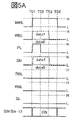
- FIG. 5A is a timing chart showing an example of a method of driving a semiconductor device.
- 5B to 5E are circuit diagrams showing an example of a method of driving a semiconductor device.
- FIG. 6 is a timing chart showing an example of a method of driving a semiconductor device.
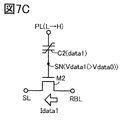
- FIG. 7A to 7C are circuit diagrams showing an example of a method of driving a semiconductor device.
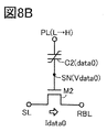
- FIG. 8A is a timing chart showing an example of a method of driving a semiconductor device.
- 8B and 8C are circuit diagrams showing an example of a method of driving a semiconductor device.
- 9A and 9B are circuit diagrams showing a configuration example of a memory cell.
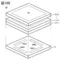
- 10A and 10B are perspective views showing a configuration example of a semiconductor device.
- FIG. 11 is a perspective view showing a configuration example of the semiconductor device.
- FIG. 12 is a diagram showing an example of the layout of the semiconductor device.
- FIG. 13 is a schematic cross-sectional view showing a configuration example of a semiconductor device.
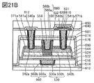
- 14A to 14C are schematic cross-sectional views showing a configuration example of a transistor.
- FIG. 15 is a schematic cross-sectional view showing a configuration example of a semiconductor device.
- 16A and 16B are schematic cross-sectional views showing a configuration example of a transistor.
- FIG. 17 is a schematic cross-sectional view showing a configuration example of a transistor.
- 18A to 18C are schematic cross-sectional views showing a configuration example of a transistor.
- FIG. 19 is a schematic cross-sectional view showing a configuration example of a transistor.
- 20A and 20B are schematic cross-sectional views showing a configuration example of a transistor.
- 21A and 21B are schematic cross-sectional views showing a configuration example of a transistor.
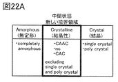
- FIG. 22A is a diagram illustrating the classification of the crystal structure of IGZO.
- FIG. 22B is a diagram illustrating an XRD spectrum of crystalline IGZO.
- FIG. 22C is a diagram illustrating a microelectron diffraction pattern of crystalline IGZO.
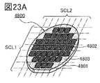
- FIG. 23A is a perspective view showing an example of a semiconductor wafer.
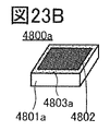
- FIG. 23B is a perspective view showing an example of the chip.
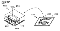
- 23C and 23D are perspective views showing an example of an electronic component.
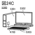
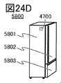
- 24A to 24J are views showing an example of an electronic device.
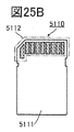
- 25A to 25E are diagrams showing an example of an electronic device.
- 26A to 26C are diagrams showing an example of an electronic device.
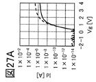
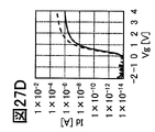
- 27A to 27F are diagrams showing the measurement results of the Id-Vg characteristics according to the examples.
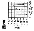
- FIG. 28A to 28F are views showing the results of the drain withstand voltage test according to the embodiment.
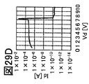
- 29A to 29F are views showing the results of the drain withstand voltage test according to the embodiment.
- FIG. 30A is a circuit diagram illustrating an outline of the off-current measurement TEG.
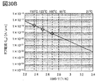
- FIG. 30B is a graph showing the temperature dependence of the leak current.
- FIG. 31A is a schematic diagram showing the structure of the prototype transistor. 31B and 31C are cross-sectional STEM images of the prototype transistor.
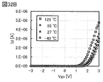
- 32 FIGS. 32A and 32B are top gate voltage-drain current characteristics of the prototype transistor.
- FIG. 33 is a diagram showing the current gain of the maximum gain in the prototype transistor.
- the ordinal numbers “first”, “second”, and “third” are added to avoid confusion of the components. Therefore, the number of components is not limited. Moreover, the order of the components is not limited. Further, for example, the component referred to in “first” in one of the embodiments of the present specification and the like is assumed to be another embodiment or the component referred to in “second” in the scope of claims. It is possible. Further, for example, the component referred to in “first” in one of the embodiments of the present specification and the like may be omitted in another embodiment or in the scope of claims.
- a metal oxide is a metal oxide in a broad sense. Metal oxides are classified into oxide insulators, oxide conductors (including transparent oxide conductors), oxide semiconductors (also referred to as Oxide Semiconductor or simply OS) and the like. For example, when a metal oxide is used for the active layer of a transistor, the metal oxide may be referred to as an oxide semiconductor. That is, when a metal oxide can form a channel forming region of a transistor having at least one of an amplification action, a rectifying action, and a switching action, the metal oxide can be referred to as a metal oxide semiconductor. can. Further, in the case of describing as an OS FET or an OS transistor, it can be paraphrased as a transistor having a metal oxide or an oxide semiconductor.
- One aspect of the present invention relates to a semiconductor device having a cell.
- the cell has a first transistor, a second transistor, and a capacitance.
- One of the source or drain of the first transistor is electrically connected to the gate of the second transistor.
- the gate of the second transistor is electrically connected to one of the electrodes of the capacitance.
- the cell can be called a memory cell, and the semiconductor device can be called a storage device.
- the capacitance is configured to provide a ferroelectric layer between a pair of electrodes.
- the data written in the memory cell can be held by the polarization of the ferroelectric layer.
- one electrode of the capacitance is electrically suspended and the potential of the other electrode of the capacitance is changed.
- the fluctuation range of the potential of one electrode of the capacitance can be determined by the ratio of the capacitance value of the capacitance to the parasitic capacitance of the node to which one electrode of the capacitance is electrically connected.
- the amount of polarization of the ferroelectric layer is different.
- the capacity value of the capacity is different. Therefore, if the potential of the other electrode of the capacitance is changed, the potential of one electrode of the capacitance can be changed according to the data held in the memory cell. Based on this difference, data can be read from the memory cell.
- the data to be read from the memory cell is different, if the potentials of one electrode of the capacitance are significantly different, the data can be read with high accuracy.
- the semiconductor device of one aspect of the present invention when reading data from a memory cell, it is possible to control the parasitic capacitance of the node to which one electrode of the capacitance is electrically connected. As a result, data can be read from the memory cell with high accuracy.
- FIG. 1 is a block diagram showing a configuration example of a semiconductor device 10 which is a semiconductor device according to an aspect of the present invention.
- the semiconductor device 10 includes a storage unit MU, a drive circuit WWD, a drive circuit RWD, a drive circuit WBD, and a drive circuit RBD.
- FIG. 2 is a circuit diagram showing a configuration example of the storage unit MU. Note that FIG. 2 also shows the drive circuit WBD.
- the storage unit MU has a memory cell array MCA ⁇ 1> to a memory cell array MCA ⁇ k> (k is an integer of 1 or more), and a switch array SWA ⁇ 0> to a switch array SWA ⁇ k-1>.
- the switch array SWA ⁇ 0> is provided between the drive circuit WBD and the memory cell array MCA ⁇ 1>.
- the switch array SWA ⁇ 1> is provided between the memory cell array MCA ⁇ 1> and the memory cell array MCA ⁇ 2>.
- the switch array SWA ⁇ k-1> is provided between the memory cell array MCA ⁇ k-1> and the memory cell array MCA ⁇ k>. That is, the storage unit MU is alternately provided with the switch array SWA and the memory cell array MCA. Note that FIG. 2 does not show the memory cell array MCA ⁇ k-1>.
- Switch SWs are arranged in the switch array SWA. Specifically, for example, a plurality of switch SW ⁇ 0> are arranged in the switch array SWA ⁇ 0>, a plurality of switch SW ⁇ 1> are arranged in the switch array SWA ⁇ 1>, and a plurality of switch SW ⁇ 1> are arranged in the switch array SWA ⁇ 2>. A plurality of switches SW ⁇ 2> are arranged, and a plurality of switches SW ⁇ k-1> are arranged in the switch array SWA ⁇ k-1>.
- the switch SW can be, for example, a transistor.
- one terminal of the switch SW ⁇ 0> is electrically connected to the drive circuit WBD, and the other terminal of the switch SW ⁇ 0> is electrically connected to the memory cell array MCA ⁇ 1>.
- one terminal of the switch SW ⁇ 1> is electrically connected to the memory cell array MCA ⁇ 1>, and the other terminal of the switch SW ⁇ 1> is electrically connected to the memory cell array MCA ⁇ 2>. ..
- one terminal of the switch SW ⁇ k-1> is electrically connected to the memory cell array MCA ⁇ k-1>, and the other terminal of the switch SW ⁇ k-1> is connected to the memory cell array MCA ⁇ k>. It is electrically connected. That is, the drive circuit WBD is electrically connected to the memory cell array MCA via the switch SW. Further, the memory cell array MCA are electrically connected to each other via the switch SW.
- the drive circuit WBD is electrically connected to the memory cell array MCA ⁇ 1> to the memory cell array MCA ⁇ k> by the wiring WBL via the switch SW.
- the drive circuit WBD is electrically connected to the memory cell array MCA ⁇ 1> via the switch SW ⁇ 0>, and is connected to the memory cell array MCA ⁇ 2> via the switch SW ⁇ 0> and the switch SW ⁇ 1>. It is electrically connected and is electrically connected to the memory cell array MCA ⁇ k> via the switch SW ⁇ 0> to the switch SW ⁇ k-1>.
- the wiring WBL has a capacitance C1 which is a parasitic capacitance.
- the capacitance C1 of the wiring WBL between the other terminal of the switch SW ⁇ 0> and one terminal of the switch SW ⁇ 1> is defined as the capacitance C1 ⁇ 1>.
- the capacitance C1 of the wiring WBL between the other terminal of the switch SW ⁇ 1> and one terminal of the switch SW ⁇ 2> is defined as the capacitance C1 ⁇ 2>.
- the capacitance C1 of the wiring WBL between the other terminal of the switch SW ⁇ k-2> and one terminal of the switch SW ⁇ k-1> is defined as the capacitance C1 ⁇ k-1>.
- the parasitic capacitance of the wiring WBL from the other terminal of the switch SW ⁇ k-1> to the memory cell array MCA ⁇ k> is defined as the capacitance C1 ⁇ k>.
- FIG. 2 does not show the switch array SWA ⁇ k-2> and the switch SW ⁇ k-2>.
- the capacitance values of the capacitances C1 ⁇ 1> to C1 ⁇ k> are the same. Can be regarded.
- the parasitic capacitance is shown by a broken line. The same description may be made in other figures.
- FIG. 3 is a block diagram showing a configuration example of the semiconductor device 10.
- the storage unit MU has the configuration shown in FIG. 2, and a specific configuration example of the memory cell array MCA is shown.
- Memory cells MC are arranged in a matrix in the memory array MCA.
- the drive circuit WWD is electrically connected to the memory cell MC by the wiring WWL.
- the drive circuit RWD is electrically connected to the memory cell MC by the wiring RWL.
- the drive circuit WWD and the drive circuit RWD are electrically connected to the memory cell MC by the wiring PL.
- the drive circuit RBD is electrically connected to the memory cell MC by the wiring RBL.
- the drive circuit WBD is electrically connected to the memory cell MC by the wiring WBL via the switch SW.
- the memory cells MC in the same row can be electrically connected by the same wiring WWL, wiring PL, and wiring RWL.
- the memory cells MC in the same row can be electrically connected by the same wiring WBL and wiring RBL.
- the switch array SWA may be provided with switch SWs for each row of memory cell MCs.
- the drive circuit WWD has a function of generating a signal for controlling the selection of the memory cell MC to which the data is written.
- the drive circuit WWD has a function of generating a signal to be given to the wiring WWL, and also has a function of generating a signal to be given to the wiring PL.
- the drive circuit WWD can generate a signal for desired selection control by using a decoder circuit, a shift register circuit, or the like.
- the drive circuit RWD has a function of generating a signal for controlling the selection of the memory cell MC from which the data is read.
- the drive circuit RWD has a function of generating a signal to be given to the wiring RWL, and also has a function of generating a signal to be given to the wiring PL.
- the drive circuit RWD can generate a signal for desired selection control by using a decoder circuit, a shift register circuit, or the like.
- the signal given to the wiring PL can be generated by the drive circuit WWD when the data is written to the memory cell MC.
- the drive circuit RWD when reading data from the memory cell MC, the drive circuit RWD can be generated.
- the drive circuit WBD has a function of outputting a data signal to be written to the memory cell MC.
- the drive circuit WBD has a function of outputting a data signal given to the wiring WBL.
- the drive circuit WBD has a decoder circuit and a plurality of latch circuits.
- the drive circuit WBD has a function of outputting a data signal held in the latch circuit at a timing of writing data to the memory cell MC.
- the drive circuit RBD has a function of reading data from the memory cell MC. Specifically, the drive circuit RBD has a function of determining the data read from the memory cell MC based on the potential output from the memory cell MC when the data is read from the memory cell MC. For example, when binary data is read from the memory cell MC, it is determined whether the value of the data read from the memory cell MC is "0" or "1" based on the potential output from the memory cell MC. Has a function. The drive circuit RBD has a function of determining data read from the memory cell MC, for example, by comparing the magnitude relationship between the potential of the wiring RBL and the reference potential.
- the drive circuit RBD has a function of outputting a potential representing data read from the memory cell MC to, for example, the outside of the semiconductor device 10.
- the drive circuit RBD can generate a desired potential to be output to the outside based on the potential output from the memory cell MC by using an amplifier circuit, a comparison circuit, or the like.
- the drive circuit RBD may have a precharge circuit. In this case, the drive circuit RBD can output the precharge potential to the wiring RBL.
- the wiring WWL can be referred to as a write word line or simply a word line
- the drive circuit WWD can be referred to as a write word line drive circuit or simply a word line drive circuit.
- the wiring RWL can be referred to as a read word line or simply a word line
- the drive circuit RWD can be referred to as a read word line drive circuit or simply a word line drive circuit.
- the wiring PL can be called a plate wire.
- the wiring WBL can be referred to as a write bit line or simply a bit line
- the drive circuit WBD can be referred to as a write bit line drive circuit or simply a bit line drive circuit.
- the wiring RBL can be referred to as a read bit line or simply a bit line
- the drive circuit RBD can be referred to as a read bit line drive circuit or simply a bit line drive circuit.
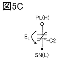
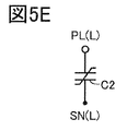
- FIG. 4 is a circuit diagram showing a configuration example of the memory cell MC.
- the memory cell MC has a transistor M1, a transistor M2, a transistor M3, and a capacitance C2.
- the capacitance C2 is a ferroelectric capacitance provided with a ferroelectric layer between a pair of electrodes.
- the capacitance C2, which is a ferroelectric capacitance provided with a ferroelectric layer, is indicated by a circuit symbol different from that of a capacitance not provided with a ferroelectric layer.
- each transistor will be described as an n-channel type transistor.
- the transistor M1 when the transistor M1 is an n-channel type transistor and the wiring WWL is set to a high potential (also referred to as H level potential or H level), the transistor M1 can be turned on. Further, when the wiring WWL is set to a low potential (also referred to as L level potential or L level), the transistor M1 can be turned off. The same applies to the transistor M3.
- the following description can be applied even if a part or all of the transistors of the memory cell MC are p-channel transistors by appropriately reversing the magnitude relationship of the potentials.
- One of the source and drain of the transistor M1 is electrically connected to the gate of the transistor M2.
- the gate of the transistor M2 is electrically connected to one electrode of the capacitance C2.
- One of the source or drain of the transistor M2 is electrically connected to one of the source or drain of the transistor M3.
- a node in which one of the source or drain of the transistor M1, the gate of the transistor M2, and one electrode of the capacitance C2 is electrically connected is referred to as a node SN.
- the other of the source or drain of the transistor M1 is electrically connected to a terminal that transmits a signal of the wiring WBL.
- the gate of the transistor M1 is electrically connected to a terminal that transmits a signal of the wiring WWL.
- the other of the source or drain of the transistor M2 is electrically connected to the terminal that transmits the signal of the wiring SL.
- the other of the source or drain of the transistor M3 is electrically connected to a terminal that transmits a signal of the wiring RBL.
- the gate of the transistor M3 is electrically connected to a terminal that transmits a signal of the wiring RWL.
- the other electrode of the capacitance C2 is electrically connected to a terminal that transmits a signal of the wiring PL.
- the wiring SL is wiring to which a constant potential for reading data from the memory cell MC is given.
- a current can be passed between the wiring RBL and the wiring SL according to the data held in the memory cell MC.
- transistors M1 to M3 a transistor having silicon in the channel forming region (hereinafter referred to as Si transistor) and / or a transistor having an oxide semiconductor in the channel forming region (hereinafter referred to as OS transistor) can be used.
- Si transistor silicon in the channel forming region
- OS transistor oxide semiconductor in the channel forming region
- the silicon used in the channel forming region of the Si transistor may be, for example, amorphous silicon (sometimes referred to as hydrided amorphous silicon), microcrystalline silicon, polycrystalline silicon, single crystal silicon, or the like.
- a transistor containing Ge or the like in the channel forming region, or a compound semiconductor such as ZnSe, CdS, GaAs, InP, GaN, or SiGe is included in the channel forming region.
- Transistors included, transistors in which carbon nanotubes are contained in the channel forming region, transistors in which organic semiconductors are contained in the channel forming region, and the like can be used.
- the OS transistor can be freely arranged by stacking it on a circuit using a Si transistor or the like, integration can be easily performed. Further, since the OS transistor can be manufactured by using the same manufacturing apparatus as the Si transistor, it can be manufactured at low cost.
- the OS transistor has better electrical characteristics than the Si transistor in a high temperature environment. Specifically, since the ratio of the on current to the off current is large even at a high temperature such as 100 ° C. or higher and 200 ° C. or lower, preferably 125 ° C. or higher and 150 ° C. or lower, good switching operation can be performed.
- FIG. 4B is a schematic diagram showing a configuration example of the capacitance C2.
- the capacitance C2 includes a ferroelectric layer FE between the electrode UE and the electrode LE.
- the capacitance C2 provided with such a ferroelectric layer may be referred to as a ferroelectric capacitance or a ferroelectric capacitor.
- the capacitance C2 When a voltage (electric field or electric field) is applied between the electrode UE and the electrode LE, the capacitance C2 provided with the ferroelectric layer polarizes the ferroelectric layer FE according to the application direction and amount of the voltage. The direction and the amount of polarization change. A signal (data) is held (written) between the electrode UE and the electrode LE by utilizing the change in the polarization state of the ferroelectric layer FE. In the capacitance C2, the polarization remains in the ferroelectric layer FE even if the voltage between the electrode UE and the electrode LE is set to zero. In order to rewrite the polarization, a voltage for reversing the polarization (polarization inversion voltage) is applied.
- polarization inversion voltage polarization inversion voltage
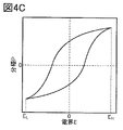
- FIG. 4C is a graph showing the magnitude of polarization of the ferroelectric layer FE according to the electric field applied to the ferroelectric layer FE.
- the horizontal axis shows the electric field E applied to the ferroelectric layer FE.
- the vertical axis shows the polarization P of the ferroelectric layer FE.
- the polarization of the ferroelectric layer FE increases.
- the electric field E H is applied to the ferroelectric layer FE and then the electric field applied to the ferroelectric layer FE is lowered, the negative charge is biased to one electrode side of the capacitance C2 and the positive charge is the other of the capacitance C2. Since it is biased toward the electrode side of, positive polarization remains when the electric field becomes zero.
- the electric field EL applied to the ferroelectric layer FE is increased and then the electric field applied to the ferroelectric layer FE is increased, the positive charge is biased to one electrode side of the capacitance C2 and the negative charge is biased to the other electrode side of the capacitance C2.
- the voltage for applying the electric field E H and the electric field EL to the ferroelectric layer FE can be said to be a polarization inversion voltage.
- the polarization inversion voltage By applying the polarization inversion voltage to the capacitance C2, data can be written to the memory cell MC.
- Examples of the material having a ferroelectricity that can be used for the ferroelectric layer FE include hafnium oxide, zirconium oxide, and metal oxides such as HfZrOX ( X is a real number larger than 0). .. Further, as a material capable of having strong dielectric property, hafnium oxide and element J1 (the element J1 here is zirconium (Zr), silicon (Si), aluminum (Al), gadolinium (Gd), yttrium (Y)). , One or more selected from lanthanum (La), yttrium (Sr) and the like).
- the ratio of the number of atoms of the hafnium atom and the element J1 can be appropriately set, and for example, the number of atoms of the hafnium atom and the element J1 may be 1: 1 or in the vicinity thereof.
- zirconium oxide is added to the element J2 (the element J2 here is hafnium (Hf), silicon (Si), aluminum (Al), gadolinium (Gd), yttrium (Y)). , One or more selected from lanthanum (La), strontium (Sr) and the like, and the like.
- the ratio of the number of atoms of the zirconium atom to the element J2 can be appropriately set, and for example, the number of atoms of the zirconium atom to the element J2 may be 1: 1 or close to it.
- materials capable of having strong dielectric property lead titanate (PbTiO X ), barium titanate strontium (BST), strontium titanate, lead zirconate titanate (PZT), strontium bismuthate tantanate (SBT), A piezoelectric ceramic having a perovskite structure such as bismuth ferrite (BFO) or barium titanate may be used.
- aluminum nitride scandium Al 1-a Sc a N b (a is a real number larger than 0 and smaller than 0.5, and b is a value of 1 or its vicinity).
- Al-Ga-Sc nitrides Al-Ga-Sc nitrides
- metal nitrides such as Ga-Sc nitrides.
- the material having a ferroelectricity include a metal nitride having an element M1, an element M2, and nitrogen.
- the element M1 is one or a plurality selected from aluminum (Al), gallium (Ga), indium (In) and the like.
- the element M2 is boron (B), scandium (Sc), yttrium (Y), lanthanum (La), cerium (Ce), neodymium (Nd), europium (Eu), titanium (Ti), zirconium (Zr). , Hafnium (Hf), vanadium (V), niobium (Nb), tantalum (Ta), chromium (Cr) and the like.
- the ratio of the number of atoms of the element M1 to the number of atoms of the element M2 can be appropriately set. Further, the metal oxide having the element M1 and nitrogen may have ferroelectricity even if the element M2 is not contained.
- Examples of the material having a ferroelectricity include a material in which the element M3 is added to the metal nitride.
- the element M3 is one or a plurality selected from magnesium (Mg), calcium (Ca), strontium (Sr), zinc (Zn), cadmium (Cd) and the like.
- Mg magnesium
- Ca calcium
- Zn zinc
- Cd cadmium
- the ratio of the number of atoms of the element M1, the number of atoms of the element M2, and the number of atoms of the element M3 can be appropriately set.
- the metal nitride contains at least a group 13 element and a group 15 element, nitrogen, the metal nitride is a strong dielectric of group 3-5 or a group 3 nitride. It may be called a strong dielectric or the like.
- Examples of the material having a ferroelectricity include a perovskite-type oxynitride such as SrTaO 2N or BaTaO 2N, or GaFeO 3 having a ⁇ -alumina type structure.
- metal oxides and metal nitrides have been exemplified, but the present invention is not limited thereto.
- a metal oxide nitride obtained by adding nitrogen to the above-mentioned metal oxide a metal nitride oxide obtained by adding oxygen to the above-mentioned metal nitride, or the like may be used.
- the material capable of having ferroelectricity for example, a mixture or compound composed of a plurality of materials selected from the materials listed above can be used.
- the ferroelectric layer FE can have a laminated structure composed of a plurality of materials selected from the materials listed above.
- the crystal structure (characteristics) of the materials and the like listed above may change not only by the film forming conditions but also by various processes and the like, the materials exhibiting ferroelectricity are strongly used in the present specification and the like. Not only is it called a dielectric, but it is also called a material that can have ferroelectricity.
- the ferroelectric substance includes not only a material exhibiting ferroelectricity but also a material capable of having ferroelectricity.
- the film thickness of the ferroelectric layer FE can be 100 nm or less, preferably 50 nm or less, more preferably 20 nm or less, still more preferably 10 nm or less (typically 2 nm or more and 9 nm or less).
- the film thickness is preferably 8 nm or more and 12 nm or less.
- the capacitance C2 can be combined with a semiconductor element such as a miniaturized transistor to form a semiconductor device.
- a layered material capable of having ferroelectricity may be referred to as a ferroelectric layer, a metal oxide film, or a metal nitride film.
- a ferroelectric device in the present specification and the like.
- HfZrOX When used as a material capable of having ferroelectricity, it is preferable to form a film by using an atomic layer deposition (ALD) method, particularly a thermal ALD method. Further, when a material capable of having ferroelectricity is formed by using the thermal ALD method, it is preferable to use a material containing no hydrocarbon (also referred to as Hydro Carbon, HC) as a precursor. When one or both of hydrogen and carbon are contained in the material which may have a ferroelectricity, the crystallization of the material which may have a ferroelectricity may be inhibited.
- ALD atomic layer deposition
- HC Hydro Carbon
- a precursor containing no hydrocarbon a chlorine-based material can be mentioned.
- HfZrO x hafnium oxide and zirconium oxide
- HfCl 4 and / or ZrCl 4 may be used as the precursor.
- high-purity intrinsicity is achieved by thoroughly eliminating at least one of impurities, here hydrogen, hydrocarbon, and carbon in the film. It is possible to form a film having a strong ferroelectricity. It should be noted that the film having high-purity intrinsic ferroelectricity and the high-purity intrinsic oxide semiconductor shown in the embodiment described later have very high consistency in the manufacturing process. Therefore, it is possible to provide a method for manufacturing a semiconductor device having high productivity.
- HfZrOX is used as a material capable of having ferroelectricity
- the oxidizing agent of the thermal ALD method is not limited to this.
- the oxidizing agent in the thermal ALD method may contain one or more selected from O 2 , O 3 , N 2 O, NO 2 , H 2 O, and H 2 O 2 .
- the crystal structure of the material that can have ferroelectricity is not particularly limited.
- the crystal structure of the material capable of having strong dielectric property may be one or more selected from cubic, tetragonal, orthorhombic, and monoclinic.
- a material capable of having ferroelectricity it is preferable to have an orthorhombic crystal structure because ferroelectricity is exhibited.
- a composite structure having an amorphous structure and a crystal structure may be used as a material capable of having ferroelectricity.
- the writing of data to the memory cell MC is performed according to the direction of the electric field on the ferroelectric layer of the capacitance C2, which is given by the potential of the node SN and the potential of the wiring PL.
- data is written to the memory cell MC by applying a polarization inversion voltage to the capacitance C2.
- the ferroelectric layer having the capacitance C2 can take different polarization states depending on the data written in the memory cell MC. Therefore, the data written in the memory cell MC can be held by the polarization state of the ferroelectric layer possessed by the capacitance C2.
- the difference in the polarization state is maintained even when the electric field to the capacitance C2 is 0, for example. Therefore, for example, even if the electric field to the capacitance C2 is set to 0, the data can be continuously held in the memory cell MC.
- the data read from the memory cell MC is performed by utilizing the capacitive coupling in the capacitance C2 when the potential of the wiring PL is changed.
- the node SN is electrically suspended, so that capacitive coupling occurs in the capacitance C2. Therefore, the potential of the node SN changes according to the change of the potential of the wiring PL.
- the change in the potential of the node SN differs depending on the capacitance value of the capacitance C2, and the capacitance value of the capacitance C2 differs depending on the polarization state of the ferroelectric layer possessed by the capacitance C2. Therefore, the potential of the gate of the transistor M2 can be changed according to the retained data.
- the potential of the gate of the transistor M2 is different, the amount of current flowing between the source and the drain of the transistor M2 is different. As a result, the potentials of the wiring RBLs are different. Data can be read from the memory cell MC due to the difference in the potential of the wiring RBL.
- FIG. 5A is a timing chart showing the operation of writing data in the memory cell MC.
- FIG. 5A shows the potentials of the wiring WWL, the wiring WBL, the wiring PL, the node SN, the wiring RBL, the wiring RWL, and the wiring SL. Further, FIG. 5A shows the states of the switch SW ⁇ 0> to the switch SW ⁇ k-1>. Further, in FIG. 5A, "data1" and “data0" are shown as data to be written to the memory cell MC. "Data1” is shown as a high-potential signal, and “data0” is shown as a low-potential signal.
- the potential of the wiring WWL, the potential of the wiring WBL, the potential of the wiring PL, the potential of the node SN, the potential of the wiring RBL, the potential of the wiring RWL, and the potential of the wiring SL are low potentials.
- the switch SW ⁇ 0> to the switch SW ⁇ k-1> are set to the ON state (ON).
- the drive circuit WBD gives the wiring WBL the potential of the signal corresponding to the data “data1” or “data0” to be written to the memory cell MC.
- the potential of the wiring WWL is set to a high potential.
- the potential of the wiring WBL is given to the node SN.
- the potential of the wiring PL is set to a high potential.
- the potential shown in FIG. 5B is applied to the electrode of the capacitance C2.
- the electrodes of the capacitance C2 are both at high potential and equipotential, no voltage exceeding the inverting polarization voltage is applied and no electric field is generated in the ferroelectric layer.
- the potential shown in FIG. 5C is applied to the electrode of the capacitance C2.
- the transistors M1 to M3 are preferably transistors having excellent resistance (withstand voltage) to a high voltage.
- the transistors M1 to M3 are preferably composed of OS transistors.
- the OS transistor has a characteristic of having excellent withstand voltage as compared with the Si transistor.
- the potential of the wiring PL is set to a low potential.
- the potential shown in FIG. 5D is applied to the electrode of the capacitance C2.
- an inverting polarization voltage opposite to the inverting polarization voltage in FIG. 5C is applied to the capacitance C2, and an electric field EH is generated in the ferroelectric layer.
- the polarization state corresponding to "data1" is written in the capacitance C2.
- the potential shown in FIG. 5E is applied to the electrode of the capacitance C2.
- the electrodes of the capacitance C2 are both at low potential and equipotential, no voltage exceeding the inverting polarization voltage is applied and no electric field is generated in the ferroelectric layer.
- the potential of the wiring WBL is set to a low potential.
- the potential of the node SN becomes low.
- the potential of the wiring PL is also low, a voltage exceeding the inverting polarization voltage is not applied to the ferroelectric layer having the capacitance C2. Therefore, the state of polarization of the ferroelectric layer is maintained. Therefore, the data written in the memory cell MC at time T01 to time T03 is retained.
- the potential of the wiring WWL is set to a low potential, and the switch SW ⁇ 0> to the switch SW ⁇ k-1> are turned off. As a result, the operation of writing data to the memory cell MC is completed.
- FIG. 6 is a timing chart showing the operation of reading data in the memory cell MC.
- FIG. 6 shows the potentials of the wiring WWL, the wiring WBL, the wiring PL, the node SN, the wiring RBL, the wiring RWL, and the wiring SL, as in FIG. 5A. Further, the states of the switch SW ⁇ 0> to the switch SW ⁇ k-1> are shown. Further, “data1” and “data0” are shown as data to be written to the memory cell MC. In FIG. 6, "data1" and “data0” correspond to the data held as the polarization state of the ferroelectric layer having the capacitance C2 in the data writing operation.
- the potential of the wiring WWL, the potential of the wiring WBL, the potential of the wiring PL, the potential of the node SN, the potential of the wiring RBL, the potential of the wiring RWL, and the potential of the wiring SL are low potentials.
- the switch SW ⁇ 0> is turned off.
- the electrical connection between the drive circuit WBD and the memory cell MC is cut off, and for example, the signal generated by the drive circuit WBD is not given to the memory cell MC.
- the potential of the wiring WWL is set to a high potential.
- the transistor M1 is turned on, and the node SN and the wiring WBL are conducted.
- the node SN is electrically suspended even if the node SN and the wiring WBL are electrically connected.
- the potential of the wiring RBL is precharged to, for example, a high potential.
- the switch SW ⁇ 1> to the switch SW ⁇ k-1> are set to an ON state or an OFF state (ON or OFF), respectively. The method of determining the switch SW to be turned on will be described later.
- the potential of the wiring PL is set to a high potential.
- the node SN is electrically in a floating state. Therefore, the potential of the node SN fluctuates depending on the capacitance C2 and the capacitive coupling in the node SN.
- FIG. 7A is a circuit diagram in which a parasitic capacitance and the like are added to the memory cell MC shown in FIG. 4A.
- the node SN has a capacitance C3 which is a parasitic capacitance caused by the gate capacitance of the transistor M2 and the like.
- the wiring WBL has a capacitance C1 which is a parasitic capacitance.
- the node SN and the wiring WBL are in a conductive state.
- the fluctuation width ⁇ V SN of the potential of the node SN due to the fluctuation of the potential of the wiring PL is the capacitance value C FE of the capacitance C2, the capacitance value CS of the capacitance C3 which is a parasitic capacitance, and the wiring WBL. It is determined by the capacitance value C WBL caused by the capacitance C1 which is a parasitic capacitance, and if the fluctuation range of the potential of the wiring PL is ⁇ VPL, the ⁇ V SN can be expressed by the equation (1).
- the capacitance value CFE of the capacitance C2 is determined by the polarization state of the ferroelectric layer possessed by the capacitance C2. This polarization state differs depending on whether the data held in the memory cell MC is "data1" or "data0". Therefore, the fluctuation width ⁇ V SN of the potential of the node SN can be made different depending on the data held in the memory cell, and thus the potential V SN of the node SN can be made different.
- the potential of the wiring RWL is set to a high potential.
- the transistor M3 is turned on, and a current corresponding to the potential of the node SN flows between the drain and the source of the transistor M2.
- FIG. 7B shows the potential of the node SN when the potential of the wiring PL is changed from the low potential to the high potential when “data0” is held in the memory cell MC, and flows between the drain and the source of the transistor M2. It is a figure which shows the electric potential. In the case shown in FIG. 7B, it is assumed that the potential of the node SN is the potential Vdata0, and the current flowing between the drain and the source of the transistor M2 is the current Idata0.
- FIG. 7C shows the potential of the node SN when the potential of the wiring PL is changed from the low potential to the high potential when “data1” is held in the memory cell MC, and flows between the drain and the source of the transistor M2. It is a figure which shows the electric potential. In the case shown in FIG. 7C, it is assumed that the potential of the node SN is the potential Vdata1 and the current flowing between the drain and the source of the transistor M2 is the current Idata1. It is assumed that the current Idata1 is larger than the current Idata0.
- the current Idata1 is larger than the current Idata0. Therefore, assuming that the potential of the wiring RBL is higher than the potential of the wiring SL, the potential of the wiring RBL when "data1" is held in the memory cell MC is the case where "data0" is held in the memory cell MC. It becomes lower than the potential of the wiring RBL. Therefore, data can be read from the memory cell MC based on the potential of the wiring RBL.
- the capacity value of the capacity C2 when the data held in the memory cell MC is “data1” is set as the capacity value CFE1
- the capacity when the data held in the memory cell MC is “data0”.
- the capacity value of C2 be the capacity value C FE0 .
- ⁇ Vdata can be expressed by the equation (2).
- the value Cmax of "C s + C WBL " when ⁇ Vdata is maximum is a value at which the value of the derivative obtained by partially differentiating the equation (2) with "C s + C WBL " becomes 0, and the equation It can be represented by (3).
- ⁇ Vdata can be increased by adjusting the value of C WBL so that “C s + C WBL ” becomes ⁇ (C FE1 ⁇ C FE0 ).
- the capacitance value C WBL can be controlled by controlling the on / off of the switch SW. For example, when all the switches SW ⁇ 1> to the switch SW ⁇ k-1> are turned off, one capacitance C1 is electrically connected to the node SN. On the other hand, for example, if one of the switch SW ⁇ 1> to the switch SW ⁇ k-1>, which is electrically connected to the memory cell for reading data, is turned on, the node SN has two capacities. C1 will be electrically connected. Therefore, the capacitance value C WBL can be increased as compared with the case where all the switches SW ⁇ 1> to the switch SW ⁇ k-1> are turned off. By increasing the number of switch SWs to be turned on, the capacitance value C WBL can be further increased.
- the capacitance value C FE1 and the capacitance value C FE0 change, it is preferable to adjust the number of switch SWs to be turned on accordingly.
- the capacitance value C FE1 and the capacitance value C FE0 may change due to fatigue deterioration of the ferroelectric layer of the capacitance C2.
- the semiconductor device 10 can be a highly reliable semiconductor device.
- the potential of the wiring PL and the potential of the wiring RWL are set to be low potentials.
- the potential of the wiring WWL is set to a low potential.
- the semiconductor device of one aspect of the present invention has a plurality of memory cell array MCA, and a switch array SWA is provided between the memory cell array MCA.
- the write bit line drive circuit is electrically connected to each of the plurality of memory cell array MCA by the write bit line via the switch SW provided in the switch array SWA.
- the semiconductor device of one aspect of the present invention when reading data from the memory cell MC provided in the memory cell array MCA, a high potential is applied to the wiring WWL which is a write word line, and the transistor M1 is turned on. Further, the capacity value C FE1 of the capacity C2 when the data held in the memory cell MC is “data1” and the capacity value of the capacity C2 when the data held in the memory cell MC is “data0”. The on / off of the switch SW is controlled based on C FE0 . Thereby, the difference between the potential of the wiring RBL when reading “data0” from the memory cell MC and the potential of the wiring RBL when reading “data1” from the memory cell MC can be increased. Therefore, data can be read out from the memory cell MC with high accuracy.
- FIG. 8A is a timing chart showing the operation of reading data in the memory cell MC, and is a modification of the operation method shown in FIG.
- the potential of the wiring SL is set to a high potential. Further, at time T11 to time T12, the potential of the wiring RBL is precharged to a low potential.
- FIGS. 8B and 8C are diagrams showing the current flowing between the drain and the source of the transistor M2 at time T13 to time T14, and are modified examples of FIGS. 7B and 7C, respectively.
- the current Idata0 corresponding to the potential Vdata0 or the current Idata1 corresponding to the potential Vdata1 is wired at time T13 to time T14. It flows from SL toward wiring RBL.
- FIG. 9A and 9B are circuit diagrams showing a configuration example of the memory cell MC, and are modified examples of the memory cell MC shown in FIG. 4A.
- the memory cell MCa shown in FIG. 9A is different from the memory cell MC shown in FIG. 4A in that the transistors M1 to M3 have a back gate electrode.
- a back gate voltage VBG is applied to the back gates of the transistors M1 to M3.
- the on-current of each transistor can be increased.
- the memory cell MCb shown in FIG. 9B differs from the memory cell MC shown in FIG. 4A in that the transistor M3 is omitted and the wiring RWL is electrically connected to the back gate of the transistor M2.
- the threshold voltage of the transistor M2 can be controlled by the selection signal given to the wiring RWL. Thereby, it is possible to control whether or not a current flows between the wiring RBL and the wiring SL.
- FIG. 10A is a perspective view showing a configuration example of the semiconductor device 10.
- the semiconductor device 10 shown in FIG. 10A has a layer 11 and a layer 13.
- the layer 11 and the layer 13 are laminated so as to have a region overlapping with each other.
- the layer 11 and the layer 13 are shown separately in order to make the configuration of the semiconductor device 10 easy to understand. The same description is made in other figures.
- the layer 11 may be provided with a drive circuit WWD, a drive circuit RWD, a drive circuit WBD, and a drive circuit RBD, and the layer 13 may be provided with a storage unit MU. Therefore, the semiconductor device 10 can be designed so as to have a region where the storage unit MU and the drive circuit overlap.
- the drive circuit and the memory cell provided in the storage unit MU can be configured by transistors having different electrical characteristics.
- the drive circuit can be configured by a Si transistor
- the memory cell provided in the storage unit MU can be configured by an OS transistor. Therefore, the degree of freedom in designing the semiconductor device 10 can be increased.
- FIG. 10B is a perspective view showing a configuration example of the semiconductor device 10, and is a modification of the semiconductor device 10 shown in FIG. 10A.
- the semiconductor device 10 shown in FIG. 10B is provided with a plurality of layers 13.
- FIG. 10B shows an example in which the layer 13 is provided with k layers.
- the layer 13 ⁇ 1> is provided with a memory cell array MCA ⁇ 1> and a switch array SWA ⁇ 0>.
- the layer 13 ⁇ 2> is provided with a memory cell array MCA ⁇ 2> and a switch array SWA ⁇ 1>.
- the layer 13 ⁇ k> is provided with a memory cell array MCA ⁇ k> and a switch array SWA ⁇ k-1>.
- the semiconductor device 10 can be a semiconductor device capable of storing a large amount of data.
- FIG. 11 is a perspective view showing a configuration example of the semiconductor device 10, and is a modification of the semiconductor device 10 shown in FIG. 10A.
- the semiconductor device 10 shown in FIG. 11 differs from the semiconductor device 10 shown in FIG. 10A in that a layer 15 is provided.
- the layer 15 is laminated so as to have a region overlapping the layer 11 and the layer 13.
- the layer 11, the layer 13, and the layer 15 are shown separately in order to make the configuration of the semiconductor device 10 easy to understand.
- the layer 15 has a calculation unit PU.
- the calculation unit PU has a function of performing a calculation for adding a function to the semiconductor device 10.
- the calculation unit PU has, for example, a function of performing a product-sum calculation, and has, for example, a function of performing a product-sum calculation of a neural network.
- the storage unit MU is stored, for example, with data corresponding to the weight parameter used in the product-sum calculation (weight data) and data corresponding to the bias value (bias data). Can be retained.
- the power supply line 25 is electrically connected to the arithmetic unit PU.
- the power supply potential required for driving the calculation unit PU is given to the calculation unit PU via the power supply line 25.
- the layer 13 provided with the storage unit MU is provided with the layer 15 provided with the arithmetic unit PU and the layer 11 provided with the drive circuit for driving the memory cell provided in the storage unit MU. It is preferable to provide it between and.
- the wiring distance from the calculation unit PU to the storage unit MU can be made shorter than, for example, when the layer 11 is provided between the layer 15 and the layer 13. Therefore, for example, when the arithmetic unit PU reads out the data held in the storage unit MU, the communication speed can be increased, so that the driving speed of the semiconductor device 10 can be increased. Further, by shortening the wiring distance from the arithmetic unit PU to the storage unit MU, the power consumption of the semiconductor device 10 can be reduced.
- the layer 15 is provided with a plurality of arithmetic unit PUs.
- FIG. 11 shows an example in which the calculation unit PU_1 to the calculation unit PU_4 are provided on the layer 15 as the calculation unit PU.
- Different power lines 25 can be electrically connected to the arithmetic unit PU_1 to the arithmetic unit PU_1.
- the arithmetic unit PU_1 is electrically connected to the power supply line 25_1
- the arithmetic unit PU_2 is electrically connected to the power supply line 25_2
- the arithmetic unit PU_3 is electrically connected to the power supply line 25_3
- the arithmetic unit PU_1 is electrically connected.
- An example of a configuration electrically connected to the power line 25_4 is shown.
- the power supply lines 25_1 to 25_1 may be configured not to be electrically connected to each other.
- each arithmetic unit PU may be configured to have a drive circuit for layer 11. That is, for example, in the example shown in FIG. 11, four drive circuits WWD, four drive circuits RWD, four drive circuits WBD, and four drive circuits RBD may be provided on the layer 11.
- FIG. 12 is a diagram showing an example of the layout of the layer 15.
- FIG. 12 was drawn using "SX-Meister", which is an EDA system for semiconductor design manufactured by Jedat Co., Ltd.
- the layer 15 can be provided with a calculation unit PU_1 to a calculation unit PU_1.
- Embodiment 2 In this embodiment, a configuration example of a transistor applicable to the semiconductor device described in the above embodiment will be described. As an example, a configuration in which transistors having different electrical characteristics are laminated and provided will be described. With this configuration, the degree of freedom in designing the semiconductor device can be increased. Further, by stacking transistors having different electrical characteristics, the degree of integration of the semiconductor device can be increased.
- FIG. 13 is, as an example, the semiconductor device described in the above embodiment, and the semiconductor device has a transistor 300, a transistor 500, and a capacity 600.
- 14A shows a cross-sectional view of the transistor 500 in the channel length direction
- FIG. 14B shows a cross-sectional view of the transistor 500 in the channel width direction
- FIG. 14C shows a cross-sectional view of the transistor 300 in the channel width direction.
- the transistor 500 is a transistor (OS transistor) having a metal oxide in the channel forming region.
- the transistor 500 has a characteristic that the off-current is small and the field effect mobility does not change easily even at a high temperature.
- a semiconductor device for example, the OS transistor described in the above embodiment, it is possible to realize a semiconductor device whose operating ability does not easily decrease even at high temperatures.
- the transistor 500 is provided above the transistor 300, for example, and the capacitance 600 is provided above the transistor 300 and the transistor 500, for example.
- the capacity 600 can be the capacity described in the above embodiment.
- the transistor 300 is provided on the substrate 310, and has an element separation layer 312, a conductor 316, an insulator 315, a semiconductor region 313 including a part of the substrate 310, a low resistance region 314a functioning as a source region or a drain region, and a low resistance region. It has a resistance region 314b.
- the transistor 300 can be applied to, for example, the Si transistor described in the above embodiment. Note that FIG. 13 shows, as an example, a configuration in which the gate of the transistor 300 is electrically connected to one of the source and drain of the transistor 500 via a pair of electrodes having a capacity of 600.
- a semiconductor substrate for example, a single crystal substrate or a silicon substrate
- the substrate 310 it is preferable to use a semiconductor substrate (for example, a single crystal substrate or a silicon substrate) as the substrate 310.
- the transistor 300 is covered with the conductor 316 on the upper surface of the semiconductor region 313 and the side surface in the channel width direction via the insulator 315.
- the effective channel width can be increased and the on-characteristics of the transistor 300 can be improved.
- the contribution of the electric field of the gate electrode can be increased, the off characteristic of the transistor 300 can be improved.
- the transistor 300 may be either a p-channel type or an n-channel type.
- the transistor 300 may be a HEMT (High Electron Mobility Transistor) by using GaAs and GaAlAs or the like.
- n-type conductivity such as arsenic and phosphorus, or p-type conductivity such as boron are imparted.
- the conductor 316 that functions as a gate electrode is a semiconductor material such as silicon, a metal material, or an alloy containing an element that imparts n-type conductivity such as arsenic or phosphorus, or an element that imparts p-type conductivity such as boron.
- a conductive material such as a material or a metal oxide material can be used.
- the threshold voltage of the transistor can be adjusted by selecting the material of the conductor. Specifically, it is preferable to use a material such as titanium nitride or tantalum nitride for the conductor. Further, in order to achieve both conductivity and embedding property, it is preferable to use a metal material such as tungsten or aluminum as a laminate for the conductor, and it is particularly preferable to use tungsten in terms of heat resistance.
- the element separation layer 312 is provided for separating a plurality of transistors formed on the substrate 310.
- the element separation layer can be formed by using, for example, a LOCOS (LOCOxidation of Silicon) method, an STI (Shallow Trench Isolation) method, a mesa separation method, or the like.
- the transistor 300 shown in FIG. 13 is an example, and the transistor 300 is not limited to the structure thereof, and an appropriate transistor may be used depending on the circuit configuration, the driving method, and the like.
- the transistor 300 may have a planar type structure instead of the FIN type shown in FIG. 14C.
- the transistor 300 may be configured in the same manner as the transistor 500 using an oxide semiconductor, as shown in FIG. The details of the transistor 500 will be described later.
- the unipolar circuit means a circuit including a transistor having only one polarity of an n-channel transistor or a p-channel transistor.
- the transistor 300 is provided on the substrate 310A.
- a semiconductor substrate may be used in the same manner as the substrate 310 of the semiconductor device of FIG.
- the substrate 310A includes, for example, an SOI substrate, a glass substrate, a quartz substrate, a plastic substrate, a sapphire glass substrate, a metal substrate, a stainless steel substrate, a substrate having a stainless steel still foil, a tungsten substrate, and a tungsten foil.
- a substrate, a flexible substrate, a laminated film, a paper containing a fibrous material, a base film, or the like can be used.
- glass substrate examples include barium borosilicate glass, aluminoborosilicate glass, soda lime glass and the like.
- flexible substrates, laminated films, base films, etc. are represented by polyethylene terephthalate (PET), polyethylene naphthalate (PEN), polyether sulfone (PES), and polytetrafluoroethylene (PTFE).
- PET polyethylene terephthalate
- PEN polyethylene naphthalate
- PES polyether sulfone
- PTFE polytetrafluoroethylene
- plastic Alternatively, there is a synthetic resin such as acrylic.
- polypropylene polyester, polyvinyl fluoride, polyvinyl chloride and the like.
- the transistor 300 shown in FIG. 13 is provided with an insulator 320, an insulator 322, an insulator 324, and an insulator 326 stacked in this order from the substrate 310 side.
- the insulator 320, the insulator 322, the insulator 324, and the insulator 326 for example, silicon oxide, silicon oxide, silicon nitride, silicon nitride, aluminum oxide, aluminum oxide, aluminum nitride, aluminum nitride, etc. are used. Just do it.
- silicon oxide refers to a material having a higher oxygen content than nitrogen as its composition
- silicon nitride as its composition refers to a material having a higher nitrogen content than oxygen as its composition. Is shown.
- aluminum nitride refers to a material whose composition has a higher oxygen content than nitrogen
- aluminum nitride refers to a material whose composition has a higher nitrogen content than oxygen. Is shown.
- the insulator 322 may have a function as a flattening film for flattening a step generated by the transistor 300, for example.
- the upper surface of the insulator 322 may be flattened by a flattening treatment using a chemical mechanical polishing (CMP) method or the like in order to improve the flatness.
- CMP chemical mechanical polishing
- the insulator 324 it is preferable to use a film having a barrier property so that hydrogen, impurities, etc. do not diffuse in the region where the transistor 500 is provided from the substrate 310, the transistor 300, or the like.
- a film having a barrier property against hydrogen for example, silicon nitride formed by a chemical vapor deposition (CVD) method can be used.
- hydrogen may diffuse into a semiconductor element having an oxide semiconductor such as a transistor 500, which may deteriorate the characteristics of the semiconductor element. Therefore, it is preferable to use a film that suppresses the diffusion of hydrogen between the transistor 500 and the transistor 300.
- the membrane that suppresses the diffusion of hydrogen is a membrane that desorbs a small amount of hydrogen.
- the amount of hydrogen desorbed can be analyzed using, for example, a heated desorption gas analysis method (TDS).
- TDS heated desorption gas analysis method
- the amount of hydrogen desorbed from the insulator 324 is the amount desorbed in terms of hydrogen atoms in the range of 50 ° C. to 500 ° C. in the surface temperature of the film, which is converted into the area of the insulator 324. It may be 10 ⁇ 10 15 atoms / cm 2 or less, preferably 5 ⁇ 10 15 atoms / cm 2 or less.
- the insulator 326 preferably has a lower dielectric constant than the insulator 324.
- the relative permittivity of the insulator 326 is preferably less than 4, more preferably less than 3.
- the relative permittivity of the insulator 326 is preferably 0.7 times or less, more preferably 0.6 times or less the relative permittivity of the insulator 324.
- the insulator 320, the insulator 322, the insulator 324, and the insulator 326 are embedded with a capacity of 600, a conductor 328 connected to the transistor 500, a conductor 330, and the like.
- the conductor 328 and the conductor 330 have a function as a plug or wiring.
- a plurality of structures may be collectively given the same reference numeral.
- the wiring and the plug connected to the wiring may be integrated. That is, a part of the conductor may function as a wiring, and a part of the conductor may function as a plug.
- each plug and wiring As the material of each plug and wiring (conductor 328, conductor 330, etc.), a conductive material such as a metal material, an alloy material, a metal nitride material, or a metal oxide material is used as a single layer or laminated. be able to. It is preferable to use a refractory material such as tungsten or molybdenum which has both heat resistance and conductivity, and it is preferable to use tungsten. Alternatively, it is preferably formed of a low resistance conductive material such as aluminum or copper. Wiring resistance can be reduced by using a low resistance conductive material.
- a wiring layer may be provided on the insulator 326 and the conductor 330.
- the insulator 350, the insulator 352, and the insulator 354 are provided in order above the insulator 326 and the conductor 330 in order.
- a conductor 356 is formed on the insulator 350, the insulator 352, and the insulator 354.
- the conductor 356 has a function as a plug or wiring for connecting to the transistor 300.
- the conductor 356 can be provided by using the same material as the conductor 328 and the conductor 330.
- the insulator 350 it is preferable to use an insulator having a barrier property against impurities such as hydrogen and water, similarly to the insulator 324.
- the insulator 352 and the insulator 354 it is preferable to use an insulator having a relatively low relative permittivity in order to reduce the parasitic capacitance generated between the wirings, similarly to the insulator 326.
- the conductor 356 preferably contains a conductor having a barrier property against impurities such as hydrogen and water.
- a conductor having a barrier property against hydrogen is formed in the opening of the insulator 350 having a barrier property against hydrogen.
- the conductor having a barrier property against hydrogen for example, tantalum nitride may be used. Further, by laminating tantalum nitride and tungsten having high conductivity, it is possible to suppress the diffusion of hydrogen from the transistor 300 while maintaining the conductivity as wiring. In this case, it is preferable that the tantalum nitride layer having a barrier property against hydrogen has a structure in contact with the insulator 350 having a barrier property against hydrogen.
- the insulator 360, the insulator 362, and the insulator 364 are laminated in this order on the insulator 354 and the conductor 356.
- the insulator 360 it is preferable to use an insulator having a barrier property against impurities such as water or hydrogen, similarly to the insulator 324. Therefore, as the insulator 360, for example, a material applicable to the insulator 324 can be used.
- the insulator 362 and the insulator 364 have a function as an interlayer insulating film and a flattening film. Further, as the insulator 362 and the insulator 364, it is preferable to use an insulator having a barrier property against impurities such as water and hydrogen, similarly to the insulator 324. Therefore, as the insulator 362 and / or the insulator 364, a material applicable to the insulator 324 can be used.
- an opening is formed in a region of each of the insulator 360, the insulator 362, and the insulator 364 that overlaps with a part of the conductor 356, and the conductor 366 is provided so as to fill the opening.
- the conductor 366 is also formed on the insulator 362.
- the conductor 366 has a function as a plug or wiring for connecting to the transistor 300.
- the conductor 366 can be provided by using the same material as the conductor 328 and the conductor 330.
- the insulator 510, the insulator 512, the insulator 514, and the insulator 516 are laminated in this order.
- the insulator 510, the insulator 512, the insulator 514, and the insulator 516 it is preferable to use a substance having a barrier property against oxygen and hydrogen.
- the insulator 510 and the insulator 514 have a barrier property such that hydrogen and impurities do not diffuse from the region where the substrate 310 or the transistor 300 is provided to the region where the transistor 500 is provided. It is preferable to use. Therefore, the same material as the insulator 324 can be used.
- silicon nitride formed by the CVD method can be used as the film having a barrier property against hydrogen.
- the film having a barrier property against hydrogen for example, it is preferable to use metal oxides such as aluminum oxide, hafnium oxide, and tantalum oxide for the insulator 510 and the insulator 514.
- aluminum oxide has a high blocking effect that does not allow the membrane to permeate both oxygen and impurities such as hydrogen and water that cause fluctuations in the electrical characteristics of the transistor. Therefore, aluminum oxide can prevent impurities such as hydrogen and moisture from being mixed into the transistor 500 during and after the manufacturing process of the transistor. In addition, it is possible to suppress the release of oxygen from the oxides constituting the transistor 500. Therefore, it is suitable for use as a protective film for the transistor 500.
- the same material as the insulator 320 can be used for the insulator 512 and the insulator 516. Further, by applying a material having a relatively low dielectric constant to these insulators, it is possible to reduce the parasitic capacitance generated between the wirings.
- a silicon oxide film, a silicon nitride film, or the like can be used as the insulator 512 and the insulator 516.
- the insulator 510, the insulator 512, the insulator 514, and the insulator 516 include a conductor 518, a conductor constituting the transistor 500 (for example, the conductor 503 shown in FIGS. 14A and 14B) and the like. It is embedded.
- the conductor 518 has a capacity of 600, or a function as a plug or wiring for connecting to the transistor 300.
- the conductor 518 can be provided by using the same material as the conductor 328 and the conductor 330.
- the conductor 518 in the region in contact with the insulator 510 and the insulator 514 is preferably a conductor having a barrier property against oxygen, hydrogen, and water.
- the transistor 300 and the transistor 500 can be separated by a layer having a barrier property against oxygen, hydrogen, and water, and the diffusion of hydrogen from the transistor 300 to the transistor 500 can be suppressed.
- a transistor 500 is provided above the insulator 516.
- the transistor 500 includes an insulator 516 on the insulator 514 and a conductor 503 (conductor 503a, and conductivity) arranged so as to be embedded in the insulator 514 and the insulator 516.
- Body 503b insulator 522 on insulator 516, and insulator 503, insulator 524 on insulator 522, oxide 530a on insulator 524, and oxide 530b on oxide 530a.
- the insulator 552 includes the upper surface of the insulator 522, the side surface of the insulator 524, the side surface of the oxide 530a, the side surface and the upper surface of the oxide 530b, and the side surface of the conductor 542.
- the upper surface of the conductor 560 is arranged so as to substantially coincide in height with the upper surface of the insulator 554, the upper part of the insulator 550, the upper part of the insulator 552, and the upper surface of the insulator 580.
- the insulator 574 is in contact with at least a part of the upper surface of the conductor 560, the upper part of the insulator 552, the upper part of the insulator 550, the upper part of the insulator 554, and the upper surface of the insulator 580.
- the conductor 542a and the conductor 542b are collectively referred to as a conductor 542, and the insulator 571a and the insulator 571b are collectively referred to as an insulator 571.
- the insulator 580 and the insulator 544 are provided with an opening reaching the oxide 530b.
- An insulator 552, an insulator 550, an insulator 554, and a conductor 560 are arranged in the opening.
- a conductor 560, an insulator 552, an insulator 550, and an insulator 554 are placed between the insulator 571a and the conductor 542a and the insulator 571b and the conductor 542b. It is provided.
- the insulator 554 has a region in contact with the side surface of the conductor 560 and a region in contact with the bottom surface of the conductor 560.
- the oxide 530 preferably has an oxide 530a arranged on the insulator 524 and an oxide 530b arranged on the oxide 530a.
- the oxide 530a By having the oxide 530a under the oxide 530b, it is possible to suppress the diffusion of impurities from the structure formed below the oxide 530a to the oxide 530b.
- the oxide 530 shows a structure in which two layers of the oxide 530a and the oxide 530b are laminated, but the present invention is not limited to this.
- the transistor 500 can be configured to have a single layer of oxide 530b or a laminated structure of three or more layers.
- each of the oxide 530a and the oxide 530b may have a laminated structure.
- the conductor 560 functions as a first gate (also referred to as a top gate) electrode, and the conductor 503 functions as a second gate (also referred to as a back gate) electrode.
- the insulator 552, the insulator 550, and the insulator 554 function as the first gate insulator, and the insulator 522 and the insulator 524 function as the second gate insulator.
- the gate insulator may be referred to as a gate insulating layer or a gate insulating film.
- the conductor 542a functions as one of the source or the drain, and the conductor 542b functions as the other of the source or the drain. Further, at least a part of the region overlapping with the conductor 560 of the oxide 530 functions as a channel forming region.
- FIG. 16A an enlarged view of the vicinity of the channel formation region in FIG. 14A is shown in FIG. 16A.
- the oxide 530b is provided so as to sandwich the region 530bc that functions as a channel forming region of the transistor 500, and the region 530ba and the region 530bb that function as a source region or a drain region. , Have.
- At least a part of the region 530bc overlaps with the conductor 560.
- the region 530bc is provided in the region between the conductor 542a and the conductor 542b.
- the region 530ba is provided so as to be superimposed on the conductor 542a
- the region 530bb is provided so as to be superimposed on the conductor 542b.
- the region 530bc that functions as a channel forming region has more oxygen deficiency than the regions 530ba and 530bb (in the present specification and the like, the oxygen deficiency in the metal oxide may be referred to as VO (oxygen vacancy)). It is a high resistance region with a low carrier concentration because it is low or the impurity concentration is low. Therefore, it can be said that the region 530bc is i-type (intrinsic) or substantially i-type.
- Transistors using metal oxides may have poor electrical characteristics and poor reliability if impurities or oxygen deficiencies (VOs) are present in the regions where channels are formed in the metal oxides. Further, hydrogen in the vicinity of oxygen deficiency (VO) forms a defect in which hydrogen is contained in oxygen deficiency (VO) (hereinafter, may be referred to as VOH ) to generate electrons as carriers. In some cases. Therefore, if oxygen deficiency is contained in the region where the channel is formed in the oxide semiconductor, the transistor has normal-on characteristics (the channel exists even if no voltage is applied to the gate electrode, and the current is applied to the transistor. Flowing characteristics). Therefore, it is preferable that impurities, oxygen deficiency, and VOH are reduced as much as possible in the region where channels are formed in the oxide semiconductor.
- the carrier concentration increases due to a large amount of oxygen deficiency (VO) or a high concentration of impurities such as hydrogen, nitrogen, and metal elements, resulting in low resistance. It is an area that has become. That is, the region 530ba and the region 530bb are n-type regions having a high carrier concentration and low resistance as compared with the region 530bc.
- the carrier concentration of the region 530 bc that functions as a channel forming region is preferably 1 ⁇ 10 18 cm -3 or less, more preferably less than 1 ⁇ 10 17 cm -3 , and 1 ⁇ 10 16 cm. It is more preferably less than -3 , still more preferably less than 1 ⁇ 10 13 cm -3 , and even more preferably less than 1 ⁇ 10 12 cm -3 .
- the lower limit of the carrier concentration of the region 530 bc that functions as the channel forming region is not particularly limited, but may be, for example, 1 ⁇ 10 -9 cm -3 .
- the carrier concentration between the region 530 bc and the region 530 ba or the region 530 bb is equal to or lower than the carrier concentration of the region 530 ba and the region 530 bb, and equal to or higher than the carrier concentration of the region 530 bc.
- Regions may be formed. That is, the region functions as a junction region between the region 530 bc and the region 530 ba or the region 530 bb.
- the hydrogen concentration may be equal to or lower than the hydrogen concentration in the regions 530ba and 530bb, and may be equal to or higher than the hydrogen concentration in the region 530bc.
- the junction region may have an oxygen deficiency equal to or less than that of the regions 530ba and 530bb, and may be equal to or greater than that of the region 530bc.
- FIG. 16A shows an example in which the region 530ba, the region 530bb, and the region 530bc are formed on the oxide 530b, but the present invention is not limited thereto.
- each of the above regions may be formed not only on the oxide 530b but also on the oxide 530a.
- the concentrations of the metal elements detected in each region and the impurity elements such as hydrogen and nitrogen are not limited to the stepwise changes in each region, but may be continuously changed in each region. That is, it suffices that the concentration of the metal element and the impurity element such as hydrogen and nitrogen decreases as the region is closer to the channel formation region.
- a metal oxide hereinafter, also referred to as an oxide semiconductor that functions as a semiconductor for the oxide 530 (oxide 530a and oxide 530b) containing a channel forming region.
- the metal oxide functioning as a semiconductor it is preferable to use a metal oxide having a band gap of 2 eV or more, preferably 2.5 eV or more. As described above, by using a metal oxide having a large bandgap, the off-current of the transistor can be reduced.
- an In-M-Zn oxide having indium, element M and zinc (element M is aluminum, gallium, yttrium, tin, copper, vanadium, beryllium, boron, titanium, iron, nickel, germanium). , Zirconium, molybdenum, lanthanum, cerium, neodymium, hafnium, tantalum, tungsten, magnesium, etc. (one or more) and the like may be used. Further, as the oxide 530, an In-Ga oxide, an In-Zn oxide, or an indium oxide may be used.
- the atomic number ratio of In to the element M in the metal oxide used for the oxide 530b is larger than the atomic number ratio of In to the element M in the metal oxide used for the oxide 530a.
- the oxide 530a under the oxide 530b By arranging the oxide 530a under the oxide 530b in this way, it is possible to suppress the diffusion of impurities and oxygen from the structure formed below the oxide 530a to the oxide 530b. ..
- the oxide 530a and the oxide 530b have a common element (main component) other than oxygen, the defect level density at the interface between the oxide 530a and the oxide 530b can be lowered. Since the defect level density at the interface between the oxide 530a and the oxide 530b can be lowered, the influence of the interfacial scattering on the carrier conduction is small, and a high on-current can be obtained.
- the oxide 530b preferably has crystallinity.
- CAAC-OS c-axis aligned crystalline semiconductor semiconductor
- CAAC-OS is a metal oxide having a highly crystalline and dense structure and having few impurities and defects (for example, oxygen deficiency (VO etc.). Especially after the formation of the metal oxide.
- VO etc. oxygen deficiency
- CAAC-OS By heat-treating at a temperature such that the metal oxide does not polycrystallize (for example, 400 ° C. or higher and 600 ° C. or lower), CAAC-OS can be made into a more crystalline and dense structure. Therefore, by increasing the density of CAAC-OS, the diffusion of impurities or oxygen in the CAAC-OS can be further reduced.
- the metal oxide having CAAC-OS has stable physical properties. Therefore, the metal oxide having CAAC-OS is resistant to heat and has high reliability.
- a transistor using an oxide semiconductor if impurities and oxygen deficiency are present in the region where a channel is formed in the oxide semiconductor, the electrical characteristics are liable to fluctuate and the reliability may be deteriorated. Further, hydrogen in the vicinity of the oxygen deficiency may form a defect in which hydrogen is contained in the oxygen deficiency (hereinafter, may be referred to as VOH) to generate an electron as a carrier. Therefore, if oxygen deficiency is contained in the region where the channel is formed in the oxide semiconductor, the transistor has normal-on characteristics (the channel exists even if no voltage is applied to the gate electrode, and the current is applied to the transistor. Flowing characteristics).
- the region in which the channel is formed in the oxide semiconductor is preferably i-type (intrinsic) or substantially i-type with a reduced carrier concentration.
- the oxide semiconductor is removed from the insulator.
- Oxygen can be supplied to reduce oxygen deficiency and VOH.
- the on-current of the transistor 500 may decrease or the field effect mobility may decrease.
- the amount of oxygen supplied to the source region or the drain region varies in the surface of the substrate, so that the characteristics of the semiconductor device having the transistor vary.
- the region 530bc that functions as a channel forming region is preferably i-type or substantially i-type because the carrier concentration is reduced, but the region 530ba that functions as a source region or a drain region and
- the region 530bb has a high carrier concentration and is preferably n-type. That is, it is preferable to reduce oxygen deficiency and VOH in the region 530 bc of the oxide semiconductor so that an excessive amount of oxygen is not supplied to the region 530 ba and the region 530 bb.
- microwave treatment is performed in an atmosphere containing oxygen to reduce oxygen deficiency and VOH in the region 530bc .
- the microwave processing refers to processing using, for example, a device having a power source for generating high-density plasma using microwaves.
- oxygen gas By performing microwave treatment in an atmosphere containing oxygen, oxygen gas can be turned into plasma by using a high frequency such as microwave or RF, and the oxygen plasma can be allowed to act. At this time, it is also possible to irradiate the region 530bc with a high frequency such as microwave or RF.
- a high frequency such as microwave or RF.
- the VO H in the region 530 bc can be divided, the hydrogen H can be removed from the region 530 bc, and the oxygen -deficient VO can be supplemented with oxygen. That is, in the region 530 bc, the reaction “VO H ⁇ H + VO” occurs, and the hydrogen concentration in the region 530 bc can be reduced. Therefore, oxygen deficiency and VOH in the region 530bc can be reduced, and the carrier concentration can be lowered.
- the action of microwaves, high frequencies such as RF, oxygen plasma, etc. is shielded by the conductors 542a and 542b and does not reach the regions 530ba and 530bb. .. Further, the action of the oxygen plasma can be reduced by the insulator 571 and the insulator 580 provided overlying the oxide 530b and the conductor 542. As a result, during microwave treatment, the reduction of VOH and the supply of an excessive amount of oxygen do not occur in the regions 530ba and 530bab , so that the reduction of the carrier concentration can be prevented.
- microwave treatment in an atmosphere containing oxygen after forming the insulating film to be the insulator 552 or after forming the insulating film to be the insulator 550.
- microwave treatment in an atmosphere containing oxygen through the insulator 552 or the insulator 550 in this way, oxygen can be efficiently injected into the region 530 bc.
- the insulator 552 so as to be in contact with the side surface of the conductor 542 and the surface of the region 530 bc, the injection of oxygen in excess of the required amount into the region 530 bc is suppressed, and the oxidation of the side surface of the conductor 542 is suppressed. can do. Further, it is possible to suppress the oxidation of the side surface of the conductor 542 at the time of forming the insulating film to be the insulator 550.
- oxygen injected into the region 530bc has various forms such as oxygen atoms, oxygen molecules, and oxygen radicals (also referred to as O radicals, atoms or molecules having unpaired electrons, or ions).
- the oxygen injected into the region 530bc is preferably any one or more of the above-mentioned forms, and is particularly preferable to be an oxygen radical. Further, since the film quality of the insulator 552 and the insulator 550 can be improved, the reliability of the transistor 500 is improved.
- oxygen deficiency and VOH can be selectively removed in the region 530bc of the oxide semiconductor to make the region 530bc i-type or substantially i-type. Further, it is possible to suppress the supply of excess oxygen to the region 530ba and the region 530bb that function as the source region or the drain region, and maintain the conductivity. As a result, it is possible to suppress fluctuations in the electrical characteristics of the transistor 500 and reduce variations in the electrical characteristics of the transistor 500 within the substrate surface.
- a curved surface may be provided between the side surface of the oxide 530b and the upper surface of the oxide 530b in a cross-sectional view of the transistor 500 in the channel width direction. That is, the end portion of the side surface and the end portion of the upper surface may be curved (hereinafter, also referred to as a round shape).
- the radius of curvature on the curved surface is preferably larger than 0 nm, smaller than the film thickness of the oxide 530b in the region overlapping the conductor 542, or smaller than half the length of the region having no curved surface.
- the radius of curvature on the curved surface is larger than 0 nm and 20 nm or less, preferably 1 nm or more and 15 nm or less, and more preferably 2 nm or more and 10 nm or less.
- the oxide 530 preferably has a laminated structure of a plurality of oxide layers having different chemical compositions.
- the atomic number ratio of the element M to the metal element as the main component is the ratio of the element M to the metal element as the main component in the metal oxide used for the oxide 530b. It is preferably larger than the atomic number ratio.
- the atomic number ratio of the element M to In is preferably larger than the atomic number ratio of the element M to In in the metal oxide used for the oxide 530b.
- the atomic number ratio of In to the element M is preferably larger than the atomic number ratio of In to the element M in the metal oxide used for the oxide 530a.
- the oxide 530b is preferably an oxide having crystallinity such as CAAC-OS.
- Crystalline oxides such as CAAC-OS have a dense structure with high crystallinity with few impurities and defects (oxygen deficiency, etc.). Therefore, it is possible to suppress the extraction of oxygen from the oxide 530b by the source electrode or the drain electrode. As a result, even if heat treatment is performed, oxygen can be reduced from being extracted from the oxide 530b, so that the transistor 500 is stable against a high temperature (so-called thermal budget) in the manufacturing process.
- the lower end of the conduction band changes gently.
- the lower end of the conduction band at the junction between the oxide 530a and the oxide 530b is continuously changed or continuously bonded. In order to do so, it is preferable to reduce the defect level density of the mixed layer formed at the interface between the oxide 530a and the oxide 530b.
- the oxide 530a and the oxide 530b have a common element other than oxygen as a main component, a mixed layer having a low defect level density can be formed.
- the oxide 530b is an In-M-Zn oxide
- the oxide 530a is an In-M-Zn oxide, an M-Zn oxide, an element M oxide, an In-Zn oxide, or an indium oxide. You may use an object or the like.
- a metal oxide having a composition in the vicinity thereof may be used.
- a metal oxide having a composition may be used.
- the composition in the vicinity includes a range of ⁇ 30% of the desired atomic number ratio. Further, it is preferable to use gallium as the element M.
- the above-mentioned atomic number ratio is not limited to the atomic number ratio of the formed metal oxide, but is the atomic number ratio of the sputtering target used for forming the metal oxide. May be.
- the interface between the oxide 530 and the insulator 552 and its vicinity thereof can be provided.
- Indium contained in the oxide 530 may be unevenly distributed.
- the vicinity of the surface of the oxide 530 has an atomic number ratio close to that of indium oxide or an atomic number ratio close to that of In—Zn oxide.
- the atomic number ratio of indium in the vicinity of the surface of the oxide 530, particularly the oxide 530b, is increased, so that the field effect mobility of the transistor 500 can be improved.
- the oxide 530a and the oxide 530b have the above-mentioned constitution, the defect level density at the interface between the oxide 530a and the oxide 530b can be lowered. Therefore, the influence of interfacial scattering on carrier conduction is reduced, and the transistor 500 can obtain a large on-current and high frequency characteristics.
- At least one of the insulator 512, the insulator 514, the insulator 544, the insulator 571, the insulator 574, the insulator 576, and the insulator 581 has impurities such as water and hydrogen from the substrate side or the transistor 500. It is preferable to function as a barrier insulating film that suppresses diffusion from above to the transistor 500. Therefore, at least one of insulator 512, insulator 514, insulator 544, insulator 571, insulator 574, insulator 576, and insulator 581 is a hydrogen atom, a hydrogen molecule, a water molecule, a nitrogen atom, a nitrogen molecule, and the like.
- an insulating material having a function of suppressing the diffusion of impurities such as nitrogen oxide molecules ( N2O, NO, NO2, etc.) or copper atoms (the above impurities are difficult to permeate).
- impurities such as nitrogen oxide molecules ( N2O, NO, NO2, etc.) or copper atoms
- an insulating material having a function of suppressing the diffusion of oxygen for example, at least one such as an oxygen atom and an oxygen molecule
- the barrier insulating film refers to an insulating film having a barrier property.
- the barrier property is a function of suppressing the diffusion of the corresponding substance (also referred to as low permeability).
- the corresponding substance has a function of capturing and fixing (also referred to as gettering).
- the insulator 512, the insulator 514, the insulator 544, the insulator 571, the insulator 574, the insulator 576, and the insulator 581 are insulators having a function of suppressing impurities such as water and hydrogen, and diffusion of oxygen.
- insulators having a function of suppressing impurities such as water and hydrogen, and diffusion of oxygen.
- aluminum oxide, magnesium oxide, hafnium oxide, gallium oxide, indium gallium zinc oxide, silicon nitride, silicon nitride or the like can be used.
- silicon nitride or the like it is preferable to use silicon nitride or the like having a higher hydrogen barrier property.
- the insulator 514, the insulator 571, the insulator 574, and the insulator 581 it is preferable to use aluminum oxide, magnesium oxide, or the like having a high function of capturing hydrogen and fixing hydrogen.
- oxygen contained in the insulator 524 or the like from diffusing toward the substrate side via the insulator 512 and the insulator 514.
- the transistor 500 has an insulator 512, an insulator 514, an insulator 571, an insulator 544, an insulator 574, an insulator 576, and an insulator 512 having a function of suppressing the diffusion of impurities such as water and hydrogen, and oxygen. It is preferable to have a structure surrounded by an insulator 581.
- an oxide having an amorphous structure as the insulator 512, the insulator 514, the insulator 544, the insulator 571, the insulator 574, the insulator 576, and the insulator 581.
- a metal oxide such as AlO x (x is an arbitrary number larger than 0) or MgO y (y is an arbitrary number larger than 0).
- an oxygen atom has a dangling bond, and the dangling bond may have a property of capturing or fixing hydrogen.
- a metal oxide having such an amorphous structure as a component of the transistor 500 or providing it around the transistor 500, hydrogen contained in the transistor 500 or hydrogen existing around the transistor 500 is captured or fixed. be able to. In particular, it is preferable to capture or fix hydrogen contained in the channel forming region of the transistor 500.
- a metal oxide having an amorphous structure as a component of the transistor 500 or providing it around the transistor 500, it is possible to manufacture the transistor 500 having good characteristics and high reliability and a semiconductor device.
- the insulator 512, the insulator 514, the insulator 544, the insulator 571, the insulator 574, the insulator 576, and the insulator 581 preferably have an amorphous structure, but some regions have a polycrystal structure. It may be formed. Further, the insulator 512, the insulator 514, the insulator 544, the insulator 571, the insulator 574, the insulator 576, and the insulator 581 are multi-layered in which a layer having an amorphous structure and a layer having a polycrystal structure are laminated. It may be a structure. For example, a laminated structure in which a layer having a polycrystalline structure is formed on a layer having an amorphous structure may be used.
- the film formation of the insulator 512, the insulator 514, the insulator 544, the insulator 571, the insulator 574, the insulator 576, and the insulator 581 may be performed by using, for example, a sputtering method. Since the sputtering method does not require the use of molecules containing hydrogen in the film forming gas, the hydrogen concentrations of the insulator 512, the insulator 514, the insulator 544, the insulator 571, the insulator 574, the insulator 576, and the insulator 581. Can be reduced.
- the film forming method is not limited to the sputtering method, and a CVD method, a molecular beam epitaxy (MBE) method, a pulsed laser deposition (PLD) method, an ALD method, or the like is appropriately used. May be.
- the resistivity of the insulator 512, the insulator 544, and the insulator 576 it may be preferable to reduce the resistivity of the insulator 512, the insulator 544, and the insulator 576.
- the insulator 512, the insulator 544, and the insulator 576 are used in the process of manufacturing the semiconductor device using plasma or the like.
- the insulator 576 can alleviate the charge-up of the conductor 503, the conductor 542, the conductor 560, and the like.
- the resistivity of the insulator 512, the insulator 544, and the insulator 576 is preferably 1 ⁇ 10 10 ⁇ cm or more and 1 ⁇ 10 15 ⁇ cm or less.
- the insulator 516, the insulator 574, the insulator 580, and the insulator 581 have a lower dielectric constant than the insulator 514.
- the insulator 516, the insulator 580, and the insulator 581 include silicon oxide, silicon oxide nitride, silicon oxide to which fluorine is added, silicon oxide to which carbon is added, silicon oxide to which carbon and nitrogen are added, and pores. Silicon oxide or the like may be used as appropriate.
- the insulator 581 is preferably an insulator that functions as an interlayer film, a flattening film, or the like, as an example.
- the conductor 503 is arranged so as to overlap the oxide 530 and the conductor 560.
- the conductor 503 is embedded in the opening formed in the insulator 516.
- a part of the conductor 503 may be embedded in the insulator 514.
- the conductor 503 has a conductor 503a and a conductor 503b.
- the conductor 503a is provided in contact with the bottom surface and the side wall of the opening.
- the conductor 503b is provided so as to be embedded in the recess formed in the conductor 503a.
- the height of the upper part of the conductor 503b roughly coincides with the height of the upper part of the conductor 503a and the height of the upper part of the insulator 516.
- the conductor 503a suppresses the diffusion of impurities such as hydrogen atom, hydrogen molecule, water molecule, nitrogen atom, nitrogen molecule, nitrogen oxide molecule ( N2O, NO, NO2 , etc.), or copper atom. It is preferable to use a conductive material having a function. Alternatively, it is preferable to use a conductive material having a function of suppressing the diffusion of oxygen (for example, at least one such as an oxygen atom and an oxygen molecule).
- the conductor 503a By using a conductive material having a function of reducing the diffusion of hydrogen in the conductor 503a, impurities such as hydrogen contained in the conductor 503b can be diffused into the oxide 530 via the insulator 524 or the like. Can be prevented. Further, by using a conductive material having a function of suppressing the diffusion of oxygen for the conductor 503a, it is possible to prevent the conductor 503b from being oxidized and the conductivity from being lowered.
- the conductive material having a function of suppressing the diffusion of oxygen for example, titanium, titanium nitride, tantalum, tantalum nitride, ruthenium, ruthenium oxide and the like are preferably used. Therefore, as the conductor 503a, the above-mentioned conductive material may be a single layer or a laminated material. For example, titanium nitride may be used for the conductor 503a.
- the conductor 503b it is preferable to use a conductive material containing tungsten, copper, or aluminum as a main component.
- tungsten may be used for the conductor 503b.
- the conductor 503 may function as a second gate electrode.
- the threshold voltage (Vth) of the transistor 500 can be controlled by independently changing the potential applied to the conductor 503 without interlocking with the potential applied to the conductor 560.
- the Vth of the transistor 500 can be increased and the off-current can be reduced as compared with the case where the negative potential is not applied to the conductor 503. Therefore, when a negative potential is applied to the conductor 503, the drain current when the potential applied to the conductor 560 is 0 V can be made smaller than when it is not applied.
- the transistor 500 When the oxide 530 is set to high purity and the impurities are removed from the oxide 530 as much as possible, the transistor 500 is normally placed without applying a potential to the conductor 503 and / or the conductor 560. It may be expected to be turned off (the threshold voltage of the transistor 500 is made larger than 0V). In this case, it is preferable to connect the conductor 560 and the conductor 503 so that the same potential is applied.
- the electrical resistivity of the conductor 503 is designed in consideration of the potential applied to the conductor 503, and the film thickness of the conductor 503 is set according to the electrical resistivity.
- the film thickness of the insulator 516 is substantially the same as that of the conductor 503.
- the absolute amount of impurities such as hydrogen contained in the insulator 516 can be reduced, so that the impurities can be suppressed from diffusing into the oxide 530. ..
- the conductor 503 may be provided larger than the size of the region that does not overlap with the conductor 542a and the conductor 542b of the oxide 530 when viewed from the upper surface.
- the conductor 503 is also stretched in a region outside the ends of the oxides 530a and 530b in the channel width direction. That is, it is preferable that the conductor 503 and the conductor 560 are superimposed via the insulator on the outside of the side surface of the oxide 530 in the channel width direction.
- the channel forming region of the oxide 530 is electrically surrounded by the electric field of the conductor 560 that functions as the first gate electrode and the electric field of the conductor 503 that functions as the second gate electrode. Can be done.
- the structure of the transistor that electrically surrounds the channel forming region by the electric fields of the first gate and the second gate is called a curved channel (s-channel) structure.
- the transistor having an s-channel structure represents the structure of a transistor that electrically surrounds a channel forming region by the electric fields of one and the other of a pair of gate electrodes.
- the s-channel structure disclosed in the present specification and the like is different from the Fin type structure and the planar type structure.
- the transistor 500 By making the transistor 500 normally off and having the above-mentioned S-Channel structure, the channel formation region can be electrically surrounded. Therefore, the transistor 500 can be regarded as a GAA (Gate All Around) structure or an LGAA (Lateral Gate All Around) structure.
- the transistor 500 By forming the transistor 500 into an S-Channel structure, a GAA structure, or an LGAA structure, the channel forming region formed at or near the interface between the oxide 530 and the gate insulating film is the entire bulk of the oxide 530. be able to.
- the transistor 500 by making the transistor 500 have an S-Channel structure, a GAA structure, or an LGAA structure, it is possible to obtain a so-called Bulk-Flow type in which the carrier path is used as the entire bulk.
- a Bulk-Flow type transistor structure By adopting a Bulk-Flow type transistor structure, the current density flowing through the transistor can be improved, so that it is expected that the on-current of the transistor is improved or the field effect
- the conductor 503 is stretched to function as wiring.
- the present invention is not limited to this, and a conductor that functions as wiring may be provided under the conductor 503. Further, it is not always necessary to provide one conductor 503 for each transistor. For example, the conductor 503 may be shared by a plurality of transistors.
- the conductor 503 shows a configuration in which the conductor 503a and the conductor 503b are laminated, but the present invention is not limited to this.
- the conductor 503 may be provided as a single layer or a laminated structure having three or more layers.
- the insulator 522 and the insulator 524 function as a gate insulator.
- the insulator 522 preferably has a function of suppressing the diffusion of hydrogen (for example, at least one of a hydrogen atom and a hydrogen molecule). Further, the insulator 522 preferably has a function of suppressing the diffusion of oxygen (for example, at least one of an oxygen atom and an oxygen molecule). For example, the insulator 522 preferably has a function of suppressing the diffusion of one or both of hydrogen and oxygen more than the insulator 524.
- the insulator 522 it is preferable to use an insulator containing oxides of one or both of aluminum and hafnium, which are insulating materials.
- the insulator it is preferable to use aluminum oxide, hafnium oxide, an oxide containing aluminum and hafnium (hafnium aluminate) and the like.
- the insulator 522 releases oxygen from the oxide 530 to the substrate side and diffuses impurities such as hydrogen from the peripheral portion of the transistor 500 to the oxide 530. And, it functions as a layer to suppress.
- the insulator 522 impurities such as hydrogen can be suppressed from diffusing into the inside of the transistor 500, and the generation of oxygen deficiency in the oxide 530 can be suppressed. Further, it is possible to suppress the conductor 503 from reacting with the oxygen contained in the insulator 524 or the oxide 530.
- aluminum oxide, bismuth oxide, germanium oxide, niobium oxide, silicon oxide, titanium oxide, tungsten oxide, yttrium oxide, and zirconium oxide may be added to the insulator.
- these insulators may be nitrided.
- the insulator 522 may be used by laminating silicon oxide, silicon oxide or silicon nitride on these insulators.
- an insulator containing a so-called high-k material such as aluminum oxide, hafnium oxide, tantalum oxide, zirconium oxide and the like may be used in a single layer or in a laminated state.
- a so-called high-k material such as aluminum oxide, hafnium oxide, tantalum oxide, zirconium oxide and the like
- problems such as leakage current may occur due to the thinning of the gate insulator.
- a high-k material for an insulator that functions as a gate insulator it is possible to reduce the gate potential during transistor operation while maintaining the physical film thickness.
- a substance having a high dielectric constant such as lead zirconate titanate (PZT), strontium titanate (SrTiO 3 ), or (Ba, Sr) TiO 3 (BST) may be used. ..
- the insulator 524 in contact with the oxide 530 for example, silicon oxide, silicon nitride nitride, or the like may be appropriately used.
- the heat treatment may be performed, for example, at 100 ° C. or higher and 600 ° C. or lower, more preferably 350 ° C. or higher and 550 ° C. or lower.
- the heat treatment is performed in an atmosphere of nitrogen gas or an inert gas, or an atmosphere containing 10 ppm or more of an oxidizing gas, 1% or more, or 10% or more.
- the heat treatment is preferably performed in an oxygen atmosphere.
- oxygen can be supplied to the oxide 530 to reduce oxygen deficiency (VO).
- the heat treatment may be performed in a reduced pressure state.
- the heat treatment may be carried out in an atmosphere containing 10 ppm or more, 1% or more, or 10% or more of an oxidizing gas in order to supplement the desorbed oxygen after the heat treatment in an atmosphere of nitrogen gas or an inert gas. good.
- the heat treatment may be performed in an atmosphere containing 10 ppm or more of an oxidizing gas, 1% or more, or 10% or more, and then continuously heat-treated in an atmosphere of nitrogen gas or an inert gas.
- the oxygen deficiency in the oxide 530 can be repaired by the supplied oxygen, in other words, the reaction "VO + O ⁇ null" can be promoted. .. Further, the oxygen supplied to the hydrogen remaining in the oxide 530 reacts with the hydrogen, so that the hydrogen can be removed (dehydrated) as H2O . As a result, it is possible to suppress the hydrogen remaining in the oxide 530 from being recombined with the oxygen deficiency to form VOH.
- the insulator 522 and the insulator 524 may have a laminated structure of two or more layers.
- the laminated structure is not limited to the same material, and may be a laminated structure made of different materials.
- the insulator 524 may be formed in an island shape by superimposing on the oxide 530a. In this case, the insulator 544 is in contact with the side surface of the insulator 524 and the upper surface of the insulator 522.
- the conductor 542a and the conductor 542b are provided in contact with the upper surface of the oxide 530b.
- the conductor 542a and the conductor 542b each function as a source electrode or a drain electrode of the transistor 500.
- Examples of the conductor 542 include a nitride containing tantalum, a nitride containing titanium, a nitride containing molybdenum, a nitride containing tungsten, a nitride containing tantalum and aluminum, and the like. It is preferable to use a nitride or the like containing titanium and aluminum. In one aspect of the invention, a nitride containing tantalum is particularly preferred. Further, for example, ruthenium oxide, ruthenium nitride, an oxide containing strontium and ruthenium, an oxide containing lanthanum and nickel, and the like may be used. These materials are preferable because they are conductive materials that are difficult to oxidize or materials that maintain conductivity even when oxygen is absorbed.
- Hydrogen contained in the oxide 530b or the like may diffuse into the conductor 542a or the conductor 542b.
- hydrogen contained in the oxide 530b or the like is likely to diffuse into the conductor 542a or the conductor 542b, and the diffused hydrogen is the conductor. It may bind to the nitrogen contained in the 542a or the conductor 542b. That is, hydrogen contained in the oxide 530b or the like may be absorbed by the conductor 542a or the conductor 542b.
- the conductor 542 it is preferable that no curved surface is formed between the side surface of the conductor 542 and the upper surface of the conductor 542.
- the conductor 542 on which the curved surface is not formed the cross-sectional area of the conductor 542 in the cross section in the channel width direction can be increased.
- the conductivity of the conductor 542 can be increased and the on-current of the transistor 500 can be increased.
- the insulator 571a is provided in contact with the upper surface of the conductor 542a, and the insulator 571b is provided in contact with the upper surface of the conductor 542b.
- the insulator 571 preferably functions as a barrier insulating film against at least oxygen. Therefore, it is preferable that the insulator 571 has a function of suppressing the diffusion of oxygen.
- the insulator 571 preferably has a function of suppressing the diffusion of oxygen more than the insulator 580.
- a nitride containing silicon such as silicon nitride may be used.
- the insulator 571 preferably has a function of capturing impurities such as hydrogen.
- a metal oxide having an amorphous structure for example, an insulator such as aluminum oxide or magnesium oxide may be used.
- an insulator such as aluminum oxide or magnesium oxide
- the insulator 544 is provided so as to cover the insulator 524, the oxide 530a, the oxide 530b, the conductor 542, and the insulator 571. It is preferable that the insulator 544 has a function of capturing hydrogen and fixing hydrogen. In that case, the insulator 544 preferably contains an insulator such as silicon nitride or a metal oxide having an amorphous structure, for example, aluminum oxide or magnesium oxide. Further, for example, as the insulator 544, a laminated film of aluminum oxide and silicon nitride on the aluminum oxide may be used.
- the conductor 542 can be wrapped with the insulator having a barrier property against oxygen. That is, it is possible to prevent oxygen contained in the insulator 524 and the insulator 580 from diffusing into the conductor 542. As a result, it is possible to prevent the conductor 542 from being directly oxidized by the oxygen contained in the insulator 524 and the insulator 580 to increase the resistivity and reduce the on-current.
- the insulator 552 functions as part of the gate insulator.
- an insulator that can be used for the above-mentioned insulator 574 may be used.
- an insulator containing an oxide of one or both of aluminum and hafnium may be used.
- aluminum oxide, hafnium oxide, an oxide containing aluminum and hafnium (hafnium aluminate), an oxide containing hafnium and silicon (hafnium silicate) and the like can be used.
- aluminum oxide is used as the insulator 552.
- the insulator 552 is an insulator having at least oxygen and aluminum.
- the insulator 552 is provided in contact with the upper surface and the side surface of the oxide 530b, the side surface of the oxide 530a, the side surface of the insulator 524, and the upper surface of the insulator 522. That is, the region of the oxide 530a, the oxide 530b, and the insulator 524 overlapping with the conductor 560 is covered with the insulator 552 in the cross section in the channel width direction. As a result, the desorption of oxygen by the oxides 530a and 530b when heat treatment or the like is performed can be blocked by the insulator 552 having a barrier property against oxygen.
- the insulator 580 and the insulator 550 contain an excessive amount of oxygen, it is possible to prevent the oxygen from being excessively supplied to the oxides 530a and 530b. Therefore, it is possible to prevent the region 530ba and the region 530bb from being excessively oxidized through the region 530bc shown in FIG. 16A to cause a decrease in the on-current of the transistor 500 or a decrease in the field effect mobility.
- the insulator 552 is provided in contact with the side surfaces of the conductor 542, the insulator 571, the insulator 544, and the insulator 580. Therefore, it is possible to reduce the oxidation of the side surface of the conductor 542 and the formation of an oxide film on the side surface. As a result, it is possible to suppress a decrease in the on-current of the transistor 500 or a decrease in the field effect mobility.
- the insulator 552 needs to be provided in the opening formed in the insulator 580 or the like together with the insulator 554, the insulator 550, and the conductor 560. In order to miniaturize the transistor 500, it is preferable that the thickness of the insulator 552 is thin.
- the film thickness of the insulator 552 is preferably 0.1 nm or more, 0.5 nm or more, or 1.0 nm or more, and preferably 1.0 nm or less, 3.0 nm or less, or 5.0 nm or less. ..
- the above-mentioned lower limit value and upper limit value can be combined.
- the insulator 552 may have a region having the above-mentioned film thickness at least in a part thereof. Further, the film thickness of the insulator 552 is preferably thinner than the film thickness of the insulator 550. In this case, the insulator 552 may have a region having a film thickness thinner than that of the insulator 550, at least in part.
- the insulator 552 In order to form the insulator 552 with a thin film thickness as described above, it is preferable to form the insulator by using the ALD method.
- the ALD method include a thermal ALD (Thermal ALD) method in which the reaction of the precursor and the reactor is performed only by thermal energy, and a PEALD (Plasma Enhanced ALD) method using a plasma-excited reactor.
- a thermal ALD Thermal ALD
- PEALD Laser ALD
- the ALD method utilizes the characteristics of atoms, which are self-regulating properties, and can deposit atoms layer by layer, so ultra-thin film formation is possible, film formation into structures with a high aspect ratio is possible, pinholes, etc. It has the effects of being able to form a film with few defects, being able to form a film with excellent coverage, and being able to form a film at a low temperature. Therefore, the insulator 552 can be formed on the side surface of the opening formed in the insulator 580 or the like with good coverage and with a thin film thickness as described above.
- the film provided by the ALD method may contain a large amount of impurities such as carbon as compared with the film provided by other film forming methods.
- the quantification of impurities can be performed by using secondary ion mass spectrometry (SIMS: Secondary Ion Mass Spectrometry) or X-ray photoelectron spectroscopy (XPS: X-ray Photoelectron Spectroscopy).
- the insulator 550 functions as part of the gate insulator.
- the insulator 550 is preferably arranged in contact with the upper surface of the insulator 552.
- the insulator 550 includes silicon oxide, silicon nitriding, silicon nitride, silicon nitride, silicon oxide to which fluorine is added, silicon oxide to which carbon is added, silicon oxide to which carbon and nitrogen are added, silicon oxide having holes, and the like. Can be used.
- silicon oxide and silicon nitride nitride are preferable because they are stable against heat.
- the insulator 550 is an insulator having at least oxygen and silicon.
- the insulator 550 preferably has a reduced concentration of impurities such as water and hydrogen in the insulator 550.
- the film thickness of the insulator 550 is preferably 1 nm or more, or 0.5 nm or more, and preferably 15 nm or less, or 20 nm or less.
- the above-mentioned lower limit value and upper limit value can be combined.
- the insulator 550 may have a region having the above-mentioned film thickness at least in a part thereof.
- FIGS. 14A and 14B show a configuration in which the insulator 550 is a single layer
- the present invention is not limited to this, and a laminated structure of two or more layers may be used.
- the insulator 550 may have a two-layer laminated structure of the insulator 550a and the insulator 550b on the insulator 550a.
- the lower insulator 550a is formed by using an insulator that easily permeates oxygen
- the upper insulator 550b is a diffusion of oxygen. It is preferable to use an insulator having a function of suppressing the above. With such a configuration, it is possible to suppress the diffusion of oxygen contained in the insulator 550a to the conductor 560. That is, it is possible to suppress a decrease in the amount of oxygen supplied to the oxide 530. Further, it is possible to suppress the oxidation of the conductor 560 by the oxygen contained in the insulator 550a.
- the insulator 550a may be provided by using a material that can be used for the above-mentioned insulator 550, and the insulator 550b may be an insulator containing an oxide of one or both of aluminum and hafnium.
- the insulator aluminum oxide, hafnium oxide, an oxide containing aluminum and hafnium (hafnium aluminate), an oxide containing hafnium and silicon (hafnium silicate) and the like can be used.
- hafnium oxide is used as the insulator 550b.
- the insulator 550b is an insulator having at least oxygen and hafnium.
- the film thickness of the insulator 550b is preferably 0.5 nm or more, or 1.0 nm or more, and preferably 3.0 nm or less, or 5.0 nm or less.
- the above-mentioned lower limit value and upper limit value can be combined.
- the insulator 550b may have, at least in part, a region having the above-mentioned film thickness.
- an insulating material which is a high-k material having a high relative permittivity may be used for the insulator 550b.
- the gate insulator By forming the gate insulator into a laminated structure of the insulator 550a and the insulator 550b, it is possible to obtain a laminated structure that is stable against heat and has a high relative permittivity. Therefore, it is possible to reduce the gate potential applied during transistor operation while maintaining the physical film thickness of the gate insulator. Further, the equivalent oxide film thickness (EOT) of the insulator that functions as a gate insulator can be thinned. Therefore, the withstand voltage of the insulator 550 can be increased.
- EOT equivalent oxide film thickness
- the insulator 554 functions as part of the gate insulator.
- silicon nitride formed by the PEALD method may be used as the insulator 554.
- the insulator 554 is an insulator having at least nitrogen and silicon.
- the insulator 554 may further have a barrier property against oxygen. As a result, oxygen contained in the insulator 550 can be suppressed from diffusing into the conductor 560.
- the insulator 554 needs to be provided in the opening formed in the insulator 580 or the like together with the insulator 552, the insulator 550, and the conductor 560. In order to miniaturize the transistor 500, it is preferable that the thickness of the insulator 554 is thin.
- the film thickness of the insulator 554 is preferably 0.1 nm or more, 0.5 nm or more, or 1.0 nm or more, and preferably 3.0 nm or less, or 5.0 nm or less.
- the above-mentioned lower limit value and upper limit value can be combined.
- the insulator 554 may have a region having the above-mentioned film thickness at least in a part thereof.
- the film thickness of the insulator 554 is preferably thinner than the film thickness of the insulator 550.
- the insulator 554 may have a region having a film thickness thinner than that of the insulator 550, at least in part.
- the conductor 560 functions as a first gate electrode of the transistor 500.
- the conductor 560 preferably has a conductor 560a and a conductor 560b arranged on the conductor 560a.
- the conductor 560a is preferably arranged so as to wrap the bottom surface and the side surface of the conductor 560b.
- the position of the upper part of the conductor 560 substantially coincides with the position of the upper part of the insulator 550. In FIGS.
- the conductor 560 is shown as a two-layer structure of the conductor 560a and the conductor 560b, but the conductor 560 has a single-layer structure or a three-layer structure other than the two-layer structure. It can be a laminated structure with more than one layer.
- a conductive material having a function of suppressing the diffusion of impurities such as hydrogen atom, hydrogen molecule, water molecule, nitrogen atom, nitrogen molecule, nitrogen oxide molecule, or copper atom.
- a conductive material having a function of suppressing the diffusion of oxygen for example, at least one such as an oxygen atom and an oxygen molecule.
- the conductor 560a has a function of suppressing the diffusion of oxygen, it is possible to prevent the conductor 560b from being oxidized by the oxygen contained in the insulator 550 and the conductivity from being lowered.
- the conductive material having a function of suppressing the diffusion of oxygen for example, titanium, titanium nitride, tantalum, tantalum nitride, ruthenium, ruthenium oxide and the like are preferably used.
- the conductor 560 also functions as wiring, it is preferable to use a conductor having high conductivity.
- a conductor having high conductivity for example, as the conductor 560b, a conductive material containing tungsten, copper, or aluminum as a main component can be used.
- the conductor 560b can have a laminated structure. Specifically, for example, the conductor 560b may have a laminated structure of titanium or titanium nitride and the conductive material.
- the conductor 560 is self-aligned so as to fill the opening formed in the insulator 580 or the like.
- the conductor 560 can be reliably arranged in the region between the conductor 542a and the conductor 542b without aligning the conductor 560.
- the height is preferably lower than the height of the bottom surface of the oxide 530b.
- the conductor 560 functioning as a gate electrode covers the side surface and the upper surface of the channel forming region of the oxide 530b via an insulator 550 or the like, so that the electric field of the conductor 560 can be applied to the channel forming region of the oxide 530b. It becomes easier to act on the whole. Therefore, the on-current of the transistor 500 can be increased and the frequency characteristics can be improved.
- the difference is preferably 0 nm or more, 3 nm or more, or 5 nm or more, and preferably 20 nm or less, 50 nm or less, or 100 nm or less.
- the above-mentioned lower limit value and upper limit value can be combined.
- the insulator 580 is provided on the insulator 544, and an opening is formed in a region where the insulator 550 and the conductor 560 are provided. Further, the upper surface of the insulator 580 may be flattened.
- the insulator 580 that functions as an interlayer film preferably has a low dielectric constant.
- a material having a low dielectric constant as an interlayer film, it is possible to reduce the parasitic capacitance generated between the wirings.
- the insulator 580 is provided, for example, by using the same material as the insulator 516.
- silicon oxide and silicon nitride nitride are preferable because they are thermally stable.
- materials such as silicon oxide, silicon oxynitride, and silicon oxide having pores are preferable because they can easily form a region containing oxygen desorbed by heating.
- the concentration of impurities such as water or hydrogen in the insulator 580 is reduced.
- the insulator 580 may appropriately use an oxide containing silicon such as silicon oxide or silicon nitride nitride.
- the insulator 574 preferably functions as a barrier insulating film that prevents impurities such as water and hydrogen from diffusing into the insulator 580 from above, and preferably has a function of capturing impurities such as hydrogen. Further, the insulator 574 preferably functions as a barrier insulating film that suppresses the permeation of oxygen.
- a metal oxide having an amorphous structure for example, an insulator such as aluminum oxide may be used. In this case, the insulator 574 is an insulator having at least oxygen and aluminum.
- the insulator 574 which has a function of capturing impurities such as hydrogen in contact with the insulator 580, for example, hydrogen contained in the insulator 580 and the like can be provided. Impurities can be captured and the amount of hydrogen in the region can be kept constant.
- the insulator 576 functions as a barrier insulating film that prevents impurities such as water and hydrogen from diffusing into the insulator 580 from above. Insulator 576 is placed on top of insulator 574.
- a nitride containing silicon such as silicon nitride or silicon oxide.
- silicon nitride formed by a sputtering method may be used as the insulator 576.
- a silicon nitride film having a high density can be formed.
- silicon nitride formed by the PEALD method or the CVD method may be further laminated on the silicon nitride formed by the sputtering method.
- one of the first terminal or the second terminal of the transistor 500 is electrically connected to the conductor 540a functioning as a plug, and the other of the first terminal or the second terminal of the transistor 500 is connected to the conductor 540b. It is electrically connected.
- the conductor 540a and the conductor 540b are collectively referred to as a conductor 540.
- the conductor 540a is provided in a region overlapping with the conductor 542a. Specifically, in the region overlapping with the conductor 542a, the insulator 571, the insulator 544, the insulator 580, the insulator 574, the insulator 576, and the insulator 581 shown in FIG. 14A, and the insulator further shown in FIG. 13 An opening is formed in the 582 and the insulator 586, and the conductor 540a is provided inside the opening. Further, the conductor 540b is provided, for example, in a region overlapping with the conductor 542b.
- the insulator 571, the insulator 544, the insulator 580, the insulator 574, the insulator 576, and the insulator 581 shown in FIG. 14A, and the insulator further shown in FIG. 13 An opening is formed in the 582 and the insulator 586, and the conductor 540b is provided inside the opening.
- the insulator 582 and the insulator 586 will be described later.
- an insulator 541a may be provided as an insulator having a barrier property against impurities between the side surface of the opening of the region overlapping with the conductor 542a and the conductor 540a. ..
- an insulator 541b may be provided as an insulator having a barrier property against impurities between the side surface of the opening of the region overlapping with the conductor 542b and the conductor 540b.
- the insulator 541a and the insulator 541b are collectively referred to as an insulator 541.
- the conductor 540a and the conductor 540b it is preferable to use a conductive material containing tungsten, copper, or aluminum as a main component. Further, the conductor 540a and the conductor 540b may have a laminated structure.
- the conductor 540 has a laminated structure
- the insulator 574, the insulator 576, the insulator 581, the insulator 580, the insulator 544, and the first conductor arranged in the vicinity of the insulator 571 are included in the first conductor.
- a conductive material having a function of suppressing the permeation of impurities such as water and hydrogen For example, tantalum, tantalum nitride, titanium, titanium nitride, ruthenium, ruthenium oxide and the like are preferably used.
- the conductive material having a function of suppressing the permeation of impurities such as water and hydrogen may be used in a single layer or in a laminated manner. Further, it is possible to prevent impurities such as water and hydrogen contained in the layer above the insulator 576 from being mixed into the oxide 530 through the conductor 540a and the conductor 540b.
- a barrier insulating film that can be used for the insulator 544 or the like may be used.
- an insulator such as silicon nitride, aluminum oxide, or silicon nitride may be used. Since the insulator 541a and the insulator 541b are provided in contact with the insulator 574, the insulator 576, and the insulator 571, impurities such as water and hydrogen contained in the insulator 580 and the like are contained in the conductor 540a and the conductor 540b. It is possible to prevent the oxide from being mixed with the oxide 530. In particular, silicon nitride is suitable because it has a high blocking property against hydrogen. Further, it is possible to prevent oxygen contained in the insulator 580 from being absorbed by the conductor 540a and the conductor 540b.
- the first insulator in contact with the inner wall of the opening such as the insulator 580 and the second insulator inside the insulator are against oxygen. It is preferable to use a barrier insulating film in combination with a barrier insulating film against hydrogen.
- aluminum oxide formed by the ALD method may be used as the first insulator, and silicon nitride formed by the PEALD method may be used as the second insulator.
- silicon nitride formed by the PEALD method may be used as the second insulator.
- the insulator 541 may be provided as a single layer or a laminated structure having three or more layers.
- the conductor 540 may be provided as a single layer or a laminated structure having three or more layers.
- the conductor 610, the conductor 612, and the like which are in contact with the upper part of the conductor 540a and the upper part of the conductor 540b and function as wiring may be arranged.
- the conductor 610 and the conductor 612 it is preferable to use a conductive material containing tungsten, copper, or aluminum as a main component.
- the conductor may also have a laminated structure.
- the conductor may be titanium or a laminate of titanium nitride and the conductive material.
- the conductor may be formed so as to be embedded in an opening provided in the insulator.
- the structure of the transistor included in the semiconductor device of one aspect of the present invention is not limited to the transistor 500 shown in FIGS. 13, 14A, 14B, and 15.
- the structure of the transistor included in the semiconductor device of one aspect of the present invention may be changed depending on the situation.
- the transistor 500 shown in FIGS. 13, 14A, 14B, and 15 may have the configuration shown in FIG.
- the transistor of FIG. 17 differs from the transistor 500 shown in FIGS. 13, 14A, 14B, and 15 in that it has an oxide of 543a and an oxide of 543b.
- the oxide 543a and the oxide 543b are collectively referred to as an oxide 543.
- the cross section of the transistor in FIG. 17 in the channel width direction can be the same as the cross section of the transistor 500 shown in FIG. 14B.
- the oxide 543a is provided between the oxide 530b and the conductor 542a, and the oxide 543b is provided between the oxide 530b and the conductor 542b.
- the oxide 543a is preferably in contact with the upper surface of the oxide 530b and the lower surface of the conductor 542a.
- the oxide 543b is preferably in contact with the upper surface of the oxide 530b and the lower surface of the conductor 542b.
- the oxide 543 preferably has a function of suppressing the permeation of oxygen.
- the oxide 543 is placed between the conductor 542 and the oxide 530b. It is preferable because the electric resistance is reduced. With such a configuration, the electrical characteristics, field effect mobility, and reliability of the transistor 500 may be improved.
- a metal oxide having an element M may be used.
- the element M aluminum, gallium, yttrium, or tin may be used.
- the oxide 543 preferably has a higher concentration of the element M than the oxide 530b.
- gallium oxide may be used as the oxide 543.
- a metal oxide such as In—M—Zn oxide may be used.
- the atomic number ratio of the element M to In is preferably larger than the atomic number ratio of the element M to In in the metal oxide used for the oxide 530b.
- the film thickness of the oxide 543 is preferably 0.5 nm or more, or 1 nm or more, and preferably 2 nm or less, 3 nm or less, or 5 nm or less.
- the above-mentioned lower limit value and upper limit value can be combined.
- the oxide 543 preferably has crystallinity. When the oxide 543 has crystallinity, the release of oxygen in the oxide 530 can be suitably suppressed. For example, as the oxide 543, if it has a crystal structure such as a hexagonal crystal, it may be possible to suppress the release of oxygen in the oxide 530.
- An insulator 582 is provided on the insulator 581, and an insulator 586 is provided on the insulator 582.
- the insulator 582 it is preferable to use a substance having a barrier property against oxygen and hydrogen. Therefore, the same material as the insulator 514 can be used for the insulator 582. For example, it is preferable to use a metal oxide such as aluminum oxide, hafnium oxide, or tantalum pentoxide for the insulator 582.
- the same material as the insulator 320 can be used. Further, by applying a material having a relatively low dielectric constant to these insulators, it is possible to reduce the parasitic capacitance generated between the wirings.
- a silicon oxide film, a silicon nitride film, or the like can be used as the insulator 586.
- the capacity 600 and its peripheral wiring or plug will be described.
- a capacity of 600, wiring, and / or a plug are provided above the transistor 500 shown in FIGS. 13 and 15.
- the capacity 600 has, for example, a conductor 610, a conductor 620, and an insulator 630.
- a conductor 610 is provided on one of the conductors 540a or 540b, the conductor 546, and the insulator 586.
- the conductor 610 functions as one of a pair of electrodes having a capacity of 600.
- the conductor 612 is provided on the other of the conductor 540a or the conductor 540b and on the insulator 586.
- the conductor 612 has a function as a plug, wiring, terminal, or the like for electrically connecting the transistor 500 and a circuit element or wiring arranged above.
- the conductor 612 and the conductor 610 may be formed at the same time.
- the conductor 612 and the conductor 610 include a metal film containing an element selected from molybdenum, titanium, tantalum, tungsten, aluminum, copper, chromium, neodymium, and scandium, or a metal nitride film containing the above-mentioned elements as components.
- a metal nitride film, titanium nitride film, molybdenum nitride film, tungsten nitride film and the like can be used.
- indium tin oxide, indium oxide containing tungsten oxide, indium zinc oxide containing tungsten oxide, indium oxide containing titanium oxide, indium tin oxide containing titanium oxide, indium zinc oxide, and silicon oxide are added. It is also possible to apply a conductive material such as indium tin oxide.
- the conductor 612 and the conductor 610 have a single-layer structure, but the structure is not limited to this, and a laminated structure of two or more layers may be used.
- a conductor having a barrier property and a conductor having a high adhesion to the conductor having a high conductivity may be formed between the conductor having the barrier property and the conductor having a high conductivity.
- An insulator 630 is provided on the insulator 586 and the conductor 610.
- the insulator 630 functions as a dielectric sandwiched between a pair of electrodes having a capacity of 600.
- Examples of the insulator 630 include silicon oxide, silicon nitride, silicon nitride, silicon nitride, aluminum oxide, aluminum nitride, aluminum nitride, aluminum nitride, hafnium oxide, hafnium oxide, hafnium nitride, and hafnium nitride. Alternatively, aluminum oxide or the like can be used. Further, the insulator 630 can be provided as a laminated or a single layer by using the above-mentioned material.
- the insulator 630 a laminated structure of a material having a large dielectric strength such as silicon oxide and a material having a high dielectric constant (high ⁇ k) may be used.
- the capacity 600 can secure a sufficient capacity by having an insulator having a high dielectric constant (high-k), and by having an insulator having a large dielectric strength, the dielectric strength is improved and the capacity is 600. Can suppress electrostatic breakdown.
- the insulator 630 may be, for example, aluminum oxide, hafnium oxide, tantalum oxide, zirconium oxide, lead zirconate titanate (PZT), strontium titanate (SrTiO 3 ) or (Ba, Sr) TiO 3 (BST) or the like. Insulators containing high-k material may be used in a single layer or laminated. Further, as the insulator 630, for example, a compound containing hafnium and zirconium may be used. As semiconductor devices become finer and more integrated, problems such as leakage currents in transistors and capacities may occur due to the thinning of gate insulators and dielectrics used for capacities. By using a high-k material for the gate insulator and the insulator that functions as a dielectric used for the capacitance, the gate potential during transistor operation can be reduced and the capacitance can be secured while maintaining the physical film thickness.
- the conductor 620 is provided so as to be superimposed on the conductor 610 via the insulator 630.
- the conductor 610 functions as one of a pair of electrodes having a capacity of 600.
- a conductive material such as a metal material, an alloy material, or a metal oxide material can be used. It is preferable to use a refractory material such as tungsten or molybdenum which has both heat resistance and conductivity, and it is particularly preferable to use tungsten. When it is formed at the same time as other structures such as a conductor, Cu (copper), Al (aluminum), or the like, which is a low resistance metal material, may be used. Further, for example, as the conductor 620, a material applicable to the conductor 610 can be used. Further, the conductor 620 may have a laminated structure of two or more layers instead of a single layer structure.
- An insulator 640 is provided on the conductor 620 and the insulator 630.
- the insulator 640 for example, it is preferable to use a film having a barrier property so that hydrogen, impurities, etc. do not diffuse in the region where the transistor 500 is provided. Therefore, the same material as the insulator 324 can be used.
- An insulator 650 is provided on the insulator 640.
- the insulator 650 can be provided by using the same material as the insulator 320. Further, the insulator 650 may function as a flattening film that covers the uneven shape below the insulator 650. Therefore, the insulator 650 can be, for example, a material applicable to the insulator 324.
- the capacity 600 shown in FIGS. 13 and 15 is a planar type, but the shape of the capacity is not limited to this.
- the capacity 600 may be, for example, a cylinder type instead of the planar type.
- a wiring layer may be provided above the capacity 600.
- the insulator 411, the insulator 412, the insulator 413, and the insulator 414 are provided in order above the insulator 650.
- the insulator 411, the insulator 412, and the insulator 413 are provided with a conductor 416 that functions as a plug or wiring.
- the conductor 416 can be provided in a region superposed on the conductor 660, which will be described later.
- the insulator 630, the insulator 640, and the insulator 650 are provided with an opening in a region overlapping with the conductor 612, and the conductor 660 is provided so as to fill the opening.
- the conductor 660 functions as a plug and wiring that are electrically connected to the conductor 416 included in the wiring layer described above.
- the insulator 411 and the insulator 414 for example, it is preferable to use an insulator having a barrier property against impurities such as water and hydrogen, similarly to the insulator 324 and the like. Therefore, as the insulator 411 and the insulator 414, for example, a material applicable to the insulator 324 or the like can be used.
- the insulator 412 and the insulator 413 for example, like the insulator 326, it is preferable to use an insulator having a relatively low relative permittivity in order to reduce the parasitic capacitance generated between the wirings.
- the conductor 612 and the conductor 416 can be provided, for example, by using the same materials as the conductor 328 and the conductor 330.
- FIG. 18A shows an example of a transistor configuration in which a dielectric capable of having ferroelectricity is provided in the configuration of the transistor 500 shown in FIGS. 13 and 14A.
- the transistor shown in FIG. 18A has a configuration in which the insulator 522 functioning as the second gate insulator is replaced with the insulator 520.
- the insulator 520 as an example, a dielectric material capable of having ferroelectricity can be used.
- a ferroelectric capacitor can be provided between the conductor 503 that functions as the second gate electrode and the oxide 530.
- the transistor of FIG. 18A can be a FeFET (Ferroelectric FET) in which a dielectric material capable of having ferroelectricity is provided in a part of the second gate insulator.
- the insulator 520 is shown as one layer, but the insulator 520 may be an insulating film having two or more layers including a dielectric capable of having ferroelectricity.
- a specific example transistor is shown in FIG. 18B.
- the insulator 520 has an insulator 520a and an insulator 520b.
- the insulator 520a is provided on the upper surface of each of the insulator 516 and the conductor 503, and the insulator 520b is provided on the upper surface of the insulator 520a.
- insulator 520a for example, a dielectric material capable of having ferroelectricity can be used.
- insulator 520b for example, silicon oxide can be used.
- silicon oxide may be used for the insulator 520a, and a dielectric material capable of having ferroelectricity may be used for the insulator 520b.
- a conductor 503 that functions as a gate electrode by providing two layers of an insulator 520, a dielectric capable of having ferroelectricity in one layer, and silicon oxide in the other layer.
- the current leak flowing between the oxide 530 and the oxide 530 can be suppressed.
- FIG. 18C shows a configuration example of a transistor having an insulator 520 as three layers.
- the insulator 520 has, for example, an insulator 520a, an insulator 520b, and an insulator 520c.
- the insulator 520c is provided on the upper surface of each of the insulator 516 and the conductor 503, the insulator 520a is provided on the upper surface of the insulator 520c, and the insulator 520b is provided on the upper surface of the insulator 520a. ing.
- insulator 520a for example, a dielectric material capable of having ferroelectricity can be used. Further, as the insulator 520b and the insulator 520c, for example, silicon oxide can be used.
- the respective configurations of the transistor and the ferroelectric capacitor shown in FIGS. 18A to 18B can be applied to the transistors FM1 to FM3 described in the first embodiment, for example.
- FIG. 19 is an example of a transistor configuration in which a dielectric capable of having ferroelectricity is provided in the configuration of the transistor 500 shown in FIGS. 13 and 14A, which is different from the respective transistors of FIGS. 18A to 18C. Is shown.
- the transistor shown in FIG. 19 is an insulator 552, an insulator 550, and an insulator 554 that function as a first gate insulator, a conductor 560 that functions as a first gate electrode, and a part of the insulator 580.
- the insulator 561 is provided so as to be in contact with the insulator 552, the insulator 550, the insulator 554, the conductor 560, and a part of the region of the insulator 580.
- the insulator 561 as an example, a dielectric material having a ferroelectricity, which can be applied to the insulator 520 of FIG. 18A, can be used.
- a conductor 562 is provided in contact with the upper portion of the insulator 561.
- the conductor 562 can be provided, for example, by using the same material as the conductor 328 and the conductor 330.
- a ferroelectric capacitor can be provided between the conductor 503 that functions as the first gate electrode and the conductor 562.
- the insulator 561 may have a laminated structure of two or more layers, similar to the insulator 520 shown in FIGS. 18B and 18C.
- the respective configurations of the transistor and the ferroelectric capacitor shown in FIG. 19 can be applied to, for example, the transistor M1 and the capacitance C2 described in the first embodiment.
- 20A is a transistor configuration in which a dielectric capable of having ferroelectricity is provided in the configuration of the transistor 500 of FIGS. 13 and 14A, which is different from the respective transistors of FIGS. 18A to 18C and FIG. An example is shown.
- the transistor shown in FIG. 20A is insulated in an opening provided in the insulator 544, the insulator 571b, the insulator 580, the insulator 574, the insulator 576, and the insulator 581 in the region superimposed on the conductor 542b.
- a body 602 is provided. Specifically, in the opening, an insulator 541b is provided on the side surface of the opening, and a conductor 540b is provided on the insulator 541b and on the conductor 542b which is the bottom of the opening.
- An insulator 602 is provided in a part of the region of the insulator 581 and on the conductor 540b, and a conductor 613 is provided on the insulator 602 so as to fill the remaining opening.
- the insulator 541b is provided on the side surface of the opening, the conductor 540b is provided on the insulator 541b, and a part of the region of the insulator 581 is provided.
- Insulator 602 is provided on the conductor 540b and on the conductor 542b which is the bottom of the opening, and the conductor 613 is provided on the insulator 602 so as to fill the remaining opening. You may.
- a dielectric material having a ferroelectricity which can be applied to the insulator 520 of FIG. 18A, can be used.
- the film thickness of the insulator 602 can be 100 nm or less, preferably 50 nm or less, and more preferably 10 nm or less.
- a semiconductor device can be formed by combining it with a miniaturized transistor.
- the insulator 602 When a material having hafnium oxide and zirconium oxide (HfZrO x ) is used as the insulator 602, it is preferable to form a film by using a thermal ALD (Thermal ALD) method.
- a thermal ALD Thermal ALD
- the insulator 602 when the insulator 602 is formed into a film by using the thermal ALD method, it is preferable to use a material containing no hydrocarbon (hydrocarbon, also referred to as HC) as a precursor. If the insulator 602 contains one or both of hydrogen and carbon, it may inhibit the crystallization of the insulator 602. Therefore, as described above, it is preferable to reduce the concentration of either one or both of hydrogen and carbon in the insulator 602 by using a precursor containing no hydrocarbon. For example, as a precursor containing no hydrocarbon, a chlorine-based material can be mentioned. When a material having hafnium oxide and zirconium oxide (HfZrO x ) is used as the insulator 602, HfCl 4 and / or ZrCl 4 may be used as the precursor.
- HfZrO x hafnium oxide and zirconium oxide
- the oxidizing agent of the thermal ALD method it is preferable to use O3 rather than H2O because the hydrogen concentration in the membrane can be reduced.
- the oxidizing agent of the thermal ALD method is not limited to this.
- the oxidizing agent in the thermal ALD method may contain one or more selected from O 2 , O 3 , N 2 O, NO 2 , H 2 O, and H 2 O 2 .
- the conductor 613 can be provided by using the same material as the conductor 328 and the conductor 330, for example.
- the conductor 613 can be formed into a film by using an ALD method, a CVD method, or the like.
- titanium nitride can be formed by using the thermal ALD method.
- the film formation of the conductor 613 is preferably a method of forming a film while heating the substrate, such as the thermal ALD method.
- the film may be formed by setting the substrate temperature to room temperature or higher, preferably 300 ° C. or higher, more preferably 325 ° C. or higher, and further preferably 350 ° C. or higher.
- the film may be formed by setting the substrate temperature to 500 ° C. or lower, preferably 450 ° C. or lower.
- the substrate temperature may be set to about 400 ° C.
- the conductor 613 By forming the conductor 613 in the temperature range as described above, insulation is performed without performing high-temperature baking treatment (for example, heat treatment temperature of 400 ° C. or higher or 500 ° C. or higher) after the formation of the conductor 613. Ferroelectricity can be imparted to the body 602. Further, by forming the conductor 613 using the ALD method, which causes relatively little damage to the substrate as described above, it is possible to prevent the crystal structure of the insulator 602 from being excessively destroyed. The ferroelectricity of the insulator 602 can be increased.
- high-temperature baking treatment for example, heat treatment temperature of 400 ° C. or higher or 500 ° C. or higher
- the conductor 613 when the conductor 613 is formed by the sputtering method, damage may enter the base film, here the insulator 602.
- the insulator 602 when a material having hafnium oxide and zirconium oxide (HfZrO x ) is used as the insulator 602 and the conductor 613 is formed by a sputtering method, the underlying film HfZrO x is damaged by the sputtering method, and crystals of HfZrO x are formed.
- the structure typically a crystal structure such as an orthorhombic system
- HfZrO x there is a method of recovering the damage of the crystal structure of HfZrO x by performing heat treatment, but the damage in HfZrO x formed by the sputtering method, for example, the dangling bond in HfZrO x (for example, O * ). And hydrogen contained in HfZrO x may be bonded to each other, and damage in the crystal structure of HfZrO x may not be recovered.
- HfZrO x used as the insulator 602 it is preferable to use a material that does not contain hydrogen or has an extremely low hydrogen content.
- a material that does not contain hydrogen or has an extremely low hydrogen content as the insulator 602, the crystallinity of the insulator 602 can be improved, and a structure having high ferroelectricity can be obtained.
- a hydrocarbon-free precursor typically a chlorine-based precursor
- an oxidizing agent typically, using the thermal ALD method
- an oxidizing agent typically
- a ferroelectric capacitor can be provided between the conductor 540b and the conductor 613 in the opening included in the region superimposed on the conductor 542b.
- the insulator 602 may have a laminated structure of two or more layers, similar to the insulator 520 shown in FIGS. 18B and 18C.
- FIGS. 20B is different from the transistors of FIGS. 18A to 18C, 19 and 20A, and the configuration of the transistor 500 of FIGS. 13 and 14A is provided with a dielectric capable of having ferroelectricity.
- An example of the transistor configuration is shown.
- the transistor shown in FIG. 20B has a configuration in which the insulator 552, the insulator 550, and the insulator 554 that function as the first gate insulator are replaced with the insulator 553.
- the insulator 553 as an example, a dielectric material having a ferroelectricity, which can be applied to the insulator 520 of FIG. 18A, can be used.
- a ferroelectric capacitor can be provided between the conductor 560 functioning as the first gate electrode and the oxide 530.
- the transistor of FIG. 20B can be a FeFET in which a dielectric material capable of having ferroelectricity is provided in a part of the first gate insulator.
- the insulator 553 may have a laminated structure of two or more layers, similar to the insulator 520 shown in FIGS. 18B and 18C.
- the insulator 552, the insulator 550, and the insulator 554 are replaced with the insulator 553, but as another configuration example, the insulator 552, the insulator 550, and the insulator 554 are used. At least one may be replaced with the insulator 553 to form a laminated structure of the remaining insulator and the insulator 553.
- the respective configurations of the transistor and the ferroelectric capacitor shown in FIGS. 20A and 20B can be applied to, for example, the transistor M1 and the capacitance C2 described in the first embodiment.
- FIG. 21A shows an example of the configuration of the transistor 500 and the capacitance in which a capacitance including a dielectric capable of having ferroelectricity is provided around the transistor 500.
- a plurality of openings are formed in the insulator 544, the insulator 571b, the insulator 580, the insulator 574, the insulator 576, and the insulator 581 in the region overlapping with the conductor 542b.
- a conductor 540c that functions as a plug is provided inside one opening, and an insulator having a barrier property against impurities is provided between the side surface of the opening and the conductor 540c.
- Insulator 541c is provided.
- a conductor 540d that functions as a plug is provided inside another opening, and an insulator having a barrier property against impurities is provided between the side surface of the opening and the conductor 540d.
- an insulator 541d is provided.
- a material applicable to the conductor 540a and the conductor 540b can be used, and as the insulator 541c and the insulator 541d, for example, an insulator can be used. Materials applicable to the 541a and the insulator 541b can be used.
- An insulator 601 is provided in contact with the conductor 540c and the upper part of the conductor 540d.
- a dielectric material having a ferroelectricity which can be applied to the insulator 520 of FIG. 18A, can be used.
- a conductor 611 is provided in contact with the upper portion of the insulator 601.
- the conductor 611 can be provided, for example, by using the same material as the conductor 328 and the conductor 330.
- a ferroelectric capacitor can be provided between the conductors 540c and 540d that function as plugs and the conductor 611.
- the insulator 601 may have a laminated structure of two or more layers, similar to the insulator 520 shown in FIGS. 18B and 18C.
- the number of plugs in contact with the insulator 601 is two (conductor 540c and conductor 540d), but the number of the plugs may be one or three or more. good.
- FIG. 15 an example in which two openings having a conductor as a plug are provided in the region superimposed on the insulator 601 is shown, but the opening provided in the region superimposed on the insulator 601 is 1. It may be one, or three or more.
- FIG. 21B shows an example of the configuration of the transistor 500 and the capacitance, which is different from FIG. 21A and is provided with a capacitance including a dielectric having a ferroelectricity around the transistor 500.
- the insulator 610 located on the conductor 540b functioning as a plug and the insulator 631 are provided on the upper surface of a part of the region of the insulator 581.
- the insulator 631 as an example, a dielectric material having a ferroelectricity, which can be applied to the insulator 520 of FIG. 18A, can be used.
- a conductor 620 is provided on the upper surface of the insulator 631, and insulation is provided on the upper surface of the insulator 581, the conductor 612, the conductor 620, and a part of the region of the insulator 631.
- a body 640 and an insulator 650 are provided in order.
- a ferroelectric capacitor can be provided between the conductor 610 and the conductor 620.
- the insulator 631 may have a laminated structure of two or more layers, similar to the insulator 520 shown in FIGS. 18B and 18C.
- the respective configurations of the transistor and the ferroelectric capacitor shown in FIGS. 21A and 21B can be applied to, for example, the transistor M1 and the capacitance C2 described in the first embodiment.
- the metal oxide preferably contains at least indium or zinc. In particular, it is preferable to contain indium and zinc. Moreover, in addition to them, it is preferable that aluminum, gallium, yttrium, tin and the like are contained. Further, one or more kinds selected from boron, silicon, titanium, iron, nickel, germanium, zirconium, molybdenum, lanthanum, cerium, neodymium, hafnium, tantalum, tungsten, magnesium, cobalt and the like may be contained. ..
- FIG. 22A is a diagram illustrating the classification of the crystal structure of an oxide semiconductor, typically IGZO (a metal oxide containing In, Ga, and Zn).
- IGZO a metal oxide containing In, Ga, and Zn
- oxide semiconductors are roughly classified into “Amorphous”, “Crystalline”, and “Crystal”.
- Amorphous includes “completable amorphous”.
- Crystalline includes CAAC (c-axis-aligned crystalline), nc (nanocrystalline), and CAC (Cloud-Aligned Complex).
- single crystal, poly crystal, and compactry amorphous are excluded from the classification of “Crystalline” (excluding single crystal and poly crystal).
- “Crystal” includes single crystal and poly crystal.
- the structure in the thick frame shown in FIG. 22A is an intermediate state between "Amorphous” and “Crystal", and belongs to a new boundary region (New crystal line phase). .. That is, the structure can be rephrased as a structure completely different from the energetically unstable "Amorphous” and "Crystal".
- the crystal structure of the film or substrate can be evaluated using an X-ray diffraction (XRD: X-Ray Diffraction) spectrum.
- XRD X-ray diffraction
- the XRD spectrum obtained by the GIXD (Glazing-Incidence XRD) measurement of the CAAC-IGZO film classified as "Crystalline" is shown in FIG. 22B.
- the horizontal axis is 2 ⁇ [deg. ]
- the vertical axis is Integrity [a. u. ].
- the GIXD method is also referred to as a thin film method or a Seemann-Bohlin method.
- the XRD spectrum obtained by the GIXD measurement shown in FIG. 22B is simply referred to as an XRD spectrum.
- a peak showing clear crystallinity is detected in the XRD spectrum of the CAAC-IGZO film.
- the crystal structure of the film or the substrate can be evaluated by a diffraction pattern (also referred to as a microelectron diffraction pattern) observed by a micro electron diffraction method (NBED: Nano Beam Electron Diffraction).
- the diffraction pattern of the CAAC-IGZO film is shown in FIG. 22C.
- FIG. 22C is a diffraction pattern observed by the NBED in which the electron beam is incident parallel to the substrate.
- electron diffraction is performed with the probe diameter set to 1 nm.
- oxide semiconductors may be classified differently from FIG. 22A.
- oxide semiconductors are divided into single crystal oxide semiconductors and other non-single crystal oxide semiconductors.
- the non-single crystal oxide semiconductor include the above-mentioned CAAC-OS and nc-OS.
- the non-single crystal oxide semiconductor includes a polycrystal oxide semiconductor, a pseudo-amorphous oxide semiconductor (a-like OS: atomous-like oxide semiconductor), an amorphous oxide semiconductor and the like.
- CAAC-OS CAAC-OS
- nc-OS nc-OS
- a-like OS the details of the above-mentioned CAAC-OS, nc-OS, and a-like OS will be described.
- CAAC-OS is an oxide semiconductor having a plurality of crystal regions, the plurality of crystal regions having the c-axis oriented in a specific direction.
- the specific direction is the thickness direction of the CAAC-OS film, the normal direction of the surface to be formed of the CAAC-OS film, or the normal direction of the surface of the CAAC-OS film.
- the crystal region is a region having periodicity in the atomic arrangement. When the atomic arrangement is regarded as a lattice arrangement, the crystal region is also a region in which the lattice arrangement is aligned. Further, the CAAC-OS has a region in which a plurality of crystal regions are connected in the ab plane direction, and the region may have distortion.
- the strain refers to a region in which a plurality of crystal regions are connected in which the orientation of the lattice arrangement changes between a region in which the lattice arrangement is aligned and a region in which another grid arrangement is aligned. That is, CAAC-OS is an oxide semiconductor that is c-axis oriented and not clearly oriented in the ab plane direction.
- Each of the plurality of crystal regions is composed of one or a plurality of minute crystals (crystals having a maximum diameter of less than 10 nm).
- the maximum diameter of the crystal region is less than 10 nm.
- the size of the crystal region may be about several tens of nm.
- CAAC-OS has indium (In) and oxygen. It tends to have a layered crystal structure (also referred to as a layered structure) in which a layer (hereinafter, In layer) and a layer having elements M, zinc (Zn), and oxygen (hereinafter, (M, Zn) layer) are laminated. There is. Indium and element M can be replaced with each other. Therefore, the (M, Zn) layer may contain indium. In addition, the In layer may contain the element M. The In layer may contain Zn.
- the layered structure is observed as a grid image, for example, in a high resolution TEM image.
- the position of the peak indicating the c-axis orientation may vary depending on the type or composition of the metal element constituting CAAC-OS.
- a plurality of bright spots are observed in the electron diffraction pattern of the CAAC-OS film. Note that a certain spot and another spot are observed at point-symmetrical positions with the spot of the incident electron beam transmitted through the sample (also referred to as a direct spot) as the center of symmetry.
- the lattice arrangement in the crystal region is based on a hexagonal lattice, but the unit lattice is not limited to a regular hexagon and may be a non-regular hexagon. Further, in the above strain, it may have a lattice arrangement such as a pentagon or a heptagon.
- a clear grain boundary cannot be confirmed even in the vicinity of strain. That is, it can be seen that the formation of grain boundaries is suppressed by the distortion of the lattice arrangement. This is because CAAC-OS allows distortion due to the fact that the arrangement of oxygen atoms is not dense in the ab plane direction and that the bond distance between the atoms changes due to the replacement of metal atoms. It is thought that it can be done.
- CAAC-OS for which no clear crystal grain boundary is confirmed, is one of the crystalline oxides having a crystal structure suitable for the semiconductor layer of the transistor.
- a configuration having Zn is preferable.
- In-Zn oxide and In-Ga-Zn oxide are more suitable than In oxide because they can suppress the generation of grain boundaries.
- CAAC-OS is an oxide semiconductor having high crystallinity and no clear grain boundary is confirmed. Therefore, it can be said that CAAC-OS is unlikely to cause a decrease in electron mobility due to grain boundaries. Further, since the crystallinity of the oxide semiconductor may be lowered due to the mixing of impurities, the generation of defects, etc., CAAC-OS can be said to be an oxide semiconductor having few impurities, defects (oxygen deficiency, etc.). Therefore, the oxide semiconductor having CAAC-OS has stable physical properties. Therefore, the oxide semiconductor having CAAC-OS is resistant to heat and has high reliability. CAAC-OS is also stable against high temperatures (so-called thermal budgets) in the manufacturing process. Therefore, if CAAC-OS is used for the OS transistor, the degree of freedom in the manufacturing process can be expanded.
- nc-OS has periodicity in the atomic arrangement in a minute region (for example, a region of 1 nm or more and 10 nm or less, particularly a region of 1 nm or more and 3 nm or less).
- nc-OS has tiny crystals. Since the size of the minute crystal is, for example, 1 nm or more and 10 nm or less, particularly 1 nm or more and 3 nm or less, the minute crystal is also referred to as a nanocrystal.
- nc-OS has no regularity in crystal orientation between different nanocrystals. Therefore, no orientation is observed in the entire film.
- the nc-OS may be indistinguishable from the a-like OS and the amorphous oxide semiconductor depending on the analysis method. For example, when structural analysis is performed on an nc-OS film using an XRD device, a peak indicating crystallinity is not detected in the Out-of-plane XRD measurement using a ⁇ / 2 ⁇ scan. Further, when electron beam diffraction (also referred to as limited field electron diffraction) using an electron beam having a probe diameter larger than that of nanocrystals (for example, 50 nm or more) is performed on the nc-OS film, a diffraction pattern such as a halo pattern is performed. Is observed.
- electron beam diffraction also referred to as limited field electron diffraction
- nanocrystals for example, 50 nm or more
- electron diffraction also referred to as nanobeam electron diffraction
- an electron beam having a probe diameter for example, 1 nm or more and 30 nm or less
- An electron diffraction pattern in which a plurality of spots are observed in a ring-shaped region centered on a direct spot may be acquired.
- the a-like OS is an oxide semiconductor having a structure between nc-OS and an amorphous oxide semiconductor.
- the a-like OS has a void or low density region. That is, the a-like OS has lower crystallinity than the nc-OS and CAAC-OS.
- a-like OS has a higher hydrogen concentration in the membrane than nc-OS and CAAC-OS.
- CAC-OS relates to the material composition.
- CAC-OS is, for example, a composition of a material in which the elements constituting the metal oxide are unevenly distributed in a size of 0.5 nm or more and 10 nm or less, preferably 1 nm or more and 3 nm or less, or in the vicinity thereof.
- the metal oxide one or more metal elements are unevenly distributed, and the region having the metal element is 0.5 nm or more and 10 nm or less, preferably 1 nm or more and 3 nm or less, or a size in the vicinity thereof.
- the mixed state is also called a mosaic shape or a patch shape.
- the CAC-OS has a structure in which the material is separated into a first region and a second region to form a mosaic, and the first region is distributed in the film (hereinafter, also referred to as a cloud shape). It is said.). That is, the CAC-OS is a composite metal oxide having a structure in which the first region and the second region are mixed.
- the atomic number ratios of In, Ga, and Zn with respect to the metal elements constituting CAC-OS in the In-Ga-Zn oxide are expressed as [In], [Ga], and [Zn], respectively.
- the first region is a region where [In] is larger than [In] in the composition of the CAC-OS film.
- the second region is a region in which [Ga] is larger than [Ga] in the composition of the CAC-OS film.
- the first region is a region in which [In] is larger than [In] in the second region and [Ga] is smaller than [Ga] in the second region.
- the second region is a region in which [Ga] is larger than [Ga] in the first region and [In] is smaller than [In] in the first region.
- the first region is a region containing indium oxide, indium zinc oxide, or the like as a main component.
- the second region is a region containing gallium oxide, gallium zinc oxide, or the like as a main component. That is, the first region can be rephrased as a region containing In as a main component. Further, the second region can be rephrased as a region containing Ga as a main component.
- a region containing In as a main component (No. 1) by EDX mapping acquired by using energy dispersive X-ray spectroscopy (EDX: Energy Dispersive X-ray spectroscopy). It can be confirmed that the region (1 region) and the region containing Ga as a main component (second region) are unevenly distributed and have a mixed structure.
- the conductivity caused by the first region and the insulating property caused by the second region act in a complementary manner to switch the switching function (On / Off function).
- the CAC-OS has a conductive function in a part of the material and an insulating function in a part of the material, and has a function as a semiconductor in the whole material. By separating the conductive function and the insulating function, both functions can be maximized. Therefore, by using CAC-OS for the transistor, high on -current (Ion), high field effect mobility ( ⁇ ), and good switching operation can be realized.
- Oxide semiconductors have various structures, and each has different characteristics.
- the oxide semiconductor of one aspect of the present invention has two or more of amorphous oxide semiconductor, polycrystalline oxide semiconductor, a-like OS, CAC-OS, nc-OS, and CAAC-OS. You may.
- the oxide semiconductor as a transistor, a transistor having high field effect mobility can be realized. In addition, a highly reliable transistor can be realized.
- the carrier concentration of the oxide semiconductor is 1 ⁇ 10 17 cm -3 or less, preferably 1 ⁇ 10 15 cm -3 or less, more preferably 1 ⁇ 10 13 cm -3 or less, and more preferably 1 ⁇ 10 11 cm ⁇ . It is 3 or less, more preferably less than 1 ⁇ 10 10 cm -3 , and more preferably 1 ⁇ 10 -9 cm -3 or more.
- the impurity concentration in the oxide semiconductor film may be lowered to lower the defect level density.
- a low impurity concentration and a low defect level density is referred to as high-purity intrinsic or substantially high-purity intrinsic.
- An oxide semiconductor having a low carrier concentration may be referred to as a high-purity intrinsic or substantially high-purity intrinsic oxide semiconductor.
- the trap level density may also be low.
- the charge captured at the trap level of the oxide semiconductor takes a long time to disappear, and may behave as if it were a fixed charge. Therefore, a transistor in which a channel forming region is formed in an oxide semiconductor having a high trap level density may have unstable electrical characteristics.
- Impurities include hydrogen, nitrogen, alkali metals, alkaline earth metals, iron, nickel, silicon and the like.
- the concentrations of silicon and carbon in the oxide semiconductor and the concentrations of silicon and carbon near the interface with the oxide semiconductor are 2 ⁇ 10 18 atoms / cm 3 or less, preferably 2 ⁇ 10 17 atoms / cm 3 or less.
- the oxide semiconductor contains an alkali metal or an alkaline earth metal
- defect levels may be formed and carriers may be generated. Therefore, a transistor using an oxide semiconductor containing an alkali metal or an alkaline earth metal tends to have a normally-on characteristic. Therefore, the concentration of the alkali metal or alkaline earth metal in the oxide semiconductor obtained by SIMS is set to 1 ⁇ 10 18 atoms / cm 3 or less, preferably 2 ⁇ 10 16 atoms / cm 3 or less.
- the nitrogen concentration in the oxide semiconductor obtained by SIMS is less than 5 ⁇ 10 19 atoms / cm 3 , preferably 5 ⁇ 10 18 atoms / cm 3 or less, and more preferably 1 ⁇ 10 18 atoms / cm 3 or less. , More preferably 5 ⁇ 10 17 atoms / cm 3 or less.
- hydrogen contained in an oxide semiconductor reacts with oxygen bonded to a metal atom to become water, which may form an oxygen deficiency.
- oxygen deficiency When hydrogen enters the oxygen deficiency, electrons that are carriers may be generated.
- a part of hydrogen may be combined with oxygen that is bonded to a metal atom to generate an electron as a carrier. Therefore, a transistor using an oxide semiconductor containing hydrogen tends to have a normally-on characteristic. Therefore, it is preferable that hydrogen in the oxide semiconductor is reduced as much as possible.
- the hydrogen concentration obtained by SIMS is less than 1 ⁇ 10 20 atoms / cm 3 , preferably less than 1 ⁇ 10 19 atoms / cm 3 , and more preferably 5 ⁇ 10 18 atoms / cm. Less than 3 , more preferably less than 1 ⁇ 10 18 atoms / cm 3 .
- the semiconductor wafer 4800 shown in FIG. 23A has a wafer 4801 and a plurality of circuit units 4802 provided on the upper surface of the wafer 4801.
- the portion without the circuit portion 4802 is the spacing 4803, which is a dicing region.
- the semiconductor wafer 4800 can be manufactured by forming a plurality of circuit portions 4802 on the surface of the wafer 4801 by the previous step. Further, after that, the surface on the opposite side on which the plurality of circuit portions 4802 of the wafer 4801 are formed may be ground to reduce the thickness of the wafer 4801. By this step, for example, the warp of the wafer 4801 can be reduced and the size of the wafer can be reduced.
- a dicing step is performed. Dicing is performed along the scrib line SCL1 and the scrib line SCL2 (which may be referred to as a dicing line or a cutting line) indicated by a alternate long and short dash line.
- the spacing 4803 is provided so that the plurality of scribe lines SCL1 are parallel to each other and the plurality of scribe lines SCL2 are parallel to each other in order to facilitate the dicing process. It is preferable to provide it so that it is vertical.
- the chip 4800a as shown in FIG. 23B can be cut out from the semiconductor wafer 4800.
- the chip 4800a has a wafer 4801a, a circuit unit 4802, and a spacing 4803a.
- the spacing 4803a is preferably made as small as possible. In this case, the width of the spacing 4803 between the adjacent circuit portions 4802 may be substantially the same as the cutting margin of the scribe line SCL1 or the cutting margin of the scribe line SCL2.
- the shape of the element substrate of one aspect of the present invention is not limited to the shape of the semiconductor wafer 4800 shown in FIG. 23A.
- it may be a semiconductor wafer having a rectangular shape.
- the shape of the element substrate can be appropriately changed depending on the process of manufacturing the device and the device for manufacturing the device.
- FIG. 23C shows a perspective view of a board (mounting board 4704) on which the electronic component 4700 and the electronic component 4700 are mounted.
- the electronic component 4700 shown in FIG. 23C has a chip 4800a in the mold 4711.
- the chip 4800a for example, a storage device according to one aspect of the present invention can be used.
- the electronic component 4700 has a land 4712 on the outside of the mold 4711.
- the land 4712 is electrically connected to the electrode pad 4713, and the electrode pad 4713 is electrically connected to the chip 4800a by the wire 4714.
- the electronic component 4700 is mounted on, for example, a printed circuit board 4702. A plurality of such electronic components are combined and electrically connected to each other on the printed circuit board 4702 to complete the mounting board 4704.
- FIG. 23D shows a perspective view of the electronic component 4730.
- the electronic component 4730 is an example of SiP (System in package) or MCM (Multi Chip Module).
- the electronic component 4730 is provided with an interposer 4731 on a package substrate 4732 (printed circuit board), and a semiconductor device 4735 and a plurality of semiconductor devices 4710 are provided on the interposer 4731.
- the semiconductor device 4710 can be, for example, a chip 4800a, the semiconductor device described in the above embodiment, a wide band memory (HBM: High Bandwidth Memory), or the like. Further, as the semiconductor device 4735, an integrated circuit (semiconductor device) such as a CPU, GPU, FPGA, or a storage device can be used.
- a semiconductor device such as a CPU, GPU, FPGA, or a storage device.
- the package substrate 4732 a ceramic substrate, a plastic substrate, a glass epoxy substrate, or the like can be used.
- the interposer 4731 a silicon interposer, a resin interposer, or the like can be used.
- the interposer 4731 has a plurality of wirings and has a function of electrically connecting a plurality of integrated circuits having different terminal pitches.
- the plurality of wirings are provided in a single layer or multiple layers.
- the interposer 4731 has a function of electrically connecting the integrated circuit provided on the interposer 4731 to the electrode provided on the package substrate 4732.
- the interposer may be referred to as a "rewiring board” or an "intermediate board”.
- a through electrode may be provided on the interposer 4731, and the integrated circuit and the package substrate 4732 may be electrically connected using the through electrode.
- a TSV Through Silicon Via
- interposer 4731 It is preferable to use a silicon interposer as the interposer 4731. Since it is not necessary to provide an active element in the silicon interposer, it can be manufactured at a lower cost than an integrated circuit. On the other hand, since the wiring of the silicon interposer can be formed by a semiconductor process, it is easy to form fine wiring, which is difficult with a resin interposer.
- the interposer on which the HBM is mounted is required to form fine and high-density wiring. Therefore, it is preferable to use a silicon interposer as an interposer for mounting HBM.
- the reliability is unlikely to be lowered due to the difference in the expansion coefficient between the integrated circuit and the interposer. Further, since the surface of the silicon interposer is high, poor connection between the integrated circuit provided on the silicon interposer and the silicon interposer is unlikely to occur. In particular, in a 2.5D package (2.5-dimensional mounting) in which a plurality of integrated circuits are arranged side by side on an interposer, it is preferable to use a silicon interposer.
- a heat sink may be provided so as to be overlapped with the electronic component 4730.
- the heat sink it is preferable that the heights of the integrated circuits provided on the interposer 4731 are the same.
- the heights of the semiconductor device 4710 and the semiconductor device 4735 are the same.
- an electrode 4733 may be provided on the bottom of the package substrate 4732.
- FIG. 23D shows an example in which the electrode 4733 is formed of a solder ball.
- BGA Ball Grid Array
- the electrode 4733 may be formed of a conductive pin.
- PGA Peripheral Component Interconnect
- the electronic component 4730 can be mounted on another substrate by using various mounting methods, not limited to BGA and PGA.
- BGA Base-Chip
- PGA Stepgered Pin Grid Array
- LGA Land Grid Array
- QFP Quad Flat Package
- QFJ Quad Flat J-leaded package
- QFN QuadFN
- the semiconductor device is, for example, various electronic devices (for example, information terminals, computers, smartphones, electronic book terminals, digital still cameras, video cameras, recording / playback devices, navigation systems, game machines, etc.). Applicable to storage devices. It can also be used for image sensors, IoT (Internet of Things), healthcare-related devices, and the like.
- the computer includes a tablet-type computer, a notebook-type computer, a desktop-type computer, and a large-scale computer such as a server system.
- FIGS. 24A to 24J and FIGS. 25A to 25E illustrate how the electronic component 4700 or the electronic component 4730 having the semiconductor device is included in each electronic device.
- the information terminal 5500 shown in FIG. 24A is a mobile phone (smartphone) which is a kind of information terminal.
- the information terminal 5500 has a housing 5510 and a display unit 5511, and as an input interface, a touch panel is provided in the display unit 5511 and a button is provided in the housing 5510.
- the information terminal 5500 can hold a temporary file (for example, a cache when using a web browser) generated when an application is executed.
- a temporary file for example, a cache when using a web browser
- FIG. 24B illustrates an information terminal 5900, which is an example of a wearable terminal.
- the information terminal 5900 has a housing 5901, a display unit 5902, an operation switch 5903, an operation switch 5904, a band 5905, and the like.
- the wearable terminal can hold a temporary file generated when the application is executed by applying the semiconductor device according to one aspect of the present invention.
- FIG. 24C shows a desktop type information terminal 5300.
- the desktop type information terminal 5300 has a main body 5301 of the information terminal, a display unit 5302, and a keyboard 5303.
- the desktop information terminal 5300 can hold a temporary file generated when the application is executed by applying the semiconductor device according to one aspect of the present invention.
- smartphones, wearable terminals, and desktop information terminals are taken as examples of electronic devices, respectively, as shown in FIGS. 24A to 24C, but information terminals other than smartphones, wearable terminals, and desktop information terminals are applied. be able to.
- Examples of information terminals other than smartphones, wearable terminals, and desktop information terminals include PDAs (Personal Digital Assistants), notebook information terminals, workstations, and the like.
- FIG. 24D shows an electric freezer / refrigerator 5800 as an example of an electric appliance.
- the electric freezer / refrigerator 5800 has a housing 5801, a refrigerator door 5802, a freezer door 5803, and the like.
- the electric freezer / refrigerator 5800 is an electric freezer / refrigerator compatible with IoT (Internet of Things).
- the semiconductor device can be applied to the electric freezer / refrigerator 5800.
- the electric refrigerator-freezer 5800 can send and receive information such as foodstuffs stored in the electric refrigerator-freezer 5800 or the expiration date of the foodstuffs to an information terminal or the like via, for example, the Internet.
- the electric refrigerator / freezer 5800 can hold a temporary file generated when transmitting the information in the semiconductor device.
- an electric refrigerator / freezer has been described as an electric appliance, but other electric appliances include, for example, a vacuum cleaner, a microwave oven, an electric oven, a rice cooker, a water heater, an IH cooker, a water server, and an air conditioner. Equipment, washing machines, dryers, audiovisual equipment, etc. may be mentioned.
- FIG. 24E illustrates a portable game machine 5200, which is an example of a game machine.
- the portable game machine 5200 has a housing 5201, a display unit 5202, a button 5203, and the like.
- FIG. 24F illustrates a stationary game machine 7500, which is an example of a game machine.
- the stationary game machine 7500 has a main body 7520 and a controller 7522.
- the controller 7522 can be connected to the main body 7520 wirelessly or by wire.
- the controller 7522 can include a display unit for displaying a game image, a touch panel as an input interface other than buttons, a stick, a rotary knob, a slide knob, and the like.
- the controller 7522 is not limited to the shape shown in FIG. 24F, and the shape of the controller 7522 may be variously changed according to the genre of the game.
- a controller having a shape imitating a gun can be used by using a trigger as a button.
- a controller having a shape imitating a musical instrument, a music device, or the like can be used.
- the stationary game machine may be provided with a camera, a depth sensor, a microphone and the like instead of using a controller, and may be operated by a game player's gesture and / or voice.
- the video of the game machine described above can be output by a display device such as a television device, a personal computer display, a game display, or a head-mounted display.
- a display device such as a television device, a personal computer display, a game display, or a head-mounted display.
- the low power consumption portable game machine 5200 or the low power consumption stationary game machine 7500 can be realized. .. Further, since the heat generation from the circuit can be reduced due to the low power consumption, the influence of the heat generation on the circuit itself, the peripheral circuit, and the module can be reduced.
- the electronic device of one aspect of the present invention is not limited to the portable game machine and the stationary game machine.
- Examples of the electronic device of one aspect of the present invention include an arcade game machine installed in an entertainment facility (game center, amusement park, etc.), a pitching machine for batting practice installed in a sports facility, and the like.
- the semiconductor device described in the above embodiment can be applied to an automobile which is a mobile body and around the driver's seat of the automobile.
- FIG. 24G shows an automobile 5700 which is an example of a moving body.
- a speedometer or tachometer Around the driver's seat of the automobile 5700, a speedometer or tachometer, and an instrument panel that provides various information by displaying mileage, fuel gauge, gear status, air conditioner settings, etc. are provided. .. Further, a display device showing such information may be provided around the driver's seat.
- an image from an image pickup device (not shown) provided in the automobile 5700 on the display device it is possible to supplement, for example, a view blocked by a pillar or the like, or a blind spot in the driver's seat, which is safe. It can enhance the sex. That is, by displaying the image from the image pickup device provided on the outside of the automobile 5700, the blind spot can be supplemented and the safety can be enhanced.
- the semiconductor device described in the above embodiment can temporarily hold information. Therefore, the semiconductor device can be used for holding necessary temporary information in an automatic driving system of an automobile 5700, a system for road guidance, a danger prediction, or the like.
- the display device may be configured to display temporary information such as road guidance or danger prediction. Further, the image of the driving recorder installed in the automobile 5700 may be retained.
- moving objects may include trains, monorails, ships, or flying objects (helicopters, unmanned aerial vehicles (drones), airplanes, or rockets).
- FIG. 24H illustrates a digital camera 6240, which is an example of an image pickup apparatus.
- the digital camera 6240 has a housing 6241, a display unit 6242, an operation switch 6243, a shutter button 6244, and the like, and a removable lens 6246 is attached to the digital camera 6240.
- the digital camera 6240 is configured so that the lens 6246 can be removed from the housing 6241 and replaced here, the lens 6246 and the housing 6241 may be integrated. Further, the digital camera 6240 may be configured so that a strobe device, a viewfinder, or the like can be separately attached.
- a low power consumption digital camera 6240 can be realized. Further, since the heat generation from the circuit can be reduced due to the low power consumption, the influence of the heat generation on the circuit itself, the peripheral circuit, and the module can be reduced.
- Video camera The semiconductor device described in the above embodiment can be applied to a video camera.
- FIG. 24I illustrates a video camera 6300, which is an example of an image pickup apparatus.
- the video camera 6300 has a first housing 6301, a second housing 6302, a display unit 6303, an operation switch 6304, a lens 6305, a connection unit 6306, and the like.
- the operation switch 6304 and the lens 6305 are provided in the first housing 6301, and the display unit 6303 is provided in the second housing 6302.
- the first housing 6301 and the second housing 6302 are connected by the connecting portion 6306, and the angle between the first housing 6301 and the second housing 6302 is determined by the connecting portion 6306. It can be changed.
- the image on the display unit 6303 may be switched according to the angle between the first housing 6301 and the second housing 6302 on the connection unit 6306.
- the video camera 6300 When recording the video captured by the video camera 6300, it is necessary to encode the data according to the recording format. By utilizing the above-mentioned semiconductor device, the video camera 6300 can hold a temporary file generated during encoding.
- ICD implantable cardioverter-defibrillator
- FIG. 24J is a schematic cross-sectional view showing an example of an ICD.
- the ICD body 5400 has at least a battery 5401, an electronic component 4700, a regulator, a control circuit, an antenna 5404, a wire 5402 to the right atrium, and a wire 5403 to the right ventricle.
- the ICD body 5400 is surgically placed in the body, and two wires are passed through the subclavian vein 5405 and the superior vena cava 5406 of the human body, and one wire tip is placed in the right ventricle and the other wire tip is placed in the right atrium. To be done.
- the ICD main body 5400 has a function as a pacemaker and paces the heart when the heart rate deviates from a specified range. If the heart rate does not improve due to pacing and rapid ventricular tachycardia, ventricular fibrillation, or the like remains, treatment with electric shock is performed.
- the ICD body 5400 needs to constantly monitor the heart rate in order to properly perform pacing and electric shock. Therefore, the ICD main body 5400 has a sensor for detecting the heart rate. Further, the ICD main body 5400 can store, for example, heart rate data acquired by the sensor, the number of times of treatment by pacing, the time, and the like in the electronic component 4700.
- the ICD main body 5400 has a plurality of batteries, so that the safety can be enhanced. Specifically, even if a part of the battery of the ICD main body 5400 becomes unusable, the remaining battery can function, so that it also functions as an auxiliary power source.
- the antenna 5404 that can receive power may have an antenna that can transmit a physiological signal, and for example, a physiological signal such as pulse, respiratory rate, heart rate, or body temperature can be confirmed by an external monitoring device.
- a physiological signal such as pulse, respiratory rate, heart rate, or body temperature
- a system for monitoring such cardiac activity may be configured.
- the semiconductor device described in the above embodiment can be applied to a computer such as a PC (Personal Computer) or an expansion device for an information terminal.
- a computer such as a PC (Personal Computer) or an expansion device for an information terminal.
- FIG. 25A shows, as an example of the expansion device, an expansion device 6100 externally attached to a PC, which is equipped with a portable chip capable of storing information.
- the expansion device 6100 can store information by the chip by connecting to a PC by, for example, USB (Universal Serial Bus).
- USB Universal Serial Bus
- FIG. 25A illustrates a portable expansion device 6100, but the expansion device according to one aspect of the present invention is not limited to this, and is, for example, a relatively large one equipped with a cooling fan. It may be a form of expansion device.
- the expansion device 6100 has a housing 6101, a cap 6102, a USB connector 6103, and a substrate 6104.
- the substrate 6104 is housed in the housing 6101.
- the substrate 6104 is provided with, for example, a circuit for driving the semiconductor device described in the above embodiment.
- an electronic component 4700 and a controller chip 6106 are attached to the substrate 6104.
- the USB connector 6103 functions as an interface for connecting to an external device.
- SD card The semiconductor device described in the above embodiment can be applied to an information terminal or an SD card that can be attached to an electronic device such as a digital camera.
- FIG. 25B is a schematic diagram of the appearance of the SD card
- FIG. 25C is a schematic diagram of the internal structure of the SD card.
- the SD card 5110 has a housing 5111, a connector 5112, and a substrate 5113.
- the connector 5112 functions as an interface for connecting to an external device.
- the substrate 5113 is housed in the housing 5111.
- the substrate 5113 is provided with a semiconductor device and a circuit for driving the semiconductor device.
- an electronic component 4700 and a controller chip 5115 are attached to the substrate 5113.
- the circuit configurations of the electronic component 4700 and the controller chip 5115 are not limited to the above description, and the circuit configurations may be appropriately changed depending on the situation.
- the write circuit, low driver, read circuit, etc. provided in the electronic component may be configured to be incorporated in the controller chip 5115 instead of the electronic component 4700.
- the capacity of the SD card 5110 can be increased.
- a wireless chip having a wireless communication function may be provided on the substrate 5113. As a result, wireless communication can be performed between the external device and the SD card 5110, and the data of the electronic component 4700 can be read and written.
- SSD Solid State Drive
- electronic device such as an information terminal.
- FIG. 25D is a schematic diagram of the appearance of the SSD
- FIG. 25E is a schematic diagram of the internal structure of the SSD.
- the SSD 5150 has a housing 5151, a connector 5152, and a substrate 5153.
- the connector 5152 functions as an interface for connecting to an external device.
- the board 5153 is housed in the housing 5151.
- the substrate 5153 is provided with a semiconductor device and a circuit for driving the semiconductor device.
- an electronic component 4700, a memory chip 5155, and a controller chip 5156 are attached to the substrate 5153.
- a work memory is built in the memory chip 5155.
- a DRAM chip may be used for the memory chip 5155.
- a processor, an ECC circuit, or the like is incorporated in the controller chip 5156.
- the circuit configurations of the electronic component 4700, the memory chip 5155, and the controller chip 5156 are not limited to the above description, and the circuit configurations may be appropriately changed depending on the situation.
- the controller chip 5156 may also be provided with a memory that functions as a work memory.
- the computer 5600 shown in FIG. 26A is an example of a large-scale computer.
- a plurality of rack-mounted computers 5620 are stored in the rack 5610.
- the computer 5620 may have, for example, the configuration of the perspective view shown in FIG. 26B.
- the computer 5620 has a motherboard 5630, which has a plurality of slots 5631 and a plurality of connection terminals.
- a PC card 5621 is inserted in the slot 5631.
- the PC card 5621 has a connection terminal 5623, a connection terminal 5624, and a connection terminal 5625, each of which is connected to the motherboard 5630.
- the PC card 5621 shown in FIG. 26C is an example of a processing board including a CPU, GPU, semiconductor device, or the like.
- the PC card 5621 has a board 5622.
- the board 5622 has a connection terminal 5623, a connection terminal 5624, a connection terminal 5625, a semiconductor device 5626, a semiconductor device 5627, a semiconductor device 5628, and a connection terminal 5629.
- FIG. 26C illustrates semiconductor devices other than the semiconductor device 5626, the semiconductor device 5627, and the semiconductor device 5628. Regarding these semiconductor devices, the semiconductor device 5626, the semiconductor device 5627, and the semiconductor device 5627 described below are shown. The description of the semiconductor device 5628 may be taken into consideration.
- connection terminal 5629 has a shape that can be inserted into the slot 5631 of the motherboard 5630, and the connection terminal 5629 functions as an interface for connecting the PC card 5621 and the motherboard 5630.
- Examples of the standard of the connection terminal 5629 include PCIe.
- connection terminal 5623, the connection terminal 5624, and the connection terminal 5625 can be, for example, an interface for supplying power or inputting a signal to the PC card 5621. Further, the connection terminal 5623, the connection terminal 5624, and the connection terminal 5625 can be, for example, an interface for outputting the signal calculated by the PC card 5621. Examples of the standards of the connection terminal 5623, the connection terminal 5624, and the connection terminal 5625 include USB (Universal Serial Bus), SATA (Serial ATA), SCSI (Small Computer System Interface), and the like. When a video signal is output from the connection terminal 5623, the connection terminal 5624, and the connection terminal 5625, examples of the respective standards include HDMI (registered trademark).
- the semiconductor device 5626 has a terminal (not shown) for inputting / outputting signals, and the semiconductor device 5626 and the board 5622 can be inserted by inserting the terminal into a socket (not shown) included in the board 5622. Can be electrically connected.
- the semiconductor device 5627 has a plurality of terminals, and the semiconductor device 5627 and the board 5622 are electrically connected by, for example, reflow soldering to the wiring provided with the terminals 5622. be able to.
- Examples of the semiconductor device 5627 include FPGA (Field Programmable Gate Array), GPU, CPU, and the like.
- an electronic component 4730 can be used as the semiconductor device 5627.
- the semiconductor device 5628 has a plurality of terminals, and the semiconductor device 5628 and the board 5622 are electrically connected by, for example, reflow soldering to the wiring provided with the terminals 5622. be able to.
- Examples of the semiconductor device 5628 include a storage device.
- an electronic component 4700 can be used as the semiconductor device 5628.
- the computer 5600 can also function as a parallel computer. By using the computer 5600 as a parallel computer, for example, large-scale calculations necessary for learning artificial intelligence and inference can be performed.
- the reliability of the electronic devices can be enhanced.
- a transistor (referred to as an OS transistor) having an oxide semiconductor in the channel formation region was manufactured and evaluated assuming high voltage drive. Since the OS transistor manufactured in this embodiment corresponds to the transistor 500 shown in FIGS. 14A and 14B, the configuration and the like of the OS transistor manufactured in this embodiment refer to the contents described in the previous embodiment. can do.
- the film to be the oxide 530a and the film to be the oxide 530b were formed by continuous film formation.
- the conductor 542a and the conductor 542b were formed by using a tantalum nitride film. Further, the insulator 552 was formed by using a silicon oxide film. Further, the insulator 550 was formed by using a hafnium oxide film. Further, the insulator 554 was formed by using a silicon nitride film. The film thicknesses of the insulator 552, the insulator 550, and the insulator 554 were adjusted so that the equivalent oxide film thickness (EOT) of the gate insulator was 4.4 nm.
- EOT equivalent oxide film thickness
- the conductor 560a was formed by using a titanium nitride film. Further, the conductor 560b was formed by using a tungsten film. The film to be the conductor 560a and the film to be the conductor 560b were formed by continuous film formation.
- the above is the description of the sample 800A to the sample 800D.
- the gate length (Lg) of the sample 800A was 22 nm as a result of the length measurement.
- a transistor (called a Si transistor) having silicon in the channel forming region was prepared.
- n-channel type and p-channel type Si transistors were manufactured.
- the n-channel type Si transistor will be referred to as a sample 800E
- the p-channel type Si transistor will be referred to as a sample 800F.
- the EOT of the sample 800E and the sample 800F is 2.6 nm
- the L / W is 60 nm / 120 nm.
- Id-Vg characteristics the drain current (Id) -gate voltage (Vg) characteristics of the samples 800A to 800F were measured using a semiconductor parameter analyzer manufactured by Keysight Technology.
- the Id-Vg characteristic is measured by setting the drain voltage (Vd) to 0.1V or 1.2V, the back gate voltage (Vbg) to 0V, and the gate voltage from -4.0V to 4.0V in 0.1V steps. Swept.
- 27A to 27F show the measurement results of the Id-Vg characteristics of each sample.
- 27A is a graph of the Id-Vg characteristics of the sample 800A
- FIG. 27B is a graph of the Id-Vg characteristics of the sample 800B
- FIG. 27C is a graph of the Id-Vg characteristics of the sample 800C
- FIG. 27D Is a graph of the Id-Vg characteristic of the sample 800D
- FIG. 27E is a graph of the Id-Vg characteristic of the sample 800E
- FIG. 27F is a graph of the Id-Vg characteristic of the sample 800F.
- the horizontal axis is the gate voltage (Vg) [V]
- the vertical axis is the drain current (Id) [A].
- the drain current of Vd 0.1V is shown by a solid line
- the drain current of Vd 1.2V is shown by a broken line.
- the OS transistors (Sample 800A to Sample 800D) showed good electrical characteristics.
- the gate voltage (Vg) was set to 0V or + 3.3V. Further, the source voltage (Vs) and the back gate voltage (Vbg) are set to 0V for the samples 800A to 800E, and the source voltage (Vs) and the back gate voltage (Vbg) are set for the sample 800F. It was set to + 1.2V. Then, the drain current (Id) was measured while increasing the drain voltage (Vd) from 0 V. The Vd when the drain current (Id) drops sharply, that is, when the transistor is destroyed, is defined as the drain withstand voltage (Vds withstand voltage). The maximum voltage of Vd was + 10V. The temperature at the time of measurement was room temperature.
- 28A to 29F show the results of the drain pressure resistance test of each sample.
- 28A to 28F are graphs of Id-Vd characteristics of each sample when the gate voltage (Vg) is set to 0V.
- FIGS. 29A to 29F are graphs of Id-Vd characteristics of each sample when the gate voltage (Vg) is set to +3.3V.
- the horizontal axis is the drain voltage (Vd) [V]
- the vertical axis is the drain current (Id) [A].
- FIG. 28A is a graph of the Id-Vd characteristic of the sample 800A
- FIG. 28B is a graph of the Id-Vd characteristic of the sample 800B
- FIG. 28C is a graph of the Id-Vd characteristic of the sample 800C
- FIG. 28D is a graph of the Id-Vd characteristic of the sample 800D
- FIG. 28E is a graph of the Id-Vd characteristic of the sample 800E
- FIG. 28F is a graph of the Id-Vd characteristic of the sample 800F. From FIGS.
- the Vds withstand voltage of the sample 800A is 7.75V
- the Vds withstand voltage of the sample 800B is 8.0V
- the Vds withstand voltage of the sample 800C is 9.0V
- the Vds withstand voltage of the sample 800D is 9. It turned out to be 0.0V. It was also found that the Vds withstand voltage of the sample 800E was 3.75V and the Vds withstand voltage of the sample 800F was 5.0V.
- FIG. 29A is a graph of the Id-Vd characteristic of the sample 800A
- FIG. 29B is a graph of the Id-Vd characteristic of the sample 800B
- FIG. 29C is a graph of the Id-Vd characteristic of the sample 800C
- FIG. 29D is a graph of the Id-Vd characteristic of the sample 800D
- Is a graph of the Id-Vd characteristic of the sample 800D
- FIG. 29E is a graph of the Id-Vd characteristic of the sample 800E
- FIG. 29F is a graph of the Id-Vd characteristic of the sample 800F. From FIGS.
- the Vds withstand voltage of the sample 800A is 6.5V
- the Vds withstand voltage of the sample 800B is 6.25V
- the Vds withstand voltage of the sample 800C is 6.25V
- the Vds withstand voltage of the sample 800D is 7. It turned out to be 0.0V. It was also found that the Vds withstand voltage of the sample 800E was 3.25V and the Vds withstand voltage of the sample 800F was 4.75V.
- the OS transistor has a higher drain withstand voltage than the Si transistor. Further, from FIG. 28A, it was found that the sample 800A can operate even when the drain voltage (Vd) is 4.5V. Further, from FIG. 29A, it was found that sample 800A is resistant to hot carrier injection (HCI) at room temperature.
- HCI hot carrier injection
- FIG. 30A A circuit diagram illustrating the outline of the off-current measurement TEG is shown in FIG. 30A.
- the off-current measurement TEG includes terminals A to E, a transistor M1, a transistor M2, and a reading circuit RC.
- One of the source and drain of the transistor M1 is electrically connected to the terminal A. Further, the other of the source or drain of the transistor M1 is electrically connected to the node ND. Further, the gate of the transistor M1 is electrically connected to the terminal B. Further, one of the source and drain of the transistor M2 is electrically connected to the node ND. Further, the other side of the source or drain of the transistor M2 is electrically connected to the terminal D. Further, the gate of the transistor M2 is electrically connected to the terminal C. Further, the back gate of the transistor M2 is electrically connected to the terminal E. Further, the reading circuit RC is electrically connected to the node ND.
- the reading circuit RC can always read the potential of the node ND.
- the potential V11 at which the transistor M1 is turned on is applied to the terminal B, and the transistor M1 is turned on.
- the potential V12 is applied to the terminal A until the potential of the node ND becomes V12.
- V12 was set to 1.2V.
- the potential V13 in which the transistor M1 is turned off is applied to the terminal B to turn off the transistor M1.
- the transistor M2 is always turned off by applying the potential -2V to the terminal C, the potential -3V to the terminal E, and the potential 0V to the terminal D.
- the potential change ⁇ V ND of the node ND with an elapsed time of 1 hour was read. Further, in the measurement environment at a temperature of 100 ° C., the potential change ⁇ V ND of the node ND with an elapsed time of 2 hours was read.
- FIG. 30B shows a graph of the temperature dependence of the off-current of the transistor M2.
- the horizontal axis of FIG. 30B shows 1000 times the reciprocal of the absolute temperature T [K], and the vertical axis shows the off current (I off ) [A / ⁇ m] per 1 ⁇ m of the channel width of the transistor M2.
- the off-current of the transistor M2 at each temperature is shown in a diamond plot in FIG. 30B.
- an off current of 1.3 ⁇ 10 -18 A at a temperature of 125 ° C, an off current of 3.0 ⁇ 10 -19 A, and at a temperature of 100 ° C, an off current of 7.1 ⁇ 10 -20 A.
- the approximate straight line is shown by a solid line.
- the off-current was 1 ⁇ 10 -21 A / ⁇ m or less at room temperature. Therefore, it was found that the sample 800A constituting the transistor M2 had a very small off-current.
- the OS transistor is expected as a high withstand voltage micro device.
- a transistor that can be used as a transistor of the memory cell MC is prototyped.
- FIG. 31A is a schematic diagram showing the structure of the prototype transistor.
- the prototype transistor is an OS transistor. Specifically, the prototype transistor has the same configuration as the transistor 500 shown in the above embodiment, and has a top gate electrode (Top gate electrode), a gate insulating layer on the top gate electrode side (Top gate insulator), and the like. It has a back gate electrode (Back gate electrode), an electrode that functions as a source or a drain (Source / Drain ejector), and the like. Here, the design was made so that the channel length and the channel width were each 30 nm. The EOT of the gate insulating layer on the top gate electrode side was 4.4 nm.
- the prototype transistor contains an In-Ga-Zn oxide (CAAC-IGZO) having a CAAC structure in the channel forming region.
- CAAC-IGZO In-Ga-Zn oxide
- FIG. 31B is a cross-sectional STEM (Scanning Transmission Electron Microscope) image of the prototype transistor in the channel length direction. From FIG. 31B, it was confirmed that the measured value of the gate length of the prototype transistor was 21.5 nm, and the measured value of the channel length was 31.5 nm.
- FIG. 31C is a cross-sectional STEM image of the prototype transistor in the channel width direction. From FIG. 31C, it was confirmed that the measured value of the gate width of the prototype transistor was 31.7 nm, and therefore the measured value of the channel width of the prototype transistor was 31.7 nm.
- the transistor having the configuration shown in FIG. 31A could be manufactured. Further, as described above, the design values of the channel length and the channel width are 30 nm, respectively, the measured value of the channel length is 31.5 nm, and the measured value of the channel width is 31.7 nm. Therefore, the transistor is used as designed. It was confirmed that it could be produced.
- a transistor having an oxide semiconductor in the channel formation region (referred to as an OS transistor) was manufactured, and the electrical characteristics of the prototype transistor were measured. Since the OS transistor manufactured in this embodiment corresponds to the transistor 500 shown in FIGS. 14A and 14B, the configuration and the like of the OS transistor manufactured in this embodiment refer to the contents described in the previous embodiment. can do.
- FIG. 32A and 32B show the top gate voltage (denoted as “Vgs” in the figure) -drain current (denoted as “Id” in the figure) characteristics of the prototype transistor having a gate length of 22 nm.
- the vertical axis of FIG. 32A shows Id logarithmically, and the vertical axis of FIG. 32B shows Id linearly.
- the top gate voltage-drain current characteristics shown in FIG. 32A are measured at a drain voltage of 1.2 V for the source, a back gate voltage of 0 V for the source, and a measurement environment temperature of ⁇ 40 ° C., 27 ° C., 85 ° C., and 125 ° C. It is the result of doing.
- the top gate voltage-drain current characteristic shown in FIG. 32A shows that the off-current is the lower limit of measurement (1 ⁇ 10 -13 ) of the measuring instrument regardless of the temperature of the measuring environment of ⁇ 40 ° C., 27 ° C., 85 ° C., and 125 ° C. A) It was as follows.
- the drive current did not decrease even when the temperature of the measurement environment was raised.
- FIG. 33 is a diagram showing the current gain of the maximum gain in the prototype transistor of the transistor prototyped with the gate length set to 13 nm.
- FIG. 33 shows the current gain for the input frequency (denoted as “Input frequency” in the figure), the drain voltage to the source is 2.5V, the top gate voltage is 2.5V, and the back gate voltage to the source is 0V. This is the result of measurement when the temperature of the measurement environment is 27 ° C. From FIG. 33, it can be seen that the cutoff frequency (denoted as “ fT ” in the figure) is 60 GHz.
- each embodiment can be appropriately combined with the configuration shown in other embodiments to form one aspect of the present invention. Further, when a plurality of configuration examples are shown in one embodiment, the configuration examples can be appropriately combined.
- the content described in one embodiment is another content (may be a part of the content) described in the embodiment, and / or one or more. It can be applied, combined, replaced, or the like with respect to the contents described in another embodiment (some contents may be used).
- figure (which may be a part) described in one embodiment is another part of the figure, another figure (which may be a part) described in the embodiment, and / or one or more.
- figures (which may be a part) described in another embodiment of the above more figures can be formed.
- the components are classified by function and shown as blocks independent of each other.
- it is difficult to separate the components for each function and there may be a case where a plurality of functions are involved in one circuit or a case where one function is involved across a plurality of circuits. Therefore, the blocks in the block diagram are not limited to the components described in the specification, and can be appropriately paraphrased according to the situation.
- the size, the thickness of the layer, or the area are shown in any size for convenience of explanation. Therefore, it is not necessarily limited to that scale.
- the drawings are schematically shown for the sake of clarity, and are not limited to the shapes or values shown in the drawings. For example, it is possible to include variations in the signal, voltage, or current due to noise, or variations in the signal, voltage, or current due to timing deviation.
- electrode and “wiring” do not functionally limit these components.
- an “electrode” may be used as part of a “wiring” and vice versa.
- the term “electrode” or “wiring” includes the case where a plurality of “electrodes” or “wiring” are integrally formed.
- the voltage and the potential can be paraphrased as appropriate.
- the voltage is a potential difference from a reference potential.
- the reference potential is a ground voltage (ground voltage)
- the voltage can be paraphrased as a potential.
- the ground potential does not always mean 0V.
- the potentials are relative, and depending on the reference potential, the potential given to the wiring may be changed, for example.
- membrane membrane
- layer membrane
- insulating film insulating layer
- the switch means a switch that is in a conductive state (on state) or a non-conducting state (off state) and has a function of controlling whether or not a current flows.
- the switch means a switch having a function of selecting and switching a path through which a current flows.
- the channel length means, for example, in the top view of a transistor, a region or a channel where a semiconductor (or a portion where a current flows in the semiconductor when the transistor is on) and a gate overlap is formed.
- the distance between the source and the drain in the area means, for example, in the top view of a transistor, a region or a channel where a semiconductor (or a portion where a current flows in the semiconductor when the transistor is on) and a gate overlap is formed. The distance between the source and the drain in the area.
- the channel width is a source in, for example, a region where a semiconductor (or a portion where a current flows in a semiconductor when a transistor is on) and a gate electrode overlap, or a region where a channel is formed.
- a and B are connected includes those in which A and B are directly connected and those in which A and B are electrically connected.
- the fact that A and B are electrically connected means that an electric signal can be exchanged between A and B when an object having some kind of electrical action exists between A and B. It means what is said.
Landscapes
- Engineering & Computer Science (AREA)
- Computer Hardware Design (AREA)
- Theoretical Computer Science (AREA)
- Power Engineering (AREA)
- Physics & Mathematics (AREA)
- General Physics & Mathematics (AREA)
- General Engineering & Computer Science (AREA)
- Chemical & Material Sciences (AREA)
- Crystallography & Structural Chemistry (AREA)
- Condensed Matter Physics & Semiconductors (AREA)
- Microelectronics & Electronic Packaging (AREA)
- Dram (AREA)
- Semiconductor Memories (AREA)
- Thin Film Transistor (AREA)
Abstract
Priority Applications (4)
| Application Number | Priority Date | Filing Date | Title |
|---|---|---|---|
| KR1020237011484A KR20230088692A (ko) | 2020-10-20 | 2021-10-12 | 반도체 장치 및 전자 기기 |
| JP2022557216A JPWO2022084800A1 (fr) | 2020-10-20 | 2021-10-12 | |
| CN202180068830.6A CN116601707A (zh) | 2020-10-20 | 2021-10-12 | 半导体装置及电子设备 |
| US18/028,812 US20230337439A1 (en) | 2020-10-20 | 2021-10-12 | Semiconductor device and electronic device |
Applications Claiming Priority (2)
| Application Number | Priority Date | Filing Date | Title |
|---|---|---|---|
| JP2020-176312 | 2020-10-20 | ||
| JP2020176312 | 2020-10-20 |
Publications (1)
| Publication Number | Publication Date |
|---|---|
| WO2022084800A1 true WO2022084800A1 (fr) | 2022-04-28 |
Family
ID=81289711
Family Applications (1)
| Application Number | Title | Priority Date | Filing Date |
|---|---|---|---|
| PCT/IB2021/059303 WO2022084800A1 (fr) | 2020-10-20 | 2021-10-12 | Dispositif à semi-conducteur et appareil électronique |
Country Status (5)
| Country | Link |
|---|---|
| US (1) | US20230337439A1 (fr) |
| JP (1) | JPWO2022084800A1 (fr) |
| KR (1) | KR20230088692A (fr) |
| CN (1) | CN116601707A (fr) |
| WO (1) | WO2022084800A1 (fr) |
Citations (4)
| Publication number | Priority date | Publication date | Assignee | Title |
|---|---|---|---|---|
| JPH0897386A (ja) * | 1994-09-28 | 1996-04-12 | Nec Corp | 半導体不揮発性メモリセル及びその動作方法 |
| JP2003178577A (ja) * | 2001-12-11 | 2003-06-27 | Fujitsu Ltd | 強誘電体メモリ |
| JP2008140220A (ja) * | 2006-12-04 | 2008-06-19 | Nec Corp | 半導体装置 |
| JP2013243351A (ja) * | 2012-04-27 | 2013-12-05 | Semiconductor Energy Lab Co Ltd | スタンダードセル、及び半導体集積回路 |
Family Cites Families (1)
| Publication number | Priority date | Publication date | Assignee | Title |
|---|---|---|---|---|
| CN102742003B (zh) | 2010-01-15 | 2015-01-28 | 株式会社半导体能源研究所 | 半导体器件 |
-
2021
- 2021-10-12 WO PCT/IB2021/059303 patent/WO2022084800A1/fr active Application Filing
- 2021-10-12 US US18/028,812 patent/US20230337439A1/en active Pending
- 2021-10-12 JP JP2022557216A patent/JPWO2022084800A1/ja active Pending
- 2021-10-12 CN CN202180068830.6A patent/CN116601707A/zh active Pending
- 2021-10-12 KR KR1020237011484A patent/KR20230088692A/ko unknown
Patent Citations (4)
| Publication number | Priority date | Publication date | Assignee | Title |
|---|---|---|---|---|
| JPH0897386A (ja) * | 1994-09-28 | 1996-04-12 | Nec Corp | 半導体不揮発性メモリセル及びその動作方法 |
| JP2003178577A (ja) * | 2001-12-11 | 2003-06-27 | Fujitsu Ltd | 強誘電体メモリ |
| JP2008140220A (ja) * | 2006-12-04 | 2008-06-19 | Nec Corp | 半導体装置 |
| JP2013243351A (ja) * | 2012-04-27 | 2013-12-05 | Semiconductor Energy Lab Co Ltd | スタンダードセル、及び半導体集積回路 |
Also Published As
| Publication number | Publication date |
|---|---|
| CN116601707A (zh) | 2023-08-15 |
| JPWO2022084800A1 (fr) | 2022-04-28 |
| US20230337439A1 (en) | 2023-10-19 |
| KR20230088692A (ko) | 2023-06-20 |
Similar Documents
| Publication | Publication Date | Title |
|---|---|---|
| KR20220128347A (ko) | 반도체 장치, 반도체 장치의 구동 방법, 및 전자 기기 | |
| WO2022049448A1 (fr) | Dispositif à semi-conducteurs et équipement électronique | |
| WO2022084800A1 (fr) | Dispositif à semi-conducteur et appareil électronique | |
| WO2022064304A1 (fr) | Procédé d'entraînement pour dispositif à semi-conducteurs | |
| WO2022084785A1 (fr) | Procédé d'attaque de dispositif à semi-conducteurs | |
| WO2022064308A1 (fr) | Procédé d'entraînement de dispositif à semi-conducteurs | |
| WO2022029534A1 (fr) | Procédé d'entraînement pour dispositif à semi-conducteurs | |
| WO2022084802A1 (fr) | Dispositif à semi-conducteur, et procédé de commande de dispositif à semi-conducteur | |
| WO2022106956A1 (fr) | Dispositif à semi-conducteur | |
| WO2022084782A1 (fr) | Dispositif à semi-conducteur et appareil électronique | |
| WO2023089440A1 (fr) | Élément de stockage et dispositif de stockage | |
| WO2022064315A1 (fr) | Dispositif à semi-conducteur et appareil électronique | |
| WO2024042404A1 (fr) | Dispositif à semi-conducteur | |
| WO2023144652A1 (fr) | Dispositif de stockage | |
| WO2023144653A1 (fr) | Dispositif de stockage | |
| WO2023047224A1 (fr) | Dispositif à semi-conducteur | |
| WO2023047229A1 (fr) | Dispositif à semi-conducteur, mémoire et dispositif électronique | |
| WO2022064309A1 (fr) | Dispositif à semi-conducteurs et équipement électronique | |
| WO2024047487A1 (fr) | Dispositif de stockage | |
| WO2022064303A1 (fr) | Dispositif à semi-conducteur et appareil électronique | |
| JP7417596B2 (ja) | 半導体装置 | |
| WO2021105811A1 (fr) | Dispositif de stockage et dispositif électronique | |
| WO2024089571A1 (fr) | Dispositif à semi-conducteur, procédé de fabrication de dispositif à semi-conducteur et appareil électronique | |
| TW202410417A (zh) | 半導體裝置 | |
| CN115443505A (zh) | 半导体装置 |
Legal Events
| Date | Code | Title | Description |
|---|---|---|---|
| 121 | Ep: the epo has been informed by wipo that ep was designated in this application |
Ref document number: 21882261 Country of ref document: EP Kind code of ref document: A1 |
|
| ENP | Entry into the national phase |
Ref document number: 2022557216 Country of ref document: JP Kind code of ref document: A |
|
| WWE | Wipo information: entry into national phase |
Ref document number: 202180068830.6 Country of ref document: CN |
|
| NENP | Non-entry into the national phase |
Ref country code: DE |
|
| 122 | Ep: pct application non-entry in european phase |
Ref document number: 21882261 Country of ref document: EP Kind code of ref document: A1 |