WO2022070623A1 - Élément cavalier, dispositif de résistance de dérivation et procédé d'ajustement des caractéristiques d'un dispositif de résistance de dérivation en vue d'une détection de courant - Google Patents
Élément cavalier, dispositif de résistance de dérivation et procédé d'ajustement des caractéristiques d'un dispositif de résistance de dérivation en vue d'une détection de courant Download PDFInfo
- Publication number
- WO2022070623A1 WO2022070623A1 PCT/JP2021/029608 JP2021029608W WO2022070623A1 WO 2022070623 A1 WO2022070623 A1 WO 2022070623A1 JP 2021029608 W JP2021029608 W JP 2021029608W WO 2022070623 A1 WO2022070623 A1 WO 2022070623A1
- Authority
- WO
- WIPO (PCT)
- Prior art keywords
- resistor
- shunt resistor
- main body
- shunt
- protruding portion
- Prior art date
Links
- 238000001514 detection method Methods 0.000 title claims abstract description 29
- 238000000034 method Methods 0.000 title claims abstract description 9
- 239000007769 metal material Substances 0.000 claims abstract description 11
- 238000005259 measurement Methods 0.000 description 21
- 238000004088 simulation Methods 0.000 description 12
- 238000010586 diagram Methods 0.000 description 11
- 239000010949 copper Substances 0.000 description 8
- RYGMFSIKBFXOCR-UHFFFAOYSA-N Copper Chemical compound [Cu] RYGMFSIKBFXOCR-UHFFFAOYSA-N 0.000 description 6
- 229910052802 copper Inorganic materials 0.000 description 6
- 239000000463 material Substances 0.000 description 4
- 229910000679 solder Inorganic materials 0.000 description 4
- 238000003466 welding Methods 0.000 description 4
- BQCADISMDOOEFD-UHFFFAOYSA-N Silver Chemical compound [Ag] BQCADISMDOOEFD-UHFFFAOYSA-N 0.000 description 2
- FOIXSVOLVBLSDH-UHFFFAOYSA-N Silver ion Chemical compound [Ag+] FOIXSVOLVBLSDH-UHFFFAOYSA-N 0.000 description 2
- 239000000956 alloy Substances 0.000 description 2
- 230000000694 effects Effects 0.000 description 2
- 239000002184 metal Substances 0.000 description 2
- 229910052751 metal Inorganic materials 0.000 description 2
- 239000002082 metal nanoparticle Substances 0.000 description 2
- 239000002105 nanoparticle Substances 0.000 description 2
- 238000007747 plating Methods 0.000 description 2
- 229910052709 silver Inorganic materials 0.000 description 2
- 239000004332 silver Substances 0.000 description 2
- 238000004381 surface treatment Methods 0.000 description 2
- 229910019083 Mg-Ni Inorganic materials 0.000 description 1
- 229910019403 Mg—Ni Inorganic materials 0.000 description 1
- 229910018104 Ni-P Inorganic materials 0.000 description 1
- 229910018536 Ni—P Inorganic materials 0.000 description 1
- 229910045601 alloy Inorganic materials 0.000 description 1
- 230000006866 deterioration Effects 0.000 description 1
- 230000007774 longterm Effects 0.000 description 1
- 238000012986 modification Methods 0.000 description 1
- 230000004048 modification Effects 0.000 description 1
Images


Classifications
-
- G—PHYSICS
- G01—MEASURING; TESTING
- G01R—MEASURING ELECTRIC VARIABLES; MEASURING MAGNETIC VARIABLES
- G01R1/00—Details of instruments or arrangements of the types included in groups G01R5/00 - G01R13/00 and G01R31/00
- G01R1/20—Modifications of basic electric elements for use in electric measuring instruments; Structural combinations of such elements with such instruments
- G01R1/203—Resistors used for electric measuring, e.g. decade resistors standards, resistors for comparators, series resistors, shunts
-
- G—PHYSICS
- G01—MEASURING; TESTING
- G01R—MEASURING ELECTRIC VARIABLES; MEASURING MAGNETIC VARIABLES
- G01R15/00—Details of measuring arrangements of the types provided for in groups G01R17/00 - G01R29/00, G01R33/00 - G01R33/26 or G01R35/00
- G01R15/14—Adaptations providing voltage or current isolation, e.g. for high-voltage or high-current networks
- G01R15/146—Measuring arrangements for current not covered by other subgroups of G01R15/14, e.g. using current dividers, shunts, or measuring a voltage drop
-
- H—ELECTRICITY
- H01—ELECTRIC ELEMENTS
- H01C—RESISTORS
- H01C1/00—Details
- H01C1/14—Terminals or tapping points or electrodes specially adapted for resistors; Arrangements of terminals or tapping points or electrodes on resistors
- H01C1/142—Terminals or tapping points or electrodes specially adapted for resistors; Arrangements of terminals or tapping points or electrodes on resistors the terminals or tapping points being coated on the resistive element
-
- H—ELECTRICITY
- H01—ELECTRIC ELEMENTS
- H01C—RESISTORS
- H01C13/00—Resistors not provided for elsewhere
Definitions
- the present invention relates to a jumper element, a shunt resistance device, and a method for adjusting the characteristics of a shunt resistance device for current detection.
- jumper elements have been used as components to be mounted on circuit boards such as printed circuit boards. Jumper elements are used for the purpose of short-circuiting mounting lands when it is necessary to straddle wiring on a circuit board or when electronic components required at the time of design are no longer needed, or to connect components and wiring patterns. Used for purposes.
- a shunt resistor that passes a current through a resistor and detects the magnitude of the current from the voltage across it is used as a component to be mounted on a circuit board. Shunt resistors are widely used in current sensing applications.
- Patent Document 1 discloses a shunt resistor in which an electrode and a resistor are laminated and a mounting structure thereof.
- the shunt resistor described in Patent Document 1 includes a disk-shaped resistor and two electrodes formed on both sides of the resistor. One of the two electrodes is connected to the wiring (pad), and the other electrode is connected to the first bonding wire. A second bonding wire is connected to the wiring (pad), and the voltage drop in the shunt resistor is taken out by the first and second bonding wires.
- the resistance value of the shunt resistor is calculated by dividing the potential difference between the first bonding wire and the second bonding wire by the current flowing through the shunt resistor.
- the electrode connected to the first bonding wire has a potential distribution, and the detected voltage or the detected voltage is detected when the connection position of the first bonding wire is displaced.
- the resistance value and the resistance temperature coefficient (TCR) of the shunt resistor may change.
- the temperature coefficient of resistance is an index showing the rate of change in resistance value with temperature.
- the present invention has been made in view of the above points, and is a jumper element for constituting a shunt resistance device for current detection, and is a shunt resistance depending on the connection position of the voltage detection wiring connected to the jumper element. It is an object of the present invention to provide a jumper element capable of suppressing variations in the characteristics of an apparatus. Furthermore, it is an object of the present invention to provide a shunt resistance device for current detection capable of suppressing variation in characteristics depending on the connection position of wiring for voltage detection, and a method for adjusting the characteristics of such a shunt resistance device. do.
- a jumper element for constituting a shunt resistance device for current detection
- the jumper element is made of a conductive metal material
- the jumper element is a resistor forming a part of the shunt resistance device.
- a jumper element comprising a main body portion that can be connected to the body and a protruding portion formed on a side portion of the main body portion, wherein the protruding portion is located at a position that does not overlap with the resistor.
- the main body portion has a main body portion side first surface that can be connected to the resistor body, and the protrusion portion is on the same side as the main body portion side first surface in the thickness direction of the jumper element. It has a first surface on the protruding portion side and a second surface on the protruding portion side, which is a surface opposite to the first surface on the protruding portion side.
- the protrusion is formed with a slit extending from the side surface of the protrusion.
- a shunt resistor device for current detection, and is a terminal member made of a plate-shaped resistor having a first surface and a second surface which is a surface opposite to the first surface, and a conductive metal material.
- the terminal member includes a main body portion connected to the first surface and a protruding portion formed on a side portion of the main body portion, and the protruding portion is heavy with the resistor.
- a shunt resistor is provided, which is located in a non-reserved position.
- the protrusion is formed with a slit extending from the side surface of the protrusion.
- the shunt resistance device further comprises a pair of wires for detecting a potential difference in the resistor, one of which is connected to the protrusion.
- the shunt resistance device has a plate-shaped resistor having a first surface and a second surface which is a surface opposite to the first surface.
- a main body portion made of a conductive metal material and connected to the first surface, and a terminal member having a protruding portion formed on a side portion of the main body portion, and a slit is formed in the protruding portion.
- the potential distribution in the protruding portion has high uniformity. As a result, it is possible to suppress variations in the characteristics of the shunt resistor device depending on the connection position of the voltage detection wiring in the protrusion.
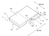
- FIG. 1A is a perspective view schematically showing an embodiment of a shunt resistance device for current detection.
- FIG. 1B is a perspective view of the shunt resistance device shown in FIG. 1A when viewed from the back side.
- FIG. 1C is a side view of the shunt resistance device shown in FIG. 1A. It is an exploded perspective view of the shunt resistor shown in FIGS. 1A to 1C.
- FIG. 3A is a perspective view schematically showing another embodiment of the shunt resistance device.
- FIG. 3B is a side view of the shunt resistance device shown in FIG. 3A.
- 3 is a perspective view showing a state in which the shunt resistor is removed from the shunt resistor device shown in FIGS. 3A and 3B.
- FIG. 1A is a perspective view schematically showing an embodiment of a shunt resistance device for current detection.
- FIG. 1B is a perspective view of the shunt resistance device shown in FIG. 1A when viewed from
- FIG. 5A is a diagram showing the potential distribution of a portion located directly above the resistor of the main body portion when the jumper element does not have a protruding portion.
- FIG. 5B is a diagram for explaining the simulation conditions of FIG. 5A. It is a figure which shows the state which a plurality of wirings for voltage detection are connected to a jumper element.
- FIG. 7A is a diagram showing the potential distribution in the portion of the main body of the shunt resistor described with reference to FIGS. 1 and 2 located directly above the resistor and the protruding portion.
- FIG. 7B is a diagram for explaining the simulation conditions of FIG. 7A.
- R It is a graph showing the change depending on the measurement position of. It is a perspective view which shows the other embodiment of the shunt resistance apparatus schematically. It is a perspective view which shows typically the shunt resistor of FIG. It is a perspective view which shows the other embodiment of the shunt resistance apparatus schematically. It is an exploded perspective view of the shunt resistance apparatus shown in FIG.
- a shunt resistor is defined as a device for current detection, including at least a shunt resistor.
- a shunt resistor As an example of a shunt resistor, the shunt resistor itself, a shunt resistor equivalent to a shunt resistor by being mounted on a circuit board, etc., and a state in which various wirings are connected to the shunt resistor and mounted (shunt resistor). (Mounting structure) can be mentioned.
- FIG. 1A is a perspective view schematically showing an embodiment of a shunt resistance device for current detection
- FIG. 1B is a perspective view of the shunt resistance device shown in FIG. 1A when viewed from the back side
- FIG. 1C is a perspective view. Is a side view of the shunt resistance device shown in FIG. 1A.
- the shunt resistor device includes a shunt resistor 1.
- the shunt resistor device of the present embodiment is the shunt resistor 1 itself.
- the shunt resistor 1 is a plate-shaped (thin plate-shaped) resistor 5 having a predetermined thickness and width, a plate-shaped (thin plate-shaped) electrode 6 made of a conductive metal material, and a jumper element made of a conductive metal material. It is provided with 10 (also referred to as a terminal member).
- An example of the material of the resistor 5 is a low resistance alloy material such as a Cu—Mg—Ni based alloy.
- a low resistance alloy material such as a Cu—Mg—Ni based alloy.
- copper (Cu) which is a highly conductive metal, can be mentioned.
- the resistor 5 has a first surface 5a and a second surface 5b which is a surface opposite to the first surface 5a.
- the jumper element 10 is connected (or connected) to the first surface 5a of the resistor 5, and the electrode 6 is connected to the second surface 5b of the resistor 5. That is, the electrode 6, the resistor 5, and the jumper element 10 are laminated in this order in the thickness direction of the shunt resistor 1.
- the thickness direction of the shunt resistor 1 is a direction perpendicular to both the first direction and the second direction.
- the first direction is the length direction of the shunt resistor 1.
- the second direction is the width direction of the shunt resistor 1 and is the direction perpendicular to the first direction.
- the jumper element 10 includes a plate-shaped main body portion 11, a protruding portion 12 formed on the side portion of the main body portion 11, and a terminal portion 14 formed on the main body portion side first surface 11a of the main body portion 11. ..
- the main body portion 11, the protruding portion 12, and the terminal portion 14 are integrally formed of the same material.
- the resistor 5 is connected (or connected) to the first surface 11a on the main body side of the main body 11.
- FIG. 2 is an exploded perspective view of the shunt resistor 1 shown in FIGS. 1A to 1C.
- the first surface 5a and the second surface 5b of the resistor 5 are attached to the jumper element 10 and the electrode 6 by welding such as pressure welding, solder, and metal nanoparticles (silver paste using silver nanoparticles). Or, they are connected (bonded) by means such as bonding with copper paste using copper nanoparticles).
- the terminal portion 14 and the electrode 6 are subjected to surface treatment such as Sn plating in order to enable solder mounting.
- the terminal portion 14 and the resistor 5 are separated from each other in the first direction.
- the terminal portion 14 and the electrode 6 are separated from each other in the first direction.
- the first direction can be said to be the direction in which the resistor 5 and the terminal portion 14 are arranged.
- the protruding portion 12 is formed on the side portion of the main body portion 11. Specifically, the protruding portion 12 is formed on the side surface 11c of the main body portion 11 and protrudes from the side surface 11c in the second direction. The side surface 11c is a surface parallel to the first direction.
- the protrusion 12 is located at a position that does not overlap with the resistor 5. In other words, the protruding portion 12 is located at a position where it does not overlap with the resistor 5 in the thickness direction of the shunt resistor 1, and is not in direct contact with the resistor 5.
- the protrusion 12 is formed in a portion of the main body 11 located directly above the resistor 5 when the first surface 5a of the resistor 5 is on the top and the second surface 5b is on the bottom. There is. In one embodiment, the protrusion 12 may be formed on the side surface of the main body 11 parallel to the second direction.
- the protruding portion 12 has a protruding portion side first surface 12a on the same side as the main body side first surface 11a in the thickness direction of the jumper element 10 (that is, the thickness direction of the jumper element 10). Specifically, the main body side first surface 11a and the projecting portion side first surface 12a are on the same plane.
- the main body portion 11 has a main body portion side second surface 11b which is a surface opposite to the main body portion side first surface 11a, and the protruding portion 12 is a surface opposite to the protruding portion side first surface 12a. It has a second surface 12b on the protruding portion side. Specifically, the second surface 11b on the main body side and the second surface 12b on the protruding portion side are on the same plane.
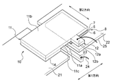
- FIG. 3A is a perspective view schematically showing another embodiment of the shunt resistance device
- FIG. 3B is a side view of the shunt resistance device shown in FIG. 3A. Since the configuration of the present embodiment, which is not particularly described, is the same as that of the above-described embodiment, the overlapping description thereof will be omitted.
- the shunt resistor device of this embodiment has a mounting structure of the shunt resistor 1. As shown in FIGS. 3A and 3B, the shunt resistor device has a wiring pattern 21 and 22 on which the shunt resistor 1 is mounted and a potential difference in the resistor 5 (between the first surface 5a and the second surface 5b). It is further provided with a pair of wires 24, 25 for detecting the generated potential difference).
- the wirings 24 and 25 function as voltage detection terminals.
- the wiring patterns 21 and 22 are mounted on a circuit board such as a printed circuit board (not shown), and the wiring patterns 21 and 22 are arranged apart from each other.
- the terminal portion 14 and the electrode 6 are connected (bonded) to the wiring pattern 21 and the wiring pattern 22 by solder or the like, respectively, and the wiring pattern 21, the shunt resistor 1, and the wiring pattern 22 form a current path.
- FIG. 4 is a perspective view showing a state in which the shunt resistor 1 is removed from the shunt resistor device shown in FIGS. 3A and 3B.
- the shunt resistor 1 is mounted in the region 28 surrounded by the dotted line in the figure.
- the leader line 23 is drawn out from the wiring pattern 22.
- the leader line 23 extends from the wiring pattern 22 toward the wiring pattern 21, and then bends and extends in the second direction.
- the wiring 24 is connected to the leader wire 23, and the wiring 25 is connected to the second surface 12b on the protruding portion side of the protruding portion 12.
- the wirings 24 and 25 are bonding wires, and the wirings 24 and 25 are connected to the leader wire 23 and the protrusion side second surface 12b by wire bonding, respectively.
- the leader line 23 and the protrusion 12 function as a bonding pad.
- the leader wire 23 and the second surface 12b on the protruding portion side are subjected to surface treatment such as Ni-P plating in order to enable wire bonding.
- the potential difference between the wiring 24 and the wiring 25 (that is, the potential difference in the resistor 5) generated by the measured current flowing through the shunt resistor 1 can be measured from the wirings 24 and 25. ..
- the potential difference in the resistor 5 is measured by a voltmeter 26 composed of a voltage measuring IC or the like.
- the leader wire 23 may be directly connected to the voltmeter 26. In that case, the leader wire 23 and the wiring 25 function as a pair of wirings for detecting the potential difference.
- FIG. 5A is a diagram showing the potential distribution of the portion located directly above the resistor 5 of the main body portion 11 when the jumper element 10 does not have the protruding portion 12.
- FIG. 5A is a contour diagram showing the simulation result of the potential distribution.
- FIG. 5B is a diagram for explaining the simulation conditions of FIG. 5A.
- the portion 16 located directly above the resistor 5 of the main body portion 11 is a portion indicated by a dot in FIG. 5B.
- the terminal portion 14 and the electrode 6 of the shunt resistor 1 are connected to the conductive lands 34 and 36, respectively, and are predetermined from the lands 34 to the lands 36 via the shunt resistor 1. Current is passed.
- a plurality of voltage detection wirings 32 may be connected to the jumper element 10. .. Even in this case, since the potential taken out differs depending on the connection position of each wiring 32, the resistance value and the temperature coefficient of resistance (TCR) detected when any one of the plurality of wirings 32 is broken. May change.
- FIG. 7A is a diagram showing the potential distribution in the portion of the main body 11 of the shunt resistor 1 directly above the resistor 5 and the protrusion 12 described with reference to FIGS. 1 and 2.
- FIG. 7A is a contour diagram showing the simulation result of the potential distribution.
- FIG. 7B is a diagram for explaining the simulation conditions of FIG. 7A.
- the object 17 of the simulation is a portion located directly above the resistor 5 of the main body portion 11 and a protruding portion 12, which is a portion indicated by a dot in FIG. 7B.
- the simulation conditions not specifically described are the same as the conditions described with reference to FIGS. 5A and 5B.
- the potential distribution of the protruding portion 12 becomes substantially uniform so that the potential of the portion of the main body portion 11 adjacent to the protruding portion 12 spreads over the protruding portion 12. That is, the potential distribution in the protrusion 12 has high uniformity. Therefore, by connecting the wiring for voltage detection to the protrusion 12 and taking out the voltage of the resistor 5, the detection voltage, the detection resistance value, and the temperature coefficient of resistance of the shunt resistance device (T. Changes in CR) can be suppressed. As a result, it is possible to suppress variations in the characteristics of the shunt resistor device depending on the connection position of the voltage detection wiring in the protrusion 12.
- the potential distribution in the main body 11 is remarkably widened in the first direction (see FIG. 1A). Therefore, by shifting the position of the protrusion 12, the detected resistance value and T.I. C. R. Can be changed.
- FIG. 8 shows the resistance value of the shunt resistor 1 and T.I. C. R. 9 is a diagram for explaining the measurement position of the shunt resistor 1
- FIG. 9 is a graph showing the change of the resistance value of the shunt resistor 1 depending on the measurement position
- FIG. 10 is a graph showing the change of the resistance value of the shunt resistor 1 depending on the measurement position.
- C. R. It is a graph which shows the change by the measurement position of.
- the terminal portion 14 and the electrode 6 are connected to the lands 34 and 36, respectively.
- 9 and 10 show an arbitrary reference point having the same potential as the land 36 and the straight lines A and B shown in FIG. 8 when a predetermined current is passed from the land 34 to the land 36 via the shunt resistor 1.
- the resistance value between one point hereinafter referred to as the measurement position
- the T.I. C. R. The simulation results of are shown.
- the set resistance value (that is, the ideal resistance value) of the shunt resistor 1 is 100 ⁇ .
- FIGS. 9 and 10 show the resistance value in the first direction and T.I. C. R.
- the vertical axis of FIG. 9 shows the resistance value at each measurement position, and the vertical axis of FIG. 10 shows the T.I. C. R. Is shown.
- the solid line represents the resistance value and T.I. C. R.
- the line represented by the broken line indicates the resistance value in the straight line B and T.I. C. R. Is shown.
- the straight line A and the straight line B are virtual straight lines extending in the first direction on the second surface 11b on the main body side and on the second surface 12b on the protruding portion side, respectively.
- the straight lines L1, L2, L3, and L4 shown in FIG. 8 indicate the positions of 0 mm, 1.5 mm, 3.0 mm, and 5.0 mm in the first direction.
- the size of the main body portion 11 and the protruding portion 12 shown in FIG. 8 is an example, and the size of each component of the shunt resistor 1 and the shunt resistor 1 is not limited to this embodiment.
- the resistance value and T.I. C. R Changes in the resistance value in the straight line A and T.I. C. R. Significantly less than the change in. That is, on the straight line B, the resistance value and T.I. C. R.
- the simulation results show that As a result, it is possible to suppress variations in the characteristics of the shunt resistor 1 (that is, variations in the characteristics of the shunt resistor device) depending on the connection position of the voltage detection wiring in the protrusion 12.
- FIG. 11 is a perspective view schematically showing another embodiment of the shunt resistor 1. Since the configuration of the present embodiment, which is not particularly described, is the same as that of the above-described embodiment, the duplicated description thereof will be omitted. In the present embodiment, the length of the protrusion 12 in the first direction is the same as the length of the resistor 5 in the first direction.
- FIG. 12 is a perspective view schematically showing still another embodiment of the shunt resistor 1. Since the configuration of the present embodiment, which is not particularly described, is the same as that of the above-described embodiment, the overlapping description thereof will be omitted.
- the jumper element 10 of the present embodiment has a slit 13 formed in the protruding portion 12.
- the slit 13 is an elongated notch. Specifically, the slit 13 extends from the side surface 12c connected to the main body portion 11 of the protrusion 12 toward the side surface 12d which is the opposite surface of the side surface 12c.
- the side surface 12c is a side surface facing the outside of the shunt resistor 1
- the side surface 12d is a side surface facing the inside of the shunt resistor 1 (the direction in which the terminal portion 14 is arranged in the first direction).
- the slit 13 is formed at the base of the protruding portion 12. In other words, the slit 13 is formed between the main body portion 11 and the protruding portion 12.
- the position of the slit 13 is not limited to the present embodiment as long as the slit 13 extends from the side surface 12c connected to the main body portion 11 of the protruding portion 12.
- FIG. 13 is a perspective view schematically showing still another embodiment of the shunt resistor 1. Since the details of the present embodiment not particularly described are the same as those of the embodiment described with reference to FIG. 12, the duplicated description will be omitted.
- the present embodiment is different from the embodiment shown in FIG. 12 in that the slit 13 extends from the side surface 12d connected to the main body portion 11 of the protruding portion 12 toward the side surface 12c.
- the position of the slit 13 is not limited to the present embodiment as long as the slit 13 extends from the side surface 12d connected to the main body portion 11 of the protruding portion 12.
- FIG. 14 is a perspective view schematically showing still another embodiment of the shunt resistor 1. Since the details of the present embodiment not particularly described are the same as those of the embodiments described with reference to FIGS. 12 and 13, the duplicated description thereof will be omitted.
- This embodiment is the same as the embodiment shown in FIGS. 12 and 13 in that a slit 13a extending from the side surface 12c toward the side surface 12d and a slit 13b extending from the side surface 12d toward the side surface 12c are formed in the protrusion 12. It's different.
- the configurations of the slits 13a and 13b, which are not particularly described, are the same as those of the slits 13 described with reference to FIGS. 12 and 13.
- the embodiments described with reference to FIGS. 11 to 14 can also be applied to the embodiments described with reference to FIGS. 3A, 3B and 4.
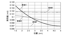
- FIG. 15 is a graph showing changes in the resistance value of the shunt resistor 1 shown in FIGS. 11 to 13 depending on the measurement position
- FIG. 16 is a graph showing the T.T. of the shunt resistor 1 shown in FIGS. 11 to 13.
- C. R. It is a graph which shows the change by the measurement position of. 15 and 16 show the resistance value between an arbitrary reference point and one point (hereinafter referred to as a measurement position) on the straight lines C, D, E, and F shown in FIGS. 11 to 13, and the shunt resistance at the measurement position.
- the simulation results of are shown.
- the simulation conditions are the same as the conditions described with reference to FIGS. 8 to 10.
- the straight lines C and D are virtual straight lines extending in the first direction on the second surface 11b on the main body side and the second surface 12b on the protruding portion side of the shunt resistor 1 shown in FIG. 11, respectively, and the straight lines E and F are , Is a virtual straight line extending in the first direction on the second surface 12b on the protruding portion side of the shunt resistor 1 shown in FIGS. 12 and 13.
- the depth (length in the first direction) of the slit 13 shown in FIGS. 12 and 13 is 2.5 mm.
- the straight lines L1, L2, and L4 indicate the positions of 0 mm, 1.5 mm, and 5.0 mm in the first direction, respectively.
- the sizes of the main body portion 11 and the protruding portion 12 shown in FIGS. 11 to 13 are examples, and the sizes of the shunt resistors 1 and the components of the shunt resistors 1 are not limited to the present embodiment.
- the horizontal axis of FIGS. 15 and 16 is the resistance value in the first direction and T.I. C. R.
- the vertical axis of FIG. 15 shows the resistance value at each measurement position, and the vertical axis of FIG. 16 shows the T.I. C. R. Is shown.
- the solid line represents the resistance value and T.I. C. R.
- the line represented by the thick broken line indicates the resistance value in the straight line D and T.I. C. R.
- the line represented by the alternate long and short dash line is the resistance value in the straight line E and T.I. C. R.
- the line represented by the thin broken line indicates the resistance value in the straight line F and T.I. C. R. Is shown.
- the resistance value and the T.I. C. R As shown in FIGS. 15 and 16, in the straight lines E and F, the resistance value and the T.I. C. R. The value of is almost unchanged. Further, when the slit 13 is inserted from the side surface 12c side, the resistance value and T.I. C. R. When the value of is increased and the slit 13 is inserted from the side surface 12d side, the resistance value and T.I. C. R. The value of is reduced. This is because, as shown in FIG. 7A, the potential on the side surface 12d side is higher than the potential on the side surface 12c side, and the potential of the portion of the main body 11 adjacent to the protrusion 12 spreads to the protrusion 12. ..
- Resistance value and T.I. C. R. Can be made smaller than the value shown in FIG. 15 (closer to the resistance value and TCR when the measurement position is on the straight line D), and the depth of the slit 13 in FIG. 13 is changed in the shallow direction. Then, the resistance value and T.I. C. R. Can be made larger than the value shown in FIG. 15 (closer to the resistance value and TCR when the measurement position is on the straight line D).
- the slit 13 described above in the protruding portion 12 the potential distribution of the protruding portion 12 becomes more uniform. Therefore, by forming the slit 13, the characteristics of the shunt resistor, that is, the resistance value of the shunt resistor and / or T.I. C. R. Can be adjusted. Specifically, by adjusting the direction in which the slit 13 is inserted and the depth, the characteristics of the shunt resistance device when the measurement position is on the second surface 12b on the protruding portion side, that is, the resistance value of the shunt resistance device and / Or T. C. R. Can be adjusted.
- the jumper element 10 and the shunt resistor may be formed separately in advance and fixed as one at the time of mounting.
- FIG. 17 is a perspective view schematically showing still another embodiment of the shunt resistance device. Since the configuration of the present embodiment, which is not particularly described, is the same as that of the above-described embodiment, the overlapping description thereof will be omitted.
- the shunt resistor device of the present embodiment includes a shunt resistor 8 and a jumper element 10 connected to the shunt resistor 8. In the present embodiment, the shunt resistor 8 and the jumper element 10 are formed separately in advance. The details of the jumper element 10 not particularly described are the same as those in the above-described embodiment.
- the first surface 11a on the main body side of the main body 11 of the present embodiment can be connected to the resistor 5 that constitutes a part of the shunt resistor 8. Specifically, the main body 11 can be connected (or connected) to the resistor 5 via the electrode 7 described later.
- FIG. 18 is a perspective view schematically showing the shunt resistor 8 of FIG. Since the configuration of the shunt resistor 8 which is not particularly described is the same as that of the shunt resistor 1, the overlapping description thereof will be omitted.
- the shunt resistor 8 is different from the shunt resistor 1 in that it includes a plate-shaped (thin plate-shaped) electrode 7 made of a conductive metal material instead of the jumper element 10.
- the material of the electrode 7 is copper (Cu), which is a highly conductive metal.
- the electrode 7 is connected to the first surface 5a of the resistor 5, and the electrode 6, the resistor 5, and the electrode 7 are laminated in this order in the thickness direction of the shunt resistor 8.
- the jumper element 10 is connected to the electrode 7.
- the main body 11 of the jumper element 10 is connected to the first surface 5a of the resistor 5. More specifically, the main body side first surface 11a of the main body 11 of the jumper element 10 is connected (or connected) to the first surface 5a of the resistor 5 via the electrode 7.
- the terminal portion 14 and the shunt resistor 8 are separated from each other in the first direction.
- the protrusion 12 is located at a position that does not overlap with the resistor 5.
- the protrusion 12 is located at a position that does not overlap with the resistor 5 in the thickness direction of the shunt resistor device, and does not come into direct contact with the shunt resistor 8.
- the first surface 11a on the main body side of the jumper element 10 is provided with welding such as pressure welding, solder, or metal nanoparticles (silver paste using silver nanoparticles or copper nanoparticles) on the electrode 7. It is connected (bonded) to the electrode 7 by means such as bonding with the copper paste used).
- FIG. 19 is a perspective view schematically showing still another embodiment of the shunt resistance device
- FIG. 20 is an exploded perspective view of the shunt resistance device shown in FIG. Since the details of the present embodiment not particularly described are the same as those of the embodiments described with reference to FIGS. 3A, 3B and 4, the duplicate description thereof will be omitted.
- This embodiment is different from the embodiment shown in FIGS. 3A, 3B and 4 in which the shunt resistance device described with reference to FIGS. 17 and 18 is mounted on the wiring patterns 21 and 22.
- the shunt resistor 8 is mounted on the wiring pattern 22
- the jumper element 10 is mounted on the shunt resistor 8
- the terminal portion 14 is connected to the wiring pattern 21.
- the wiring pattern 21, the jumper element 10, the shunt resistor 8, and the wiring pattern 22 form a current path.
- the embodiments described with reference to FIGS. 17 to 20 can be applied. Also in the embodiment described with reference to FIGS. 17 to 20, the same effect as the effect described with reference to FIGS. 7A to 16 can be obtained. Also in the embodiment described with reference to FIGS. 17 to 20, the shunt resistance device when the measurement position is on the second surface 12b on the protruding portion side by adjusting the direction in which the slit 13 is inserted and the depth. Characteristics, ie the resistance value of the shunt resistance device and / or T.I. C. R. Can be adjusted.
- the present invention is applicable to a method for adjusting the characteristics of a jumper element, a shunt resistance device, and a shunt resistance device for current detection.
Abstract
La présente invention concerne : un élément cavalier ; un dispositif de résistance de dérivation ; et un procédé d'ajustement des caractéristiques d'un dispositif de résistance de dérivation en vue d'une détection de courant. Selon la présente invention, un élément cavalier (10) permettant de constituer un dispositif de résistance de dérivation en vue d'une détection de courant est composé d'un matériau métallique conducteur. Cet élément cavalier (10) est pourvu : d'une partie de corps principal (11) qui peut être reliée à une résistance (5) qui constitue une partie d'un dispositif de résistance de dérivation ; et d'une partie saillante (12) qui est formée sur une partie latérale de la partie de corps principal (11). La partie saillante (12) est positionnée de façon à ne pas chevaucher la résistance (5).
Priority Applications (3)
| Application Number | Priority Date | Filing Date | Title |
|---|---|---|---|
| CN202180066209.6A CN116250047A (zh) | 2020-09-30 | 2021-08-11 | 跨接元件、分流电阻装置和电流检测用分流电阻装置的特性调整方法 |
| US18/028,610 US20230333143A1 (en) | 2020-09-30 | 2021-08-11 | Jumper element, shunt resistor apparatus, and method of adjusting characteristic of shunt resistor apparatus for current detection |
| DE112021005166.0T DE112021005166T5 (de) | 2020-09-30 | 2021-08-11 | Brückenelement, shunt-widerstandsvorrichtung und verfahren zur einstellung der charakteristik einer shunt-widerstandsvorrichtung zur stromerkennung |
Applications Claiming Priority (2)
| Application Number | Priority Date | Filing Date | Title |
|---|---|---|---|
| JP2020164803A JP2022056841A (ja) | 2020-09-30 | 2020-09-30 | ジャンパー素子、シャント抵抗装置、および電流検出用シャント抵抗装置の特性調整方法 |
| JP2020-164803 | 2020-09-30 |
Publications (1)
| Publication Number | Publication Date |
|---|---|
| WO2022070623A1 true WO2022070623A1 (fr) | 2022-04-07 |
Family
ID=80949918
Family Applications (1)
| Application Number | Title | Priority Date | Filing Date |
|---|---|---|---|
| PCT/JP2021/029608 WO2022070623A1 (fr) | 2020-09-30 | 2021-08-11 | Élément cavalier, dispositif de résistance de dérivation et procédé d'ajustement des caractéristiques d'un dispositif de résistance de dérivation en vue d'une détection de courant |
Country Status (5)
| Country | Link |
|---|---|
| US (1) | US20230333143A1 (fr) |
| JP (1) | JP2022056841A (fr) |
| CN (1) | CN116250047A (fr) |
| DE (1) | DE112021005166T5 (fr) |
| WO (1) | WO2022070623A1 (fr) |
Citations (5)
| Publication number | Priority date | Publication date | Assignee | Title |
|---|---|---|---|---|
| JP2012227360A (ja) * | 2011-04-20 | 2012-11-15 | Panasonic Corp | チップ型抵抗器およびその製造方法 |
| JP2013536424A (ja) * | 2010-08-26 | 2013-09-19 | イザベレンヒュッテ ホイスラー ゲー・エム・ベー・ハー ウント コンパニー コマンデイトゲゼルシャフト | 電流検出抵抗器 |
| JP2016004886A (ja) * | 2014-06-17 | 2016-01-12 | Koa株式会社 | 電流検出用抵抗器 |
| JP2016503176A (ja) * | 2013-01-16 | 2016-02-01 | ロベルト・ボッシュ・ゲゼルシャフト・ミト・ベシュレンクテル・ハフツングRobert Bosch Gmbh | 被測定抵抗器付きの測定装置 |
| JP2018132386A (ja) * | 2017-02-14 | 2018-08-23 | Koa株式会社 | 電流測定装置および電流検出用抵抗器 |
-
2020
- 2020-09-30 JP JP2020164803A patent/JP2022056841A/ja active Pending
-
2021
- 2021-08-11 DE DE112021005166.0T patent/DE112021005166T5/de active Pending
- 2021-08-11 US US18/028,610 patent/US20230333143A1/en active Pending
- 2021-08-11 CN CN202180066209.6A patent/CN116250047A/zh active Pending
- 2021-08-11 WO PCT/JP2021/029608 patent/WO2022070623A1/fr active Application Filing
Patent Citations (5)
| Publication number | Priority date | Publication date | Assignee | Title |
|---|---|---|---|---|
| JP2013536424A (ja) * | 2010-08-26 | 2013-09-19 | イザベレンヒュッテ ホイスラー ゲー・エム・ベー・ハー ウント コンパニー コマンデイトゲゼルシャフト | 電流検出抵抗器 |
| JP2012227360A (ja) * | 2011-04-20 | 2012-11-15 | Panasonic Corp | チップ型抵抗器およびその製造方法 |
| JP2016503176A (ja) * | 2013-01-16 | 2016-02-01 | ロベルト・ボッシュ・ゲゼルシャフト・ミト・ベシュレンクテル・ハフツングRobert Bosch Gmbh | 被測定抵抗器付きの測定装置 |
| JP2016004886A (ja) * | 2014-06-17 | 2016-01-12 | Koa株式会社 | 電流検出用抵抗器 |
| JP2018132386A (ja) * | 2017-02-14 | 2018-08-23 | Koa株式会社 | 電流測定装置および電流検出用抵抗器 |
Also Published As
| Publication number | Publication date |
|---|---|
| US20230333143A1 (en) | 2023-10-19 |
| JP2022056841A (ja) | 2022-04-11 |
| CN116250047A (zh) | 2023-06-09 |
| DE112021005166T5 (de) | 2023-12-21 |
Similar Documents
| Publication | Publication Date | Title |
|---|---|---|
| US10026529B2 (en) | Shunt resistor | |
| JP4138215B2 (ja) | チップ抵抗器の製造方法 | |
| US8183976B2 (en) | Resistor device and method for manufacturing same | |
| US9305687B2 (en) | Current sensing resistor | |
| CN109313218B (zh) | 分流电阻器的安装结构以及安装基板 | |
| JP2020102626A (ja) | 抵抗の温度係数が低い抵抗器 | |
| US8779887B2 (en) | Current sensing resistor | |
| WO2021220895A1 (fr) | Dispositif de détection de courant | |
| JP2013201339A (ja) | 抵抗器およびその実装構造 | |
| JP6408758B2 (ja) | ジャンパー素子 | |
| WO2022070623A1 (fr) | Élément cavalier, dispositif de résistance de dérivation et procédé d'ajustement des caractéristiques d'un dispositif de résistance de dérivation en vue d'une détection de courant | |
| WO2022244595A1 (fr) | Dispositif de détection de courant | |
| JP6652393B2 (ja) | シャント抵抗器およびシャント抵抗器を用いた電流検出装置 | |
| WO2022085255A1 (fr) | Résistance shunt et dispositif de résistance shunt | |
| JP4712943B2 (ja) | 抵抗器の製造方法および抵抗器 | |
| WO2023199611A1 (fr) | Résistance shunt et dispositif à résistance de shuntage | |
| WO2022124255A1 (fr) | Résistance shunt et sa structure de montage | |
| JP6364169B2 (ja) | シャント抵抗器及びその抵抗値測定方法 | |
| JP2002208501A (ja) | 抵抗器、その抵抗器を用いる電子部品及びそれらの使用方法 | |
| CN117355910A (zh) | 跳线芯片部件 | |
| JP2021005606A (ja) | チップ抵抗器 | |
| JP2022030815A (ja) | 電流検出装置 | |
| JPS62276801A (ja) | 混成集積回路装置 | |
| JPH08186365A (ja) | 混成集積回路装置 |
Legal Events
| Date | Code | Title | Description |
|---|---|---|---|
| 121 | Ep: the epo has been informed by wipo that ep was designated in this application |
Ref document number: 21874926 Country of ref document: EP Kind code of ref document: A1 |
|
| WWE | Wipo information: entry into national phase |
Ref document number: 112021005166 Country of ref document: DE |
|
| 122 | Ep: pct application non-entry in european phase |
Ref document number: 21874926 Country of ref document: EP Kind code of ref document: A1 |