WO2022065197A1 - D級増幅器 - Google Patents
D級増幅器 Download PDFInfo
- Publication number
- WO2022065197A1 WO2022065197A1 PCT/JP2021/034128 JP2021034128W WO2022065197A1 WO 2022065197 A1 WO2022065197 A1 WO 2022065197A1 JP 2021034128 W JP2021034128 W JP 2021034128W WO 2022065197 A1 WO2022065197 A1 WO 2022065197A1
- Authority
- WO
- WIPO (PCT)
- Prior art keywords
- signal
- pulse
- class
- input signal
- vofs
- Prior art date
- Legal status (The legal status is an assumption and is not a legal conclusion. Google has not performed a legal analysis and makes no representation as to the accuracy of the status listed.)
- Ceased
Links
Images




Classifications
-
- H—ELECTRICITY
- H03—ELECTRONIC CIRCUITRY
- H03F—AMPLIFIERS
- H03F3/00—Amplifiers with only discharge tubes or only semiconductor devices as amplifying elements
- H03F3/20—Power amplifiers, e.g. Class B amplifiers, Class C amplifiers
- H03F3/21—Power amplifiers, e.g. Class B amplifiers, Class C amplifiers with semiconductor devices only
- H03F3/217—Class D power amplifiers; Switching amplifiers
- H03F3/2173—Class D power amplifiers; Switching amplifiers of the bridge type
-
- H—ELECTRICITY
- H03—ELECTRONIC CIRCUITRY
- H03F—AMPLIFIERS
- H03F3/00—Amplifiers with only discharge tubes or only semiconductor devices as amplifying elements
- H03F3/20—Power amplifiers, e.g. Class B amplifiers, Class C amplifiers
- H03F3/21—Power amplifiers, e.g. Class B amplifiers, Class C amplifiers with semiconductor devices only
- H03F3/217—Class D power amplifiers; Switching amplifiers
-
- H—ELECTRICITY
- H03—ELECTRONIC CIRCUITRY
- H03F—AMPLIFIERS
- H03F1/00—Details of amplifiers with only discharge tubes, only semiconductor devices or only unspecified devices as amplifying elements
- H03F1/02—Modifications of amplifiers to raise the efficiency, e.g. gliding Class A stages, use of an auxiliary oscillation
- H03F1/0205—Modifications of amplifiers to raise the efficiency, e.g. gliding Class A stages, use of an auxiliary oscillation in transistor amplifiers
-
- H—ELECTRICITY
- H03—ELECTRONIC CIRCUITRY
- H03F—AMPLIFIERS
- H03F3/00—Amplifiers with only discharge tubes or only semiconductor devices as amplifying elements
- H03F3/181—Low-frequency amplifiers, e.g. audio preamplifiers
- H03F3/183—Low-frequency amplifiers, e.g. audio preamplifiers with semiconductor devices only
-
- H—ELECTRICITY
- H03—ELECTRONIC CIRCUITRY
- H03F—AMPLIFIERS
- H03F2200/00—Indexing scheme relating to amplifiers
- H03F2200/03—Indexing scheme relating to amplifiers the amplifier being designed for audio applications
-
- H—ELECTRICITY
- H03—ELECTRONIC CIRCUITRY
- H03F—AMPLIFIERS
- H03F2200/00—Indexing scheme relating to amplifiers
- H03F2200/351—Pulse width modulation being used in an amplifying circuit
Definitions
- This disclosure relates to a class D amplifier that drives a load with a pulse width modulated pulse based on an input signal.
- a first pulse whose pulse width widens according to a positive change of the input signal and a second pulse whose pulse width widens according to a negative change of the input signal are generated, and the first and second pulses are generated.
- a class D amplifier that drives a load such as a speaker by a pulse is known.
- the "signal" in the present disclosure indicates the signal itself or the voltage of the signal.
- the signal current is specified as "signal current”.
- the input signal is sandwiched between the lower limit of the input signal that generates the first pulse and the upper eye of the input signal that generates the second pulse.
- both the pulse width of the first pulse and the pulse width of the second pulse are shortened, and power consumption can be reduced.
- the small signal region in the small signal region, a first pulse having a wide pulse width and a second pulse having a narrow pulse width are output in response to a positive change in the instantaneous value of the input signal.
- the large signal area other than the small signal area only one of the pulses is output. Therefore, the small signal region is a high gain region where the open loop gain of the class D amplifier is high, and the large signal region where the absolute value of the input signal is large is a low gain region where the open loop gain is lower than the high gain region.
- the input / output characteristics of the class amplifier are non-linear and there is a lot of total harmonic distortion.
- Patent Document 1 discloses a technique for suppressing distortion of the output signal of a class D amplifier.
- an offset voltage corresponding to the distortion generated in the output stage of the class D amplifier is applied to the input signal of the pulse width modulation section of the class D amplifier.
- This disclosure has been made in view of the circumstances described above, and an object thereof is to provide a technical means for reducing power consumption in a small signal region while suppressing deterioration of total harmonic distortion in a class D amplifier. And.
- This disclosure is a class D amplifier that amplifies an input signal, and is a control circuit that generates a control signal that changes according to the signal level of the input signal, and the pulse width thereof is the signal level according to the control signal.
- a class D amplifier including a second generation circuit that generates a second pulse, which becomes wider as the instantaneous value of the input signal becomes lower.
- FIG. 1 is a block diagram showing a configuration of a class D amplifier 1 according to an embodiment of the present disclosure.
- the positive input of the speaker SP is connected to the first output terminal 151 of the class D amplifier 1 via the LC filter 161 and the negative input of the speaker SP is connected to the second output terminal 152 via the LC filter 162.
- the LC filters 161 and 162 serve to remove high frequency components of the pulse output from the first output terminal 151 and the second output terminal 152.
- the speaker SP is an example of a load, and may be another load such as a motor or a light emitting element.
- the first-stage amplifier includes a subtraction unit 111 and an integration unit 112.
- the subtraction unit 111 subtracts the feedback signal Vf output by the feedback unit 170 from the input signal Ain given via the input terminal 101, and outputs a signal indicating the subtraction result.
- the integrating unit 112 integrates and outputs the output signal of the subtracting unit 111.
- the first-stage amplifier has a larger gain in the lower frequency range, and the output of the class D amplifier 1 is negatively fed back to its input.
- the output signal of this first stage amplifier is given to the addition units 121P and 121N as an input signal Vin.
- This input signal Vin is a signal obtained by correcting the input signal Ain based on the feedback signal Vf, and changes following the input signal Ain.
- the control circuit 120 generates negative offset voltage ⁇ Vofs and positive offset voltage + Voffs whose absolute value becomes smaller as the signal level increases according to the signal level of the input signal Ain as control signals.
- the signal level is a level indicating the strength of the signal, and is extracted as, for example, an envelope of the amplitude of the signal, a peak level of the signal, or the like. More specifically, in the present embodiment, the negative offset voltage-Vofs and the positive offset voltage + Voffs, which are control signals, follow the rising edge of the signal level of the input signal Ain without delay, and their absolute values become smaller. It follows the falling edge of the signal level with a predetermined time constant, and its absolute value gradually increases.
- the addition unit 121P outputs a signal Vin-Vofs obtained by adding a negative offset voltage-Vofs to the input signal Vin to the first pulse generation unit 131P.
- the addition unit 121N outputs a signal Vin + Vofs obtained by adding a positive offset voltage + Vofs to the input signal Vin to the second pulse generation unit 131N.
- This addition corresponds to a voltage shift. That is, Vin-Vofs is a signal obtained by shifting the input signal Vin downward by the control signal Vofs, and Vin + Vofs is a signal obtained by shifting the input signal Vin upward by the control signal Vofs.
- the carrier wave generation unit 132 is a circuit that generates a periodic carrier wave C.
- the carrier wave C has a section in which the value rises from the negative peak value ⁇ Vm to the positive peak value + Vm in each period, and a section in which the value falls from the positive peak value + Vm to the negative peak value ⁇ Vm. It is a triangular wave.
- the first pulse generation unit 131P and the second pulse generation unit 131N are each configured by a comparator.
- the carrier wave C generated by the carrier wave generation unit 132 is output to the first pulse generation unit 131P and the second pulse generation unit 131N.
- the first pulse generation unit 131P is in the ON state (high level) during the period when the Vin-Vofs is higher than C, and is in the OFF state (OFF state) in the other period, as compared with the signal Vin-Vofs output by the addition unit 121P and the carrier wave C.
- the first pulse Vp which becomes low level) is output.
- the signal Vin is a signal obtained by amplifying the input signal Ain by the first-stage amplifier.
- the first pulse generation unit 131P outputs the first pulse Vp based on the carrier wave C, the control signal-Vofs, and the signal Vin.
- the first pulse generation unit 131P is a first generation circuit that generates the first pulse Vp, and the pulse width in each cycle of the first pulse Vp becomes narrower as the control signal ⁇ Vofs becomes lower ( The duty ratio decreases (decreases), and increases as the instantaneous value of the input signal Vin increases (duty ratio increases).
- the second pulse generation unit 131N is in the ON state (high level) during the period when Vin + Vofs is lower than C, and is in the OFF state (low level) in the other period, as compared with the signal Vin + Vofs output by the addition unit 121N and the carrier wave C. ),
- the second pulse Vn is output. Therefore, it can be said that the second pulse generation unit 131N outputs the second pulse Vn based on the carrier wave C, the control signal + Vofs, and the signal Vin.
- the second pulse generation unit 131N is a second generation circuit that generates the second pulse Vn, and the pulse width in each cycle of the second pulse Vn becomes narrower as the control signal + Vofs becomes higher (duty).
- the ratio decreases) and increases as the instantaneous value of the input signal Vin decreases (duty ratio increases).
- “high signal” indicates that the voltage of the signal is high
- “low signal” indicates that the voltage of the signal is low.
- the output stage 140 is a circuit that amplifies the first pulse Vp and the second pulse Vn and outputs them as the first pulse P and the second pulse N to the first output terminal 151 and the second output terminal 152.
- the speaker SP which is a load, is connected between the first output terminal 151 and the second output terminal 152 of the output stage 140 by a BTL (Bridge Tied Load).
- BTL Bridge Tied Load
- the first pulse P and the second pulse N have opposite polarities. That is, the combined pulse PN of the first pulse P and the pulse obtained by reversing the second pulse N is given to the load.
- the feedback unit 170 generates the above-mentioned feedback signal Vf by removing the high frequency components of the first pulse P and the second pulse N, and supplies the feedback signal Vf to the subtraction unit 111. By performing the negative feedback of the feedback signal Vf, the waveform Vsp given to the speaker SP has the same shape as the input signal Ain.
- FIG. 2 is a block diagram showing the configuration of the control circuit 120.
- the full-wave rectifier unit 122 full-wave rectifies the input signal Ain and outputs it.
- the envelope follower 123 outputs a level signal Venv that rises following the peak value without delay during the period when the peak value of the output signal of the full-wave rectifier unit 122 rises, and a predetermined time constant during the period when the peak value falls. Outputs the level signal Env that follows and falls.
- the level signal Venv indicates the signal level of the input signal Ain.
- the level adjustment unit 124 is a circuit that generates a negative offset voltage ⁇ Vofs and a positive offset voltage + Voffs, which are control signals whose absolute value decreases as the signal Venv increases, respectively, based on the level signal Venv from the envelope follower 123.
- the control circuit 120 is a circuit that generates a negative offset voltage ⁇ Vofs and a positive offset voltage + Voffs, which are control signals whose absolute value becomes smaller as the signal level of the input signal Ain increases.
- the level adjusting unit 124 has a positive offset voltage + Vofs obtained by subtracting a value corresponding to the level signal Venv from the value corresponding to the positive peak value of the carrier wave C + Vm and further subtracting a predetermined margin, and this voltage.
- a negative offset voltage with the polarity of + Vofs reversed-Vofs is output.
- the positive offset voltage + Vofs becomes zero when the subtraction result is negative, and does not take a negative value.
- how to determine the voltage of the margin is arbitrary.
- the margin may be a constant value or may be changed according to the level signal Venv. That is, the positive offset voltage + Voffs and the negative offset voltage-Vofs may change curvilinearly with respect to the change in the level signal Venv.
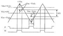
- FIG. 3 is a waveform diagram showing the operation of the first pulse generation unit 131P and the second pulse generation unit 131N.
- the first pulse generation unit 131P outputs the first pulse Vp which is turned ON (high level) during the period when Vin-Vofs is higher than C as compared with the signal Vin-Vofs and the carrier wave C.
- the second pulse generation unit 131N outputs a second pulse Vn that is ON (high level) during a period when Vin + Vofs is lower than C, as compared with the signal Vin + Vofs and the carrier wave C.
- the pulse width of the first pulse Vp becomes wider according to the change of the input signal Vin in the positive direction, and the pulse width becomes narrower according to the change of the control signal Vofs in the positive direction.
- the pulse width becomes wider according to the change of the input signal Vin in the negative direction, and the pulse width becomes narrower according to the change of the control signal Vofs in the positive direction.
- control circuit 120 controls the high gain region HG by changing the offset voltages ⁇ Vofs and +Vofs, which are control signals, according to the input signal Ain, and the class D amplifier 1 is always in the high gain region HG. To operate in.
- FIG. 4 is a diagram showing an example of input / output characteristics of the level adjusting unit 124 in the control circuit 120.
- the horizontal axis is the output voltage Venv of the envelope follower 123
- the vertical axis is the offset voltage ⁇ Vofs or + Voffs.
- the class D amplifier 1 operates in the high gain region HG. Therefore, in order to operate the class D amplifier 1 in the high gain region HG, it is necessary to make the offset voltage Vofs (absolute value) smaller than the value obtained by subtracting the signal level of the input signal Vin from the peak value + Vm of the carrier wave C. ..
- the level adjusting unit 124 subtracts the voltage corresponding to the level signal Venv from the positive peak value + Vm of the carrier wave C, and further subtracts a predetermined margin, and based on the value, the positive offset voltage + Vofs (and). Negative offset voltage-Vofs) is generated.
- the absolute value (offset voltage Vofs) of the positive offset voltage + Vofs and the negative offset voltage-Vofs is a predetermined maximum value. It becomes Vofs_max.
- This maximum value Vofs_max is a voltage obtained by subtracting a predetermined margin from the peak value + Vm (for example, 0.9V) of the carrier wave C, and is, for example, about 0.76V in FIG.
- the positive offset voltage + Vofs drops substantially linearly with respect to the rise of the voltage Venv to 0V.
- the negative offset voltage-Vofs rises substantially linearly and approaches 0V.
- the positive offset voltage + Voffs and the negative offset voltage ⁇ Vofs reach 0V.
- the input signal Ain for example, the absolute value is 9V
- the positive offset voltage + Vofs and the negative offset voltage ⁇ Vofs are 0V.
- the value of the transition voltage is calculated based on the voltage Vm (absolute value), the margin, the closed loop gain (Vsp / Ain) of the class D amplifier 1, and the gain (Vsp / Vin) after the output of the integrator. You may. Further, the input / output characteristics of FIG. 4 may be determined based on the voltage Vm (absolute value) and the calculated transition voltage.
- FIG. 5 is a diagram showing the operation of the class D amplifier 1 performed under the control of the control circuit 120 as described above.
- the upper part is a diagram showing the input / output characteristics of the class D amplifier 1 when the signal level of the input signal Ain is changed in various ways.
- the horizontal axis is the signal Vin
- the vertical axis is the pulse width of the first pulse P, the second pulse N, or their combined pulse PN.
- the operation of the class D amplifier 1 when the input signal Ain gradually rises from the signal level of no signal will be described.
- the signal level of the input signal Ain is almost zero (no signal)
- the voltage Venv applied to the level adjustment unit 124 becomes 0V
- the positive offset voltage + Vofs becomes the maximum value + Vofs_max
- the negative offset voltage- Vofs becomes a voltage-Vofs_max whose polarity is reversed.
- the lower limit of the range of the input signal Vin to which the first pulse P is output is ⁇ Vm + Vofs_max
- the upper limit of the range of the input signal Vin to which the second pulse N is output is + Vm-Vofs_max. Therefore, the input / output characteristics of the class D amplifier 1 are shown on the upper left side of FIG.
- the offset voltage Vofs which is a control signal
- the power consumption of the class D amplifier 1 when there is no signal can be reduced.
- the width of the high gain region HG gradually widens as the signal level of the input signal Ain rises. More specifically, when the signal level of the input signal Ain rises and the voltage Venv applied to the level adjustment unit 124 rises, the lower limit value of the high gain region HG so that the signal Vin falls within the high gain region HG- The offset voltage Vofs that determines Vm + Vofs and the upper limit + Vm-Vofs is reduced. Therefore, in the process of increasing the signal level of the input signal Ain, the signal Vin is always contained in the high gain region HG, and the class D amplifier 1 always operates in the high gain region HG. Therefore, according to the present embodiment, deterioration of the total harmonic distortion can be suppressed.
- the positive offset voltage + Vofs and the negative offset voltage ⁇ Vofs are 0V. become.
- the positive offset voltage + Vofs and the negative offset voltage-Vofs maintain 0 V.
- the input / output characteristics of the class D amplifier 1 are shown on the upper right side of FIG. 5, and when the signal level exceeds the maximum value Am, the outputs of the first pulse generating section 131P and the second pulse generating section 131N are clipped. It will be in the state of. The operation at the time of this clip is the same as that of a general class D amplifier.
- the control circuit 120 in the present embodiment is provided with an envelope follower 123, and the offset voltage Vofs, which is a control signal, follows the rise of the signal level of the input signal Ain without delay and decreases, so that the signal level rises. It follows the decline with a predetermined time constant and gradually increases.
- a time constant of about 10 to 30 seconds is appropriate. That is, when the signal level of the input signal Ain drops, the input / output characteristics of the class D amplifier 1 change from those shown on the upper right side of FIG. 5 to those shown in the upper center, and further shown in the upper center of FIG. Gradually transitions from to the one shown on the left side of the upper row. Therefore, according to the present embodiment, it is possible to avoid an increase in distortion due to frequent changes in the offset voltage Vofs.
- the class D amplifier 1 in the class D amplifier 1, it is possible to reduce the power consumption in the small signal region while suppressing the deterioration of the total harmonic distortion.
- This disclosure is applicable to a wide range of class D amplifiers such as high output class D amplifiers exceeding 100 W and low output class D amplifiers mounted on mobile phones and the like.
- LC filters 161 and 162 may be omitted.
- the first pulse generation unit 131P and the second pulse generation unit 131N generate two pulses by comparing a signal obtained by adding positive and negative offset voltages to an input signal and a carrier wave.
- the first pulse generator 131P and the second pulse generator 131N may generate two pulses by comparing the input signal with the carrier with positive and negative offset voltages added. good. That is, the first pulse generation unit 131P generates the first pulse Vp by comparing the input signal Vin with the carrier wave C + Vofs shifted upward by the control signal, and the second pulse generation unit 131N generates the input signal.
- the second pulse Vn may be output by comparing Vin with the carrier wave C-Vofs shifted downward by the control signal.
- two pulses may be generated by comparing the threshold value with the two signals obtained by adding the positive and negative offset voltages and the carrier wave to the input signal.
- a triangular wave is used as the carrier wave, but a sawtooth wave may be used.
Landscapes
- Engineering & Computer Science (AREA)
- Power Engineering (AREA)
- Multimedia (AREA)
- Amplifiers (AREA)
Abstract
D級増幅器において全高調波歪率の悪化を抑制しつつ小信号領域における消費電力を低減する。 入力信号Ainを増幅するD級増幅器1であって、入力信号Ainの信号レベルに応じて小さくなる制御信号Vofsを生成する制御回路120と、第1パルスPを生成する第1生成回路131Pであって、その第1パルスPのパルス幅は、制御信号Vofsに応じて狭くなり、かつ、入力信号Ainの瞬時値が低いほど広くなる、第1生成回路131Pと、第2パルスNを生成する第2生成回路131Nであって、その第2パルスNのパルス幅が、制御信号Vofsに応じて狭くなり、かつ、入力信号Ainの瞬時値が低いほど広くなる、第2生成回路131Nと、を備える。
Description
この開示は、入力信号に基づいてパルス幅変調されたパルスにより負荷を駆動するD級増幅器に関する。
入力信号の正方向への変化に応じてパルス幅が広くなる第1パルスと、入力信号の負方向への変化に応じてパルス幅が広くなる第2パルスとを発生し、第1および第2パルスによりスピーカ等の負荷を駆動するD級増幅器が知られている。なお、本開示の「信号」は、信号自体または信号の電圧を示す。 信号の電流は「信号の電流」と明記される。
ある種のフィルタレス型D級増幅器では、入力信号の瞬時値(電圧)が0に近い小信号領域において、第1パルスが出力される入力信号の範囲と、第2パルスが出力される入力信号の範囲とを重複させている。
入力信号の絶対値が小さい小信号領域において、入力信号は、第1パルスを発生させる入力信号の下限と、第2パルスを発生させる入力信号の上眼との間に挟まれている。小信号領域では第1パルスのパルス幅および第2パルスのパルス幅の両方が短くなり、消費電力を低減できる。
ところで、上述した従来のD級増幅器において、小信号領域では、入力信号の瞬時値の正方向の変化に応じてパルス幅が広くなる第1パルスと、パルス幅が狭くなる第2パルスが出力され、小信号領域以外の大信号領域ではそのうちの一方のパルスだけが出力される。このため、小信号領域は、D級増幅器の開ループゲインが高い高ゲイン領域となり、入力信号の絶対値が大きい大信号領域は、高ゲイン領域よりも開ループゲインが低い低ゲイン領域となり、D級増幅器の入出力特性がノンリニアで全高調波歪が多い。
D級増幅器の出力信号の歪を抑制する技術に関しては、例えば特許文献1に開示がある。この特許文献1に開示の技術では、D級増幅器の出力段において発生する歪に応じたオフセット電圧をD級増幅器のパルス幅変調部の入力信号に与えている。
しかしながら、上述した従来のD級増幅器の出力段のノンリニア特性により発生する歪は、入力信号のシフト量(オフセット)を調整したとしても抑制することができない。
この開示は、以上説明した事情に鑑みてなされたものであり、D級増幅器において全高調波歪率の悪化を抑制しつつ小信号領域における消費電力を低減する技術的手段を提供することを目的とする。
この開示は、入力信号を増幅するD級増幅器であって、前記入力信号の信号レベルに応じて変化する制御信号を生成する制御回路と、そのパルス幅が、前記制御信号に応じて前記信号レベルが低いほど狭くなり、かつ、前記入力信号の瞬時値が高いほど広くなる、第1パルスを生成する第1生成回路と、そのパルス幅が、前記制御信号に応じて前記信号レベルが低いほど狭くなり、かつ、前記入力信号の瞬時値が低いほど広くなる、第2パルスを生成する第2生成回路とを備えたD級増幅器を提供する。
以下、図面を参照し、この開示の実施形態を説明する。
図1は、この開示の一実施形態によるD級増幅器1の構成を示すブロック図である。D級増幅器1の第1出力端子151にLCフィルタ161を介してスピーカSPの正側入力が、第2出力端子152にLCフィルタ162を介してスピーカSPの負側入力が接続されている。LCフィルタ161およぶ162は、第1出力端子151および第2出力端子152から出力されるパルスの高域成分を除去する役割を果たす。スピーカSPは負荷の
一例であり、モーターや発光素子など、他の負荷でもよい。
一例であり、モーターや発光素子など、他の負荷でもよい。
図1において、初段増幅器は減算部111と積分部112とを備える。減算部111は、入力端子101を介して与えられる入力信号Ainから帰還部170が出力する帰還信号Vfを減算し、減算結果を示す信号を出力する。積分部112は、減算部111の出力信号を積分して出力する。このように、初段増幅器は、低域ほど大きいゲインを有し、かつ、その入力にD級増幅器1の出力が負帰還されている。この初段増幅器の出力信号は、入力信号Vinとして加算部121Pおよび121Nに与えられる。この入力信号Vinは、帰還信号Vfに基づいて入力信号Ainを補正した信号であり、入力信号Ainに追従して変化する。制御回路120は、入力信号Ainの信号レベルに応じて、その信号レベルが大きくなるほど絶対値の小さくなる負のオフセット電圧-Vofsおよび正のオフセット電圧+Vofsを制御信号として発生する。信号レベルは、その信号の強度を示すレベルであり、例えば、信号の振幅のエンベロープや、信号のピークレベルなどとして抽出される。さらに詳述すると、本実施形態において、制御信号である負のオフセット電圧-Vofsおよび正のオフセット電圧+Vofsは、入力信号Ainの信号レベルの立ち上がりに遅滞なく追従してその絶対値が小さくなり、その信号レベルの立ち下がりに所定の時定数をもって追従してその絶対値が徐々に大きくなる。加算部121Pは、入力信号Vinに負のオフセット電圧-Vofsを加算した信号Vin-Vofsを第1パルス発生部131Pに出力する。加算部121Nは、入力信号Vinに正のオフセット電圧+Vofsを加算した信号Vin+Vofsを第2パルス発生部131Nに出力する。なお、この加算は、電圧シフトに相当する。つまり、Vin-Vofsは、入力信号Vinを制御信号Vofsだけ下にシフトして得られる信号であり、また、Vin+Vofsは、入力信号Vinを制御信号Vofsだけ上にシフトして得られる信号である。
搬送波生成部132は、周期的な搬送波Cを生成する回路である。本実施形態において、搬送波Cは、各周期に値が負のピーク値-Vmから正のピーク値+Vmに立ち上がる区間と、正のピーク値+Vmから負のピーク値-Vmに立ち下がる区間とを有する三角波である。
第1パルス生成部131Pおよび第2パルス生成部131Nは、各々コンパレータにより構成されている。第1パルス生成部131Pおよび第2パルス生成部131Nには、搬送波生成部132で生成された搬送波Cが出力される。第1パルス生成部131Pは、加算部121Pが出力する信号Vin-Vofsと搬送波Cと比較し、Vin-VofsがCより高い期間にON状態(ハイレベル)となり、それ以外の期間でOFF状態(ローレベル)となる第1パルスVpを出力する。ここで、信号Vinは、入力信号Ainを初段増幅器で増幅した信号である。従って、第1パルス生成部131Pは、搬送波C、制御信号-Vofs及び信号Vinに基づいて第1パルスVpを出力する、ということができる。この第1パルス生成部131Pは、第1パルスVpを生成する第1生成回路であって、その第1パルスVpの各周期におけるパルス幅は、制御信号-Vofsが低くなるに応じて狭くなり(デューティ比が下降)、かつ、入力信号Vinの瞬時値が高くなるにつれて広くなる(デューティ比が上昇)。また、第2パルス生成部131Nは、加算部121Nが出力する信号Vin+Vofsと搬送波Cと比較し、Vin+VofsがCより低い期間にON状態(ハイレベル)となり、それ以外の期間でOFF状態(ローレベル)となる第2パルスVnを出力する。従って、第2パルス生成部131Nは、搬送波C、制御信号+Vofs及び信号Vinに基づいて第2パルスVnを出力する、ということができる。この第2パルス生成部131Nは、第2パルスVnを生成する第2生成回路であって、その第2パルスVnの各周期におけるパルス幅が、制御信号+Vofsが高くなるに応じて狭くなり(デューティ比が下降)、かつ、入力信号Vinの瞬時値が低くなるにつれて広くなる(デューティ比が上昇)。ここで、「信号が高い」は、その信号の電圧が高いことを示し、「信号が低い」は、その信号の電圧が低いことを示す。
出力段140は、第1パルスVpおよび第2パルスVnを増幅し、第1パルスPおよび第2パルスNとして、第1出力端子151および第2出力端子152に出力する回路である。本実施形態では、この出力段140の第1出力端子151および第2出力端子152間に、負荷であるスピーカSPがBTL(Bridge Tied Load;ブリッジ接続負荷)で接続される。第1出力端子151からハイレベルの第1パルスPが出力されると、この第1パルスPにより、負荷には第1出力端子151から第2出力端子152に向かう電流が流れる。また、第2出力端子152からハイレベルの第2パルスNが出力されると、この第2パルスNにより、負荷には第2出力端子152から第1出力端子151に向かう電流が流れる。このように負荷に対する効果に着目すると、第1パルスPおよび第2パルスNは逆極性である。すなわち、負荷に対しては、第1パルスPと、第2パルスNを逆相化したパルスとの合成パルスP-Nが与えられる。帰還部170は、第1パルスPおよび第2パルスNの高域成分を除去することにより、上述した帰還信号Vfを生成し、減算部111に供給する。この帰還信号Vfの負帰還が行われることにより、スピーカSPに与えられる波形Vspは、入力信号Ainと同じ形になる。
図2は制御回路120の構成を示すブロック図である。この制御回路120において、全波整流部122は、入力信号Ainを全波整流して出力する。エンベロープフォロワ123は、全波整流部122の出力信号のピーク値が立ち上がる期間は、そのピーク値に遅滞なく追従して立ち上がるレベル信号Venvを出力し、ピーク値が立ち下がる期間は、所定の時定数をもって追従して立ち下がるレベル信号Venvを出力する。レベル信号Venvは、入力信号Ainの信号レベルを示す。レベル調整部124は、エンベロープフォロワ123からのレベル信号Venvに基づいて、各々信号Venvが大きくなるほどその絶対値が小さくなる制御信号である負のオフセット電圧-Vofsおよび正のオフセット電圧+Vofsを生成する回路である。つまり、制御回路120は、入力信号Ainの信号レベルが大きくなるほど、その絶対値が小さくなる制御信号である負のオフセット電圧-Vofsおよび正のオフセット電圧+Vofsを生成する回路である。さらに詳述すると、レベル調整部124は、搬送波Cの正のピーク値に対応する値+Vmからレベル信号Venvに対応する値を差し引き、さらに所定のマージンを差し引いた正のオフセット電圧+Vofsと、この電圧+Vofsの極性を反転した負のオフセット電圧-Vofsを出力する。ここで、正のオフセット電圧+Vofsは差し引き結果が負のときはゼロとなり、負の値はとらない。また、マージンの電圧をどのように定めるかは任意である。また、マージンは、一定値であってもよく、レベル信号Venvに応じて変化させてもよい。すなわち、正のオフセット電圧+Vofsおよび負のオフセット電圧-Vofsは、レベル信号Venvの変化に対して曲線的に変化してもよい。
次に本実施形態の動作を説明する。図3は第1パルス発生部131Pおよび第2パルス発生部131Nの動作を示す波形図である。上述したように、第1パルス生成部131Pは、信号Vin-Vofsと搬送波Cと比較し、Vin-VofsがCより高い期間にON(ハイレベル)となる第1パルスVpを出力する。また、第2パルス生成部131Nは、信号Vin+Vofsと搬送波Cと比較し、Vin+VofsがCより低い期間にON(ハイレベル)となる第2パルスVnを出力する。従って、第1パルスVpは、入力信号Vinの正方向への変化に応じてパルス幅が広くなり、制御信号Vofsの正方向への変化に応じてパルス幅が狭くなる。また、第2パルスPは、入力信号Vinの負方向への変化に応じてパルス幅が広くなり、制御信号Vofsの正方向への変化に応じてパルス幅が狭くなる。これらの第1パルスVpおよび第2パルスVnは出力段140で増幅され、第1パルスPおよび第2パルスNとして出力される。
次に第1パルスPが出力される入力信号Vinの範囲および第2パルスNが出力される入力信号Vinの範囲について説明する。仮にVin=0Vとする。この場合、搬送波Cの負のピーク-Vmと信号Vin-Vofsとの間には余裕Vm-Vofsがある。そして、入力信号Vinを0Vから余裕Vm-Vofsだけ負方向に変化させると、第1パルスPのパルス幅が0となる。すなわち、第1パルスPが出力される入力信号Vinの範囲の下限値は0V-(Vm-Vofs)となる。一方、搬送波Cの正のピーク+Vmと信号Vin+Vofsとの間には余裕Vm-Vofsがある。そして、入力信号Vinを0Vから余裕Vm-Vofsだけ正方向に変化させると、第2パルスNのパルス幅が0となる。すなわち、第2パルスNが出力される入力信号Vinの範囲の上限値は0V+(Vm-Vofs)となる。従って、入力信号Vinが変化する範囲のうち、第1パルスVpおよび第2パルスVnの両方が出力される範囲、すなわち、高ゲイン領域HGは、-Vm+Vofsから+Vm-Vofsの範囲である。
本実施形態では、制御回路120が、入力信号Ainに応じて制御信号であるオフセット電圧-Vofsおよび+Vofsを変化させることにより、高ゲイン領域HGを制御し、D級増幅器1を常に高ゲイン領域HGにおいて動作させる。
図4は制御回路120におけるレベル調整部124の入出力特性の例を示す図である。図4において、横軸はエンベロープフォロワ123の出力電圧Venv、縦軸はオフセット電圧-Vofsまたは+Vofsである。
本実施形態において、加算部121Pおよび121Nに与えられる入力信号Vinの瞬時値が下限値-Vm+Vofsから上限値+Vm-Vofsの範囲にあれば、D級増幅器1は高ゲイン領域HGにおいて動作する。従って、D級増幅器1を高ゲイン領域HGにおいて動作させるためには、オフセット電圧Vofs(絶対値)を搬送波Cのピーク値+Vmから入力信号Vinの信号レベルを差し引いた値よりも小さくする必要がある。そこで、本実施形態において、レベル調整部124は、搬送波Cの正のピーク値+Vmからレベル信号Venvに応じた電圧を差し引き、さらに所定のマージンを差し引いた値に基づき、正のオフセット電圧+Vofs(および負のオフセット電圧-Vofs)を生成する。
入力信号Ainの信号レベルが無信号であり、エンベロープフォロワ123の出力電圧Venvが0Vである場合、正のオフセット電圧+Vofsおよび負のオフセット電圧-Vofsの絶対値(オフセット電圧Vofs)は所定の最大値Vofs_maxとなる。この最大値Vofs_maxは、搬送波Cのピーク値+Vm(例えば0.9V)から所定のマージンを差し引いて得られる電圧であり、例えば、図4では約0.76Vである。
入力信号Ainの信号レベルが上昇し、エンベロープフォロワ123の出力電圧Venvが上昇すると、図4に示すように、電圧Venvの上昇に対して、正のオフセット電圧+Vofsは略直線的に低下して0Vに近づき、負のオフセット電圧-Vofsは略直線的に上昇して0Vに近づく。そして、図4に示す例では、電圧Venvが遷移電圧(例えば、9V)になると、正のオフセット電圧+Vofsおよび負のオフセット電圧-Vofsが0Vに到達する。この例の遷移電圧である9Vは、積分部112が出力する信号Vinが搬送波Cの正のピーク値+Vm=0.9Vまたは負のピーク値-Vm=-0.9Vとなるときの入力信号Ainの最大値Am(絶対値)に基いて、決められる。従って、図4に示す例では、値Amからマージンを減算した信号レベルの入力信号Ain(例えば、絶対値が9V)が与えられた場合に正のオフセット電圧+Vofsおよび負のオフセット電圧-Vofsが0Vになる。さらに、遷移電圧の値は、電圧Vm(絶対値)と、マージンと、D級増幅器1の閉ループゲイン(Vsp/Ain)と、積分器の出力以降のゲイン(Vsp/Vin)とに基いて算出してもよい。また、図4の入出力特性は、電圧Vm(絶対値)と算出された遷移電圧とに基いて決めてもよい。
図5は以上のような制御回路120の制御の下で行われるD級増幅器1の動作を示す図である。図5において上段は、入力信号Ainの信号レベルを各種変化させた場合のD級増幅器1の入出力特性を各々示す図である。これらの図において、横軸は信号Vin、縦軸は第1パルスP、第2パルスNまたはそれらの合成パルスP-Nのパルス幅である。
まず、入力信号Ainが無信号の信号レベルから徐々に立ち上がる場合のD級増幅器1の動作を説明する。入力信号Ainの信号レベルがほぼゼロ(無信号)である場合、レベル調整部124に与えられる電圧Venvは0Vとなり、上述したように正のオフセット電圧+Vofsは最大値+Vofs_maxとなり、負のオフセット電圧-Vofsはその極性を反転した電圧-Vofs_maxとなる。この結果、第1パルスPが出力される入力信号Vinの範囲の下限値は-Vm+Vofs_maxとなり、第2パルスNが出力される入力信号Vinの範囲の上限値は+Vm-Vofs_maxとなる。従って、D級増幅器1の入出力特性は、図5の上段左側に示すものとなる。
このように入力信号Ainが無信号ないしそれに近い状態である場合、制御信号であるオフセット電圧Vofsが最大値とされることにより、高ゲイン領域HGの下限値および上限値は0に最も接近した値とされ、高ゲイン領域HGの幅は最小値とされる。そして、無信号時においては、加算部121Pおよび121Nに与えられる入力信号Vinがほぼ0Vになるので、第1パルス発生部131Pに与えられる入力信号はVin-Vofs=-Vofs_max、第2パルス発生部131Nに与えられる入力信号はVin+Vofs=+Vofs_maxとなる。従って、図5の上段左側に示す例では、第1パルスPおよび第2パルスNのデューティ比は約10%になる。このように本実施形態によれば、無信号時におけるD級増幅器1の消費電力を低減できる。
入力信号Ainの信号レベルがいくらか上昇し、かつ、その信号レベルが最大値Amの半分くらいの状況では、D級増幅器1の入出力特性は、図5の上段中央に示すものとなる。
ここで、高ゲイン領域HGの幅は、入力信号Ainの信号レベルの上昇に応じて徐々に広くなる。さらに詳述すると、入力信号Ainの信号レベルが上昇して、レベル調整部124に与えられる電圧Venvが上昇すると、信号Vinが高ゲイン領域HG内に収まるように、高ゲイン領域HGの下限値-Vm+Vofsおよび上限値+Vm-Vofsを決定するオフセット電圧Vofsが減少される。従って、入力信号Ainの信号レベルが上昇する過程において、信号Vinは常に高ゲイン領域HG内に収まり、D級増幅器1は常に高ゲイン領域HGにおいて動作する。従って、本実施形態によれば、全高調波歪率の劣化を抑制できる。
入力信号Ainの信号レベルがさらに上昇し、レベル調整部124に与えられる電圧Venvが遷移電圧(図4に示す例では9V)に到達すると、正のオフセット電圧+Vofsおよび負のオフセット電圧-Vofsは0Vになる。この結果、第1パルスPが出力される入力信号Vinの範囲の下限値は-Vm+Vofs=-Vm+0V=-Vmとなり、第2パルスVnが出力される入力信号Vinの範囲の上限値は+Vm-Vofs=+Vmとなる。従って、D級増幅器1の入出力特性は、図5の上段右側に示すものとなる。この場合、入力信号Vinの瞬時値が0であるときの第1パルスPおよび第2パルスNのデューティ比は各々50%になる。
入力信号Ainの信号レベルがさらに上昇し、レベル調整部124に与えられる電圧Venvが遷移電圧を越えた場合、正のオフセット電圧+Vofsおよび負のオフセット電圧-Vofsは0Vを維持する。この場合、D級増幅器1の入出力特性は、図5の上段右側に示すものとなり、信号レベルが最大値Amを超えると、第1パルス発生部131Pおよび第2パルス発生部131Nは出力がクリップした状態となる。このクリップ時の動作は一般的なD級増幅器と同様である。
次に、入力信号Ainの信号レベルが徐々に立ち下がる場合のD級増幅器1の動作を説明する。入力信号Ainの信号レベルが立ち上がる場合は、クリップの発生を防ぐため、オフセット電圧Vofsを即時に減少する必要がある。しかし、入力信号Ainの信号レベルが立ち下がる場合は、クリップの心配はないため、オフセット電圧Vofsを即時に調整する必要はない。逆に、即時に調整することにより、オフセット電圧Vofsの変化頻度の増加によって、歪が増える虞がある。そこで、本実施形態における制御回路120は、エンベロープフォロワ123が設けられており、制御信号であるオフセット電圧Vofsは、入力信号Ainの信号レベルの立ち上がりに遅滞なく追従して減少し、信号レベルの立ち下がりに所定の時定数をもって追従して徐々に増加する。音楽信号を対象とした場合、時定数は10~30秒程度が適当である。つまり、入力信号Ainの信号レベルが立ち下がる場合に、D級増幅器1の入出力特性は、図5の上段右側に示すものから上段中央に示すものへ、さらに、図5の上段中央に示すものから上段左側に示すものへと徐々に遷移する。従って、本実施形態によれば、オフセット電圧Vofsの頻繁な変化によって歪が増えるのを回避できる。
以上説明したように、本実施形態によれば、D級増幅器1において、全高調波歪率の悪化を抑制しつつ、小信号領域における消費電力を低減できる。
<他の実施形態>
以上、この開示の実施形態について説明したが、この開示には他にも実施形態が考えられる。例えば次の通りである。
以上、この開示の実施形態について説明したが、この開示には他にも実施形態が考えられる。例えば次の通りである。
(1)この開示は、100Wを超える高出力のD級増幅器、携帯電話機等に搭載される低出力のD級増幅器等、広範囲のD級増幅器に適用可能である。低出力のD級増幅器などにおいては、LCフィルタ161および162を省略してもよい。
(2)上記実施形態において、第1パルス生成部131Pおよび第2パルス生成部131Nは、入力信号に正と負のオフセット電圧を付加した信号と搬送波を比較することにより2つのパルスを生成した。その代わりに、第1パルス生成部131Pおよび第2パルス生成部131Nは、入力信号と、搬送波に正と負のオフセット電圧を付加したものとを比較することにより、2つのパルスを生成してもよい。つまり、第1パルス生成部131Pは、入力信号Vinと、制御信号により上にシフトされた搬送波C+Vofsとを比較することにより、第1パルスVpを生成し、第2パルス生成部131Nは、入力信号Vinと、制御信号により下にシフトされた搬送波C-Vofsとを比較することにより、第2パルスVnを出力しても良い。あるいは入力信号に正と負のオフセット電圧および搬送波を加算した2つの信号と閾値とを比較することにより2つのパルスを生成してもよい。
(3)上記実施形態では、搬送波として、三角波を用いたが、鋸歯状波を用いてもよい。
1……D級増幅器、101……入力端子、111……減算部、112……積分部、120……制御回路、121P,121N……加算部、131P……第1パルス生成部、131N……第2パルス生成部、132……搬送波生成部、140……出力段、151……第1出力端子、152……第2出力端子、161,162……LCフィルタ、SP……スピーカ、170……帰還部、122……全波整流部、123……エンベロープフォロワ、124……レベル調整部。
Claims (10)
- 入力信号を増幅するD級増幅器であって、
前記入力信号の信号レベルに応じて変化する制御信号を生成する制御回路と、
そのパルス幅が、前記制御信号に応じて前記信号レベルが低いほど狭くなり、かつ、前記入力信号の瞬時値が高いほど広くなる、第1パルスを生成する第1生成回路と、
そのパルス幅が、前記制御信号に応じて前記信号レベルが低いほど狭くなり、かつ、前記入力信号の瞬時値が低いほど広くなる、第2パルスを生成する第2生成回路と、を備えたD級増幅器。 - 前記入力信号が変化する範囲における、前記第1生成回路が前記第1パルスを生成し、かつ、前記第2生成回路が第2パルスを生成する高ゲイン領域が、前記制御信号に応じて、前記信号レベルが高いほど広くなる請求項1のD級増幅器。
- 前記高ゲイン領域は、前記信号レベルに対して、所定のマージンを有している請求項2のD級増幅器。
- 前記制御信号は、前記入力信号の信号レベルの立ち上がりに遅滞なく追従して変化し、立ち下がりに所定の時定数をもって追従して変化する請求項1から請求項3の何れかのD級増幅装置。
- さらに、前記第1パルスを増幅して負荷の正側入力に供給し、前記第2パルスを増幅して前記負荷の負側入力に供給する出力段を備えた請求項1から請求項4の何れかのD級増幅装置。
- 搬送波を生成し、生成した前記搬送波を前記第1生成回路及び前記第2生成回路に出力する搬送波生成部を、さらに備え、
前記第1生成回路及び前記第2生成回路は、前記搬送波生成部によって生成された前記搬送波、前記制御回路によって生成された前記制御信号及び前記入力信号を初段増幅器で増幅した信号に基づいて、前記第1パルス及び前記第2パルスをそれぞれ生成する請求項1から請求項4の何れかのD型増幅装置。 - 前記制御回路の生成する前記制御信号は、前記入力信号の信号レベルが大きくなるほど小さくなる請求項1から請求項6の何れかのD級増幅装置。
- 前記第1生成回路は、前記制御信号だけ上にシフトされた前記信号と、前記搬送波とを比較することにより、前記第1パルスを生成し、
前記第2生成回路は、前記搬送波と、前記制御信号だけ下にシフトされた前記信号とを比較することにより、前記第2パルスを生成する請求項6または請求項7のD級増幅装置。 - 前記第1生成回路は、前記信号と、前記制御信号により上にシフトされた前記搬送波とを比較することにより、前記第1パルスを生成し、
前記第2生成回路は、前記制御信号だけ下にシフトされた前記搬送波と、前記信号とを比較することにより、前記第2パルスを生成する請求項6または請求項7のD級増幅装置。 - 前記制御回路は、前記入力信号の絶対値のピーク値が立ち上がる期間は、そのピーク値に遅滞なく追従して立ち上がり、そのピーク値が立ち下がる期間は、そのピーク値に所定の時定数をもって立ち下がるレベル信号を生成するエンベロープフォロワを備えており、
前記制御回路は、そのレベル信号に基づいて、前記制御信号を生成する請求項4のD級増幅装置。
Priority Applications (2)
| Application Number | Priority Date | Filing Date | Title |
|---|---|---|---|
| CN202180063231.5A CN116325492A (zh) | 2020-09-28 | 2021-09-16 | D类放大器 |
| US18/126,751 US12603620B2 (en) | 2020-09-28 | 2023-03-27 | Class-D amplifier |
Applications Claiming Priority (2)
| Application Number | Priority Date | Filing Date | Title |
|---|---|---|---|
| JP2020-161667 | 2020-09-28 | ||
| JP2020161667A JP7615586B2 (ja) | 2020-09-28 | 2020-09-28 | D級増幅器 |
Related Child Applications (1)
| Application Number | Title | Priority Date | Filing Date |
|---|---|---|---|
| US18/126,751 Continuation US12603620B2 (en) | 2020-09-28 | 2023-03-27 | Class-D amplifier |
Publications (1)
| Publication Number | Publication Date |
|---|---|
| WO2022065197A1 true WO2022065197A1 (ja) | 2022-03-31 |
Family
ID=80846481
Family Applications (1)
| Application Number | Title | Priority Date | Filing Date |
|---|---|---|---|
| PCT/JP2021/034128 Ceased WO2022065197A1 (ja) | 2020-09-28 | 2021-09-16 | D級増幅器 |
Country Status (4)
| Country | Link |
|---|---|
| US (1) | US12603620B2 (ja) |
| JP (1) | JP7615586B2 (ja) |
| CN (1) | CN116325492A (ja) |
| WO (1) | WO2022065197A1 (ja) |
Citations (2)
| Publication number | Priority date | Publication date | Assignee | Title |
|---|---|---|---|---|
| JP2003046342A (ja) * | 2001-07-30 | 2003-02-14 | Denon Ltd | 増幅器 |
| JP2008017353A (ja) * | 2006-07-07 | 2008-01-24 | Yamaha Corp | D級増幅器 |
Family Cites Families (10)
| Publication number | Priority date | Publication date | Assignee | Title |
|---|---|---|---|---|
| JPS6359214A (ja) * | 1986-08-29 | 1988-03-15 | Toshiba Corp | パルス幅変調回路 |
| US6924700B2 (en) * | 2002-10-03 | 2005-08-02 | Mitsubishi Denki Kabushiki Kaisha | Class D amplifier |
| JP2005064661A (ja) * | 2003-08-08 | 2005-03-10 | Onkyo Corp | パルス幅変調回路およびこの回路を備えたスイッチングアンプ |
| JP5196185B2 (ja) * | 2009-03-25 | 2013-05-15 | ヤマハ株式会社 | D級増幅回路 |
| JP5430025B2 (ja) | 2009-06-29 | 2014-02-26 | パナソニック株式会社 | D級増幅装置 |
| JP2011049947A (ja) * | 2009-08-28 | 2011-03-10 | Yamaha Corp | D級増幅回路 |
| WO2011161911A1 (ja) | 2010-06-25 | 2011-12-29 | パナソニック株式会社 | 増幅装置 |
| JP2014011763A (ja) * | 2012-07-03 | 2014-01-20 | Yamaha Corp | D級増幅回路及びd級増幅方法 |
| JP6933798B2 (ja) | 2017-02-20 | 2021-09-08 | オンキヨーホームエンターテイメント株式会社 | スイッチングアンプ |
| US10587232B2 (en) * | 2018-05-17 | 2020-03-10 | Cirrus Logic, Inc. | Class D amplifiers |
-
2020
- 2020-09-28 JP JP2020161667A patent/JP7615586B2/ja active Active
-
2021
- 2021-09-16 CN CN202180063231.5A patent/CN116325492A/zh active Pending
- 2021-09-16 WO PCT/JP2021/034128 patent/WO2022065197A1/ja not_active Ceased
-
2023
- 2023-03-27 US US18/126,751 patent/US12603620B2/en active Active
Patent Citations (2)
| Publication number | Priority date | Publication date | Assignee | Title |
|---|---|---|---|---|
| JP2003046342A (ja) * | 2001-07-30 | 2003-02-14 | Denon Ltd | 増幅器 |
| JP2008017353A (ja) * | 2006-07-07 | 2008-01-24 | Yamaha Corp | D級増幅器 |
Also Published As
| Publication number | Publication date |
|---|---|
| JP2022054557A (ja) | 2022-04-07 |
| US12603620B2 (en) | 2026-04-14 |
| US20230261619A1 (en) | 2023-08-17 |
| CN116325492A (zh) | 2023-06-23 |
| JP7615586B2 (ja) | 2025-01-17 |
Similar Documents
| Publication | Publication Date | Title |
|---|---|---|
| US7295063B2 (en) | Class D amplifier | |
| CN1941613B (zh) | D类放大器 | |
| US7446603B2 (en) | Differential input Class D amplifier | |
| US10749479B2 (en) | Amplification systems and methods with distortion reductions | |
| US9444419B2 (en) | Boosted differential class H amplifier | |
| US12231102B2 (en) | Audio amplifier with embedded buck controller for class-G application | |
| US8212612B2 (en) | Closed-loop class-D amplifier with modulated reference signal and related method | |
| US20040066229A1 (en) | Class D amplifier | |
| JP3504176B2 (ja) | 信号増幅回路 | |
| JP4513832B2 (ja) | D級増幅回路 | |
| US12088267B2 (en) | Audio amplifier with duty ratio control | |
| US7675362B2 (en) | Switching amplifier | |
| CN101151799A (zh) | 放大器装置 | |
| CN115459721B (zh) | 音频功放电路 | |
| US6191650B1 (en) | Class d amplifier with pulse width modulation and a very low power consumption | |
| JP7615586B2 (ja) | D級増幅器 | |
| US7265612B2 (en) | Low-distortion tri-state switching amplifier | |
| US7126416B2 (en) | Pulse amplitude modulation (PAM) method and circuit for improving the performance of a D-class audio amplifier | |
| KR100215394B1 (ko) | 3중 부궤환 d급 음향증폭기 | |
| US20220224293A1 (en) | Class-d amplifier, a method of controlling a gain of an input audio signal in a class-d amplifier | |
| US8410851B1 (en) | Switching amplifier with an inductor | |
| KR101003723B1 (ko) | D급 증폭 회로 | |
| CN1191674C (zh) | 丁类放大器 | |
| JP2002353743A (ja) | 音声出力制御回路 | |
| JPH01293003A (ja) | 電力増幅器 |
Legal Events
| Date | Code | Title | Description |
|---|---|---|---|
| 121 | Ep: the epo has been informed by wipo that ep was designated in this application |
Ref document number: 21872327 Country of ref document: EP Kind code of ref document: A1 |
|
| NENP | Non-entry into the national phase |
Ref country code: DE |
|
| 122 | Ep: pct application non-entry in european phase |
Ref document number: 21872327 Country of ref document: EP Kind code of ref document: A1 |