WO2022065044A1 - 磁気記録ヘッドおよびその製造方法、磁気記録装置ならびに磁気記録媒体の製造方法 - Google Patents
磁気記録ヘッドおよびその製造方法、磁気記録装置ならびに磁気記録媒体の製造方法 Download PDFInfo
- Publication number
- WO2022065044A1 WO2022065044A1 PCT/JP2021/033107 JP2021033107W WO2022065044A1 WO 2022065044 A1 WO2022065044 A1 WO 2022065044A1 JP 2021033107 W JP2021033107 W JP 2021033107W WO 2022065044 A1 WO2022065044 A1 WO 2022065044A1
- Authority
- WO
- WIPO (PCT)
- Prior art keywords
- magnetic
- magnetic recording
- gap
- surface side
- servo
- Prior art date
- Legal status (The legal status is an assumption and is not a legal conclusion. Google has not performed a legal analysis and makes no representation as to the accuracy of the status listed.)
- Ceased
Links
Images






Classifications
-
- G—PHYSICS
- G11—INFORMATION STORAGE
- G11B—INFORMATION STORAGE BASED ON RELATIVE MOVEMENT BETWEEN RECORD CARRIER AND TRANSDUCER
- G11B5/00—Recording by magnetisation or demagnetisation of a record carrier; Reproducing by magnetic means; Record carriers therefor
- G11B5/127—Structure or manufacture of heads, e.g. inductive
- G11B5/31—Structure or manufacture of heads, e.g. inductive using thin films
- G11B5/3163—Fabrication methods or processes specially adapted for a particular head structure, e.g. using base layers for electroplating, using functional layers for masking, using energy or particle beams for shaping the structure or modifying the properties of the basic layers
-
- G—PHYSICS
- G11—INFORMATION STORAGE
- G11B—INFORMATION STORAGE BASED ON RELATIVE MOVEMENT BETWEEN RECORD CARRIER AND TRANSDUCER
- G11B5/00—Recording by magnetisation or demagnetisation of a record carrier; Reproducing by magnetic means; Record carriers therefor
- G11B5/48—Disposition or mounting of heads or head supports relative to record carriers ; arrangements of heads, e.g. for scanning the record carrier to increase the relative speed
- G11B5/58—Disposition or mounting of heads or head supports relative to record carriers ; arrangements of heads, e.g. for scanning the record carrier to increase the relative speed with provision for moving the head for the purpose of maintaining alignment of the head relative to the record carrier during transducing operation, e.g. to compensate for surface irregularities of the latter or for track following
- G11B5/584—Disposition or mounting of heads or head supports relative to record carriers ; arrangements of heads, e.g. for scanning the record carrier to increase the relative speed with provision for moving the head for the purpose of maintaining alignment of the head relative to the record carrier during transducing operation, e.g. to compensate for surface irregularities of the latter or for track following for track following on tapes
-
- G—PHYSICS
- G11—INFORMATION STORAGE
- G11B—INFORMATION STORAGE BASED ON RELATIVE MOVEMENT BETWEEN RECORD CARRIER AND TRANSDUCER
- G11B5/00—Recording by magnetisation or demagnetisation of a record carrier; Reproducing by magnetic means; Record carriers therefor
- G11B5/127—Structure or manufacture of heads, e.g. inductive
- G11B5/187—Structure or manufacture of the surface of the head in physical contact with, or immediately adjacent to the recording medium; Pole pieces; Gap features
- G11B5/23—Gap features
-
- G—PHYSICS
- G11—INFORMATION STORAGE
- G11B—INFORMATION STORAGE BASED ON RELATIVE MOVEMENT BETWEEN RECORD CARRIER AND TRANSDUCER
- G11B5/00—Recording by magnetisation or demagnetisation of a record carrier; Reproducing by magnetic means; Record carriers therefor
- G11B5/62—Record carriers characterised by the selection of the material
- G11B5/64—Record carriers characterised by the selection of the material comprising only the magnetic material without bonding agent
-
- G—PHYSICS
- G11—INFORMATION STORAGE
- G11B—INFORMATION STORAGE BASED ON RELATIVE MOVEMENT BETWEEN RECORD CARRIER AND TRANSDUCER
- G11B5/00—Recording by magnetisation or demagnetisation of a record carrier; Reproducing by magnetic means; Record carriers therefor
- G11B5/62—Record carriers characterised by the selection of the material
- G11B5/68—Record carriers characterised by the selection of the material comprising one or more layers of magnetisable material homogeneously mixed with a bonding agent
- G11B5/70—Record carriers characterised by the selection of the material comprising one or more layers of magnetisable material homogeneously mixed with a bonding agent on a base layer
Definitions
- the present invention relates to a magnetic recording head and a method for manufacturing the same, a magnetic recording device, and a method for manufacturing a magnetic recording medium.
- Patent Document 1 discloses a magnetic recording head used for forming a servo pattern.
- Patent Document 1 discloses that a gap having a shape corresponding to the shape of a servo pattern to be formed on a magnetic recording medium is formed by a focused ion beam (claim 1 of Patent Document 1 and the like).
- a focused ion beam claim 1 of Patent Document 1 and the like.
- lines 62 to 67 of Patent Document 1 it is described that an extremely delicate (extremely prize) gap can be formed by using a focused ion beam.
- the present inventor examined forming a gap by ion beam processing in the manufacturing process of the magnetic recording head.
- the present inventor considered that it is desirable to enhance the recording ability of the magnetic recording head having a gap formed by ion beam processing. This is due to the following reasons.
- a magnetic recording medium having a high coercive force has excellent thermal stability and thus has excellent retention of recorded information, but tends to be difficult to record. Therefore, in order to record on a magnetic recording medium having a high coercive force, a magnetic recording head having a high recording ability is required. Therefore, it is desirable that the magnetic recording head has a high recording ability in order to perform good recording even on a magnetic recording medium having a high coercive force.
- One aspect of the present invention is to provide a magnetic recording head having a gap formed by ion beam processing and capable of exhibiting high recording ability.
- One aspect of the present invention is It has a magnetic film containing a write gap and has a magnetic film.
- the magnetic recording head has a recording surface side gap width narrower than the back surface side gap width and has an opening formed by ion beam processing at the gap end portion of the light gap on the recording surface side.
- the magnetic recording head can be a servo write head.
- the gap width on the recording surface side of the light gap can be 0.2 ⁇ m or more and 1.5 ⁇ m or less.
- the gap width on the back surface side of the light gap can be 2.0 ⁇ m or more and 20.0 ⁇ m or less.
- the thickness of the magnetic film can be 1.0 ⁇ m or more and 10.0 ⁇ m or less.
- the light gap can include a non-magnetic material portion at the gap end on the back surface side.
- the thickness of the non-magnetic material portion can be 5% or more and 90% or less with respect to the thickness of the magnetic film.
- the non-magnetic material constituting the non-magnetic material portion can be a silicon oxide.
- the magnetic film can be an iron nitride based alloy film.
- the ion beam processing can be focused ion beam processing.
- One aspect of the present invention relates to a magnetic recording device including the magnetic recording head.
- the magnetic recording device can be a servo writer.
- One aspect of the present invention is The method for manufacturing the magnetic recording head described above. Forming a non-magnetic material part on the substrate, Forming a magnetic film on the substrate so as to cover the non-magnetic material portion, Forming an opening by ion beam processing in the portion of the magnetic film where the light gap should be formed, A manufacturing method in which the non-magnetic material portion is provided between the magnetic film and the substrate in the portion to be ion beam processed. Regarding.
- the ion beam processing can be focused ion beam processing.
- One aspect of the present invention relates to a method for manufacturing a magnetic recording medium having a servo pattern, which comprises forming a servo pattern on the magnetic recording medium by the magnetic recording head.
- the servo pattern can be a timing-based servo pattern.
- the vertical coercive force of the magnetic recording medium can be 2800 Oe or more.
- Production method can be provided. Further, according to one aspect of the present invention, it is possible to provide a method for manufacturing a magnetic recording medium, which comprises forming a servo pattern on the magnetic recording medium by the magnetic recording head.
- FIG. 7 is a cross-sectional view of the magnetic recording head 20 shown in FIG. 7.
- FIG. 7 is a cross-sectional view of the magnetic recording head 20 shown in FIG. 7.
- FIG. 8 is a partially enlarged view of a cross-sectional view of the magnetic recording head 20 shown in FIG. It is an enlarged view (cross-sectional view) of the part having a light gap of a magnetic film. It is an enlarged view (cross-sectional view) of the part having a light gap of a magnetic film.
- An explanatory diagram of a method for forming a light gap shown in FIG. 10A is shown. It is a schematic diagram which shows the structure of a servo lighter.
- Magnetic recording head One aspect of the present invention has a magnetic film including a light gap, and in the light gap, the gap width on the recording surface side is narrower than the gap width on the back surface side, and an ion beam is formed at the gap end portion of the light gap on the recording surface side.
- the present invention relates to a magnetic recording head having an opening formed by processing.
- the "light gap" included in the magnetic film of the magnetic recording head is a magnetic interval, which is an interval for generating a leakage magnetic field for recording.
- the width of such magnetic spacing is the gap width.
- Magnetic spacing includes physical spacing, that is, openings and portions that are not physically separated but are magnetically separated by the presence of non-magnetic material.
- the magnetic recording head includes a light gap having an opening formed by ion beam processing at the gap end on the recording surface side.
- the "recording surface side” means the surface side of the magnetic recording head facing the magnetic layer surface of the magnetic recording medium to be recorded in a contact state or a non-contact state at the time of recording, and such a surface.
- the front side opposite to the above is referred to as the "back side”.
- the surface of the magnetic layer is synonymous with the surface of the magnetic recording medium on the magnetic layer side.
- the "recording surface side gap width” means the gap width at the end portion of the write gap on the recording surface side
- the “back surface side gap width” means the end portion of the light gap on the back surface side.
- the magnetic recording head is usually provided with a plurality of light gaps.
- at least one light gap is a light gap in which the gap width on the recording surface side is narrower than the gap width on the back surface side and the gap end on the recording surface side has an opening formed by ion beam processing.
- all the light gaps are light gaps in which the recording surface side gap width is narrower than the back surface side gap width and the gap end portion on the recording surface side has an opening formed by ion beam processing.
- a light gap in which the gap width on the recording surface side is narrower than the gap width on the back surface side and has an opening formed by ion beam processing at the gap end on the recording surface side is referred to as "a narrow light gap on the recording surface side".
- the “gap end portion on the recording surface side” means a portion on the end portion side including the end portion on the recording surface side of the write gap.
- the “gap end portion on the back surface side” means a portion on the end portion side including the end portion on the back surface side of the light gap. It is determined that the gap width on the recording surface side is narrower than the gap width on the back surface side in each light gap based on the measurement results of the following measurements.
- the gap width is measured at three points on the recording surface side and the back surface side, respectively. Details of the measurement of the gap width will be described later.
- the arithmetic mean of the measured values is determined as the recording surface side gap width and the back surface side gap width of the write gap.
- the "recording surface side gap width of the light gap” in the magnetic recording head to be measured means that the recording surface side gap width is measured at three points in one light gap, and all the recordings that the magnetic recording head has. It is calculated as an arithmetic average of the values obtained for the surface-side narrow light gap.
- the "backside gap width of the light gap” in the magnetic recording head to be measured means that the backside gap width is measured at three points in one light gap, and all the recording surface side widths of the magnetic recording head are narrow. It is calculated as an arithmetic average of the values obtained for the light gap.
- the measurement points of the gap width in each light gap are near the center of the light gap, near one end (for example, about 10 ⁇ m from the end), and near the other end (for example, 10 ⁇ m from the end). (Degree of location) and three locations.
- the gap width can be measured by a known measuring device having a length measuring function such as a laser microscope and a scanning electron microscope (SEM). Measurements are made by non-destructive inspection or destructive inspection.
- the gap width on the recording surface side can be measured nondestructively by observing the magnetic recording head in a plan view from the recording surface side.
- the gap width on the recording surface side can also be measured by performing a destructive inspection.
- the backside gap width can usually be measured by performing a destructive inspection.
- a cross-sectional sample of a portion including a light gap can be prepared at a measurement point of the gap width, and the back side gap width can be measured in this cross-sectional sample.
- a cross-section sample whose gap width can be measured can be produced.
- the cross-section sample can be prepared by a known method. Examples of the method for preparing a cross-section sample include a method of mechanically forming a cross section using a microtome or the like, an ion beam processing such as FIB processing, a method of applying energy such as laser processing to form a cross section, and the like. ..
- a cross-section sample by ion beam processing such as FIB processing.
- ion beam processing such as FIB processing.
- the part that is not physically separated but is magnetically separated by the presence of the non-magnetic material is it a part composed of the non-magnetic material or a part composed of the magnetic material?
- elemental analysis and / or composition analysis techniques such as energy dispersive X-ray spectroscopy, Auger electron spectroscopy and the like.
- the magnetic recording head for forming a servo pattern which is an example of the magnetization region formed on the magnetic layer of the magnetic recording medium (specifically, the magnetic tape) by the magnetic recording head, will be described.
- timing-based servo system In recent years, a timing-based servo system has been widely used as a head tracking system using a servo signal (hereinafter referred to as "servo system”).
- a timing-based servo system (hereinafter referred to as "timing-based servo system”), a plurality of servo patterns having two or more different shapes are formed on a magnetic layer, and servo signal reading elements have different shapes. The position of the servo signal reading element is recognized by the time interval in which the two servo patterns are reproduced (read) and the time interval in which the two servo patterns having the same shape are reproduced.
- the "timing-based servo pattern" in the present invention and the present specification means a servo pattern capable of head tracking in a timing-based servo system.
- the servo pattern capable of head tracking in the timing-based servo system is formed as a plurality of servo patterns having two or more different shapes on the magnetic layer by a servo light head (servo write head) which is a head for forming the servo pattern. Will be done.
- a plurality of servo patterns having two or more different shapes are continuously arranged at regular intervals for each of a plurality of servo patterns having the same shape.
- different types of servo patterns are arranged alternately.
- the servo patterns have the same shape, the difference in shape that can normally occur in the formation of the servo pattern does not matter.
- the shape of the servo pattern capable of head tracking in the timing-based servo system and the arrangement on the servo band are known, and the specific form will be described later.
- a timing-based servo system is generally adopted.
- the magnetic tape applied to such a system usually has a plurality of regions (referred to as "servo bands") in which a servo pattern is formed on the magnetic layer along the longitudinal direction of the magnetic tape.
- the area between the two servo bands is called the data band.
- Data magnetic signal
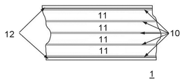
- FIG. 1 shows an example of arrangement of a data band and a servo band.
- a plurality of servo bands 10 are arranged on the magnetic layer of the magnetic tape 1 so as to be sandwiched between guard bands (Guard Band) 12.
- the servo pattern is a magnetization region, which is formed by magnetizing a specific region of the magnetic layer with a servo light head.
- the region magnetized by the servo light head (the position where the servo pattern is formed) is defined by the standard.
- LTO Linear Tape-Open
- a plurality of servo patterns inclined with respect to the tape width direction are formed on the servo band at the time of manufacturing a magnetic tape.
- the servo frame SF on the servo band 10 is composed of a servo subframe 1 (SSF1) and a servo subframe 2 (SSF2).
- the servo subframe 1 is composed of an A burst (reference numeral A in FIG. 2) and a B burst (reference numeral B in FIG. 2).
- the A burst is composed of servo patterns A1 to A5, and the B burst is composed of servo patterns B1 to B5.
- the servo subframe 2 is composed of a C burst (reference numeral C in FIG. 2) and a D burst (reference numeral D in FIG. 2).
- the C burst is composed of servo patterns C1 to C4, and the D burst is composed of servo patterns D1 to D4.
- Such 18 servo patterns are arranged in a set of 5 and 4 in a servo subframe arranged in an array of 5, 5, 4, 4, and used to identify the servo frame.
- FIG. 2 shows one servo frame. However, a plurality of servo frames are arranged in the traveling direction in each servo band.
- the arrow indicates the traveling direction of the magnetic tape. The direction of travel of the arrow is the upstream side, and the opposite side is the downstream side.
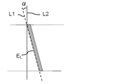
- 3 and 4 are explanatory views of the azimuth angle ⁇ .
- a servo pattern that is inclined toward the upstream side in the traveling direction such as servo patterns A1 to A5 and C1 to C4, two end portions of the edge EL on the downstream side are connected.
- the angle formed by the line segment (broken line L1 in FIG. 3) and the tape width direction (broken line L2 in FIG. 3) is the azimuth angle ⁇ .
- a line segment connecting two ends of the edge EL on the downstream side in FIG. 4
- the angle formed by the broken line L1) and the tape width direction is the azimuth angle ⁇ .
- the magnetic recording head that forms a servo pattern on the magnetic layer of the magnetic recording medium is the servo light head.
- FIG. 5 shows an example of arrangement of the light gap in the magnetic recording head (servo light head) for forming the servo pattern as described above.
- FIG. 5 is a schematic plan view of the magnetic film observed from the recording surface side of the magnetic recording head, and is provided with five pairs of “/ ⁇ ” light gaps in the longitudinal direction L. Therefore, the magnetic film M of the magnetic recording head is provided with a total of 10 light gaps WG (white portions in the figure). Each light gap is inclined with respect to the longitudinal direction at the same azimuth angle ⁇ as the servo pattern to be formed on the magnetic layer of the magnetic recording medium.
- a pulse current is applied to the magnetic recording head facing the magnetic layer surface of the magnetic recording medium to be recorded in contact or non-contact state to generate a leakage magnetic field between the light gaps at a position where a predetermined servo pattern should be formed.
- a servo pattern can be formed on each of the five servo bands in the arrangement shown in FIG.
- a pair of servo patterns (servo pattern A1 and servo pattern B1) can be formed by a pair of light gaps of "/ ⁇ ", and the servo patterns A2, servo pattern B2, and servo can be sequentially formed.
- FIGS. 6A and 6B are explanatory views of the measurement position of the gap width.
- the measurement direction of the gap width is a direction orthogonal to the azimuth angle direction.
- the dotted arrow indicates the azimuth angle direction
- the solid arrow indicates the measurement direction of the gap width.
- FIG. 6A shows a light gap for forming A-burst and C-burst servo patterns.
- FIG. 6B shows a light gap for forming B-burst and D-burst servo patterns.
- a magnetic recording head for forming a servo pattern on the magnetic layer of a magnetic recording medium applicable to a timing-based servo system
- the magnetic recording head is not limited to the one for forming a timing-based servo pattern, and may be for forming a servo pattern that enables head tracking in, for example, an amplitude-based servo method.
- timing-based servo head tracking see, for example, known techniques such as those described in U.S. Pat. Nos. 5,689,384, U.S. Pat. No. 6,542,325 and U.S. Pat. No. 7,876,521.
- the magnetic recording head can also be used as a magnetic recording head for data recording.
- the magnetic recording head can also be used as a magnetic recording head for recording various information (data) on a magnetic layer on which a servo pattern is already formed on a magnetic recording medium.
- ion beam processing refers to a process of forming an opening by irradiating an ion beam.
- the opening formed in this way has a form of a through hole penetrating from the surface of the magnetic film on the recording surface side to the surface of the back surface side, and an opening on the front surface side portion of the magnetic film on the recording surface side and the back surface side.
- the surface of the is included in a non-penetrating form.
- the opening formed by irradiating the magnetic film with an ion beam and processing the ion beam is a physically open portion.
- the opening width becomes narrower in the thickness direction from the surface of the magnetic film on the recording surface side.
- a portion that has been altered by ion irradiation can be confirmed in the vicinity of the opening. This is because the processing target area for ion beam processing is usually designated by a scanning ion microscope (SIM) image.
- SIM scanning ion microscope
- the opening formed in the magnetic film by ion beam processing has a feature that the opening width becomes narrower in the thickness direction from the surface of the magnetic film on the recording surface side. Therefore, in the light gap produced by simply processing the magnetic film with an ion beam, the gap width on the recording surface side is wider than the gap width on the back surface side. On the recording surface side where the gap width is wide, the magnetic resistance becomes large, which makes it difficult for the magnetic flux to be focused. This is considered to be a cause of reducing the recording ability of the magnetic recording head.
- the present inventor for example, by adopting a manufacturing method as described later, has an opening formed by ion beam processing at the gap end on the recording surface side while having an opening.
- magnetism means ferromagnetic property
- non-magnetic means not ferromagnetism.
- the magnetism soft magnetism is preferable, and for non-magnetism, it is preferable that the relative magnetic permeability is sufficiently close to 1.0 as compared with a general high magnetic permeability material.
- the recording surface side gap width of the write gap calculated as the arithmetic mean of the measured values in all the recording surface side narrow light gaps included in the magnetic recording head shall be, for example, 0.1 ⁇ m or more.
- the thickness is preferably 0.2 ⁇ m or more, and more preferably 0.5 ⁇ m or more.
- the gap width on the recording surface side of the write gap can be, for example, 2.0 ⁇ m or less, and from the viewpoint of further improving the recording ability, it is preferably 1.5 ⁇ m or less, preferably 1.3 ⁇ m or less. It is more preferable to have.
- the recording surface side gap width obtained as the arithmetic mean of the measured values at the three points as described above may also be within the above range. It is possible, and it is preferable that it is in the above range.
- the backside gap width of the light gap calculated as the arithmetic mean of the measured values in all the recording surface side narrow light gaps included in the magnetic recording head is, for example. It can be 1.0 ⁇ m or more, and from the viewpoint of further improving the recording ability, it is preferably 2.0 ⁇ m or more, and more preferably 5.0 ⁇ m or more. Further, the gap width on the back surface side of the light gap can be, for example, 25.0 ⁇ m or less, and is preferably 20.0 ⁇ m or less, preferably 15.0 ⁇ m or less, from the viewpoint of further improving the recording ability. Is more preferable.
- the back surface side gap width obtained as the arithmetic mean of the measured values at the three points can also be within the above range as described above. , The above range is preferable.
- the backside gap width of the light gap calculated as the arithmetic average of the measured values in all the recording surface side narrow light gaps and the measured values in all the recording surface side narrow light gaps can be more than 1.0, preferably 1.5 or more. , 2.0 or more is more preferable, and 5.0 or more is further preferable.
- the above ratio can be, for example, 60.0 or less, preferably 50.0 or less, more preferably 40.0 or less, still more preferably 30.0 or less. It is more preferably 20.0 or less.
- the ratio between the back surface side gap width and the recording surface side gap width obtained as the arithmetic mean of the measured values at the three points as described above. (Back side gap width / recording surface side gap width) can also be in the above range, and is preferably in the above range.
- At least one light gap preferably all light gaps, are narrow light gaps on the recording surface side, and an opening formed by ion beam processing is formed at the gap end on the recording surface side.
- ion beam processing for example, as described in US Pat. No. 6,269,533 (Patent Document 1), a delicate gap can be formed, but simply by ion beam processing, as described above.
- the recording ability is lowered because the gap width on the recording surface side becomes wider than the gap width on the back surface side.
- the magnetic recording head has an opening formed by ion beam processing at the gap end on the recording surface side, but is high because the gap width on the recording surface side includes a light gap narrower than the gap width on the back surface side. You can demonstrate your recording ability. Details of the method for forming such a light gap will be described later.
- the magnetic recording head can be a ring-type magnetic recording head and can be an inductive head.
- the inductive head is also generally referred to as an electromagnetic induction type head or a magnetic induction type head.
- the inductive head causes a leakage magnetic field to be generated from the light gap of the head core by passing a current through the coil, and the leakage magnetic field can form a magnetized region in the magnetic layer of the magnetic recording medium.
- FIG. 7 is a perspective view showing an example of the magnetic recording head.
- FIG. 7 is a perspective view of the magnetic recording head observed from the recording surface side.
- the magnetic recording head 20 shown in FIG. 7 has a head block 21, a shield case 22, and a coil 25 (see FIG. 8).
- the shield case 22 is a case for shielding the magnetic field generated from the coil 25 (see FIG. 8) of the magnetic recording head 20 and / or shielding the magnetic field from other external parts.
- the shield case 22 can be a rectangular parallelepiped case having a hollow inside, which is formed of a known material capable of shielding a magnetic field.
- An opening 24 for exposing the head block 21 from the shield case 22 is provided in the upper part of the shield case 22. Further, an opening is provided in the lower part of the shield case 22 for pulling out the conducting wire 23 connected to the coil 25 to the outside of the shield case 22.
- FIG. 8 is a cross-sectional view of the magnetic recording head 20 shown in FIG. 7.
- the cross-sectional view shown in FIG. 8 is a cross-sectional view in the width direction W which is a direction orthogonal to the longitudinal direction L of the magnetic recording head 20.
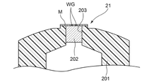
- the head block 21 has a core portion 201 and a substrate 202 having a magnetic film M on the core portion 201.
- the core portion 201 is excited by the coil 25, the light gap of the magnetic film hinders the magnetic flux that tries to pass through the magnetic film. As a result, a leakage magnetic field is generated at the position of the light gap. By this leakage magnetic field, a magnetized region can be formed in the magnetic layer of the magnetic recording medium, that is, recording can be performed.
- a magnetic material usually used for the core portion of the ring-type magnetic recording head can be used.
- the magnetic material include ferrites such as single crystal ferrite and polycrystalline ferrite, and examples of the ferrite include manganese-zinc ferrite.
- An opening 203 that penetrates in the vertical direction along the longitudinal direction is formed in the vicinity of the center in the width direction in the upper part of the core portion 201.
- the substrate 202 is arranged in the opening 203 so as to fill the opening 203.
- Examples of the material of the substrate 202 include non-magnetic materials (for example, various glass materials and various ceramic materials).
- FIG. 9 is a partially enlarged view of a cross-sectional view of the magnetic recording head 20 shown in FIG.
- the magnetic film M provided on the substrate 202 is provided with a light gap WG.
- the magnetic film M can be a metal film.
- the "metal film” includes an alloy film.
- the metal film can be a deposited film on which one or more metal materials selected from the group consisting of one or more pure metals and one or more alloys are deposited and may contain one or more additives. It can and / or may contain one or more impurities that are inevitably contaminated.
- the magnetic film M can be an iron-based alloy film.
- “system” means "includes”.
- the iron-based alloy film can preferably be an iron nitride-based alloy film. Examples of the iron nitride based alloy include those containing one or more selected from the group consisting of Al, Ta, etc. together with Fe and N as constituent elements.
- a metal material was deposited on the substrate by a known film forming method such as physical vapor deposition (PVD) such as sputtering and vacuum deposition, and chemical vapor deposition (CVD). It can be a deposition film.
- PVD physical vapor deposition
- CVD chemical vapor deposition
- the thickness of the magnetic film M can be, for example, 0.5 ⁇ m or more, preferably 1.0 ⁇ m or more, and more preferably 3.0 ⁇ m or more from the viewpoint of further improving the recording ability.
- the thickness of the magnetic layer M can be, for example, 12.0 ⁇ m or less, preferably 10.0 ⁇ m or less, and 8.0 ⁇ m or less, from the viewpoint of ease of forming a magnetic film having a uniform film quality. It is more preferable to have.
- the thickness of the magnetic film shall be the thickness at one randomly selected part of the magnetic film of the magnetic recording head that does not have a light gap. Such a thickness can be measured in a cross-sectional sample of a portion including a magnetic film by preparing a cross-sectional sample. For specific examples of the method for preparing the cross-section sample, the above description can be referred to. The measurement can be performed by a known measuring device having a length measuring function such as SEM.
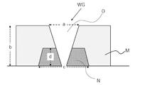
- FIGS. 10A and 10B are enlarged views (cross-sectional views) of a portion of the magnetic film having a light gap.
- FIGS. 10A and 10B will be collectively referred to as “FIG. 10”.
- the magnetic film M has a light gap WG, “a” indicates the recording surface side gap width, “b” indicates the magnetic film thickness, and “c” indicates the back surface side gap width.
- the light gap WG has an opening O formed by ion beam processing at the gap end on the recording surface side. It is preferable that the opening formed by ion beam processing physically opens at least on the recording surface side in the narrow light gap on the recording surface side of the magnetic recording head and penetrates the magnetic film.
- FIG. 10 shows an example in which the opening O penetrates the back surface side. However, the opening formed by ion beam processing does not have to penetrate the back surface side in the narrow light gap on the recording surface side of the magnetic recording head. This is because, as will be described later, the non-magnetic material portion can provide a magnetic spacing.
- the light gap WG shown in FIG. 10A has a non-magnetic material portion N at the gap end on the back surface side.
- one layer of the non-magnetic material portion is provided.
- the light gap WG shown in FIG. 10B is provided with two layers of non-magnetic material portions (non-magnetic material portions N1 and N2).
- the cross-sectional shape of the non-magnetic material portion is trapezoidal.
- the cross-sectional shape of the non-magnetic material portion is not limited to this, and may be any shape such as an arc, a square, a rectangle, and a multi-stage structure.
- non-magnetic material constituting the non-magnetic material portion examples include non-magnetic oxides such as silicon oxide (for example, SiO 2 ) and titanium acid compounds (for example, CaTIO 3 and BaTiO 3 ), aluminum, and copper.
- non-magnetic oxides such as silicon oxide (for example, SiO 2 ) and titanium acid compounds (for example, CaTIO 3 and BaTiO 3 ), aluminum, and copper.
- a material having a thermal expansion coefficient close to that of the material constituting the core portion is preferable.
- ferrite can be mentioned as a material constituting the core portion, and from the viewpoint that the coefficient of thermal expansion is close to that of ferrite, non-magnetic oxide is used as the non-magnetic material constituting the non-magnetic material portion.
- silicon oxide is more preferred.
- the non-magnetic material part is a deposited film in which a non-magnetic material is deposited on a substrate by a known film forming method such as physical vapor deposition (PVD) such as sputtering or vacuum deposition, or chemical vapor deposition (CVD). Can be done.
- PVD physical vapor deposition
- CVD chemical vapor deposition
- the non-magnetic materials constituting the non-magnetic material parts may be the same or different.
- the thickness of the non-magnetic material portion (reference numeral “d” in FIG. 10) is, for example, 3% or more with respect to the thickness of the magnetic film (reference numeral b in FIG. 10, that is, assuming that the thickness of the magnetic film is 100%). From the viewpoint of further improving the recording ability, it is preferably 5% or more, more preferably 10% or more, and further preferably 20% or more.
- the thickness of the non-magnetic material portion can be, for example, 95% or less with respect to the thickness of the magnetic film, and is preferably 90% or less, preferably 80% or less, from the viewpoint of further improving the recording ability. It is more preferably present, and further preferably 70% or less.
- the thickness of the non-magnetic material portion is the total thickness of the two or more non-magnetic material portions.
- the thickness of the non-magnetic material portion can be, for example, 0.1 ⁇ m or more, preferably 0.3 ⁇ m or more, more preferably 0.5 ⁇ m or more, and 10.0 ⁇ m or less. It is possible, preferably 9.0 ⁇ m or less, and more preferably 8.0 ⁇ m or less.
- At least one light gap is a narrow light gap on the recording surface side.
- the thickness of the non-magnetic material portion of the narrow light gap on the recording surface side described for the magnetic recording head is the non-magnetic material portion of all the narrow light gaps on the recording surface side having the non-magnetic material portion included in the magnetic recording head.
- Such an arithmetic mean can be in the above range, preferably in the above range.
- the measurement of the thickness of the non-magnetic material portion for obtaining the arithmetic mean in each recording surface side narrow light gap having the non-magnetic material portion shall be performed at one randomly selected place of the non-magnetic material portion.
- the thickness of the non-magnetic material portion can be measured by preparing a cross-sectional sample of the portion including the non-magnetic material portion and measuring the cross-sectional sample. The measurement can be performed by a known measuring device having a length measuring function such as SEM. Further, the thickness of the non-magnetic material portion of each recording surface side narrow light gap having the non-magnetic material portion can also be in the above range, and is preferably in the above range.
- the opening formed by ion beam processing penetrates the non-magnetic material portion. Therefore, there is also an opening formed by ion beam processing at the gap end on the back surface side.
- the gap width means the width of the magnetic spacing
- the gap width on the back surface side is the width of the non-magnetic material portion (reference numeral “c” in FIG. 10).
- the magnetic recording head is not limited to the form in which the opening formed by ion beam processing penetrates the non-magnetic material portion, and is not present in at least a part including the gap end portion on the back surface side.
- the magnetic material portion may include a solid portion having no physical opening.
- a magnetic recording head having a narrow light gap on the recording surface side including the non-magnetic material portion as described above can be manufactured, for example, by the manufacturing method described below.
- the magnetic recording head has a non-magnetic material portion formed on a substrate, a magnetic film formed on the substrate so as to cover the non-magnetic material portion, and a portion where a light gap of the magnetic film should be formed. It can be manufactured by a manufacturing method including forming an opening by ion beam processing. The ion beam processed portion has the non-magnetic material portion between the magnetic film and the substrate. According to such a manufacturing method, a magnetic recording head having a light gap having an opening formed by ion beam processing at the gap end on the recording surface side and a non-magnetic material portion at the gap end on the back surface side is manufactured. be able to.
- FIG. 11 shows an explanatory diagram of the method for forming the light gap shown in FIG. 10A.
- FIG. 11 shows an explanatory diagram of the method for forming the light gap shown in FIG. 10A.
- an example of the above manufacturing method will be described with reference to FIG.
- the above manufacturing method is not limited to the form shown in FIG.
- the non-magnetic material portion N is formed on the substrate 202 arranged in the opening 203 of the core portion 201 (FIG. 11A).
- a method of forming the non-magnetic material portion N on the substrate 202 after forming a continuous layer of the non-magnetic material on the substrate 202, a non-magnetic material is used as a pattern of the non-magnetic material by a known patterning method such as a lithography process. A method of forming the portion N can be mentioned.
- the non-magnetic material and the thickness constituting the non-magnetic material portion are as described above.
- the above-mentioned description regarding the non-magnetic material portion of the light gap can be referred to. Since the width of the non-magnetic material portion N (pattern) is the back side gap width of the formed light gap, the back side gap width can be controlled by adjusting the size of the pattern.
- the pattern of the formed non-magnetic material is placed on the pattern.
- a method of forming a second layer of non-magnetic material in a pattern can be adopted.
- patterning may be performed after laminating and forming two continuous layers of non-magnetic materials.
- a magnetic film M is formed on the substrate 202 so as to cover the non-magnetic material portion N (FIG. 11 (b)).
- the thickness of the magnetic film and the film forming method are as described above.
- a magnetic film is formed on the surface of the core portion 201 in addition to the substrate 202.
- the magnetic film M can be provided on the recording surface side of the core portion 201.
- ion beam IB (Ion Beam) is irradiated toward the surface of the magnetic film on the recording surface side to perform ion beam processing (FIG. 11 (c)).
- ion beam IB Ion Beam
- FIG. 11 (c) ion Beam
- the opening formed in this way becomes narrower in the depth direction due to the characteristics of ion beam processing.
- the width of the pattern of the non-magnetic material portion N is made larger than the opening width of the opening formed on the recording surface side by ion beam processing for recording. It is possible to form a light gap in which the front side gap width is narrower than the back side gap width.
- Ion beam processing can be performed by known ion beam processing that can form an opening by irradiating the processing target with an ion beam.
- Ion beam processing can be performed by processing generally called ion milling, and from the viewpoint of processing accuracy and the like, focused ion beam (FIB) processing is preferable.
- the ion beam is a beam in which ions are accelerated by an electric field
- the focused ion beam is an ion beam in which an ion beam is focused by a lens or the like.
- Focused ion beam processing is also commonly referred to as FIB processing. Focused ion beam processing can be performed using a commercially available or known focused ion beam device.
- the processing conditions may be set according to the type of material to be processed, the film thickness, and the like.
- Magnetic recording device One aspect of the present invention relates to a magnetic recording device including the magnetic recording head.
- a servo writer is a magnetic recording device that has a servo light head and forms a servo pattern on the magnetic layer of a magnetic recording medium by the servo light head.
- the magnetic recording device can be a servo lighter in one form.
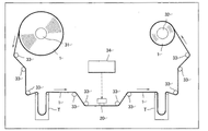
- FIG. 12 is a schematic diagram showing the configuration of the servo lighter.
- the servo writer 30 shown in FIG. 12 has a reel 31 for sending out the magnetic tape 1 before forming the servo pattern, and a reel 32 for winding up the magnetic tape 1 on which the servo pattern is formed.
- the arrows in FIG. 12 indicate the transport direction of the magnetic tape 1.
- a plurality of guides 33 and a tension adjusting device T for adjusting the tension of the magnetic tape 1 to be conveyed are arranged in the conveying path of the magnetic tape 1.
- the magnetic recording head (servo light head) 20 forms a servo pattern on the magnetic layer of the magnetic tape 1 to be conveyed.
- the write signal generation circuit 34 transmits a pulse signal for forming a servo pattern to the magnetic recording head (servo light head) 20.
- a leakage magnetic field is generated from the light gap WG of the magnetic recording head (servo light head) 20, and the leakage magnetic field can form a magnetization region (servo pattern) in the magnetic layer of the magnetic recording medium.
- One aspect of the present invention relates to a method for manufacturing a magnetic recording medium having a servo pattern, which comprises forming a servo pattern on the magnetic recording medium by the magnetic recording head.
- the servo lighter shown in FIG. 12 can be used. However, it is not limited to this.
- the formed servo pattern can be a timing-based servo pattern in one form.
- the timing-based servo method is adopted in the magnetic tape (generally called "LTO tape") compliant with the LTO (Linear Tape-Open) standard. ing.
- the servo pattern is composed of a pair of magnetic stripes (also referred to as "servo stripes") that are non-parallel to each other and are continuously arranged in a plurality in the longitudinal direction of the magnetic tape.
- the reason why the servo pattern is composed of a pair of magnetic stripes that are non-parallel to each other is to teach the passing position to the servo signal reading element passing on the servo pattern.
- the pair of magnetic stripes described above are formed so that their spacing changes continuously along the width direction of the magnetic tape, and the servo signal reading element reads the spacing to obtain a servo pattern.
- the relative position of the servo signal reading element can be known. This relative position information allows tracking of the data track. Therefore, a plurality of servo tracks are usually set on the servo pattern along the width direction of the magnetic tape.
- the servo band is composed of a servo pattern that is continuous in the longitudinal direction of the magnetic tape.
- a plurality of these servo bands are usually provided on the magnetic tape. For example, in LTO tape, the number is five.
- the area sandwiched between two adjacent servo bands is the data band.
- the data band is composed of a plurality of data tracks, and each data track corresponds to each servo track.
- each servo band has information indicating the number of the servo band (“servo band ID (identification)” or “UDIM (Unique DataBand Identification)”. Also called "Servo) information”) is embedded.
- the servo band ID is recorded by shifting a specific pair of servo stripes in the servo band so that their positions are relatively displaced in the longitudinal direction of the magnetic tape. Specifically, the method of shifting a specific pair of servo stripes is changed for each servo band. As a result, the recorded servo band ID becomes unique for each servo band, so that the servo band can be uniquely identified by simply reading one servo band with the servo signal reading element.
- a method for uniquely specifying the servo band there is also a method using a staggered method as shown in ECMA-319 (June 2001).
- a staggered method a group of a pair of magnetic stripes (servo stripes) that are continuously arranged in the longitudinal direction of the magnetic tape and are non-parallel to each other are recorded so as to be shifted in the longitudinal direction of the magnetic tape for each servo band. do. Since this combination of shifting methods between adjacent servo bands is unique in the entire magnetic tape, it is possible to uniquely identify the servo band when reading the servo pattern by the two servo signal reading elements. It is possible.
- LPOS Longitorial Position
- the embedded information may be different for each servo band such as UDIM information, or may be common to all servo bands such as LPOS information.
- a method of embedding information in the servo band a method other than the above can be adopted. For example, a predetermined code may be recorded by thinning out a predetermined pair from a group of a pair of servo stripes.
- the magnetic tape is usually demagnetized (erase).
- This erasing process can be performed by applying a uniform magnetic field to the magnetic tape using a DC magnet or an AC magnet.
- the erase processing includes DC (Direct Current) erase and AC (Alternating Current) erase.
- AC erase is performed by gradually reducing the strength of the magnetic field while reversing the direction of the magnetic field applied to the magnetic tape.
- DC erase is performed by applying a unidirectional magnetic field to the magnetic tape.
- the first method is horizontal DC erase, which applies a unidirectional magnetic field along the longitudinal direction of the magnetic tape.
- the second method is vertical DC erase, which applies a unidirectional magnetic field along the thickness direction of the magnetic tape.
- the erasing process may be performed on the entire magnetic tape or may be performed on each servo band of the magnetic tape.
- the direction of the magnetic field of the formed servo pattern is determined by the direction of erase. For example, when the magnetic tape is horizontally DC erased, the servo pattern is formed so that the direction of the magnetic field is opposite to the direction of the erase. As a result, the output of the servo signal obtained by reading the servo pattern can be increased.
- Japanese Patent Application Laid-Open No. 2012-53940 when a magnetic pattern using the above gap is transferred to a vertically DC-erased magnetic tape, the formed servo pattern is read and obtained.
- the servo signal has a unipolar pulse shape.
- the servo signal obtained by reading the formed servo pattern has a bipolar pulse shape.
- the magnetic recording medium includes a tape-shaped magnetic recording medium (that is, a magnetic tape) and a disk-shaped magnetic tape (that is, a magnetic disk). Further, the magnetic recording medium is generally roughly classified into a coating type and a metal thin film type.
- the magnetic recording medium on which the servo pattern is formed by the magnetic recording head can be a magnetic tape or a magnetic disk, and is preferably a magnetic tape. Further, the magnetic recording medium may be a coating type magnetic recording medium or a metal thin film type magnetic recording medium.
- the magnetic recording medium usually has a non-magnetic support and a magnetic layer containing a ferromagnetic powder, and can have a non-magnetic layer containing a non-magnetic powder between the non-magnetic support and the magnetic layer, and is non-magnetic. It is also possible to have a backcoat layer containing non-magnetic powder on the surface side opposite to the surface side having the magnetic layer of the magnetic support.
- the magnetic layer, the non-magnetic layer and the backcoat layer include a binder and can optionally contain one or more kinds of additives.
- the metal thin film type magnetic recording medium can have, for example, a magnetic layer formed by a sputtering method.
- the magnetic recording head Since the magnetic recording head has a light gap including an opening formed by ion beam processing and can exhibit high recording ability, it is necessary to record on the magnetic layer of a magnetic recording medium having a high coercive force. It is suitable as a magnetic recording head. Regarding the coercive force of the magnetic recording medium, the magnetic recording head is suitable as, for example, a magnetic recording head for recording on the magnetic layer of the magnetic recording medium having a vertical coercive force of 2800 Oe or more. The magnetic recording head is more preferably suitable for recording on a magnetic layer of a magnetic recording medium having a vertical coercive force of 3000 Oe or more, and also for recording on a magnetic recording medium of a magnetic recording medium having a vertical coercive force of 3500 Oe or more.
- the vertical coercive force of the magnetic recording medium can be, for example, 5000 Oe or less. However, this may be exceeded.
- the magnetic recording head can also be applied to recording on a magnetic layer of a magnetic recording medium having a low coercive force.
- 1 Oe (1 oersted) 79.6 A / m.
- the "vertical coercive force" of the magnetic recording medium is the coercive force measured in the vertical direction of the magnetic recording medium.
- the "vertical direction” described with respect to the coercive force is a direction orthogonal to the surface of the magnetic layer, and can also be referred to as a thickness direction.
- the vertical coercive force of the magnetic recording medium is a value obtained by the following method using a vibrating sample magnetometer. A sample piece of a size that can be introduced into a vibration sample magnetometer is cut out from the magnetic recording medium to be measured.
- the vibrating sample magnetometer uses a vibrating sample magnetometer to apply a magnetic field in the vertical direction of the sample piece (direction orthogonal to the surface of the magnetic layer) at a maximum applied magnetic field of 3979 kA / m, a measured temperature of 296 K, and a magnetic field sweep speed of 8.3 kA / m / sec. It is applied and the magnetization strength of the sample piece with respect to the applied magnetic field is measured.
- the measured value shall be obtained as the value obtained by subtracting the magnetization of the sample probe of the vibrating sample magnetometer as background noise.
- the coercive force (vertical coercive force) is obtained from the applied magnetic field at which the magnetization strength becomes zero.
- the measurement temperature is the temperature of the sample piece. By setting the ambient temperature around the sample piece to 296K, the temperature of the sample piece can be set to 296K (measurement temperature) by establishing a temperature equilibrium.
- Examples of the ferromagnetic powder contained in the magnetic layer of the magnetic recording medium include hexagonal ferrite powder and ⁇ -iron oxide powder.
- the "hexagonal ferrite powder” refers to a ferromagnetic powder in which a hexagonal ferrite type crystal structure is detected as the main phase by X-ray diffraction analysis.
- the main phase refers to a structure to which the highest intensity diffraction peak belongs in the X-ray diffraction spectrum obtained by X-ray diffraction analysis. For example, when the highest intensity diffraction peak is attributed to the hexagonal ferrite type crystal structure in the X-ray diffraction spectrum obtained by X-ray diffraction analysis, it is determined that the hexagonal ferrite type crystal structure is detected as the main phase. It shall be.
- the hexagonal ferrite type crystal structure contains at least iron atoms, divalent metal atoms and oxygen atoms as constituent atoms.
- the divalent metal atom is a metal atom that can be a divalent cation as an ion, and examples thereof include an alkaline earth metal atom such as a strontium atom, a barium atom, and a calcium atom, and a lead atom.
- the "hexagonal strontium ferrite powder” means that the main divalent metal atom contained in this powder is a strontium atom, and the "hexagonal barium ferrite powder” means this powder.
- the main divalent metal atom contained in is a barium atom.
- the main divalent metal atom is a divalent metal atom that occupies the largest amount on an atomic% basis among the divalent metal atoms contained in this powder.
- rare earth atoms are not included in the above divalent metal atoms.
- the "rare earth atom” in the present invention and the present specification is selected from the group consisting of a scandium atom (Sc), a yttrium atom (Y), and a lanthanoid atom.
- the lanthanoid atoms are lanthanum atom (La), cerium atom (Ce), placeodium atom (Pr), neodymium atom (Nd), promethium atom (Pm), samarium atom (Sm), uropyum atom (Eu), gadrinium atom (Gd).
- Tb Terbium atom
- Dy dysprosium atom
- Ho formium atom
- Er erbium atom
- Tm thulium atom
- Yb ytterbium atom
- Lu lutethium atom
- ⁇ -iron oxide powder refers to a ferromagnetic powder in which an ⁇ -iron oxide type crystal structure is detected as a main phase by X-ray diffraction analysis.
- X-ray diffraction analysis For example, when the highest intensity diffraction peak is attributed to the ⁇ -iron oxide type crystal structure in the X-ray diffraction spectrum obtained by X-ray diffraction analysis, the ⁇ -iron oxide type crystal structure is detected as the main phase. It shall be judged.
- the ⁇ -iron oxide powder includes a substituted ⁇ -iron oxide powder in which a part of Fe is substituted with a substituted atom such as Ga, Co, Ti, Al, and Rh, and a non-substituted type ⁇ -iron oxide powder containing no such substituted atom.
- ⁇ -Iron oxide powder is included.
- the magnetic recording heads of the examples shown in FIGS. 8, 9 and 10A were produced.
- the material of the core portion 201 is manganese-zinc-based ferrite
- the material of the substrate 202 is silicon oxide.
- a continuous layer of silicon oxide was formed on the substrate 202 by a sputtering method using SiO 2 as a target for sputtering, and then patterned by a lithography process to form a silicon oxide pattern N (FIG. 11 (FIG. 11). a)).
- a magnetic film (a continuous layer of a Ta-containing iron nitride based alloy (Fe content: 80 atomic% or more)) was formed on the substrate 202 by a sputtering method so as to cover the silicon oxide pattern N (FIG. 11 (FIG. 11). b)).
- an image was taken with a scanning ion microscope (SIM) on the magnetic film surface on the recording surface side to obtain a SIM image. A region to be processed is specified using this SIM image, FIB processing is performed in the specified region by a focused ion beam device, and a portion where a light gap of the magnetic film should be formed (a silicon oxide between the magnetic film and the substrate).
- SIM scanning ion microscope
- FIG. 11 (c) An opening was formed in the portion including the pattern N) (FIG. 11 (c)).
- the FIB processing was performed under the following conditions. Focused ion beam device: Hitachi High-Tech FB-2200 Acceleration voltage: 30kV Condensing lens: Yes Aperture diameter: 80 ⁇ m Dwell Time (irradiation time per pixel): 5 ⁇ sec
- Focused ion beam device Hitachi High-Tech FB-2200 Acceleration voltage: 30kV
- Condensing lens Yes
- Aperture diameter 80 ⁇ m
- Dwell Time (irradiation time per pixel) 5 ⁇ sec
- the gap width a on the recording surface side in the light gap can be adjusted by the processing conditions of FIB processing.
- the thickness b of the magnetic film can be adjusted by changing the film forming conditions of the sputtering method. Since the back surface side gap width c corresponds to the width of the silicon oxide pattern formed by patterning, it can be adjusted according to the patterning conditions.
- the thickness d of the non-magnetic material portion can be adjusted by changing the film forming conditions of the sputtering method when forming a continuous layer of silicon oxide. Heads B to N were produced in the same manner as in the production of head A except that one or more of the above were changed.
- the pattern of the silicon oxide of the first layer was performed in the same manner as in the production of the head A, and then the silicon oxide was formed into a pattern on the pattern by the sputtering method, in the same manner as in the production of the head A.
- a head O having the light gap of the example shown in FIG. 10B was produced.
- the head P was manufactured in the same manner as the head A, except that the magnetic film was directly formed on the substrate 202 without forming and patterning the continuous layer of the silicon oxide.
- a plurality of heads A to P were manufactured. Of the plurality of heads, one was used for the various measurements below and the other was used for the recording test below.
- the calculated value is shown in Table 1 as the recording surface side gap width a.
- the arithmetic mean of the measured values obtained by the measurement at 3 points for each light gap was also the value shown in Table 1.
- ⁇ Thickness b of magnetic film> Cross-sectional samples of each of the heads A to P were prepared, and in the prepared cross-sectional samples, the thickness was measured by SEM at one randomly selected portion of the portion of the magnetic film having no light gap under the following conditions. .. The following conditions were also adopted as the measurement conditions using the SEM described later. The measured values are shown in Table 1 as the thickness b of the magnetic film.
- Magnification Select a magnification within the range of 100 to 2000 times that the object to be measured generally fits within the observation field of SEM. Measurement: Measure by comparison with the scale bar displayed on the SEM.
- ⁇ Gap width c on the back side> In each of the heads A to O, for each of the 10 light gaps, the vicinity of the central portion, the vicinity of one end portion (about 10 ⁇ m from the end portion), and the vicinity of the other end portion (from the end portion), respectively.
- a cross-sectional sample is prepared by exposing the cross section in the direction orthogonal to the azimuth angle direction at three points (about 10 ⁇ m), and these cross-sectional samples are used to prepare the end portion on the back surface side in the direction orthogonal to the azimuth angle direction.
- the gap width in that is, the width of the non-magnetic material portion (c in FIG. 10) was measured by SEM.
- the head P for each of the 10 light gaps, the vicinity of the central portion, the vicinity of one end portion (a portion of about 10 ⁇ m from the end portion), and the vicinity of the other end portion (a portion of about 10 ⁇ m from the end portion), respectively.
- the cross section is exposed in the direction orthogonal to the azimuth angle direction to prepare a cross section sample, and using these cross section samples, the gap width at the end portion on the back surface side in the direction orthogonal to the azimuth angle direction ( That is, the opening width at the end portion on the back surface side of the opening formed by FIB processing) was measured by SEM.
- the calculated value is shown in Table 1 as the back surface side gap width c.
- the arithmetic mean of the measured values obtained by the measurement at 3 points for each light gap was also the value shown in Table 1.
- each magnetic recording medium shown in Table 1 is a coating type magnetic tape, which has a non-magnetic layer and a magnetic layer on one surface side of a non-magnetic support in this order, and backs on the other surface side. It has a coat layer.
- the vertical coercive force of the magnetic recording medium in Table 1 is a value obtained by the following method. A sample piece was cut out from each magnetic tape. For this sample piece, a TM-TRVSM5050-SMSL type manufactured by Tamagawa Seisakusho was used as a vibration sample type magnetometer, and the vertical coercive force was determined by the method described above.
- all 10 light gaps are light gaps in which an opening is formed as a through hole in the magnetic film by FIB processing.
- the cross-sectional shape of the through hole formed by the FIB processing of each light gap was a reverse taper shape in which the opening width narrowed from the recording surface side to the back surface side.
- the ten light gaps have an opening formed by FIB processing at the gap end portion on the recording surface side of the light gap. This opening is a through hole that penetrates to the back surface side.
- the cross-sectional shape of the through hole formed by the FIB processing of each light gap was a reverse taper shape in which the opening width narrowed from the recording surface side to the back surface side.
- the gap width on the recording surface side is narrower than the gap width on the back surface side in all of the 10 light gaps.
- the heads A to O could be saturated and recorded on a magnetic tape having a coercive force higher than the coercive force, which was not possible with the head P (comparative test example 1).
- One aspect of the present invention is useful in the technical field of magnetic recording for high-density recording.
Landscapes
- Engineering & Computer Science (AREA)
- Manufacturing & Machinery (AREA)
- Magnetic Heads (AREA)
- Magnetic Record Carriers (AREA)
Abstract
ライトギャップを含む磁性膜を有し、上記ライトギャップにおいて記録面側ギャップ幅は裏面側ギャップ幅より狭くかつ上記ライトギャップの記録面側のギャップ端部にイオンビーム加工により形成された開口部を有する磁気記録ヘッド、上記磁気記録ヘッドを含む磁気記録装置、上記磁気記録ヘッドの製造方法、および磁気記録媒体に上記磁気記録ヘッドによってサーボパターンを形成することを含むサーボパターンを有する磁気記録媒体の製造方法が提供される。
Description
本発明は、磁気記録ヘッドおよびその製造方法、磁気記録装置ならびに磁気記録媒体の製造方法に関する。
磁気記録ヘッドによって磁気記録媒体の磁性層に磁化領域を形成することにより、磁気記録媒体に磁気的に情報を記録することができる。そのような情報の一例としては、サーボ信号が挙げられる。サーボ信号を得るために形成される磁化領域は、サーボパターンと呼ばれる。特許文献1には、サーボパターンの形成に使用される磁気記録ヘッドが開示されている。
特許文献1には、磁気記録媒体に形成すべきサーボパターンの形状に対応した形状のギャップを、集束イオンビームによって形成することが開示されている(特許文献1の請求項1等)。特許文献1の第3欄62行~67行には、集束イオンビームによれば極めて繊細な(extremely precise)ギャップを形成できること等が記載されている。
そこで本発明者は、磁気記録ヘッドの製造工程において、イオンビーム加工によってギャップを形成することを検討した。かかる検討の中で、本発明者は、イオンビーム加工によって形成されたギャップを有する磁気記録ヘッドの記録能力を高めることが望ましいと考えた。これは、以下の理由による。保磁力が高い磁気記録媒体は、熱的安定性に優れるため記録された情報の保持性に優れるものの、記録しづらい傾向がある。したがって、保磁力が高い磁気記録媒体への記録のためには、高い記録能力を有する磁気記録ヘッドが求められる。したがって、高保磁力の磁気記録媒体にも良好に記録を行うためには、磁気記録ヘッドの記録能力が高いことは望ましい。
本発明の一態様は、イオンビーム加工によって形成されたギャップを有し、かつ高い記録能力を発揮することができる磁気記録ヘッドを提供することを目的とする。
本発明の一態様は、
ライトギャップ(write gap)を含む磁性膜を有し、
上記ライトギャップにおいて、記録面側ギャップ幅は裏面側ギャップ幅より狭く、かつ
上記ライトギャップの記録面側のギャップ端部にイオンビーム加工により形成された開口部を有する磁気記録ヘッド、
に関する。
ライトギャップ(write gap)を含む磁性膜を有し、
上記ライトギャップにおいて、記録面側ギャップ幅は裏面側ギャップ幅より狭く、かつ
上記ライトギャップの記録面側のギャップ端部にイオンビーム加工により形成された開口部を有する磁気記録ヘッド、
に関する。
一形態では、上記磁気記録ヘッドは、サーボライト(servo write)ヘッドであることができる。
一形態では、上記ライトギャップの記録面側ギャップ幅は、0.2μm以上1.5μm以下であることができる。
一形態では、上記ライトギャップの裏面側ギャップ幅は、2.0μm以上20.0μm以下であることができる。
一形態では、上記磁性膜の厚みは、1.0μm以上10.0μm以下であることができる。
一形態では、上記ライトギャップは、裏面側のギャップ端部に非磁性材料部を含むことができる。
一形態では、上記記磁性膜の厚みに対して、上記非磁性材料部の厚みは、5%以上90%以下であることができる。
一形態では、上記非磁性材料部を構成する非磁性材料は、ケイ素酸化物であることができる。
一形態では、上記磁性膜は、窒化鉄系合金膜であることができる。
一形態では、上記イオンビーム加工は、集束イオンビーム加工であることができる。
本発明の一態様は、上記磁気記録ヘッドを含む磁気記録装置に関する。
一形態では、上記磁気記録装置は、サーボライター(servo writer)であることができる。
本発明の一態様は、
上記磁気記録ヘッドの製造方法であって、
基板上に非磁性材料部を形成すること、
上記基板上に上記非磁性材料部を覆うように磁性膜を形成すること、
上記磁性膜のライトギャップを形成すべき部分にイオンビーム加工によって開口部を形成すること、
を含み、かつ
上記イオンビーム加工される部分は、上記磁性膜と上記基板との間に上記非磁性材料部を有する製造方法、
に関する。
上記磁気記録ヘッドの製造方法であって、
基板上に非磁性材料部を形成すること、
上記基板上に上記非磁性材料部を覆うように磁性膜を形成すること、
上記磁性膜のライトギャップを形成すべき部分にイオンビーム加工によって開口部を形成すること、
を含み、かつ
上記イオンビーム加工される部分は、上記磁性膜と上記基板との間に上記非磁性材料部を有する製造方法、
に関する。
一形態では、上記イオンビーム加工は、集束イオンビーム加工であることができる。
本発明の一態様は、磁気記録媒体に上記磁気記録ヘッドによってサーボパターンを形成することを含む、サーボパターンを有する磁気記録媒体の製造方法に関する。
一形態では、上記サーボパターンは、タイミングベースサーボパターンであることができる。
一形態では、上記磁気記録媒体の垂直方向保磁力は、2800Oe以上であることができる。
本発明の一態様によれば、イオンビーム加工によって形成されたギャップを有し、かつ高い記録能力を発揮することができる磁気記録ヘッド、この磁気記録ヘッドを含む磁気記録装置、およびこの磁気記録ヘッドの製造方法を提供することができる。また、本発明の一態様によれば、磁気記録媒体に上記磁気記録ヘッドによってサーボパターンを形成することを含む磁気記録媒体の製造方法を提供することができる。
[磁気記録ヘッド]
本発明の一態様は、ライトギャップを含む磁性膜を有し、上記ライトギャップにおいて、記録面側ギャップ幅は裏面側ギャップ幅より狭く、かつ上記ライトギャップの記録面側のギャップ端部にイオンビーム加工により形成された開口部を有する磁気記録ヘッドに関する。
本発明の一態様は、ライトギャップを含む磁性膜を有し、上記ライトギャップにおいて、記録面側ギャップ幅は裏面側ギャップ幅より狭く、かつ上記ライトギャップの記録面側のギャップ端部にイオンビーム加工により形成された開口部を有する磁気記録ヘッドに関する。
本発明および本明細書において、磁気記録ヘッドの磁性膜に含まれる「ライトギャップ」とは、磁気的な間隔であって、記録のための漏れ磁界を発生させる間隔である。かかる磁気的な間隔の幅が、ギャップ幅である。磁気的な間隔には、物理的な間隔、即ち開口部と、物理的には隔たっていないものの非磁性材料が存在することによって磁気的に隔たっている部分と、が包含される。以下に詳述するように、上記磁気記録ヘッドには、イオンビーム加工により形成された開口部を記録面側のギャップ端部に有するライトギャップが含まれる。
本発明および本明細書において、「記録面側」とは、記録時に記録対象の磁気記録媒体の磁性層表面と接触状態または非接触状態で対向する磁気記録ヘッド表面側をいうものとし、かかる表面とは反対の表面側を「裏面側」というものとする。「磁性層(の)表面」とは、磁気記録媒体の磁性層側表面と同義である
本発明および本明細書において、「記録面側ギャップ幅」とは、ライトギャップの記録面側の末端部におけるギャップ幅をいい、「裏面側ギャップ幅」とは、ライトギャップの裏面側の末端部におけるギャップ幅をいう。磁気記録ヘッドには、通常、複数のライトギャップが設けられている。上記磁気記録ヘッドでは、少なくとも1つのライトギャップが、記録面側ギャップ幅が裏面側ギャップ幅より狭く、かつ記録面側のギャップ端部にイオンビーム加工により形成された開口部を有するライトギャップであり、好ましくはすべてのライトギャップが、記録面側ギャップ幅が裏面側ギャップ幅より狭く、かつ記録面側のギャップ端部にイオンビーム加工により形成された開口部を有するライトギャップである。以下において、「記録面側ギャップ幅が裏面側ギャップ幅より狭く、かつ記録面側のギャップ端部にイオンビーム加工により形成された開口部を有するライトギャップ」を、「記録面側幅狭ライトギャップ」と呼ぶ。本発明および本明細書において、「記録面側のギャップ端部」とは、ライトギャップの記録面側の末端部を含む末端部側の部分をいうものとする。「裏面側のギャップ端部」とは、ライトギャップの裏面側の末端部を含む末端部側の部分をいうものとする。各ライトギャップにおいて記録面側ギャップ幅が裏面側ギャップ幅より狭いことは、以下の測定の測定結果に基づき判定される。記録面側および裏面側において、それぞれ3箇所でギャップ幅を測定する。ギャップ幅の測定の詳細は後述する。記録面側および裏面側について、それぞれ測定された値の算術平均を、そのライトギャップの記録面側ギャップ幅および裏面側ギャップ幅として判定を行う。
また、測定対象の磁気記録ヘッドにおける「ライトギャップの記録面側ギャップ幅」とは、1つのライトギャップにおいて3箇所で記録面側ギャップ幅を測定することを、その磁気記録ヘッドが有するすべての記録面側幅狭ライトギャップについて行って得られた値の算術平均として求められる。測定対象の磁気記録ヘッドにおける「ライトギャップの裏面側ギャップ幅」とは、1つのライトギャップにおいて3箇所で裏面側ギャップ幅を測定することを、その磁気記録ヘッドが有するすべての記録面側幅狭ライトギャップについて行って得られた値の算術平均として求められる。
各ライトギャップにおけるギャップ幅の測定箇所は、そのライトギャップの中央部付近と、一方の末端部の近傍(例えば末端部から10μm程度の箇所)と、他方の末端部の近傍(例えば末端部から10μm程度の箇所)と、の3箇所とする。ギャップ幅の測定は、レーザー顕微鏡、走査電子顕微鏡(SEM;Scanning Electron Microscope)等の測長機能を有する公知の測定装置によって行うことができる。測定は、非破壊検査または破壊検査によって行われる。例えば、記録面側ギャップ幅は、磁気記録ヘッドを記録面側から平面視観察することで非破壊に測定することができる。ただし、記録面側ギャップ幅を破壊検査を行って測定することもできる。一方、裏面側ギャップ幅は、通常、破壊検査を行い測定することができる。例えば、ライトギャップを含む部分の断面試料をギャップ幅の測定箇所において作製し、この断面試料において裏面側ギャップ幅を測定することができる。例えば、後述する方向で断面を露出させることによって、ギャップ幅を測定可能な断面試料を作製することができる。断面試料の作製は、公知の方法によって行うことができる。断面試料の作製方法としては、ミクロトーム等を使用して機械的に断面を形成する方法、FIB加工等のイオンビーム加工、レーザー加工等のエネルギーを与えて断面を形成する方法等を挙げることができる。磁気記録ヘッドの材料として通常使用され得る材料の硬度を考慮すると、FIB加工等のイオンビーム加工によって断面試料を作製することが好ましい。また、物理的には隔たっていないものの非磁性材料が存在することによって磁気的に隔たっている部分に関して、非磁性材料によって構成されている部分であるか磁性材料によって構成されている部分であるかは、公知の方法によって、例えば、エネルギー分散型X線分光法、オージェ電子分光法等の元素分析および/または組成分析手法によって、特定できる。
以下に、磁気記録ヘッドによって磁気記録媒体(具体的には磁気テープ)の磁性層に形成される磁化領域の一例であるサーボパターンを形成するための磁気記録ヘッドの一形態について説明する
サーボ信号を利用するヘッドトラッキングを行うシステム(以下、「サーボシステム」と記載する。)としては、近年、タイミングベースサーボ方式のサーボシステムが広く用いられている。タイミングベースサーボ方式のサーボシステム(以下、「タイミングベースサーボシステム」と記載する。)では、2種以上の異なる形状の複数のサーボパターンを磁性層に形成し、サーボ信号読取素子が、異なる形状の2つのサーボパターンを再生した(読み取った)時間間隔と、同種の形状の2つのサーボパターンを再生した時間間隔と、によりサーボ信号読取素子の位置を認識する。本発明および本明細書における「タイミングベースサーボパターン」とは、タイミングベースサーボシステムにおけるヘッドトラッキングが可能なサーボパターンをいう。タイミングベースサーボシステムにおけるヘッドトラッキングが可能なサーボパターンは、サーボパターンを形成するためのヘッドであるサーボライトヘッド(servo write head)により、磁性層に2種以上の異なる形状の複数のサーボパターンとして形成される。一例では、2種以上の異なる形状の複数のサーボパターンが、同種の形状の複数のサーボパターンごとに連続して一定の間隔をもって配置される。他の一例では、異なる種類のサーボパターンが交互に配置される。サーボパターンが同種の形状であることに関しては、サーボパターンの形成において通常生じ得る程度の形状の違いは不問とする。タイミングベースサーボシステムにおけるヘッドトラッキングが可能なサーボパターンの形状およびサーボバンド上での配置は公知であり、具体的形態は後述する。
例えば、現在広く用いられているリニア記録方式では、一般に、タイミングベースサーボシステムが採用されている。かかるシステムに適用される磁気テープには、通常、磁性層に、サーボパターンが形成された領域(「サーボバンド」と呼ばれる)が磁気テープの長手方向に沿って複数存在する。2本のサーボバンドに挟まれた領域は、データバンドと呼ばれる。データ(磁気信号)の記録はデータバンド上で行われ、各データバンドには複数のデータトラックが長手方向に沿って形成される。図1に、データバンドおよびサーボバンドの配置例を示す。図1中、磁気テープ1の磁性層には、複数のサーボバンド10が、ガードバンド(Guard Band)12に挟まれて配置されている。2本のサーボバンドに挟まれた複数の領域11が、データバンドである。サーボパターンは、磁化領域であって、サーボライトヘッドにより磁性層の特定の領域を磁化することによって形成される。サーボライトヘッドにより磁化する領域(サーボパターンを形成する位置)は規格により定められている。例えば業界標準規格であるLTO(Linear Tape-Open)Ultriumフォーマットテープには、磁気テープ製造時に、図2に示すようにテープ幅方向に対して傾斜した複数のサーボパターンが、サーボバンド上に形成される。詳しくは、図2中、サーボバンド10上のサーボフレームSFは、サーボサブフレーム1(SSF1)およびサーボサブフレーム2(SSF2)から構成される。サーボサブフレーム1は、Aバースト(図2中、符号A)およびBバースト(図2中、符号B)から構成される。AバーストはサーボパターンA1~A5から構成され、BバーストはサーボパターンB1~B5から構成される。一方、サーボサブフレーム2は、Cバースト(図2中、符号C)およびDバースト(図2中、符号D)から構成される。CバーストはサーボパターンC1~C4から構成され、DバーストはサーボパターンD1~D4から構成される。このような18本のサーボパターンが5本と4本のセットで、5、5、4、4、の配列で並べられたサーボサブフレームに配置され、サーボフレームを識別するために用いられる。図2には、1つのサーボフレームを示した。ただし、各サーボバンドには、複数のサーボフレームが走行方向に配置される。図2中、矢印は磁気テープの走行方向を示している。矢印の進行方向側が上流側であり、反対側が下流側である。
図3および図4は、アジマス角αの説明図である。図2に示すサーボパターンにおいて、サーボパターンA1~A5、C1~C4のように走行方向の上流側に向けて傾斜しているサーボパターンについては、下流側のエッジELの端部2箇所を結ぶ線分(図3中、破線L1)とテープ幅方向(図3中、破線L2)とのなす角度が、アジマス角αである。一方、サーボパターンB1~B5、D1~D4のように走行方向の下流側に向けて傾斜しているサーボパターンについては、下流側のエッジELの端部2箇所を結ぶ線分(図4中、破線L1)とテープ幅方向(図4中、破線L2)とのなす角度がアジマス角αである。
磁気記録媒体の磁性層にサーボパターンを形成する磁気記録ヘッドが、サーボライトヘッドである。上記のようなサーボパターンを形成するための磁気記録ヘッド(サーボライトヘッド)におけるライトギャップの配置例を図5に示す。図5は、磁気記録ヘッドの記録面側から磁性膜を観察した概略平面図であり、「/\」の一対のライトギャップが、長手方向Lに5対設けられている。したがって、磁気記録ヘッドの磁性膜Mには、合計10本のライトギャップWG(図中の白抜き部)が設けられている。各ライトギャップは、長手方向に対して、磁気記録媒体の磁性層に形成すべきサーボパターンと同じアジマス角αで傾斜している。記録時、記録対象の磁気記録媒体の磁性層表面と接触状態または非接触状態で対向する磁気記録ヘッドにパルス電流を印加して所定のサーボパターンを形成すべき位置でライトギャップ間に漏れ磁界を生じさせることによって、5本のサーボバンド上にそれぞれ、図2に示す配置でサーボパターンを形成することができる。例えば、パルス電流の印加によって、「/ \」の一対のライトギャップにより、一対のサーボパターン(サーボパターンA1とサーボパターンB1)を形成することができ、順次、サーボパターンA2とサーボパターンB2、サーボパターンA3とサーボパターンB3、サーボパターンA4とサーボパターンB4、サーボパターンA5とサーボパターンB5、サーボパターンC1とサーボパターンD1、サーボパターンC2とサーボパターンD2、サーボパターンC3とサーボパターンD3、サーボパターンC4とサーボパターンD4、を形成することができる。こうしてサーボパターン対の形成を繰り返すことによって、複数のサーボフレームSFを順次、磁気記録媒体の磁性層のサーボバンドの長手方向に形成することができる。
図6Aおよび図6Bは、ギャップ幅の測定位置の説明図である。アジマス角αで傾斜しているライトギャップについて、ギャップ幅の測定方向は、アジマス角方向に直交する方向とする。図6Aおよび図6B中、点線矢印はアジマス角方向を示し、実線矢印はギャップ幅の測定方向を示す。記録面側ギャップ幅の測定箇所は、1つのライトギャップについて、先に記載したように3箇所である。裏面側ギャップ幅の測定箇所も、1つのライトギャップについて、先に記載したように3箇所である。図6Aには、AバーストおよびCバーストのサーボパターンを形成するためのライトギャップが示されている。図6Bには、BバーストおよびDバーストのサーボパターンを形成するためのライトギャップが示されている。
上記では、タイミングベースサーボシステムに適用可能な磁気記録媒体の磁性層にサーボパターンを形成するための磁気記録ヘッド(サーボライトヘッド)を例に説明した。ただし、上記磁気記録ヘッドは、タイミングベースサーボパターンを形成するためのものに限定されず、例えば振幅ベースサーボ方式でのヘッドトラッキングを可能とするサーボパターンを形成するためのものであってもよい。 タイミングベースサーボ方式のヘッドトラッキングの詳細については、例えば、米国特許第5689384号、米国特許第6542325号および米国特許第7876521号の各明細書に記載の技術をはじめとする公知技術を参照できる。また、振幅ベースサーボ方式のヘッドトラッキングの詳細については、例えば、米国特許第5426543号および米国特許第5898533号の各明細書をはじめとする公知技術を参照できる。また、一形態では、上記磁気記録ヘッドは、データ記録のための磁気記録ヘッドとして使用することもできる。例えば、磁気記録媒体の既にサーボパターンが形成されている磁性層に各種情報(データ)を記録するための磁気記録ヘッドとして、上記磁気記録ヘッドを使用することもできる。
本発明および本明細書において、「イオンビーム加工」とは、イオンビームを照射することによって開口部を形成する処理をいう。こうして形成される開口部には、磁性膜の記録面側の表面から裏面側の表面に貫通している貫通穴である形態と、磁性膜の記録面側の表面側の部分で開口し裏面側の表面には貫通していない形態と、が包含される。開口部が「イオンビーム加工によって形成された開口部」であることの特定に関して、磁性膜にイオンビームを照射してイオンビーム加工することによって形成された開口部は、物理的に開口した部分、即ち磁性材料も非磁性材料も存在しない部分であって、磁性膜の記録面側の表面から厚み方向に向かって開口幅が狭くなる特徴を有する。また、通常、記録面側の磁性膜表面において、開口部近傍にイオン照射によって変質した部分(所謂焼け跡)を確認できる。これは、通常、イオンビーム加工の加工対象領域を走査イオン顕微鏡(SIM;Scanning Ion Microscpope)像によって指定するからである。
上記の通り、イオンビーム加工によって磁性膜に形成される開口部は、磁性膜の記録面側の表面から厚み方向に向かって開口幅が狭くなる特徴を有する。したがって、単に磁性膜をイオンビーム加工することのみで作製されたライトギャップは、記録面側ギャップ幅が、裏面側ギャップ幅より広くなる。ギャップ幅が広い記録面側では、磁気的抵抗が大きくなるため磁束が集束しづらくなってしまう。このことが、磁気記録ヘッドとしての記録能力を低下させる原因になると考えられる。
これに対し、本発明者は鋭意検討を重ねた結果、例えば後述するような製造方法を採用することによって、記録面側のギャップ端部にイオンビーム加工により形成された開口部を有しつつ、記録面側ギャップ幅が裏面側ギャップ幅より狭い磁気記録ヘッドの提供が可能になることを新たに見出した。かかる磁気記録ヘッドでは、裏面側で発生する磁場が高強度になりやすく、相対的に記録面側に磁束が集束しやすいと考えられる。このことが、記録能力向上に寄与すると推察される。ただし、本発明は、本明細書に記載の推察に限定されるものではない。
これに対し、本発明者は鋭意検討を重ねた結果、例えば後述するような製造方法を採用することによって、記録面側のギャップ端部にイオンビーム加工により形成された開口部を有しつつ、記録面側ギャップ幅が裏面側ギャップ幅より狭い磁気記録ヘッドの提供が可能になることを新たに見出した。かかる磁気記録ヘッドでは、裏面側で発生する磁場が高強度になりやすく、相対的に記録面側に磁束が集束しやすいと考えられる。このことが、記録能力向上に寄与すると推察される。ただし、本発明は、本明細書に記載の推察に限定されるものではない。
本発明および本明細書において、「磁性」とは強磁性(ferromagnetic property)を意味し、「非磁性」とは強磁性ではないことを意味する。磁性としては、軟磁性が好ましく、非磁性については、比透磁率が一般的な高透磁率材料に比べて十分に1.0に近いことが好ましい。
以下、上記磁気記録ヘッドについて、更に詳細に説明する。
<記録面側ギャップ幅、裏面側ギャップ幅>
上記磁気記録ヘッドでは、少なくとも1つのライトギャップが、好ましくはすべてのライトギャップが、記録面側幅狭ライトギャップであり、記録面側ギャップ幅が裏面側ギャップ幅より狭い。
先に記載したように磁気記録ヘッドに含まれるすべての記録面側幅狭ライトギャップでの測定値の算術平均として算出されるライトギャップの記録面側ギャップ幅は、例えば0.1μm以上であることができ、記録能力の更なる向上の観点からは、0.2μm以上であることが好ましく、0.5μm以上であることがより好ましい。また、かかるライトギャップの記録面側ギャップ幅は、例えば2.0μm以下であることができ、記録能力の更なる向上の観点からは、1.5μm以下であることが好ましく、1.3μm以下であることがより好ましい。また、上記磁気記録ヘッドに含まれる各記録面側幅狭ライトギャップについて、先に記載したように3箇所での測定値の算術平均として求められる記録面側ギャップ幅も、上記範囲であることができ、上記範囲であることが好ましい。
一方、上記磁気記録ヘッドにおいて、先に記載したように磁気記録ヘッドに含まれるすべての記録面側幅狭ライトギャップでの測定値の算術平均として算出されるライトギャップの裏面側ギャップ幅は、例えば1.0μm以上であることができ、記録能力の更なる向上の観点からは、2.0μm以上であることが好ましく、5.0μm以上であることがより好ましい。また、かかるライトギャップの裏面側ギャップ幅は、例えば25.0μm以下であることができ、記録能力の更なる向上の観点からは、20.0μm以下であることが好ましく、15.0μm以下であることがより好ましい。また、上記磁気記録ヘッドに含まれる各記録面側幅狭ライトギャップについて、先に記載したように3箇所での測定値の算術平均として求められる裏面側ギャップ幅も、上記範囲であることができ、上記範囲であることが好ましい。
また、先に記載したようにすべての記録面側幅狭ライトギャップでの測定値の算術平均として算出されるライトギャップの裏面側ギャップ幅とすべての記録面側幅狭ライトギャップでの測定値の算術平均として算出されるライトギャップの記録面側ギャップ幅との比(裏面側ギャップ幅/記録面側ギャップ幅)は、1.0超であることができ、1.5以上であることが好ましく、2.0以上であることがより好ましく、5.0以上であることが更に好ましい。また、上記の比は、例えば60.0以下であることができ、50.0以下であることが好ましく、40.0以下であることがより好ましく、30.0以下であることが更に好ましく、20.0以下であることが一層好ましい。また、上記磁気記録ヘッドに含まれる各記録面側幅狭ライトギャップについて、先に記載したように3箇所での測定値の算術平均として求められる裏面側ギャップ幅と記録面側ギャップ幅との比(裏面側ギャップ幅/記録面側ギャップ幅)も、上記範囲であることができ、上記範囲であることが好ましい。
上記磁気記録ヘッドでは、少なくとも1つのライトギャップが、好ましくはすべてのライトギャップが、記録面側幅狭ライトギャップであり、記録面側ギャップ幅が裏面側ギャップ幅より狭い。
先に記載したように磁気記録ヘッドに含まれるすべての記録面側幅狭ライトギャップでの測定値の算術平均として算出されるライトギャップの記録面側ギャップ幅は、例えば0.1μm以上であることができ、記録能力の更なる向上の観点からは、0.2μm以上であることが好ましく、0.5μm以上であることがより好ましい。また、かかるライトギャップの記録面側ギャップ幅は、例えば2.0μm以下であることができ、記録能力の更なる向上の観点からは、1.5μm以下であることが好ましく、1.3μm以下であることがより好ましい。また、上記磁気記録ヘッドに含まれる各記録面側幅狭ライトギャップについて、先に記載したように3箇所での測定値の算術平均として求められる記録面側ギャップ幅も、上記範囲であることができ、上記範囲であることが好ましい。
一方、上記磁気記録ヘッドにおいて、先に記載したように磁気記録ヘッドに含まれるすべての記録面側幅狭ライトギャップでの測定値の算術平均として算出されるライトギャップの裏面側ギャップ幅は、例えば1.0μm以上であることができ、記録能力の更なる向上の観点からは、2.0μm以上であることが好ましく、5.0μm以上であることがより好ましい。また、かかるライトギャップの裏面側ギャップ幅は、例えば25.0μm以下であることができ、記録能力の更なる向上の観点からは、20.0μm以下であることが好ましく、15.0μm以下であることがより好ましい。また、上記磁気記録ヘッドに含まれる各記録面側幅狭ライトギャップについて、先に記載したように3箇所での測定値の算術平均として求められる裏面側ギャップ幅も、上記範囲であることができ、上記範囲であることが好ましい。
また、先に記載したようにすべての記録面側幅狭ライトギャップでの測定値の算術平均として算出されるライトギャップの裏面側ギャップ幅とすべての記録面側幅狭ライトギャップでの測定値の算術平均として算出されるライトギャップの記録面側ギャップ幅との比(裏面側ギャップ幅/記録面側ギャップ幅)は、1.0超であることができ、1.5以上であることが好ましく、2.0以上であることがより好ましく、5.0以上であることが更に好ましい。また、上記の比は、例えば60.0以下であることができ、50.0以下であることが好ましく、40.0以下であることがより好ましく、30.0以下であることが更に好ましく、20.0以下であることが一層好ましい。また、上記磁気記録ヘッドに含まれる各記録面側幅狭ライトギャップについて、先に記載したように3箇所での測定値の算術平均として求められる裏面側ギャップ幅と記録面側ギャップ幅との比(裏面側ギャップ幅/記録面側ギャップ幅)も、上記範囲であることができ、上記範囲であることが好ましい。
<記録面側のギャップ端部>
上記磁気記録ヘッドでは、少なくとも1つのライトギャップが、好ましくはすべてのライトギャップが、記録面側幅狭ライトギャップであって、記録面側のギャップ端部にイオンビーム加工により形成された開口部を有する。イオンビーム加工によれば、例えば米国特許第6269533号明細書(特許文献1)に記載されているように繊細なギャップ形成が可能であるものの、単にイオンビーム加工するのみでは、先に記載したように、記録面側ギャップ幅が裏面側ギャップ幅より広くなるため記録能力は低下してしまうと考えられる。これに対し、上記磁気記録ヘッドは、記録面側のギャップ端部にイオンビーム加工により形成された開口部を有するものの記録面側ギャップ幅が裏面側ギャップ幅より狭いライトギャップを含むことによって、高い記録能力を発揮することができる。そのようなライトギャップを形成するための方法について、詳細は後述する。
上記磁気記録ヘッドでは、少なくとも1つのライトギャップが、好ましくはすべてのライトギャップが、記録面側幅狭ライトギャップであって、記録面側のギャップ端部にイオンビーム加工により形成された開口部を有する。イオンビーム加工によれば、例えば米国特許第6269533号明細書(特許文献1)に記載されているように繊細なギャップ形成が可能であるものの、単にイオンビーム加工するのみでは、先に記載したように、記録面側ギャップ幅が裏面側ギャップ幅より広くなるため記録能力は低下してしまうと考えられる。これに対し、上記磁気記録ヘッドは、記録面側のギャップ端部にイオンビーム加工により形成された開口部を有するものの記録面側ギャップ幅が裏面側ギャップ幅より狭いライトギャップを含むことによって、高い記録能力を発揮することができる。そのようなライトギャップを形成するための方法について、詳細は後述する。
以下、上記磁気記録ヘッドについて、更に詳細に説明する。
<磁気記録ヘッドの構成例>
以下、上記磁気記録ヘッドの構成例を図面を参照して説明する。ただし、図面に示す形態は例示であって、かかる形態に本発明は限定されない。
以下、上記磁気記録ヘッドの構成例を図面を参照して説明する。ただし、図面に示す形態は例示であって、かかる形態に本発明は限定されない。
上記磁気記録ヘッドは、リング型磁気記録ヘッドであることができ、インダクティブヘッドであることができる。インダクティブヘッドは、一般に電磁誘導型ヘッドまたは磁気誘導型ヘッドとも呼ばれる。インダクティブヘッドは、コイルに電流を流してヘッドコアのライトギャップから漏れ磁界を発生させ、この漏れ磁界によって、磁気記録媒体の磁性層に磁化領域を形成することができる。
図7は、上記磁気記録ヘッドの一例を示す斜視図である。図7は、磁気記録ヘッドを記録面側から観察した状態の斜視図である。図7に示す磁気記録ヘッド20は、ヘッドブロック21と、シールドケース22と、コイル25(図8参照)と、を有する。
シールドケース22は、磁気記録ヘッド20が有するコイル25(図8参照)から発生する磁界をシールドし、および/または、外部の他の部品からの磁界をシールドするためのケースである。シールドケース22は、磁界をシールド可能な公知の材料から形成された、内部が中空の直方体形状のケースであることができる。
シールドケース22の上部には、ヘッドブロック21をシールドケース22から露出させるための開口24が設けられている。また、シールドケース22の下部には、コイル25と繋がる導線23をシールドケース22の外部に引き出すための開口が設けられている。
図8は、図7に示す磁気記録ヘッド20の断面図である。図8に示す断面図は、磁気記録ヘッド20の長手方向Lと直交する方向である幅方向Wにおける断面図である。
ヘッドブロック21は、コア部201と、その上に磁性膜Mを有する基板202と、を有する。コイル25によってコア部201が励磁されると、磁性膜のライトギャップが、磁性膜を通過しようとする磁束を妨げる。これにより、ライトギャップの位置で漏れ磁界が発生する。この漏れ磁界によって、磁気記録媒体の磁性層に磁化領域を形成すること、即ち記録を行うことができる。
コア部201を構成する材料としては、リング型磁気記録ヘッドのコア部に通常使用される磁性材料を用いることができる。磁性材料としては、例えば、単結晶フェライト、多結晶フェライト等のフェライトが挙げられ、フェライトとしてはマンガン亜鉛系フェライトを例示できる。コア部201の上部における幅方向の中央近傍には、長手方向に沿って上下方向に貫通する開口203が形成されている。基板202は、この開口203を埋めるように、この開口203内に配置されている。
基板202の材料としては、非磁性材料(例えば各種ガラス材料、各種セラミック材料)が挙げられる。
図9は、図8に示す磁気記録ヘッド20の断面図の一部拡大図である。基板202上に設けられた磁性膜Mには、ライトギャップWGが設けられている。
磁性膜Mは、金属膜であることができる。ここで「金属膜」には、合金膜が包含される。金属膜は、1種以上の純金属および1種以上の合金からなる群から選択される1種以上の金属材料が堆積した堆積膜であることができ、1種以上の添加剤を含むことができ、および/または、不可避的に混入する1種以上の不純物を含み得る。磁性膜Mは、鉄系合金膜であることができる。ここで「系」とは、「含む」を意味する。鉄系合金膜は、好ましくは窒化鉄系合金膜であることができる。窒化鉄系合金としては、構成元素として、FeとNとともにAl、Ta等からなる群から選ばれる1種または2種以上を含むものが挙げられる。磁性膜は、スパッタ、真空蒸着等の物理気相成長(PVD;Physical Vapor Deposition)、化学気相成長(CVD;Chemical Vapor Deposition)等の公知の成膜方法によって基板上に金属材料を堆積させた堆積膜であることができる。
磁性膜Mの厚みは、例えば0.5μm以上であることができ、記録能力の更なる向上の観点からは1.0μm以上であることが好ましく、3.0μm以上であることがより好ましい。また、磁性層Mの厚みは、例えば12.0μm以下であることができ、均質な膜質の磁性膜の形成容易性の観点からは、10.0μm以下であることが好ましく、8.0μm以下であることがより好ましい。
磁性膜の厚みは、磁気記録ヘッドの磁性膜のライトギャップを有さない部分の無作為に選択した1箇所における厚みとする。かかる厚みは、磁性膜を含む部分の断面試料を作製し、この断面試料において測定することができる。断面試料の作製方法の具体例等については、先の記載を参照できる。測定は、SEM等の測長機能を有する公知の測定装置によって行うことができる。
図10Aおよび図10Bは、磁性膜のライトギャップを有する部分の拡大図(断面図)である。以下において、図10Aと図10Bとをまとめて、「図10」と記載する。
図10中、磁性膜MはライトギャップWGを有し、「a」は記録面側ギャップ幅、「b」は磁性膜厚み、「c」は裏面側ギャップ幅を示す。ライトギャップWGは、記録面側のギャップ端部にイオンビーム加工によって形成された開口部Oを有する。イオンビーム加工によって形成された開口部は、上記磁気記録ヘッドが有する記録面側幅狭ライトギャップにおいて、少なくとも記録面側で物理的に開口し、磁性膜を貫通していることが好ましい。図10には、開口部Oが裏面側に貫通している例が示されている。ただし、イオンビーム加工によって形成された開口部は、上記磁気記録ヘッドが有する記録面側幅狭ライトギャップにおいて裏面側に貫通していなくてもよい。後述するように、非磁性材料部によって磁気的な間隔をもたらすことができるからである。
図10Aに示すライトギャップWGは、裏面側のギャップ端部に非磁性材料部Nを有する。図10Aでは、非磁性材料部が1層設けられている。図10Bに示すライトギャップWGには、非磁性材料部が2層(非磁性材料部N1およびN2)設けられている。図10に示す例では、非磁性材料部の断面形状は台形である。ただし、非磁性材料部の断面形状は、これに限定されるものではなく、円弧、正方形、長方形、多段構造等の任意の形状であることができる。
非磁性材料部を構成する非磁性材料としては、ケイ素酸化物(例えばSiO2)、チタン酸化合物(例えばCaTiO3、BaTiO3)等の非磁性酸化物、アルミニウム、銅等を挙げることができる。非磁性材料部を構成する非磁性材料としては、コア部を構成する材料と熱膨張率が近いものが好ましい。先に記載したように、コア部を構成する材料としてはフェライトを挙げることができ、フェライトに熱膨張率が近いという観点から、非磁性材料部を構成する非磁性材料としては非磁性酸化物が好ましく、ケイ素酸化物がより好ましい。
非磁性材料部は、スパッタ、真空蒸着等の物理気相成長(PVD)、化学気相成長(CVD)等の公知の成膜方法によって基板上に非磁性材料を堆積させた堆積膜であることができる。1つのライトギャップに非磁性材料部が2層以上含まれている場合、それら非磁性材料部を構成する非磁性材料は同じであってもよく異なるものでもよい。
非磁性材料部の厚み(図10中、符号「d」)は、磁性膜の厚み(図10中、符号b)に対して、即ち磁性膜の厚みを100%として、例えば3%以上であることができ、記録能力の更なる向上の観点からは、5%以上であることが好ましく、10%以上であることがより好ましく、20%以上であることが更に好ましい。非磁性材料部の厚みは、磁性膜の厚みに対して、例えば95%以下であることができ、記録能力の更なる向上の観点からは、90%以下であることが好ましく、80%以下であることがより好ましく、70%以下であることが更に好ましい。非磁性材料部の厚みは、非磁性材料部の層数が2層以上の場合には、それら2層以上の非磁性材料部の合計厚みとする。また、非磁性材料部の厚みは、例えば0.1μm以上であることができ、0.3μm以上であることが好ましく、0.5μm以上であることがより好ましく、また、10.0μm以下であることができ、9.0μm以下であることが好ましく、8.0μm以下であることがより好ましい。
上記磁気記録ヘッドでは、少なくとも1つのライトギャップが、好ましくはすべてのライトギャップが、記録面側幅狭ライトギャップである。磁気記録ヘッドについて記載する記録面側幅狭ライトギャップの非磁性材料部の厚みとは、その磁気記録ヘッドに含まれる非磁性材料部を有するすべての記録面側幅狭ライトギャップの非磁性材料部の厚みの算術平均とする。かかる算術平均は、上記範囲であることができ、上記範囲であることが好ましい。非磁性材料部を有する各記録面側幅狭ライトギャップにおける算術平均を求めるための非磁性材料部の厚みの測定は、非磁性材料部の無作為に選択した1箇所において行うものとする。非磁性材料部の厚みは、非磁性材料部を含む部分の断面試料を作製し、この断面試料において測定することができる。測定は、SEM等の測長機能を有する公知の測定装置によって行うことができる。また、非磁性材料部を有する各記録面側幅狭ライトギャップの非磁性材料部の厚みも、上記範囲であることができ、上記範囲であることが好ましい。
図10に示す例では、イオンビーム加工によって形成された開口部が非磁性材料部を貫通している。したがって、裏面側のギャップ端部にも、イオンビーム加工によって形成された開口部が存在する。ただし、ギャップ幅は磁気的な間隔の幅を意味するため、裏面側ギャップ幅は、非磁性材料部の幅(図10中、符号「c」)である。また、上記磁気記録ヘッドは、イオンビーム加工によって形成された開口部が非磁性材料部を貫通している形態に限定されず、裏面側のギャップ端部を含む少なくとも一部の部分に存在する非磁性材料部が、物理的な開口部を有さない中実部を含んでもよい。
上記のような非磁性材料部を含む記録面側幅狭ライトギャップを有する磁気記録ヘッドは、例えば、以下に説明する製造方法によって製造することができる。
[磁気記録ヘッドの製造方法]
上記磁気記録ヘッドは、基板上に非磁性材料部を形成すること、上記基板上に上記非磁性材料部を覆うように磁性膜を形成すること、上記磁性膜のライトギャップを形成すべき部分にイオンビーム加工によって開口部を形成すること、を含む製造方法によって製造することができる。上記イオンビーム加工される部分は、上記磁性膜と上記基板との間に上記非磁性材料部を有する。かかる製造方法によれば、記録面側のギャップ端部にイオンビーム加工により形成された開口部を有するとともに裏面側のギャップ端部に非磁性材料部を有するライトギャップを有する磁気記録ヘッドを製造することができる。
上記磁気記録ヘッドは、基板上に非磁性材料部を形成すること、上記基板上に上記非磁性材料部を覆うように磁性膜を形成すること、上記磁性膜のライトギャップを形成すべき部分にイオンビーム加工によって開口部を形成すること、を含む製造方法によって製造することができる。上記イオンビーム加工される部分は、上記磁性膜と上記基板との間に上記非磁性材料部を有する。かかる製造方法によれば、記録面側のギャップ端部にイオンビーム加工により形成された開口部を有するとともに裏面側のギャップ端部に非磁性材料部を有するライトギャップを有する磁気記録ヘッドを製造することができる。
図11に、図10Aに示すライトギャップの形成方法の説明図を示す。以下、図11を参照して上記製造方法の一例について説明する。ただし、上記製造方法は、図11に示す形態に限定されるものではない。
まず、コア部201の開口203内に配置された基板202上に、非磁性材料部Nを形成する(図11(a))。基板202上に非磁性材料部Nを形成する方法としては、基板202上に非磁性材料の連続層を形成した後、リソグラフィプロセス等の公知のパターニング方法によって、非磁性材料のパターンとして非磁性材料部Nを形成する方法を挙げることができる。非磁性材料部を構成する非磁性材料および厚みについては、先に記載した通りである。非磁性材料の連続層の成膜方法については、ライトギャップの非磁性材料部に関する先の記載を参照できる。非磁性材料部N(パターン)の幅が、形成されるライトギャップの裏面側ギャップ幅となるため、パターンのサイズを調整することによって、裏面側ギャップ幅を制御することができる。
図10Bに示す例のように2層以上の非磁性材料部を設ける場合、例えば、1層目の非磁性材料の連続層のパターニングを行った後、形成された非磁性材料のパターンの上に2層目の非磁性材料の層をパターン状に形成する方法を採用できる。または、2層の非磁性材料の連続層を積層形成した後、パターニングを行ってもよい。
次に、基板202上に上記非磁性材料部Nを覆うように磁性膜Mを形成する(図11(b))。磁性膜の厚みおよび成膜方法については先に記載した通りである。ここでは、基板202上に加えて、コア部201の表面にも磁性膜が形成される。これにより、図9に示すように、コア部201の記録面側に磁性膜Mを設けることができる。
その後、磁性膜の記録面側の表面に向かって、イオンビームIB(Ion Beam)を照射してイオンビーム加工を行う(図11(c))。こうして開口部を形成することができる。このように形成される開口部は、イオンビーム加工の特徴から、深さ方向に向かって幅狭になる。ただし、上記のように非磁性材料部を設けているため、非磁性材料部Nのパターンの幅を、イオンビーム加工によって記録面側に形成される開口部の開口幅より大きくすることによって、記録面側ギャップ幅が裏面側ギャップ幅より狭いライトギャップを形成することができる。
イオンビーム加工は、加工対象にイオンビームを照射することによって開口部を形成可能な公知のイオンビーム加工によって行うことができる。イオンビーム加工は、一般にイオンミリング(Ion Milling)と呼ばれる加工によって行うことができ、加工精度等の観点からは集束イオンビーム(FIB;Focused Ion Beam)加工であることが好ましい。イオンビームとは、イオンを電界で加速させたビームであって、集束イオンビームとは、イオンビームをレンズ等で集束させたイオンビームである。集束イオンビーム加工は、一般にFIB加工とも呼ばれる。集束イオンビーム加工は、市販のまたは公知の構成の集束イオンビーム装置を用いて行うことができる。加工条件は、加工対象の材料の種類、膜厚等に応じて設定すればよい。
上記製造方法のその他の詳細については、磁気記録ヘッドの製造に関する公知技術を採用できる。
[磁気記録装置]
本発明の一態様は、上記磁気記録ヘッドを含む磁気記録装置に関する。
本発明の一態様は、上記磁気記録ヘッドを含む磁気記録装置に関する。
サーボライトヘッドを有し、磁気記録媒体の磁性層へサーボライトヘッドによってサーボパターンを形成する磁気記録装置がサーボライターである。上記磁気記録装置は、一形態ではサーボライターであることができる。
図12は、サーボライターの構成を示す概略図である。図12に示すサーボライター30は、サーボパターン形成前の磁気テープ1を送り出すリール31と、サーボパターンが形成された磁気テープ1を巻き取るリール32と、を有する。図12中の矢印は、磁気テープ1の搬送方向を示す。磁気テープ1の搬送路には、複数のガイド33と、搬送される磁気テープ1の張力を調整する張力調整装置Tが配置されている。搬送される磁気テープ1の磁性層に、磁気記録ヘッド(サーボライトヘッド)20がサーボパターンを形成する。書込信号発生回路34は、磁気記録ヘッド(サーボライトヘッド)20にサーボパターン形成のためのパルス信号を送信する。これにより、磁気記録ヘッド(サーボライトヘッド)20のライトギャップWGから漏れ磁界が発生し、この漏れ磁界によって、磁気記録媒体の磁性層に磁化領域(サーボパターン)を形成することができる。
[サーボパターンが形成された磁気記録媒体の製造方法]
本発明の一態様は、磁気記録媒体に上記磁気記録ヘッドによってサーボパターンを形成することを含む、サーボパターンを有する磁気記録媒体の製造方法に関する。
本発明の一態様は、磁気記録媒体に上記磁気記録ヘッドによってサーボパターンを形成することを含む、サーボパターンを有する磁気記録媒体の製造方法に関する。
<サーボパターンの形成>
サーボパターンの形成のためには、例えば図12に示すサーボライターを用いることができる。ただし、これに限定されない。
サーボパターンの形成のためには、例えば図12に示すサーボライターを用いることができる。ただし、これに限定されない。
形成されるサーボパターンは、一形態では、タイミングベースサーボパターンであることができる。ECMA(European Computer Manufacturers Association)―319(June 2001)に示される通り、LTO(Linear Tape-Open)規格に準拠した磁気テープ(一般に「LTOテープ」と呼ばれる。)では、タイミングベースサーボ方式が採用されている。このタイミングベースサーボ方式において、サーボパターンは、互いに非平行な一対の磁気ストライプ(「サーボストライプ」とも呼ばれる。)が、磁気テープの長手方向に連続的に複数配置されることによって構成されている。上記のように、サーボパターンが互いに非平行な一対の磁気ストライプにより構成される理由は、サーボパターン上を通過するサーボ信号読み取り素子に、その通過位置を教えるためである。具体的には、上記の一対の磁気ストライプは、その間隔が磁気テープの幅方向に沿って連続的に変化するように形成されており、サーボ信号読み取り素子がその間隔を読み取ることによって、サーボパターンとサーボ信号読み取り素子との相対位置を知ることができる。この相対位置の情報が、データトラックのトラッキングを可能にする。そのために、サーボパターン上には、通常、磁気テープの幅方向に沿って、複数のサーボトラックが設定されている。
サーボバンドは、磁気テープの長手方向に連続するサーボパターンにより構成される。このサーボバンドは、通常、磁気テープに複数本設けられる。例えば、LTOテープにおいて、その数は5本である。隣接する2本のサーボバンドに挟まれた領域が、データバンドである。データバンドは、複数のデータトラックで構成されており、各データトラックは、各サーボトラックに対応している。
また、一形態では、特開2004-318983号公報に示されているように、各サーボバンドには、サーボバンドの番号を示す情報(「サーボバンドID(identification)」または「UDIM(Unique DataBand Identification Method)情報」とも呼ばれる。)が埋め込まれている。このサーボバンドIDは、サーボバンド中に複数ある一対のサーボストライプのうちの特定のものを、その位置が磁気テープの長手方向に相対的に変位するように、ずらすことによって記録されている。具体的には、複数ある一対のサーボストライプのうちの特定のもののずらし方を、サーボバンド毎に変えている。これにより、記録されたサーボバンドIDはサーボバンド毎にユニークなものとなるため、一つのサーボバンドをサーボ信号読み取り素子で読み取るだけで、そのサーボバンドを一意に(uniquely)特定することができる。
尚、サーボバンドを一意に特定する方法には、ECMA―319(June 2001)に示されているようなスタッガード方式を用いたものもある。このスタッガード方式では、磁気テープの長手方向に連続的に複数配置された、互いに非平行な一対の磁気ストライプ(サーボストライプ)の群を、サーボバンド毎に磁気テープの長手方向にずらすように記録する。隣接するサーボバンド間における、このずらし方の組み合わせは、磁気テープ全体においてユニークなものとされているため、2つのサーボ信号読み取り素子によりサーボパターンを読み取る際に、サーボバンドを一意に特定することも可能となっている。
また、各サーボバンドには、ECMA―319(June 2001)に示されている通り、通常、磁気テープの長手方向の位置を示す情報(「LPOS(Longitudinal Position)情報」とも呼ばれる。)も埋め込まれている。このLPOS情報も、UDIM情報と同様に、一対のサーボストライプの位置を、磁気テープの長手方向にずらすことによって記録されている。ただし、UDIM情報とは異なり、このLPOS情報では、各サーボバンドに同じ信号が記録されている。
上記のUDIM情報およびLPOS情報とは異なる他の情報を、サーボバンドに埋め込むことも可能である。この場合、埋め込まれる情報は、UDIM情報のようにサーボバンド毎に異なるものであってもよいし、LPOS情報のようにすべてのサーボバンドに共通のものであってもよい。
また、サーボバンドに情報を埋め込む方法としては、上記以外の方法を採用することも可能である。例えば、一対のサーボストライプの群の中から、所定の対を間引くことによって、所定のコードを記録するようにしてもよい。
また、サーボバンドに情報を埋め込む方法としては、上記以外の方法を採用することも可能である。例えば、一対のサーボストライプの群の中から、所定の対を間引くことによって、所定のコードを記録するようにしてもよい。
磁気テープにサーボパターンを形成する前には、磁気テープに対して、通常、消磁(イレース)処理が施される。このイレース処理は、直流磁石または交流磁石を用いて、磁気テープに一様な磁界を加えることによって行うことができる。イレース処理には、DC(Direct Current)イレースとAC(Alternating Current)イレースとがある。ACイレースは、磁気テープに印加する磁界の方向を反転させながら、その磁界の強度を徐々に下げることによって行われる。一方、DCイレースは、磁気テープに一方向の磁界を加えることによって行われる。DCイレースには、更に2つの方法がある。第一の方法は、磁気テープの長手方向に沿って一方向の磁界を加える、水平DCイレースである。第二の方法は、磁気テープの厚み方向に沿って一方向の磁界を加える、垂直DCイレースである。イレース処理は、磁気テープ全体に対して行ってもよいし、磁気テープのサーボバンド毎に行ってもよい。
形成されるサーボパターンの磁界の向きは、イレースの向きに応じて決まる。例えば、磁気テープに水平DCイレースが施されている場合、サーボパターンの形成は、磁界の向きがイレースの向きと反対になるように行われる。これにより、サーボパターンが読み取られて得られるサーボ信号の出力を、大きくすることができる。尚、特開2012-53940号公報に示されている通り、垂直DCイレースされた磁気テープに、上記ギャップを用いた磁気パターンの転写を行った場合、形成されたサーボパターンが読み取られて得られるサーボ信号は、単極パルス形状となる。一方、水平DCイレースされた磁気テープに、上記ギャップを用いた磁気パターンの転写を行った場合、形成されたサーボパターンが読み取られて得られるサーボ信号は、双極パルス形状となる。
<サーボパターンが形成される磁気記録媒体>
磁気記録媒体には、テープ状の磁気記録媒体(即ち磁気テープ)とディスク状の磁気テープ(即ち磁気ディスク)とがある。また、磁気記録媒体は、一般に塗布型と金属薄膜型とに大別される。上記磁気記録ヘッドによってサーボパターンが形成される磁気記録媒体は、磁気テープまたは磁気ディスクであることができ、磁気テープであることが好ましい。また、上記磁気記録媒体は、塗布型磁気記録媒体であってもよく、金属薄膜型磁気記録媒体であってもよい。磁気記録媒体は、通常、非磁性支持体と強磁性粉末を含む磁性層とを有し、非磁性支持体と磁性層との間に非磁性粉末を含む非磁性層を有することができ、非磁性支持体の磁性層を有する表面側とは反対の表面側に非磁性粉末を含むバックコート層を有することもできる。塗布型磁気記録媒体において、磁性層、非磁性層およびバックコート層は、結合剤を含み、1種以上の添加剤を任意に含むことができる。金属薄膜型磁気記録媒体は、例えば、スパッタ法によって形成された磁性層を有することができる。
磁気記録媒体には、テープ状の磁気記録媒体(即ち磁気テープ)とディスク状の磁気テープ(即ち磁気ディスク)とがある。また、磁気記録媒体は、一般に塗布型と金属薄膜型とに大別される。上記磁気記録ヘッドによってサーボパターンが形成される磁気記録媒体は、磁気テープまたは磁気ディスクであることができ、磁気テープであることが好ましい。また、上記磁気記録媒体は、塗布型磁気記録媒体であってもよく、金属薄膜型磁気記録媒体であってもよい。磁気記録媒体は、通常、非磁性支持体と強磁性粉末を含む磁性層とを有し、非磁性支持体と磁性層との間に非磁性粉末を含む非磁性層を有することができ、非磁性支持体の磁性層を有する表面側とは反対の表面側に非磁性粉末を含むバックコート層を有することもできる。塗布型磁気記録媒体において、磁性層、非磁性層およびバックコート層は、結合剤を含み、1種以上の添加剤を任意に含むことができる。金属薄膜型磁気記録媒体は、例えば、スパッタ法によって形成された磁性層を有することができる。
上記磁気記録ヘッドは、イオンビーム加工によって形成された開口部を含むライトギャップを有し、かつ高い記録能力を発揮することができるため、高保磁力の磁気記録媒体の磁性層に記録を行うための磁気記録ヘッドとして好適である。磁気記録媒体の保磁力について、上記磁気記録ヘッドは、例えば、垂直方向保磁力が2800Oe以上の磁気記録媒体の磁性層に記録を行うための磁気記録ヘッドとして好適である。上記磁気記録ヘッドは、垂直方向保磁力が3000Oe以上の磁気記録媒体の磁性層への記録にも適することがより好ましく、垂直方向保磁力が3500Oe以上の磁気記録媒体の磁性層への記録にも適することが更に好ましい。磁気記録媒体の垂直方向保磁力は、例えば5000Oe以下であることができる。ただし、これを上回ってもよい。上記磁気記録ヘッドは、保磁力が低い磁気記録媒体の磁性層への記録にも、もちろん適用可能である。尚、単位に関して、1Oe(1エルステッド)=79.6A/mである。
本発明および本明細書において、磁気記録媒体の「垂直方向保磁力」とは、磁気記録媒体の垂直方向において測定される保磁力である。保磁力に関して記載する「垂直方向」とは、磁性層表面と直交する方向であり、厚み方向ということもできる。本発明および本明細書において、磁気記録媒体の垂直方向保磁力は、振動試料型磁力計を用いて、以下の方法によって求められる値である。
測定対象の磁気記録媒体から振動試料型磁力計に導入可能なサイズのサンプル片を切り出す。振動試料型磁力計を用いて、最大印加磁界3979kA/m、測定温度296K、磁界掃引速度8.3kA/m/秒にて、サンプル片の垂直方向(磁性層表面と直交する方向)に磁界を印加し、印加した磁界に対するサンプル片の磁化強度を測定する。測定値は、振動試料型磁力計のサンプルプローブの磁化をバックグラウンドノイズとして差し引いた値として得るものとする。磁化強度がゼロになる印加磁界より保磁力(垂直方向保磁力)を求める。測定温度はサンプル片の温度である。サンプル片の周囲の雰囲気温度を296Kにすることにより、温度平衡が成り立つことによってサンプル片の温度を296K(測定温度)にすることができる。
測定対象の磁気記録媒体から振動試料型磁力計に導入可能なサイズのサンプル片を切り出す。振動試料型磁力計を用いて、最大印加磁界3979kA/m、測定温度296K、磁界掃引速度8.3kA/m/秒にて、サンプル片の垂直方向(磁性層表面と直交する方向)に磁界を印加し、印加した磁界に対するサンプル片の磁化強度を測定する。測定値は、振動試料型磁力計のサンプルプローブの磁化をバックグラウンドノイズとして差し引いた値として得るものとする。磁化強度がゼロになる印加磁界より保磁力(垂直方向保磁力)を求める。測定温度はサンプル片の温度である。サンプル片の周囲の雰囲気温度を296Kにすることにより、温度平衡が成り立つことによってサンプル片の温度を296K(測定温度)にすることができる。
磁気記録媒体の磁性層に含まれる強磁性粉末としては、六方晶フェライト粉末、ε-酸化鉄粉末等を挙げることができる。
本発明および本明細書において、「六方晶フェライト粉末」とは、X線回折分析によって、主相として六方晶フェライト型の結晶構造が検出される強磁性粉末をいうものとする。主相とは、X線回折分析によって得られるX線回折スペクトルにおいて最も高強度の回折ピークが帰属する構造をいう。例えば、X線回折分析によって得られるX線回折スペクトルにおいて最も高強度の回折ピークが六方晶フェライト型の結晶構造に帰属される場合、六方晶フェライト型の結晶構造が主相として検出されたと判断するものとする。X線回折分析によって単一の構造のみが検出された場合には、この検出された構造を主相とする。六方晶フェライト型の結晶構造は、構成原子として、少なくとも鉄原子、二価金属原子および酸素原子を含む。二価金属原子とは、イオンとして二価のカチオンになり得る金属原子であり、ストロンチウム原子、バリウム原子、カルシウム原子等のアルカリ土類金属原子、鉛原子等を挙げることができる。本発明および本明細書において、「六方晶ストロンチウムフェライト粉末」とは、この粉末に含まれる主な二価金属原子がストロンチウム原子であるものをいい、「六方晶バリウムフェライト粉末」とは、この粉末に含まれる主な二価金属原子がバリウム原子であるものをいう。主な二価金属原子とは、この粉末に含まれる二価金属原子の中で、原子%基準で最も多くを占める二価金属原子をいうものとする。ただし、上記の二価金属原子には、希土類原子は包含されないものとする。本発明および本明細書における「希土類原子」は、スカンジウム原子(Sc)、イットリウム原子(Y)、およびランタノイド原子からなる群から選択される。ランタノイド原子は、ランタン原子(La)、セリウム原子(Ce)、プラセオジム原子(Pr)、ネオジム原子(Nd)、プロメチウム原子(Pm)、サマリウム原子(Sm)、ユウロピウム原子(Eu)、ガドリニウム原子(Gd)、テルビウム原子(Tb)、ジスプロシウム原子(Dy)、ホルミウム原子(Ho)、エルビウム原子(Er)、ツリウム原子(Tm)、イッテルビウム原子(Yb)、およびルテチウム原子(Lu)からなる群から選択される。
本発明および本明細書において、「ε-酸化鉄粉末」とは、X線回折分析によって、主相としてε-酸化鉄型の結晶構造が検出される強磁性粉末をいうものとする。例えば、X線回折分析によって得られるX線回折スペクトルにおいて最も高強度の回折ピークがε-酸化鉄型の結晶構造に帰属される場合、ε-酸化鉄型の結晶構造が主相として検出されたと判断するものとする。ε-酸化鉄粉末には、Feの一部がGa、Co、Ti、Al、Rh等の置換原子によって置換された置換型のε-酸化鉄粉末と、かかる置換原子を含まない無置換型のε-酸化鉄粉末とが包含される。
上記磁気記録ヘッドによってサーボパターンが形成される磁気記録媒体のその他の詳細については、公知技術を適用できる。
以下に、本発明を実施例に基づき説明する。ただし、本発明は実施例に示す実施形態に限定されるものではない。
[ヘッドAの作製]
ヘッドAとして、図8、図9および図10Aに示す例の磁気記録ヘッドを作製した。
コア部201の材料はマンガン亜鉛系フェライトであり、基板202の材料はケイ素酸化物である。
基板202上に、スパッタリングのターゲットとしてSiO2を使用してケイ素酸化物の連続層をスパッタ法によって成膜した後、リソグラフィプロセスによってパターニングを行い、ケイ素酸化物のパターンNを形成した(図11(a))。
その後、基板202上にケイ素酸化物のパターンNを覆うように磁性膜(Ta含有窒化鉄系合金(Fe含有率:80原子%以上)の連続層)をスパッタ法によって成膜した(図11(b))。
成膜後、FIB加工の加工対象領域を指定するために、記録面側の磁性膜表面において走査イオン顕微鏡(SIM)で撮像を行いSIM像を得た。このSIM像を用いて加工対象領域を指定し、指定した領域において集束イオンビーム装置によってFIB加工を行い、磁性膜のライトギャップを形成すべき部分(磁性膜と基板との間にケイ素酸化物のパターンNが含まれる部分)に開口部を形成した(図11(c))。FIB加工は、以下の条件で行った。
集束イオンビーム装置:日立ハイテク社製FB-2200
加速電圧:30kV
集束レンズ:有り
アパーチャー径:80μm
Dwell Time(1pixelあたりの照射時間):5μsec
こうして、図5に示す配置で合計10本のライトギャップWGを有する磁気記録ヘッドを作製した。「/」の形状の5本のライトギャップは同じ条件で作製し、「\」の形状の5本のライトギャップは同じ条件で作製した。
ヘッドAとして、図8、図9および図10Aに示す例の磁気記録ヘッドを作製した。
コア部201の材料はマンガン亜鉛系フェライトであり、基板202の材料はケイ素酸化物である。
基板202上に、スパッタリングのターゲットとしてSiO2を使用してケイ素酸化物の連続層をスパッタ法によって成膜した後、リソグラフィプロセスによってパターニングを行い、ケイ素酸化物のパターンNを形成した(図11(a))。
その後、基板202上にケイ素酸化物のパターンNを覆うように磁性膜(Ta含有窒化鉄系合金(Fe含有率:80原子%以上)の連続層)をスパッタ法によって成膜した(図11(b))。
成膜後、FIB加工の加工対象領域を指定するために、記録面側の磁性膜表面において走査イオン顕微鏡(SIM)で撮像を行いSIM像を得た。このSIM像を用いて加工対象領域を指定し、指定した領域において集束イオンビーム装置によってFIB加工を行い、磁性膜のライトギャップを形成すべき部分(磁性膜と基板との間にケイ素酸化物のパターンNが含まれる部分)に開口部を形成した(図11(c))。FIB加工は、以下の条件で行った。
集束イオンビーム装置:日立ハイテク社製FB-2200
加速電圧:30kV
集束レンズ:有り
アパーチャー径:80μm
Dwell Time(1pixelあたりの照射時間):5μsec
こうして、図5に示す配置で合計10本のライトギャップWGを有する磁気記録ヘッドを作製した。「/」の形状の5本のライトギャップは同じ条件で作製し、「\」の形状の5本のライトギャップは同じ条件で作製した。
[ヘッドB~Nの作製]
ライトギャップにおける記録面側ギャップ幅aは、FIB加工の加工条件によって調整できる。
磁性膜の厚みbは、スパッタ法の成膜条件を変えることにより調整できる。
裏面側ギャップ幅cは、パターニングによって形成するケイ素酸化物のパターンの幅に対応するため、パターニング条件によって調整できる。
非磁性材料部の厚みdは、ケイ素酸化物の連続層を成膜する際のスパッタ法の成膜条件を変えることにより調整できる。
上記の1つ以上を変えた点以外はヘッドAの作製と同様にして、ヘッドB~Nを作製した。
ライトギャップにおける記録面側ギャップ幅aは、FIB加工の加工条件によって調整できる。
磁性膜の厚みbは、スパッタ法の成膜条件を変えることにより調整できる。
裏面側ギャップ幅cは、パターニングによって形成するケイ素酸化物のパターンの幅に対応するため、パターニング条件によって調整できる。
非磁性材料部の厚みdは、ケイ素酸化物の連続層を成膜する際のスパッタ法の成膜条件を変えることにより調整できる。
上記の1つ以上を変えた点以外はヘッドAの作製と同様にして、ヘッドB~Nを作製した。
[ヘッドOの作製]
1層目のケイ素酸化物のパターンをヘッドAの作製と同様に行った後、そのパターンの上にケイ素酸化物をスパッタ法によってパターン状に形成した点以外、ヘッドAの作製と同様にして、図10Bに示す例のライトギャップを有するヘッドOを作製した。
1層目のケイ素酸化物のパターンをヘッドAの作製と同様に行った後、そのパターンの上にケイ素酸化物をスパッタ法によってパターン状に形成した点以外、ヘッドAの作製と同様にして、図10Bに示す例のライトギャップを有するヘッドOを作製した。
[ヘッドPの作製]
ケイ素酸化物の連続層の成膜およびパターニングを行うことなく、基板202上に直接磁性膜を成膜した点以外、ヘッドAの作製と同様にして、ヘッドPを作製した。
ケイ素酸化物の連続層の成膜およびパターニングを行うことなく、基板202上に直接磁性膜を成膜した点以外、ヘッドAの作製と同様にして、ヘッドPを作製した。
上記方法によって、ヘッドA~Pの各ヘッドを、それぞれ複数作製した。複数のヘッドのうち、1つを下記の各種測定のために使用し、他のものを下記の記録試験のために使用した。
[各種測定]
<記録面側ギャップ幅a>
ヘッドA~Pの各ヘッドを記録面側から観察し、レーザー顕微鏡(Keyence社製VK-8700)によって10本のライトギャップについて、それぞれ、中央部付近と、一方の末端部の近傍(末端部から10μm程度の箇所)と、他方の末端部の近傍(末端部から10μm程度の箇所)と、の3箇所において、アジマス角方向に直交する方向における記録面側の末端部におけるギャップ幅(即ちFIB加工によって形成された開口部の記録面側の末端部における開口幅)を測定した。測定条件は、対物レンズ倍率:150倍、XY方向の測定ステップ:0.01μm、とした。
10本のライトギャップについて得られた測定値(合計で10×3=30)の算術平均を求めた。算出された値を記録面側ギャップ幅aとして表1に示す。
また、10本のライトギャップでは、各ライトギャップについて3箇所での測定により得られた測定値の算術平均も表1に示す値であった。
<記録面側ギャップ幅a>
ヘッドA~Pの各ヘッドを記録面側から観察し、レーザー顕微鏡(Keyence社製VK-8700)によって10本のライトギャップについて、それぞれ、中央部付近と、一方の末端部の近傍(末端部から10μm程度の箇所)と、他方の末端部の近傍(末端部から10μm程度の箇所)と、の3箇所において、アジマス角方向に直交する方向における記録面側の末端部におけるギャップ幅(即ちFIB加工によって形成された開口部の記録面側の末端部における開口幅)を測定した。測定条件は、対物レンズ倍率:150倍、XY方向の測定ステップ:0.01μm、とした。
10本のライトギャップについて得られた測定値(合計で10×3=30)の算術平均を求めた。算出された値を記録面側ギャップ幅aとして表1に示す。
また、10本のライトギャップでは、各ライトギャップについて3箇所での測定により得られた測定値の算術平均も表1に示す値であった。
<磁性膜の厚みb>
ヘッドA~Pの各ヘッドの断面試料を作製し、作製した断面試料において、磁性膜のライトギャップを有さない部分の無作為に選択した1箇所において厚みをSEMによって、以下の条件で測定した。後述のSEMを用いた測定条件としても、以下の条件を採用した。測定された値を、磁性膜の厚みbとして表1に示す。
装置:日立ハイテク社製s-4800
加速電圧:5kV
倍率:100~2000倍の範囲内で測定対象物がSEMの観察視野内に一般的に適切に収まる倍率を選定
測定:SEMに表示されるスケールバーとの比較から測定
ヘッドA~Pの各ヘッドの断面試料を作製し、作製した断面試料において、磁性膜のライトギャップを有さない部分の無作為に選択した1箇所において厚みをSEMによって、以下の条件で測定した。後述のSEMを用いた測定条件としても、以下の条件を採用した。測定された値を、磁性膜の厚みbとして表1に示す。
装置:日立ハイテク社製s-4800
加速電圧:5kV
倍率:100~2000倍の範囲内で測定対象物がSEMの観察視野内に一般的に適切に収まる倍率を選定
測定:SEMに表示されるスケールバーとの比較から測定
<裏面側ギャップ幅c>
ヘッドA~Oの各ヘッドにおいて、10本のライトギャップについて、それぞれ、中央部付近と、一方の末端部の近傍(末端部から10μm程度の箇所)と、他方の末端部の近傍(末端部から10μm程度の箇所)と、の3箇所において、アジマス角方向に直交する方向で断面を露出させて断面試料を作製し、これら断面試料を用いてアジマス角方向に直交する方向における裏面側の末端部におけるギャップ幅(即ち非磁性材料部の幅(図10中のc))をSEMによって測定した。
ヘッドPにおいては、10本のライトギャップについて、それぞれ、中央部付近と、一方の末端部の近傍(末端部から10μm程度の箇所)と、他方の末端部の近傍(末端部から10μm程度の箇所)と、の3箇所において、アジマス角方向に直交する方向で断面を露出させて断面試料を作製し、これら断面試料を用いてアジマス角方向に直交する方向における裏面側の末端部におけるギャップ幅(即ちFIB加工によって形成された開口部の裏面側の末端部における開口幅)をSEMによって測定した。
10本のライトギャップについて得られた測定値(合計で10×3=30)の算術平均を求めた。算出された値を裏面側ギャップ幅cとして表1に示す。
また、10本のライトギャップでは、各ライトギャップについて3箇所での測定により得られた測定値の算術平均も表1に示す値であった。
ヘッドA~Oの各ヘッドにおいて、10本のライトギャップについて、それぞれ、中央部付近と、一方の末端部の近傍(末端部から10μm程度の箇所)と、他方の末端部の近傍(末端部から10μm程度の箇所)と、の3箇所において、アジマス角方向に直交する方向で断面を露出させて断面試料を作製し、これら断面試料を用いてアジマス角方向に直交する方向における裏面側の末端部におけるギャップ幅(即ち非磁性材料部の幅(図10中のc))をSEMによって測定した。
ヘッドPにおいては、10本のライトギャップについて、それぞれ、中央部付近と、一方の末端部の近傍(末端部から10μm程度の箇所)と、他方の末端部の近傍(末端部から10μm程度の箇所)と、の3箇所において、アジマス角方向に直交する方向で断面を露出させて断面試料を作製し、これら断面試料を用いてアジマス角方向に直交する方向における裏面側の末端部におけるギャップ幅(即ちFIB加工によって形成された開口部の裏面側の末端部における開口幅)をSEMによって測定した。
10本のライトギャップについて得られた測定値(合計で10×3=30)の算術平均を求めた。算出された値を裏面側ギャップ幅cとして表1に示す。
また、10本のライトギャップでは、各ライトギャップについて3箇所での測定により得られた測定値の算術平均も表1に示す値であった。
<非磁性材料部の厚みd>
ヘッドA~Oについて、非磁性材料部の厚みdを以下の方法によって求めた。
各ヘッドにおいて、10本のライトギャップについて、それぞれ、無作為に選択した1箇所において断面試料を作製し、この断面試料において、非磁性材料部(ケイ素酸化物)の厚みをSEMによって測定した。
10本のライトギャップについて得られた測定値(合計で10×1=10)の算術平均を求めた。算出された値を非磁性材料部の厚みdとして表1に示す。
また、10本のライトギャップでは、各ライトギャップについて上記1箇所での測定により得られた測定値も表1に示す値であった。
ヘッドA~Oについて、非磁性材料部の厚みdを以下の方法によって求めた。
各ヘッドにおいて、10本のライトギャップについて、それぞれ、無作為に選択した1箇所において断面試料を作製し、この断面試料において、非磁性材料部(ケイ素酸化物)の厚みをSEMによって測定した。
10本のライトギャップについて得られた測定値(合計で10×1=10)の算術平均を求めた。算出された値を非磁性材料部の厚みdとして表1に示す。
また、10本のライトギャップでは、各ライトギャップについて上記1箇所での測定により得られた測定値も表1に示す値であった。
[記録試験(試験例1~22、参考試験例1、比較試験例1)]
表1に示すヘッドと磁気テープとの組み合わせで、飽和記録の可否を評価するための記録試験を行った。試験では、図12に示す構成のサーボライターを磁気テープの搬送のために使用し、再生ヘッドとしてはLTO-Gen(Generation)8ドライブで用いられている再生ヘッドを使用した。パルス電流の値を10mAから50mAまで連続的に上昇させた際に磁気テープから得られる再生信号を測定し、パルス電流の値を上昇させても再生信号の振幅が増加せず、わずかに減少し始めたことをもって、飽和記録されたと判定する。飽和記録されたと判定された場合を「OK」、判定されなかった場合を「NG」として、表1に試験結果を示す。
表1に示すヘッドと磁気テープとの組み合わせで、飽和記録の可否を評価するための記録試験を行った。試験では、図12に示す構成のサーボライターを磁気テープの搬送のために使用し、再生ヘッドとしてはLTO-Gen(Generation)8ドライブで用いられている再生ヘッドを使用した。パルス電流の値を10mAから50mAまで連続的に上昇させた際に磁気テープから得られる再生信号を測定し、パルス電流の値を上昇させても再生信号の振幅が増加せず、わずかに減少し始めたことをもって、飽和記録されたと判定する。飽和記録されたと判定された場合を「OK」、判定されなかった場合を「NG」として、表1に試験結果を示す。
表1中、「磁気記録媒体の強磁性粉末」の欄に記載の「BaFe」は六方晶バリウムフェライト粉末を示し、「SrFe」は六方晶ストロンチウムフェライト粉末を示す。表1に示されている各磁気記録媒体は、塗布型磁気テープであって、非磁性支持体の一方の表面側に非磁性層と磁性層とをこの順に有し、他方の表面側にバックコート層を有する。
表1中の磁気記録媒体の垂直方向保磁力は、以下の方法によって求められた値である。
各磁気テープからサンプル片を切り出した。このサンプル片について、振動試料型磁力計として玉川製作所製TM-TRVSM5050-SMSL型を用いて、先に記載した方法によって垂直方向保磁力を求めた。
各磁気テープからサンプル片を切り出した。このサンプル片について、振動試料型磁力計として玉川製作所製TM-TRVSM5050-SMSL型を用いて、先に記載した方法によって垂直方向保磁力を求めた。
以上の結果を、表1(表1-1、表1-2)に示す。

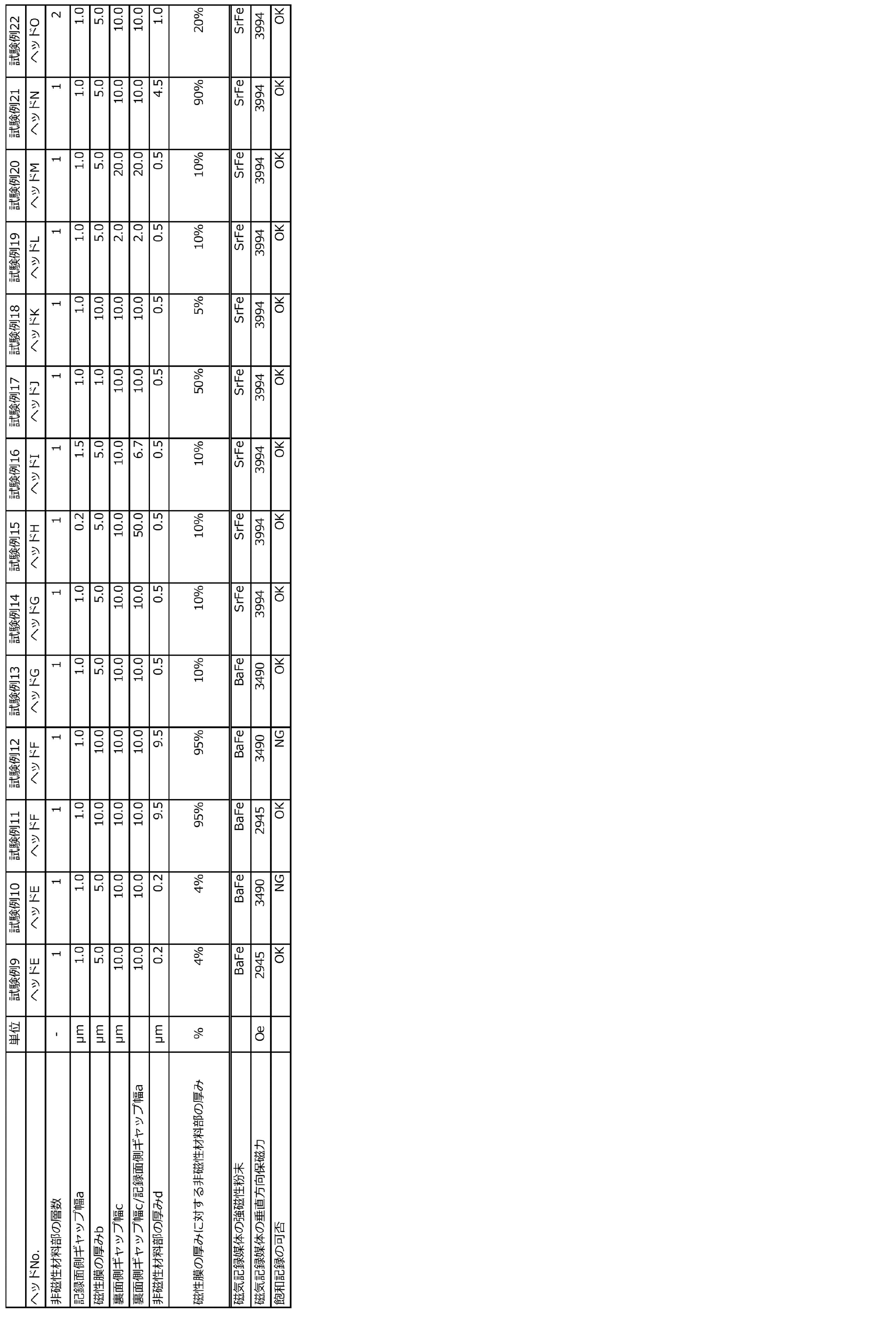
ヘッドPでは、10本のライトギャップはすべて、FIB加工によって磁性膜に貫通穴として開口部が形成されたライトギャップである。上記で作製した断面試料をSEM観察したところ、各ライトギャップのFIB加工により形成された貫通穴の断面形状は、記録面側から裏面側に向かって開口幅が狭くなる逆テーパー形状であった。
ヘッドA~Oにおいて、10本のライトギャップは、ライトギャップの記録面側のギャップ端部にFIB加工により形成された開口部を有する。この開口部は、裏面側まで貫通している貫通穴である。上記で作製した断面試料をSEM観察したところ、各ライトギャップのFIB加工により形成された貫通穴の断面形状は、記録面側から裏面側に向かって開口幅が狭くなる逆テーパー形状であった。ただし、非磁性材料部が設けられているため、10本のライトギャップでは、いずれも、記録面側ギャップ幅が裏面側ギャップ幅より狭い。かかるヘッドA~Oは、表1に示すように、ヘッドPでは飽和記録不可(比較試験例1)であった保磁力以上の保磁力を有する磁気テープに飽和記録可能であった。
また、表1に示す結果において、垂直方向保磁力がより高い磁気テープに対しても飽和記録可能であるヘッドほど、記録能力が高いということができる。
尚、ヘッドA~Pにおいて、記録面側の磁性膜表面のFIB加工によって形成された開口部近傍を光学顕微鏡で観察したところ、FIB加工の加工対象領域を指定するために走査イオン顕微鏡(SIM)で撮像を行った際のイオン照射によって変質した部分(所謂焼け跡)が確認された。
ヘッドA~Oにおいて、10本のライトギャップは、ライトギャップの記録面側のギャップ端部にFIB加工により形成された開口部を有する。この開口部は、裏面側まで貫通している貫通穴である。上記で作製した断面試料をSEM観察したところ、各ライトギャップのFIB加工により形成された貫通穴の断面形状は、記録面側から裏面側に向かって開口幅が狭くなる逆テーパー形状であった。ただし、非磁性材料部が設けられているため、10本のライトギャップでは、いずれも、記録面側ギャップ幅が裏面側ギャップ幅より狭い。かかるヘッドA~Oは、表1に示すように、ヘッドPでは飽和記録不可(比較試験例1)であった保磁力以上の保磁力を有する磁気テープに飽和記録可能であった。
また、表1に示す結果において、垂直方向保磁力がより高い磁気テープに対しても飽和記録可能であるヘッドほど、記録能力が高いということができる。
尚、ヘッドA~Pにおいて、記録面側の磁性膜表面のFIB加工によって形成された開口部近傍を光学顕微鏡で観察したところ、FIB加工の加工対象領域を指定するために走査イオン顕微鏡(SIM)で撮像を行った際のイオン照射によって変質した部分(所謂焼け跡)が確認された。
本発明の一態様は、高密度記録を行う磁気記録の技術分野において有用である。
Claims (17)
- ライトギャップを含む磁性膜を有し、
前記ライトギャップにおいて、記録面側ギャップ幅は裏面側ギャップ幅より狭く、かつ
前記ライトギャップの記録面側のギャップ端部にイオンビーム加工により形成された開口部を有する磁気記録ヘッド。 - サーボライトヘッドである、請求項1に記載の磁気記録ヘッド。
- 前記ライトギャップの記録面側ギャップ幅は0.2μm以上1.5μm以下である、請求項1または2に記載の磁気記録ヘッド。
- 前記ライトギャップの裏面側ギャップ幅は2.0μm以上20.0μm以下である、請求項1~3のいずれか1項に記載の磁気記録ヘッド。
- 前記磁性膜の厚みは1.0μm以上10.0μm以下である、請求項1~4のいずれか1項に記載の磁気記録ヘッド。
- 前記ライトギャップは裏面側のギャップ端部に非磁性材料部を含む、請求項1~5のいずれか1項に記載の磁気記録ヘッド。
- 前記磁性膜の厚みに対して前記非磁性材料部の厚みは5%以上90%以下である、請求項6に記載の磁気記録ヘッド。
- 前記非磁性材料部を構成する非磁性材料はケイ素酸化物である、請求項6または7に記載の磁気記録ヘッド。
- 前記磁性膜は窒化鉄系合金膜である、請求項1~8のいずれか1項に記載の磁気記録ヘッド。
- 前記イオンビーム加工は集束イオンビーム加工である、請求項1~9のいずれか1項に記載の磁気記録ヘッド。
- 請求項1~10のいずれか1項に記載の磁気記録ヘッドを含む磁気記録装置。
- サーボライターである、請求項11に記載の磁気記録装置。
- 請求項1~10のいずれか1項に記載の磁気記録ヘッドの製造方法であって、
基板上に非磁性材料部を形成すること、
前記基板上に前記非磁性材料部を覆うように磁性膜を形成すること、
前記磁性膜のライトギャップを形成すべき部分にイオンビーム加工によって開口部を形成すること、
を含み、かつ
前記イオンビーム加工される部分は、前記磁性膜と前記基板との間に前記非磁性材料部を有する、前記製造方法。 - 前記イオンビーム加工は集束イオンビーム加工である、請求項13に記載の磁気記録ヘッドの製造方法。
- 磁気記録媒体に請求項1~10のいずれか1項に記載の磁気記録ヘッドによってサーボパターンを形成することを含む、サーボパターンを有する磁気記録媒体の製造方法。
- 前記サーボパターンはタイミングベースサーボパターンである、請求項15に記載の磁気記録媒体の製造方法。
- 前記磁気記録媒体の垂直方向保磁力は2800Oe以上である、請求項15または16に記載の磁気記録媒体の製造方法。
Priority Applications (2)
| Application Number | Priority Date | Filing Date | Title |
|---|---|---|---|
| CN202180065537.4A CN116324986A (zh) | 2020-09-25 | 2021-09-09 | 磁记录头及其制造方法、磁记录装置和磁记录介质的制造方法 |
| US18/188,609 US12087334B2 (en) | 2020-09-25 | 2023-03-23 | Magnetic recording head and manufacturing method thereof, magnetic recording apparatus, and manufacturing method of magnetic recording medium |
Applications Claiming Priority (2)
| Application Number | Priority Date | Filing Date | Title |
|---|---|---|---|
| JP2020-160905 | 2020-09-25 | ||
| JP2020160905A JP7377182B2 (ja) | 2020-09-25 | 2020-09-25 | 磁気記録ヘッドおよびその製造方法、磁気記録装置ならびに磁気記録媒体の製造方法 |
Related Child Applications (1)
| Application Number | Title | Priority Date | Filing Date |
|---|---|---|---|
| US18/188,609 Continuation US12087334B2 (en) | 2020-09-25 | 2023-03-23 | Magnetic recording head and manufacturing method thereof, magnetic recording apparatus, and manufacturing method of magnetic recording medium |
Publications (1)
| Publication Number | Publication Date |
|---|---|
| WO2022065044A1 true WO2022065044A1 (ja) | 2022-03-31 |
Family
ID=80845245
Family Applications (1)
| Application Number | Title | Priority Date | Filing Date |
|---|---|---|---|
| PCT/JP2021/033107 Ceased WO2022065044A1 (ja) | 2020-09-25 | 2021-09-09 | 磁気記録ヘッドおよびその製造方法、磁気記録装置ならびに磁気記録媒体の製造方法 |
Country Status (4)
| Country | Link |
|---|---|
| US (1) | US12087334B2 (ja) |
| JP (1) | JP7377182B2 (ja) |
| CN (1) | CN116324986A (ja) |
| WO (1) | WO2022065044A1 (ja) |
Families Citing this family (1)
| Publication number | Priority date | Publication date | Assignee | Title |
|---|---|---|---|---|
| JP7845896B2 (ja) | 2022-03-29 | 2026-04-14 | 株式会社サトー | プリンタ、プリンタの制御方法、及びプログラム |
Citations (8)
| Publication number | Priority date | Publication date | Assignee | Title |
|---|---|---|---|---|
| JPH06333210A (ja) * | 1993-05-24 | 1994-12-02 | Mitsubishi Electric Corp | 薄膜磁気ヘッドの製法 |
| JPH09326113A (ja) * | 1996-06-06 | 1997-12-16 | Victor Co Of Japan Ltd | 磁気記録媒体及び磁気記録再生方式 |
| JP2001256614A (ja) * | 2000-03-13 | 2001-09-21 | Hitachi Ltd | 薄膜磁気ヘッド及びその製造方法 |
| JP2005222570A (ja) * | 2004-02-03 | 2005-08-18 | Canon Inc | 磁気ヘッド及びその製造方法 |
| JP2006260745A (ja) * | 2005-02-18 | 2006-09-28 | Showa Denko Kk | 垂直磁気記録媒体および磁気記録装置 |
| JP2007149155A (ja) * | 2005-11-24 | 2007-06-14 | Hitachi Ltd | 磁気記録媒体、その作製方法、及び磁気ディスク装置 |
| JP2020013630A (ja) * | 2013-03-15 | 2020-01-23 | ソニー株式会社 | 磁気記録媒体、サーボ信号記録装置及び磁気記録媒体の製造方法 |
| JP2020024776A (ja) * | 2011-06-13 | 2020-02-13 | ソニー株式会社 | 垂直異方性を有する磁気記録媒体のサーボ書き込み |
Family Cites Families (29)
| Publication number | Priority date | Publication date | Assignee | Title |
|---|---|---|---|---|
| FR2604021B1 (fr) * | 1986-09-17 | 1988-10-28 | Commissariat Energie Atomique | Procede de realisation de tetes magnetiques en couches minces et a structure planaire et tete obtenue par ce procede |
| FR2658646B1 (fr) * | 1990-02-21 | 1995-07-13 | Commissariat Energie Atomique | Procede de realisation d'une tete magnetique a deux materiaux magnetiques, et tete obtenue par ce procede. |
| JPH0440613A (ja) * | 1990-06-07 | 1992-02-12 | Mitsubishi Electric Corp | 薄膜磁気ヘッド素子 |
| JP3200060B2 (ja) * | 1990-09-12 | 2001-08-20 | ソニー株式会社 | 薄膜磁気ヘッド |
| US5689384A (en) * | 1994-06-30 | 1997-11-18 | International Business Machines Corporation | Timing based servo system for magnetic tape systems |
| FR2724480B1 (fr) * | 1994-09-13 | 1996-12-06 | Commissariat Energie Atomique | Tete magnetique a pieces polaires horizontales |
| US5572392A (en) * | 1994-11-17 | 1996-11-05 | International Business Machines Corporation | Arbitrary pattern write head assembly for writing timing-based servo patterns on magnetic storage media |
| CN1080424C (zh) * | 1995-06-16 | 2002-03-06 | 三洋电机株式会社 | 磁头及其制造方法 |
| US5793577A (en) * | 1996-11-01 | 1998-08-11 | Read-Rite Corporation | Planar geometry thin film head with shaped poles |
| US6236537B1 (en) * | 1997-10-28 | 2001-05-22 | Hewlett-Packard Co. | Wear resistant magnetic write head |
| JP3790347B2 (ja) * | 1997-11-26 | 2006-06-28 | Tdk株式会社 | 薄膜磁気ヘッドの製造方法 |
| US6269533B2 (en) | 1999-02-23 | 2001-08-07 | Advanced Research Corporation | Method of making a patterned magnetic recording head |
| JP3569462B2 (ja) * | 1999-06-02 | 2004-09-22 | 富士通株式会社 | Mrヘッドの製造方法 |
| US6879457B2 (en) * | 2002-02-13 | 2005-04-12 | International Business Machines Corporation | Timing based servo with fixed distances between transitions |
| JP4076889B2 (ja) * | 2003-03-26 | 2008-04-16 | Tdk株式会社 | 磁気記録媒体の製造方法 |
| JP2005085390A (ja) * | 2003-09-09 | 2005-03-31 | Fuji Photo Film Co Ltd | 複合型磁気ヘッド及びその製造方法 |
| JP2005166193A (ja) * | 2003-12-04 | 2005-06-23 | Fuji Photo Film Co Ltd | 複合型磁気ヘッド及びその製造方法 |
| US7800862B1 (en) * | 2004-02-18 | 2010-09-21 | Advanced Research Corporation | Magnetic recording head having secondary sub-gaps |
| US20100321824A1 (en) * | 2004-02-18 | 2010-12-23 | Dugas Matthew P | Magnetic recording head having secondary sub-gaps |
| US7199957B2 (en) * | 2004-03-30 | 2007-04-03 | Imation Corp. | Write head alignment for full amplitude time-based servo |
| US7119976B2 (en) * | 2005-01-12 | 2006-10-10 | International Business Machines Corporation | Planar servo format verifier head |
| JP2007164861A (ja) * | 2005-12-12 | 2007-06-28 | Fujitsu Ltd | 磁気ヘッド |
| US8014100B2 (en) * | 2007-05-04 | 2011-09-06 | International Business Machines Corporation | Planar servo write head |
| JP5427441B2 (ja) * | 2009-03-11 | 2014-02-26 | 昭和電工株式会社 | 磁気記録媒体の製造方法 |
| JP2011233199A (ja) * | 2010-04-27 | 2011-11-17 | Showa Denko Kk | 磁気記録媒体の製造方法、及び磁気記録再生装置 |
| US8804276B2 (en) | 2011-06-13 | 2014-08-12 | Imation Corp. | Continuous biasing and servowriting of magnetic storage media having perpendicular anisotropy |
| US8711512B2 (en) * | 2011-10-24 | 2014-04-29 | International Business Machines Corporation | Servo write assembly |
| JP6206252B2 (ja) * | 2013-03-15 | 2017-10-04 | ソニー株式会社 | 磁気記録媒体、サーボ信号記録装置及び磁気記録媒体の製造方法 |
| WO2020203785A1 (ja) * | 2019-03-29 | 2020-10-08 | ソニー株式会社 | 磁気記録媒体及びサーボ信号記録装置 |
-
2020
- 2020-09-25 JP JP2020160905A patent/JP7377182B2/ja active Active
-
2021
- 2021-09-09 WO PCT/JP2021/033107 patent/WO2022065044A1/ja not_active Ceased
- 2021-09-09 CN CN202180065537.4A patent/CN116324986A/zh active Pending
-
2023
- 2023-03-23 US US18/188,609 patent/US12087334B2/en active Active
Patent Citations (8)
| Publication number | Priority date | Publication date | Assignee | Title |
|---|---|---|---|---|
| JPH06333210A (ja) * | 1993-05-24 | 1994-12-02 | Mitsubishi Electric Corp | 薄膜磁気ヘッドの製法 |
| JPH09326113A (ja) * | 1996-06-06 | 1997-12-16 | Victor Co Of Japan Ltd | 磁気記録媒体及び磁気記録再生方式 |
| JP2001256614A (ja) * | 2000-03-13 | 2001-09-21 | Hitachi Ltd | 薄膜磁気ヘッド及びその製造方法 |
| JP2005222570A (ja) * | 2004-02-03 | 2005-08-18 | Canon Inc | 磁気ヘッド及びその製造方法 |
| JP2006260745A (ja) * | 2005-02-18 | 2006-09-28 | Showa Denko Kk | 垂直磁気記録媒体および磁気記録装置 |
| JP2007149155A (ja) * | 2005-11-24 | 2007-06-14 | Hitachi Ltd | 磁気記録媒体、その作製方法、及び磁気ディスク装置 |
| JP2020024776A (ja) * | 2011-06-13 | 2020-02-13 | ソニー株式会社 | 垂直異方性を有する磁気記録媒体のサーボ書き込み |
| JP2020013630A (ja) * | 2013-03-15 | 2020-01-23 | ソニー株式会社 | 磁気記録媒体、サーボ信号記録装置及び磁気記録媒体の製造方法 |
Also Published As
| Publication number | Publication date |
|---|---|
| US20230230614A1 (en) | 2023-07-20 |
| CN116324986A (zh) | 2023-06-23 |
| JP7377182B2 (ja) | 2023-11-09 |
| US12087334B2 (en) | 2024-09-10 |
| JP2022053980A (ja) | 2022-04-06 |
Similar Documents
| Publication | Publication Date | Title |
|---|---|---|
| KR100272781B1 (ko) | 자기임피던스효과 소자와 이를 사용한 자기헤드,박막자기헤드, 방위센서 및 오토캔슬러 | |
| US12080322B2 (en) | Magnetic tape, magnetic tape cartridge, and magnetic tape device | |
| JP2002523849A (ja) | 薄膜シールド型磁気再生ヘッド装置 | |
| USRE38594E1 (en) | Magnetic sensing apparatus having a central core with wire therethrough | |
| KR100298818B1 (ko) | 향상된자기검출감도를갖는거대자기-저항성자기센서 | |
| JPH06338410A (ja) | 軟磁性多層膜と磁気ヘッド | |
| US12087334B2 (en) | Magnetic recording head and manufacturing method thereof, magnetic recording apparatus, and manufacturing method of magnetic recording medium | |
| EP0818038B1 (en) | Magnetic head with magnetoresistive sensor, and scanning device provided with the magnetic head | |
| WO2022211049A1 (ja) | 磁気ヘッド、サーボパターン記録装置、テープドライブ装置、磁気テープの製造方法および記録方法 | |
| KR100265984B1 (ko) | 자기 임피던스효과 소자 및 그것을 이용한 자기헤드,전자 컴파스 및 오토 캔슬러 | |
| JP2005098804A (ja) | 磁気力顕微鏡用の磁性探針およびその製造方法 | |
| JPS6141982B2 (ja) | ||
| JP2541084B2 (ja) | 薄膜磁気ヘッド | |
| JP6898963B2 (ja) | 磁気テープ装置 | |
| WO2022070967A1 (ja) | 磁気記録媒体、磁気テープカートリッジおよび磁気記録再生装置 | |
| JPS59157828A (ja) | 磁気記録媒体 | |
| Kumura et al. | The high B/sub s/sputtered amorphous MIG head with a minimized contour effect | |
| JP2003203324A (ja) | 垂直磁気記録媒体 | |
| JPH06128706A (ja) | 非晶質軟磁性材料 | |
| JPH06204020A (ja) | 非晶質軟磁性材料 | |
| JPH08279112A (ja) | 磁気ヘッド | |
| JPH1064023A (ja) | 磁気ヘッド | |
| JPS62267908A (ja) | 垂直磁気記録用磁気ヘツド | |
| JPH06243417A (ja) | 磁気ヘッドの製造方法 | |
| JP2001084520A (ja) | 磁気ヘッド、磁気ヘッド製造方法、磁気特性測定装置、及び、透磁率測定方法 |
Legal Events
| Date | Code | Title | Description |
|---|---|---|---|
| 121 | Ep: the epo has been informed by wipo that ep was designated in this application |
Ref document number: 21872175 Country of ref document: EP Kind code of ref document: A1 |
|
| NENP | Non-entry into the national phase |
Ref country code: DE |
|
| 122 | Ep: pct application non-entry in european phase |
Ref document number: 21872175 Country of ref document: EP Kind code of ref document: A1 |