WO2022065007A1 - 半導体装置、半導体モジュール、モータ駆動装置および車両 - Google Patents
半導体装置、半導体モジュール、モータ駆動装置および車両 Download PDFInfo
- Publication number
- WO2022065007A1 WO2022065007A1 PCT/JP2021/032599 JP2021032599W WO2022065007A1 WO 2022065007 A1 WO2022065007 A1 WO 2022065007A1 JP 2021032599 W JP2021032599 W JP 2021032599W WO 2022065007 A1 WO2022065007 A1 WO 2022065007A1
- Authority
- WO
- WIPO (PCT)
- Prior art keywords
- potential
- insulating
- layer
- low
- coil
- Prior art date
- Legal status (The legal status is an assumption and is not a legal conclusion. Google has not performed a legal analysis and makes no representation as to the accuracy of the status listed.)
- Ceased
Links
Images

































Classifications
-
- H—ELECTRICITY
- H10—SEMICONDUCTOR DEVICES; ELECTRIC SOLID-STATE DEVICES NOT OTHERWISE PROVIDED FOR
- H10W—GENERIC PACKAGES, INTERCONNECTIONS, CONNECTORS OR OTHER CONSTRUCTIONAL DETAILS OF DEVICES COVERED BY CLASS H10
- H10W72/00—Interconnections or connectors in packages
- H10W72/20—Bump connectors, e.g. solder bumps or copper pillars; Dummy bumps; Thermal bumps
-
- H—ELECTRICITY
- H10—SEMICONDUCTOR DEVICES; ELECTRIC SOLID-STATE DEVICES NOT OTHERWISE PROVIDED FOR
- H10W—GENERIC PACKAGES, INTERCONNECTIONS, CONNECTORS OR OTHER CONSTRUCTIONAL DETAILS OF DEVICES COVERED BY CLASS H10
- H10W20/00—Interconnections in chips, wafers or substrates
- H10W20/40—Interconnections external to wafers or substrates, e.g. back-end-of-line [BEOL] metallisations or vias connecting to gate electrodes
- H10W20/41—Interconnections external to wafers or substrates, e.g. back-end-of-line [BEOL] metallisations or vias connecting to gate electrodes characterised by their conductive parts
- H10W20/427—Power or ground buses
-
- H—ELECTRICITY
- H10—SEMICONDUCTOR DEVICES; ELECTRIC SOLID-STATE DEVICES NOT OTHERWISE PROVIDED FOR
- H10W—GENERIC PACKAGES, INTERCONNECTIONS, CONNECTORS OR OTHER CONSTRUCTIONAL DETAILS OF DEVICES COVERED BY CLASS H10
- H10W20/00—Interconnections in chips, wafers or substrates
- H10W20/40—Interconnections external to wafers or substrates, e.g. back-end-of-line [BEOL] metallisations or vias connecting to gate electrodes
- H10W20/45—Interconnections external to wafers or substrates, e.g. back-end-of-line [BEOL] metallisations or vias connecting to gate electrodes characterised by their insulating parts
- H10W20/47—Interconnections external to wafers or substrates, e.g. back-end-of-line [BEOL] metallisations or vias connecting to gate electrodes characterised by their insulating parts comprising two or more dielectric layers having different properties, e.g. different dielectric constants
-
- H—ELECTRICITY
- H10—SEMICONDUCTOR DEVICES; ELECTRIC SOLID-STATE DEVICES NOT OTHERWISE PROVIDED FOR
- H10W—GENERIC PACKAGES, INTERCONNECTIONS, CONNECTORS OR OTHER CONSTRUCTIONAL DETAILS OF DEVICES COVERED BY CLASS H10
- H10W20/00—Interconnections in chips, wafers or substrates
- H10W20/40—Interconnections external to wafers or substrates, e.g. back-end-of-line [BEOL] metallisations or vias connecting to gate electrodes
- H10W20/497—Inductive arrangements or effects of, or between, wiring layers
-
- H—ELECTRICITY
- H10—SEMICONDUCTOR DEVICES; ELECTRIC SOLID-STATE DEVICES NOT OTHERWISE PROVIDED FOR
- H10W—GENERIC PACKAGES, INTERCONNECTIONS, CONNECTORS OR OTHER CONSTRUCTIONAL DETAILS OF DEVICES COVERED BY CLASS H10
- H10W72/00—Interconnections or connectors in packages
- H10W72/90—Bond pads, in general
-
- H—ELECTRICITY
- H10—SEMICONDUCTOR DEVICES; ELECTRIC SOLID-STATE DEVICES NOT OTHERWISE PROVIDED FOR
- H10W—GENERIC PACKAGES, INTERCONNECTIONS, CONNECTORS OR OTHER CONSTRUCTIONAL DETAILS OF DEVICES COVERED BY CLASS H10
- H10W90/00—Package configurations
-
- H—ELECTRICITY
- H10—SEMICONDUCTOR DEVICES; ELECTRIC SOLID-STATE DEVICES NOT OTHERWISE PROVIDED FOR
- H10W—GENERIC PACKAGES, INTERCONNECTIONS, CONNECTORS OR OTHER CONSTRUCTIONAL DETAILS OF DEVICES COVERED BY CLASS H10
- H10W90/00—Package configurations
- H10W90/811—Multiple chips on leadframes
-
- H—ELECTRICITY
- H02—GENERATION; CONVERSION OR DISTRIBUTION OF ELECTRIC POWER
- H02M—APPARATUS FOR CONVERSION BETWEEN AC AND AC, BETWEEN AC AND DC, OR BETWEEN DC AND DC, AND FOR USE WITH MAINS OR SIMILAR POWER SUPPLY SYSTEMS; CONVERSION OF DC OR AC INPUT POWER INTO SURGE OUTPUT POWER; CONTROL OR REGULATION THEREOF
- H02M1/00—Details of apparatus for conversion
- H02M1/0003—Details of control, feedback or regulation circuits
- H02M1/0006—Arrangements for supplying an adequate voltage to the control circuit of converters
-
- H—ELECTRICITY
- H02—GENERATION; CONVERSION OR DISTRIBUTION OF ELECTRIC POWER
- H02M—APPARATUS FOR CONVERSION BETWEEN AC AND AC, BETWEEN AC AND DC, OR BETWEEN DC AND DC, AND FOR USE WITH MAINS OR SIMILAR POWER SUPPLY SYSTEMS; CONVERSION OF DC OR AC INPUT POWER INTO SURGE OUTPUT POWER; CONTROL OR REGULATION THEREOF
- H02M1/00—Details of apparatus for conversion
- H02M1/08—Circuits specially adapted for the generation of control voltages for semiconductor devices incorporated in static converters
-
- H—ELECTRICITY
- H02—GENERATION; CONVERSION OR DISTRIBUTION OF ELECTRIC POWER
- H02M—APPARATUS FOR CONVERSION BETWEEN AC AND AC, BETWEEN AC AND DC, OR BETWEEN DC AND DC, AND FOR USE WITH MAINS OR SIMILAR POWER SUPPLY SYSTEMS; CONVERSION OF DC OR AC INPUT POWER INTO SURGE OUTPUT POWER; CONTROL OR REGULATION THEREOF
- H02M7/00—Conversion of AC power input into DC power output; Conversion of DC power input into AC power output
- H02M7/003—Constructional details, e.g. physical layout, assembly, wiring or busbar connections
-
- H—ELECTRICITY
- H02—GENERATION; CONVERSION OR DISTRIBUTION OF ELECTRIC POWER
- H02P—CONTROL OR REGULATION OF ELECTRIC MOTORS, ELECTRIC GENERATORS OR DYNAMO-ELECTRIC CONVERTERS; CONTROLLING TRANSFORMERS, REACTORS OR CHOKE COILS
- H02P23/00—Arrangements or methods for the control of AC motors characterised by a control method other than vector control
-
- H—ELECTRICITY
- H10—SEMICONDUCTOR DEVICES; ELECTRIC SOLID-STATE DEVICES NOT OTHERWISE PROVIDED FOR
- H10W—GENERIC PACKAGES, INTERCONNECTIONS, CONNECTORS OR OTHER CONSTRUCTIONAL DETAILS OF DEVICES COVERED BY CLASS H10
- H10W70/00—Package substrates; Interposers; Redistribution layers [RDL]
- H10W70/40—Leadframes
- H10W70/421—Shapes or dispositions
-
- H—ELECTRICITY
- H10—SEMICONDUCTOR DEVICES; ELECTRIC SOLID-STATE DEVICES NOT OTHERWISE PROVIDED FOR
- H10W—GENERIC PACKAGES, INTERCONNECTIONS, CONNECTORS OR OTHER CONSTRUCTIONAL DETAILS OF DEVICES COVERED BY CLASS H10
- H10W72/00—Interconnections or connectors in packages
- H10W72/01—Manufacture or treatment
- H10W72/019—Manufacture or treatment of bond pads
-
- H—ELECTRICITY
- H10—SEMICONDUCTOR DEVICES; ELECTRIC SOLID-STATE DEVICES NOT OTHERWISE PROVIDED FOR
- H10W—GENERIC PACKAGES, INTERCONNECTIONS, CONNECTORS OR OTHER CONSTRUCTIONAL DETAILS OF DEVICES COVERED BY CLASS H10
- H10W72/00—Interconnections or connectors in packages
- H10W72/01—Manufacture or treatment
- H10W72/019—Manufacture or treatment of bond pads
- H10W72/01931—Manufacture or treatment of bond pads using blanket deposition
- H10W72/01933—Manufacture or treatment of bond pads using blanket deposition in liquid form, e.g. spin coating, spray coating or immersion coating
- H10W72/01935—Manufacture or treatment of bond pads using blanket deposition in liquid form, e.g. spin coating, spray coating or immersion coating by plating, e.g. electroless plating or electroplating
-
- H—ELECTRICITY
- H10—SEMICONDUCTOR DEVICES; ELECTRIC SOLID-STATE DEVICES NOT OTHERWISE PROVIDED FOR
- H10W—GENERIC PACKAGES, INTERCONNECTIONS, CONNECTORS OR OTHER CONSTRUCTIONAL DETAILS OF DEVICES COVERED BY CLASS H10
- H10W72/00—Interconnections or connectors in packages
- H10W72/01—Manufacture or treatment
- H10W72/019—Manufacture or treatment of bond pads
- H10W72/01931—Manufacture or treatment of bond pads using blanket deposition
- H10W72/01938—Manufacture or treatment of bond pads using blanket deposition in gaseous form, e.g. by CVD or PVD
-
- H—ELECTRICITY
- H10—SEMICONDUCTOR DEVICES; ELECTRIC SOLID-STATE DEVICES NOT OTHERWISE PROVIDED FOR
- H10W—GENERIC PACKAGES, INTERCONNECTIONS, CONNECTORS OR OTHER CONSTRUCTIONAL DETAILS OF DEVICES COVERED BY CLASS H10
- H10W72/00—Interconnections or connectors in packages
- H10W72/071—Connecting or disconnecting
- H10W72/075—Connecting or disconnecting of bond wires
- H10W72/07551—Connecting or disconnecting of bond wires characterised by changes in properties of the bond wires during the connecting
- H10W72/07554—Connecting or disconnecting of bond wires characterised by changes in properties of the bond wires during the connecting changes in dispositions
-
- H—ELECTRICITY
- H10—SEMICONDUCTOR DEVICES; ELECTRIC SOLID-STATE DEVICES NOT OTHERWISE PROVIDED FOR
- H10W—GENERIC PACKAGES, INTERCONNECTIONS, CONNECTORS OR OTHER CONSTRUCTIONAL DETAILS OF DEVICES COVERED BY CLASS H10
- H10W72/00—Interconnections or connectors in packages
- H10W72/50—Bond wires
- H10W72/531—Shapes of wire connectors
- H10W72/536—Shapes of wire connectors the connected ends being ball-shaped
-
- H—ELECTRICITY
- H10—SEMICONDUCTOR DEVICES; ELECTRIC SOLID-STATE DEVICES NOT OTHERWISE PROVIDED FOR
- H10W—GENERIC PACKAGES, INTERCONNECTIONS, CONNECTORS OR OTHER CONSTRUCTIONAL DETAILS OF DEVICES COVERED BY CLASS H10
- H10W72/00—Interconnections or connectors in packages
- H10W72/50—Bond wires
- H10W72/541—Dispositions of bond wires
- H10W72/5445—Dispositions of bond wires being orthogonal to a side surface of the chip, e.g. parallel arrangements
-
- H—ELECTRICITY
- H10—SEMICONDUCTOR DEVICES; ELECTRIC SOLID-STATE DEVICES NOT OTHERWISE PROVIDED FOR
- H10W—GENERIC PACKAGES, INTERCONNECTIONS, CONNECTORS OR OTHER CONSTRUCTIONAL DETAILS OF DEVICES COVERED BY CLASS H10
- H10W72/00—Interconnections or connectors in packages
- H10W72/50—Bond wires
- H10W72/541—Dispositions of bond wires
- H10W72/5449—Dispositions of bond wires not being orthogonal to a side surface of the chip, e.g. fan-out arrangements
-
- H—ELECTRICITY
- H10—SEMICONDUCTOR DEVICES; ELECTRIC SOLID-STATE DEVICES NOT OTHERWISE PROVIDED FOR
- H10W—GENERIC PACKAGES, INTERCONNECTIONS, CONNECTORS OR OTHER CONSTRUCTIONAL DETAILS OF DEVICES COVERED BY CLASS H10
- H10W72/00—Interconnections or connectors in packages
- H10W72/50—Bond wires
- H10W72/541—Dispositions of bond wires
- H10W72/547—Dispositions of multiple bond wires
-
- H—ELECTRICITY
- H10—SEMICONDUCTOR DEVICES; ELECTRIC SOLID-STATE DEVICES NOT OTHERWISE PROVIDED FOR
- H10W—GENERIC PACKAGES, INTERCONNECTIONS, CONNECTORS OR OTHER CONSTRUCTIONAL DETAILS OF DEVICES COVERED BY CLASS H10
- H10W72/00—Interconnections or connectors in packages
- H10W72/50—Bond wires
- H10W72/541—Dispositions of bond wires
- H10W72/547—Dispositions of multiple bond wires
- H10W72/5473—Dispositions of multiple bond wires multiple bond wires connected to a common bond pad
-
- H—ELECTRICITY
- H10—SEMICONDUCTOR DEVICES; ELECTRIC SOLID-STATE DEVICES NOT OTHERWISE PROVIDED FOR
- H10W—GENERIC PACKAGES, INTERCONNECTIONS, CONNECTORS OR OTHER CONSTRUCTIONAL DETAILS OF DEVICES COVERED BY CLASS H10
- H10W72/00—Interconnections or connectors in packages
- H10W72/50—Bond wires
- H10W72/59—Bond pads specially adapted therefor
-
- H—ELECTRICITY
- H10—SEMICONDUCTOR DEVICES; ELECTRIC SOLID-STATE DEVICES NOT OTHERWISE PROVIDED FOR
- H10W—GENERIC PACKAGES, INTERCONNECTIONS, CONNECTORS OR OTHER CONSTRUCTIONAL DETAILS OF DEVICES COVERED BY CLASS H10
- H10W72/00—Interconnections or connectors in packages
- H10W72/851—Dispositions of multiple connectors or interconnections
- H10W72/874—On different surfaces
- H10W72/884—Die-attach connectors and bond wires
-
- H—ELECTRICITY
- H10—SEMICONDUCTOR DEVICES; ELECTRIC SOLID-STATE DEVICES NOT OTHERWISE PROVIDED FOR
- H10W—GENERIC PACKAGES, INTERCONNECTIONS, CONNECTORS OR OTHER CONSTRUCTIONAL DETAILS OF DEVICES COVERED BY CLASS H10
- H10W72/00—Interconnections or connectors in packages
- H10W72/90—Bond pads, in general
- H10W72/921—Structures or relative sizes of bond pads
- H10W72/923—Bond pads having multiple stacked layers
-
- H—ELECTRICITY
- H10—SEMICONDUCTOR DEVICES; ELECTRIC SOLID-STATE DEVICES NOT OTHERWISE PROVIDED FOR
- H10W—GENERIC PACKAGES, INTERCONNECTIONS, CONNECTORS OR OTHER CONSTRUCTIONAL DETAILS OF DEVICES COVERED BY CLASS H10
- H10W72/00—Interconnections or connectors in packages
- H10W72/90—Bond pads, in general
- H10W72/931—Shapes of bond pads
- H10W72/932—Plan-view shape, i.e. in top view
-
- H—ELECTRICITY
- H10—SEMICONDUCTOR DEVICES; ELECTRIC SOLID-STATE DEVICES NOT OTHERWISE PROVIDED FOR
- H10W—GENERIC PACKAGES, INTERCONNECTIONS, CONNECTORS OR OTHER CONSTRUCTIONAL DETAILS OF DEVICES COVERED BY CLASS H10
- H10W72/00—Interconnections or connectors in packages
- H10W72/90—Bond pads, in general
- H10W72/931—Shapes of bond pads
- H10W72/934—Cross-sectional shape, i.e. in side view
-
- H—ELECTRICITY
- H10—SEMICONDUCTOR DEVICES; ELECTRIC SOLID-STATE DEVICES NOT OTHERWISE PROVIDED FOR
- H10W—GENERIC PACKAGES, INTERCONNECTIONS, CONNECTORS OR OTHER CONSTRUCTIONAL DETAILS OF DEVICES COVERED BY CLASS H10
- H10W72/00—Interconnections or connectors in packages
- H10W72/90—Bond pads, in general
- H10W72/941—Dispositions of bond pads
- H10W72/9415—Dispositions of bond pads relative to the surface, e.g. recessed, protruding
-
- H—ELECTRICITY
- H10—SEMICONDUCTOR DEVICES; ELECTRIC SOLID-STATE DEVICES NOT OTHERWISE PROVIDED FOR
- H10W—GENERIC PACKAGES, INTERCONNECTIONS, CONNECTORS OR OTHER CONSTRUCTIONAL DETAILS OF DEVICES COVERED BY CLASS H10
- H10W72/00—Interconnections or connectors in packages
- H10W72/90—Bond pads, in general
- H10W72/941—Dispositions of bond pads
- H10W72/944—Dispositions of multiple bond pads
- H10W72/9445—Top-view layouts, e.g. mirror arrays
-
- H—ELECTRICITY
- H10—SEMICONDUCTOR DEVICES; ELECTRIC SOLID-STATE DEVICES NOT OTHERWISE PROVIDED FOR
- H10W—GENERIC PACKAGES, INTERCONNECTIONS, CONNECTORS OR OTHER CONSTRUCTIONAL DETAILS OF DEVICES COVERED BY CLASS H10
- H10W72/00—Interconnections or connectors in packages
- H10W72/90—Bond pads, in general
- H10W72/951—Materials of bond pads
- H10W72/952—Materials of bond pads comprising metals or metalloids, e.g. PbSn, Ag or Cu
-
- H—ELECTRICITY
- H10—SEMICONDUCTOR DEVICES; ELECTRIC SOLID-STATE DEVICES NOT OTHERWISE PROVIDED FOR
- H10W—GENERIC PACKAGES, INTERCONNECTIONS, CONNECTORS OR OTHER CONSTRUCTIONAL DETAILS OF DEVICES COVERED BY CLASS H10
- H10W74/00—Encapsulations, e.g. protective coatings
-
- H—ELECTRICITY
- H10—SEMICONDUCTOR DEVICES; ELECTRIC SOLID-STATE DEVICES NOT OTHERWISE PROVIDED FOR
- H10W—GENERIC PACKAGES, INTERCONNECTIONS, CONNECTORS OR OTHER CONSTRUCTIONAL DETAILS OF DEVICES COVERED BY CLASS H10
- H10W90/00—Package configurations
- H10W90/701—Package configurations characterised by the relative positions of pads or connectors relative to package parts
- H10W90/751—Package configurations characterised by the relative positions of pads or connectors relative to package parts of bond wires
- H10W90/753—Package configurations characterised by the relative positions of pads or connectors relative to package parts of bond wires between laterally-adjacent chips
-
- H—ELECTRICITY
- H10—SEMICONDUCTOR DEVICES; ELECTRIC SOLID-STATE DEVICES NOT OTHERWISE PROVIDED FOR
- H10W—GENERIC PACKAGES, INTERCONNECTIONS, CONNECTORS OR OTHER CONSTRUCTIONAL DETAILS OF DEVICES COVERED BY CLASS H10
- H10W90/00—Package configurations
- H10W90/701—Package configurations characterised by the relative positions of pads or connectors relative to package parts
- H10W90/751—Package configurations characterised by the relative positions of pads or connectors relative to package parts of bond wires
- H10W90/756—Package configurations characterised by the relative positions of pads or connectors relative to package parts of bond wires between a chip and a stacked lead frame, conducting package substrate or heat sink
Definitions
- the present disclosure relates to a semiconductor device, a semiconductor module including a semiconductor device, a motor drive device including a semiconductor module, and a vehicle including a motor drive device.
- Patent Document 1 has a power supply, a constant current source having an output terminal powered by a power supply and connected to an anode of a temperature sensitive diode, and a non-inverting input terminal and an inverting input terminal, which are used as non-inverting input terminals. Is connected to the PWM comparator to which the voltage of the anode of the temperature sensitive diode is applied and the carrier signal (triangular wave signal) output by the carrier generation circuit is applied to the inverting input terminal, and to the output terminal of the PWM comparator. It discloses an integrated circuit comprising a photocoupler which is an insulating means for transmitting a signal from one side to the other while insulating the voltage system and the low voltage system.
- the semiconductor device includes a semiconductor layer having a main surface, a first conductive layer formed on the main surface of the semiconductor layer, and the semiconductor layer so as to cover the first conductive layer.
- a first insulating portion formed on the main surface of the above and including at least three or more first insulating layers, and formed on the first insulating portion and having a dielectric constant different from that of the first insulating layer.
- a second insulating portion including a second insulating layer not included in the first insulating portion, and the first conductive portion formed on the second insulating portion via the first insulating portion and the second insulating portion. It includes a second conductive layer facing the layer and connected to a potential different from that of the first conductive layer.
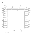
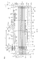
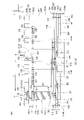
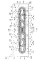
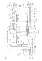
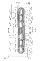
- FIG. 1 is a plan view showing a semiconductor module according to an embodiment of the present disclosure.
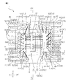
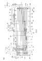
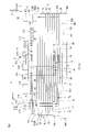
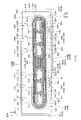
- FIG. 2 is a plan view showing the semiconductor module of FIG. 1 (sealing resin is omitted).
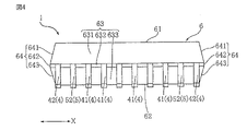
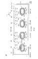
- FIG. 3 is a left side view showing the semiconductor module of FIG.
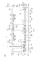
- FIG. 4 is a right side view showing the semiconductor module of FIG.
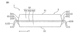
- FIG. 5 is a front view showing the semiconductor module of FIG.
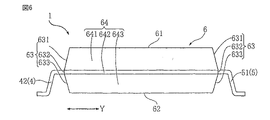
- FIG. 6 is a rear view showing the semiconductor module of FIG.
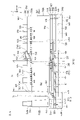
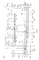
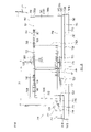
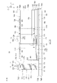
- FIG. 7 is a diagram showing a cross section of FIG. 2 VII-VII.
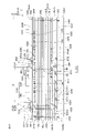
- FIG. 8 is a diagram showing a cross section of FIG. 2 VIII-VIII.
- FIG. 9 is a plan view showing a lead frame of the semiconductor module of FIG. FIG.
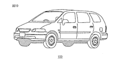
- FIG. 10 is a schematic diagram of a vehicle according to an embodiment of the present disclosure.
- FIG. 11 is a block diagram showing a configuration example of a motor drive device according to an embodiment of the present disclosure.
- FIG. 12 is a detailed view of a transmission / reception circuit portion via a transformer.
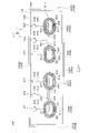
- FIG. 13 is a schematic diagram showing an example of the terminal arrangement of the semiconductor module and the chip arrangement in the sealing resin.
- FIG. 14 is an example of an explanatory table for the external terminals of the semiconductor module.
- FIG. 15 is an example of an electrical characteristic table of the semiconductor module 1.
- FIG. 16 is a circuit block diagram showing a first embodiment of a signal transmission device.
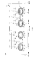
- FIG. 17 is a schematic plan view of the semiconductor device according to the embodiment of the present disclosure.
- FIG. 18 is a plan view showing a layer in which a low potential coil is formed in the semiconductor device of FIG.
- FIG. 19 is a plan view showing a layer in which a high potential coil is formed in the semiconductor device of FIG.
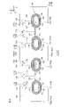
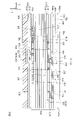
- FIG. 20 is a schematic cross-sectional view of the semiconductor device of FIG.
- FIG. 21 is an enlarged view of a main part of the semiconductor device of FIG.
- FIG. 22 is an enlarged view of the region A of FIG.
- FIG. 23 is an enlarged view of the region B of FIG.
- FIG. 24 is an enlarged view of the region C of FIG.
- FIG. 25A is a diagram showing a part of the manufacturing process of the semiconductor device of FIG.
- FIG. 25B is a diagram showing a part of the manufacturing process of the semiconductor device of FIG. FIG.
- FIG. 26A is a diagram showing the next step of FIG. 25A.
- FIG. 26B is a diagram showing the next step of FIG. 25B.
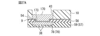
- 27A is a diagram showing the next step of FIG. 26A.
- 27B is a diagram showing the next step of FIG. 26B.
- FIG. 28A is a diagram showing the next step of FIG. 27A.
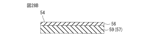
- FIG. 28B is a diagram showing the next step of FIG. 27B.
- FIG. 29A is a diagram showing the next step of FIG. 28A.
- FIG. 29B is a diagram showing the next step of FIG. 28B.
- FIG. 30A is a diagram showing the next step of FIG. 29A.
- FIG. 30B is a diagram showing the next step of FIG. 29B.
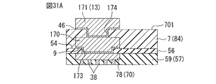
- FIG. 31A is a diagram showing the next step of FIG. 30A.
- FIG. 31B is a diagram showing the next step of FIG. 30B.
- FIG. 32A is a diagram showing the next step of FIG. 31A.
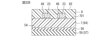
- 32B is a diagram showing the next step of FIG. 31B.
- FIG. 33 is a schematic cross-sectional view of the semiconductor device according to the embodiment of the present disclosure.
- FIG. 34 is a schematic cross-sectional view of the semiconductor device according to the embodiment of the present disclosure.
- FIG. 35 is a schematic cross-sectional view of the semiconductor device according to the embodiment of the present disclosure.
- FIG. 36 is a schematic cross-sectional view of the semiconductor device according to the embodiment of the present disclosure.
- FIG. 37 is a schematic cross-sectional view of the semiconductor device according to the embodiment of the present disclosure.
- FIG. 38 is a schematic cross-sectional view of the semiconductor device according to the embodiment of the present disclosure.
- FIG. 39 is a schematic cross-sectional view of the semiconductor device according to the embodiment of the present disclosure.
- FIG. 40 is a schematic plan view of the semiconductor device according to the embodiment of the present disclosure.
- FIG. 41 is a plan view showing a layer in which a low potential coil is formed in the semiconductor device of FIG. 40.
- FIG. 42 is a plan view showing a layer in which a high potential coil is formed in the semiconductor device of FIG. 40.
- FIG. 43 is a schematic cross-sectional view of the semiconductor device of FIG. 40.
- FIG. 44 is a schematic cross-sectional view of the semiconductor device according to the embodiment of the present disclosure.
- FIG. 44 is a schematic cross-sectional view of the semiconductor device according to the embodiment of the present disclosure.
- FIG. 45 is a schematic cross-sectional view of the semiconductor device according to the embodiment of the present disclosure.
- FIG. 46 is a schematic cross-sectional view of the semiconductor device according to the embodiment of the present disclosure.
- FIG. 47 is a schematic cross-sectional view of the semiconductor device according to the embodiment of the present disclosure.
- FIG. 48 is a schematic cross-sectional view of the semiconductor device according to the embodiment of the present disclosure.
- FIG. 49 is a schematic cross-sectional view of the semiconductor device according to the embodiment of the present disclosure.
- FIG. 50 is a schematic cross-sectional view of the semiconductor device according to the embodiment of the present disclosure.
- FIG. 51 is a schematic plan view of the semiconductor device according to the embodiment of the present disclosure.
- FIG. 52 is a plan view showing a layer in which a low potential coil is formed in the semiconductor device of FIG. 51.
- FIG. 53 is a plan view showing a layer in which a high potential coil is formed in the semiconductor device of FIG. 51.
- FIG. 54 is a schematic cross-sectional view of the semiconductor device of FIG. 51.
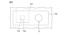
- FIG. 55 is an enlarged view of a main part of the semiconductor device of FIG. 51.
- FIG. 56 is a schematic cross-sectional view of the semiconductor device according to the embodiment of the present disclosure.
- FIG. 57 is a schematic cross-sectional view of the semiconductor device according to the embodiment of the present disclosure.
- FIG. 58 is a schematic cross-sectional view of the semiconductor device according to the embodiment of the present disclosure.
- FIG. 59 is a schematic plan view of the semiconductor device D1 according to the embodiment of the present disclosure.
- FIG. 60 is a plan view showing a layer in which the low potential coil 915 is formed in the semiconductor device D1 of FIG. 59.
- FIG. 61 is a plan view showing a layer in which the high potential coil 916 is formed in the semiconductor device D1 of FIG. 59.
- FIG. 62 is a schematic cross-sectional view of the semiconductor device D1 of FIG. 59.
- FIG. 63 is a diagram for explaining the effect of the semiconductor device of FIG. 59.
- FIG. 64 is a schematic cross-sectional view of the semiconductor device D1 according to the embodiment of the present disclosure.
- FIG. 65 is a diagram for explaining the effect of the semiconductor device of FIG. 64.
- FIG. 66 is a schematic cross-sectional view of the semiconductor device D1 according to the embodiment of the present disclosure.
- FIG. 67 is a schematic plan view of the semiconductor device E1 according to the embodiment of the present disclosure.
- FIG. 68 is a plan view showing a layer in which the low potential coil 20 is formed in the semiconductor device E1 of FIG. 67.
- FIG. 69 is a plan view showing a layer in which the high potential coil 1016 is formed in the semiconductor device E1 of FIG. 67.
- FIG. 70 is a schematic cross-sectional view of the semiconductor device E1 of FIG. 67.
- FIG. 71 is an enlarged view of a main part of the high potential coil 1016 of FIG. 70.
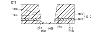
- FIG. 72 is a diagram showing steps related to the formation of the high potential coil 1016 of FIG. 71.
- FIG. 73 is a diagram showing the next step of FIG. 72.
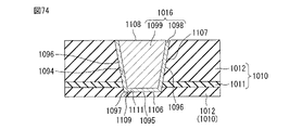
- FIG. 74 is a diagram showing the next step of FIG. 73.
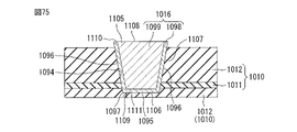
- FIG. 75 is a diagram showing the next step of FIG. 74.
- FIG. 76 is a diagram showing the next step of FIG. 75.
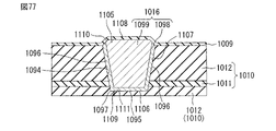
- FIG. 77 is a diagram showing the next step of FIG. 76.
- FIG. 78 is a schematic cross-sectional view of the semiconductor device E1 according to the embodiment of the present disclosure.
- FIG. 79 is a schematic cross-sectional view of the semiconductor device E1 according to the embodiment of the present disclosure.
- FIG. 80 is an enlarged view of a main part of the high potential coil 1016 of FIG.
- FIG. 81 is a diagram showing steps related to the formation of the high potential coil 1016 of FIG. 80.
- FIG. 82 is a diagram showing the next step of FIG. 81.
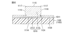
- FIG. 83 is a diagram showing the next step of FIG. 82.
- FIG. 84 is a diagram showing the next step of FIG. 83.
- FIG. 85 is a diagram showing the next step of FIG. 84.
- FIG. 86 is a schematic cross-sectional view of the semiconductor device E1 according to the embodiment of the present disclosure.
- FIG. 87 is a diagram showing a modified example of the embodiment.
- FIG. 88 is a diagram showing a modified example of the embodiment.
- FIG. 89 is a diagram showing a modified example of the embodiment.
- FIG. 87 is a diagram showing a modified example of the embodiment.
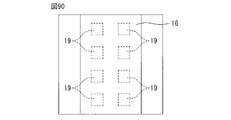
- FIG. 90 is a diagram showing a modified example of the embodiment.
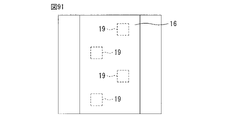
- FIG. 91 is a diagram showing a modified example of the embodiment.
- FIG. 92 is a diagram showing a modified example of the embodiment.
- FIG. 93 is a diagram showing a modified example of the embodiment.
- FIG. 94 is a diagram showing a modified example of the embodiment.
- the vertical direction of the plan view is defined as the first direction X
- the left-right direction of the plan view perpendicular to the first direction X is defined as the second direction Y.
- Both the first direction X and the second direction Y are perpendicular to the thickness direction of the semiconductor module 1.
- FIG. 1 is a plan view showing the semiconductor module 1.
- FIG. 2 is a plan view in which the sealing resin 6 described later is omitted from FIG. 1 for convenience of understanding.
- FIG. 3 is a left side view showing the semiconductor module 1.
- FIG. 4 is a right side view showing the semiconductor module 1.
- FIG. 5 is a front view showing the semiconductor module 1.
- FIG. 6 is a rear view showing the semiconductor module 1.
- FIG. 7 is a cross-sectional view taken along the line VII-VII (dashed line) of FIG.
- FIG. 8 is a cross-sectional view taken along the line VIII-VIII of FIG.
- the sealing resin 6 is illustrated by an imaginary line (dashed-dotted line).
- FIGS. 7 and 8 the sealing resin 6 is shown without omission.
- the semiconductor module 1 is surface-mounted on a circuit board of an inverter device such as an electric vehicle or a hybrid vehicle, and its package type is SOP.
- the semiconductor module 1 is not limited to SOP, but is limited to QFN (Quad For Non Lead Package), DFP (Dual Flat Package), DIP (Dual Inline Package), QFP (Quad Flat Package), SIP (Single Inline Package), or , SOJ (Small Outline J-leaded Package), or various similar package formats.
- the semiconductor module 1 includes a semiconductor element 11, an insulating element 12, a conductive support member 80, a sealing resin 6, a bonding wire 71, an interior plating layer 72, and an exterior plating layer 73.
- the semiconductor module 1 has a rectangular shape in a plan view.
- the semiconductor element 11 and the insulating element 12 are elements for making the semiconductor module 1 function.
- the semiconductor element 11 includes a control element 111 and a drive element 112.
- the control element 111 receives, for example, a circuit that converts a control signal input from the ECU into a PWM control signal, a transmission circuit for transmitting the PWM control signal to the drive element 112, and an electric signal from the drive element 112.
- the drive element 112 is for transmitting an electric signal to the control element 111, a reception circuit for receiving the PWM control signal, a circuit (gate driver) for switching a power semiconductor element such as an IGBT based on the PWM signal, and a circuit (gate driver). It has a transmission circuit. Examples of the electric signal include an output signal from a temperature sensor installed near the motor.
- the insulating element 12 is an element for transmitting the PWM control signal and other electric signals in an insulated state. Since the drive element 112 requires a higher voltage than the control element 111, a significant potential difference occurs between the control element 111 and the drive element 112, so that the insulating element 12 is required. Specifically, for example, in an inverter device of an electric vehicle or a hybrid vehicle, the power supply voltage supplied to the control element 111 is 5 V, 3.3 V, or the like with respect to the ground potential.
- a voltage of, for example, 600 V or more is transiently applied to the drive element 112 as compared with the ground potential of the control element 111.
- a half-bridge circuit in which a low-side switching element and a high-side switching element are connected in a totem pole shape is generally used for a motor driver circuit in an inverter device such as a hybrid vehicle.
- the switch that is turned on at any time is either the low-side switching element or the high-side switching element.
- the gate-source voltage operates with reference to the ground potential.
- the source of the high-side switching element and the reference potential of the isolated gate driver that drives the switching element are connected to the output node of the half-bridge circuit. Since the potential of the output node of the half-bridge circuit changes depending on whether the low-side switching element or the high-side switching element is on, the reference potential of the isolated gate driver that drives the high-side switching element changes. When the high-side switching element is on, the reference potential becomes a voltage equivalent to the voltage applied to the drain of the high-side switching element (for example, 600 V or more).
- the ground potential is separated between the driving element 112 and the control element 111 in order to ensure insulation, so that the driving element 112 has Is transiently applied with a voltage of 600 V or more as compared with the ground potential of the control element 111. Therefore, particularly in the insulated gate driver that drives the switching element on the high side side, a voltage of 600 V or more is transiently applied to the drive element 112 as compared with the ground potential of the control element 111.
- the ground potential of the drive element 112 may be the same as that of the above-mentioned external element (power transistor).
- the insulating element 12 is an inductor-coupled insulating element.
- the inductor-coupled insulating element transmits an electric signal in an insulated state by inductively coupling two inductors (coils).
- the insulating element 12 has a substrate made of Si.
- An inductor made of Cu is formed on the substrate.
- the inductor includes a transmit side inductor and a receive side inductor, and these inductors are laminated with each other in the thickness direction of the insulating element 12.
- a dielectric layer made of SiO 2 or the like is interposed between the transmitting side inductor and the receiving side inductor. The dielectric layer electrically insulates the transmitting side inductor and the receiving side inductor.
- the specific structure of the insulating element 12 will be described later.
- the insulating element 12 is located between the control element 111 and the driving element 112.
- the plan-view shapes of the control element 111, the drive element 112, and the insulating element 12 are all long rectangles having the first direction X as the long side.
- the control element 111 and the insulating element 12 are mounted on the first die pad 21 of the die pad 2, which will be described later.
- the drive element 112 is mounted on the second die pad 22 of the die pad 2 described later.
- a plurality of pads 111a are formed on the upper surface of the control element 111 (the upper surface of the control element 111 shown in FIG. 7).
- the upper surface of the drive element 112 (the upper surface of the drive element 112 shown in FIG. 7) has a plurality of pads 112a
- the upper surface of the insulating element 12 (the upper surface of the insulating element 12 shown in FIG. 7) has a plurality of pads 12a. , Each is formed.
- the conductive support member 80 is a member that mounts the semiconductor element 11 and the insulating element 12 in the semiconductor module 1 and constitutes a conductive path between the semiconductor element 11 and the insulating element 12 and the circuit board of the inverter device.
- the conductive support member 80 is made of, for example, an alloy containing Cu.
- the conductive support member 80 is formed from a lead frame 81, which will be described later.
- the conductive support member 80 includes a die pad 2, a plurality of first terminals 3, a plurality of second terminals 4, and a support terminal 5.
- the die pad 2 is a member on which the semiconductor element 11 and the insulating element 12 are mounted.
- the die pad 2 includes a first die pad 21 and a second die pad 22.
- the first die pad 21 and the second die pad 22 are arranged apart from each other.
- the area of the first die pad 21 is larger than the area of the second die pad 22.
- the plan-viewing shapes of the first die pad 21 and the second die pad 22 are both long rectangles having the first direction X as the long side.
- the first die pad 21 and the second die pad 22 are both flat.
- the first die pad 21 has a first die pad upper surface 211 and a first die pad lower surface 212.
- the upper surface 211 of the first die pad and the lower surface 212 of the first die pad face each other on opposite sides.
- the interior plating layer 72 is formed on the upper surface 211 of the first die pad.
- the control element 111 and the insulating element 12 are mounted on the interior plating layer 72 formed on the upper surface 211 of the first die pad by die bonding via a bonding layer (not shown). Further, the lower surface 212 of the first die pad is in contact with the sealing resin 6 over the entire surface.
- the second die pad 22 has a second die pad upper surface 221 and a second die pad lower surface 222.
- the upper surface 221 of the second die pad and the lower surface 222 of the second die pad face each other on opposite sides.
- the interior plating layer 72 is formed on the upper surface 221 of the second die pad.
- a driving element 112 is mounted on the interior plating layer 72 formed on the upper surface 221 of the second die pad by die bonding via a bonding layer (not shown). Further, the lower surface 222 of the second die pad is in contact with the sealing resin 6 over the entire surface.
- the sealing resin 6 is interposed between the first die pad 21 and the second die pad 22 in the second direction Y.
- the sealing resin 6 is made of, for example, a black epoxy resin having electrical insulating properties. Therefore, the first die pad 21 and the second die pad 22 are electrically insulated by the insulating element 12 and the sealing resin 6.
- the plurality of first terminals 3 are members that form a conductive path between the semiconductor module 1 and the circuit board by being joined to the circuit board of the inverter device. As shown in FIGS. 1 and 3, the plurality of first terminals 3 are arranged along the first direction X. Further, the plurality of first terminals 3 are exposed so as to extend in the second direction Y from one of the resin first side surfaces 63 of the sealing resin 6 described later.
- the plurality of first terminals 3 include a plurality of first intermediate terminals 31 and a pair of first side terminals 32.
- a plurality of first intermediate terminals 31 are arranged so as to be sandwiched between a pair of first side terminals 32.
- Each of the plurality of first intermediate terminals 31 has a lead portion 311 and a pad portion 312.
- the lead portion 311 is an elongated rectangular portion extending along the second direction Y, and as shown in FIGS. 5 and 6, the portion exposed from the first side surface 63 of the resin is bent into a gull wing shape. Has been done. Further, as shown in FIG. 7, the exterior plating layer 73 is formed so as to cover the exposed portion. The portion of the lead portion 311 on which the exterior plating layer 73 is not formed is covered with the sealing resin 6.
- the pad portion 312 is connected to the lead portion 311 and is a rectangular portion wider than the lead portion 311 in the first direction X. As shown in FIG. 7, in this embodiment, the interior plating layer 72 is formed on the upper surface of the pad portion 312. The pad portion 312 is entirely covered with the sealing resin 6. Further, the pad portion 312 is flat.
- the pair of first side terminals 32 are arranged on both sides of the plurality of first intermediate terminals 31.
- the pair of first side terminals 32 each have a lead portion 321 and a pad portion 322.
- the lead portion 321 is an elongated rectangular portion extending along the second direction Y, and as shown in FIGS. 5 and 6, the portion exposed from the first side surface 63 of the resin is bent into a gull wing shape. Has been done. Further, similarly to the lead portion 311 of the first intermediate terminal 31, the exposed portion is formed so as to be covered by the exterior plating layer 73. The portion of the lead portion 321 on which the exterior plating layer 73 is not formed is covered with the sealing resin 6.
- the pad portion 322 is connected to the lead portion 321 and is wider than the lead portion 321 in the first direction X. In this embodiment, the interior plating layer 72 is formed on the upper surface of the pad portion 322 (the surface facing the same direction as the first die pad upper surface 211 in FIG. 7), similarly to the pad portion 312 of the first intermediate terminal 31. ing. The pad portion 322 is covered with the sealing resin 6 over the entire surface. Further, the pad portion 322 is flat.
- the plurality of second terminals 4 are members that are joined to the circuit board of the inverter device to form a conductive path between the semiconductor module 1 and the circuit board. As shown in FIGS. 1 and 4, the plurality of second terminals 4 are arranged along the first direction X. Further, as shown in FIG. 2, the plurality of second terminals 4 are located on opposite sides of the plurality of first terminals 3 with the semiconductor element 11 interposed therebetween in the second direction Y. The plurality of second terminals 4 are exposed so as to extend in the second direction Y from the other resin first side surface 63 of the sealing resin 6 described later.
- the plurality of second terminals 4 include a plurality of second intermediate terminals 41 and a pair of second side terminals 42.
- a plurality of second intermediate terminals 41 are arranged so as to be sandwiched between a pair of second side terminals 42. Further, in the first direction X, the plurality of second intermediate terminals 41 are arranged so as to be sandwiched between a pair of second support terminals 52 of the support terminals 5 described later.
- Each of the plurality of second intermediate terminals 41 has a lead portion 411 and a pad portion 412.
- the lead portion 411 is an elongated rectangular portion extending along the second direction Y, and as shown in FIGS. 5 and 6, the portion exposed from the other resin first side surface 63 is bent into a gull wing shape. Has been done. Further, as shown in FIG. 7, the exterior plating layer 73 is formed so as to cover the exposed portion. The portion of the lead portion 411 on which the exterior plating layer 73 is not formed is covered with the sealing resin 6.
- the pad portion 412 is connected to the lead portion 411 and is a rectangular portion wider than the lead portion 411 in the first direction X. As shown in FIG. 7, in this embodiment, the interior plating layer 72 is formed on the upper surface of the pad portion 412 (the upper surface of the pad portion 412 shown in FIG. 7). The pad portion 412 is covered with the sealing resin 6 over the entire surface. Further, the pad portion 412 is flat. In this form, the shape of the second terminal 4 is the same as the shape of the first terminal 3.
- the pair of second side terminals 42 are arranged on both sides of the plurality of second side terminals 42.
- the pair of second side terminals 42 each have a lead portion 421 and a pad portion 422.
- the lead portion 421 is an elongated rectangular portion extending along the second direction Y, and as shown in FIGS. 5 and 6, the portion exposed from the other resin first side surface 63 is bent into a gull wing shape. Has been done. Further, similarly to the lead portion 411 of the second intermediate terminal 41, the exposed portion is formed so as to be covered by the exterior plating layer 73. The portion of the lead portion 421 on which the exterior plating layer 73 is not formed is covered with the sealing resin 6. Further, the length of the portion of the lead portion 421 covered with the sealing resin 6 is longer than the length of the portion of the lead portion 411 of the second intermediate terminal 41.
- the pad portion 422 is a portion connected to the lead portion 421 and extends in the first direction X.
- the end portion of the pad portion 422 is separated from the second die pad 22.
- the interior plating layer 72 is formed on the upper surface of the pad portion 422 (the surface facing the same direction as the upper surface 221 of the second die pad in FIG. 7), similarly to the pad portion 412 of the second intermediate terminal 41. ing.
- the pad portion 422 is entirely covered with the sealing resin 6. Further, the pad portion 422 is flat.
- the support terminal 5 is connected to the die pad 2.
- the support terminal 5 supports the die pad 2 and is joined to the circuit board of the inverter device in the same manner as the plurality of first terminals 3 and the plurality of second terminals 4, so that the semiconductor module 1 and the circuit board can be connected to each other. It is a member that constitutes a conductive path.
- the support terminal 5 includes one composed of a pair of members, and further includes a pair of first support terminals 51 and a pair of second support terminals 52. As shown in FIG. 2, the pair of first support terminals 51 are arranged apart from each other in the first direction X and are connected to both ends of the first die pad 21. Further, the pair of second support terminals 52 are arranged apart from each other in the first direction X direction and are connected to both ends of the second die pad 22.
- the pair of first support terminals 51 are arranged on both sides of the plurality of first terminals 3. Further, the pair of first support terminals 51 are exposed so as to extend in the second direction Y from the one resin first side surface 63 on which the plurality of first terminals 3 are exposed.
- the pair of first support terminals 51 each have a lead portion 511 and a pad portion 512.
- the lead portion 511 is an elongated rectangular portion extending along the second direction Y, and as shown in FIGS. 5 and 6, the portion exposed from the first side surface 63 of the resin is bent into a gull wing shape. Has been done. Further, similarly to the lead portion 311 of the first intermediate terminal 31, the exposed portion is formed so as to be covered by the exterior plating layer 73. The portion of the lead portion 511 on which the exterior plating layer 73 is not formed is covered with the sealing resin 6. Further, the length of the portion of the lead portion 511 covered with the sealing resin 6 is longer than the length of the lead portion 311 of the first intermediate terminal 31 or the lead portion 311 of the first side terminal 32.
- the pad portion 512 is a portion connected to the lead portion 511 and extends in the first direction X. As shown in FIG. 2, the end portion of the pad portion 512 is connected to the first die pad 21. As shown in FIG. 8, in this embodiment, the interior plating layer 72 is formed on the upper surface of the pad portion 512, similarly to the pad portion 312 of the first intermediate terminal 31. The pad portion 512 is covered with the sealing resin 6 over the entire surface. Further, the pad portion 512 is flat.
- a plurality of second intermediate terminals 41 are arranged inside the pair of second support terminals 52.
- the second side terminals 42 are arranged outside the pair of second support terminals 52, respectively. Therefore, the second terminals 4 are arranged on both sides of each of the pair of second support terminals 52.
- the pair of second support terminals 52 are each exposed so as to extend in the second direction Y from the other resin first side surface 63 on which the plurality of second terminals 4 are exposed.
- the pair of second support terminals 52 each have a lead portion 521, a pad portion 522, and a connecting portion 524.
- the lead portion 521 is an elongated rectangular portion extending along the second direction Y, and as shown in FIGS. 5 and 6, the portion exposed from the other resin first side surface 63 is bent into a gull wing shape. Has been done. Further, similarly to the lead portion 411 of the second intermediate terminal 41, the exposed portion is formed so as to be covered by the exterior plating layer 73. The portion of the lead portion 521 on which the exterior plating layer 73 is not formed is covered with the sealing resin 6.
- the pad portion 522 is connected to the lead portion 521 and is wider than the lead portion 521 in the first direction X. The pad portion 522 extends in the second direction Y.
- the interior plating layer 72 is formed on the upper surface of the pad portion 522 (the surface facing the same direction as the second die pad upper surface 221 in FIG. 7), similarly to the pad portion 412 of the second intermediate terminal 41. ing.
- the pad portion 522 is entirely covered with the sealing resin 6. Further, the pad portion 522 is flat.
- the connecting portion 524 is a portion connected to the pad portion 522 and extended in the first direction X. As shown in FIG. 2, the end of the connecting portion 524 is connected to the second die pad 22.
- the interior plating layer 72 is formed on the upper surface of the connecting portion 524 (the surface facing the same direction as the upper surface of the pad portion 522), similarly to the pad portion 522.
- the connecting portion 524 is covered with the sealing resin 6 over the entire surface.
- FIG. 9 is a plan view showing the lead frame 81 of the semiconductor module 1.
- the region where the sealing resin 6 is formed is shown by an imaginary line (dashed-dotted line). Further, the region where the interior plating layer 72 is formed is shown by a shaded area.
- the above-mentioned conductive support member 80 is formed from a lead frame 81.
- the die pad 2, the plurality of first terminals 3, the plurality of second terminals 4, and the support terminals 5 are all formed from the same lead frame 81.
- the lead frame 81 is made of, for example, an alloy containing Cu.
- the lead frame 81 has an outer frame 811, an island portion 812, a plurality of first leads 813, a plurality of second leads 814, a support lead 815, and a dam bar 816. Of these, the outer frame 811 and the dam bar 816 do not form the semiconductor module 1.
- the lead frame 81 will be described with reference to FIG.
- the outer frame 811 is a member formed so as to surround the island portion 812, a plurality of first leads 813, a plurality of second leads 814, a support lead 815, and a dam bar 816.
- a plurality of first leads 813, a plurality of second leads 814, and a plurality of support leads 815 are connected along the first direction X of the outer frame 811.
- the dam bar 816 is connected along the second direction Y of the outer frame 811.
- the island portion 812 is a long rectangular member having the first direction X as a long side in a plan view.
- the island portion 812 corresponds to the die pad 2.
- the island portion 812 is supported by the outer frame 811 via the support lead 815.
- the island portion 812 includes a first island portion 812a and a second island portion 812b.
- the first island portion 812a corresponds to the first die pad 21, and the second island portion 812b corresponds to the second die pad 22.
- the first island portion 812a and the second island portion 812b are arranged apart from each other.
- the plurality of first leads 813 are members arranged along the first direction X and each extending in the second direction Y.
- the plurality of first leads 813 correspond to the plurality of first terminals 3.
- One end of each first lead 813 is connected to the outer frame 811.
- the plurality of first leads 813 includes a plurality of first intermediate leads 813a and a pair of first side leads 813b.
- the first intermediate lead 813a corresponds to the first intermediate terminal 31, and the first side lead 813b corresponds to the first terminal 32.
- the plurality of second leads 814 are members arranged along the first direction X and each extending in the second direction Y. Further, the plurality of second leads 814 are located on opposite sides of the island portion 812 in the second direction Y. The plurality of second leads 814 correspond to the plurality of second terminals 4. One end of each second lead 814 is connected to the outer frame 811.
- the plurality of second leads 814 include a plurality of second intermediate leads 814a and a pair of second side leads 814b.
- the second intermediate lead 814a corresponds to the second intermediate terminal 41
- the second side lead 814b corresponds to the second side terminal 42.
- the support lead 815 is a member that extends in the second direction Y, one end of which is connected to the outer frame 811 and the other end of which is connected to the island portion 812.
- the support lead 815 corresponds to the support terminal 5.
- the support lead 815 includes a pair of first support leads 815a and a pair of second support leads 815b.
- the first support lead 815a corresponds to the first support terminal 51
- the second support lead 815b corresponds to the second support terminal 52.
- the pair of first support leads 815a are arranged apart from each other in the first direction X and are connected to both ends of the first island portion 812a.
- the pair of second support leads 815b are arranged apart from each other in the first direction X and are connected to both ends of the second island portion 812b.
- the dam bar 816 is a pair of members extending in the first direction X and having both ends connected to the outer frame 811.
- the dam bar 816 supports the plurality of first leads 813, the plurality of second leads 814, and the support leads 815 in the first direction X, respectively, and has a function of blocking the molten synthetic resin in the process of forming the sealing resin 6. Fulfill.
- One dam bar 816 is connected to a plurality of first intermediate leads 813a, a pair of first side leads 813b, and a pair of first support leads 815a.
- the other dam bar 816 is connected to a plurality of second intermediate leads 814a, a pair of second side leads 814b, and a pair of second support leads 815b.
- the sealing resin 6 is made of, for example, a black epoxy resin having electrical insulation.
- the sealing resin 6 includes a portion of each of the plurality of first terminals 3, the plurality of second terminals 4, and the support terminal 5, and the semiconductor element 11, the insulating element 12, the die pad 2, the bonding wire 71, and the interior plating layer 72. Is covering.
- the sealing resin 6 is formed by transfer molding using a mold.
- the sealing resin 6 has a resin upper surface 61, a resin lower surface 62, a pair of resin first side surfaces 63, and a pair of resin second side surfaces 64.
- the resin upper surface 61 is a surface facing upward. Further, the resin lower surface 62 is a surface facing downward. The resin upper surface 61 and the resin lower surface 62 face opposite to each other. Both the resin upper surface 61 and the resin lower surface 62 are flat.
- the pair of resin first side surfaces 63 are formed so as to be separated from each other in the second direction Y.
- the pair of resin first side surfaces 63 face each other on opposite sides.
- a plurality of first terminals 3 and a pair of first support terminals 51 are exposed from one of the resin first side surfaces 63, respectively.
- a plurality of second terminals 4 and a pair of second support terminals 52 are exposed from the other resin first side surface 63, respectively.
- each of the pair of resin first side surfaces 63 has a resin first side surface upper portion 631, a resin first side surface central portion 632, and a resin first side surface lower portion 633, respectively.
- the upper end of the resin first side surface upper portion 631 is connected to the resin upper surface surface 61, and the lower end thereof is connected to the resin first side surface central portion 632.
- the upper end of the resin first side surface upper portion 631 is inclined so that its upper end is located on the inner side of the semiconductor module 1.
- the resin first side surface central portion 632 is a portion where the upper end is connected to the resin first side surface upper portion 631 and the lower end is connected to the resin first side surface lower portion 633.
- the central portion 632 of the first side surface of the resin is perpendicular to the resin upper surface 61 and the resin lower surface 62.
- a plurality of first terminals 3 and a pair of first support terminals 51 are exposed from one of the resin first side surface central portions 632.
- a plurality of second terminals 4 and a pair of second support terminals 52 are exposed from the other resin first side surface central portion 632, respectively.
- the lower end of the resin first side surface 633 is a portion where the upper end is connected to the resin first side surface center portion 632 and the lower end is connected to the resin lower surface 62.
- the lower end of the resin first side surface lower portion 633 is inclined so that its lower end is located on the inner side of the semiconductor module 1.
- the pair of resin second side surfaces 64 are formed so as to be separated from each other in the first direction X.
- the pair of resin second side surfaces 64 face each other on opposite sides.
- the conductive support member 80 is not exposed from the pair of resin second side surfaces 64.
- the pair of resin second side surfaces 64 has a resin second side surface upper portion 641, a resin second side surface central portion 642, and a resin second side surface lower portion 643, respectively.
- the resin second side surface upper portion 641 is a portion where the upper end is connected to the resin upper surface 61 and the lower end is connected to the resin second side surface central portion 642.
- the upper end of the resin second side surface upper portion 641 is inclined so that the upper end thereof is located on the inner side of the semiconductor module 1.
- the resin second side surface central portion 642 is a portion where the upper end is connected to the resin second side surface upper portion 641 and the lower end is connected to the resin second side surface lower portion 643.
- the resin second side surface central portion 642 is perpendicular to the resin upper surface 61 and the resin lower surface 62, and is orthogonal to the resin first side surface central portion 632.
- the height of the resin second side surface central portion 642 and the height of the resin first side surface central portion 632 are substantially the same in the thickness direction of the semiconductor module 1.
- the resin second side surface lower portion 643 is a portion where the upper end is connected to the resin second side surface central portion 642 and the lower end is connected to the resin lower surface 62.
- the lower end of the resin second side surface lower portion 643 is inclined so that its lower end is located on the inner side of the semiconductor module 1.
- the plurality of bonding wires 71 are provided so that the semiconductor element 11 and the insulating element 12 perform predetermined functions together with the plurality of first terminals 3, the plurality of second terminals 4 and the support terminals 5 described above inside the semiconductor module 1. It constitutes a conductive path.
- the plurality of bonding wires 71 include a plurality of first bonding wires 711, a plurality of second bonding wires 712, a plurality of third bonding wires 713, and a plurality of fourth bonding wires 714.
- the plurality of first bonding wires 711 form a conductive path between the control element 111, the plurality of first terminals 3, and the pair of first support terminals 51.
- the plurality of first bonding wires 711 conduct the control element 111 with at least one or more first terminals 3 and first support terminals 51.
- the plurality of first bonding wires 711 are bonded to the pad 111a of the control element 111 and the pad portion 312 of the first intermediate terminal 31, the pad portion 322 of the first side terminal 32, or the pad portion 512 of the first support terminal 51, respectively. Has been done.
- the plurality of second bonding wires 712 form a conductive path between the insulating element 12 and the control element 111.
- the insulating element 12 and the control element 111 are conductive to each other by the plurality of second bonding wires 712.
- the plurality of second bonding wires 712 are bonded to the pad 12a of the insulating element 12 and the pad 111a of the control element 111, respectively.
- the plurality of second bonding wires 712 are arranged along the second direction Y.
- the plurality of third bonding wires 713 form a conductive path between the insulating element 12 and the driving element 112.
- the insulating element 12 and the driving element 112 are conductive to each other by the plurality of third bonding wires 713.
- the plurality of third bonding wires 713 are bonded to the pad 12a of the insulating element 12 and the pad 112a of the driving element 112, respectively.
- the plurality of third bonding wires 713 are arranged along the second direction Y.
- the plurality of fourth bonding wires 714 form a conductive path between the driving element 112 and the plurality of second terminals 4 and the pair of second support terminals 52.
- the drive element 112 is conductive with at least one or more second terminals 4 and second support terminals 52 by a plurality of fourth bonding wires 714.
- the plurality of fourth bonding wires 714 are bonded to the pad 112a of the drive element 112 and the pad portion 412 of the second intermediate terminal 41, the pad portion 422 of the second side terminal 42, or the pad portion 522 of the second support terminal 52, respectively. Has been done.
- FIG. 11 is a block diagram showing a configuration example of a motor drive device 101 using the semiconductor device according to the present disclosure.
- the motor drive device 101 includes a high-side switch SWH, a low-side switch SWL, a semiconductor module 1 (switch control device) which is a control means for the high-side switch SWH, and an engine control unit 102 (hereinafter, ECU [Engine Control Unit]]. 102) includes DC voltage sources E1 and E2, an npn-type bipolar transistor Q1, a pnp-type bipolar transistor Q2, capacitors C1 to C3, resistors R1 to R8, and a diode D1.
- the semiconductor module 1 is formed by sealing the control element 111 (first semiconductor chip), the driving element 112 (second semiconductor chip), and the insulating element 12 with the sealing resin 6. There is.
- the withstand voltage between input and output may be 600 V or more.
- the semiconductor module 1 may have a built-in UVLO.
- the semiconductor module 1 may have a built-in watchdog timer function.
- the semiconductor module 1 may have a built-in overcurrent protection function (automatic recovery type).
- the semiconductor module 1 may have a built-in slow-off function during the overcurrent protection operation.
- the semiconductor module 1 may have a built-in external error detection function (ERRIN).
- the semiconductor module 1 may have a built-in abnormal state output function (FLT, OCPOUT).
- the semiconductor module 1 may have a built-in active mirror clamp function.
- the semiconductor module 1 may have a built-in short circuit clamp function.
- the control element 111 is driven by being supplied with a first power supply voltage VCS1 (5 [V], 3.3 [V], etc. based on GND1) from the DC voltage source E1, and is driven by receiving a switch control signal S1 based on the input signal IN.
- the controller that generates S2 may be an integrated controller chip.
- the main functions of the control element 111 are the switch control signals S1 and S2 generation function or output function, transformer transmission abnormality monitoring function (input / output logic monitoring function of input signal IN), error state output function, UVLO function, and An external error input signal processing function can be mentioned.
- the withstand voltage of the control element 111 may be designed to an appropriate withstand voltage (for example, 7 [V] withstand voltage) in consideration of the first power supply voltage VCC1 (GND1 reference).
- the drive element 112 is driven by receiving a supply of a second power supply voltage VCS2 (10 to 30 [V] based on GND2) from the DC voltage source E2, and is a switch control signal input from the control element 111 via the insulating element 12.
- the driver chip may be an integrated driver that controls the drive of the high-side switch SWH to which a high voltage of 600 [V] or more is applied to one end.
- the main functions of the drive element 112 include an output signal OUT generation function or an output function, an overcurrent / overvoltage protection function, and a UVLO function.
- the withstand voltage of the drive element 112 may be designed to an appropriate withstand voltage (for example, 40 [V] withstand voltage) in consideration of the second power supply voltage VCS2 (GND2 standard).
- the insulating element 12 integrates a transformer that transfers the switch control signals S1 and S2, the watchdog signal S3, and the driver abnormality signal S4 while insulating the control element 111 and the drive element 112 in a direct current manner. It may be a transformer chip.
- the semiconductor module 1 is configured to independently have an insulating element 12 on which only a transformer is mounted, in addition to a control element 111 in which a controller is integrated and a drive element 112 in which a driver is integrated.
- both the control element 111 and the drive element 112 can be manufactured by a general low withstand voltage process (several [V] withstand voltage or more, several tens [V] withstand voltage or less). , It is not necessary to use a dedicated high withstand voltage process (number [kV] withstand voltage), and the manufacturing cost can be reduced.
- control element 111 and the drive element 112 can both be manufactured by an existing process with a proven track record, and there is no need to perform a new reliability test, so that the development period can be shortened and the development cost can be reduced. Can contribute to.
- the ECU 102 is a means for comprehensively performing electrical control in engine operation and motor operation, and is a microcontroller that exchanges various signals (IN, RST, FLT, OCPOUT) with the semiconductor module 1. be.
- the high-side switch SWH and the low-side switch SWL are located between the application end of the first motor drive voltage VD1 and one end of the motor coil, and between the application end of the second motor drive voltage VD2 and one end of the motor coil, respectively. It is a means for controlling the supply of the motor drive current according to each on / off control.
- an insulated gate bipolar transistor IGBT [Insulated Gate Bipolar Transistor]
- SiC A MOS [Metal Oxide Semiconductor] field effect transistor using a Silicon Carbide] semiconductor or a MOS field effect transistor using a Si semiconductor may be adopted.
- a MOS field-effect transistor using a SiC semiconductor has lower power consumption and a higher heat-resistant temperature than a MOS field-effect transistor using a Si semiconductor, and is therefore suitable for mounting in a hybrid vehicle.
- the control element 111 includes a first transmission unit 103, a second transmission unit 104, a first reception unit 105, a second reception unit 106, a logic unit 107, and a first low voltage lockout unit 108 (hereinafter, the first).
- an external error detection unit (comparator for external error detection) 109 and N-channel type MOS field effect transistors Na and Nb may be included.
- the drive element 112 includes a third receiving unit 121, a fourth receiving unit 122, a third transmitting unit 123, a fourth transmitting unit 124, a logic unit 125, a driver unit 126, and a second low voltage lockout unit.
- 127 hereinafter referred to as the second UVLO unit 127
- the overcurrent detection unit (comparator for overcurrent detection) 128, the OCP [OverCurrent Protection] timer 129 and the P-channel type MOS field effect transistors P1 and P2.
- N-channel type MOS field effect transistors N1 to N3 and SR flip-flop FF may be included.
- the insulating element 12 may include a first transformer 131, a second transformer 132, a third transformer 133, and a fourth transformer 134.
- the first transmission unit 103 is a means for transmitting the switch control signal S1 input from the logic unit 107 to the third reception unit 121 via the first transformer 131.
- the second transmission unit 104 is a means for transmitting the switch control signal S2 input from the logic unit 107 to the fourth reception unit 122 via the second transformer 132.
- the first receiving unit 105 is a means for receiving the watchdog signal S3 input from the third transmitting unit 123 via the third transformer 133 and transmitting it to the logic unit 107.
- the fourth receiving unit 122 is a means for receiving the driver abnormality signal S4 input from the fourth transmitting unit 124 via the fourth transformer 134 and transmitting it to the logic unit 107.
- the logic unit 107 exchanges various signals (IN, RST, FLT, OCPOUT) with the ECU 102, and also exchanges various signals (IN, RST, FLT, OCPOUT) with the first transmission unit 103, the second transmission unit 104, the first reception unit 105, and the second. It is a means for exchanging various signals (S1 to S4) with the driving element 112 by using the receiving unit 106.
- the logic unit 107 generates switch control signals S1 and S2 so that the output signal OUT is at a high level when the input signal IN is at a high level, and conversely, when the input signal IN is at a low level, the logic unit 107 generates the switch control signals S1 and S2.
- the switch control signals S1 and S2 are generated so that the output signal OUT is at a low level. More specifically, the logic unit 107 detects the positive edge of the input signal IN (rising edge from low level to high level) and sets a pulse to the switch control signal S1, while the negative edge of the input signal IN (high). The falling edge from the level to the low level) is detected and a pulse is generated in the switch control signal S2.
- the logic unit 107 disables the output signal OUT generation operation when the reset signal RST is at a low level, that is, switches control signals S1 and S2 so as to fix the output signal OUT at a low level. And conversely, when the reset signal RST is at a high level, the switch is controlled so that the output signal OUT generation operation is enabled, that is, the output signal OUT has a logic level corresponding to the input signal IN.
- the signals S1 and S2 are generated.
- the logic unit 107 When the reset signal RST is maintained at a low level for a predetermined time (for example, 500 [ns]), the logic unit 107 generates switch control signals S1 and S2 so as to restore the protection operation by the overcurrent detection unit 128. do.
- the logic unit 107 turns off the transistor Na and opens the first state signal FLT (pull-up state due to the resistor R1) when the semiconductor module 1 is normal, and when the semiconductor module 1 is abnormal (on the control element 111 side).
- the transistor Na is turned on and the first state signal FLT is set to a low level.
- the ECU 102 can grasp the state of the semiconductor module 1 by monitoring the first state signal FLT.
- the low voltage abnormality on the control element 111 side may be determined based on the detection result of the first UVLO unit 108, and the transformer transmission abnormality of the switch control signals S1 and S2 may be determined based on the input signal IN (switch). The determination may be made based on the comparison result between the control signals S1 and S2) and the watchdog signal S3. Further, the ERRIN signal abnormality may be determined based on the output result of the external error detection unit 109.
- the logic unit 107 turns off the transistor Nb and opens the second state signal OCPOUT (a pull-up state due to the resistor R2), and when the semiconductor module 1 is abnormal (on the drive element 112 side).
- the transistor Nb is turned on and the second state signal OCPOUT is set to the low level.
- the ECU 102 can grasp the state of the semiconductor module 1 by monitoring the second state signal OCPOUT.
- the low voltage abnormality on the drive element 112 side and the overcurrent of the motor drive current flowing through the high side switch SWH may be determined based on the driver abnormality signal S4.
- the first UVLO unit 108 is a means for monitoring whether or not the first power supply voltage VCC1 is in a low voltage state and transmitting the monitoring result to the logic unit 107.
- the external error detection unit 109 compares the voltage input to the ERRIN terminal from the connection node of the resistors R3 and R4 (the divided voltage obtained by dividing the analog voltage to be monitored by resistance) and the predetermined threshold voltage. , Is a means for transmitting the comparison result to the logic unit 107.
- the third receiving unit 121 is a means for receiving the switch control signal S1 input from the first transmitting unit 103 via the first transformer 131 and transmitting it to the set input end (S) of the SR flip-flop FF.
- the fourth receiving unit 122 is a means for receiving the switch control signal S2 input from the second transmitting unit 104 via the second transformer 132 and transmitting it to the reset input end (R) of the SR flip-flop FF.
- the third transmission unit 123 is a means for transmitting the watchdog signal S3 input from the logic unit 125 to the first reception unit 105 via the third transformer 133.
- the fourth transmission unit 124 is a means for transmitting the driver abnormality signal S4 input from the logic unit 125 to the second reception unit 106 via the fourth transformer 134.
- the SR flip-flop FF sets the output signal to a high level using the pulse edge of the switch control signal S1 input to the set input end (S) as a trigger, and sets the output signal to a high level, and the switch control signal S2 input to the reset input end (R).
- the output signal is reset to the low level triggered by the pulse edge. That is, the above output signal is the same signal as the input signal IN input from the ECU 102 to the logic unit 107.
- the above output signal is sent from the output end (Q) of the SR flip-flop FF to the logic unit 125.
- the logic unit 125 generates a drive signal for the driver unit 126 based on the output signal of the SR flip-flop FF (the same signal as the input signal IN).
- the driver unit 126 determines that a low voltage abnormality or an overcurrent has occurred based on the detection results of the second UVLO unit 127 and the overcurrent detection unit 128, the driver unit 126 notifies that fact by an abnormality detection signal. And also transmitted to the logic unit 107 by the driver abnormality signal S4. With such a configuration, even if an abnormality occurs in the drive element 112, the driver unit 126 can quickly perform a protection operation, and the logic unit 107 performs an abnormality notification operation (second state signal) to the ECU 102. OCPOUT low level transition) can be performed.
- the logic unit 125 has a function of automatically recovering from the overcurrent protection operation when a predetermined time has elapsed after the overcurrent protection operation.
- the logic unit 125 outputs the output signal of the SR flip-flop FF as a watchdog signal S3 to the third transmission unit 123 as it is.
- the configuration is such that the watchdog signal S3 is returned from the drive element 112 to the control element 111, the input signal IN input to the control element 111 and the drive element 112 with respect to the input signal IN in the logic unit 107.
- the watchdog signal S3 returned from the above it is possible to determine the presence or absence of a transformer transmission abnormality.
- the driver unit 126 is a means for controlling on / off of the transistor P1 and the transistor N1 based on the drive signal input from the logic unit 125, and outputting an output signal OUT from the connection node between the transistor P1 and the transistor N1. ..
- the output signal OUT is input to the high-side switch SWH via a drive circuit including transistors Q1 and Q2.
- the above-mentioned drive circuit is a means for adjusting the rise / fall time (slew rate) of the output signal OUT so that the output signal OUT has the drive capability of the high-side switch SWH.
- the driver unit 126 sets the transistor N2 so as to suck the electric charge (mirror current) from the gate of the high side switch SWH via the CLAMP terminal when the voltage level (GND2 reference) of the output signal OUT becomes low level. It has a function to turn it on (active mirror clamp function). With such a configuration, when the high-side switch SWH is turned off, the gate potential of the high-side switch SWH is quickly set via the transistor N2 without depending on the slew rate set in the above drive circuit. You can drop to a low level.
- the driver unit 126 turns on the transistor P2 so as to clamp the gate of the high side switch SWH to the power supply voltage VCS2 via the CLAMP terminal when the voltage level of the output signal OUT (GND2 reference) becomes high level. It has a function (short circuit clamp function). With such a configuration, when the high side switch SWH is turned on, the gate potential of the high side switch SWH does not rise to a higher potential than the power supply voltage VCS2.
- the driver unit 126 determines that it is necessary to perform a protection operation based on the abnormality detection signal input from the logic unit 125, the driver unit 126 turns off the transistors P1 and P2 and the transistors N1 and N2, while the transistor It has a function to turn on N3 (slow-off function).
- the electric charge can be extracted from the gate of the high side switch SWH through the resistor R5 more slowly than in the normal operation during the protection operation.
- the second UVLO unit 127 is a means for monitoring whether or not the second power supply voltage VCS2 is in a low voltage state and transmitting the monitoring result to the logic unit 125.
- the overcurrent detection unit 128 compares the voltage input to the OCP / DESATIN terminal from the connection node of the resistor R7 and the resistor R8 (the voltage dividing voltage obtained by dividing the anode voltage of the diode D1 into resistance) and the predetermined threshold voltage. Then, it is a means for transmitting the comparison result to the logic unit 125.
- the overcurrent detection unit 1228 when the voltage (GND2 reference) input to OCP / DESATIN reaches a predetermined threshold value (for example, 0.5 [V]), the motor drive current flowing through the high side switch SWH is excessive. It is determined that the current state is present.
- a predetermined threshold value for example, 0.5 [V]
- a configuration (voltage detection method) is adopted in which the motor drive current is detected by detecting the collector-emitter voltage of the isolated gate bipolar transistor used as the high-side switch SWH.
- the detection method of the motor drive current is not limited to this, and for example, the motor drive current flowing through the high side switch SWH (or the mirror current showing the same behavior as this).
- the OCP timer 129 is a means for counting the elapsed time after the overcurrent protection operation.
- the first transformer 131 is a DC insulating element for transmitting the switch control signal S1 from the control element 111 to the drive element 112.
- the second transformer 132 is a DC insulating element for transmitting the switch control signal S2 from the control element 111 to the drive element 112.
- the third transformer 133 is a DC insulating element for transmitting the watchdog signal S3 from the driving element 112 to the control element 111.
- the fourth transformer 134 is a DC insulating element for transmitting the driver abnormality signal S4 from the driving element 112 to the control element 111.
- the high side switch SWH is turned on / Not only off control but also various protection functions can be appropriately realized.
- FIG. 12 is a detailed view of the transmission / reception circuit portion via the transformers 131 to 134.
- the first transmission unit 103, the second transmission unit 104, the first reception unit 105, and the second reception unit 106 provided on the control element 111 side are all power supply voltages between VCS1 and GND1.
- the third receiving unit 121, the fourth receiving unit 122, the third transmitting unit 123, and the fourth transmitting unit 124 provided on the driving element 112 side are all powered by the power supply between the VCS2 and the GND2. It is driven by voltage.
- control element 111 and the drive element 112 are both manufactured by a general low withstand voltage process (several [V] withstand voltage or more, several tens [V] withstand voltage or less). Therefore, it is not necessary to use a dedicated high withstand voltage process (number [kV] withstand voltage), and the manufacturing cost can be reduced.
- FIG. 12 depicts a configuration using a comparator having a hysteresis characteristic for any of the first receiving unit 105, the second receiving unit 106, the third receiving unit 121, and the fourth receiving unit 122.
- the presence or absence of the hysteresis characteristic is arbitrary.
- UVLO1 malware prevention function at low voltage on the controller side
- the semiconductor module 1 turns off the high side switch SWH and sets the FLT terminal to the low level.
- the controller side power supply voltage voltage between VCC1 and GND1
- the semiconductor module 1 starts normal operation and opens the FLT terminal (high level).
- the semiconductor module 1 turns off the high side switch SWH and sets the OCPOUT terminal to the low level.
- the semiconductor module 1 automatically recovers after a certain period of time (t OCPRLS ) has elapsed after the overcurrent protection operation, and the OCPOUT terminal is opened (high level).
- the return time may be fixedly set inside the semiconductor module 1 or may be adjustable from the outside of the device.
- the semiconductor module 1 compares the input signal IN input from the ECU 102 to the control element 111 with the watchdog signal S3 fed back from the drive element 112 to the control element 111, and when the logics of both signals do not match. , The high side switch SWH is turned off, and the FLT terminal is set to the low level.
- the PROOUT terminal is set to a low level and the OUT terminal is set to open during the overcurrent protection operation.
- the high side switch SWH can be slowly turned off.
- the slew rate when off can be arbitrarily adjusted by appropriately selecting the resistance value of the external resistor R5.
- the CLAMP terminal is set to L.
- the high side switch SWH can be surely turned off.
- the semiconductor module 1 sets the CLAMP terminal to a high level when the applied voltage of the CLAMP terminal becomes VCS2- VSCC or higher. By such control, the gate potential of the high side switch SWH does not rise above the second power supply voltage VCS2.
- FIG. 13 is a schematic diagram showing an example of the terminal arrangement of the semiconductor module 1 and the chip arrangement in the sealing resin.
- a package has a plurality of pins arranged on two opposing sides, and as described above, the control element 111, the drive element 112, and the insulating element 12 are arranged. Are arranged perpendicular to the arrangement direction of the pins (horizontal direction of the paper surface).
- the pins 11 to 20 connected to the control element 111 and the pins 1 to 10 connected to the drive element 112 can be distributed and arranged on two opposite sides. It is possible to prevent a short circuit between the pins 11 to 20 and the pins 1 to 10 while maintaining the pin spacing to a minimum.
- Pins 11 to 20 may correspond to the first terminal 3 of FIG. 1, and pins 1 to 10 may correspond to the second terminal 4 of FIG.
- the chip arrangement when the package format is SOP is taken as an example, but when a package format other than SOP is adopted, the chip arrangement can be changed as appropriate.
- the control element 111 and the insulating element 12 are mounted on the first die pad 21 as described above, and the drive element 112 is as described above. It is mounted on the second die pad 22.
- the first die pad 21 can be used as a low voltage side island (GND1 fixed), and the second die pad 22 can be used as a high voltage side island (VEE2 fixed).
- the first die pad 21 and the second die pad 22 are both made of a non-magnetic material (for example, copper), but a magnetic material (for example, iron) may be used.
- FIG. 14 is an example of an explanation table for external terminals.
- Pin 1 (NC) is a non-connection terminal.
- Pin 2 (VEE2) is a negative power supply terminal (for example, minimum: -15V).
- the pin 3 (GND2) is a GND terminal and is connected to the emitter of the insulated gate bipolar transistor Tr1 outside the semiconductor module 1.
- Pin 4 (OCP / DESATIN) is an overcurrent detection terminal.
- Pin 5 (OUT) is an output terminal.
- Pin 6 (VCC2) is a positive power supply terminal (for example, maximum: 30V).
- Pin 7 (CLAMP) is a clamp terminal.
- Pin 8 (PROOUT) is a slow OFF output terminal.
- Pin 9 (VEE2) is a negative power supply terminal.
- Pin 10 (NC) is a non-connection terminal.
- Pin 11 is a GND terminal.
- Pin 12 is a control input terminal.
- Pin 13 is a reset input terminal.
- the pin 14 (FLT) is an output terminal of the first state signal (abnormal state detection signal on the controller chip side).
- the pin 15 is an output terminal of the second state signal (abnormal state detection signal on the driver chip side).
- Pin 16 (ERRIN) is an error detection terminal.
- Pin 17 (VCC1) is a power supply terminal (eg, 5V, 3.3V, etc.). Both pin 18 (NC) and pin 19 (NC) are non-connection terminals.
- the pin 20 (GND1) is a GND terminal.
- FIG. 16 is a circuit block diagram showing a first embodiment of the signal transmission device 200.
- the signal transmission device 200 of the present embodiment has switch control signals S1 and S2 from the primary side circuit to the secondary side circuit in a state where the ground voltage GND1 of the primary side circuit and the ground voltage GND2 of the secondary side circuit are isolated from each other.
- the unit 122 and the SR flip flop FF are included. All of these circuit blocks are the ones mentioned above in FIGS.
- the logic unit 107 and the third receiver unit are used. Ingenuity is devised in the configuration of 121 and the fourth receiving unit 122. In the following, the characteristic components will be mainly described.
- the logic unit 107 includes inverters 107-1 and 107-2, a first pulse generation unit 107-3, and a second pulse generation unit 107-4.
- the input end of the inverter 107-1 is connected to the input end of the input signal IN.
- the output end of the inverter 107-1 is connected to the input end of the inverter 107-2, while it is also connected to the input end of the second pulse generation unit 107-4.
- the output end of the inverter 107-2 is connected to the input end of the first pulse generation unit 107-3.
- the first pulse generation unit 107-3 emits N to the first transformer drive signal S1a (however, N ⁇ 2) according to the positive edge of the input signal IN input via the inverters 107-2 and 107-3. Generate a pulse.
- the first transformer drive signal S1a is output to the primary winding of the first transformer 131 via the buffer 103-1 forming the first transmission unit 103.
- the second pulse generation unit 107-4 emits N to the second transformer drive signal S2a in response to the positive edge of the inverting input signal INB (that is, the negative edge of the input signal IN) input from the inverter 107-2. Generate a pulse of N ⁇ 2).
- the second transformer drive signal S2a is output to the primary winding of the second transformer 132 via the buffer 104-1 forming the second transmission unit 104.
- the logic unit 107 continuously transmits N pulses to the first transformer drive signal S1a according to the positive edge in which the input signal IN changes from the low level to the high level. It functions as a transformer drive signal generation unit that continuously generates N pulses to the second transformer drive signal S2a according to the negative edge at which the input IN signal changes from high level to low level.
- the first transformer 131 generates a first induced signal S1b in the secondary winding in response to the first transformer drive signal S1a input to the primary winding.
- the second transformer 132 generates a second induced signal S2b in the secondary winding in response to the second transformer drive signal S2a input to the primary winding.
- the third receiving unit 121 has a first comparator 121-1 that compares the first induced signal S1b with a predetermined threshold voltage to generate the first comparison signal S1c, and the first comparison signal S1c is continuously connected with N pulses. It has a first pulse detection unit 121-2, which detects that the signal has occurred and generates a pulse in the first detection signal 1d.
- the fourth receiving unit 122 compares the second induced signal S2b with a predetermined threshold voltage to generate the second comparison signal S2c, and the second comparator 122-1 and the second comparison signal 2c are continuously connected with N pulses. It has a second pulse detection unit 122-2, which detects that the signal has occurred and generates a pulse in the second detection signal 2d.
- the SR flip-flop FF changes the output signal OUT from low level to high level according to the pulse generated in the first detection signal S1d input to the set input end (S), and inputs the output signal OUT to the reset input end (R).
- the output signal OUT is changed from high level to low level according to the pulse generated in the second detection signal S2d.
- the switch control signal S1 described above takes various signal forms such as a first transformer drive signal S1a, a first induced signal S1b, a first comparison signal S1c, and a first detection signal S1d, and is a logic unit. It is transmitted from 107 to the SR flip-flop FF.
- the switch control signal S2 described above takes various signal forms such as a second transformer drive signal S2a, a second induced signal S2b, a second comparison signal S2c, and a second detection signal S2d, and is a logic. It is transmitted from the unit 107 to the SR flip-flop FF.
- FIG. 17 is a schematic plan view of the semiconductor device A1 according to the embodiment of the present disclosure.
- FIG. 18 is a plan view showing a layer in which the low potential coil 20 is formed in the semiconductor device A1 of FIG.
- FIG. 19 is a plan view showing a layer in which the high potential coil 23 is formed in the semiconductor device A1 of FIG. FIG.
- FIG. 20 is a schematic cross-sectional view of the semiconductor device A1 of FIG.
- FIG. 21 is an enlarged view of a main part of the semiconductor device A1 of FIG.
- FIG. 22 is an enlarged view of the region A of FIG.
- FIG. 23 is an enlarged view of the region B of FIG.
- FIG. 24 is an enlarged view of the region C of FIG.
- the semiconductor device A1 includes a rectangular parallelepiped semiconductor chip 40.
- the semiconductor chip 40 includes at least one of silicon, a wide bandgap semiconductor and a compound semiconductor.
- the wide bandgap semiconductor is composed of a semiconductor that exceeds the bandgap of silicon (about 1.12 eV). Wide bandgap The bandgap of the semiconductor is preferably 2.0 eV or more.
- the wide bandgap semiconductor may be SiC (silicon carbide).
- the compound semiconductor may be a group III-V compound semiconductor.
- the compound semiconductor may contain at least one of AlN (aluminum nitride), InN (indium nitride), GaN (gallium nitride) and GaAs (gallium arsenide).
- the semiconductor chip 40 includes a semiconductor substrate made of silicon.
- the semiconductor chip 40 may be an epitaxial substrate having a laminated structure including a silicon semiconductor substrate and a silicon epitaxial layer.
- the conductive type of the semiconductor substrate may be n-type or p-type.
- the epitaxial layer may be n-type or p-type. Further, the semiconductor chip 40 may be fixed to the ground potential.
- the semiconductor chip 40 has a first main surface 401 on one side, a second main surface 402 on the other side, and chip side walls 44A to 44D connecting the first main surface 401 and the second main surface 402.
- the first main surface 401 and the second main surface 402 are formed in a rectangular shape (rectangular shape in this form) in a plan view (hereinafter, simply referred to as "planar view") viewed from their normal direction Z. ..
- the chip side walls 44A to 44D include a first chip side wall 44A, a second chip side wall 44B, a third chip side wall 44C, and a fourth chip side wall 44D.
- the first chip side wall 44A and the second chip side wall 44B form the long side of the semiconductor chip 40.
- the first chip side wall 44A and the second chip side wall 44B extend along the first direction X and face the second direction Y.
- the third chip side wall 44C and the fourth chip side wall 44D form the short side of the semiconductor chip 40.
- the third chip side wall 44C and the fourth chip side wall 44D extend in the second direction Y and face the first direction X.
- the chip side walls 44A to 44D are composed of a ground surface.
- the semiconductor device A1 includes a first insulating portion 50, a second insulating portion 7, and a protective layer 8 formed in order on the first main surface 401 of the semiconductor chip 40.
- the first insulating portion 50 has an insulating main surface 54 and insulating side walls 53A to 53D.
- the insulating main surface 54 is formed in a rectangular shape (rectangular shape in this form) that matches the first main surface 401 in a plan view.
- the insulating main surface 54 extends parallel to the first main surface 401.
- the insulating side walls 53A to 53D include a first insulating side wall 53A, a second insulating side wall 53B, a third insulating side wall 53C, and a fourth insulating side wall 53D.
- the insulating side walls 53A to 53D extend from the peripheral edge of the insulating main surface 54 toward the semiconductor chip 40 and are connected to the chip side walls 44A to 44D. Specifically, the insulating side walls 53A to 53D are formed flush with respect to the chip side walls 44A to 44D.
- the insulating side walls 53A to 53D form a flush grinding surface on the chip side walls 44A to 44D.
- the second insulating portion 7 is formed on the insulating main surface 54, and has the insulating main surface 701 and the insulating side walls 702A to 702D.
- the insulating main surface 701 is formed in a rectangular shape (rectangular shape in this form) that matches the first main surface 401 in a plan view.
- the insulating main surface 701 extends parallel to the first main surface 401.
- the insulating side walls 702A to 702D include a first insulating side wall 702A, a second insulating side wall 702B, a third insulating side wall 702C, and a fourth insulating side wall 702D.
- the insulating side walls 702A to 702D extend from the peripheral edge of the insulating main surface 701 toward the semiconductor chip 40.
- the insulating side walls 702A to 702D are formed inside the insulating side walls 53A to 53D. As a result, a step is formed between the insulating side walls 702A to 702D and the insulating side walls 53A to 53D.
- the protective layer 8 is formed on the insulating main surface 701, and has the protective main surface 82 and the protective side walls 83A to 83D.
- the protective main surface 82 is formed in a rectangular shape (rectangular shape in this form) that matches the first main surface 401 in a plan view.
- the protective main surface 82 extends parallel to the first main surface 401.
- the protective side walls 83A to 83D include a first protective side wall 83A, a second protective side wall 83B, a third protective side wall 83C, and a fourth protective side wall 83D.
- the protective side walls 83A to 83D extend from the peripheral edge of the protective main surface 82 toward the semiconductor chip 40.
- the protective side walls 83A to 83D are formed inside the insulating side walls 702A to 702D.
- a step is formed between the protective side walls 83A to 83D and the insulating side walls 702A to 702D.
- the first insulating portion 50 is composed of a multilayer insulating laminated structure including a lowermost insulating layer 55, an uppermost insulating layer 56, and a plurality of (10 layers in this form) interlayer insulating layers 57.
- the bottom insulating layer 55 is an insulating layer that directly covers the first main surface 401.
- the uppermost insulating layer 56 is an insulating layer forming the insulating main surface 54.
- the plurality of interlayer insulating layers 57 are insulating layers interposed between the lowermost insulating layer 55 and the uppermost insulating layer 56.
- the bottom insulating layer 55 in this form, has a single layer structure containing silicon oxide.
- the uppermost insulating layer 56 has a single-layer structure including silicon nitride in this form.
- the thickness of the lowermost insulating layer 55 may be 0.5 ⁇ m or more and 3 ⁇ m or less (for example, about 1 ⁇ m), and the thickness of the uppermost insulating layer 56 is 0.2 ⁇ m or more and 4 ⁇ m or less (for example, about 1 ⁇ m). May be good.
- the plurality of interlayer insulating layers 57 each have a laminated structure including a first insulating layer 58 on the lowermost insulating layer 55 side and a second insulating layer 59 on the uppermost insulating layer 56 side.
- the first insulating layer 58 is made of an inorganic insulating layer and may contain, for example, silicon nitride.
- the first insulating layer 58 is formed as an etching stopper layer for the second insulating layer 59.
- the thickness of the first insulating layer 58 may be 0.1 ⁇ m or more and 1 ⁇ m or less (for example, about 0.3 ⁇ m).
- the second insulating layer 59 is formed on the first insulating layer 58. It contains an insulating material different from that of the first insulating layer 58.
- the second insulating layer 59 is made of an inorganic insulating layer different from that of the first insulating layer 58, and may contain, for example, silicon oxide.
- the thickness of the second insulating layer 59 may be 1 ⁇ m or more and 3 ⁇ m or less (for example, about 2 ⁇ m). The thickness of the second insulating layer 59 preferably exceeds the thickness of the first insulating layer 58.
- the first insulating layer 58 may be a compressive stress film
- the second insulating layer 59 may be a tensile stress film. That is, the interlayer insulating layer 57 may have a structure in which a compressive stress film and a tensile stress film are repeatedly laminated. As a result, the first insulating portion 50 can be formed while canceling the stress at the laminated interface of the interlayer insulating layer 57. As a result, it is possible to prevent the semiconductor wafer, which is the base of the semiconductor chip 40, from being significantly warped and deformed in the manufacturing process of the semiconductor device A1.
- the compressive stress film may be, for example, a silicon oxide film
- the tensile stress film may be, for example, a silicon nitride film.
- the total thickness TA1 of the first insulating portion 50 may be 5 ⁇ m or more and 50 ⁇ m or less.
- the total thickness TA1 of the first insulating portion 50 and the number of layers of the interlayer insulating layer 57 are arbitrary, and are adjusted according to the withstand voltage (dielectric breakdown withstand) to be realized.
- the insulating materials of the lowermost insulating layer 55, the uppermost insulating layer 56, and the interlayer insulating layer 57 are arbitrary and are not limited to a specific insulating material.
- the second insulating portion 7 is made of an insulating material having a dielectric constant different from that of the first insulating layer 58 and the second insulating layer 59, and has a layer structure including, for example, an organic insulating layer 84.
- the second insulating portion 7 is composed of a single layer of the organic insulating layer 84, but may have a laminated structure of a plurality of organic insulating layers.
- the organic insulating layer 84 include a polyimide film, a phenol resin film, an epoxy resin film, and the like.
- the total thickness TA2 of the second insulating portion 7 may be 2 ⁇ m or more and 100 ⁇ m or less.
- the total thickness TA2 of the second insulating portion 7 is arbitrary, and is adjusted according to the withstand voltage (dielectric breakdown resistance) to be realized.
- the semiconductor device A1 includes the first functional device 45.
- the first functional device 45 includes one or more (plural in this form) transformers 15 (transformers). That is, the semiconductor device A1 is composed of a multi-channel device including a plurality of transformers 15.
- the plurality of transformers 15 are formed in the inner portion of the laminated structure of the first insulating portion 50 and the second insulating portion 7 at intervals from the insulating side walls 53A to 53D.
- the plurality of transformers 15 are formed at intervals in the first direction X.
- the plurality of transformers 15 are the first transformer 15A, the second transformer 15B, the third transformer 15C, and the fourth transformer 15D formed in this order from the insulating side wall 53C side to the insulating side wall 53D side in a plan view.
- the first transformer 15A, the second transformer 15B, the third transformer 15C, and the fourth transformer 15D correspond to the first transformer 131, the second transformer 132, the third transformer 133, and the fourth transformer 134 in FIG. 11, respectively. May be good.
- the plurality of transformers 15A to 15D each have a similar structure.
- the structure of the first transformer 15A will be described as an example.
- the description of the structure of the second transformer 15B, the third transformer 15C and the fourth transformer 15D the description of the structure of the first transformer 15A shall be applied mutatis mutandis and will be omitted.
- the first transformer 15A includes a low potential coil 20 and a high potential coil 23.
- the low potential coil 20 is formed in the first insulating portion 50.
- the high-potential coil 23 is formed on the second insulating portion 7 so as to face the low-potential coil 20 in the normal direction Z.
- the low-potential coil 20 is formed in a region sandwiched between the lowermost insulating layer 55 and the uppermost insulating layer 56 (that is, a plurality of interlayer insulating layers 57).
- the high potential coil 23 is formed on the insulating main surface 701 of the second insulating portion 7. That is, the high-potential coil 23 faces the semiconductor chip 40 with the low-potential coil 20 interposed therebetween.
- the location of the low-potential coil 20 and the high-potential coil 23 is arbitrary. Further, the high-potential coil 23 may face the low-potential coil 20 with at least three or more layers of the interlayer insulating layer 57 and the second insulating portion 7 interposed therebetween.
- the distance D2 between the low-potential coil 20 and the high-potential coil 23 (that is, the number of layers of the interlayer insulating layer 57 and the thickness of the second insulating portion 7) is the insulation withstand voltage between the low-potential coil 20 and the high-potential coil 23. It is adjusted appropriately according to the electric potential strength.
- the low-potential coil 20 is formed in the interlayer insulating layer 57, which is the third layer counting from the lowermost insulating layer 55 side.
- the high potential coil 23 is formed on the insulating main surface of the second insulating portion 7. Therefore, seven layers of the interlayer insulating layer 57 and the second insulating portion 7 are interposed between the low-potential coil 20 and the high-potential coil 23.
- the low-potential coil 20 is embedded in the interlayer insulating layer 57 so as to penetrate the first insulating layer 58 and the second insulating layer 59. As shown in FIG. 18, the low-potential coil 20 has a first spirally routed between the first inner end 24, the first outer end 25, and the first inner end 24 and the first outer end 25.
- the spiral portion 26 is included.
- the first spiral portion 26 is drawn in a spiral shape extending in an elliptical shape (oval shape) in a plan view.
- the portion forming the innermost peripheral edge of the first spiral portion 26 defines the elliptical first inner region 66 in a plan view.
- the number of turns of the first spiral portion 26 may be 3 or more and 30 or less.
- the width of the first spiral portion 26 may be 0.1 ⁇ m or more and 10 ⁇ m or less.
- the width of the first spiral portion 26 is preferably 1 ⁇ m or more and 3 ⁇ m or less.
- the width of the first spiral portion 26 is defined by the width in the direction orthogonal to the spiral direction.
- the first winding pitch of the first spiral portion 26 may be 0.1 ⁇ m or more and 20 ⁇ m or less.
- the first winding pitch is preferably 1 ⁇ m or more and 10 ⁇ m or less.
- the first winding pitch is defined by the distance between two adjacent portions of the first spiral portion 26 in a direction orthogonal to the spiral direction.
- the winding shape of the first spiral portion 26 and the planar shape of the first inner region 66 are arbitrary and are not limited to the shapes shown in FIG. 18 and the like.
- the first spiral portion 26 may be wound into a polygonal shape such as a triangle shape or a quadrangular shape, or a circular shape in a plan view.
- the first inner region 66 may be divided into a polygonal shape such as a triangle shape, a quadrangular shape, or a circular shape in a plan view, depending on the winding shape of the first spiral portion 26.
- the low potential coil 20 may contain at least one of titanium, titanium nitride, copper, aluminum and tungsten.
- the low potential coil 20 may have a laminated structure including a barrier layer and a main body layer.
- the barrier layer partitions the recess space in the interlayer insulating layer 57.
- the main body layer is buried in the recess space partitioned by the barrier layer.
- the barrier layer may contain at least one of titanium and titanium nitride.
- the body layer may contain at least one of copper, aluminum and tungsten.
- the high-potential coil 23 is formed so as to stand on the side opposite to the first insulating portion 50 from the insulating main surface 701 of the second insulating portion 7.
- the high-potential coil 23 is covered with a protective layer 8 from the top side thereof.
- the high potential coil 23 is spirally routed between the second inner end 27, the second outer end 28, and the second inner end 27 and the second outer end 28.
- the second spiral portion 29 is drawn in a spiral shape extending in an elliptical shape (oval shape) in a plan view.
- the portion forming the innermost peripheral edge of the second spiral portion 29, in this form partitions the second inner region 67 having an elliptical shape in a plan view.
- the second inner region 67 of the second spiral portion 29 faces the first inner region 66 of the first spiral portion 26 in the normal direction Z.
- the number of turns of the second spiral portion 29 may be 3 or more and 30 or less.
- the number of turns of the second spiral portion 29 with respect to the number of turns of the first spiral portion 26 is adjusted according to the voltage value to be boosted.
- the number of turns of the second spiral portion 29 preferably exceeds the number of turns of the first spiral portion 26.
- the number of turns of the second spiral portion 29 may be less than the number of turns of the first spiral portion 26, or may be equal to the number of turns of the first spiral portion 26.
- the width of the second spiral portion 29 may be 0.1 ⁇ m or more and 10 ⁇ m or less.
- the width of the second spiral portion 29 is preferably 1 ⁇ m or more and 10 ⁇ m or less.
- the width of the second spiral portion 29 is defined by the width in the direction orthogonal to the spiral direction.
- the width of the second spiral portion 29 is preferably equal to the width of the first spiral portion 26.
- the second winding pitch of the second spiral portion 29 may be 0.1 ⁇ m or more and 20 ⁇ m or less.
- the second winding pitch is preferably 1 ⁇ m or more and 10 ⁇ m or less.
- the second winding pitch is defined by the distance between two adjacent portions of the second spiral portion 29 in the direction orthogonal to the spiral direction.
- the second winding pitch is preferably equal to the first winding pitch of the first spiral portion 26.
- the winding shape of the second spiral portion 29 and the planar shape of the second inner region 67 are arbitrary and are not limited to the shapes shown in FIG. 19 and the like.
- the second spiral portion 29 may be wound into a polygonal shape such as a triangle shape or a quadrangular shape, or a circular shape in a plan view.
- the second inner region 67 may be divided into a polygonal shape such as a triangle shape, a quadrangular shape, or a circular shape in a plan view, depending on the winding shape of the second spiral portion 29. Further, a part of the protective layer 8 has entered the gap of the second spiral portion 29.
- the high potential coil 23 may contain at least one of titanium, titanium nitride, copper, aluminum and tungsten.
- the high potential coil 23 may have a laminated structure including a barrier layer and a main body layer.
- the barrier layer is formed in a flat shape along the insulating main surface 701 of the second insulating portion 7.
- the main body layer is laminated on the barrier layer.
- the barrier layer may contain at least one of titanium and titanium nitride.
- the body layer may contain at least one of copper, aluminum and tungsten.
- the semiconductor device A1 includes a plurality of (12 in this embodiment) low-potential terminals 13 and a plurality of (12 in this embodiment) high-potential terminals 14.
- the plurality of low-potential terminals 13 are electrically connected to the low-potential coils 20 of the corresponding transformers 15A to 15D, respectively.
- the plurality of high-potential terminals 14 are electrically connected to the high-potential coils 23 of the corresponding transformers 15A to 15D, respectively.
- the plurality of low potential terminals 13 are formed on the insulating main surface 701 of the second insulating portion 7. Specifically, the plurality of low potential terminals 13 are formed in the region on the insulating side wall 53B side at intervals in the second direction Y from the plurality of transformers 15A to 15D, and are arranged at intervals in the first direction X. ing.
- the plurality of low-potential terminals 13 include a first low-potential terminal 13A, a second low-potential terminal 13B, a third low-potential terminal 13C, a fourth low-potential terminal 13D, a fifth low-potential terminal 13E, and a sixth low-potential terminal 13F. include. In this embodiment, two low-potential terminals 13A to 13F are formed, respectively. The number of the plurality of low potential terminals 13A to 13F is arbitrary.
- the first low potential terminal 13A faces the first transformer 15A in the second direction Y in a plan view.
- the second low potential terminal 13B faces the second transformer 15B in the second direction Y in a plan view.
- the third low potential terminal 13C faces the third transformer 15C in the second direction Y in a plan view.
- the fourth low potential terminal 13D faces the fourth transformer 15D in the second direction Y in a plan view.
- the fifth low-potential terminal 13E is formed in a region between the first low-potential terminal 13A and the second low-potential terminal 13B in a plan view.
- the sixth low-potential terminal 13F is formed in a region between the third low-potential terminal 13C and the fourth low-potential terminal 13D in a plan view.
- the first low potential terminal 13A is electrically connected to the first inner terminal 24 of the first transformer 15A (low potential coil 20).
- the second low-potential terminal 13B is electrically connected to the first inner terminal 24 of the second transformer 15B (low-potential coil 20).
- the third low-potential terminal 13C is electrically connected to the first inner end 24 of the third transformer 15C (low-potential coil 20).
- the fourth low-potential terminal 13D is electrically connected to the first inner end 24 of the fourth transformer 15D (low-potential coil 20).
- the fifth low potential terminal 13E is electrically connected to the first outer end 25 of the first transformer 15A (low potential coil 20) and the first outer end 25 of the second transformer 15B (low potential coil 20).
- the sixth low-potential terminal 13F is electrically connected to the first outer end 25 of the third transformer 15C (low-potential coil 20) and the first outer end 25 of the fourth transformer 15D (low-potential coil 20).
- the low-potential terminals 13A to 13D connected to the first inner end 24 of each of the transformers 15A to 15D are more than the low-potential terminals 13E and 13F connected to the first outer end 25 of each of the transformers 15A to 15D. It is located near the transformers 15A to 15D.
- the first low potential terminal 13A connected to the first inner terminal 24 of the first transformer 15A is a first transformer than the fifth low potential terminal 13E connected to the first outer terminal 25 of the first transformer 15A. It is located near 15A.
- the arrangement relationship of the 4th low potential terminal 13D and the 6th low potential terminal 13F is also the same.
- the plurality of high-potential terminals 14 are formed on the insulating main surface 701 of the second insulating portion 7 at intervals from the plurality of low-potential terminals 13. Specifically, the plurality of high-potential terminals 14 are formed in the region on the insulating side wall 53A side at intervals in the second direction Y from the plurality of low-potential terminals 13, and are arranged at intervals in the first direction X. ing.
- the plurality of high-potential terminals 14 are each formed in a region close to the corresponding transformers 15A to 15D in a plan view.
- the fact that the high-potential terminal 14 is close to the transformers 15A to 15D means that the distance between the high-potential terminal 14 and the transformer 15 is less than the distance between the low-potential terminal 13 and the high-potential terminal 14 in a plan view. ..
- the plurality of high-potential terminals 14 are formed at intervals along the first direction X so as to face the plurality of transformers 15A to 15D along the first direction X in a plan view. More specifically, the plurality of high-potential terminals 14 are located along the first direction X so as to be located in a region between the second inner region 67 of the high-potential coil 23 and the adjacent high-potential coils 23 in a plan view. It is formed at intervals. As a result, the plurality of high-potential terminals 14 are arranged side by side in a row with the plurality of transformers 15A to 15D in the first direction X in a plan view.
- the plurality of high-potential terminals 14 include a first high-potential terminal 14A, a second high-potential terminal 14B, a third high-potential terminal 14C, a fourth high-potential terminal 14D, a fifth high-potential terminal 14E, and a sixth high-potential terminal 14F. include. In this embodiment, two high-potential terminals 14A to 14F are formed, respectively. The number of the plurality of high potential terminals 14A to 14F is arbitrary.
- the first high-potential terminal 14A is formed in the second inner region 67 of the first transformer 15A (high-potential coil 23) in a plan view.
- the second high-potential terminal 14B is formed in the second inner region 67 of the second transformer 15B (high-potential coil 23) in a plan view.
- the third high-potential terminal 14C is formed in the second inner region 67 of the third transformer 15C (high-potential coil 23) in a plan view.
- the fourth high-potential terminal 14D is formed in the second inner region 67 of the fourth transformer 15D (high-potential coil 23) in a plan view.
- the fifth high potential terminal 14E is formed in the region between the first transformer 15A and the second transformer 15B in a plan view.
- the sixth high potential terminal 14F is formed in a region between the third transformer 15C and the fourth transformer 15D in a plan view.
- the first high potential terminal 14A is electrically connected to the second inner end 27 of the first transformer 15A (high potential coil 23).
- the second high-potential terminal 14B is electrically connected to the second inner end 27 of the second transformer 15B (high-potential coil 23).
- the third high-potential terminal 14C is electrically connected to the second inner end 27 of the third transformer 15C (high-potential coil 23).
- the fourth high-potential terminal 14D is electrically connected to the second inner end 27 of the fourth transformer 15D (high-potential coil 23).
- the fifth high-potential terminal 14E is electrically connected to the second outer end 28 of the first transformer 15A (high-potential coil 23) and the second outer end 28 of the second transformer 15B (high-potential coil 23).
- the sixth high-potential terminal 14F is electrically connected to the second outer end 28 of the third transformer 15C (high-potential coil 23) and the second outer end 28 of the fourth transformer 15D (high-potential coil 23).
- the semiconductor device A1 includes a first low-potential wiring 30, a second low-potential wiring 35, a first high-potential wiring 33, and a second high-potential wiring 34.
- a plurality of first low-potential wirings 30, a plurality of second low-potential wirings 35, a plurality of first high-potential wirings 33, and a plurality of second high-potential wirings 34 are formed.
- the first low-potential wiring 30 and the second low-potential wiring 35 fix the low-potential coil 20 of the first transformer 15A and the low-potential coil 20 of the second transformer 15B to the same potential. Further, in the first low-potential wiring 30 and the second low-potential wiring 35, the low-potential coil 20 of the third transformer 15C and the low-potential coil 20 of the fourth transformer 15D are fixed at the same potential. In this embodiment, the first low-potential wiring 30 and the second low-potential wiring 35 fix all the low-potential coils 20 of the transformers 15A to 15D to the same potential.
- the first high-potential wiring 33 and the second high-potential wiring 34 fix the high-potential coil 23 of the first transformer 15A and the high-potential coil 23 of the second transformer 15B to the same potential. Further, in the first high potential wiring 33 and the second high potential wiring 34, the high potential coil 23 of the third transformer 15C and the high potential coil 23 of the fourth transformer 15D are fixed at the same potential. In this embodiment, the first high-potential wiring 33 and the second high-potential wiring 34 fix all the high-potential coils 23 of the transformers 15A to 15D to the same potential.
- the plurality of first low-potential wirings 30 are electrically connected to the first inner end 24 of the corresponding low-potential terminals 13A to 13D and the corresponding transformers 15A to 15D (low-potential coil 20), respectively.
- the plurality of first low-potential wirings 30 have a similar structure.
- the structure of the first low-potential wiring 30 connected to the first low-potential terminal 13A and the first transformer 15A will be described as an example.
- the description of the structure of the other first low-potential wiring 30 shall be applied mutatis mutandis and will be omitted.
- the first low-potential wiring 30 includes a through wiring 70, a low-potential connection wiring 36, a lead-out wiring 37, a first connection plug electrode 74, and a second connection plug electrode 75. These energizing members are formed in the first insulating portion 50. That is, it is formed on the side of the first insulating portion 50 with respect to the boundary portion between the first insulating portion 50 and the second insulating portion 7. Further, the first low-potential wiring 30 includes the first low-potential pad wiring 170 and the second low-potential pad wiring 171. The first low-potential pad wiring 170 and the second low-potential pad wiring 171 are formed on the second insulating portion 7 side of the boundary portion between the first insulating portion 50 and the second insulating portion 7.
- the through wiring 70, the low potential connection wiring 36, the lead wiring 37, the first connection plug electrode 74, and the second connection plug electrode 75 are each made of the same conductive material as the low potential coil 20 and the like. That is, the through wiring 70, the low potential connection wiring 36, the lead wiring 37, the first connection plug electrode 74, and the second connection plug electrode 75 include the barrier layer and the main body layer, respectively, like the low potential coil 20 and the like. Is preferable.
- the first low-potential pad wiring 170 and the second low-potential pad wiring 171 are each made of the same conductive material as the high-potential coil 23. That is, it is preferable that the first low-potential pad wiring 170 and the second low-potential pad wiring 171 include a barrier layer and a main body layer, respectively, like the high-potential coil 23 and the like.
- the penetrating wiring 70 penetrates a plurality of interlayer insulating layers 57 in the first insulating portion 50 and is formed in a columnar shape extending along the normal direction Z.
- the through wiring 70 is formed in the region between the lowermost insulating layer 55 and the uppermost insulating layer 56 in the first insulating portion 50.
- the through wiring 70 has an upper end portion on the uppermost insulating layer 56 side and a lower end portion on the lowermost insulating layer 55 side.
- the upper end of the through wiring 70 is covered with the uppermost insulating layer 56, and is partially exposed from the through hole 173 formed in the uppermost insulating layer 56.
- the lower end of the through wiring 70 is formed in the same interlayer insulating layer 57 as the low potential coil 20.
- the through wiring 70 includes a first electrode layer 78, a second electrode layer 79, and a plurality of wiring plug electrodes 38.
- the first electrode layer 78, the second electrode layer 79, and the wiring plug electrode 38 are each formed of the same conductive material as the low potential coil 20 and the like. That is, the first electrode layer 78, the second electrode layer 79, and the wiring plug electrode 38 include a barrier layer and a main body layer, respectively, like the low potential coil 20 and the like.
- the first electrode layer 78 forms the upper end portion of the through wiring 70.
- the second electrode layer 79 forms the lower end portion of the through wiring 70.
- the first electrode layer 78 is formed in an island shape and faces the low potential terminal 13 (first low potential terminal 13A) in the normal direction Z.
- the second electrode layer 79 is formed in an island shape and faces the first electrode layer 78 in the normal direction Z.
- the plurality of wiring plug electrodes 38 are embedded in the plurality of interlayer insulating layers 57 located in the region between the first electrode layer 78 and the second electrode layer 79, respectively.
- the plurality of wiring plug electrodes 38 are laminated from the lowest insulating layer 55 toward the uppermost insulating layer 56 so as to be electrically connected to each other, and the first electrode layer 78 and the second electrode layer 79 are electrically connected. You are connected.
- the plurality of wiring plug electrodes 38 each have a flat area of the first electrode layer 78 and a flat area less than the flat area of the second electrode layer 79.
- the number of layers of the plurality of wiring plug electrodes 38 matches the number of layers of the plurality of interlayer insulating layers 57.
- six wiring plug electrodes 38 are embedded in each interlayer insulating layer 57, but the number of wiring plug electrodes 38 embedded in each interlayer insulating layer 57 is arbitrary.
- one or a plurality of wiring plug electrodes 38 may be formed so as to penetrate the plurality of interlayer insulating layers 57.
- the low-potential connection wiring 36 is formed in the first inner region 66 of the first transformer 15A (low-potential coil 20) in the same interlayer insulating layer 57 as the low-potential coil 20.
- the low-potential connection wiring 36 is formed in an island shape and faces the high-potential terminal 14 (first high-potential terminal 14A) in the normal direction Z.
- the low-potential connection wiring 36 preferably has a flat area that exceeds the flat area of the wiring plug electrode 38.
- the low-potential connection wiring 36 is electrically connected to the first inner end 24 of the low-potential coil 20.
- the lead-out wiring 37 is formed in the region between the semiconductor chip 40 and the through wiring 70 in the interlayer insulating layer 57.
- the lead-out wiring 37 is formed in the interlayer insulating layer 57, which is the first layer counting from the lowest insulating layer 55.
- the lead-out wiring 37 includes a first end portion on one side, a second end portion on the other side, and a wiring portion connecting the first end portion and the second end portion.
- the first end of the lead wire 37 is located in the region between the semiconductor chip 40 and the lower end of the through wire 70.
- the second end of the lead wire 37 is located in the region between the semiconductor chip 40 and the low potential connection wire 36.
- the wiring portion extends along the first main surface 401 of the semiconductor chip 40, and extends in a band shape in the region between the first end portion and the second end portion.
- the first connection plug electrode 74 is formed in the region between the through wiring 70 and the lead wiring 37 in the interlayer insulating layer 57, and is electrically connected to the first end portion of the through wiring 70 and the lead wiring 37.
- the second connection plug electrode 75 is formed in the region between the low-potential connection wiring 36 and the lead-out wiring 37 in the interlayer insulating layer 57, and is electrically connected to the second end portion of the low-potential connection wiring 36 and the lead-out wiring 37. Has been done.
- the first low potential pad wiring 170 is formed on the insulating main surface 54 of the first insulating portion 50. As shown in FIG. 21, the first low potential pad wiring 170 is formed in an island shape on the first insulating portion 50. A part of the first low potential pad wiring 170 is connected to the through wiring 70 via the through hole 173, and the peripheral edge portion surrounding the through hole 173 sandwiches the uppermost insulating layer 56 in the normal direction Z. It faces the 1 electrode layer 78. Further, the first low potential pad wiring 170 is formed in the second insulating portion 7 by being covered with the second insulating portion 7. Further, since the first low-potential pad wiring 170 is formed in an island shape, it may be referred to as a first low-potential pad electrode layer.
- the second low potential pad wiring 171 is formed on the insulating main surface 701 of the second insulating portion 7. That is, in this embodiment, the second low-potential pad wiring 171 is formed in the same layer as the high-potential coil 23.
- the second low-potential pad wiring 171 may form the above-mentioned low-potential terminal 13.
- the second low-potential pad wiring 171 is connected to the first low-potential pad wiring 170 via a through hole 174 formed in the second insulating portion 7. As shown in FIG. 21, the second low-potential pad wiring 171 has a wider width than the first low-potential pad wiring 170. Further, as shown in FIG.
- the second low-potential pad wiring 171 has a drawer portion 175 drawn out from the through hole 174 to a region not overlapping the through hole 174.
- the second low-potential pad wiring 171 is formed in the protective layer 8 by being covered with the protective layer 8.
- the first low-potential pad wiring 170 and the second low-potential pad wiring 171 are collectively electrically connected to the low-potential coil 20 and extend so as to penetrate the second insulating portion 7 in the thickness direction. It may be a potential wiring.
- the plurality of second low-potential wirings 35 are electrically connected to the first outer end 25 of the low-potential coils 20 of the corresponding low-potential terminals 13E and 13F and the corresponding transformers 15A to 15D, respectively. ing.
- Each of the plurality of second low-potential wirings 35 has a structure similar to that of the first low-potential wiring 30.
- the plurality of first high potential wirings 33 are electrically connected to the second inner end 27 of the corresponding high potential terminals 14A to 14D and the corresponding transformers 15A to 15D (high potential coil 23), respectively. Has been done.
- the plurality of first high-potential wirings 33 each have a similar structure.
- the first high-potential wiring 33 may form the above-mentioned high-potential terminal 14.
- the structure of the first high-potential wiring 33 connected to the first high-potential terminal 14A and the first transformer 15A will be described as an example.
- the description of the structure of the other first high-potential wiring 33 the description of the structure of the first high-potential wiring 33 connected to the first transformer 15A shall be applied mutatis mutandis and will be omitted.
- the first high-potential wiring 33 is preferably formed of the same conductive material as the high-potential coil 23. That is, it is preferable that the first high-potential wiring 33 includes a barrier layer and a main body layer, respectively, like the high-potential coil 23 and the like.
- the first high-potential wiring 33 is formed in the second inner region 67 of the high-potential coil 23 on the second insulating portion 7.
- the first high-potential wiring 33 is formed in an island shape and is electrically connected to the second inner end 27 of the high-potential coil 23.
- the first high-potential wiring 33 faces the low-potential connection wiring 36 with the second insulating portion 7 and the plurality of interlayer insulating layers 57 interposed therebetween in the normal direction Z. Further, since the first high-potential wiring 33 is formed in an island shape, it may be referred to as a first high-potential pad electrode layer.
- the plurality of second high-potential wirings 34 are electrically connected to the second outer ends 28 of the corresponding high-potential terminals 14E and 14F and the corresponding transformers 15A to 15D (high-potential coil 23), respectively.
- the plurality of second high-potential wirings 34 each have a similar structure.
- the second high-potential wiring 34 may form the above-mentioned high-potential terminal 14.
- the structure of the second high-potential wiring 34 connected to the fifth high-potential terminal 14E and the first transformer 15A (second transformer 15B) will be described as an example.
- the description of the structure of the other second high-potential wiring 34 the description of the structure of the second high-potential wiring 34 connected to the first transformer 15A (second transformer 15B) shall be applied mutatis mutandis and will be omitted.
- the second high-potential wiring 34 is electrically connected to the second outer end 28 of the first transformer 15A (high-potential coil 23) and the second outer end 28 of the second transformer 15B (high-potential coil 23). It has the same structure as the first high potential wiring 33 except that. That is, the second high potential wiring 34 is formed in an island shape. Since the second high-potential wiring 34 is formed in an island shape, it may be referred to as a second high-potential pad electrode layer.
- the second high-potential wiring 34 is formed around the high-potential coil 23 on the second insulating portion 7.
- the second high-potential wiring 34 is formed in a region between two adjacent high-potential coils 23 in a plan view, and faces the high-potential terminal 14 (fifth high-potential terminal 14E) in the normal direction Z.
- the second high-potential wiring 34 faces the low-potential connection wiring 36 with the second insulating portion 7 and the plurality of interlayer insulating layers 57 interposed therebetween in the normal direction Z.
- the distance D1 between the low-potential terminal 13 and the high-potential terminal 14 preferably exceeds the distance D2 between the low-potential coil 20 and the high-potential coil 23 (D2 ⁇ D1).
- the distance D1 preferably exceeds the sum of the total thickness TA1 of the first insulating portion 50 and the total thickness TA2 of the second insulating portion 7 (TA1 + TA2 ⁇ D1).
- the ratio D2 / D1 of the distance D2 to the distance D1 may be 0.005 or more and 0.5 or less.
- the distance D1 is preferably 100 ⁇ m or more and 1000 ⁇ m or less.
- the distance D2 may be 2 ⁇ m or more and 120 ⁇ m or less.
- the distance D2 is preferably 5 ⁇ m or more and 50 ⁇ m or less.
- the values of the distance D1 and the distance D2 are arbitrary and are appropriately adjusted according to the withstand voltage to be realized.
- the semiconductor device A1 includes a dummy pattern 39 formed on the second insulating portion 7 so as to be located around the transformers 15A to 15D in a plan view. ..
- the dummy pattern 39 is shown by hatching.
- the dummy pattern 39 includes a conductor.
- the dummy pattern 39 is preferably formed of the same conductive material as the high potential coil 23. That is, it is preferable that the dummy pattern 39 includes a barrier layer and a main body layer, respectively, like the high potential coil 23 and the like.
- the dummy pattern 39 is formed of a pattern (discontinuous pattern) different from that of the high potential coil 23 and the low potential coil 20, and is independent of the transformers 15A to 15D. That is, the dummy pattern 39 does not function as the transformers 15A to 15D.
- the dummy pattern 39 is formed as a shield conductor layer that shields the electric field between the low potential coil 20 and the high potential coil 23 in the transformers 15A to 15D and suppresses the electric field concentration on the high potential coil 23.
- the dummy pattern 39 is routed in a dense line so as to partially cover and partially expose the area around the one or more high potential coils 23 in plan view. There is. In this embodiment, the dummy pattern 39 is routed at a line density equal to the line density of the high potential coil 23 per unit area. The fact that the line density of the dummy pattern 39 is equal to the line density of the high potential coil 23 means that the line density of the dummy pattern 39 is within ⁇ 20% of the line density of the high potential coil 23.
- the dummy pattern 39 is preferably formed in a region close to the high potential coil 23 with respect to the low potential terminal 13 in a plan view.
- the fact that the dummy pattern 39 is close to the high-potential coil 23 in a plan view means that the distance between the dummy pattern 39 and the high-potential coil 23 is less than the distance between the dummy pattern 39 and the low-potential terminal 13.
- the position of the dummy pattern 39 in the normal direction Z is arbitrary and is adjusted according to the electric field strength to be relaxed.
- the dummy pattern 39 may be located in the first insulating portion 50 or may be located on the second insulating portion 7.
- the dummy pattern 39 is preferably formed in a region close to the high potential coil 23 with respect to the low potential coil 20 in the normal direction Z.
- the fact that the dummy pattern 39 is close to the high-potential coil 23 in the normal direction Z means that the distance between the dummy pattern 39 and the high-potential coil 23 is the distance between the dummy pattern 39 and the low-potential coil 20 in the normal direction Z. Means less than.
- the electric field concentration on the high potential coil 23 can be appropriately suppressed.
- the dummy pattern 39 is preferably formed on the same second insulating portion 7 as the high potential coil 23. In this case, the electric field concentration on the high potential coil 23 can be suppressed more appropriately.
- the dummy pattern 39 is preferably formed around the plurality of high-potential coils 23 so as to intervene in the region between the plurality of adjacent high-potential coils 23 in a plan view.
- the region between the plurality of adjacent high-potential coils 23 can be utilized to suppress undesired electric field concentration on the plurality of high-potential coils 23.
- the dummy pattern 39 is interposed in the region between the low potential terminal 13 and the high potential coil 23 in a plan view. In this case, undesired conduction between the low potential terminal 13 and the high potential coil 23 due to the electric field concentration of the high potential coil 23 can be suppressed. It is preferable that the dummy pattern 39 is interposed in the region between the low potential terminal 13 and the high potential terminal 14 in a plan view. In this case, undesired conduction between the low potential terminal 13 and the high potential terminal 14 due to the electric field concentration of the high potential coil 23 can be suppressed.
- the dummy pattern 39 is formed along the plurality of high-potential coils 23 in a plan view, and is interposed in the region between the plurality of adjacent high-potential coils 23. Further, the dummy pattern 39 collectively surrounds a region including a plurality of high-potential coils 23 and a plurality of high-potential terminals 14 in a plan view. Further, the dummy pattern 39 is interposed in the region between the plurality of low potential terminals 13A to 13F and the plurality of high potential coils 23 in a plan view. Further, the dummy pattern 39 is interposed in the region between the plurality of low potential terminals 13A to 13F and the plurality of high potential terminals 14A to 14F in a plan view.
- the dummy pattern 39 includes a plurality of dummy patterns having different electrical states.
- the dummy pattern 39 includes a high potential dummy pattern 86.
- the high potential dummy pattern 86 is formed on the second insulating portion 7 so as to be located around the transformers 15A to 15D in a plan view.
- the high-potential dummy pattern 86 is formed of a pattern (discontinuous pattern) different from that of the high-potential coil 23 and the low-potential coil 20, and is independent of the transformers 15A to 15D. That is, the high potential dummy pattern 86 does not function as the transformers 15A to 15D.
- the high-potential dummy pattern 86 is drawn in a dense line shape so as to partially cover the area around the high-potential coil 23 in a plan view and partially expose it.
- the high-potential dummy pattern 86 is routed at a line density equal to the line density of the high-potential coil 23 per unit area.
- the line density of the high-potential dummy pattern 86 equal to the line density of the high-potential coil 23 means that the line density of the high-potential dummy pattern 86 is within ⁇ 20% of the line density of the high-potential coil 23. ..
- the high-potential dummy pattern 86 shields the electric field between the low-potential coil 20 and the high-potential coil 23 in the transformers 15A to 15D, and suppresses the electric field concentration on the high-potential coil 23. Specifically, the high-potential dummy pattern 86 shields the electric field between the low-potential coil 20 and the high-potential coil 23, thereby keeping the electric field leaking to the upper side of the high-potential coil 23 away from the high-potential coil 23. As a result, the electric field concentration of the high potential coil 23 caused by the electric field leaking to the upper side of the high potential coil 23 is suppressed.
- a voltage exceeding the voltage applied to the low potential coil 20 is applied to the high potential dummy pattern 86.
- the voltage drop between the high-potential coil 23 and the high-potential dummy pattern 86 can be suppressed, so that the electric field concentration on the high-potential coil 23 can be suppressed.
- the voltage applied to the high potential coil 23 is applied to the high potential dummy pattern 86. That is, it is preferable that the high potential dummy pattern 86 is fixed at the same potential as the high potential coil 23. As a result, the voltage drop between the high-potential coil 23 and the high-potential dummy pattern 86 can be reliably suppressed, so that the electric field concentration on the high-potential coil 23 can be appropriately suppressed.
- the position of the high potential dummy pattern 86 in the normal direction Z is arbitrary and is adjusted according to the electric field strength to be relaxed.
- the high potential dummy pattern 86 may be located in the first insulating portion 50 or may be located on the second insulating portion 7.
- the high-potential dummy pattern 86 is preferably formed in a region close to the high-potential coil 23 with respect to the low-potential coil 20 in the normal direction Z.
- the fact that the high-potential dummy pattern 86 is close to the high-potential coil 23 in the normal direction Z means that the distance between the high-potential dummy pattern 86 and the high-potential coil 23 in the normal direction Z is the high-potential dummy pattern 86 and the low-potential. It means that it is less than the distance between the coils 20.
- the electric field concentration on the high potential coil 23 can be appropriately suppressed.
- the high-potential dummy pattern 86 is preferably formed on the same second insulating portion 7 as the high-potential coil 23. In this case, the electric field concentration on the high potential coil 23 can be suppressed more appropriately.
- the high-potential dummy pattern 86 is preferably formed in a region close to the high-potential coil 23 with respect to the low-potential terminal 13 in a plan view. In plan view, the high-potential dummy pattern 86 is close to the high-potential coil 23 when the distance between the high-potential dummy pattern 86 and the high-potential coil 23 is less than the distance between the high-potential dummy pattern 86 and the low-potential terminal 13. It means that there is.
- the high-potential dummy pattern 86 is preferably formed around the plurality of high-potential coils 23 so as to intervene in the region between the plurality of adjacent high-potential coils 23 in a plan view.
- the region between the plurality of adjacent high-potential coils 23 can be utilized to suppress undesired electric field concentration on the plurality of high-potential coils 23.
- the high-potential dummy pattern 86 is interposed in the region between the low-potential terminal 13 and the high-potential coil 23 in a plan view. In this case, undesired conduction between the low potential terminal 13 and the high potential coil 23 due to the electric field concentration of the high potential coil 23 can be suppressed.
- the high-potential dummy pattern 86 is preferably interposed in the region between the low-potential terminal 13 and the high-potential terminal 14 in a plan view. In this case, undesired conduction between the low potential terminal 13 and the high potential terminal 14 due to the electric field concentration of the high potential coil 23 can be suppressed.
- the high-potential dummy pattern 86 is formed along a plurality of high-potential coils 23 in a plan view, and is interposed in a region between a plurality of adjacent high-potential coils 23. Further, the high-potential dummy pattern 86 collectively surrounds a region including a plurality of high-potential coils 23 and a plurality of high-potential terminals 14 in a plan view. Further, the high-potential dummy pattern 86 is interposed in the region between the plurality of low-potential terminals 13A to 13F and the plurality of high-potential coils 23 in a plan view. Further, the high-potential dummy pattern 86 is interposed in the region between the plurality of low-potential terminals 13A to 13F and the plurality of high-potential terminals 14A to 14F in a plan view.
- the high-potential dummy pattern 86 is routed around the high-potential terminals 14E and 14F so as to expose the high-potential terminals 14E and 14F in the region between the plurality of adjacent high-potential coils 23 in a plan view. ..
- the high potential dummy pattern 86 is preferably formed in an endped shape. In this case, it is possible to prevent the current loop circuit (closed circuit) from being formed in the high potential dummy pattern 86. As a result, noise caused by the current flowing through the high potential dummy pattern 86 is suppressed. As a result, undesired electric field concentration caused by noise can be suppressed, and at the same time, fluctuations in the electrical characteristics of the transformers 15A to 15D can be suppressed.
- the high-potential dummy pattern 86 includes the first high-potential dummy pattern 87 and the second high-potential dummy pattern 88.
- the first high-potential dummy pattern 87 is formed in a region between a plurality of adjacent transformers 15A to 15D (plurality of high-potential coils 23) in a plan view.
- the second high-potential dummy pattern 88 is formed in a region outside the region between the plurality of transformers 15A to 15D (plurality of high-potential coils 23) adjacent to each other in a plan view.
- the region between the adjacent first transformer 15A (high potential coil 23) and the second transformer 15B (high potential coil 23) is referred to as the first region 89 (see FIG. 22). Further, the region between the second transformer 15B (high potential coil 23) and the third transformer 15C (high potential coil 23) is referred to as a second region 90 (see FIG. 23). Further, the region between the third transformer 15C (high potential coil 23) and the fourth transformer 15D (high potential coil 23) is referred to as a third region 91 (see FIG. 24).
- the first high potential dummy pattern 87 is electrically connected to the second high potential wiring 34 (fifth high potential terminal 14E).
- the first high-potential dummy pattern 87 includes a first connection portion 92 connected to the second high-potential wiring 34.
- the position of the first connection portion 92 is arbitrary.
- the first high potential dummy pattern 87 is fixed at the same potential as the plurality of high potential coils 23.
- the first high potential dummy pattern 87 was formed in the first pattern 93 formed in the first region 89, the second pattern 94 formed in the second region 90, and the third region 91.
- the third pattern 95 is included.
- the first high-potential dummy pattern 87 suppresses the electric field leaking to the upper side of the high-potential coil 23 in the first region 89, the second region 90, and the third region 91, and the plurality of adjacent high-potential coils 23. Suppresses the concentration of electric field on the ground.
- the first pattern 93, the second pattern 94, and the third pattern 95 are integrally formed and fixed at the same potential.
- the first pattern 93, the second pattern 94, and the third pattern 95 may be separated as long as they are fixed at the same potential.
- the first pattern 93 is connected to the second high potential wiring 34 via the first connection portion 92.
- the first pattern 93 is drawn in a dense line shape so as to cover a part of the first region 89 in a plan view.
- the first pattern 93 is formed in the first region 89 at a distance from the high potential terminal 14 (fifth high potential terminal 14E) in a plan view.
- the first pattern 93 is formed at a distance from the low-potential connection wiring 36 in a plan view, and does not face the low-potential connection wiring 36 in the normal direction Z.
- the insulation distance between the first pattern 93 and the low potential connection wiring 36 is increased, and the withstand voltage of the first insulation portion 50 is increased.
- the first pattern 93 includes a first outer peripheral line 96, a second outer peripheral line 97, and a plurality of first intermediate lines 98.
- the first outer peripheral line 96 extends in a band shape along the periphery of the high potential coil 23 of the first transformer 15A.
- the first outer peripheral line 96 is formed in a ring shape having an open end in the first region 89 in a plan view.
- the width of the open end of the first outer peripheral line 96 is less than the width along the second direction Y of the high potential coil 23.
- the width of the first outer peripheral line 96 may be 0.1 ⁇ m or more and 10 ⁇ m or less.
- the width of the first outer peripheral line 96 is preferably 1 ⁇ m or more and 5 ⁇ m or less.
- the width of the first outer peripheral line 96 is defined by the width in the direction orthogonal to the direction in which the first outer peripheral line 96 extends.
- the width of the first outer peripheral line 96 is preferably equal to the width of the high potential coil 23.
- the width of the first outer peripheral line 96 equal to the width of the high potential coil 23 means that the width of the first outer peripheral line 96 is within ⁇ 20% of the width of the high potential coil 23.
- the first pitch between the first outer peripheral line 96 and the high potential coil 23 (first transformer 15A) may be 0.1 ⁇ m or more and 20 ⁇ m or less.
- the first pitch is preferably 1 ⁇ m or more and 10 ⁇ m or less.
- the first pitch is preferably equal to the second winding pitch of the high potential coil 23. The fact that the first pitch is equal to the first winding pitch means that the first pitch is within ⁇ 20% of the first winding pitch.
- the second outer peripheral line 97 extends in a band shape along the circumference of the high potential coil 23 of the second transformer 15B.
- the second outer peripheral line 97 is formed in a ring shape having an open end in the first region 89 in a plan view.
- the width of the open end of the second outer peripheral line 97 is less than the width along the second direction Y of the high potential coil 23.
- the open end of the second outer peripheral line 97 faces the open end of the first outer peripheral line 96 along the first direction X.
- the width of the second outer peripheral line 97 may be 0.1 ⁇ m or more and 10 ⁇ m or less.
- the width of the second outer peripheral line 97 is preferably 1 ⁇ m or more and 5 ⁇ m or less.
- the width of the second outer peripheral line 97 is defined by the width in the direction orthogonal to the direction in which the second outer peripheral line 97 extends.
- the width of the second outer peripheral line 97 is preferably equal to the width of the high potential coil 23.
- the width of the second outer peripheral line 97 equal to the width of the high potential coil 23 means that the width of the second outer peripheral line 97 is within ⁇ 20% of the width of the high potential coil 23.
- the second pitch between the second outer peripheral line 97 and the high potential coil 23 (second transformer 15B) may be 0.1 ⁇ m or more and 20 ⁇ m or less.
- the second pitch is preferably 1 ⁇ m or more and 10 ⁇ m or less.
- the second pitch is preferably equal to the second winding pitch of the high potential coil 23.
- the fact that the second pitch is equal to the second winding pitch means that the second pitch is within ⁇ 20% of the second winding pitch.
- the plurality of first intermediate lines 98 extend in a band shape in the first region 89 between the first outer peripheral line 96 and the second outer peripheral line 97.
- the plurality of first intermediate lines 98 include at least one (one in this embodiment) first connection line 99 that electrically connects the first outer peripheral line 96 and the second outer peripheral line 97.
- the plurality of first intermediate lines 98 include only one first connection line 99.
- the position of the first connection line 99 is arbitrary.
- At least one of the plurality of first intermediate lines 98 is formed with a slit 140 that interrupts the current loop circuit. The position of the slit 140 is appropriately adjusted by the design of the plurality of first intermediate lines 98.
- the plurality of first intermediate lines 98 are formed in a band shape extending along the facing direction of the plurality of high potential coils 23.
- the plurality of first intermediate lines 98 are each formed in a band shape extending in the first direction X, and are formed at intervals in the second direction Y.
- the plurality of first intermediate lines 98 are formed in a striped shape extending in the first direction X as a whole in a plan view.
- the plurality of first intermediate lines 98 specifically includes a plurality of first drawer portions 141 and a plurality of second drawer portions 142.
- the plurality of first drawing portions 141 are drawn out in a stripe shape from the first outer peripheral line 96 toward the second outer peripheral line 97.
- the tip portions of the plurality of first drawer portions 141 are formed at intervals from the first outer peripheral line 96 to the second outer peripheral line 97 side.
- the plurality of second drawing portions 142 are drawn out in a striped shape from the second outer peripheral line 97 toward the first outer peripheral line 96.
- the tip portions of the plurality of second lead-out portions 142 are formed at intervals from the second outer peripheral line 97 to the first outer peripheral line 96 side.
- the plurality of second drawer portions 142 are formed so as to sandwich one first drawer portion 141 and alternately spaced from the plurality of first drawer portions 141 in the second direction Y.
- the plurality of second drawer portions 142 may sandwich the plurality of first drawer portions 141. Further, the group including the plurality of second drawer portions 142 may be formed so as to be adjacent to the group including the plurality of first drawer portions 141.
- the slit 140, the plurality of first extraction portions 141, and the plurality of second extraction portions 142 suppress the formation of a current loop circuit in the first pattern 93.
- the width of the first intermediate line 98 with respect to the second direction Y may be 0.1 ⁇ m or more and 10 ⁇ m or less.
- the width of the first intermediate line 98 is preferably 1 ⁇ m or more and 5 ⁇ m or less.
- the width of the first intermediate line 98 is preferably equal to the width of the high potential coil 23.
- the width of the first intermediate line 98 equal to the width of the high potential coil 23 means that the width of the first intermediate line 98 is within ⁇ 20% of the width of the high potential coil 23.
- the third pitch of the two adjacent first intermediate lines 98 may be 0.1 ⁇ m or more and 20 ⁇ m or less.
- the third pitch is preferably 1 ⁇ m or more and 10 ⁇ m or less.
- the third pitch is defined by the distance between a plurality of adjacent first intermediate lines 98 with respect to the second direction Y.
- the third pitches are preferably equal to each other.
- the fact that the third pitches are equal to each other means that the third pitch is within ⁇ 20% of the third pitch.
- the third pitch is preferably equal to the second winding pitch of the high potential coil 23.
- the fact that the third pitch is equal to the second winding pitch means that the third pitch is within ⁇ 20% of the second winding pitch.
- the second pattern 94 is electrically connected to the second high-potential wiring 34 (high-potential terminal 14).
- the second pattern 94 is electrically connected to the second high-potential wiring 34 (fifth high-potential terminal 14E) via the second outer peripheral line 97 of the first pattern 93.
- the second pattern 94 is drawn in a dense line so as to cover the second region 90.
- the second pattern 94 includes the above-mentioned second outer peripheral line 97, third outer peripheral line 143, and a plurality of second intermediate lines 144.
- the third outer peripheral line 143 extends in a band shape along the circumference of the high potential coil 23 of the third transformer 15C.
- the third outer peripheral line 143 is formed in a ring shape having an open end in the third region 91 in a plan view (see FIG. 24).
- the width of the open end of the third outer peripheral line 143 is less than the width along the second direction Y of the high potential coil 23 of the third transformer 15C.
- the width of the third outer peripheral line 143 may be 0.1 ⁇ m or more and 10 ⁇ m or less.
- the width of the third outer peripheral line 143 is preferably 1 ⁇ m or more and 5 ⁇ m or less.
- the width of the third outer peripheral line 143 is defined by the width in the direction orthogonal to the direction in which the third outer peripheral line 143 extends.
- the width of the third outer peripheral line 143 is preferably equal to the width of the high potential coil 23.
- the width of the third outer peripheral line 143 equal to the width of the high potential coil 23 means that the width of the third outer peripheral line 143 is within ⁇ 20% of the width of the high potential coil 23.
- the fourth pitch between the third outer peripheral line 143 and the high potential coil 23 (third transformer 15C) may be 0.1 ⁇ m or more and 20 ⁇ m or less.
- the fourth pitch is preferably 1 ⁇ m or more and 10 ⁇ m or less.
- the fourth pitch is preferably equal to the second winding pitch of the high potential coil 23.
- the fact that the 4th pitch is equal to the 2nd winding pitch means that the 4th pitch is within ⁇ 20% of the 2nd winding pitch.
- the plurality of second intermediate lines 144 extend in a band shape in the second region 90 between the second outer peripheral line 97 and the third outer peripheral line 143.
- the plurality of second intermediate lines 144 includes at least one (one in this embodiment) second connection line 145 that electrically connects the second outer peripheral line 97 and the third outer peripheral line 143.
- the plurality of second intermediate lines 144 include only one second connection line 145.
- the second connecting line 145 may have a width exceeding the width of the other second intermediate line 144.
- the position of the second connection line 145 is arbitrary.
- At least one of the plurality of second intermediate lines 144 is formed with a slit 146 that cuts off the current loop circuit. The position of the slit 146 is appropriately adjusted by the design of the plurality of second intermediate lines 144.
- the plurality of second intermediate lines 144 are formed in a band shape extending along the facing direction of the plurality of high potential coils 23.
- the plurality of second intermediate lines 144 are each formed in a band shape extending in the first direction X, and are formed at intervals in the second direction Y.
- the plurality of second intermediate lines 144 are formed in a striped shape extending in the first direction X as a whole in a plan view.
- the plurality of second intermediate lines 144 specifically includes a plurality of third drawer portions 147 and a plurality of fourth drawer portions 148.
- the plurality of third drawing portions 147 are drawn out in a stripe shape from the second outer peripheral line 97 toward the third outer peripheral line 143.
- the tip portions of the plurality of third drawer portions 147 are formed at intervals from the third outer peripheral line 143 to the second outer peripheral line 97 side.
- the plurality of fourth drawer portions 148 are drawn out in a stripe shape from the third outer peripheral line 143 toward the second outer peripheral line 97.
- the tip portions of the plurality of fourth drawer portions 148 are formed at intervals from the second outer peripheral line 97 to the third outer peripheral line 143 side.
- the plurality of fourth drawer portions 148 are formed so as to sandwich one third drawer portion 147 so as to be alternately spaced from the plurality of third drawer portions 147 in the second direction Y.
- the plurality of fourth drawer portions 148 may sandwich the plurality of third drawer portions 147. Further, the group including the plurality of fourth drawers 148 may be formed so as to be adjacent to the group including the plurality of third drawers 147.
- the slit 146, the plurality of third extraction portions 147, and the plurality of fourth extraction portions 148 suppress the formation of the current loop circuit in the second pattern 94.
- the width of the second intermediate line 144 with respect to the second direction Y may be 0.1 ⁇ m or more and 10 ⁇ m or less.
- the width of the second intermediate line 144 is preferably 1 ⁇ m or more and 10 ⁇ m or less.
- the width of the second intermediate line 144 is preferably equal to the width of the high potential coil 23.
- the width of the second intermediate line 144 equal to the width of the high potential coil 23 means that the width of the second intermediate line 144 is within ⁇ 20% of the width of the high potential coil 23.
- the fifth pitch of the two adjacent second intermediate lines 144 may be 0.1 ⁇ m or more and 20 ⁇ m or less.
- the fifth pitch is preferably 1 ⁇ m or more and 10 ⁇ m or less.
- the fifth pitch is defined by the distance between a plurality of adjacent second intermediate lines 144 with respect to the second direction Y.
- the fifth pitch is preferably equal to each other.
- the fact that the fifth pitches are equal to each other means that the fifth pitch is within ⁇ 20% of the fifth pitch.
- the fifth pitch is preferably equal to the second winding pitch of the high potential coil 23.
- the fact that the fifth pitch is equal to the second winding pitch means that the fifth pitch is within ⁇ 20% of the second winding pitch.
- the third pattern 95 is electrically connected to the second high potential wiring 34.
- the third pattern 95 is electrically connected to the second high potential wiring 34 via the second pattern 94 and the first pattern 93.
- the third pattern 95 is drawn in a dense line so as to cover a part of the third region 91.
- the third pattern 95 is formed in the third region 91 at a distance from the high potential terminal 14 (sixth high potential terminal 14F) in a plan view, and does not face the high potential terminal 14 in the normal direction Z.
- the third pattern 95 is formed at a distance from the low-potential connection wiring 36 in a plan view, and does not face the low-potential connection wiring 36 in the normal direction Z. As a result, the insulation distance between the third pattern 95 and the low potential connection wiring 36 is increased in the normal direction Z, and the withstand voltage of the first insulation portion 50 is increased.
- the third pattern 95 includes the above-mentioned third outer peripheral line 143, fourth outer peripheral line 149, and a plurality of third intermediate lines 150.
- the fourth outer peripheral line 149 extends in a band shape along the circumference of the high potential coil 23 of the fourth transformer 15D.
- the fourth outer peripheral line 149 is formed in a ring shape having an open end in the third region 91 in a plan view.
- the width of the open end of the fourth outer peripheral line 149 is less than the width along the second direction Y of the high potential coil 23 of the fourth transformer 15D.
- the open end of the fourth outer peripheral line 149 faces the open end of the third outer peripheral line 143 along the first direction X.
- the width of the fourth outer peripheral line 149 may be 0.1 ⁇ m or more and 10 ⁇ m or less.
- the width of the fourth outer peripheral line 149 is preferably 1 ⁇ m or more and 5 ⁇ m or less.
- the width of the fourth outer peripheral line 149 is defined by the width in the direction orthogonal to the direction in which the fourth outer peripheral line 149 extends.
- the width of the fourth outer peripheral line 149 is preferably equal to the width of the high potential coil 23.
- the width of the fourth outer peripheral line 149 equal to the width of the high potential coil 23 means that the width of the fourth outer peripheral line 149 is within ⁇ 20% of the width of the high potential coil 23.
- the sixth pitch between the fourth outer peripheral line 149 and the high potential coil 23 (fourth transformer 15D) may be 0.1 ⁇ m or more and 20 ⁇ m or less.
- the sixth pitch is preferably 1 ⁇ m or more and 10 ⁇ m or less.
- the sixth pitch means that it is equal to the second winding pitch of the high potential coil 23.
- the fact that the 6th pitch is equal to the 2nd winding pitch means that the 6th pitch is within ⁇ 20% of the 2nd winding pitch.
- the plurality of third intermediate lines 150 extend in a band shape in the third region 91 between the third outer peripheral line 143 and the fourth outer peripheral line 149.
- the plurality of third intermediate lines 150 include at least one (one in this embodiment) third connection line 151 that electrically connects the third outer peripheral line 143 and the fourth outer peripheral line 149.
- the plurality of third intermediate lines 150 include only one third connection line 151.
- the position of the third connection line 151 is arbitrary.
- At least one of the plurality of third intermediate lines 150 is formed with a slit 152 that interrupts the current loop circuit.
- the position of the slit 152 is appropriately adjusted by the design of the plurality of third intermediate lines 150.
- the plurality of third intermediate lines 150 are formed in a band shape extending along the facing direction of the plurality of high potential coils 23.
- the plurality of third intermediate lines 150 are each formed in a band shape extending in the first direction X, and are formed at intervals in the second direction Y.
- the plurality of third intermediate lines 150 are formed in a striped shape as a whole in a plan view.
- the plurality of third intermediate lines 150 include a plurality of fifth drawer portions 153 and a plurality of sixth drawer portions 154 in this form.
- the plurality of fifth drawing portions 153 are drawn out in a stripe shape from the third outer peripheral line 143 toward the fourth outer peripheral line 149.
- the tip portions of the plurality of fifth drawer portions 153 are formed at intervals from the fourth outer peripheral line 149 to the third outer peripheral line 143 side.
- the plurality of sixth drawer portions 154 are drawn out in a stripe shape from the fourth outer peripheral line 149 toward the third outer peripheral line 143.
- the tip portions of the plurality of sixth drawer portions 154 are formed at intervals from the third outer peripheral line 143 to the fourth outer peripheral line 149 side.
- the plurality of sixth drawer portions 154 are formed so as to sandwich one fifth drawer portion 153 and alternately spaced from the plurality of fifth drawer portions 153 in the second direction Y.
- the plurality of sixth drawer portions 154 may sandwich the plurality of fifth drawer portions 153. Further, the group including the plurality of sixth drawers 154 may be formed so as to be adjacent to the group including the plurality of fifth drawers 153.
- the slit 152, the plurality of fifth drawers 153, and the plurality of sixth drawers 154 suppress the formation of a current loop circuit in the third pattern 95.
- the width of the third intermediate line 150 with respect to the second direction Y may be 0.1 ⁇ m or more and 10 ⁇ m or less.
- the width of the third intermediate line 150 is preferably 1 ⁇ m or more and 5 ⁇ m or less.
- the width of the third intermediate line 150 is preferably equal to the width of the high potential coil 23.
- the width of the third intermediate line 150 equal to the width of the high potential coil 23 means that the width of the third intermediate line 150 is within ⁇ 20% of the width of the high potential coil 23.
- the seventh pitch of the two adjacent third intermediate lines 150 may be 0.1 ⁇ m or more and 20 ⁇ m or less.
- the seventh pitch is preferably 1 ⁇ m or more and 10 ⁇ m or less.
- the seventh pitch is defined by the distance between a plurality of adjacent third intermediate lines 150 with respect to the second direction Y.
- the seventh pitch is preferably equal to each other.
- the fact that the 7th pitches are equal to each other means that the 7th pitch is within ⁇ 20% of the 7th pitch.
- the seventh pitch is preferably equal to the second winding pitch of the high potential coil 23.
- the fact that the 7th pitch is equal to the 2nd winding pitch means that the 7th pitch is within ⁇ 20% of the 2nd winding pitch.
- the second high potential dummy pattern 88 is electrically connected to the high potential terminal 14 via the first high potential dummy pattern 87 in this embodiment.
- the second high-potential dummy pattern 88 includes a second connection portion 155 connected to the first high-potential dummy pattern 87 (see FIG. 22).
- the position of the second connection portion 155 is arbitrary.
- the second high potential dummy pattern 88 is fixed at the same potential as the plurality of high potential coils 23.
- the second high-potential dummy pattern 88 suppresses the electric field leaking to the upper side of the high-potential coil 23 in the regions outside the first region 89, the second region 90, and the third region 91, and the electric field for the plurality of high-potential coils 23. Suppress concentration.
- the second high-potential dummy pattern 88 collectively surrounds a region including a plurality of high-potential coils 23 and a plurality of high-potential terminals 14A to 14F in a plan view.
- the second high-potential dummy pattern 88 is formed in an oval ring (elliptical ring) in a plan view.
- the second high-potential dummy pattern 88 is interposed in the region between the plurality of low-potential terminals 13A to 13F and the plurality of high-potential coils 23 in a plan view. Further, the second high-potential dummy pattern 88 is interposed in the region between the plurality of low-potential terminals 13A to 13F and the plurality of high-potential terminals 14A to 14F in a plan view.
- the second high-potential dummy pattern 88 includes a plurality of (six in this embodiment) high-potential lines 156A, 156B, 156C, 156D, 156E, and 156F.
- the number of high potential lines is adjusted according to the electric field to be relaxed.
- the plurality of high-potential lines 156A to 156F are formed at intervals in this order in the direction away from the plurality of high-potential coils 23.
- the plurality of high-potential lines 156A to 156F collectively surround the plurality of high-potential coils 23 in a plan view. Specifically, the plurality of high-potential lines 156A to 156F collectively surround a region including the plurality of high-potential coils 23 and the plurality of high-potential terminals 14A to 14F in a plan view.
- the plurality of high-potential lines 156A to 156F are formed in an oval ring (elliptical ring) in a plan view in this form.
- each of the plurality of high-potential lines 156A to 156F includes a slit 157 that interrupts the current loop circuit.
- the position of the slit 157 is appropriately adjusted by the design of the plurality of high potential lines 156A to 156F.
- the width of the high potential lines 156A to 156F may be 0.1 ⁇ m or more and 10 ⁇ m or less.
- the width of the high potential lines 156A to 156F is preferably 1 ⁇ m or more and 5 ⁇ m or less.
- the width of the high-potential lines 156A to 156F is defined by the width in the direction orthogonal to the direction in which the high-potential lines 156A to 156F extend.
- the width of the high-potential lines 156A to 156F is preferably equal to the width of the high-potential coil 23.
- the width of the high-potential lines 156A to 156F equal to the width of the high-potential coil 23 means that the width of the high-potential lines 156A to 156F is within ⁇ 20% of the width of the high-potential coil 23.
- the eighth pitch of the two adjacent high-potential lines 156A to 156F may be 0.1 ⁇ m or more and 20 ⁇ m or less.
- the eighth pitch is preferably 1 ⁇ m or more and 10 ⁇ m or less.
- the eighth pitch is preferably equal to each other.
- the fact that the eighth pitches are equal to each other means that the eighth pitch is within ⁇ 20% of the eighth pitch.
- the ninth pitch between the adjacent first high-potential dummy pattern 87 and the second high-potential dummy pattern 88 may be 0.1 ⁇ m or more and 20 ⁇ m or less.
- the ninth pitch is preferably 1 ⁇ m or more and 10 ⁇ m or less.
- the ninth pitch is preferably equal to the second winding pitch of the high potential coil 23.
- the fact that the 9th pitch is equal to the 2nd winding pitch means that the 9th pitch is within ⁇ 20% of the 2nd winding pitch.
- the number, width, pitch, etc. of the plurality of high-potential lines 156A to 156F are arbitrary and are adjusted according to the electric field to be relaxed.
- the dummy pattern 39 is a floating dummy pattern 161 electrically formed in a floating state so as to be located around the transformers 15A to 15D in a plan view.
- the floating dummy pattern 161 is formed of a pattern (discontinuous pattern) different from that of the high potential coil 23 and the low potential coil 20, and is independent of the transformers 15A to 15D. That is, the floating dummy pattern 161 does not function as the transformers 15A to 15D.
- the floating dummy pattern 161 is drawn in a dense line shape so as to partially cover the area around the high potential coil 23 in a plan view and partially expose it.
- the floating dummy pattern 161 may be formed in an endless shape or may be formed in an endless shape.
- the floating dummy pattern 161 is routed at a line density equal to the line density of the high potential coil 23 per unit area.
- the fact that the line density of the floating dummy pattern 161 is equal to the line density of the high potential coil 23 means that the line density of the floating dummy pattern 161 is within ⁇ 20% of the line density of the high potential coil 23.
- the floating dummy pattern 161 is routed at a line density equal to the line density of the high potential dummy pattern 86 per unit area.
- the line density of the floating dummy pattern 161 equal to the line density of the high potential dummy pattern 86 means that the line density of the floating dummy pattern 161 is within ⁇ 20% of the line density of the high potential dummy pattern 86. ..
- the floating dummy pattern 161 shields the electric field between the low potential coil 20 and the high potential coil 23 in the transformers 15A to 15D, and suppresses the electric field concentration on the high potential coil 23. Specifically, the floating dummy pattern 161 disperses the electric field leaking to the upper side of the high potential coil 23 in the direction away from the high potential coil 23. As a result, the electric field concentration on the high potential coil 23 can be suppressed.
- the floating dummy pattern 161 disperses the electric field leaking to the upper side of the high potential dummy pattern 86 around the high potential dummy pattern 86 in a direction away from the high potential coil 23 and the high potential dummy pattern 86.
- the electric field concentration on the high potential dummy pattern 86 can be suppressed, and at the same time, the electric field concentration on the high potential coil 23 can be appropriately suppressed.
- the position of the floating dummy pattern 161 in the normal direction Z is arbitrary and is adjusted according to the electric field strength to be relaxed.
- the floating dummy pattern 161 may be located in the first insulating portion 50 or may be located on the second insulating portion 7.
- the floating dummy pattern 161 is preferably formed in a region close to the high potential coil 23 with respect to the low potential coil 20 in the normal direction Z.
- the fact that the floating dummy pattern 161 is close to the high potential coil 23 in the normal direction Z means that the distance between the floating dummy pattern 161 and the high potential coil 23 in the normal direction Z is the distance between the floating dummy pattern 161 and the low potential coil 20. Means less than the distance between.
- the electric field concentration on the high potential coil 23 can be appropriately suppressed.
- the distance between the floating dummy pattern 161 and the high potential coil 23 is reduced with respect to the normal direction Z, the electric field concentration on the high potential coil 23 can be suppressed.
- the floating dummy pattern 161 is preferably formed on the same second insulating portion 7 as the high potential coil 23. In this case, the electric field concentration on the high potential coil 23 can be suppressed more appropriately.
- the floating dummy pattern 161 is interposed in the region between the low potential terminal 13 and the high potential coil 23 in a plan view. In this case, undesired conduction between the low potential terminal 13 and the high potential coil 23 due to the electric field concentration of the high potential coil 23 can be suppressed.
- the floating dummy pattern 161 is preferably interposed in the region between the low potential terminal 13 and the high potential terminal 14 in a plan view. In this case, undesired conduction between the low potential terminal 13 and the high potential terminal 14 due to the electric field concentration of the high potential coil 23 can be suppressed.
- the floating dummy pattern 161 is formed along a plurality of high-potential coils 23 in a plan view. Specifically, the floating dummy pattern 161 collectively surrounds a region including a plurality of high-potential coils 23 and a plurality of high-potential terminals 14 in a plan view. In this embodiment, the floating dummy pattern 161 collectively captures a region including a plurality of high-potential coils 23 and a plurality of high-potential terminals 14 with the high-potential dummy pattern 86 (second high-potential dummy pattern 88) interposed therebetween in a plan view. Surrounding.
- the floating dummy pattern 161 is interposed in the region between the plurality of low potential terminals 13A to 13F and the plurality of high potential coils 23 in a plan view. Further, the floating dummy pattern 161 is interposed in the region between the plurality of low potential terminals 13A to 13F and the plurality of high potential terminals 14A to 14F in a plan view.
- the number of floating lines is arbitrary and is adjusted according to the electric field to be relaxed.
- the floating dummy pattern 161 includes, in this form, a plurality of (six in this form) floating lines 162A, 162B, 162C, 162D, 162E, 162F.
- the plurality of floating lines 162A to 162F are formed at intervals in this order in the direction away from the plurality of high-potential coils 23.
- the plurality of floating lines 162A to 162F collectively surround the plurality of high-potential coils 23 in a plan view. Specifically, the plurality of floating lines 162A to 162F collectively surround the region including the plurality of high-potential coils 23 and the plurality of high-potential terminals 14A to 14F with the high-potential dummy pattern 86 interposed therebetween in a plan view. ..
- the plurality of floating lines 162A to 162F are formed in an oval ring (elliptical ring) in a plan view in this form.
- the width of the floating lines 162A to 162F may be 0.1 ⁇ m or more and 10 ⁇ m or less.
- the width of the floating lines 162A to 162F is preferably 1 ⁇ m or more and 5 ⁇ m or less.
- the width of the floating lines 162A to 162F is defined by the width in the direction orthogonal to the direction in which the floating lines 162A to 162F extend.
- the tenth pitch between two adjacent floating lines 162A to 162F may be 0.1 ⁇ m or more and 20 ⁇ m or less.
- the tenth pitch is preferably 1 ⁇ m or more and 10 ⁇ m or less.
- the width of the floating lines 162A to 162F is preferably equal to the width of the high potential coil 23.
- the width of the floating lines 162A to 162F equal to the width of the high potential coil 23 means that the width of the floating lines 162A to 162F is within ⁇ 20% of the width of the high potential coil 23.
- the eleventh pitch between the floating dummy pattern 161 and the high potential dummy pattern 86 (second high potential dummy pattern 88) may be 0.1 ⁇ m or more and 20 ⁇ m or less.
- the eleventh pitch is preferably 1 ⁇ m or more and 10 ⁇ m or less.
- the eleventh pitches are preferably equal to each other. The fact that the eleventh pitches are equal to each other means that the eleventh pitches are within ⁇ 20% of the eleventh pitches.
- the 11th pitch is preferably equal to the 2nd winding pitch of the high potential coil 23.
- the fact that the 11th pitch between the floating lines 162A and 162F is equal to the 2nd winding pitch means that the 11th pitch is within ⁇ 20% of the 2nd winding pitch. 22 to 24 show an example in which the 11th pitch exceeds the 2nd winding pitch for clarification.
- the twelfth pitch between the floating dummy pattern 161 and the high potential dummy pattern 86 is equal to the second winding pitch.
- the fact that the twelfth pitch is equal to the second winding pitch means that the twelfth pitch is within ⁇ 20% of the second winding pitch.
- the number, width, pitch, etc. of the plurality of floating lines 162A to 162F are adjusted according to the electric field to be relaxed, and are not limited to specific values.
- the dummy pattern 39 is a voltage lower than the voltage applied to the high potential coil 23 (for example, the voltage applied to the low potential coil 20) in addition to the high potential dummy pattern 86 and the floating dummy pattern 161. It may include a low potential dummy pattern to which is applied and a ground potential dummy pattern fixed to the ground potential.
- the high potential dummy pattern 86 and the floating dummy pattern 161 may be replaced with the low potential dummy pattern and the ground potential dummy pattern, respectively.
- the semiconductor device A1 includes a second functional device 60 formed on the first main surface 401 of the semiconductor chip 40 in the device region 17.
- the second functional device 60 is formed by utilizing the surface layer portion of the first main surface 401 of the semiconductor chip 40 and / or the region above the first main surface 401 of the semiconductor chip 40, and the first insulating portion 50 ( It is covered with a bottom insulating layer 55).
- the second functional device 60 is shown simplified by the broken line shown on the surface layer of the first main surface 401.
- the second function device 60 is electrically connected to the low potential terminal 13 via the low potential wiring and electrically connected to the high potential terminal 14 via the high potential wiring.
- the second functional device 60 may include at least one of a passive device, a semiconductor rectifying device and a semiconductor switching device.
- the passive device the second functional device 60 may include a network in which any two or more kinds of devices among passive devices, semiconductor rectifying devices and semiconductor switching devices are selectively combined. The network may form part or all of the integrated circuit.
- the passive device may include a semiconductor passive device. Passive devices may include one or both of resistors and capacitors.
- the semiconductor rectifying device may include at least one of a pn junction diode, a PIN diode, a Zener diode, a Schottky barrier diode and a fast recovery diode.
- the semiconductor switching device may include at least one of BJT (Bipolar Junction Transistor), MISFET (Metal Insulator Field Effect Transistor), IGBT (Insulated Gate Bipolar Junction Transistor) and JFET (Junction Field Effect Transistor).
- the semiconductor device A1 further includes a seal conductor 16 embedded in the first insulating portion 50.
- the seal conductor 16 is embedded in the first insulating portion 50 in a wall shape at intervals from the insulating side walls 53A to 53D in a plan view, and the first insulating portion 50 is divided into a device region 17 and an outer region 18.
- the seal conductor 16 suppresses the entry of moisture and the entry of cracks from the outer region 18 into the device region 17.
- the device area 17 includes a first functional device 45 (plural transformers 15), a second functional device 60, a plurality of low potential terminals 13, a plurality of high potential terminals 14, a first low potential wiring 30, and a second low potential wiring 35. , The region including the first high-potential wiring 33, the second high-potential wiring 34, and the dummy pattern 39.
- the outer region 18 is a region outside the device region 17.
- the seal conductor 16 is electrically separated from the device region 17.
- the seal conductor 16 includes a first functional device 45 (a plurality of transformers 15), a second functional device 60, a plurality of low potential terminals 13, a plurality of high potential terminals 14, a first low potential wiring 30, and a first. 2 It is electrically separated from the low-potential wiring 35, the first high-potential wiring 33, the second high-potential wiring 34, and the dummy pattern 39. More specifically, the seal conductor 16 is electrically fixed in a floating state. The seal conductor 16 does not form a current path leading to the device region 17.
- the seal conductor 16 is formed in a strip shape along the insulating side walls 53 to 53D in a plan view.
- the seal conductor 16 is formed in a square ring (specifically, a rectangular ring) in a plan view.
- the seal conductor 16 partitions the device region 17 having a rectangular shape (specifically, a rectangular shape) in a plan view.
- the seal conductor 16 partitions an outer region 18 of a square ring (specifically, a rectangular ring) surrounding the device region 17 in a plan view.
- the seal conductor 16 has an upper end portion on the insulating main surface 54 side, a lower end portion on the semiconductor chip 40 side, and a wall portion extending like a wall between the upper end portion and the lower end portion.
- the upper end portion of the seal conductor 16 is formed at a distance from the insulating main surface 54 to the semiconductor chip 40 side, and is located in the first insulating portion 50.
- the upper end of the seal conductor 16 is covered with the uppermost insulating layer 56 in this form.
- the upper end of the seal conductor 16 may be covered with one or more interlayer insulating layers 57.
- the upper end portion of the seal conductor 16 may be exposed from the uppermost insulating layer 56.
- the lower end portion of the seal conductor 16 is formed at a distance from the semiconductor chip 40 toward the upper end portion side.
- the seal conductor 16 is embedded in the first insulating portion 50 so as to be located on the semiconductor chip 40 side with respect to the plurality of low-potential terminals 13 and the plurality of high-potential terminals 14. Further, the seal conductor 16 has a first functional device 45 (a plurality of transformers 15), a first low potential wiring 30, a second low potential wiring 35, a first high potential wiring 33, and a second high in the first insulating portion 50. It faces the potential wiring 34 and the dummy pattern 39 in a direction parallel to the insulating main surface 54. The seal conductor 16 may face a part of the second functional device 60 in the first insulating portion 50 in a direction parallel to the insulating main surface 54.
- the seal conductor 16 includes a plurality of seal plug conductors 19 and one or more (plural) seal via conductors 65.
- the number of seal via conductors 65 is arbitrary.
- the uppermost seal plug conductor 19 among the plurality of seal plug conductors 19 forms the upper end portion of the seal conductor 16.
- Each of the plurality of seal via conductors 65 forms a lower end portion of the seal conductor 16.
- the seal plug conductor 19 and the seal via conductor 65 are preferably formed of the same conductive material as the low potential coil 20. That is, it is preferable that the seal plug conductor 19 and the seal via conductor 65 include a barrier layer and a main body layer as in the case of the low potential coil 20 and the like.
- the plurality of seal plug conductors 19 are each embedded in the plurality of interlayer insulating layers 57, and are formed in a square ring (specifically, a rectangular ring) surrounding the device region 17 in a plan view.
- the plurality of seal plug conductors 19 are laminated from the lowermost insulating layer 55 toward the uppermost insulating layer 56 so as to be connected to each other.
- the number of layers of the plurality of seal plug conductors 19 corresponds to the number of layers of the plurality of interlayer insulating layers 57.
- one or more seal plug conductors 19 may be formed so as to penetrate the plurality of interlayer insulating layers 57.
- one annular seal conductor 16 is formed by an aggregate of a plurality of seal plug conductors 19, it is not necessary that all of the plurality of seal plug conductors 19 are formed in an annular shape.
- at least one of the plurality of seal plug conductors 19 may be formed in an endped shape.
- at least one of the plurality of seal plug conductors 19 may be divided into a plurality of endped strip-shaped portions.
- the plurality of seal plug conductors 19 are formed in an endless shape (annular shape).
- the plurality of seal via conductors 65 are each formed in the region between the semiconductor chip 40 and the seal plug conductor 19 in the lowermost insulating layer 55.
- the plurality of seal via conductors 65 are connected to the semiconductor chip 40 and are connected to the seal plug conductor 19.
- the seal conductor 16 may be fixed to the ground potential via the seal via conductor 65.
- the plurality of seal via conductors 65 have a flat area smaller than the flat area of the seal plug conductor 19.
- the single seal via conductor 65 may have a flat area equal to or larger than the flat area of the seal plug conductor 19.
- the width of the seal conductor 16 may be 0.1 ⁇ m or more and 20 ⁇ m or less.
- the width of the seal conductor 16 is preferably 1 ⁇ m or more and 10 ⁇ m or less.
- the width of the seal conductor 16 is defined by the width in the direction orthogonal to the direction in which the seal conductor 16 extends.
- the protective layer 8 is formed on the insulating main surface 701 of the second insulating portion 7 so as to cover the high potential coil 23, the low potential terminal 13, the high potential terminal 14, the dummy pattern 39 and the seal conductor 16. Formed on top.
- the protective layer 8 may be referred to as a passivation layer.
- the protective layer 8 protects the second insulating portion 7, the first insulating portion 50, and the semiconductor chip 40 from above the main insulating surface 701.
- the protective layer 8 may be made of an organic insulating layer or may contain a photosensitive resin.
- the protective layer 8 may contain at least one of polyimide, polyamide and polybenzoxazole.
- the protective layer 8 contains polyimide in this form.
- the thickness of the protective layer 8 may be 1 ⁇ m or more and 100 ⁇ m or less.
- the thickness of the protective layer 8 is preferably a distance D2 or more between the low potential coil 20 and the high potential coil 23.
- the thickness of the protective layer 8 is preferably 5 ⁇ m or more and 50 ⁇ m or less. According to these structures, the thickness of the protective layer 8 can be suppressed, and at the same time, the withstand voltage on the high potential coil 23 can be appropriately increased by the protective layer 8.
- the protective layer 8 has a plurality of low-potential terminal openings 188 that expose each of the plurality of low-potential terminals 13.
- the low-potential terminal 13 exposed from the low-potential terminal opening 188 may be referred to as a low-potential pad 191.
- a coating layer containing at least one of palladium and nickel may be formed on the surface of the low potential pad 191.
- the low-potential terminal opening 188 exposes the lead-out portion 175 of the second low-potential pad wiring 171. That is, the low potential terminal opening 188 does not face the through hole 174 in a plan view, and is formed at a position deviated from the through hole 174.
- the upper surface of the second low potential pad wiring 171 after embedding may overlap the through hole 174 depending on the diameter of the through hole 174. May be dented.
- a part of the second low-potential pad wiring 171 is pulled out on the flat insulating main surface 701 of the second insulating portion 7 to form a pull-out portion 175, and the pull-out portion 175 is closed to the low-potential terminal opening 188. It is exposed from. As a result, the exposed portion of the second low-potential pad wiring 171 from the low-potential terminal opening 188 becomes flat, so that the bonding wire 71 can be satisfactorily connected.
- the protective layer 8 has a plurality of high-potential terminal openings 189 that expose the plurality of high-potential terminals 14, respectively.
- the high-potential terminal 14 exposed from the high-potential terminal opening 189 may be referred to as a high-potential pad 192.
- a coating layer containing at least one of palladium and nickel may be formed on the surface of the high potential pad 192.
- FIGS. 25A and 25B to 32A and 32B the figure in which "A" is added at the end of the drawing number indicates the manufacturing process of the region A in FIG.
- the figure with "B” shows the manufacturing process of the region B of FIG.
- the lowermost insulating layer 55 is formed on the semiconductor chip 40 by the CVD method.
- the interlayer insulating layer 57 is formed by repeatedly laminating the first insulating layer 58 and the second insulating layer 59.
- the raw material gas for the first insulating layer 58 and the raw material gas for the second insulating layer 59 are alternately supplied into the chamber of the CVD apparatus, so that two types different from each other are supplied. Inorganic insulating layers 58 and 59 are formed.
- the insulating layers 55 and 57 are selectively etched and formed by etching.
- the conductive material By embedding the conductive material in the through hole, the low potential coil 20, the first low potential wiring 30, the second low potential wiring 35, and the seal conductor 16 are formed.
- the uppermost insulating layer 56 is formed so as to cover the interlayer insulating layer 57.
- the uppermost insulating layer 56 is selectively etched to form a through hole 173 that exposes the through wiring 70.
- the seed layer 9 is formed on the uppermost insulating layer 56 by, for example, a sputtering method.
- the seed layer 9 is a base conductive layer for plating and growing the first low-potential pad wiring 170, and is also formed on the upper surface (insulation main surface 54) of the uppermost insulating layer 56 and the through wiring 70 exposed to the through hole 173. Will be done.
- the seed layer 9 may be Cu / Ti, Cu / TiW, or the like.
- the thickness of the seed layer 9 may be, for example, 0.05 ⁇ m or more and 2 ⁇ m or less.
- the resist film 10 is formed on the seed layer 9. Next, by selectively exposing and developing the resist film 10, an opening 43 is formed to expose the portion of the seed layer 9 on which the first low-potential pad wiring 170 should be formed.
- the conductive material for the first low potential pad wiring 170 is plated and grown from the seed layer 9 exposed from the opening 43.
- Cu is plated and grown from the seed layer 9.
- the first low potential pad wiring 170 is formed in the opening 43.
- the resist film 10 is removed. After removing the resist film 10, the portion of the seed layer 9 covered with the resist film 10 (the portion exposed from the first low potential pad wiring 170) is removed.
- a second insulating portion 7 (organic insulating layer 84) is formed on the uppermost insulating layer 56 so as to cover the first low potential pad wiring 170.
- a known method for forming a resin film can be applied to the formation of the second insulating portion 7.
- the second insulating portion 7 may be formed by the spin coating method.
- a through hole 174 that exposes the first low potential pad wiring 170 is formed.
- the seed layer 46 is formed on the second insulating portion 7 by, for example, a sputtering method.
- the seed layer 46 is a base conductive layer for plating and growing the second low-potential pad wiring 171 and the high-potential coil 23, and the first low-potential exposed to the insulating main surface 701 and the through hole 174 of the second insulating portion 7. It is also formed on the pad wiring 170.
- the seed layer 46 may be Cu / Ti, Cu / TiW, or the like.
- the thickness of the seed layer 46 may be, for example, 0.05 ⁇ m or more and 2 ⁇ m or less.
- a resist film 47 is formed on the seed layer 46.
- an opening 48 for exposing the portion of the seed layer 46 to which the second low-potential pad wiring 171 should be formed and a high-potential coil 23 for the seed layer 46 are formed.
- An opening 49 is formed that exposes the portion to be.
- the conductive material for the second low-potential pad wiring 171 and the high-potential coil 23 is plated and grown from the seed layer 46 exposed from the openings 48 and 49. In this form, Cu is plated and grown from the seed layer 46. As a result, the second low-potential pad wiring 171 is formed in the opening 48, and the high-potential coil 23 is formed in the opening 49.
- the first high-potential wiring 33, the second high-potential wiring 34, and the dummy pattern 39 are also formed in the same process as the second low-potential pad wiring 171 and the high-potential coil 23. May be done.
- the resist film 47 is removed. After removing the resist film 47, the portion of the seed layer 46 covered with the resist film 47 (the portion exposed from the second low-potential pad wiring 171 and the high-potential coil 23) is removed.
- the protective layer 8 is formed on the insulating main surface 701 of the second insulating portion 7 so as to cover the second low potential pad wiring 171 and the high potential coil 23.
- a known method for forming a resin film can be applied to the formation of the protective layer 8.
- the protective layer 8 may be formed by a spin coating method.
- a low-potential terminal opening 188 that exposes a part of the second low-potential pad wiring 171 as the low-potential pad 191 is formed.
- the semiconductor device A1 can be manufactured.
- the first insulating portion 50 having a laminated structure of the inorganic insulating layers 58 and 59 and the organic insulating layer 84 are formed between the low potential coil 20 and the high potential coil 23. 2 Insulation portion 7 is formed. Therefore, the withstand voltage between the low-potential coil 20 and the high-potential coil 23 can be achieved by thickening the second insulating portion 7.
- the second insulating portion is made of only one type of organic insulating material (resin material) without having a laminated structure composed of a plurality of different types of insulating materials such as the inorganic insulating layers 58 and 59. 7 can be formed thickly.
- the film can be easily thickened by the spin coating method.
- the lead time can be shortened and the cost can be reduced as compared with the case where the first insulating portion 50 is formed thick.
- the seal conductor 16 is connected to the semiconductor chip 40 via the seal via conductor 65 and is fixed to the ground potential.
- the seal conductor 16 may not be fixed to the ground potential by omitting the seal via conductor 65.
- the upper corner portion of the second insulating portion 7 formed by the intersection of the insulating main surface 701 of the second insulating portion 7 and the insulating side walls 702A to 702D is constant. It may have an angle, or it may have a round shape so as to have a curved cross-sectional view. Further, the entire insulating main surface 701 may have a curved surface shape that swells on the opposite side of the semiconductor chip 40.
- the second insulating portion 7 may have a laminated structure of a plurality of organic insulating layers.
- the plurality of organic insulating layers may be made of the same organic insulating material as each other, or may be made of different organic insulating materials.
- FIG. 34 is a schematic cross-sectional view of the semiconductor device A2 according to the embodiment of the present disclosure.
- the same reference numerals will be given to the structures corresponding to the structures described for the above-mentioned semiconductor device A1, and the description thereof will be omitted.
- the low-potential terminal opening 190 that exposes the low-potential pad 191 is formed so as to penetrate the protective layer 8 and the second insulating portion 7.
- the low potential terminal opening 190 may include a first portion 193 formed in the second insulating portion 7 and a second portion 194 formed in the protective layer 8.
- the second portion 194 is formed with a width larger than that of the first portion 193.
- a step is formed between the first portion 193 and the second portion 194.
- the first portion 193 may be formed in a cross-sectional taper shape whose width narrows toward the low potential pad 191.
- the width of the second portion 194 may be substantially constant toward the low potential pad 191.
- the first portion 193 of the low potential terminal opening 190 is formed with a width larger than that of the through hole 173 of the uppermost insulating layer 56. As a result, a step may be formed between the first portion 193 of the low potential terminal opening 190 and the through hole 173.
- the semiconductor device A2 similarly to the semiconductor device A1, in addition to the first insulating portion 50 having a laminated structure of the inorganic insulating layers 58 and 59 between the low potential coil 20 and the high potential coil 23, A second insulating portion 7 made of an organic insulating layer 84 is formed. Therefore, the withstand voltage between the low-potential coil 20 and the high-potential coil 23 can be achieved by thickening the second insulating portion 7. As a result, the lead time can be shortened and the cost can be reduced as compared with the case where the first insulating portion 50 is formed thick.
- first low-potential pad wiring 170 and the second low-potential pad wiring 171 are not formed, and the bonding wire 71 is directly connected to the first low-potential wiring 30. Therefore, since the steps of forming the first low-potential pad wiring 170 and the second low-potential pad wiring 171 (FIGS. 26A, 26B to 31A, 31B) can be omitted, the lead time can be further shortened.
- FIG. 36 is a schematic cross-sectional view of the semiconductor device A3 according to the embodiment of the present disclosure.
- the same reference numerals will be given to the structures corresponding to the structures described for the above-mentioned semiconductor device A1, and the description thereof will be omitted.
- the protective layer 8 includes a first protective layer 68 and a second protective layer 69.
- the first protective layer 68 is placed on the insulating main surface 701 of the second insulating portion 7 so as to cover the high potential coil 23, the second low potential pad wiring 171, the first high potential wiring 33, the dummy pattern 39, and the seal conductor 16. Is formed in.
- the second protective layer 69 is laminated on the first protective layer 68.
- the first protective layer 68 and the second protective layer 69 may be made of the same organic insulating layer, or may be made of different types of organic insulating layers.
- the first protective layer 68 may contain at least one of polyimide, polyamide and polybenzoxazole
- the second protective layer 69 may be the first protective layer 68 of the above-exemplified organic insulating materials. It may be made of the same organic insulating material as the above, or an organic insulating material of a different type from the first protective layer 68.
- the thicknesses of the first protective layer 68 and the second protective layer 69 may be the same as each other or may be different from each other. In this embodiment, it is preferable that the thickness of the second protective layer 69 is larger than the thickness of the first protective layer 68. By making the second protective layer 69 thicker, the recess 179 described later can be made deeper, so that the creepage distance between the high potential terminal 14 and the low potential terminal 13 can be further increased.
- the thickness of the first protective layer 68 may be 1 ⁇ m or more and 100 ⁇ m or less
- the thickness of the second protective layer 69 may be 1 ⁇ m or more and 100 ⁇ m or less.
- a third low-potential pad wiring 176 and a high-potential pad wiring 177 are formed on the main surface of the first protective layer 68. It is preferable that the third low-potential pad wiring 176 and the high-potential pad wiring 177 are each made of the same conductive material as the high-potential coil 23. That is, it is preferable that the third low-potential pad wiring 176 and the high-potential pad wiring 177 include a barrier layer and a main body layer, respectively, like the high-potential coil 23 and the like.
- the third low potential pad wiring 176 is formed on the main surface of the first protective layer 68. That is, in this form, the third low-potential pad wiring 176 is formed in a layer above the high-potential coil 23. Further, the third low potential pad wiring 176 is formed in the second protective layer 69 by being covered with the second protective layer 69. The third low-potential pad wiring 176 may form the above-mentioned low-potential terminal 13. The third low-potential pad wiring 176 is connected to the second low-potential pad wiring 171 via a through hole 76 formed in the first protective layer 68.
- the high potential pad wiring 177 is formed on the main surface of the first protective layer 68. That is, in this form, the high-potential pad wiring 177 is formed in a layer above the high-potential coil 23. Further, the high potential pad wiring 177 is formed in the second protective layer 69 by being covered with the second protective layer 69. The high-potential pad wiring 177 may form the above-mentioned high-potential terminal 14. The high-potential pad wiring 177 is connected to the first high-potential wiring 33 via a through hole 85 formed in the first protective layer 68.
- the third low-potential pad wiring 176 and the high-potential pad wiring 177 may be formed in an island shape, respectively, and like the second low-potential pad wiring 171 shown in FIG. 21, the through hole 76 and the through hole, respectively. It may have a lead-out portion (not shown) drawn from the 85 in a region that does not overlap the through-hole 76 and the through-hole 85.
- the protective layer 8 has a plurality of low-potential terminal openings 188 that each expose a plurality of third low-potential pad wirings 176 (low-potential terminals 13).
- the low-potential terminal 13 exposed from the low-potential terminal opening 188 may be referred to as a low-potential pad 191.
- the protective layer 8 has a plurality of high-potential terminal openings 189 that expose the plurality of high-potential pad wirings 177 (high-potential terminals 14), respectively.
- the high-potential terminal 14 exposed from the high-potential terminal opening 189 may be referred to as a high-potential pad 192.
- the protective layer 8 has a concave-convex structure 178 in the region between the low-potential terminal opening 188 and the high-potential terminal opening 189.
- the uneven structure 178 includes a plurality of recesses 179 recessed from the protective main surface 82 of the protective layer 8 toward the second insulating portion 7.
- the uneven structure 178 increases the creepage distance along the protective main surface 82 of the protective layer 8. Therefore, the uneven structure 178 suppresses the generation of creeping discharge along the protective main surface 82 of the protective layer 8.
- the plurality of recesses 179 penetrate the second protective layer 69 and expose the main surface of the first protective layer 68, and the side surface formed by the second protective layer 69 from the upper end to the lower end.
- the plurality of recesses 179 may penetrate the second protective layer 69, and the bottom thereof may reach the middle of the thickness direction of the first protective layer 68.
- the side surface of the plurality of recesses 179 may have an upper portion formed by the second protective layer 69 and a lower portion formed by the first protective layer 68.
- the concave-convex structure 178 may be formed so as to surround the high potential coil 23 in a plan view.
- the semiconductor device A3 similarly to the semiconductor device A1, in addition to the first insulating portion 50 having a laminated structure of the inorganic insulating layers 58 and 59 between the low potential coil 20 and the high potential coil 23, A second insulating portion 7 made of an organic insulating layer 84 is formed. Therefore, the withstand voltage between the low-potential coil 20 and the high-potential coil 23 can be achieved by thickening the second insulating portion 7. As a result, the lead time can be shortened and the cost can be reduced as compared with the case where the first insulating portion 50 is formed thick.
- the uneven structure 178 is formed on the protective layer 8.
- the creepage distance along the protective main surface 82 of the protective layer 8 between the high-potential terminal 14 and the low-potential terminal 13 can be increased, and the insulation distance between the high-potential terminal 14 and the low-potential terminal 13 can be increased. Can be increased. Therefore, since the occurrence of creeping discharge can be suppressed in the region between the high-potential terminal 14 and the low-potential terminal 13, it is possible to suppress the destruction or deterioration of the protective layer 8 between the high-potential terminal 14 and the low-potential terminal 13. can.
- FIG. 38 is a schematic cross-sectional view of the semiconductor device A4 according to the embodiment of the present disclosure.
- the same reference numerals will be given to the structures corresponding to the structures described for the semiconductor device A2 and the semiconductor device A3 described above, and the description thereof will be omitted.
- the protective layer 8 of the semiconductor device A2 includes a first protective layer 68 and a second protective layer 69, similarly to the above-mentioned semiconductor device A3. Further, the protective layer 8 has a concave-convex structure 178 in the region between the low-potential terminal opening 190 and the high-potential terminal opening 189.
- the semiconductor device A4 similarly to the semiconductor device A1, in addition to the first insulating portion 50 having a laminated structure of the inorganic insulating layers 58 and 59 between the low potential coil 20 and the high potential coil 23, A second insulating portion 7 made of an organic insulating layer 84 is formed. Therefore, the withstand voltage between the low-potential coil 20 and the high-potential coil 23 can be achieved by thickening the second insulating portion 7. As a result, the lead time can be shortened and the cost can be reduced as compared with the case where the first insulating portion 50 is formed thick.
- first low-potential pad wiring 170 and the second low-potential pad wiring 171 are not formed, and the bonding wire 71 is directly connected to the first low-potential wiring 30. Therefore, since the steps of forming the first low-potential pad wiring 170 and the second low-potential pad wiring 171 (FIGS. 26A, 26B to 31A, 31B) can be omitted, the lead time can be further shortened.
- the uneven structure 178 is formed on the protective layer 8.
- the creepage distance along the protective main surface 82 of the protective layer 8 between the high-potential terminal 14 and the low-potential terminal 13 can be increased, and the insulation distance between the high-potential terminal 14 and the low-potential terminal 13 can be increased. Can be increased. Therefore, since the occurrence of creeping discharge can be suppressed in the region between the high-potential terminal 14 and the low-potential terminal 13, it is possible to suppress the destruction or deterioration of the protective layer 8 between the high-potential terminal 14 and the low-potential terminal 13. can.
- FIG. 40 is a schematic plan view of the semiconductor device B1 according to the embodiment of the present disclosure.
- FIG. 41 is a plan view showing a layer in which the low potential coil 520 is formed in the semiconductor device B1 of FIG. 40.
- FIG. 42 is a plan view showing a layer in which the high potential coil 523 is formed in the semiconductor device B1 of FIG. 40.
- FIG. 43 is a schematic cross-sectional view of the semiconductor device B1 of FIG. 40.
- the semiconductor device B1 includes a rectangular parallelepiped semiconductor chip 540.
- the semiconductor chip 540 includes at least one of silicon, a wide bandgap semiconductor and a compound semiconductor.
- the wide bandgap semiconductor is composed of a semiconductor that exceeds the bandgap of silicon (about 1.12 eV). Wide bandgap The bandgap of the semiconductor is preferably 2.0 eV or more.
- the wide bandgap semiconductor may be SiC (silicon carbide).
- the compound semiconductor may be a group III-V compound semiconductor.
- the compound semiconductor may contain at least one of AlN (aluminum nitride), InN (indium nitride), GaN (gallium nitride) and GaAs (gallium arsenide).
- the semiconductor chip 540 includes a silicon semiconductor substrate in this form.
- the semiconductor chip 540 may be an epitaxial substrate having a laminated structure including a silicon semiconductor substrate and a silicon epitaxial layer.
- the conductive type of the semiconductor substrate may be n-type or p-type.
- the epitaxial layer may be n-type or p-type. Further, the semiconductor chip 540 may be fixed to the ground potential.
- the semiconductor chip 540 has a first main surface 541 on one side, a second main surface 542 on the other side, and chip side walls 544A to 544D connecting the first main surface 541 and the second main surface 542.
- the first main surface 541 and the second main surface 542 are formed in a rectangular shape (rectangular shape in this form) in a plan view (hereinafter, simply referred to as "planar view”) viewed from their normal direction Z. ..
- the chip side walls 544A to 544D include a first chip side wall 544A, a second chip side wall 544B, a third chip side wall 544C, and a fourth chip side wall 544D.
- the first chip side wall 544A and the second chip side wall 544B form the long side of the semiconductor chip 540.
- the first chip side wall 544A and the second chip side wall 544B extend along the first direction X and face the second direction Y.
- the third chip side wall 544C and the fourth chip side wall 544D form the short side of the semiconductor chip 540.
- the third chip side wall 544C and the fourth chip side wall 544D extend in the second direction Y and face the first direction X.
- the chip side walls 544A to 544D are formed of a ground surface.
- the semiconductor device B1 includes a first insulating portion 550, a second insulating portion 507, and a protective layer 508, which are sequentially formed on the first main surface 541 of the semiconductor chip 540.
- the first insulating portion 550 has an insulating main surface 554 and an insulating side wall 553A to 553D.
- the insulating main surface 554 is formed in a rectangular shape (rectangular shape in this form) that matches the first main surface 541 in a plan view.
- the insulating main surface 554 extends parallel to the first main surface 541.
- the insulating side walls 553A to 553D include a first insulating side wall 553A, a second insulating side wall 553B, a third insulating side wall 553C, and a fourth insulating side wall 553D.
- the insulating side walls 553A to 553D extend from the peripheral edge of the insulating main surface 554 toward the semiconductor chip 540 and are connected to the chip side walls 544A to 544D. Specifically, the insulating side walls 553A to 553D are formed flush with respect to the chip side walls 544A to 544D.
- the insulating side walls 553A to 553D form a ground surface flush with the chip side walls 544A to 544D.
- the second insulating portion 507 is formed on the insulating main surface 554, and has the insulating main surface 501 and the insulating side walls 502A to 502D.
- the insulating main surface 501 is formed in a rectangular shape (rectangular shape in this form) that matches the first main surface 541 in a plan view.
- the insulating main surface 501 extends parallel to the first main surface 541.
- the insulating side walls 502A to 502D include a first insulating side wall 502A, a second insulating side wall 502B, a third insulating side wall 502C, and a fourth insulating side wall 502D.
- the insulating side walls 502A to 502D extend from the peripheral edge of the insulating main surface 501 toward the semiconductor chip 540.
- the insulating side walls 502A to 502D are formed inside the insulating side walls 553A to 553D. As a result, a step is formed between the insulating side walls 502A to 502D and the insulating side walls 553A to 553D.
- the protective layer 508 is formed on the insulating main surface 501, and has a protective main surface 582 and protective side walls 583A to 583D.
- the protective main surface 582 is formed in a rectangular shape (rectangular shape in this form) that matches the first main surface 541 in a plan view.
- the protective main surface 582 extends parallel to the first main surface 541.
- the protective side walls 583A to 583D include a first protective side wall 583A, a second protective side wall 583B, a third protective side wall 583C, and a fourth protective side wall 583D.
- the protective side walls 583A to 583D extend from the peripheral edge of the protective main surface 582 toward the semiconductor chip 540.
- the protective side walls 583A to 583D are formed inside the insulating side walls 502A to 502D.
- a step is formed between the protective side walls 583A to 583D and the insulating side walls 502A to 502D.
- the first insulating portion 550 is composed of a multilayer insulating laminated structure including a lowermost insulating layer 555, an uppermost insulating layer 556, and a plurality of (10 layers in this embodiment) interlayer insulating layers 557.
- the bottom insulating layer 555 is an insulating layer that directly covers the first main surface 541.
- the uppermost insulating layer 556 is an insulating layer forming the insulating main surface 554.
- the plurality of interlayer insulating layers 557 are insulating layers interposed between the lowermost insulating layer 555 and the uppermost insulating layer 556.
- the bottom insulating layer 555 in this form, has a single layer structure containing silicon oxide.
- the top insulating layer 556 in this form, has a single layer structure containing silicon nitride.
- the thickness of the lowermost insulating layer 555 and the thickness of the uppermost insulating layer 556 may be 1 ⁇ m or more and 3 ⁇ m or less (for example, about 2 ⁇ m), respectively.
- the plurality of interlayer insulating layers 557 each have a laminated structure including a first insulating layer 558 on the lowermost insulating layer 555 side and a second insulating layer 559 on the uppermost insulating layer 556 side.
- the first insulating layer 558 is composed of an inorganic insulating layer and may contain, for example, silicon nitride.
- the first insulating layer 558 is formed as an etching stopper layer for the second insulating layer 559.
- the thickness of the first insulating layer 558 may be 0.1 ⁇ m or more and 1 ⁇ m or less (for example, about 0.3 ⁇ m).
- the second insulating layer 559 is formed on the first insulating layer 558. It contains an insulating material different from that of the first insulating layer 558.
- the second insulating layer 559 is made of an inorganic insulating layer different from the first insulating layer 558, and may contain, for example, silicon oxide.
- the thickness of the second insulating layer 559 may be 1 ⁇ m or more and 3 ⁇ m or less (for example, about 2 ⁇ m). The thickness of the second insulating layer 559 preferably exceeds the thickness of the first insulating layer 558.
- the first insulating layer 558 may be a compressive stress film
- the second insulating layer 559 may be a tensile stress film. That is, the interlayer insulating layer 557 may have a structure in which a compressive stress film and a tensile stress film are repeatedly laminated. As a result, the first insulating portion 550 can be formed while canceling the stress at the laminated interface of the interlayer insulating layer 557. As a result, it is possible to prevent the semiconductor wafer, which is the base of the semiconductor chip 540, from being significantly warped and deformed in the manufacturing process of the semiconductor device B1.
- the compressive stress film may be, for example, a silicon oxide film
- the tensile stress film may be, for example, a silicon nitride film.
- the total thickness TB1 of the first insulating portion 550 may be 1 ⁇ m or more and 20 ⁇ m or less.
- the total thickness TB1 of the first insulating portion 550 and the number of layers of the interlayer insulating layer 557 are arbitrary, and are adjusted according to the withstand voltage (dielectric breakdown resistance) to be realized.
- the insulating materials of the lowermost insulating layer 555, the uppermost insulating layer 556, and the interlayer insulating layer 557 are arbitrary and are not limited to a specific insulating material.
- the second insulating portion 507 is made of an insulating material having a dielectric constant different from that of the first insulating layer 558 and the second insulating layer 559, and has a layer structure including, for example, an organic insulating layer 584.
- the second insulating portion 507 is composed of a single layer of the organic insulating layer 584, but may have a laminated structure of a plurality of organic insulating layers.
- Examples of the organic insulating layer 584 include a polyimide film, a phenol resin film, an epoxy resin film, and the like.
- the total thickness TB2 of the second insulating portion 507 may be 2 ⁇ m or more and 100 ⁇ m or less.
- the total thickness TB2 of the second insulating portion 507 is arbitrary, and is adjusted according to the withstand voltage (dielectric breakdown withstand) to be realized.
- the semiconductor device B1 includes a first functional device 545.
- the first functional device 545 includes one or more (plural in this form) transformers 515 (transformers). That is, the semiconductor device B1 is composed of a multi-channel type device including a plurality of transformers 515.
- the plurality of transformers 515 are formed in the inner portion of the laminated structure of the first insulating portion 550 and the second insulating portion 507 at intervals from the insulating side walls 553A to 553D.
- the plurality of transformers 515 are formed at intervals in the first direction X.
- the plurality of transformers 515 are the first transformer 515A, the second transformer 515B, the third transformer 515C, and the fourth transformer 515D formed in this order from the insulating side wall 553C side to the insulating side wall 553D side in a plan view.
- the first transformer 515A, the second transformer 515B, the third transformer 515C, and the fourth transformer 515D correspond to the first transformer 131, the second transformer 132, the third transformer 133, and the fourth transformer 134 in FIG. 11, respectively. May be good.
- the plurality of transformers 515A to 515D each have a similar structure.
- the structure of the first transformer 515A will be described as an example.
- the description of the structure of the second transformer 515B, the third transformer 515C and the fourth transformer 515D the description of the structure of the first transformer 515A shall be applied mutatis mutandis and will be omitted.
- the first transformer 515A includes a low potential coil 520 and a high potential coil 523.
- the low potential coil 520 is formed in the first insulating portion 550.
- the high-potential coil 523 is formed on the second insulating portion 507 so as to face the low-potential coil 520 in the normal direction Z.
- the low potential coil 520 is formed in a region sandwiched between the lowermost insulating layer 555 and the uppermost insulating layer 556 (that is, a plurality of interlayer insulating layers 557). More specifically, the low potential coil 520 is formed in the interlayer insulating layer 557 in contact with the uppermost insulating layer 556, and the upper surface thereof is in contact with the uppermost insulating layer 556.
- the high potential coil 523 is formed on the insulating main surface 501 of the second insulating portion 507. That is, the high-potential coil 523 faces the semiconductor chip 540 with the low-potential coil 520 interposed therebetween.
- the location of the low-potential coil 520 and the high-potential coil 523 is arbitrary. Further, the high-potential coil 523 may face the low-potential coil 520 with the second insulating portion 507 interposed therebetween.
- the distance D2 between the low potential coil 520 and the high potential coil 523 (that is, the thickness of the uppermost insulating layer 556 and the second insulating portion 507) is the insulation withstand voltage and the electric field strength between the low potential coil 520 and the high potential coil 523. It is adjusted appropriately according to.
- the low-potential coil 520 is formed on the uppermost interlayer insulating layer 557 counting from the lowermost insulating layer 555 side.
- the high potential coil 523 is formed on the insulating main surface 501 of the second insulating portion 507. Therefore, the uppermost insulating layer 556 and the second insulating portion 507 are interposed between the low potential coil 520 and the high potential coil 523.
- the low-potential coil 520 is embedded in the interlayer insulating layer 557 so as to penetrate the first insulating layer 558 and the second insulating layer 559. As shown in FIG. 41, the low potential coil 520 is spirally routed between the first inner end 503, the first outer end 525, and the first inner end 503 and the first outer end 525. Includes spiral portion 526.
- the first spiral portion 526 is drawn in a spiral shape extending in an elliptical shape (oval shape) in a plan view. The portion forming the innermost peripheral edge of the first spiral portion 526 defines the elliptical first inner region 566 in a plan view.
- the number of turns of the first spiral portion 526 may be 5 or more and 30 or less.
- the width of the first spiral portion 526 may be 0.1 ⁇ m or more and 5 ⁇ m or less.
- the width of the first spiral portion 526 is preferably 1 ⁇ m or more and 3 ⁇ m or less.
- the width of the first spiral portion 526 is defined by the width in the direction orthogonal to the spiral direction.
- the first winding pitch of the first spiral portion 526 may be 0.1 ⁇ m or more and 5 ⁇ m or less.
- the first winding pitch is preferably 1 ⁇ m or more and 3 ⁇ m or less.
- the first winding pitch is defined by the distance between two adjacent portions of the first spiral portion 526 in a direction orthogonal to the spiral direction.
- the winding shape of the first spiral portion 526 and the planar shape of the first inner region 566 are arbitrary and are not limited to the shapes shown in FIG. 41 and the like.
- the first spiral portion 526 may be wound into a polygonal shape such as a triangle shape or a quadrangular shape, or a circular shape in a plan view.
- the first inner region 566 may be divided into a polygonal shape such as a triangle shape, a quadrangular shape, or a circular shape in a plan view, depending on the winding shape of the first spiral portion 526.
- the low potential coil 520 may contain at least one of titanium, titanium nitride, copper, aluminum and tungsten.
- the low potential coil 520 may have a laminated structure including a barrier layer and a main body layer.
- the barrier layer partitions the recess space within the interlayer insulating layer 557.
- the main body layer is buried in the recess space partitioned by the barrier layer.
- the barrier layer may contain at least one of titanium and titanium nitride.
- the body layer may contain at least one of copper, aluminum and tungsten.
- the high potential coil 523 is formed so as to stand on the side opposite to the first insulating portion 550 from the insulating main surface 501 of the second insulating portion 507.
- the high potential coil 523 is covered with a protective layer 508 from the top side thereof.
- the high potential coil 523 is spirally routed between the second inner end 527, the second outer end 528, and the second inner end 527 and the second outer end 528.
- the second spiral portion 529 is drawn in a spiral shape extending in an elliptical shape (oval shape) in a plan view.
- the portion forming the innermost peripheral edge of the second spiral portion 529 partitions the second inner region 567 having an elliptical shape in a plan view.
- the second inner region 567 of the second spiral portion 529 faces the first inner region 566 of the first spiral portion 526 in the normal direction Z.
- the number of turns of the second spiral portion 529 may be 5 or more and 30 or less.
- the number of turns of the second spiral portion 529 with respect to the number of turns of the first spiral portion 526 is adjusted according to the voltage value to be boosted.
- the number of turns of the second spiral portion 529 preferably exceeds the number of turns of the first spiral portion 526.
- the number of turns of the second spiral portion 529 may be less than the number of turns of the first spiral portion 526, or may be equal to the number of turns of the first spiral portion 526.
- the width of the second spiral portion 529 may be 0.1 ⁇ m or more and 10 ⁇ m or less.
- the width of the second spiral portion 529 is preferably 1 ⁇ m or more and 5 ⁇ m or less.
- the width of the second spiral portion 529 is defined by the width in the direction orthogonal to the spiral direction.
- the width of the second spiral portion 529 is preferably equal to the width of the first spiral portion 526.
- the second winding pitch of the second spiral portion 529 may be 0.1 ⁇ m or more and 20 ⁇ m or less.
- the second winding pitch is preferably 1 ⁇ m or more and 10 ⁇ m or less.
- the second winding pitch is defined by the distance between two adjacent portions of the second spiral portion 529 in the direction orthogonal to the spiral direction.
- the second winding pitch is preferably equal to the first winding pitch of the first spiral portion 526.
- the winding shape of the second spiral portion 529 and the planar shape of the second inner region 567 are arbitrary and are not limited to the shape shown in FIG. 42 or the like.
- the second spiral portion 529 may be wound into a polygonal shape such as a triangle shape or a quadrangular shape, or a circular shape in a plan view.
- the second inner region 567 may be divided into a polygonal shape such as a triangle shape, a quadrangular shape, or a circular shape in a plan view, depending on the winding shape of the second spiral portion 529. Further, a part of the protective layer 508 is inserted in the gap of the second spiral portion 529.
- the high potential coil 523 may contain at least one of titanium, titanium nitride, copper, aluminum and tungsten.
- the high potential coil 523 may have a laminated structure including a barrier layer and a main body layer.
- the barrier layer is formed in a flat shape along the insulating main surface 501 of the second insulating portion 507.
- the main body layer is laminated on the barrier layer.
- the barrier layer may contain at least one of titanium and titanium nitride.
- the body layer may contain at least one of copper, aluminum and tungsten.
- the semiconductor device B1 includes a plurality of (12 in this embodiment) low potential terminals 513 and a plurality of (12 in this embodiment) high potential terminals 514.
- the plurality of low-potential terminals 513 are electrically connected to the low-potential coils 520 of the corresponding transformers 515A to 515D, respectively.
- the plurality of high-potential terminals 514 are electrically connected to the high-potential coils 523 of the corresponding transformers 515A to 515D, respectively.
- the plurality of low potential terminals 513 are formed on the insulating main surface 501 of the second insulating portion 507. Specifically, the plurality of low potential terminals 513 are formed in the region on the insulating side wall 553B side at intervals in the second direction Y from the plurality of transformers 515A to 515D, and are arranged at intervals in the first direction X. ing.
- the plurality of low-potential terminals 513 include a first low-potential terminal 513A, a second low-potential terminal 513B, a third low-potential terminal 513C, a fourth low-potential terminal 513D, a fifth low-potential terminal 513E, and a sixth low-potential terminal 513F. include. In this embodiment, two low-potential terminals 513A to 513F are formed, respectively. The number of the plurality of low potential terminals 513A to 513F is arbitrary.
- the first low potential terminal 513A faces the first transformer 515A in the second direction Y in a plan view.
- the second low potential terminal 513B faces the second transformer 515B in the second direction Y in a plan view.
- the third low potential terminal 513C faces the third transformer 515C in the second direction Y in a plan view.
- the fourth low potential terminal 513D faces the fourth transformer 515D in the second direction Y in a plan view.
- the fifth low-potential terminal 513E is formed in a region between the first low-potential terminal 513A and the second low-potential terminal 513B in a plan view.
- the sixth low-potential terminal 513F is formed in a region between the third low-potential terminal 513C and the fourth low-potential terminal 513D in a plan view.
- the first low potential terminal 513A is electrically connected to the first inner end 503 of the first transformer 515A (low potential coil 520).
- the second low-potential terminal 513B is electrically connected to the first inner end 503 of the second transformer 515B (low-potential coil 520).
- the third low-potential terminal 513C is electrically connected to the first inner end 503 of the third transformer 515C (low-potential coil 520).
- the fourth low potential terminal 513D is electrically connected to the first inner end 503 of the fourth transformer 515D (low potential coil 520).
- the fifth low potential terminal 513E is electrically connected to the first outer end 525 of the first transformer 515A (low potential coil 520) and the first outer end 525 of the second transformer 515B (low potential coil 520).
- the sixth low potential terminal 513F is electrically connected to the first outer end 525 of the third transformer 515C (low potential coil 520) and the first outer end 525 of the fourth transformer 515D (low potential coil 520).
- the low-potential terminals 513A to 513D connected to the first inner end 503 of each transformer 515A to 515D are each more than the low-potential terminals 513E and 513F connected to the first outer end 525 of each transformer 515A to 515D. It is located near the transformers 515A to 515D.
- the first low potential terminal 513A connected to the first inner terminal 503 of the first transformer 515A is a first transformer than the fifth low potential terminal 513E connected to the first outer terminal 525 of the first transformer 515A. It is located near 515A.
- the arrangement relationship of the fourth low potential terminal 513D and the sixth low potential terminal 513F is also the same.
- the plurality of high-potential terminals 514 are formed on the insulating main surface 501 of the second insulating portion 507 at intervals from the plurality of low-potential terminals 513. Specifically, the plurality of high-potential terminals 514 are formed in the region on the insulating side wall 553A side at intervals in the second direction Y from the plurality of low-potential terminals 513, and are arranged at intervals in the first direction X. ing.
- the plurality of high-potential terminals 514 are each formed in a region close to the corresponding transformers 515A to 515D in a plan view.
- the fact that the high-potential terminal 514 is close to the transformers 515A to 515D means that the distance between the high-potential terminal 514 and the transformer 515 is less than the distance between the low-potential terminal 513 and the high-potential terminal 514 in a plan view. ..
- the plurality of high-potential terminals 514 are formed at intervals along the first direction X so as to face the plurality of transformers 515A to 515D along the first direction X in a plan view. More specifically, the plurality of high-potential terminals 514 are located along the first direction X so as to be located in a region between the second inner region 567 of the high-potential coil 523 and the adjacent high-potential coils 523 in a plan view. It is formed at intervals. As a result, the plurality of high-potential terminals 514 are arranged side by side in a row with the plurality of transformers 515A to 515D in the first direction X in a plan view.
- the plurality of high-potential terminals 514 include a first high-potential terminal 514A, a second high-potential terminal 514B, a third high-potential terminal 514C, a fourth high-potential terminal 514D, a fifth high-potential terminal 514E, and a sixth high-potential terminal 514F. include. In this embodiment, two high-potential terminals 514A to 514F are formed, respectively. The number of the plurality of high potential terminals 514A to 514F is arbitrary.
- the first high-potential terminal 514A is formed in the second inner region 567 of the first transformer 515A (high-potential coil 523) in a plan view.
- the second high-potential terminal 514B is formed in the second inner region 567 of the second transformer 515B (high-potential coil 523) in a plan view.
- the third high-potential terminal 514C is formed in the second inner region 567 of the third transformer 515C (high-potential coil 523) in a plan view.
- the fourth high-potential terminal 514D is formed in the second inner region 567 of the fourth transformer 515D (high-potential coil 523) in a plan view.
- the fifth high potential terminal 514E is formed in the region between the first transformer 515A and the second transformer 515B in a plan view.
- the sixth high potential terminal 514F is formed in the region between the third transformer 515C and the fourth transformer 515D in a plan view.
- the first high potential terminal 514A is electrically connected to the second inner end 527 of the first transformer 515A (high potential coil 523).
- the second high-potential terminal 514B is electrically connected to the second inner end 527 of the second transformer 515B (high-potential coil 523).
- the third high-potential terminal 514C is electrically connected to the second inner end 527 of the third transformer 515C (high-potential coil 523).
- the fourth high potential terminal 514D is electrically connected to the second inner end 527 of the fourth transformer 515D (high potential coil 523).
- the fifth high potential terminal 514E is electrically connected to the second outer end 528 of the first transformer 515A (high potential coil 523) and the second outer end 528 of the second transformer 515B (high potential coil 523).
- the sixth high potential terminal 514F is electrically connected to the second outer end 528 of the third transformer 515C (high potential coil 523) and the second outer end 528 of the fourth transformer 515D (high potential coil 523).
- the semiconductor device B1 includes a first low-potential wiring 530, a second low-potential wiring 535, a first high-potential wiring 533, and a second high-potential wiring 534.
- a plurality of first low-potential wirings 530, a plurality of second low-potential wirings 535, a plurality of first high-potential wirings 533, and a plurality of second high-potential wirings 534 are formed.
- the first low-potential wiring 530 and the second low-potential wiring 535 fix the low-potential coil 520 of the first transformer 515A and the low-potential coil 520 of the second transformer 515B to the same potential. Further, in the first low-potential wiring 530 and the second low-potential wiring 535, the low-potential coil 520 of the third transformer 515C and the low-potential coil 520 of the fourth transformer 515D are fixed at the same potential. In this embodiment, the first low-potential wiring 530 and the second low-potential wiring 535 fix all the low-potential coils 520 of the transformers 515A to 515D to the same potential.
- the first high-potential wiring 533 and the second high-potential wiring 534 fix the high-potential coil 523 of the first transformer 515A and the high-potential coil 523 of the second transformer 515B to the same potential. Further, in the first high potential wiring 533 and the second high potential wiring 534, the high potential coil 523 of the third transformer 515C and the high potential coil 523 of the fourth transformer 515D are fixed at the same potential. In this embodiment, the first high-potential wiring 533 and the second high-potential wiring 534 fix all the high-potential coils 523 of the transformers 515A to 515D to the same potential.
- the plurality of first low-potential wirings 530 are electrically connected to the first inner end 503 of the corresponding low-potential terminals 513A to 513D and the corresponding transformers 515A to 515D (low-potential coil 520), respectively.
- the plurality of first low-potential wirings 530 have a similar structure.
- the structure of the first low-potential wiring 530 connected to the first low-potential terminal 513A and the first transformer 515A will be described as an example.
- the description of the structure of the other first low-potential wiring 530 shall be applied mutatis mutandis and will be omitted.
- the first low-potential wiring 530 includes a first wiring 579 formed on the side of the first insulating portion 550 with respect to the boundary portion between the first insulating portion 550 and the second insulating portion 507, and the first insulating portion 550 and the second insulating portion. It includes a second wiring 570 formed on the second insulating portion 507 side with respect to the boundary portion with the portion 507.
- the first wiring 579 is formed in the first insulating portion 550
- the second wiring 570 is formed in the second insulating portion 507.
- the first wiring 579 and the second wiring 570 are connected to each other at the boundary between the first insulating portion 550 and the second insulating portion 507.
- the first wiring 579 includes a low potential connection wiring 536, a lead-out wiring 537, a relay pad electrode layer 578, a first connection plug electrode 574, and a second connection plug electrode 575.
- the low-potential connection wiring 536, the lead-out wiring 537, the relay pad electrode layer 578, the first connection plug electrode 574, and the second connection plug electrode 575 may be formed of the same conductive material as the low-potential coil 520 and the like. preferable. That is, the low-potential connection wiring 536, the lead-out wiring 537, the relay pad electrode layer 578, the first connection plug electrode 574, and the second connection plug electrode 575 have a barrier layer and a main body layer, respectively, like the low-potential coil 520 and the like. It is preferable to include it.
- the low-potential connection wiring 536 is formed in the first inner region 566 of the first transformer 515A (low-potential coil 520) in the same interlayer insulating layer 557 as the low-potential coil 520.
- the low-potential connection wiring 536 is formed in an island shape and faces the high-potential terminal 514 (first high-potential terminal 514A) in the normal direction Z.
- the low-potential connection wiring 536 is electrically connected to the first inner end 503 of the low-potential coil 520.
- the lead-out wiring 537 is formed in the region between the semiconductor chip 540 and the second wiring 570 in the interlayer insulating layer 557.
- the lead-out wiring 537 is formed in the interlayer insulating layer 557, which is the first layer counting from the lowest insulating layer 555.
- the lead-out wiring 537 includes a first end portion on one side, a second end portion on the other side, and a wiring portion connecting the first end portion and the second end portion.
- the first end of the lead wire 537 is located in the region between the semiconductor chip 540 and the lower end of the second wire 570.
- the second end of the lead wire 537 is located in the region between the semiconductor chip 540 and the low potential connection wire 536.
- the wiring portion extends along the first main surface 541 of the semiconductor chip 540, and extends in a band shape in the region between the first end portion and the second end portion.
- the relay pad electrode layer 578 is a portion connected to the second wiring 570 in the first wiring 579.
- the relay pad electrode layer 578 is formed on the same interlayer insulating layer 557 as the low potential coil 520.
- the relay pad electrode layer 578 is partially exposed from the through hole 504 formed in the uppermost insulating layer 556.
- the relay pad electrode layer 578 is formed in an island shape and faces the first end portion of the lead-out wiring 537 with the interlayer insulating layer 557 interposed therebetween in the normal direction Z.
- the first connection plug electrode 574 is formed in the region between the relay pad electrode layer 578 and the lead wire 537 in the interlayer insulating layer 557, and is electrically connected to the first end portion of the relay pad electrode layer 578 and the lead wire 537. Has been done.
- the second connection plug electrode 575 is formed in the region between the low-potential connection wiring 536 and the lead-out wiring 537 in the interlayer insulating layer 557, and is electrically connected to the second end of the low-potential connection wiring 536 and the lead-out wiring 537. Has been done.
- the second wiring 570 includes a columnar wiring 538 and a first low potential pad wiring 532. It is preferable that the columnar wiring 538 and the first low potential pad wiring 532 are each made of the same conductive material as the high potential coil 523. That is, it is preferable that the columnar wiring 538 and the first low-potential pad wiring 532 include a barrier layer and a main body layer, respectively, like the high-potential coil 523 and the like.
- the columnar wiring 538 is formed on the insulating main surface 554 of the first insulating portion 550.
- the columnar wiring 538 extends from the insulating main surface 554 toward the insulating main surface 501 of the second insulating portion 507, and penetrates the second insulating portion 507 in the thickness direction.
- the columnar wiring 538 is formed in a columnar shape extending along the normal direction Z, but may be referred to as a through wiring from the viewpoint of penetrating the second insulating portion 507.
- the lower end of the columnar wiring 538 enters the through hole 504 formed in the uppermost insulating layer 556 and is connected to the relay pad electrode layer 578 in the through hole 504.
- the columnar wiring 538 has a width wider than the opening width of the through hole 504. As a result, the columnar wiring 538 has a peripheral edge portion 505 that overlaps the uppermost insulating layer 556 around the through hole 504. The peripheral edge portion 505 of the columnar wiring 538 faces the relay pad electrode layer 578 with the uppermost insulating layer 556 interposed therebetween. Further, the columnar wiring 538 is in direct contact with the relay pad electrode layer 578 and is formed in a region directly above the relay pad electrode layer 578.
- the upper end portion of the columnar wiring 538 is exposed from the through hole 506 formed in the insulating main surface 501 of the second insulating portion 507.
- the through hole 506 has a constant depth from the insulating main surface 501 of the second insulating portion 507 toward the first insulating portion 550.
- the top surface 551 of the columnar wiring 538 is formed on the first insulating portion 550 side with respect to the insulating main surface 501, and a step is formed between the top surface 551 and the insulating main surface 501.
- the first low potential pad wiring 532 is formed on the insulating main surface 501 of the second insulating portion 507. That is, in this embodiment, the first low-potential pad wiring 532 is formed in the same layer as the high-potential coil 523. The first low-potential pad wiring 532 may form the above-mentioned low-potential terminal 513. The first low potential pad wiring 532 is connected to the columnar wiring 538 via a through hole 506 formed in the second insulating portion 507. The first low potential pad wiring 532 has a wider width than the columnar wiring 538. Further, the first low-potential pad wiring 532 may have the same planar shape as the second low-potential pad wiring 171 shown in FIG.
- the drawer portion 552 may have a drawer portion 552 (not shown) drawn out from the through hole 506 to a region that does not overlap the through hole 506.
- the drawer portion 552 may have a shape corresponding to the drawer portion 175 of FIG.
- the first low potential pad wiring 532 is formed in the protective layer 508 by being covered with the protective layer 508.
- the plurality of second low-potential wirings 535 are electrically connected to the first outer end 525 of the low-potential coil 520 of the corresponding low-potential terminals 513E and 513F and the corresponding transformers 515A to 515D. ing.
- Each of the plurality of second low-potential wirings 535 has a structure similar to that of the first low-potential wiring 530.
- the plurality of first high potential wirings 533 are electrically connected to the second inner end 527 of the corresponding high potential terminals 514A to 12D and the corresponding transformers 515A to 515D (high potential coil 523), respectively. Has been done.
- the plurality of first high-potential wirings 533 each have a similar structure.
- the first high-potential wiring 533 may form the above-mentioned high-potential terminal 514.
- the structure of the first high-potential wiring 533 connected to the first high-potential terminal 514A and the first transformer 515A will be described as an example.
- the description of the structure of the other first high-potential wiring 533 shall be applied mutatis mutandis and will be omitted.
- the first high-potential wiring 533 is preferably formed of the same conductive material as the high-potential coil 523. That is, it is preferable that the first high-potential wiring 533 includes a barrier layer and a main body layer, respectively, like the high-potential coil 523 and the like.
- the first high-potential wiring 533 is formed in the second inner region 567 of the high-potential coil 523 on the second insulating portion 507.
- the first high-potential wiring 533 is formed in an island shape and is electrically connected to the second inner end 527 of the high-potential coil 523.
- the first high-potential wiring 533 faces the low-potential connection wiring 536 with the second insulating portion 507 and the uppermost insulating layer 556 interposed therebetween in the normal direction Z. Further, since the first high-potential wiring 533 is formed in an island shape, it may be referred to as a first high-potential pad electrode layer.
- the plurality of second high-potential wirings 534 are electrically connected to the second outer ends 528 of the corresponding high-potential terminals 514E and 514F and the corresponding transformers 515A to 515D (high-potential coil 523), respectively.
- the plurality of second high-potential wirings 534 each have a similar structure.
- the structure of the second high potential wiring 534 connected to the fifth high potential terminal 514E and the first transformer 515A (second transformer 515B) will be described as an example.
- the description of the structure of the second high-potential wiring 534 connected to the first transformer 515A (second transformer 515B) shall be applied mutatis mutandis and will be omitted.
- the second high-potential wiring 534 is electrically connected to the second outer end 528 of the first transformer 515A (high-potential coil 523) and the second outer end 528 of the second transformer 515B (high-potential coil 523). It has the same structure as the first high potential wiring 533 except that. That is, the second high potential wiring 534 is formed in an island shape. Since the second high-potential wiring 534 is formed in an island shape, it may be referred to as a second high-potential pad electrode layer.
- the second high-potential wiring 534 is formed around the high-potential coil 523 on the second insulating portion 507.
- the second high-potential wiring 534 is formed in a region between two adjacent high-potential coils 523 in a plan view, and faces the high-potential terminal 514 (fifth high-potential terminal 514E) in the normal direction Z.
- the second high-potential wiring 534 faces the low-potential connection wiring 536 with the second insulating portion 507 and the uppermost insulating layer 556 interposed therebetween in the normal direction Z.
- the distance D1 between the low potential terminal 513 and the high potential terminal 514 preferably exceeds the distance D2 between the low potential coil 520 and the high potential coil 523 (D2 ⁇ D1).
- the distance D1 preferably exceeds the sum of the total thickness TB1 of the first insulating portion 550 and the total thickness TB2 of the second insulating portion 507 (TB1 + TB2 ⁇ D1).
- the ratio D2 / D1 of the distance D2 to the distance D1 may be 0.005 or more and 0.5 or less.
- the distance D1 is preferably 100 ⁇ m or more and 1000 ⁇ m or less.
- the distance D2 may be 2 ⁇ m or more and 120 ⁇ m or less.
- the distance D2 is preferably 5 ⁇ m or more and 50 ⁇ m or less.
- the values of the distance D1 and the distance D2 are arbitrary and are appropriately adjusted according to the withstand voltage to be realized.
- the semiconductor device B1 includes a dummy pattern 539 formed on the second insulating portion 507 so as to be located around the transformers 515A to 515D in a plan view.
- the dummy pattern 539 may have the same shape as the dummy pattern 39 of the semiconductor device A1.
- the dummy pattern 539 includes a high-potential dummy pattern 586 having a shape corresponding to the high-potential dummy pattern 86, a first high-potential dummy pattern 587 having a shape corresponding to the first high-potential dummy pattern 87, and a second high-potential dummy.
- a second high potential dummy pattern 588 having a shape corresponding to the pattern 88 and a floating dummy pattern 661 having a shape corresponding to the floating dummy pattern 161 may be included.
- FIG. 55 the high-potential dummy pattern 586, the second high-potential dummy pattern 588, and the floating dummy pattern 661 are shown.
- the semiconductor device B1 includes a second functional device 560 formed on the first main surface 541 of the semiconductor chip 540 in the device region 517.
- the second functional device 560 is formed by utilizing the surface layer portion of the first main surface 541 of the semiconductor chip 540 and / or the region above the first main surface 541 of the semiconductor chip 540, and the first insulating portion 550 ( It is covered with a bottom insulating layer 555).
- the second functional device 560 is shown simplified by the dashed line shown on the surface of the first main surface 541.
- the second function device 560 is electrically connected to the low potential terminal 513 via the low potential wiring and electrically connected to the high potential terminal 514 via the high potential wiring.
- the second function device 560 may include at least one of a passive device, a semiconductor rectifying device and a semiconductor switching device.
- the passive device the second functional device 560 may include a network in which any two or more devices of the passive device, the semiconductor rectifying device and the semiconductor switching device are selectively combined.
- the network may form part or all of the integrated circuit.
- the passive device may include a semiconductor passive device. Passive devices may include one or both of resistors and capacitors.
- the semiconductor rectifying device may include at least one of a pn junction diode, a PIN diode, a Zener diode, a Schottky barrier diode and a fast recovery diode.
- the semiconductor switching device may include at least one of BJT (Bipolar Junction Transistor), MISFET (Metal Insulator Field Effect Transistor), IGBT (Insulated Gate Bipolar Junction Transistor) and JFET (Junction Field Effect Transistor).
- the semiconductor device B1 further includes a seal conductor 516 embedded in the first insulating portion 550.
- the seal conductor 516 is embedded in the first insulating portion 550 in a wall shape at intervals from the insulating side walls 553A to 553D in a plan view, and the first insulating portion 550 is partitioned into the device region 517 and the outer region 518.
- the seal conductor 516 suppresses the ingress of moisture and cracks from the outer region 518 to the device region 517.
- the device area 517 includes a first functional device 545 (plural transformers 515), a second functional device 560, a plurality of low potential terminals 513, a plurality of high potential terminals 514, a first low potential wiring 530, and a second low potential wiring 535. , The region including the first high potential wiring 533, the second high potential wiring 534, and the dummy pattern 539.
- the outer region 518 is an region outside the device region 517.
- the seal conductor 516 is electrically separated from the device area 517.
- the seal conductor 516 includes a first functional device 545 (plural transformers 515), a second functional device 560, a plurality of low potential terminals 513, a plurality of high potential terminals 514, a first low potential wiring 530, and a first. 2 It is electrically separated from the low potential wiring 535, the first high potential wiring 533, the second high potential wiring 534, and the dummy pattern 539. More specifically, the seal conductor 516 is electrically fixed in a floating state. The seal conductor 516 does not form a current path leading to the device region 517.
- the seal conductor 516 is formed in a strip shape along the insulating side wall 553 to 553D in a plan view.
- the seal conductor 516 is formed in a square ring (specifically, a rectangular ring) in a plan view.
- the seal conductor 516 divides the device region 517 having a rectangular shape (specifically, a rectangular shape) in a plan view.
- the seal conductor 516 partitions an outer region 518 of a square ring (specifically, a rectangular ring) surrounding the device region 517 in a plan view.
- the seal conductor 516 has an upper end portion on the insulating main surface 554 side, a lower end portion on the semiconductor chip 540 side, and a wall portion extending like a wall between the upper end portion and the lower end portion.
- the upper end portion of the seal conductor 516 is formed at a distance from the insulating main surface 554 to the semiconductor chip 540 side, and is located in the first insulating portion 550.
- the upper end of the seal conductor 516 is covered with the top insulating layer 556 in this form.
- the upper end of the seal conductor 516 may be covered with one or more interlayer insulating layers 557.
- the upper end of the seal conductor 516 may be exposed from the uppermost insulating layer 556.
- the lower end portion of the seal conductor 516 is formed at a distance from the semiconductor chip 540 toward the upper end portion side.
- the seal conductor 516 is embedded in the first insulating portion 550 so as to be located on the semiconductor chip 540 side with respect to the plurality of low potential terminals 513 and the plurality of high potential terminals 514. Further, the seal conductor 516 has a first functional device 545 (a plurality of transformers 515), a first low potential wiring 530, a second low potential wiring 535, a first high potential wiring 533, and a second high in the first insulating portion 550. It faces the potential wiring 534 and the dummy pattern 539 in a direction parallel to the insulating main surface 554. The seal conductor 516 may face a part of the second functional device 560 in the first insulating portion 550 in a direction parallel to the insulating main surface 554.
- the seal conductor 516 includes a plurality of seal plug conductors 519 and one or more (s) seal via conductors 565.
- the number of seal via conductors 565 is arbitrary.
- the uppermost seal plug conductor 519 among the plurality of seal plug conductors 519 forms the upper end portion of the seal conductor 516.
- Each of the plurality of seal via conductors 565 forms a lower end portion of the seal conductor 516.
- the seal plug conductor 519 and the seal via conductor 565 are preferably made of the same conductive material as the low potential coil 520. That is, it is preferable that the seal plug conductor 519 and the seal via conductor 565 include a barrier layer and a main body layer as in the case of the low potential coil 520 and the like.
- the plurality of seal plug conductors 519 are each embedded in a plurality of interlayer insulating layers 557, and are formed in a square ring (specifically, a rectangular ring) surrounding the device region 517 in a plan view.
- the plurality of seal plug conductors 519 are laminated from the lowermost insulating layer 555 toward the uppermost insulating layer 556 so as to be connected to each other.
- the number of layers of the plurality of seal plug conductors 519 corresponds to the number of layers of the plurality of interlayer insulating layers 557.
- one or more seal plug conductors 519 may be formed so as to penetrate the plurality of interlayer insulating layers 557.
- one annular seal conductor 516 is formed by an aggregate of a plurality of seal plug conductors 519, it is not necessary that all of the plurality of seal plug conductors 519 are formed in an annular shape.
- at least one of the plurality of seal plug conductors 519 may be formed in an endped shape.
- at least one of the plurality of seal plug conductors 519 may be divided into a plurality of endped strip-shaped portions.
- the plurality of seal plug conductors 519 are formed in an endless shape (annular shape).
- the plurality of seal via conductors 565 are each formed in the region between the semiconductor chip 540 and the seal plug conductor 519 in the lowermost insulating layer 555.
- the plurality of seal via conductors 565 are connected to the semiconductor chip 540 and are connected to the seal plug conductor 519.
- the seal conductor 516 may be fixed to the ground potential via the seal via conductor 565.
- the plurality of seal via conductors 565 have a flat area smaller than the flat area of the seal plug conductor 519. When a single seal via conductor 565 is formed, the single seal via conductor 565 may have a flat area equal to or larger than the flat area of the seal plug conductor 519.
- the width of the seal conductor 516 may be 0.1 ⁇ m or more and 20 ⁇ m or less.
- the width of the seal conductor 516 is preferably 1 ⁇ m or more and 10 ⁇ m or less.
- the width of the seal conductor 516 is defined by the width in the direction orthogonal to the direction in which the seal conductor 516 extends.
- the protective layer 508 is formed on the insulating main surface 501 of the second insulating portion 507 so as to cover the high potential coil 523, the low potential terminal 513, the high potential terminal 514 and the dummy pattern 539. ing.
- the protective layer 508 may be referred to as a passivation layer.
- the protective layer 508 protects the second insulating portion 507, the first insulating portion 550, and the semiconductor chip 540 from above the insulating main surface 501.
- the protective layer 508 may be made of an organic insulating layer or may contain a photosensitive resin.
- the protective layer 508 may contain at least one of polyimide, polyamide and polybenzoxazole.
- the protective layer 508 contains polyimide in this form.
- the thickness of the protective layer 508 may be 1 ⁇ m or more and 100 ⁇ m or less.
- the thickness of the protective layer 508 is preferably a distance D2 or more between the low potential coil 520 and the high potential coil 523.
- the thickness of the protective layer 508 is preferably 5 ⁇ m or more and 50 ⁇ m or less. According to these structures, the thickness of the protective layer 508 can be suppressed, and at the same time, the withstand voltage on the high potential coil 523 can be appropriately increased by the protective layer 508. It was
- the protective layer 508 has a plurality of low-potential terminal openings 688 that each expose a plurality of low-potential terminals 513.
- the low-potential terminal 513 exposed from the low-potential terminal opening 688 may be referred to as a low-potential pad 691.
- a coating layer containing at least one of palladium and nickel may be formed on the surface of the low potential pad 691.
- the low-potential terminal opening 688 exposes the lead-out portion 552 of the first low-potential pad wiring 532. That is, the low potential terminal opening 688 does not face the through hole 506 in a plan view, and is formed at a position deviated from the through hole 506.
- the upper surface of the first low potential pad wiring 532 after embedding may overlap the through hole 506 depending on the size of the diameter of the through hole 506. May be dented.
- a part of the first low-potential pad wiring 532 is pulled out on the flat insulating main surface 501 of the second insulating portion 507 to form a pull-out portion 552, and the pull-out portion 552 is pulled out to the low-potential terminal opening 688. It is exposed from. As a result, the exposed portion of the first low-potential pad wiring 532 from the low-potential terminal opening 688 becomes flat, so that the bonding wire 71 can be satisfactorily connected.
- the protective layer 508 has a plurality of high-potential terminal openings 689 that each expose the plurality of high-potential terminals 514.
- the high-potential terminal 514 exposed from the high-potential terminal opening 689 may be referred to as a high-potential pad 692.
- a second insulating portion 507 made of an organic insulating layer 584 is formed between the low potential coil 520 and the high potential coil 523. Therefore, the withstand voltage between the low-potential coil 520 and the high-potential coil 523 can be achieved by thickening the second insulating portion 507.
- the organic insulating layer 584 even if the laminated structure is made of a plurality of different types of insulating materials such as the inorganic insulating layers 558 and 559, only one type of organic insulating material (resin material) is used for the second insulating portion.
- the 507 can be formed thickly. For example, the film can be easily thickened by the spin coating method. As a result, the lead time can be shortened and the cost can be reduced as compared with the case where the first insulating portion 550 is thickly formed.
- the second insulating portion 507 is composed of a single-layer organic insulating layer 584, the wiring (columnar wiring 538) penetrating the second insulating portion 507 can be easily formed by one plating growth.
- the second insulating portion 707 has a multi-layer wiring structure including a plurality of inorganic insulating layers like the first insulating portion 550, each time each inorganic insulating layer is laminated, a conductor (for example, a conductor (for example) is applied to the inorganic insulating layer.
- a step of embedding (similar to the seal conductor 516) is required, and a step equivalent to the number of layers of the multilayer wiring structure is required to form the wiring penetrating the second insulating portion 507. Therefore, in this semiconductor device B1, the lead time in the process of forming the wiring penetrating the second insulating portion 507 can also be shortened.
- first insulating portion 550 having a multilayer insulating laminated structure including an interlayer insulating layer 557.
- first functional device 545 transformer 515
- second functional device 560 the first insulating portion 550 is used as a space for routing the multilayer wiring connected to the second functional device 560.
- the first insulating portion 550 made of the inorganic insulating layer has better flatness than the second insulating portion 507 made of the organic insulating layer, the flatness of the multilayer wiring structure on the semiconductor chip 540 should be ensured well. You can also.
- the seal conductor 516 was connected to the semiconductor chip 540 via the seal via conductor 565 and fixed to the ground potential.
- the seal conductor 516 may not be fixed to the ground potential by omitting the seal via conductor 565.
- the upper corner portion of the second insulating portion 507 formed by the intersection of the insulating main surface 501 of the second insulating portion 507 and the insulating side walls 502A to 502D is constant. It may have an angle, or it may have a round shape so as to have a curved cross-sectional view. Further, the entire insulating main surface 501 may have a curved surface shape that swells on the opposite side of the semiconductor chip 540.
- the second insulating portion 507 may have a laminated structure of a plurality of organic insulating layers.
- the plurality of organic insulating layers may be made of the same organic insulating material as each other, or may be made of different organic insulating materials.
- FIG. 45 is a schematic cross-sectional view of the semiconductor device B2 according to the embodiment of the present disclosure.
- the same reference numerals will be given to the structures corresponding to the structures described for the semiconductor device B1 described above, and the description thereof will be omitted.
- the first low-potential wiring 530 functions as the low-potential terminal 513 of the semiconductor device B2. More specifically, the first wiring 579 (relay pad electrode layer 578) is exposed as the low potential pad 691.
- the relay pad electrode layer 578 is not a member that relays a current between the columnar wiring 538 and the first low potential wiring 530, and therefore may be referred to as a pad electrode layer, for example.
- the low-potential terminal opening 690 that exposes the low-potential pad 691 is formed so as to penetrate the protective layer 508 and the second insulating portion 507.
- the low potential terminal opening 690 may include a first portion 693 formed in the second insulating portion 507 and a second portion 694 formed in the protective layer 508.
- the second portion 694 is formed with a width larger than that of the first portion 693.
- a step is formed between the first portion 693 and the second portion 694.
- the first portion 693 may be formed in a cross-sectional taper shape whose width narrows toward the low potential pad 691.
- the width of the second portion 694 may be substantially constant toward the low potential pad 691.
- the first portion 693 of the low potential terminal opening 690 is formed with a width larger than that of the through hole 504 of the uppermost insulating layer 556. As a result, a step may be formed between the first portion 693 of the low potential terminal opening 690 and the through hole 504.
- a second insulating portion 507 made of an organic insulating layer 584 is formed between the low potential coil 520 and the high potential coil 523, similarly to the semiconductor device B1. Therefore, the withstand voltage between the low-potential coil 520 and the high-potential coil 523 can be achieved by thickening the second insulating portion 507. As a result, the lead time can be shortened and the cost can be reduced as compared with the case where the first insulating portion 550 is thickly formed.
- first insulating portion 550 having a multilayer insulating laminated structure including an interlayer insulating layer 557.
- first functional device 545 transformer 515
- second functional device 560 the first insulating portion 550 is used as a space for routing the multilayer wiring connected to the second functional device 560.
- the first insulating portion 550 made of the inorganic insulating layer has better flatness than the second insulating portion 507 made of the organic insulating layer, the flatness of the multilayer wiring structure on the semiconductor chip 540 should be ensured well. You can also.
- the columnar wiring 538 and the first low potential pad wiring 532 are not formed, and the bonding wire 71 is directly connected to the first wiring 579 (first low potential wiring 530). Therefore, since the step of forming the columnar wiring 538 and the first low potential pad wiring 532 can be omitted, the lead time can be further shortened.
- FIG. 47 is a schematic cross-sectional view of the semiconductor device B3 according to the embodiment of the present disclosure.
- the same reference numerals will be given to the structures corresponding to the structures described for the semiconductor device B1 described above, and the description thereof will be omitted.
- the protective layer 508 includes a first protective layer 568 and a second protective layer 569.
- the first protective layer 568 is formed on the insulating main surface 501 of the second insulating portion 507 so as to cover the high potential coil 523, the first low potential pad wiring 532, the first high potential wiring 533, and the dummy pattern 539. There is.
- the second protective layer 569 is laminated on the first protective layer 568.
- the first protective layer 568 and the second protective layer 569 may be made of the same organic insulating layer, or may be made of different types of organic insulating layers.
- the first protective layer 568 may contain at least one of polyimide, polyamide and polybenzoxazole
- the second protective layer 569 is the first protective layer 568 of the above exemplified organic insulating materials. It may be made of the same organic insulating material as the above, or an organic insulating material of a different type from the first protective layer 568.
- the thicknesses of the first protective layer 568 and the second protective layer 569 may be the same as each other or may be different from each other. In this embodiment, it is preferable that the thickness of the second protective layer 569 is larger than the thickness of the first protective layer 568. By making the second protective layer 569 thicker, the recess 679 described later can be made deeper, so that the creepage distance between the high potential terminal 514 and the low potential terminal 513 can be further increased.
- the thickness of the first protective layer 568 may be 1 ⁇ m or more and 100 ⁇ m or less
- the thickness of the second protective layer 569 may be 1 ⁇ m or more and 100 ⁇ m or less.
- a second low-potential pad wiring 676 and a high-potential pad wiring 677 are formed on the main surface of the first protective layer 568. It is preferable that the second low-potential pad wiring 676 and the high-potential pad wiring 677 are each made of the same conductive material as the high-potential coil 523. That is, it is preferable that the second low-potential pad wiring 676 and the high-potential pad wiring 677 include a barrier layer and a main body layer, respectively, like the high-potential coil 523 and the like.
- the second low potential pad wiring 676 is formed on the main surface of the first protective layer 568. That is, in this form, the second low-potential pad wiring 676 is formed in a layer above the high-potential coil 523. Further, the second low potential pad wiring 676 is formed in the second protective layer 569 by being covered with the second protective layer 569. The second low-potential pad wiring 676 may form the above-mentioned low-potential terminal 513. The second low-potential pad wiring 676 is connected to the first low-potential pad wiring 532 via a through hole 576 formed in the first protective layer 568.
- the high potential pad wiring 677 is formed on the main surface of the first protective layer 568. That is, in this form, the high-potential pad wiring 677 is formed in a layer above the high-potential coil 523. Further, the high potential pad wiring 677 is formed in the second protective layer 569 by being covered with the second protective layer 569. The high-potential pad wiring 677 may form the above-mentioned high-potential terminal 514. The high-potential pad wiring 677 is connected to the first high-potential wiring 533 via a through hole 585 formed in the first protective layer 568.
- the second low-potential pad wiring 676 and the high-potential pad wiring 677 may be formed in an island shape, respectively, and like the first low-potential pad wiring 532, the through holes 576 and the through holes 585 give through holes. It may have a drawer (not shown) drawn out in a region that does not overlap the 576 and the through hole 585.
- the protective layer 508 has a plurality of low-potential terminal openings 688 that each expose a plurality of second low-potential pad wirings 676 (low-potential terminals 513).
- the low-potential terminal 513 exposed from the low-potential terminal opening 688 may be referred to as a low-potential pad 691.
- the protective layer 508 has a plurality of high-potential terminal openings 689 that each expose a plurality of high-potential pad wirings 677 (high-potential terminals 514).
- the high-potential terminal 514 exposed from the high-potential terminal opening 689 may be referred to as a high-potential pad 692.
- a coating layer containing at least one of palladium and nickel may be formed on the surface of the high potential pad 692.
- the protective layer 508 has a concave-convex structure 678 in the region between the low-potential terminal opening 688 and the high-potential terminal opening 689.
- the uneven structure 678 includes a plurality of recesses 679 recessed from the protective main surface 582 of the protective layer 508 toward the second insulating portion 507.
- the uneven structure 678 increases the creepage distance along the protective main surface 582 of the protective layer 508. Therefore, the uneven structure 678 suppresses the generation of creeping discharge along the protective main surface 582 of the protective layer 508.
- the plurality of recesses 679 penetrate the second protective layer 569 and expose the main surface of the first protective layer 568, and the side surface formed by the second protective layer 569 from the upper end to the lower end.
- the plurality of recesses 679 may penetrate the second protective layer 569, and the bottom thereof may reach the middle of the first protective layer 568 in the thickness direction.
- the side surface of the plurality of recesses 679 may have an upper portion formed by the second protective layer 569 and a lower portion formed by the first protective layer 568.
- the concave-convex structure 678 may be formed so as to surround the high potential coil 523 in a plan view.
- a second insulating portion 507 made of an organic insulating layer 584 is formed between the low potential coil 520 and the high potential coil 523, similarly to the semiconductor device B1. Therefore, the withstand voltage between the low-potential coil 520 and the high-potential coil 523 can be achieved by thickening the second insulating portion 507. As a result, the lead time can be shortened and the cost can be reduced as compared with the case where the first insulating portion 550 is thickly formed.
- first insulating portion 550 having a multilayer insulating laminated structure including an interlayer insulating layer 557.
- the first insulating portion 550 is used as a space for routing the multilayer wiring connected to the second functional device 560. Can be done.
- the first insulating portion 550 made of the inorganic insulating layer has better flatness than the second insulating portion 507 made of the organic insulating layer, the flatness of the multilayer wiring structure on the semiconductor chip 540 should be ensured well. You can also.
- an uneven structure 678 is formed on the protective layer 508.
- the creepage distance along the protective main surface 582 of the protective layer 508 between the high potential terminal 514 and the low potential terminal 513 can be increased, and the insulation distance between the high potential terminal 514 and the low potential terminal 513 can be increased. Can be increased. Therefore, since the occurrence of creeping discharge can be suppressed in the region between the high-potential terminal 514 and the low-potential terminal 513, it is possible to suppress the destruction or deterioration of the protective layer 508 between the high-potential terminal 514 and the low-potential terminal 513. can.
- FIG. 49 is a schematic cross-sectional view of the semiconductor device B4 according to the embodiment of the present disclosure. In the following, the same reference numerals will be given to the structures corresponding to the structures described for the semiconductor device B2 and the semiconductor device B3 described above, and the description thereof will be omitted.
- the protective layer 508 of the semiconductor device B2 includes a first protective layer 568 and a second protective layer 569, similarly to the above-mentioned semiconductor device B3. Further, the protective layer 508 has a concave-convex structure 678 in the region between the low-potential terminal opening 690 and the high-potential terminal opening 689.
- a second insulating portion 507 made of an organic insulating layer 584 is formed between the low potential coil 520 and the high potential coil 523, similarly to the semiconductor device B1. Therefore, the withstand voltage between the low-potential coil 520 and the high-potential coil 523 can be achieved by thickening the second insulating portion 507. As a result, the lead time can be shortened and the cost can be reduced as compared with the case where the first insulating portion 550 is thickly formed.
- first insulating portion 550 having a multilayer insulating laminated structure including an interlayer insulating layer 557.
- the first insulating portion 550 is used as a space for routing the multilayer wiring connected to the second functional device 560. Can be done.
- the first insulating portion 550 made of the inorganic insulating layer has better flatness than the second insulating portion 507 made of the organic insulating layer, the flatness of the multilayer wiring structure on the semiconductor chip 540 should be ensured well. You can also.
- the columnar wiring 538 and the first low potential pad wiring 532 are not formed, and the bonding wire 71 is directly connected to the first wiring 579 (first low potential wiring 530). Therefore, since the step of forming the columnar wiring 538 and the first low potential pad wiring 532 can be omitted, the lead time can be further shortened.
- the concavo-convex structure 678 is formed on the protective layer 508.
- the creepage distance along the protective main surface 582 of the protective layer 508 between the high potential terminal 514 and the low potential terminal 513 can be increased, and the insulation distance between the high potential terminal 514 and the low potential terminal 513 can be increased.
- FIG. 51 is a schematic plan view of the semiconductor device C1 according to the embodiment of the present disclosure.
- FIG. 52 is a plan view showing a layer in which the low potential coil 720 is formed in the semiconductor device C1 of FIG. 51.
- FIG. 53 is a plan view showing a layer in which the high potential coil 723 is formed in the semiconductor device C1 of FIG. 51.
- FIG. 54 is a schematic cross-sectional view of the semiconductor device C1 of FIG.
- FIG. 55 is an enlarged view of a main part of the semiconductor device C1 of FIG.
- the semiconductor device C1 includes a rectangular parallelepiped semiconductor chip 740.
- the semiconductor chip 740 includes at least one of silicon, a wide bandgap semiconductor and a compound semiconductor.
- the wide bandgap semiconductor is composed of a semiconductor that exceeds the bandgap of silicon (about 1.12 eV). Wide bandgap The bandgap of the semiconductor is preferably 2.0 eV or more.
- the wide bandgap semiconductor may be SiC (silicon carbide).
- the compound semiconductor may be a group III-V compound semiconductor.
- the compound semiconductor may contain at least one of AlN (aluminum nitride), InN (indium nitride), GaN (gallium nitride) and GaAs (gallium arsenide).
- the semiconductor chip 740 includes a silicon semiconductor substrate in this form.
- the semiconductor chip 740 may be an epitaxial substrate having a laminated structure including a silicon semiconductor substrate and a silicon epitaxial layer.
- the conductive type of the semiconductor substrate may be n-type or p-type.
- the epitaxial layer may be n-type or p-type. Further, the semiconductor chip 740 may be fixed to the ground potential.
- the semiconductor chip 740 has a first main surface 741 on one side, a second main surface 742 on the other side, and chip side walls 744A to 744D connecting the first main surface 741 and the second main surface 742.
- the first main surface 741 and the second main surface 742 are formed in a rectangular shape (rectangular shape in this form) in a plan view (hereinafter, simply referred to as "planar view") viewed from their normal direction Z. ..
- the chip side walls 744A to 744D include a first chip side wall 744A, a second chip side wall 744B, a third chip side wall 744C, and a fourth chip side wall 744D.
- the first chip side wall 744A and the second chip side wall 744B form the long side of the semiconductor chip 740.
- the first chip side wall 744A and the second chip side wall 744B extend along the first direction X and face the second direction Y.
- the third chip side wall 744C and the fourth chip side wall 744D form the short side of the semiconductor chip 740.
- the third chip side wall 744C and the fourth chip side wall 744D extend in the second direction Y and face the first direction X.
- the chip side walls 744A to 744D are formed of a ground surface.
- the semiconductor device C1 includes a first insulating portion 750, a second insulating portion 707, and a protective layer 708, which are sequentially formed on the first main surface 741 of the semiconductor chip 740.
- the first insulating portion 750 has an insulating main surface 754 and an insulating side wall 753A to 753D.
- the insulating main surface 754 is formed in a rectangular shape (rectangular shape in this form) that matches the first main surface 741 in a plan view.
- the insulating main surface 754 extends parallel to the first main surface 741.
- the insulating side walls 753A to 753D include a first insulating side wall 753A, a second insulating side wall 753B, a third insulating side wall 753C, and a fourth insulating side wall 753D.
- the insulating side walls 753A to 753D extend from the peripheral edge of the insulating main surface 754 toward the semiconductor chip 740 and are connected to the chip side walls 744A to 744D. Specifically, the insulating side walls 753A to 753D are formed flush with respect to the chip side walls 744A to 744D.
- the insulating side walls 753A to 753D form a ground surface flush with the chip side walls 744A to 744D.
- the second insulating portion 707 is formed on the insulating main surface 754, and has the insulating main surface 704 and the insulating side walls 705A to 705D.
- the insulating main surface 704 is formed in a rectangular shape (rectangular shape in this form) that matches the first main surface 741 in a plan view.
- the insulating main surface 704 extends parallel to the first main surface 741.
- the insulating side walls 705A to 705D include a first insulating side wall 705A, a second insulating side wall 705B, a third insulating side wall 705C, and a fourth insulating side wall 705D.
- the insulating side walls 705A to 705D extend from the peripheral edge of the insulating main surface 704 toward the semiconductor chip 740.
- the insulating side walls 705A to 705D are formed inside the insulating side walls 753A to 753D. As a result, a step is formed between the insulating side walls 705A to 705D and the insulating side walls 753A to 753D.
- the protective layer 708 is formed on the insulating main surface 704 and has a protective main surface 782 and protective side walls 783A to 783D.
- the protective main surface 782 is formed in a rectangular shape (rectangular shape in this form) that matches the first main surface 741 in a plan view.
- the protective main surface 782 extends parallel to the first main surface 741.
- the protective side walls 783A to 783D include a first protective side wall 783A, a second protective side wall 783B, a third protective side wall 783C, and a fourth protective side wall 783D.
- the protective side walls 783A to 783D extend from the peripheral edge of the protective main surface 782 toward the semiconductor chip 740.
- the protective side walls 783A to 783D are formed inside the insulating side walls 705A to 705D.
- a step is formed between the protective side walls 783A to 783D and the insulating side walls 705A to 705D.
- the first insulating portion 750 has a multilayer insulating laminated structure including a plurality of organic insulating layers.
- the first insulating portion 750 includes a first organic insulating layer 755 and a second organic insulating layer 756.
- the second organic insulating layer 756 is a layer forming the insulating main surface 754, and may be referred to as the uppermost organic insulating layer.
- the first organic insulating layer 755 is a layer in contact with the first main surface 741 of the semiconductor chip 740, and may be referred to as a lowermost organic insulating layer.
- one or more organic insulating layers may be interposed between the first organic insulating layer 755 (bottom organic insulating layer) and the second organic insulating layer 756 (top organic insulating layer).
- the first organic insulating layer 755 and the second organic insulating layer 756 may be made of the same organic insulating layer, or may be made of different kinds of organic insulating layers.
- the first organic insulating layer 755 may contain at least one of polyimide, polyamide and polybenzoxazole, and the second organic insulating layer 756 may be the first organic of the above exemplified organic insulating materials. It may be made of the same organic insulating material as the insulating layer 755, or an organic insulating material of a different type from the first organic insulating layer 755.
- the thicknesses of the first organic insulating layer 755 and the second organic insulating layer 756 may be the same as each other or may be different from each other. In this embodiment, it is preferable that the thickness of the second organic insulating layer 756 is larger than the thickness of the first organic insulating layer 755.
- the thickness of the first organic insulating layer 755 may be 0.5 ⁇ m or more and 30 ⁇ m or less
- the thickness of the second organic insulating layer 756 may be 0.5 ⁇ m or more and 30 ⁇ m or less.
- the total thickness TC1 of the first insulating portion 750 may be 1 ⁇ m or more and 60 ⁇ m or less.
- the total thickness TC1 of the first insulating portion 750 is arbitrary, and is adjusted according to the withstand voltage (dielectric breakdown withstand) to be realized.
- the second insulating portion 707 has a layer structure including an organic insulating layer 784.
- the second insulating portion 707 is composed of a single layer of the organic insulating layer 784, but may have a laminated structure of a plurality of organic insulating layers.
- the organic insulating layer 784 include a polyimide film, a phenol resin film, an epoxy resin film, and the like.
- the total thickness TC2 of the second insulating portion 707 may be 2 ⁇ m or more and 100 ⁇ m or less.
- the total thickness TC2 of the second insulating portion 707 is arbitrary and is adjusted according to the withstand voltage (dielectric breakdown withstand) to be realized.
- the protective layer 708 protects the second insulating portion 707, the first insulating portion 750, and the semiconductor chip 740 from above the insulating main surface 704.
- the protective layer 708 may be made of an organic insulating layer or may contain a photosensitive resin.
- the protective layer 708 may contain at least one of polyimide, polyamide and polybenzoxazole.
- the protective layer 708 contains polyimide in this form.
- a part of the first insulating portion 750 is exposed from the protective layer 708 and the second insulating portion 707 as a pad region 757.
- the portion 758 is formed.
- the space portion 758 is a region partitioned by an insulating main surface 754, an insulating side wall 705B, and a protective side wall 783B, and the insulating main surface 754 forming the space portion 758 forms a pad region 757.
- the insulating side wall 705B may be formed so as to be inclined with respect to the first main surface 741 of the semiconductor chip 740.
- the protective side wall 783B may be formed perpendicular to the first main surface 741 of the semiconductor chip 740. That is, a part of the side walls 705B and 783B forming the space portion 758 is inclined with respect to the normal direction Z of the first main surface 741 of the semiconductor chip 740, and the other part is inclined with respect to the inclined portion. You may.
- the semiconductor device C1 includes a first functional device 745.
- the first functional device 745 includes one or more (plural in this form) transformers 715 (transformers). That is, the semiconductor device C1 is composed of a multi-channel type device including a plurality of transformers 715.
- the plurality of transformers 715 are formed in the inner portion of the laminated structure of the first insulating portion 750 and the second insulating portion 707 at intervals from the insulating side walls 753A to 753D.
- the plurality of transformers 715 are formed at intervals in the first direction X.
- the plurality of transformers 715 are the first transformer 715A, the second transformer 715B, the third transformer 715C, and the fourth transformer 715D formed in this order from the insulating side wall 753C side to the insulating side wall 753D side in a plan view.
- the first transformer 715A, the second transformer 715B, the third transformer 715C, and the fourth transformer 715D correspond to the first transformer 131, the second transformer 132, the third transformer 133, and the fourth transformer 134 in FIG. 11, respectively. May be good.
- the plurality of transformers 715A to 715D each have a similar structure.
- the structure of the first transformer 715A will be described as an example.
- the description of the structure of the second transformer 715B, the third transformer 715C and the fourth transformer 715D the description of the structure of the first transformer 715A shall be applied mutatis mutandis and will be omitted.
- the first transformer 715A includes a low potential coil 720 and a high potential coil 723.
- the low potential coil 720 is formed on the first insulating portion 750.
- the high-potential coil 723 is formed on the second insulating portion 707 so as to face the low-potential coil 720 in the normal direction Z.
- the low potential coil 720 is formed on the insulating main surface 754 of the first insulating portion 750.
- the high potential coil 723 is formed on the insulating main surface 704 of the second insulating portion 707. That is, the high-potential coil 723 faces the semiconductor chip 740 with the low-potential coil 720 interposed therebetween.
- the location of the low-potential coil 720 and the high-potential coil 723 is arbitrary. Further, the high-potential coil 723 may face the low-potential coil 720 with the second insulating portion 707 interposed therebetween.
- the distance D2 (that is, the thickness of the second insulating portion 707) between the low-potential coil 720 and the high-potential coil 723 is appropriately adjusted according to the insulation withstand voltage and the electric field strength between the low-potential coil 720 and the high-potential coil 723. Will be done.
- the low potential coil 720 is formed on the insulating main surface 754 of the first insulating portion 750.
- the high potential coil 723 is formed on the insulating main surface 704 of the second insulating portion 707. Therefore, the second insulating portion 707 is interposed between the low-potential coil 720 and the high-potential coil 723.
- the low potential coil 720 is formed so as to stand on the side opposite to the semiconductor chip 740 from the insulating main surface 754 of the first insulating portion 750.
- the low potential coil 720 is covered with a second insulating portion 707 from the top side thereof.
- the low potential coil 720 is the first spirally routed between the first inner end 703, the first outer end 725, and the first inner end 703 and the first outer end 725.
- the first spiral portion 726 is drawn in a spiral shape extending in an elliptical shape (oval shape) in a plan view.
- the portion forming the innermost peripheral edge of the first spiral portion 726 divides the elliptical first inner region 766 in a plan view.
- the number of turns of the first spiral portion 726 may be 3 or more and 30 or less.
- the width of the first spiral portion 726 may be 0.1 ⁇ m or more and 10 ⁇ m or less.
- the width of the first spiral portion 726 is preferably 1 ⁇ m or more and 5 ⁇ m or less.
- the width of the first spiral portion 726 is defined by the width in the direction orthogonal to the spiral direction.
- the first winding pitch of the first spiral portion 726 may be 0.1 ⁇ m or more and 20 ⁇ m or less.
- the first winding pitch is preferably 1 ⁇ m or more and 10 ⁇ m or less.
- the first winding pitch is defined by the distance between two adjacent portions of the first spiral portion 726 in the direction orthogonal to the spiral direction.
- the winding shape of the first spiral portion 726 and the planar shape of the first inner region 766 are arbitrary and are not limited to the shapes shown in FIG. 52 and the like.
- the first spiral portion 726 may be wound into a polygonal shape such as a triangle shape or a quadrangular shape, or a circular shape in a plan view.
- the first inner region 766 may be divided into a polygonal shape such as a triangle shape, a quadrangular shape, or a circular shape in a plan view, depending on the winding shape of the first spiral portion 726. Further, a part of the second insulating portion 707 is inserted in the gap of the first spiral portion 726.
- the low potential coil 720 may contain at least one of titanium, titanium nitride, copper, aluminum and tungsten.
- the low potential coil 720 may have a laminated structure including a barrier layer and a main body layer.
- the barrier layer is formed in a flat shape along the insulating main surface 754 of the first insulating portion 750.
- the main body layer is laminated on the barrier layer.
- the barrier layer may contain at least one of titanium and titanium nitride.
- the body layer may contain at least one of copper, aluminum and tungsten.
- the high potential coil 723 is formed so as to stand on the side opposite to the first insulating portion 750 from the insulating main surface 704 of the second insulating portion 707.
- the high potential coil 723 is covered with a protective layer 708 from the top side thereof.
- the high potential coil 723 is spirally routed between the second inner end 727, the second outer end 728, and the second inner end 727 and the second outer end 728.
- the second spiral portion 729 is drawn in a spiral shape extending in an elliptical shape (oval shape) in a plan view.
- the portion forming the innermost peripheral edge of the second spiral portion 729 defines the elliptical second inner region 767 in this form.
- the second inner region 767 of the second spiral portion 729 faces the first inner region 766 of the first spiral portion 726 in the normal direction Z.
- the number of turns of the second spiral portion 729 may be 5 or more and 30 or less.
- the number of turns of the second spiral portion 729 with respect to the number of turns of the first spiral portion 726 is adjusted according to the voltage value to be boosted.
- the number of turns of the second spiral portion 729 preferably exceeds the number of turns of the first spiral portion 726.
- the number of turns of the second spiral portion 729 may be less than the number of turns of the first spiral portion 726, or may be equal to the number of turns of the first spiral portion 726.
- the width of the second spiral portion 729 may be 0.1 ⁇ m or more and 10 ⁇ m or less.
- the width of the second spiral portion 729 is preferably 1 ⁇ m or more and 5 ⁇ m or less.
- the width of the second spiral portion 729 is defined by the width in the direction orthogonal to the spiral direction.
- the width of the second spiral portion 729 is preferably equal to the width of the first spiral portion 726.
- the second winding pitch of the second spiral portion 729 may be 0.1 ⁇ m or more and 20 ⁇ m or less.
- the second winding pitch is preferably 1 ⁇ m or more and 10 ⁇ m or less.
- the second winding pitch is defined by the distance between two adjacent portions of the second spiral portion 729 in the direction orthogonal to the spiral direction.
- the second winding pitch is preferably equal to the first winding pitch of the first spiral portion 726.
- the winding shape of the second spiral portion 729 and the planar shape of the second inner region 767 are arbitrary and are not limited to the shape shown in FIG. 53 or the like.
- the second spiral portion 729 may be wound into a polygonal shape such as a triangle shape or a quadrangular shape, or a circular shape in a plan view.
- the second inner region 767 may be divided into a polygonal shape such as a triangle shape, a quadrangular shape, or a circular shape in a plan view, depending on the winding shape of the second spiral portion 729. Further, a part of the protective layer 708 is inserted in the gap of the second spiral portion 729.
- the high potential coil 723 may contain at least one of titanium, titanium nitride, copper, aluminum and tungsten.
- the high potential coil 723 may have a laminated structure including a barrier layer and a main body layer.
- the barrier layer is formed in a flat shape along the insulating main surface 704 of the second insulating portion 707.
- the main body layer is laminated on the barrier layer.
- the barrier layer may contain at least one of titanium and titanium nitride.
- the body layer may contain at least one of copper, aluminum and tungsten.
- the semiconductor device C1 includes a plurality of (12 in this embodiment) low potential terminals 716 and a plurality of (12 in this embodiment) high potential terminals 717.
- the plurality of low-potential terminals 716 are electrically connected to the low-potential coils 720 of the corresponding transformers 715A to 715D, respectively.
- the plurality of high-potential terminals 717 are electrically connected to the high-potential coils 723 of the corresponding transformers 715A to 715D, respectively.
- the plurality of low potential terminals 716 are formed in the pad region 757 of the first insulating portion 750. Specifically, the plurality of low potential terminals 716 are formed in the region on the insulating side wall 753B side at intervals in the second direction Y from the plurality of transformers 715A to 715D, and are arranged at intervals in the first direction X. ing.
- the plurality of low-potential terminals 716 include a first low-potential terminal 716A, a second low-potential terminal 716B, a third low-potential terminal 716C, a fourth low-potential terminal 716D, a fifth low-potential terminal 716E, and a sixth low-potential terminal 716F. include. In this embodiment, two low-potential terminals 716A to 716F are formed, respectively. The number of the plurality of low potential terminals 716A to 716F is arbitrary.
- the first low potential terminal 716A faces the first transformer 715A in the second direction Y in a plan view.
- the second low potential terminal 716B faces the second transformer 715B in the second direction Y in a plan view.
- the third low potential terminal 716C faces the third transformer 715C in the second direction Y in a plan view.
- the fourth low potential terminal 716D faces the fourth transformer 715D in the second direction Y in a plan view.
- the fifth low-potential terminal 716E is formed in a region between the first low-potential terminal 716A and the second low-potential terminal 716B in a plan view.
- the sixth low-potential terminal 716F is formed in a region between the third low-potential terminal 716C and the fourth low-potential terminal 716D in a plan view.
- the first low potential terminal 716A is electrically connected to the first inner end 703 of the first transformer 715A (low potential coil 720).
- the second low-potential terminal 716B is electrically connected to the first inner end 703 of the second transformer 715B (low-potential coil 720).
- the third low-potential terminal 716C is electrically connected to the first inner end 703 of the third transformer 715C (low-potential coil 720).
- the fourth low potential terminal 716D is electrically connected to the first inner end 703 of the fourth transformer 715D (low potential coil 720).
- the fifth low potential terminal 716E is electrically connected to the first outer end 725 of the first transformer 715A (low potential coil 720) and the first outer end 725 of the second transformer 715B (low potential coil 720).
- the sixth low potential terminal 716F is electrically connected to the first outer end 725 of the third transformer 715C (low potential coil 720) and the first outer end 725 of the fourth transformer 715D (low potential coil 720).
- the low-potential terminals 716A to 716D connected to the first inner end 703 of each of the transformers 715A to 715D are more than the low-potential terminals 716E and 716F connected to the first outer end 725 of each of the transformers 715A to 715D. It is located near the transformers 715A to 715D.
- the first low potential terminal 716A connected to the first inner terminal 703 of the first transformer 715A is a first transformer than the fifth low potential terminal 716E connected to the first outer terminal 725 of the first transformer 715A. It is located near the 715A.
- the arrangement relationship of the fourth low potential terminal 716D and the sixth low potential terminal 716F is also the same.
- the plurality of high-potential terminals 717 are formed on the insulating main surface 704 of the second insulating portion 707 at intervals from the plurality of low-potential terminals 716. Specifically, the plurality of high-potential terminals 717 are formed in the region on the insulating side wall 753A side at intervals in the second direction Y from the plurality of low-potential terminals 716, and are arranged at intervals in the first direction X. ing.
- the plurality of high-potential terminals 717 are each formed in a region close to the corresponding transformers 715A to 715D in a plan view.
- the proximity of the high-potential terminal 717 to the transformers 715A to 715D means that the distance between the high-potential terminal 717 and the transformer 715 is less than the distance between the low-potential terminal 716 and the high-potential terminal 717 in plan view. ..
- the plurality of high-potential terminals 717 are formed at intervals along the first direction X so as to face the plurality of transformers 715A to 715D along the first direction X in a plan view. More specifically, the plurality of high-potential terminals 717 are located along the first direction X so as to be located in a region between the second inner region 767 of the high-potential coil 723 and the adjacent high-potential coil 723 in a plan view. It is formed at intervals. As a result, the plurality of high-potential terminals 717 are arranged side by side in a row with the plurality of transformers 715A to 715D in the first direction X in a plan view.
- the plurality of high-potential terminals 717 include a first high-potential terminal 717A, a second high-potential terminal 717B, a third high-potential terminal 717C, a fourth high-potential terminal 717D, a fifth high-potential terminal 717E, and a sixth high-potential terminal 717F. include. In this embodiment, two high-potential terminals 717A to 717F are formed, respectively. The number of the plurality of high potential terminals 717A to 717F is arbitrary. It was
- the first high-potential terminal 717A is formed in the second inner region 767 of the first transformer 715A (high-potential coil 723) in a plan view.
- the second high-potential terminal 717B is formed in the second inner region 767 of the second transformer 715B (high-potential coil 723) in a plan view.
- the third high-potential terminal 717C is formed in the second inner region 767 of the third transformer 715C (high-potential coil 723) in a plan view.
- the fourth high-potential terminal 717D is formed in the second inner region 767 of the fourth transformer 715D (high-potential coil 723) in a plan view.
- the fifth high potential terminal 717E is formed in the region between the first transformer 715A and the second transformer 715B in a plan view.
- the sixth high potential terminal 717F is formed in a region between the third transformer 715C and the fourth transformer 715D in a plan view.
- the first high potential terminal 717A is electrically connected to the second inner end 727 of the first transformer 715A (high potential coil 723).
- the second high potential terminal 717B is electrically connected to the second inner end 727 of the second transformer 715B (high potential coil 723).
- the third high-potential terminal 717C is electrically connected to the second inner end 727 of the third transformer 715C (high-potential coil 723).
- the fourth high potential terminal 717D is electrically connected to the second inner end 727 of the fourth transformer 715D (high potential coil 723).
- the fifth high potential terminal 717E is electrically connected to the second outer end 728 of the first transformer 715A (high potential coil 723) and the second outer end 728 of the second transformer 715B (high potential coil 723).
- the sixth high potential terminal 717F is electrically connected to the second outer end 728 of the third transformer 715C (high potential coil 723) and the second outer end 728 of the fourth transformer 715D (high potential coil 723).
- the semiconductor device C1 includes a first low-potential wiring 730, a second low-potential wiring 735, a first high-potential wiring 733, and a second high-potential wiring 734.
- a plurality of first low-potential wiring 730, a plurality of second low-potential wiring 735, a plurality of first high-potential wiring 733, and a plurality of second high-potential wiring 734 are formed.
- the first low-potential wiring 730 and the second low-potential wiring 735 fix the low-potential coil 720 of the first transformer 715A and the low-potential coil 720 of the second transformer 715B to the same potential. Further, in the first low-potential wiring 730 and the second low-potential wiring 735, the low-potential coil 720 of the third transformer 715C and the low-potential coil 720 of the fourth transformer 715D are fixed at the same potential. In this embodiment, the first low-potential wiring 730 and the second low-potential wiring 735 fix all the low-potential coils 720 of the transformers 715A to 715D to the same potential.
- the first high-potential wiring 733 and the second high-potential wiring 734 fix the high-potential coil 723 of the first transformer 715A and the high-potential coil 723 of the second transformer 715B to the same potential. Further, in the first high potential wiring 733 and the second high potential wiring 734, the high potential coil 723 of the third transformer 715C and the high potential coil 723 of the fourth transformer 715D are fixed at the same potential. In this embodiment, the first high-potential wiring 733 and the second high-potential wiring 734 fix all the high-potential coils 723 of the transformers 715A to 715D to the same potential.
- the plurality of first low-potential wirings 730 are electrically connected to the first inner end 703 of the corresponding low-potential terminals 716A to 716D and the corresponding transformers 715A to 715D (low-potential coil 720), respectively.
- the plurality of first low-potential wirings 730 have a similar structure.
- the structure of the first low-potential wiring 730 connected to the first low-potential terminal 716A and the first transformer 715A will be described as an example.
- the description of the structure of the other first low-potential wiring 730 shall be applied mutatis mutandis and will be omitted.
- the first low-potential wiring 730 is connected to the low-potential coil 720.
- the first low-potential wiring 730 extends below the low-potential coil 720 in the first insulating portion 750, and the insulating main surface 754 of the first insulating portion 750 (the first insulating portion 750 and the second insulating portion 707). It has reached the boundary).
- the first low-potential wiring 730 includes a low-potential connection wiring 736, a lead-out wiring 737, and a first low-potential pad wiring 778. It is preferable that the low-potential connection wiring 736, the lead-out wiring 737, and the first low-potential pad wiring 778 are each made of the same conductive material as the low-potential coil 720 and the like. That is, it is preferable that the low-potential connection wiring 736, the lead-out wiring 737, and the first low-potential pad wiring 778 include the barrier layer and the main body layer, respectively, like the low-potential coil 720 and the like.
- the low-potential connection wiring 736 is formed in the first inner region 766 of the first transformer 715A (low-potential coil 720) in the same layer as the low-potential coil 720 (that is, the insulating main surface 754 of the first insulating portion 750). ..
- the low-potential connection wiring 736 is formed in an island shape and faces the high-potential terminal 717 (first high-potential terminal 717A) in the normal direction Z.
- the low-potential connection wiring 736 is electrically connected to the first inner end 703 of the low-potential coil 720.
- a part of the low-potential connection wiring 736 is embedded in the first insulating portion 750 as a plug portion 775, and the plug portion 775 is connected to the lead-out wiring 737.
- the lead-out wiring 737 is formed in the region between the insulating main surface 754 and the semiconductor chip 740 in the first insulating portion 750.
- the lead-out wiring 737 is formed on the first organic insulating layer 755 and is covered with the second organic insulating layer 756.
- the lead-out wiring 737 includes a first end on one side, a second end on the other side, and a wiring that connects the first and second ends.
- the first end of the lead wire 737 is located in the region between the semiconductor chip 740 and the first low potential pad wire 778.
- the second end of the lead wire 737 is located in the region between the semiconductor chip 740 and the low potential connection wire 736.
- the wiring portion extends along the first main surface 741 of the semiconductor chip 740, and extends in a band shape in the region between the first end portion and the second end portion.
- the first low-potential pad wiring 778 is exposed as the low-potential pad 891 (low-potential terminal 716).
- a coating layer containing at least one of palladium and nickel may be formed on the surface of the low potential pad 891.
- the first low-potential pad wiring 778 is formed in the pad region 757 in the same layer as the low-potential coil 720 (that is, the insulating main surface 754 of the first insulating portion 750).
- the first low-potential pad wiring 778 is located in the plug portion 774 embedded in the through hole 718 formed in the second organic insulating layer 756 and the region from the plug portion 774 to the region not overlapping the through hole 718. It has a drawer portion 752 that has been pulled out.
- the drawer portion 752 has a wider width than the plug portion 774.
- the bonding wire 71 can be satisfactorily connected to the low potential terminal 716.
- the plurality of second low-potential wirings 735 are electrically connected to the first outer end 725 of the low-potential coil 720 of the corresponding low-potential terminals 716E and 716F and the corresponding transformers 715A to 715D. ing.
- Each of the plurality of second low-potential wirings 735 has a structure similar to that of the first low-potential wiring 730.
- the plurality of first high potential wiring 733s are electrically connected to the second inner end 727 of the corresponding high potential terminals 717A to 717D and the corresponding transformers 715A to 715D (high potential coil 723), respectively.
- Each of the plurality of first high-potential wirings 733 has a similar structure.
- the first high-potential wiring 733 may form the above-mentioned high-potential terminal 717.
- the structure of the first high-potential wiring 733 connected to the first high-potential terminal 717A and the first transformer 715A will be described as an example.
- the description of the structure of the first high-potential wiring 733 connected to the first transformer 715A shall be applied mutatis mutandis and will be omitted.
- the first high-potential wiring 733 is made of the same conductive material as the high-potential coil 723. That is, it is preferable that the first high-potential wiring 733 includes a barrier layer and a main body layer, respectively, like the high-potential coil 723 and the like.
- the first high-potential wiring 733 is formed in the second inner region 767 of the high-potential coil 723 on the second insulating portion 707.
- the first high-potential wiring 733 is formed in an island shape and is electrically connected to the second inner end 727 of the high-potential coil 723.
- the first high-potential wiring 733 faces the low-potential connection wiring 736 with the second insulating portion 707 interposed therebetween in the normal direction Z. Further, since the first high-potential wiring 733 is formed in an island shape, it may be referred to as a first high-potential pad electrode layer.
- the plurality of second high-potential wirings 734 are electrically connected to the second outer ends 728 of the corresponding high-potential terminals 717E and 717F and the corresponding transformers 715A to 715D (high-potential coil 723), respectively.
- the plurality of second high-potential wirings 734 each have a similar structure.
- the structure of the second high-potential wiring 734 connected to the fifth high-potential terminal 717E and the first transformer 715A (second transformer 715B) will be described as an example.
- the description of the structure of the second high-potential wiring 734 connected to the first transformer 715A (second transformer 715B) shall be applied mutatis mutandis and will be omitted.
- the second high-potential wiring 734 is electrically connected to the second outer end 728 of the first transformer 715A (high-potential coil 723) and the second outer end 728 of the second transformer 715B (high-potential coil 723). It has the same structure as the first high potential wiring 733 except that. That is, the second high potential wiring 734 is formed in an island shape. Since the second high-potential wiring 734 is formed in an island shape, it may be referred to as a second high-potential pad electrode layer.
- the second high-potential wiring 734 is formed around the high-potential coil 723 on the second insulating portion 707.
- the second high-potential wiring 734 is formed in a region between two adjacent high-potential coils 723 in a plan view, and faces the high-potential terminal 717 (fifth high-potential terminal 717E) in the normal direction Z.
- the second high-potential wiring 734 faces the low-potential connection wiring 736 with the second insulating portion 707 interposed therebetween in the normal direction Z.
- the distance D1 between the low potential terminal 716 and the high potential terminal 717 preferably exceeds the distance D2 between the low potential coil 720 and the high potential coil 723 (D2 ⁇ D1).
- the distance D1 preferably exceeds the sum of the total thickness TC1 of the first insulating portion 750 and the total thickness TC2 of the second insulating portion 707 (TC1 + TC2 ⁇ D1).
- the ratio D2 / D1 of the distance D2 to the distance D1 may be 0.005 or more and 0.5 or less.
- the distance D1 is preferably 100 ⁇ m or more and 1000 ⁇ m or less.
- the distance D2 may be 2 ⁇ m or more and 120 ⁇ m or less.
- the distance D2 is preferably 5 ⁇ m or more and 50 ⁇ m or less.
- the values of the distance D1 and the distance D2 are arbitrary and are appropriately adjusted according to the withstand voltage to be realized.
- the semiconductor device C1 includes a dummy pattern 739 formed on the second insulating portion 707 so as to be located around the transformers 715A to 715D in a plan view.
- the dummy pattern 739 may have the same shape as the dummy pattern 39 of the semiconductor device A1.
- the dummy pattern 739 includes a high-potential dummy pattern 786 having a shape corresponding to the high-potential dummy pattern 86, a first high-potential dummy pattern 787 having a shape corresponding to the first high-potential dummy pattern 87, and a second high-potential dummy.
- a second high potential dummy pattern 788 having a shape corresponding to the pattern 88 and a floating dummy pattern 861 having a shape corresponding to the floating dummy pattern 161 may be included.
- FIG. 54 the high-potential dummy pattern 786, the second high-potential dummy pattern 788, and the floating dummy pattern 861 are shown.
- the semiconductor device C1 includes a second functional device 760 formed on the first main surface 741 of the semiconductor chip 740.
- the second functional device 760 is formed by utilizing the surface layer portion of the first main surface 741 of the semiconductor chip 740 and / or the region above the first main surface 741 of the semiconductor chip 740, and the first insulating portion 750 ( It is covered with a first organic insulating layer 755).
- the second functional device 760 is shown simplified by the dashed line shown on the surface of the first main surface 741.
- the second function device 760 is electrically connected to the low potential terminal 716 via the low potential wiring and electrically connected to the high potential terminal 717 via the high potential wiring.
- the second function device 760 may include at least one of a passive device, a semiconductor rectifying device and a semiconductor switching device.
- the passive device the second functional device 760 may include a network in which any two or more devices of the passive device, the semiconductor rectifying device and the semiconductor switching device are selectively combined.
- the network may form part or all of the integrated circuit.
- the passive device may include a semiconductor passive device. Passive devices may include one or both of resistors and capacitors.
- the semiconductor rectifying device may include at least one of a pn junction diode, a PIN diode, a Zener diode, a Schottky barrier diode and a fast recovery diode.
- the semiconductor switching device may include at least one of BJT (Bipolar Junction Transistor), MISFET (Metal Insulator Field Effect Transistor), IGBT (Insulated Gate Bipolar Junction Transistor) and JFET (Junction Field Effect Transistor).
- the protective layer 708 is formed on the insulating main surface 704 of the second insulating portion 707 so as to cover the high potential coil 723, the high potential terminal 717, and the dummy pattern 739.
- the protective layer 708 may be referred to as a passivation layer.
- the thickness of the protective layer 708 may be 1 ⁇ m or more and 100 ⁇ m or less.
- the thickness of the protective layer 708 is preferably a distance D2 or more between the low potential coil 720 and the high potential coil 723.
- the thickness of the protective layer 708 is preferably 5 ⁇ m or more and 50 ⁇ m or less. According to these structures, the thickness of the protective layer 708 can be suppressed, and at the same time, the withstand voltage on the high potential coil 723 can be appropriately increased by the protective layer 708.
- the protective layer 708 has a plurality of high-potential terminal openings 889 that expose each of the plurality of high-potential terminals 717.
- the high-potential terminal 717 exposed from the high-potential terminal opening 889 may be referred to as a high-potential pad 892.
- a coating layer containing at least one of palladium and nickel may be formed on the surface of the high potential pad 892.
- a second insulating portion 707 made of an organic insulating layer 784 is formed between the low potential coil 720 and the high potential coil 723. Therefore, the withstand voltage between the low-potential coil 720 and the high-potential coil 723 can be achieved by thickening the second insulating portion 707.
- the second insulating portion 707 can be made thicker by using only one kind of organic insulating material (resin material) without having a laminated structure made of a plurality of different kinds of insulating materials like an inorganic insulating layer. Can be formed.
- the film can be easily thickened by the spin coating method. As a result, the lead time can be shortened and the cost can be reduced.
- a first insulating portion 750 made of an organic insulating layer 755,756 is interposed between the low potential coil 720 and the semiconductor chip 740. Therefore, the lead time when forming a structure that insulates between the low potential coil 720 and the semiconductor chip 740 can also be shortened.
- the low potential terminal 716 is formed in the pad region 757 opened on the end surface (chip side wall 744B) side of the semiconductor chip 740. Thereby, the degree of freedom of the connection angle of the bonding wire 71 with respect to the low potential terminal 716 (the angle formed between the low potential pad 891 and the bonding wire 71) can be widened.
- the low potential pad 891 is formed in the pad region 757 formed on the insulating main surface 754 of the first insulating portion 750, it is electrically connected to the low potential coil 720 in the second insulating portion 707. It is not necessary to form wiring. As a result, the lead time can be further shortened.
- the upper corner portion of the second insulating portion 707 formed by the intersection of the insulating main surface 704 of the second insulating portion 707 and the insulating side walls 705A to 705D has a constant angle. It may be a round shape, or it may be a round shape so as to have a curved cross-sectional view. Further, the entire insulating main surface 704 may have a curved surface shape that swells on the opposite side of the semiconductor chip 740.
- the second insulating portion 707 may have a laminated structure of a plurality of organic insulating layers.
- the plurality of organic insulating layers may be made of the same organic insulating material as each other, or may be made of different organic insulating materials.
- FIG. 56 is a schematic cross-sectional view of the semiconductor device C2 according to the embodiment of the present disclosure.
- the same reference numerals will be given to the structures corresponding to the structures described for the above-mentioned semiconductor device C1, and the description thereof will be omitted.
- the first low potential wiring 730 includes the first wiring 779 formed on the first insulating portion 750 side of the boundary portion between the first insulating portion 750 and the second insulating portion 707, and the first insulating portion.
- the second wiring 770 formed on the second insulating portion 707 side with respect to the boundary portion between the 750 and the second insulating portion 707 is included. That is, the first wiring 779 is formed in the first insulating portion 750, and the second wiring 770 is formed in the second insulating portion 707.
- the first wiring 779 and the second wiring 770 are connected to each other at the boundary between the first insulating portion 750 and the second insulating portion 707.
- the first wiring 779 includes the above-mentioned low-potential connection wiring 736, lead-out wiring 737, and first low-potential pad wiring 778.
- the first wiring 779 is covered with a third organic insulating layer 722 included in the first insulating portion 750. More specifically, the third organic insulating layer 722 is formed on the second organic insulating layer 756 and covers the low potential coil 720, the low potential connection wiring 736 and the low potential pad wiring 778.
- the third organic insulating layer 722 may be made of the same organic insulating layer as the first organic insulating layer 755 and the second organic insulating layer 756, or may be made of different kinds of organic insulating layers.
- the third organic insulating layer 722 may contain at least one of polyimide, polyamide and polybenzoxazole.
- the thickness of the third organic insulating layer 722 may be the same as that of the first organic insulating layer 755 and the second organic insulating layer 756, or may be different from each other. In this embodiment, it is preferable that the thickness of the third organic insulating layer 722 is larger than the thickness of the first organic insulating layer 755 and the second organic insulating layer 756.
- the withstand voltage between the low potential coil 720 and the high potential coil 723 can be easily secured.
- the thickness of the third organic insulating layer 722 may be 1 ⁇ m or more and 100 ⁇ m or less.
- the second wiring 770 includes a columnar wiring 738 and a second low potential pad wiring 732. It is preferable that the columnar wiring 738 and the second low potential pad wiring 732 are each formed of the same conductive material as the high potential coil 723. That is, it is preferable that the columnar wiring 738 and the second low-potential pad wiring 732 include a barrier layer and a main body layer, respectively, like the high-potential coil 723 and the like.
- the columnar wiring 738 is formed on the insulating main surface 754 of the first insulating portion 750.
- the columnar wiring 738 extends from the insulating main surface 754 toward the insulating main surface 704 of the second insulating portion 707, and penetrates the second insulating portion 707 in the thickness direction.
- the columnar wiring 738 is formed in a columnar shape extending along the normal direction Z, but may be referred to as a through wiring from the viewpoint of penetrating the second insulating portion 707.
- the lower end of the columnar wiring 738 enters the through hole 801 formed in the third organic insulating layer 722 (top organic insulating layer) and is connected to the first low potential pad wiring 778 in the through hole 801.
- the columnar wiring 738 has a width wider than the opening width of the through hole 801. As a result, the columnar wiring 738 has a peripheral edge portion 802 that overlaps with the third organic insulating layer 722 around the through hole 801. The peripheral edge portion 802 of the columnar wiring 738 faces the first low potential pad wiring 778 with the third organic insulating layer 722 interposed therebetween. Further, the columnar wiring 738 is in direct contact with the first low potential pad wiring 778 and is formed in a region directly above the first low potential pad wiring 778.
- the upper end portion of the columnar wiring 738 is exposed from the through hole 803 formed in the insulating main surface 704 of the second insulating portion 707.
- the through hole 803 has a constant depth from the insulating main surface 704 of the second insulating portion 707 toward the first insulating portion 750.
- the top surface 751 of the columnar wiring 738 is formed on the first insulating portion 750 side with respect to the insulating main surface 704, and a step is formed between the top surface 751 and the insulating main surface 704.
- the second low potential pad wiring 732 is formed on the insulating main surface 704 of the second insulating portion 707. That is, in this embodiment, the second low-potential pad wiring 732 is formed in the same layer as the high-potential coil 723. The second low-potential pad wiring 732 may form the above-mentioned low-potential terminal 716. The second low potential pad wiring 732 is connected to the columnar wiring 738 via the through hole 803 formed in the second insulating portion 707. The second low potential pad wiring 732 has a wider width than the columnar wiring 738. Further, the second low-potential pad wiring 732 may have the same planar shape as the second low-potential pad wiring 171 shown in FIG.
- the drawer portion 804 may have a shape corresponding to the drawer portion 175 of FIG.
- the second low potential pad wiring 732 is formed in the protective layer 708 by being covered with the protective layer 708.
- the protective layer 708 has a plurality of low-potential terminal openings 888 that expose each of the plurality of low-potential terminals 716.
- the low-potential terminal 716 exposed from the low-potential terminal opening 888 may be referred to as a low-potential pad 891.
- the low-potential terminal opening 888 exposes the lead-out portion 804 of the second low-potential pad wiring 732. That is, the low potential terminal opening 888 does not face the through hole 803 in a plan view, and is formed at a position deviated from the through hole 803. As a result, it is possible to suppress poor connection of the bonding wire 71 to the low potential terminal 716.
- the upper surface of the second low potential pad wiring 732 after embedding may overlap the through hole 803 depending on the diameter of the through hole 803. May be dented.
- a part of the second low-potential pad wiring 732 is pulled out on the flat insulating main surface 704 of the second insulating portion 707 to form a pull-out portion 804, and the pull-out portion 804 is pulled out to the low-potential terminal opening 888. It is exposed from. As a result, the exposed portion of the second low-potential pad wiring 732 from the low-potential terminal opening 888 becomes flat, so that the bonding wire 71 can be satisfactorily connected.
- a second insulating portion 707 made of an organic insulating layer 784 is formed between the low potential coil 720 and the high potential coil 723, similarly to the semiconductor device C1. Therefore, the withstand voltage between the low-potential coil 720 and the high-potential coil 723 can be achieved by thickening the second insulating portion 707. As a result, the lead time can be shortened and the cost can be reduced. Further, a first insulating portion 750 including an organic insulating layer 755 and 756 is interposed between the low potential coil 720 and the semiconductor chip 740. Therefore, the lead time when forming a structure that insulates between the low potential coil 720 and the semiconductor chip 740 can also be shortened.
- the second insulating portion 707 is composed of a single-layer organic insulating layer 784, the wiring (columnar wiring 738) penetrating the second insulating portion 707 can be easily formed by one plating growth.
- the second insulating portion 707 has a multi-layer wiring structure including a plurality of inorganic insulating layers, a step of embedding a conductor in the inorganic insulating layer is required each time each inorganic insulating layer is laminated, and the second insulating portion is required. In order to form the wiring penetrating the 707, a process equivalent to the number of layers of the multilayer wiring structure is required.
- FIG. 57 is a schematic cross-sectional view of the semiconductor device C3 according to the embodiment of the present disclosure.
- the same reference numerals will be given to the structures corresponding to the structures described for the above-mentioned semiconductor device C1, and the description thereof will be omitted.
- the protective layer 708 includes a first protective layer 768 and a second protective layer 769.
- the first protective layer 768 is formed on the insulating main surface 704 of the second insulating portion 707 so as to cover the high potential coil 723, the second low potential pad wiring 732, the first high potential wiring 733, and the dummy pattern 739. There is.
- the second protective layer 769 is laminated on the first protective layer 768. It was
- the first protective layer 768 and the second protective layer 769 may be made of the same organic insulating layer, or may be made of different types of organic insulating layers.
- the first protective layer 768 may contain at least one of polyimide, polyamide and polybenzoxazole
- the second protective layer 769 may be the first protective layer 768 of the above exemplified organic insulating materials. It may be made of the same organic insulating material as the above, or an organic insulating material of a different kind from the first protective layer 768.
- the thicknesses of the first protective layer 768 and the second protective layer 769 may be the same as each other or may be different from each other. In this embodiment, it is preferable that the thickness of the second protective layer 769 is larger than the thickness of the first protective layer 768. By making the second protective layer 769 thicker, the recess 879 described later can be made deeper, so that the creepage distance between the high potential terminal 717 and the low potential terminal 716 can be further increased.
- the thickness of the first protective layer 768 may be 1 ⁇ m or more and 100 ⁇ m or less
- the thickness of the second protective layer 769 may be 1 ⁇ m or more and 100 ⁇ m or less.
- a high potential pad wiring 877 is formed on the main surface of the first protective layer 768. It is preferable that the high-potential pad wiring 877 is each made of the same conductive material as the high-potential coil 723. That is, it is preferable that the high-potential pad wiring 877 includes a barrier layer and a main body layer, respectively, like the high-potential coil 723 and the like.
- the high potential pad wiring 877 is formed on the main surface of the first protective layer 768. That is, in this form, the high-potential pad wiring 877 is formed in a layer above the high-potential coil 723. Further, the high potential pad wiring 877 is formed in the second protective layer 769 by being covered with the second protective layer 769. The high-potential pad wiring 877 may form the above-mentioned high-potential terminal 717. The high-potential pad wiring 877 is connected to the first high-potential wiring 733 via a through hole 785 formed in the first protective layer 768.
- the high-potential pad wiring 877 may be formed in an island shape, or, like the second low-potential pad wiring 732, is a drawer portion (shown) drawn from the through hole 785 to a region not overlapping the through hole 785. It may have).
- the protective layer 708 has a plurality of high-potential terminal openings 889 that each expose a plurality of high-potential pad wirings 877 (high-potential terminals 717).
- the high-potential terminal 717 exposed from the high-potential terminal opening 889 may be referred to as a high-potential pad 892.
- the protective layer 708 has a concavo-convex structure 878 in the region between the space portion 758 and the high potential terminal opening 889.
- the uneven structure 878 includes a plurality of recesses 879 recessed from the protective main surface 782 of the protective layer 708 toward the second insulating portion 707.
- the uneven structure 878 increases the creepage distance along the protective main surface 782 of the protective layer 708. Therefore, the uneven structure 878 suppresses the generation of creeping discharge along the protective main surface 782 of the protective layer 708.
- the plurality of recesses 879 penetrate the second protective layer 769 and expose the main surface of the first protective layer 768, and the side surface formed by the second protective layer 769 from the upper end to the lower end.
- the plurality of recesses 879 may penetrate the second protective layer 769, and the bottom thereof may reach the middle of the thickness direction of the first protective layer 768.
- the side surface of the plurality of recesses 879 may have an upper portion formed by the second protective layer 769 and a lower portion formed by the first protective layer 768.
- the concave-convex structure 878 may be formed so as to surround the high potential coil 723 in a plan view.
- a second insulating portion 707 made of an organic insulating layer 784 is formed between the low potential coil 720 and the high potential coil 723, similarly to the semiconductor device C1. Therefore, the withstand voltage between the low-potential coil 720 and the high-potential coil 723 can be achieved by thickening the second insulating portion 707. As a result, the lead time can be shortened and the cost can be reduced. Further, a first insulating portion 750 including an organic insulating layer 755 and 756 is interposed between the low potential coil 720 and the semiconductor chip 740. Therefore, the lead time when forming a structure that insulates between the low potential coil 720 and the semiconductor chip 740 can also be shortened.
- an uneven structure 878 is formed on the protective layer 708.
- the creepage distance along the protective main surface 782 of the protective layer 708 between the high potential terminal 717 and the low potential terminal 716 can be increased, and the insulation distance between the high potential terminal 717 and the low potential terminal 716 can be increased.
- FIG. 58 is a schematic cross-sectional view of the semiconductor device C4 according to the embodiment of the present disclosure.
- the same reference numerals will be given to the structures corresponding to the structures described for the semiconductor device C2 and the semiconductor device C3 described above, and the description thereof will be omitted.
- the protective layer 708 of the semiconductor device C2 includes a first protective layer 768 and a second protective layer 769, similarly to the above-mentioned semiconductor device C3. Further, the protective layer 708 has a concavo-convex structure 878 in the region between the low-potential terminal opening 888 and the high-potential terminal opening 889.
- the low potential terminal opening 888 may be a space portion opened toward the chip side wall 744B side of the semiconductor chip 740.
- a second insulating portion 707 made of an organic insulating layer 784 is formed between the low potential coil 720 and the high potential coil 723, similarly to the semiconductor device C1. Therefore, the withstand voltage between the low-potential coil 720 and the high-potential coil 723 can be achieved by thickening the second insulating portion 707. As a result, the lead time can be shortened and the cost can be reduced. Further, a first insulating portion 750 including an organic insulating layer 755 and 756 is interposed between the low potential coil 720 and the semiconductor chip 740. Therefore, the lead time when forming a structure that insulates between the low potential coil 720 and the semiconductor chip 740 can also be shortened.
- the concavo-convex structure 878 is formed on the protective layer 708.
- the creepage distance along the protective main surface 782 of the protective layer 708 between the high potential terminal 717 and the low potential terminal 716 can be increased, and the insulation distance between the high potential terminal 717 and the low potential terminal 716 can be increased.
- FIG. 59 is a schematic plan view of the semiconductor device D1 according to the embodiment of the present disclosure.
- FIG. 60 is a plan view showing a layer in which the low potential coil 915 is formed in the semiconductor device D1 of FIG. 59.
- FIG. 61 is a plan view showing a layer in which the high potential coil 916 is formed in the semiconductor device D1 of FIG. 59.
- FIG. 62 is a schematic cross-sectional view of the semiconductor device D1 of FIG. 59.
- the semiconductor device D1 includes a rectangular parallelepiped semiconductor chip 901.
- the semiconductor chip 901 includes at least one of silicon, a wide bandgap semiconductor and a compound semiconductor.
- the wide bandgap semiconductor is composed of a semiconductor that exceeds the bandgap of silicon (about 1.12 eV). Wide bandgap The bandgap of the semiconductor is preferably 2.0 eV or more.
- the wide bandgap semiconductor may be SiC (silicon carbide).
- the compound semiconductor may be a group III-V compound semiconductor.
- the compound semiconductor may contain at least one of AlN (aluminum nitride), InN (indium nitride), GaN (gallium nitride) and GaAs (gallium arsenide).
- the semiconductor chip 901 includes a silicon semiconductor substrate in this form.
- the semiconductor chip 901 may be an epitaxial substrate having a laminated structure including a silicon semiconductor substrate and a silicon epitaxial layer.
- the conductive type of the semiconductor substrate may be n-type or p-type.
- the epitaxial layer may be n-type or p-type. Further, the semiconductor chip 901 may be fixed to the ground potential.
- the semiconductor chip 901 has a first main surface 902 on one side, a second main surface 903 on the other side, and chip side walls 904A to 904D connecting the first main surface 902 and the second main surface 903.
- the first main surface 902 and the second main surface 903 are formed in a rectangular shape (rectangular shape in this form) in a plan view (hereinafter, simply referred to as "planar view") viewed from their normal direction Z. ..
- the chip side walls 904A to 904D include a first chip side wall 904A, a second chip side wall 904B, a third chip side wall 904C, and a fourth chip side wall 904D.
- the first chip side wall 904A and the second chip side wall 904B form the long side of the semiconductor chip 901.
- the first chip side wall 904A and the second chip side wall 904B extend along the first direction X and face the second direction Y.
- the third chip side wall 904C and the fourth chip side wall 904D form the short side of the semiconductor chip 901.
- the third chip side wall 904C and the fourth chip side wall 904D extend in the second direction Y and face the first direction X.
- the chip side walls 904A to 904D are composed of a ground surface.
- the semiconductor device D1 includes a first insulating portion 905 formed in order on the first main surface 902 of the semiconductor chip 901.
- the first insulating portion 905 has an insulating main surface 906 and an insulating side wall 907A to 907D.
- the insulating main surface 906 is formed in a rectangular shape (rectangular shape in this form) that matches the first main surface 902 in a plan view.
- the insulating main surface 906 extends parallel to the first main surface 902.
- the insulating side walls 907A to 907D include a first insulating side wall 907A, a second insulating side wall 907B, a third insulating side wall 907C, and a fourth insulating side wall 907D.
- the insulating side walls 907A to 907D extend from the peripheral edge of the insulating main surface 906 toward the semiconductor chip 901 and are connected to the chip side walls 904A to 904D. Specifically, the insulating side walls 907A to 907D are formed flush with respect to the chip side walls 904A to 904D.
- the insulating side walls 907A to 907D form a ground surface flush with the chip side walls 904A to 904D.
- the first insulating portion 905 has a multilayer insulating laminated structure including a lowermost insulating layer 908, an uppermost insulating layer 909, and a plurality of (11 layers in this form) interlayer insulating layers 910.
- the bottom insulating layer 908 is an insulating layer that directly covers the first main surface 902.
- the uppermost insulating layer 909 is an insulating layer forming the insulating main surface 906.
- the plurality of interlayer insulating layers 910 are insulating layers interposed between the lowermost insulating layer 908 and the uppermost insulating layer 909.
- the bottom insulating layer 908, in this form has a single layer structure containing silicon oxide.
- the uppermost insulating layer 909 has a single layer structure including silicon nitride in this form.
- the thickness of the lowermost insulating layer 908 may be 0.5 ⁇ m or more and 3 ⁇ m or less (for example, about 1 ⁇ m), and the thickness of the uppermost insulating layer 909 is 0.2 ⁇ m or more and 4 ⁇ m or less (for example, about 1 ⁇ m). May be good.
- the plurality of interlayer insulating layers 910 each have a laminated structure including a first insulating layer 911 on the lowermost insulating layer 908 side and a second insulating layer 912 on the uppermost insulating layer 909 side.
- the first insulating layer 911 is made of an inorganic insulating layer and may contain, for example, silicon nitride.
- the first insulating layer 911 is formed as an etching stopper layer for the second insulating layer 912.
- the thickness of the first insulating layer 911 may be 0.1 ⁇ m or more and 1 ⁇ m or less (for example, about 0.3 ⁇ m).
- the second insulating layer 912 is formed on the first insulating layer 911. It contains an insulating material different from that of the first insulating layer 911.
- the second insulating layer 912 is made of an inorganic insulating layer different from that of the first insulating layer 911, and may contain, for example, silicon oxide.
- the thickness of the second insulating layer 912 may be 1 ⁇ m or more and 3 ⁇ m or less (for example, about 2 ⁇ m). The thickness of the second insulating layer 912 preferably exceeds the thickness of the first insulating layer 911.
- the first insulating layer 911 may be a compressive stress film
- the second insulating layer 912 may be a tensile stress film. That is, the interlayer insulating layer 910 may have a structure in which a compressive stress film and a tensile stress film are repeatedly laminated. As a result, the first insulating portion 905 can be formed while canceling the stress at the laminated interface of the interlayer insulating layer 910. As a result, it is possible to prevent the semiconductor wafer, which is the base of the semiconductor chip 901, from being significantly warped and deformed in the manufacturing process of the semiconductor device D1.
- the compressive stress film may be, for example, a silicon oxide film
- the tensile stress film may be, for example, a silicon nitride film.
- the total thickness TD1 of the first insulating portion 905 may be 2 ⁇ m or more and 120 ⁇ m or less.
- the total thickness TD1 of the first insulating portion 905 and the number of layers of the interlayer insulating layer 910 are arbitrary, and are adjusted according to the withstand voltage (dielectric breakdown resistance) to be realized.
- the insulating materials of the lowermost insulating layer 908, the uppermost insulating layer 909, and the interlayer insulating layer 910 are arbitrary and are not limited to a specific insulating material.
- the semiconductor device D1 includes a first functional device 913 formed in the first insulating portion 905.
- the first functional device 913 includes one or more (plural in this form) transformers 914 (transformers). That is, the semiconductor device D1 is composed of a multi-channel type device including a plurality of transformers 914.
- the plurality of transformers 914 are formed in the inner portion of the laminated structure of the first insulating portion 905 at intervals from the insulating side walls 907A to 907D.
- the plurality of transformers 914 are formed at intervals in the first direction X.
- the plurality of transformers 914 are the first transformer 914A, the second transformer 914B, the third transformer 914C, and the fourth transformer 914D formed in this order from the insulating side wall 907C side to the insulating side wall 907D side in a plan view.
- the first transformer 914A, the second transformer 914B, the third transformer 914C, and the fourth transformer 914D correspond to the first transformer 131, the second transformer 132, the third transformer 133, and the fourth transformer 134 in FIG. 11, respectively. May be good.
- the plurality of transformers 914A to 914D each have a similar structure.
- the structure of the first transformer 914A will be described as an example.
- the description of the structure of the second transformer 914B, the third transformer 914C and the fourth transformer 914D the description of the structure of the first transformer 914A shall be applied mutatis mutandis and will be omitted.
- the first transformer 914A includes a low potential coil 915 and a high potential coil 916.
- the low potential coil 915 is formed on the lowermost insulating layer 908 (semiconductor chip 901) side in the first insulating portion 905.
- the high-potential coil 916 is formed in the first insulating portion 905 on the uppermost insulating layer 909 (insulating main surface 906) side with respect to the low-potential coil 915. That is, the high-potential coil 916 faces the semiconductor chip 901 with the low-potential coil 915 interposed therebetween.
- the location of the low-potential coil 915 and the high-potential coil 916 is arbitrary. Further, the high-potential coil 916 may face the low-potential coil 915 with one or more interlayer insulating layers 910 interposed therebetween.
- the distance D2 between the low-potential coil 915 and the high-potential coil 916 (that is, the number of layers of the interlayer insulating layer 910) is appropriately adjusted according to the insulation withstand voltage and the electric field strength between the low-potential coil 915 and the high-potential coil 916.
- the low-potential coil 915 is formed in the interlayer insulating layer 910, which is the third layer counted from the lowermost insulating layer 908 side.
- the high potential coil 916 is formed on the interlayer insulating layer 910 which is the first layer counted from the uppermost insulating layer 909 side. Therefore, seven layers of interlayer insulating layers 910 are interposed between the low-potential coil 915 and the high-potential coil 916.
- the low-potential coil 915 is embedded in the interlayer insulating layer 910 so as to penetrate the first insulating layer 911 and the second insulating layer 912. As shown in FIG. 60, the low potential coil 915 is a first spirally routed between the first inner end 917, the first outer end 918, and the first inner end 917 and the first outer end 918. Includes spiral portion 919.
- the first spiral portion 919 is drawn in a spiral shape extending in an elliptical shape (oval shape) in a plan view.
- the portion forming the innermost peripheral edge of the first spiral portion 919 partitions the first inner region 920 having an elliptical shape in a plan view.
- the number of turns of the first spiral portion 919 may be 3 or more and 30 or less.
- the width of the first spiral portion 919 may be 0.1 ⁇ m or more and 10 ⁇ m or less.
- the width of the first spiral portion 919 is preferably 1 ⁇ m or more and 5 ⁇ m or less.
- the width of the first spiral portion 919 is defined by the width in the direction orthogonal to the spiral direction.
- the first winding pitch of the first spiral portion 919 may be 0.1 ⁇ m or more and 20 ⁇ m or less.
- the first winding pitch is preferably 1 ⁇ m or more and 10 ⁇ m or less.
- the first winding pitch is defined by the distance between two adjacent portions of the first spiral portion 919 in the direction orthogonal to the spiral direction.
- the winding shape of the first spiral portion 919 and the planar shape of the first inner region 920 are arbitrary and are not limited to the shapes shown in FIG. 60 and the like.
- the first spiral portion 919 may be wound into a polygonal shape such as a triangle shape or a quadrangular shape, or a circular shape in a plan view.
- the first inner region 920 may be divided into a polygonal shape such as a triangle shape, a quadrangular shape, or a circular shape in a plan view, depending on the winding shape of the first spiral portion 919.
- the low potential coil 915 may contain at least one of titanium, titanium nitride, copper, aluminum and tungsten.
- the low potential coil 915 may have a laminated structure including a barrier layer and a main body layer.
- the barrier layer partitions the recess space in the interlayer insulating layer 910.
- the main body layer is buried in the recess space partitioned by the barrier layer.
- the barrier layer may contain at least one of titanium and titanium nitride.
- the body layer may contain at least one of copper, aluminum and tungsten.
- the high-potential coil 916 is embedded in the interlayer insulating layer 910 so as to penetrate the first insulating layer 911 and the second insulating layer 912. As shown in FIG. 61, the high potential coil 916 is a second spirally routed between the second inner end 921, the second outer end 922, and the second inner end 921 and the second outer end 922. Includes spiral portion 923.
- the second spiral portion 923 is drawn in a spiral shape extending in an elliptical shape (oval shape) in a plan view.
- the portion forming the innermost peripheral edge of the second spiral portion 923 partitions the second inner region 924 having an elliptical shape in a plan view in this form.
- the second inner region 924 of the second spiral portion 923 faces the first inner region 920 of the first spiral portion 919 in the normal direction Z.
- the number of turns of the second spiral portion 923 may be 3 or more and 30 or less.
- the number of turns of the second spiral portion 923 with respect to the number of turns of the first spiral portion 919 is adjusted according to the voltage value to be boosted.
- the number of turns of the second spiral portion 923 preferably exceeds the number of turns of the first spiral portion 919.
- the number of turns of the second spiral portion 923 may be less than the number of turns of the first spiral portion 919, or may be equal to the number of turns of the first spiral portion 919.
- the width of the second spiral portion 923 may be 0.1 ⁇ m or more and 10 ⁇ m or less.
- the width of the second spiral portion 923 is preferably 1 ⁇ m or more and 5 ⁇ m or less.
- the width of the second spiral portion 923 is defined by the width in the direction orthogonal to the spiral direction.
- the width of the second spiral portion 923 is preferably equal to the width of the first spiral portion 919.
- the second winding pitch of the second spiral portion 923 may be 0.1 ⁇ m or more and 20 ⁇ m or less.
- the second winding pitch is preferably 1 ⁇ m or more and 10 ⁇ m or less.
- the second winding pitch is defined by the distance between two adjacent portions of the second spiral portion 923 in the direction orthogonal to the spiral direction.
- the second winding pitch is preferably equal to the first winding pitch of the first spiral portion 919.
- the winding shape of the second spiral portion 923 and the planar shape of the second inner region 924 are arbitrary and are not limited to the shape shown in FIG. 61 or the like.
- the second spiral portion 923 may be wound into a polygonal shape such as a triangle shape or a quadrangular shape, or a circular shape in a plan view.
- the second inner region 924 may be divided into a polygonal shape such as a triangle shape, a quadrangular shape, or a circular shape in a plan view, depending on the winding shape of the second spiral portion 923. Further, a part of the protective layer 8 has entered the gap of the second spiral portion 923.
- the high-potential coil 916 is preferably formed of the same conductive material as the low-potential coil 915. That is, the high-potential coil 916 preferably includes a barrier layer and a main body layer, similarly to the low-potential coil 915.
- the semiconductor device D1 includes a plurality of (12 in this embodiment) low potential terminals 925 and a plurality of (12 in this embodiment) high potential terminals 926.
- the plurality of low-potential terminals 925 are electrically connected to the low-potential coils 915 of the corresponding transformers 914A to 914D, respectively.
- the plurality of high-potential terminals 926 are electrically connected to the high-potential coils 916 of the corresponding transformers 914A to 914D, respectively.
- the plurality of low-potential terminals 925 are formed in the same layer as the low-potential coil 915. That is, in the interlayer insulating layer 910 in which the low potential coil 915 is embedded, the first insulating layer 911 and the second insulating layer 912 are embedded through the interlayer insulating layer 910. Specifically, the plurality of low potential terminals 925 are formed in the region on the insulating side wall 907B side at intervals in the second direction Y from the plurality of transformers 914A to 914D, and are arranged at intervals in the first direction X. ing.
- the plurality of low-potential terminals 925 include a first low-potential terminal 925A, a second low-potential terminal 925B, a third low-potential terminal 925C, a fourth low-potential terminal 925D, a fifth low-potential terminal 925E, and a sixth low-potential terminal 925F.
- a first low-potential terminal 925A a second low-potential terminal 925B
- a third low-potential terminal 925C a fourth low-potential terminal 925D
- a fifth low-potential terminal 925E and a sixth low-potential terminal 925F.
- two low-potential terminals 925A to 925F are formed, respectively.
- the number of the plurality of low potential terminals 925A to 925F is arbitrary.
- the first low potential terminal 925A faces the first transformer 914A in the second direction Y in a plan view.
- the second low potential terminal 925B faces the second transformer 914B in the second direction Y in a plan view.
- the third low potential terminal 925C faces the third transformer 914C in the second direction Y in a plan view.
- the fourth low potential terminal 925D faces the fourth transformer 914D in the second direction Y in a plan view.
- the fifth low-potential terminal 925E is formed in a region between the first low-potential terminal 925A and the second low-potential terminal 925B in a plan view.
- the sixth low-potential terminal 925F is formed in a region between the third low-potential terminal 925C and the fourth low-potential terminal 925D in a plan view.
- the first low potential terminal 925A is electrically connected to the first inner terminal 917 of the first transformer 914A (low potential coil 915).
- the second low-potential terminal 925B is electrically connected to the first inner end 917 of the second transformer 914B (low-potential coil 915).
- the third low-potential terminal 925C is electrically connected to the first inner end 917 of the third transformer 914C (low-potential coil 915).
- the fourth low potential terminal 925D is electrically connected to the first inner end 917 of the fourth transformer 914D (low potential coil 915).
- the fifth low potential terminal 925E is electrically connected to the first outer terminal 918 of the first transformer 914A (low potential coil 915) and the first outer terminal 918 of the second transformer 914B (low potential coil 915).
- the sixth low potential terminal 925F is electrically connected to the first outer end 918 of the third transformer 914C (low potential coil 915) and the first outer end 918 of the fourth transformer 914D (low potential coil 915).
- the low-potential terminals 925A to 925D connected to the first inner end 917 of the transformers 914A to 914D are each more than the low-potential terminals 925E and 925F connected to the first outer end 918 of the transformers 914A to 914D. It is located near the transformers 914A to 914D.
- the first low potential terminal 925A connected to the first inner terminal 917 of the first transformer 914A is a first transformer than the fifth low potential terminal 925E connected to the first outer terminal 918 of the first transformer 914A. It is located near the 914A.
- the arrangement relationship of the fourth low potential terminal 925D and the sixth low potential terminal 925F is also the same.
- the plurality of high-potential terminals 926 are formed on the insulating main surface 906 of the first insulating portion 905 at intervals from the plurality of low-potential terminals 925. Specifically, the plurality of high-potential terminals 926 are formed in the region on the insulating side wall 907A side at intervals in the second direction Y from the plurality of low-potential terminals 925, and are arranged at intervals in the first direction X. ing.
- the plurality of high-potential terminals 926 are each formed in a region close to the corresponding transformers 914A to 914D in a plan view.
- the proximity of the high-potential terminal 926 to the transformers 914A to 914D means that the distance between the high-potential terminal 926 and the transformer 914 is less than the distance between the low-potential terminal 925 and the high-potential terminal 926 in plan view. ..
- the plurality of high-potential terminals 926 are formed at intervals along the first direction X so as to face the plurality of transformers 914A to 914D along the first direction X in a plan view. More specifically, the plurality of high-potential terminals 926 are located along the first direction X so as to be located in a region between the second inner region 924 of the high-potential coil 916 and the adjacent high-potential coils 916 in a plan view. It is formed at intervals. As a result, the plurality of high-potential terminals 926 are arranged side by side in a row with the plurality of transformers 914A to 914D in the first direction X in a plan view.
- the plurality of high-potential terminals 926 include a first high-potential terminal 926A, a second high-potential terminal 926B, a third high-potential terminal 926C, a fourth high-potential terminal 926D, a fifth high-potential terminal 926E, and a sixth high-potential terminal 926F. include. In this embodiment, two high-potential terminals 926A to 926F are formed, respectively. The number of the plurality of high potential terminals 926A to 926F is arbitrary.
- the first high potential terminal 926A is formed in the second inner region 924 of the first transformer 914A (high potential coil 916) in a plan view.
- the second high-potential terminal 926B is formed in the second inner region 924 of the second transformer 914B (high-potential coil 916) in a plan view.
- the third high-potential terminal 926C is formed in the second inner region 924 of the third transformer 914C (high-potential coil 916) in a plan view.
- the fourth high-potential terminal 926D is formed in the second inner region 924 of the fourth transformer 914D (high-potential coil 916) in a plan view.
- the fifth high potential terminal 926E is formed in the region between the first transformer 914A and the second transformer 914B in a plan view.
- the sixth high potential terminal 926F is formed in the region between the third transformer 914C and the fourth transformer 914D in a plan view.
- the first high potential terminal 926A is electrically connected to the second inner end 921 of the first transformer 914A (high potential coil 916).
- the second high potential terminal 926B is electrically connected to the second inner end 921 of the second transformer 914B (high potential coil 916).
- the third high potential terminal 926C is electrically connected to the second inner end 921 of the third transformer 914C (high potential coil 916).
- the fourth high potential terminal 926D is electrically connected to the second inner end 921 of the fourth transformer 914D (high potential coil 916).
- the fifth high potential terminal 926E is electrically connected to the second outer end 922 of the first transformer 914A (high potential coil 916) and the second outer end 922 of the second transformer 914B (high potential coil 916).
- the sixth high potential terminal 926F is electrically connected to the second outer end 922 of the third transformer 914C (high potential coil 916) and the second outer end 922 of the fourth transformer 914D (high potential coil 916).
- the semiconductor device D1 has a first low potential wiring 927, a second low potential wiring 928, a first high potential wiring 929, and a second high formed in the first insulating portion 905, respectively. Includes potential wiring 930.
- a plurality of first low-potential wirings 927, a plurality of second low-potential wirings 928, a plurality of first high-potential wirings 929, and a plurality of second high-potential wirings 930 are formed.
- the first low-potential wiring 927 and the second low-potential wiring 928 fix the low-potential coil 915 of the first transformer 914A and the low-potential coil 915 of the second transformer 914B to the same potential. Further, in the first low potential wiring 927 and the second low potential wiring 928, the low potential coil 915 of the third transformer 914C and the low potential coil 915 of the fourth transformer 914D are fixed at the same potential. In this embodiment, the first low-potential wiring 927 and the second low-potential wiring 928 fix all the low-potential coils 915 of the transformers 914A to 914D to the same potential.
- the first high-potential wiring 929 and the second high-potential wiring 930 fix the high-potential coil 916 of the first transformer 914A and the high-potential coil 916 of the second transformer 914B to the same potential. Further, in the first high potential wiring 929 and the second high potential wiring 930, the high potential coil 916 of the third transformer 914C and the high potential coil 916 of the fourth transformer 914D are fixed at the same potential. In this embodiment, the first high-potential wiring 929 and the second high-potential wiring 930 fix all the high-potential coils 916 of the transformers 914A to 914D to the same potential.
- the plurality of first low-potential wirings 927 are electrically connected to the first inner end 917 of the corresponding low-potential terminals 925A to 925D and the corresponding transformers 914A to 914D (low-potential coil 915), respectively.
- the plurality of first low-potential wirings 927 have a similar structure.
- the structure of the first low-potential wiring 927 connected to the first low-potential terminal 925A and the first transformer 914A will be described as an example.
- the description of the structure of the other first low-potential wiring 927 shall be applied mutatis mutandis and will be omitted.
- the first low-potential wiring 927 includes a first low-potential pad electrode layer 931, a low-potential connection wiring 932, a lead-out wiring 933, a first connection plug electrode 934, and a second connection plug electrode 935. These energizing members are formed in the first insulating portion 905.
- the first low-potential pad electrode layer 931, the low-potential connection wiring 932, the lead-out wiring 933, the first connection plug electrode 934, and the second connection plug electrode 935 are each formed of the same conductive material as the low-potential coil 915 and the like. It is preferable to have. That is, the first low-potential pad electrode layer 931, the low-potential connection wiring 932, the lead-out wiring 933, the first connection plug electrode 934, and the second connection plug electrode 935 have a barrier layer and a main body, similarly to the low-potential coil 915 and the like. It is preferable to include each layer.
- the first low-potential pad electrode layer 931 is formed on the same interlayer insulating layer 910 as the low-potential coil 915.
- the first low-potential pad electrode layer 931 is formed in an island shape and faces the first end portion of the lead-out wiring 933 with the interlayer insulating layer 910 interposed therebetween in the normal direction Z.
- the first low-potential pad electrode layer 931 forms a low-potential terminal 925.
- the low-potential connection wiring 932 is formed in the first inner region 920 of the first transformer 914A (low-potential coil 915) in the same interlayer insulating layer 910 as the low-potential coil 915.
- the low-potential connection wiring 932 is formed in an island shape and faces the high-potential terminal 926 (first high-potential terminal 926A) in the normal direction Z.
- the low-potential connection wiring 932 preferably has a flat area that exceeds the flat area of the wiring plug electrode 38.
- the low-potential connection wiring 932 is electrically connected to the first inner end 917 of the low-potential coil 915.
- the lead-out wiring 933 is formed in the region between the semiconductor chip 901 and the first low potential pad electrode layer 931 in the interlayer insulating layer 910. In this form, the lead-out wiring 933 is formed in the interlayer insulating layer 910 which is the first layer counting from the lowest insulating layer 908.
- the lead-out wiring 933 includes a first end on one side, a second end on the other side, and a wiring that connects the first and second ends.
- the first end of the lead wire 933 is located in the region between the semiconductor chip 901 and the first low potential pad electrode layer 931.
- the second end of the lead wire 933 is located in the region between the semiconductor chip 901 and the low potential connection wire 932.
- the wiring portion extends along the first main surface 902 of the semiconductor chip 901, and extends in a band shape in the region between the first end portion and the second end portion.
- the first connection plug electrode 934 is formed in the region between the first low potential pad electrode layer 931 and the lead wire 933 in the interlayer insulating layer 910, and is the first end of the first low potential pad electrode layer 931 and the lead wire 933. It is electrically connected to the part.
- the second connection plug electrode 935 is formed in the region between the low-potential connection wiring 932 and the lead-out wiring 933 in the interlayer insulating layer 910, and is electrically connected to the second end of the low-potential connection wiring 932 and the lead-out wiring 933. Has been done.
- the plurality of second low-potential wirings 928 are electrically connected to the first outer end 918 of the low-potential coils 915 of the corresponding transformers 914A to 914D, respectively.
- Each of the plurality of second low-potential wirings 928 has a structure similar to that of the first low-potential wiring 927.
- the plurality of first high potential wirings 929 are electrically connected to the second inner end 921 of the corresponding high potential terminals 926A to 12D and the corresponding transformers 914A to 914D (high potential coil 916), respectively.
- Each of the plurality of first high-potential wirings 929 has a similar structure.
- the first high-potential wiring 929 may form the above-mentioned high-potential terminal 926.
- the structure of the first high-potential wiring 929 connected to the first high-potential terminal 926A and the first transformer 914A will be described as an example.
- the description of the structure of the first high-potential wiring 929 connected to the first transformer 914A shall be applied mutatis mutandis and will be omitted.
- the first high potential wiring 929 includes a high potential connection wiring 937 and one or more (plural in this form) pad plug electrodes 938. It is preferable that the high-potential connection wiring 937 and the pad plug electrode 938 are made of the same conductive material as the low-potential coil 915 and the like. That is, it is preferable that the high-potential connection wiring 937 and the pad plug electrode 938 include a barrier layer and a main body layer as in the case of the low-potential coil 915 and the like.
- the high-potential connection wiring 937 is formed in the second inner region 924 of the high-potential coil 916 in the same interlayer insulating layer 910 as the high-potential coil 916.
- the high-potential connection wiring 937 is formed in an island shape and faces the high-potential terminal 926 (first high-potential terminal 926A) in the normal direction Z.
- the high-potential connection wiring 937 is electrically connected to the second inner end 921 of the high-potential coil 916.
- the high-potential connection wiring 937 is formed at a distance from the low-potential connection wiring 932 in a plan view, and does not face the low-potential connection wiring 932 in the normal direction Z. As a result, the insulation distance between the low-potential connection wiring 932 and the high-potential connection wiring 937 is increased, and the withstand voltage of the first insulating portion 905 is increased.
- the plurality of pad plug electrodes 938 are formed in the region between the high potential terminal 926 (first high potential terminal 926A) and the high potential connection wiring 937 in the uppermost insulating layer 909, and the high potential terminal 926 and the high potential connection wiring 937 are formed. Are electrically connected to each.
- Each of the plurality of pad plug electrodes 938 has a flat area smaller than the flat area of the high potential connection wiring 937 in a plan view.
- the plurality of second high-potential wirings 930 are electrically connected to the second outer ends 922 of the corresponding high-potential terminals 926E and 926F and the corresponding transformers 914A to 914D (high-potential coil 916), respectively.
- the plurality of second high-potential wirings 930 each have a similar structure.
- the structure of the second high-potential wiring 930 connected to the fifth high-potential terminal 926E and the first transformer 914A (second transformer 914B) will be described as an example.
- the description of the structure of the second high-potential wiring 930 connected to the first transformer 914A (second transformer 914B) shall be applied mutatis mutandis and will be omitted.
- the second high-potential wiring 930 is electrically connected to the second outer end 922 of the first transformer 914A (high-potential coil 916) and the second outer end 922 of the second transformer 914B (high-potential coil 916). It has the same structure as the first high potential wiring 929 except that.
- the second high-potential wiring 930 is formed around the high-potential coil 916.
- the second high-potential wiring 930 is formed in a region between two adjacent high-potential coils 916 in a plan view, and faces the high-potential terminal 926 (fifth high-potential terminal 926E) in the normal direction Z.
- the second high-potential wiring 930 is formed at a distance from the low-potential connection wiring 932 in a plan view, and does not face the low-potential connection wiring 932 in the normal direction Z. As a result, the insulation distance between the low-potential connection wiring 932 and the second high-potential wiring 930 is increased, and the withstand voltage of the first insulating portion 905 is increased.
- the distance D1 between the low potential terminal 925 and the high potential terminal 926 preferably exceeds the distance D2 between the low potential coil 915 and the high potential coil 916 (D2 ⁇ D1).
- the distance D1 preferably exceeds the total thickness TD1 of the first insulating portion 905 (TD1 ⁇ D1).
- the ratio D2 / D1 of the distance D2 to the distance D1 may be 0.005 or more and 0.5 or less.
- the distance D1 is preferably 100 ⁇ m or more and 1000 ⁇ m or less.
- the distance D2 may be 2 ⁇ m or more and 120 ⁇ m or less.
- the distance D2 is preferably 5 ⁇ m or more and 50 ⁇ m or less.
- the values of the distance D1 and the distance D2 are arbitrary and are appropriately adjusted according to the withstand voltage to be realized.
- the semiconductor device D1 includes a dummy pattern 939 embedded in the first insulating portion 905 so as to be located around the transformers 914A to 914D in a plan view.
- the dummy pattern 939 may have the same shape as the dummy pattern 39 of the semiconductor device A1.
- the dummy pattern 939 includes a high-potential dummy pattern 940 having a shape corresponding to the high-potential dummy pattern 86, a first high-potential dummy pattern 941 having a shape corresponding to the first high-potential dummy pattern 87, and a second high-potential dummy.
- a second high potential dummy pattern 942 having a shape corresponding to the pattern 88 and a floating dummy pattern 972 having a shape corresponding to the floating dummy pattern 161 may be included.
- FIG. 62 shows a high-potential dummy pattern 940, a second high-potential dummy pattern 942, and a floating dummy pattern 972.
- the semiconductor device D1 includes a second functional device 974 formed on the first main surface 902 of the semiconductor chip 901.
- the second functional device 974 is formed by utilizing the surface layer portion of the first main surface 902 of the semiconductor chip 901 and / or the region above the first main surface 902 of the semiconductor chip 901, and is formed by utilizing the first insulating portion 905 (1st insulating portion 905). It is covered with a bottom insulating layer 908).
- the second functional device 974 is shown simplified by the dashed line shown on the surface of the first main surface 902.
- the second function device 974 is electrically connected to the low potential terminal 925 via the low potential wiring and electrically connected to the high potential terminal 926 via the high potential wiring.
- the second functional device 974 may include at least one of a passive device, a semiconductor rectifying device and a semiconductor switching device.
- the passive device the second functional device 974 may include a network in which any two or more devices of the passive device, the semiconductor rectifying device and the semiconductor switching device are selectively combined. The network may form part or all of the integrated circuit.
- the passive device may include a semiconductor passive device. Passive devices may include one or both of resistors and capacitors.
- the semiconductor rectifying device may include at least one of a pn junction diode, a PIN diode, a Zener diode, a Schottky barrier diode and a fast recovery diode.
- the semiconductor switching device may include at least one of BJT (Bipolar Junction Transistor), MISFET (Metal Insulator Field Effect Transistor), IGBT (Insulated Gate Bipolar Junction Transistor) and JFET (Junction Field Effect Transistor).
- the semiconductor device D1 further includes a second insulating portion 975 formed on the insulating main surface 906 of the first insulating portion 905.
- the second insulating portion 975 may be referred to as a passivation layer.
- the second insulating portion 975 protects the first insulating portion 905 and the semiconductor chip 40 from above the insulating main surface 906.
- the second insulating portion 975 has a laminated structure of the inorganic insulating layer including the first inorganic insulating layer 976 and the second inorganic insulating layer 977.
- the first inorganic insulating layer 976 may contain silicon oxide.
- the first inorganic insulating layer 976 preferably contains USG (undoped silicate glass), which is silicon oxide without impurities.
- the thickness of the first inorganic insulating layer 976 may be 50 nm or more and 5000 nm or less.
- the second inorganic insulating layer 977 may contain silicon nitride.
- the thickness of the second inorganic insulating layer 977 may be 500 nm or more and 5000 nm or less.
- the breakdown voltage (V / cm) of USG exceeds the breakdown voltage (V / cm) of silicon nitride. Therefore, when the second insulating portion 975 is thickened, it is preferable that the first inorganic insulating layer 976 thicker than the second inorganic insulating layer 977 is formed.
- the first inorganic insulating layer 976 may contain at least one of BPSG (boron doped phosphor silicate glass) and PSG (phosphorus silicate glass) as an example of silicon oxide. However, in this case, since impurities (boron and phosphorus) are contained in the silicon oxide, it is particularly preferable to form the first inorganic insulating layer 976 made of USG in order to increase the withstand voltage on the high potential coil 916. ..
- the second insulating portion 975 may have a single-layer structure composed of either the first inorganic insulating layer 976 or the second inorganic insulating layer 977.
- the second insulating portion 975 has a plurality of low-potential pad openings 978 and a plurality of high-potential pad openings 979.
- the insulating layer in the region on the low potential terminal 925 is removed. That is, it penetrates the plurality of insulating layers (in this form, the uppermost insulating layer 909 and the plurality of interlayer insulating layers 910) from the insulating main surface 906 toward the low potential terminal 925 (first low potential pad electrode layer 931).
- a hole 980 is formed.
- the through hole 980 is a laterally closed space portion surrounded by and partitioned by the interlayer insulating layer 910.
- the plurality of low-potential pad openings 978 expose the plurality of low-potential terminals 925, respectively, through the through holes 980.
- the plurality of high-potential pad openings 979 each expose the plurality of high-potential terminals 926.
- the second insulating portion 975 may have an overlapping portion that rides on the peripheral edge portion of the high potential terminal 926.
- the low-potential terminal 925 exposed from the low-potential pad opening 978 may be referred to as a low-potential pad 996
- the high-potential terminal 926 exposed from the high-potential pad opening 979 may be referred to as a high-potential pad 997.
- a coating layer containing at least one of palladium and nickel may be formed on the surfaces of the low-potential pad 996 and the high-potential pad 997.
- the semiconductor device D1 further includes a protective layer 981 formed on the second insulating portion 975.
- the protective layer 981 may contain an organic insulating layer or may contain a photosensitive resin.
- the protective layer 981 may contain at least one of polyimide, polyamide and polybenzoxazole.
- the protective layer 981 contains polyimide in this form.
- the thickness of the protective layer 981 may be 1 ⁇ m or more and 100 ⁇ m or less.
- the thickness of the protective layer 981 preferably exceeds the total thickness of the second insulating portion 975. Further, the total thickness of the second insulating portion 975 and the protective layer 981 is preferably a distance D2 or more between the low potential coil 20 and the high potential coil 916. In this case, the total thickness of the second insulating portion 975 is preferably 2 ⁇ m or more and 10 ⁇ m or less. The thickness of the protective layer 981 is preferably 5 ⁇ m or more and 50 ⁇ m or less.
- the thickness of the second insulating portion 975 and the protective layer 981 can be suppressed, and at the same time, the withstand voltage on the high potential coil 916 is appropriately increased by the laminated film of the second insulating portion 975 and the protective layer 981. be able to.
- the protective layer 981 includes a first portion 982 that covers the region on the low potential side and a second portion 983 that covers the region on the high potential side.
- the first portion 982 has a plurality of low-potential terminal openings 984 that each expose a plurality of low-potential terminals 925 (low-potential pad openings 978).
- the second portion 983 is formed at a distance from the first portion 982, and the second insulating portion 975 is exposed from between the first portion 982 and the first portion 982.
- the second portion 983 has a plurality of high-potential terminal openings 985 that each expose a plurality of high-potential terminals 926 (high-potential pad openings 979).
- the second portion 983 collectively covers the transformers 914A to 914D and the dummy pattern 939.
- the second portion 983 collectively covers a plurality of high-potential coils 916, a plurality of high-potential terminals 926, a first high-potential dummy pattern 941, a second high-potential dummy pattern 942, and a floating dummy pattern 972. is doing.
- the slit between the first portion 982 and the second portion 983 functions as an anchor portion for the sealing resin 6.
- a part of the sealing resin 6 enters the slit between the first portion 982 and the second portion 983 and is connected to the second insulating portion 975.
- the adhesion of the sealing resin 6 to the semiconductor device D1 is enhanced.
- the first portion 982 and the second portion 983 may be integrally formed.
- the protective layer 981 may include only one of the first portion 982 and the second portion 983.
- the low-potential terminal 925 (low-potential pad) is formed in the same layer as the low-potential coil 915. Therefore, it is not necessary to form wiring electrically connected to the low potential coil 720 on the interlayer insulating layer 910 and the uppermost insulating layer 909 on the high potential coil 916 side of the first low potential pad electrode layer 731.
- the through hole 980 may be formed by etching through a mask 987 having an opening 986. That is, it is possible to save the trouble of moving the semiconductor wafer between a plurality of devices such as a device for laminating an inorganic insulating layer, a device for forming a via hole in the inorganic insulating layer, and a device for embedding vias in the via hole, and one etching device can be used.
- the through hole 980 By forming the through hole 980, the low potential terminal 925 can be exposed. As a result, the lead time can be shortened and the cost can be reduced.
- FIG. 64 is a schematic cross-sectional view of the semiconductor device D2 according to the embodiment of the present disclosure.
- the same reference numerals will be given to the structures corresponding to the structures described for the above-mentioned semiconductor device D1, and the description thereof will be omitted.
- the through hole 980 of the semiconductor device D1 is formed so as to open to the chip side wall 904B side, so that the space portion 988 is formed.
- the insulating main surface 906 of the first insulating portion 905 includes the first insulating main surface 906A and the second insulating main surface 906B.
- the first insulating main surface 906A is formed by the upper surface of the uppermost insulating layer 909
- the second insulating main surface 906B is formed by the upper surface of the interlayer insulating layer 910 in which the low potential coil 915 and the low potential terminal 925 are embedded. ing.
- a step is formed between the first insulating main surface 906A and the second insulating main surface 906B in the normal direction Z, and a space portion 988 is formed in the step portion.
- the space portion 988 may be a region partitioned by a second insulating main surface 906B and an insulating side wall 907B on the high potential coil 916 side of the second insulating main surface 906B.
- the low potential terminal 925 is exposed in the space 988.
- the semiconductor device D2 further includes a seal conductor 991 embedded in the first insulating portion 905.
- the seal conductor 991 is embedded in the first insulating portion 905 in a wall shape at intervals from the insulating side walls 907A to 907D in a plan view, and the first insulating portion 905 is divided into the device region 992 and the outer region 993.
- the seal conductor 991 suppresses the ingress of moisture and the ingress of cracks from the outer region 993 into the device region 992.
- the device area 992 includes a first functional device 913 (plural transformers 914), a second functional device 974, a plurality of low potential terminals 925, a plurality of high potential terminals 926, a first low potential wiring 927, and a second low potential wiring 928. , The region including the first high-potential wiring 929, the second high-potential wiring 930, and the dummy pattern 939.
- the outer region 993 is an region outside the device region 992.
- the seal conductor 991 is electrically separated from the device area 992.
- the seal conductor 991 includes a first functional device 913 (plural transformers 914), a second functional device 974, a plurality of low potential terminals 925, a plurality of high potential terminals 926, a first low potential wiring 927, and a first. 2 It is electrically separated from the low potential wiring 928, the first high potential wiring 929, the second high potential wiring 930, and the dummy pattern 939. More specifically, the seal conductor 991 is electrically fixed in a floating state. The seal conductor 991 does not form a current path leading to the device region 992.
- the seal conductor 991 is formed in a strip shape along the insulating side wall 907 to 907D in a plan view.
- the seal conductor 991 is formed in a square ring (specifically, a rectangular ring) in a plan view.
- the seal conductor 991 divides the device region 992 having a rectangular shape (specifically, a rectangular shape) in a plan view.
- the seal conductor 991 partitions an outer region 993 of a square ring (specifically, a rectangular ring) surrounding the device region 992 in a plan view.
- the seal conductor 991 has an upper end portion on the second insulating main surface 906B side, a lower end portion on the semiconductor chip 901 side, and a wall portion extending like a wall between the upper end portion and the lower end portion. ..
- the upper end portion of the seal conductor 991 is formed so as to be exposed from the second insulating main surface 906B and is located in the first insulating portion 905.
- the lower end portion of the seal conductor 991 is formed at a distance from the semiconductor chip 901 toward the upper end portion side.
- the seal conductor 991 is embedded in the first insulating portion 905 so as to be located on the semiconductor chip 901 side with respect to the plurality of low potential terminals 925 and the plurality of high potential terminals 926. Further, the seal conductor 991 has a first functional device 913 (a plurality of transformers 914), a first low potential wiring 927, a second low potential wiring 928, a first high potential wiring 929, and a second high in the first insulating portion 905. It faces the potential wiring 930 and the dummy pattern 939 in a direction parallel to the insulating main surface 906. The seal conductor 991 may face a part of the second functional device 974 in the first insulating portion 905 in a direction parallel to the insulating main surface 906.
- the seal conductor 991 includes a plurality of seal plug conductors 994 and one or more (multiple in this form) seal via conductor 995.
- the number of seal via conductors 995 is arbitrary.
- the uppermost seal plug conductor 994 of the plurality of seal plug conductors 994 forms the upper end portion of the seal conductor 991.
- Each of the plurality of seal via conductors 995 forms a lower end portion of the seal conductor 991.
- the seal plug conductor 994 and the seal via conductor 995 are preferably formed of the same conductive material as the low potential coil 915. That is, it is preferable that the seal plug conductor 994 and the seal via conductor 995 include a barrier layer and a main body layer as in the case of the low potential coil 915 and the like.
- the plurality of seal plug conductors 994 are each embedded in the plurality of interlayer insulating layers 910, and are formed in a square ring (specifically, a rectangular ring) surrounding the device region 992 in a plan view.
- the plurality of seal plug conductors 994 are laminated from the lowest insulating layer 908 toward the uppermost insulating layer 909 so as to be connected to each other.
- the number of layers of the plurality of seal plug conductors 994 corresponds to the number of layers of the plurality of interlayer insulating layers 910 up to the second insulating main surface 906B.
- one or more seal plug conductors 994 may be formed so as to penetrate the plurality of interlayer insulating layers 910.
- one annular seal conductor 991 is formed by an aggregate of a plurality of seal plug conductors 994, it is not necessary that all of the plurality of seal plug conductors 994 are formed in an annular shape.
- at least one of the plurality of seal plug conductors 994 may be formed in an endped shape.
- at least one of the plurality of seal plug conductors 994 may be divided into a plurality of endped strip-shaped portions.
- the plurality of seal plug conductors 994 are formed in an endless shape (annular shape).
- the plurality of seal via conductors 995 are each formed in the region between the semiconductor chip 901 and the seal plug conductor 994 in the lowermost insulating layer 908.
- the plurality of seal via conductors 995 are connected to the semiconductor chip 901 and are connected to the seal plug conductor 994.
- the seal conductor 991 may be fixed to the ground potential via the seal via conductor 995.
- the plurality of seal via conductors 995 have a flat area smaller than the flat area of the seal plug conductor 994.
- the single seal via conductor 995 may have a flat area equal to or greater than the flat area of the seal plug conductor 994.
- the width of the seal conductor 991 may be 0.1 ⁇ m or more and 20 ⁇ m or less.
- the width of the seal conductor 991 is preferably 1 ⁇ m or more and 10 ⁇ m or less.
- the width of the seal conductor 991 is defined by the width in the direction orthogonal to the direction in which the seal conductor 991 extends.
- the low potential terminal 925 (low potential pad) is formed in the same layer as the low potential coil 915. Therefore, it is not necessary to form wiring electrically connected to the low potential coil 720 on the interlayer insulating layer 910 and the uppermost insulating layer 909 on the high potential coil 916 side of the first low potential pad electrode layer 731.
- the space 988 may be formed by etching through a mask 990 having an opening 989. That is, it is possible to save the trouble of moving the semiconductor wafer between a plurality of devices such as a device for laminating an inorganic insulating layer, a device for forming a via hole in the inorganic insulating layer, and a device for embedding vias in the via hole, and one etching device can be used.
- the space portion 988 By forming the space portion 988, the low potential terminal 925 can be exposed. As a result, the lead time can be shortened and the cost can be reduced.
- various mask materials such as a resist film, an inorganic insulating film, and a metal film can be used. More specifically, a thick film resist, an inorganic insulating film such as SiC, or a metal film such as Ti, TiN, Ta, TaN, W, or Al may be used.
- FIG. 67 is a schematic plan view of the semiconductor device E1 according to the embodiment of the present disclosure.
- FIG. 68 is a plan view showing a layer in which the low potential coil 20 is formed in the semiconductor device E1 of FIG. 67.
- FIG. 69 is a plan view showing a layer in which the high potential coil 1016 is formed in the semiconductor device E1 of FIG. 67.
- FIG. 70 is a schematic cross-sectional view of the semiconductor device E1 of FIG. 67.
- the semiconductor device E1 includes a rectangular parallelepiped semiconductor chip 1001.
- the semiconductor chip 1001 includes at least one of silicon, a wide bandgap semiconductor and a compound semiconductor.
- the wide bandgap semiconductor is composed of a semiconductor that exceeds the bandgap of silicon (about 1.12 eV). Wide bandgap The bandgap of the semiconductor is preferably 2.0 eV or more.
- the wide bandgap semiconductor may be SiC (silicon carbide).
- the compound semiconductor may be a group III-V compound semiconductor.
- the compound semiconductor may contain at least one of AlN (aluminum nitride), InN (indium nitride), GaN (gallium nitride) and GaAs (gallium arsenide).
- the semiconductor chip 1001 includes a semiconductor substrate made of silicon.
- the semiconductor chip 1001 may be an epitaxial substrate having a laminated structure including a silicon semiconductor substrate and a silicon epitaxial layer.
- the conductive type of the semiconductor substrate may be n-type or p-type.
- the epitaxial layer may be n-type or p-type.
- the semiconductor chip 1001 has a first main surface 1002 on one side, a second main surface 1003 on the other side, and chip side walls 1004A to 1004D connecting the first main surface 1002 and the second main surface 1003.
- the first main surface 1002 and the second main surface 1003 are formed in a rectangular shape (rectangular shape in this form) in a plan view (hereinafter, simply referred to as "planar view") viewed from their normal direction Z. ..
- the chip side walls 1004A to 1004D include a first chip side wall 1004A, a second chip side wall 1004B, a third chip side wall 1004C, and a fourth chip side wall 1004D.
- the first chip side wall 1004A and the second chip side wall 1004B form the long side of the semiconductor chip 1001.
- the first chip side wall 1004A and the second chip side wall 1004B extend along the first direction X and face the second direction Y.
- the third chip side wall 1004C and the fourth chip side wall 1004D form the short side of the semiconductor chip 1001.
- the third chip side wall 1004C and the fourth chip side wall 1004D extend in the second direction Y and face the first direction X.
- the chip side walls 1004A to 1004D are formed of a ground surface.
- the semiconductor device E1 further includes a first insulating portion 1005 formed on the first main surface 1002 of the semiconductor chip 1001.
- the first insulating portion 1005 has an insulating main surface 1006 and an insulating side wall 1007A to 1007D.
- the insulating main surface 1006 is formed in a rectangular shape (rectangular shape in this form) that matches the first main surface 1002 in a plan view.
- the insulating main surface 1006 extends parallel to the first main surface 1002.
- the insulating side walls 1007A to 1007D include a first insulating side wall 1007A, a second insulating side wall 1007B, a third insulating side wall 1007C, and a fourth insulating side wall 1007D.
- the insulating side walls 1007A to 1007D extend from the peripheral edge of the insulating main surface 1006 toward the semiconductor chip 1001 and are connected to the chip side walls 1004A to 1004D. Specifically, the insulating side walls 1007A to 1007D are formed flush with respect to the chip side walls 1004A to 1004D.
- the insulating side walls 1007A to 1007D form a ground surface flush with the chip side walls 1004A to 1004D.
- the first insulating portion 1005 is composed of a multilayer insulating laminated structure including a lowermost insulating layer 1008, an uppermost insulating layer 1009, and a plurality of (11 layers in this form) interlayer insulating layers 1010.
- the bottom insulating layer 1008 is an insulating layer that directly covers the first main surface 1002.
- the uppermost insulating layer 1009 is an insulating layer forming the insulating main surface 1006.
- the plurality of interlayer insulating layers 1010 are insulating layers interposed between the lowermost insulating layer 1008 and the uppermost insulating layer 1009.
- the bottom insulating layer 1008 has a single-layer structure containing silicon oxide in this form.
- the uppermost insulating layer 1009 has a single-layer structure containing silicon oxide in this form.
- the thickness of the lowermost insulating layer 1008 may be 0.2 ⁇ m or more and 4 ⁇ m or less (for example, about 1 ⁇ m), and the thickness of the uppermost insulating layer 1009 is 0.5 ⁇ m or more and 3 ⁇ m or less (for example, about 1 ⁇ m). May be good.
- the plurality of interlayer insulating layers 1010 each have a laminated structure including a first insulating layer 1011 on the lowermost insulating layer 1008 side and a second insulating layer 1012 on the uppermost insulating layer 1009 side.
- the first insulating layer 1011 may contain silicon nitride.
- the first insulating layer 1011 is formed as an etching stopper layer for the second insulating layer 1012.
- the thickness of the first insulating layer 1011 may be 0.1 ⁇ m or more and 1 ⁇ m or less (for example, about 0.3 ⁇ m).
- the second insulating layer 1012 is formed on the first insulating layer 1011. It contains an insulating material different from that of the first insulating layer 1011.
- the second insulating layer 1012 may contain silicon oxide.
- the thickness of the second insulating layer 1012 may be 1 ⁇ m or more and 3 ⁇ m or less (for example, about 2 ⁇ m). The thickness of the second insulating layer 1012 preferably exceeds the thickness of the first insulating layer 1011.
- the first insulating layer 1011 may be a compressive stress film
- the second insulating layer 1012 may be a tensile stress film. That is, the interlayer insulating layer 1010 may have a structure in which a compressive stress film and a tensile stress film are repeatedly laminated. As a result, the first insulating portion 50 can be formed while canceling the stress at the laminated interface of the interlayer insulating layer 1010. As a result, in the manufacturing process of the semiconductor device E1, it is possible to prevent the semiconductor wafer, which is the base of the semiconductor chip 1001, from being greatly warped and deformed.
- the compressive stress film may be, for example, a silicon oxide film
- the tensile stress film may be, for example, a silicon nitride film.
- the total thickness TE1 of the first insulating portion 1005 may be 2 ⁇ m or more and 120 ⁇ m or less.
- the total thickness TE1 of the first insulating portion 1005 and the number of layers of the interlayer insulating layer 1010 are arbitrary, and are adjusted according to the withstand voltage (dielectric breakdown resistance) to be realized.
- the insulating materials of the lowermost insulating layer 1008, the uppermost insulating layer 1009, and the interlayer insulating layer 1010 are arbitrary and are not limited to a specific insulating material.
- the semiconductor device E1 includes a first functional device 1013 formed in the first insulating portion 1005.
- the first functional device 1013 includes one or more (s) transformers 1014. That is, the semiconductor device E1 is composed of a multi-channel type device including a plurality of transformers 1014.
- the plurality of transformers 1014 are formed in the inner portion of the first insulating portion 1005 at intervals from the insulating side walls 1007A to 1007D.
- the plurality of transformers 1014 are formed at intervals in the first direction X.
- the plurality of transformers 1014 are the first transformer 1014A, the second transformer 1014B, the third transformer 1014C, and the fourth transformer 1014D formed in this order from the insulating side wall 1007C side to the insulating side wall 1007D side in a plan view.
- the first transformer 1014A, the second transformer 1014B, the third transformer 1014C, and the fourth transformer 1014D correspond to the first transformer 131, the second transformer 132, the third transformer 133, and the fourth transformer 134 in FIG. 11, respectively. May be good.
- the plurality of transformers 1014A to 1014D each have a similar structure.
- the structure of the first transformer 1014A will be described as an example.
- the description of the structure of the second transformer 1014B, the third transformer 1014C and the fourth transformer 1014D the description of the structure of the first transformer 1014A shall be applied mutatis mutandis and will be omitted.
- the first transformer 1014A includes a low potential coil 1015 and a high potential coil 1016.
- the low potential coil 1015 is formed in the first insulating portion 1005.
- the high-potential coil 1016 is formed in the first insulating portion 1005 so as to face the low-potential coil 1015 in the normal direction Z.
- the low-potential coil 1015 and the high-potential coil 1016 are formed in a region (that is, a plurality of interlayer insulating layers 1010) sandwiched between the lowermost insulating layer 1008 and the uppermost insulating layer 1009.
- the low-potential coil 1015 is formed in the first insulating portion 1005 on the lowermost insulating layer 1008 (semiconductor chip 1001) side, and the high-potential coil 1016 is provided in the first insulating portion 1005 with respect to the low-potential coil 1015. It is formed on the uppermost insulating layer 1009 (insulation main surface 1006) side. That is, the high-potential coil 1016 faces the semiconductor chip 1001 with the low-potential coil 1015 interposed therebetween.
- the location of the low-potential coil 1015 and the high-potential coil 1016 is arbitrary. Further, the high-potential coil 1016 may face the low-potential coil 1015 with one or more interlayer insulating layers 1010 interposed therebetween.
- the distance between the low-potential coil 1015 and the high-potential coil 1016 (that is, the number of layers of the interlayer insulating layer 1010) is appropriately adjusted according to the insulation withstand voltage and the electric potential strength between the low-potential coil 1015 and the high-potential coil 1016.
- the low-potential coil 1015 is formed in the interlayer insulating layer 1010, which is the third layer counting from the lowest insulating layer 1008 side.
- the high potential coil 1016 is formed on the interlayer insulating layer 1010 which is the first layer counting from the uppermost insulating layer 1009 side.
- the low-potential coil 1015 is embedded in the interlayer insulating layer 1010 so as to penetrate the first insulating layer 1011 and the second insulating layer 1012.
- the low potential coil 1015 includes a first inner end 1017, a first outer end 1018, and a first spiral portion 1019 spirally routed between the first inner end 1017 and the first outer end 1018.
- the first spiral portion 1019 is drawn in a spiral shape extending in an elliptical shape (oval shape) in a plan view.
- the portion forming the innermost peripheral edge of the first spiral portion 1019 partitions the first inner region 1020 having an elliptical shape in a plan view.
- the number of turns of the first spiral portion 1019 may be 3 or more and 30 or less.
- the width of the first spiral portion 1019 may be 0.1 ⁇ m or more and 10 ⁇ m or less.
- the width of the first spiral portion 1019 is preferably 1 ⁇ m or more and 5 ⁇ m or less.
- the width of the first spiral portion 1019 is defined by the width in the direction orthogonal to the spiral direction.
- the first winding pitch of the first spiral portion 1019 may be 0.1 ⁇ m or more and 20 ⁇ m or less.
- the first winding pitch is preferably 1 ⁇ m or more and 10 ⁇ m or less.
- the first winding pitch is defined by the distance between two adjacent portions of the first spiral portion 1019 in a direction orthogonal to the spiral direction.
- the winding shape of the first spiral portion 1019 and the planar shape of the first inner region 1020 are arbitrary and are not limited to the shapes shown in FIG. 68 and the like.
- the first spiral portion 1019 may be wound into a polygonal shape such as a triangle shape or a quadrangular shape, or a circular shape in a plan view.
- the first inner region 1020 may be divided into a polygonal shape such as a triangle shape, a quadrangular shape, or a circular shape in a plan view, depending on the winding shape of the first spiral portion 1019.
- the low potential coil 1015 may contain at least one of titanium, titanium nitride, copper, aluminum and tungsten.
- the low potential coil 1015 may have a laminated structure including a barrier layer and a main body layer.
- the barrier layer partitions the recess space within the interlayer insulating layer 1010.
- the main body layer is buried in the recess space partitioned by the barrier layer.
- the barrier layer may contain at least one of titanium and titanium nitride.
- the body layer may contain at least one of copper, aluminum and tungsten.
- the high-potential coil 1016 is embedded in the interlayer insulating layer 1010 so as to penetrate the first insulating layer 1011 and the second insulating layer 1012.
- the high potential coil 1016 includes a second inner end 1021, a second outer end 1022, and a second spiral portion 1023 spirally routed between the second inner end 1021 and the second outer end 1022.
- the second spiral portion 1023 is drawn in a spiral shape extending in an elliptical shape (oval shape) in a plan view.
- the second inner region 1024 of the second spiral portion 1023 faces the first inner region 1020 of the first spiral portion 1019 in the normal direction Z.
- the number of turns of the second spiral portion 1023 may be 3 or more and 30 or less.
- the number of turns of the second spiral portion 1023 with respect to the number of turns of the first spiral portion 1019 is adjusted according to the voltage value to be boosted.
- the number of turns of the second spiral portion 1023 preferably exceeds the number of turns of the first spiral portion 1019.
- the number of turns of the second spiral portion 1023 may be less than the number of turns of the first spiral portion 1019, or may be equal to the number of turns of the first spiral portion 1019.
- the width of the second spiral portion 1023 may be 0.1 ⁇ m or more and 10 ⁇ m or less.
- the width of the second spiral portion 1023 is preferably 1 ⁇ m or more and 5 ⁇ m or less.
- the width of the second spiral portion 1023 is defined by the width in the direction orthogonal to the spiral direction.
- the width of the second spiral portion 1023 is preferably equal to the width of the first spiral portion 1019.
- the second winding pitch of the second spiral portion 1023 may be 0.1 ⁇ m or more and 20 ⁇ m or less.
- the second winding pitch is preferably 1 ⁇ m or more and 10 ⁇ m or less.
- the second winding pitch is defined by the distance between two adjacent portions of the second spiral portion 1023 in the direction orthogonal to the spiral direction.
- the second winding pitch is preferably equal to the first winding pitch of the first spiral portion 1019.
- the winding shape of the second spiral portion 1023 and the planar shape of the second inner region 1024 are arbitrary and are not limited to the shapes shown in FIG. 69 and the like.
- the second spiral portion 1023 may be wound into a polygonal shape such as a triangle shape or a quadrangular shape, or a circular shape in a plan view.
- the second inner region 1024 may be divided into a polygonal shape such as a triangle shape, a quadrangular shape, or a circular shape in a plan view, depending on the winding shape of the second spiral portion 1023.
- the high-potential coil 1016 is preferably formed of the same conductive material as the low-potential coil 1015. That is, the high-potential coil 1016 preferably includes a barrier layer and a main body layer, similarly to the low-potential coil 1015.
- the semiconductor device E1 includes a plurality of (12 in this embodiment) low potential terminals 1025 and a plurality of (12 in this embodiment) high potential terminals 1026.
- the plurality of low-potential terminals 1025 are electrically connected to the low-potential coils 1015 of the corresponding transformers 1014A to 1014D, respectively.
- the plurality of high-potential terminals 1026 are electrically connected to the high-potential coils 1016 of the corresponding transformers 1014A to 1014D, respectively.
- the plurality of low potential terminals 1025 are formed on the insulating main surface 1006 of the first insulating portion 1005. Specifically, the plurality of low potential terminals 1025 are formed in the region on the insulating side wall 1007B side at intervals in the second direction Y from the plurality of transformers 1014A to 1014D, and are arranged at intervals in the first direction X. ing.
- the plurality of low-potential terminals 1025 include a first low-potential terminal 1025A, a second low-potential terminal 1025B, a third low-potential terminal 1025C, a fourth low-potential terminal 1025D, a fifth low-potential terminal 1025E, and a sixth low-potential terminal 1025F. include. In this embodiment, two low-potential terminals 1025A to 1025F are formed, respectively. The number of the plurality of low potential terminals 1025A to 1025F is arbitrary.
- the first low potential terminal 1025A faces the first transformer 1014A in the second direction Y in a plan view.
- the second low potential terminal 1025B faces the second transformer 1014B in the second direction Y in a plan view.
- the third low potential terminal 1025C faces the third transformer 1014C in the second direction Y in a plan view.
- the fourth low potential terminal 1025D faces the fourth transformer 1014D in the second direction Y in a plan view.
- the fifth low-potential terminal 1025E is formed in a region between the first low-potential terminal 1025A and the second low-potential terminal 1025B in a plan view.
- the sixth low-potential terminal 1025F is formed in a region between the third low-potential terminal 1025C and the fourth low-potential terminal 1025D in a plan view.
- the region along the insulating side wall 1007B in which the low potential terminals 1025A to 1025F are arranged may be referred to as the first region 1135 (low potential region).
- the first low potential terminal 1025A is electrically connected to the first inner terminal 1017 of the first transformer 1014A (low potential coil 1015).
- the second low-potential terminal 1025B is electrically connected to the first inner end 1017 of the second transformer 1014B (low-potential coil 1015).
- the third low-potential terminal 1025C is electrically connected to the first inner end 1017 of the third transformer 1014C (low-potential coil 1015).
- the fourth low potential terminal 1025D is electrically connected to the first inner end 1017 of the fourth transformer 1014D (low potential coil 1015).
- the fifth low-potential terminal 1025E is electrically connected to the first outer end 1018 of the first transformer 1014A (low-potential coil 1015) and the first outer end 1018 of the second transformer 1014B (low-potential coil 1015).
- the sixth low potential terminal 1025F is electrically connected to the first outer end 1018 of the third transformer 1014C (low potential coil 1015) and the first outer end 1018 of the fourth transformer 1014D (low potential coil 1015).
- the plurality of high-potential terminals 1026 are formed on the insulating main surface 1006 of the first insulating portion 1005 at intervals from the plurality of low-potential terminals 1025. Specifically, the plurality of high-potential terminals 1026 are formed in the region on the insulating side wall 1007A side at intervals in the second direction Y from the plurality of low-potential terminals 1025, and are arranged at intervals in the first direction X. ing. In this way, the region on the insulating side wall 1007A side with respect to the low potential terminals 1025A to 1025F in which the high potential terminals 1026A to 1026F are arranged may be referred to as a second region 1136 (high potential region).
- the plurality of high-potential terminals 1026 are each formed in a region close to the corresponding transformers 1014A to 1014D in a plan view.
- the proximity of the high-potential terminal 1026 to the transformers 1014A to 1014D means that the distance between the high-potential terminal 1026 and the transformer 1014 is less than the distance between the low-potential terminal 1025 and the high-potential terminal 1026 in plan view. ..
- the plurality of high-potential terminals 1026 are formed at intervals along the first direction X so as to face the plurality of transformers 1014A to 1014D along the first direction X in a plan view. More specifically, the plurality of high-potential terminals 1026 are located along the first direction X so as to be located in a region between the second inner region 1024 of the high-potential coil 1016 and the adjacent high-potential coils 1016 in a plan view. It is formed at intervals. As a result, the plurality of high-potential terminals 1026 are arranged side by side in a row with the plurality of transformers 1014A to 1014D in the first direction X in a plan view.
- the plurality of high-potential terminals 1026 include a first high-potential terminal 1026A, a second high-potential terminal 1026B, a third high-potential terminal 1026C, a fourth high-potential terminal 1026D, a fifth high-potential terminal 1026E, and a sixth high-potential terminal 1026F. include. In this embodiment, two high-potential terminals 1026A to 1026F are formed, respectively. The number of the plurality of high potential terminals 1026A to 1026F is arbitrary.
- the first high potential terminal 1026A is formed in the second inner region 1024 of the first transformer 1014A (high potential coil 1016) in a plan view.
- the second high-potential terminal 1026B is formed in the second inner region 1024 of the second transformer 1014B (high-potential coil 1016) in a plan view.
- the third high-potential terminal 1026C is formed in the second inner region 1024 of the third transformer 1014C (high-potential coil 1016) in a plan view.
- the fourth high potential terminal 1026D is formed in the second inner region 1024 of the fourth transformer 1014D (high potential coil 1016) in a plan view.
- the fifth high potential terminal 1026E is formed in the region between the first transformer 1014A and the second transformer 1014B in a plan view.
- the sixth high potential terminal 1026F is formed in a region between the third transformer 1014C and the fourth transformer 1014D in a plan view.
- the first high potential terminal 1026A is electrically connected to the second inner end 1021 of the first transformer 1014A (high potential coil 1016).
- the second high potential terminal 1026B is electrically connected to the second inner end 1021 of the second transformer 1014B (high potential coil 1016).
- the third high potential terminal 1026C is electrically connected to the second inner end 1021 of the third transformer 1014C (high potential coil 1016).
- the fourth high potential terminal 1026D is electrically connected to the second inner end 1021 of the fourth transformer 1014D (high potential coil 1016).
- the fifth high-potential terminal 1026E is electrically connected to the second outer end 1022 of the first transformer 1014A (high-potential coil 1016) and the second outer end 1022 of the second transformer 1014B (high-potential coil 1016).
- the sixth high potential terminal 1026F is electrically connected to the second outer end 1022 of the third transformer 1014C (high potential coil 1016) and the second outer end 1022 of the fourth transformer 1014D (high potential coil 1016).
- the first low potential wiring 1027, the second low potential wiring 1028, the first high potential wiring 1029, and the second high are formed in the first insulating portion 1005, respectively.
- a plurality of first low-potential wirings 1027, a plurality of second low-potential wirings 1028, a plurality of first high-potential wirings 1029, and a plurality of second high-potential wirings 1030 are formed.
- the first low-potential wiring 1027 and the second low-potential wiring 1028 fix the low-potential coil 1015 of the first transformer 1014A and the low-potential coil 1015 of the second transformer 1014B to the same potential. Further, in the first low-potential wiring 1027 and the second low-potential wiring 1028, the low-potential coil 1015 of the third transformer 1014C and the low-potential coil 1015 of the fourth transformer 1014D are fixed at the same potential. In this embodiment, the first low-potential wiring 1027 and the second low-potential wiring 1028 fix all the low-potential coils 1015 of the transformers 1014A to 1014D to the same potential.
- the first high-potential wiring 1029 and the second high-potential wiring 1030 fix the high-potential coil 1016 of the first transformer 1014A and the high-potential coil 1016 of the second transformer 1014B to the same potential. Further, in the first high potential wiring 1029 and the second high potential wiring 1030, the high potential coil 1016 of the third transformer 1014C and the high potential coil 1016 of the fourth transformer 1014D are fixed at the same potential. In this embodiment, the first high-potential wiring 1029 and the second high-potential wiring 1030 fix all the high-potential coils 1016 of the transformers 1014A to 1014D to the same potential.
- the plurality of first low-potential wirings 1027 are electrically connected to the first inner end 1017 of the corresponding low-potential terminals 1025A to 1025D and the corresponding transformers 1014A to 1014D (low-potential coil 1015), respectively.
- the plurality of first low-potential wirings 1027 have a similar structure.
- the structure of the first low-potential wiring 1027 connected to the first low-potential terminal 1025A and the first transformer 1014A will be described as an example.
- the description of the structure of the other first low-potential wiring 1027 shall be applied mutatis mutandis and will be omitted.
- the first low potential wiring 1027 includes a through wiring 1031, a low potential connection wiring 1032, a lead wiring 1033, a first connection plug electrode 1034, a second connection plug electrode 1035, and one or more (plural) pad plugs. Includes electrode 1036.
- the through wiring 1031, the low potential connection wiring 1032, the lead wiring 1033, the first connection plug electrode 1034, the second connection plug electrode 1035, and the pad plug electrode 1036 are each formed of the same conductive material as the low potential coil 1015 and the like. It is preferable to have. That is, the through wiring 1031, the low potential connection wiring 1032, the lead wiring 1033, the first connection plug electrode 1034, the second connection plug electrode 1035, and the pad plug electrode 1036 have the barrier layer and the main body as in the low potential coil 1015 and the like. It is preferable to include each layer.
- the penetrating wiring 1031 penetrates a plurality of interlayer insulating layers 1010 in the first insulating portion 1005 and extends in a columnar shape extending along the normal direction Z.
- the through wiring 1031 is formed in the region between the lowermost insulating layer 1008 and the uppermost insulating layer 1009 in the first insulating portion 1005.
- the through wiring 1031 has an upper end portion on the uppermost insulating layer 1009 side and a lower end portion on the lowermost insulating layer 1008 side.
- the upper end of the through wiring 1031 is formed in the same interlayer insulating layer 1010 as the high potential coil 1016, and is covered with the uppermost insulating layer 1009.
- the lower end of the through wiring 1031 is formed in the same interlayer insulating layer 1010 as the low potential coil 1015.
- the through wiring 1031 includes a first electrode layer 1038, a second electrode layer 1039, and a plurality of wiring plug electrodes 1040.
- the first electrode layer 1038, the second electrode layer 1039, and the wiring plug electrode 1040 are each formed of the same conductive material as the low potential coil 1015 and the like. That is, the first electrode layer 1038, the second electrode layer 1039, and the wiring plug electrode 1040 include a barrier layer and a main body layer, respectively, like the low potential coil 1015 and the like.
- the first electrode layer 1038 forms the upper end portion of the through wiring 1031.
- the second electrode layer 1039 forms the lower end portion of the through wiring 1031.
- the first electrode layer 1038 is formed in an island shape and faces the low potential terminal 1025 (first low potential terminal 1025A) in the normal direction Z.
- the second electrode layer 1039 is formed in an island shape and faces the first electrode layer 1038 in the normal direction Z.
- the plurality of wiring plug electrodes 1040 are embedded in the plurality of interlayer insulating layers 1010 located in the region between the first electrode layer 1038 and the second electrode layer 1039, respectively.
- the plurality of wiring plug electrodes 1040 are laminated from the lowest insulating layer 1008 toward the uppermost insulating layer 1009 so as to be electrically connected to each other, and the first electrode layer 1038 and the second electrode layer 1039 are electrically connected. You are connected.
- the plurality of wiring plug electrodes 1040 each have a flat area of the first electrode layer 1038 and a flat area of less than the flat area of the second electrode layer 1039.
- the number of layers of the plurality of wiring plug electrodes 1040 corresponds to the number of layers of the plurality of interlayer insulating layers 1010. In this embodiment, six wiring plug electrodes 1040 are embedded in each interlayer insulating layer 1010, but the number of wiring plug electrodes 1040 embedded in each interlayer insulating layer 1010 is arbitrary. Of course, one or more wiring plug electrodes 1040 may be formed so as to penetrate the plurality of interlayer insulating layers 1010.
- the low-potential connection wiring 1032 is formed in the first inner region 1020 of the first transformer 1014A (low-potential coil 1015) in the same interlayer insulating layer 1010 as the low-potential coil 1015.
- the low-potential connection wiring 1032 is formed in an island shape and faces the high-potential terminal 1026 (first high-potential terminal 1026A) in the normal direction Z.
- the low-potential connection wiring 1032 preferably has a flat area that exceeds the flat area of the wiring plug electrode 1040.
- the low-potential connection wiring 1032 is electrically connected to the first inner end 1017 of the low-potential coil 1015.
- the lead-out wiring 1033 is formed in the region between the semiconductor chip 1001 and the through wiring 1031 in the interlayer insulating layer 1010.
- the lead-out wiring 1033 is formed in the interlayer insulating layer 1010 which is the first layer counting from the lowest insulating layer 1008.
- the lead-out wiring 1033 includes a first end portion on one side, a second end portion on the other side, and a wiring portion connecting the first end portion and the second end portion.
- the first end of the lead wire 1033 is located in the region between the semiconductor chip 1001 and the lower end of the through wire 1031.
- the second end of the lead wire 1033 is located in the region between the semiconductor chip 1001 and the low potential connection wire 1032.
- the wiring portion extends along the first main surface 1002 of the semiconductor chip 1001 and extends in a band shape in the region between the first end portion and the second end portion.
- the first connection plug electrode 1034 is formed in the region between the through wiring 1031 and the lead wiring 1033 in the interlayer insulating layer 1010, and is electrically connected to the first end portion of the through wiring 1031 and the lead wiring 1033.
- the second connection plug electrode 1035 is formed in the region between the low-potential connection wiring 1032 and the lead-out wiring 1033 in the interlayer insulating layer 1010, and is electrically connected to the second end of the low-potential connection wiring 1032 and the lead-out wiring 1033. Has been done.
- the plurality of pad plug electrodes 1036 are formed in the region between the low potential terminal 1025 (first low potential terminal 1025A) and the through wiring 1031 in the uppermost insulating layer 1009, and are formed at the upper ends of the low potential terminal 1025 and the through wiring 1031. Each is electrically connected.
- the plurality of second low-potential wirings 1028 are electrically connected to the first outer end 1018 of the low-potential coils 1015 of the corresponding low-potential terminals 1025E and 1025F and the corresponding transformers 1014A to 1014D, respectively.
- the plurality of second low-potential wirings 1028 each have a similar structure.
- the structure of the second low-potential wiring 1028 connected to the fifth low-potential terminal 1025E and the first transformer 1014A (second transformer 1014B) will be described as an example.
- the description of the structure of the second low-potential wiring 1028 connected to the first transformer 1014A (second transformer 1014B) shall be applied mutatis mutandis and will be omitted.
- the second low-potential wiring 1028 includes a through wiring 1031, a low-potential connection wiring 1032, a lead-out wiring 1033, a first connection plug electrode 1034, a second connection plug electrode 1035, and a pad plug electrode 1036. including.
- the low-potential connection wiring 1032 is electrically connected to the first outer end 1018 of the first transformer 1014A (low-potential coil 1015) and the first outer end 1018 of the second transformer 1014B (low-potential coil 1015). It has the same structure as the first low potential wiring 1027 except that it is connected to.
- the low-potential connection wiring 1032 of the second low-potential wiring 1028 is formed around the low-potential coil 1015 in the same interlayer insulating layer 1010 as the low-potential coil 1015. Specifically, the low-potential connection wiring 1032 is formed in a region between two adjacent low-potential coils 1015 in a plan view.
- the pad plug electrode 1036 is formed in the region between the low potential terminal 1025 (fifth low potential terminal 1025E) and the low potential connection wiring 1032 in the uppermost insulating layer 1009, and is electrically connected to the low potential terminal 1025 and the low potential connection wiring 1032. Is connected.
- the plurality of first high-potential wirings 1029 are electrically connected to the second inner end 1021 of the corresponding high-potential terminals 1026A to 1026D and the corresponding transformers 1014A to 1014D (high-potential coil 1016), respectively.
- the plurality of first high-potential wirings 1029 each have a similar structure.
- the structure of the first high-potential wiring 1029 connected to the first high-potential terminal 1026A and the first transformer 1014A will be described as an example.
- the description of the structure of the other first high-potential wiring 1029 shall be applied mutatis mutandis and will be omitted.
- the first high potential wiring 1029 includes a high potential connection wiring 1041 and one or more (plural in this form) pad plug electrodes 1042.
- the high-potential connection wiring 1041 and the pad plug electrode 1042 are preferably formed of the same conductive material as the low-potential coil 1015 and the like. That is, it is preferable that the high-potential connection wiring 1041 and the pad plug electrode 1042 include a barrier layer and a main body layer, similarly to the low-potential coil 1015 and the like.
- the high-potential connection wiring 1041 is formed in the second inner region 1024 of the high-potential coil 1016 in the same interlayer insulating layer 1010 as the high-potential coil 1016.
- the high-potential connection wiring 1041 is formed in an island shape and faces the high-potential terminal 1026 (first high-potential terminal 1026A) in the normal direction Z.
- the high potential connection wiring 1041 is electrically connected to the second inner end 1021 of the high potential coil 1016.
- the high-potential connection wiring 1041 is formed at a distance from the low-potential connection wiring 1032 in a plan view, and does not face the low-potential connection wiring 1032 in the normal direction Z. As a result, the insulation distance between the low-potential connection wiring 1032 and the high-potential connection wiring 1041 is increased, and the insulation withstand voltage of the first insulating portion 1005 is increased.
- the plurality of pad plug electrodes 1042 are formed in the region between the high potential terminal 1026 (first high potential terminal 1026A) and the high potential connection wiring 1041 in the uppermost insulating layer 1009, and the high potential terminal 1026 and the high potential connection wiring 1041 are formed. Are electrically connected to each.
- the plurality of pad plug electrodes 1042 each have a flat area smaller than the flat area of the high potential connection wiring 1041 in a plan view.
- the plurality of second high-potential wirings 1030 are electrically connected to the corresponding high-potential terminals 1026E and 1026F and the second outer end 1022 of the corresponding transformers 1014A to 1014D (high-potential coil 1016), respectively.
- the plurality of second high-potential wirings 1030 each have a similar structure.
- the structure of the second high-potential wiring 1030 connected to the fifth high-potential terminal 1026E and the first transformer 1014A (second transformer 1014B) will be described as an example.
- the description of the structure of the second high-potential wiring 1030 connected to the first transformer 1014A (second transformer 1014B) shall be applied mutatis mutandis and will be omitted.
- the second high-potential wiring 1030 includes the high-potential connection wiring 1041 and the pad plug electrode 1042, similarly to the first high-potential wiring 1029.
- the high-potential connection wiring 1041 is electrically connected to the second outer end 1022 of the first transformer 1014A (high-potential coil 1016) and the second outer end 1022 of the second transformer 1014B (high-potential coil 1016). It has the same structure as the first high potential wiring 1029 except that it is connected to.
- the high-potential connection wiring 1041 of the second high-potential wiring 1030 is formed around the high-potential coil 1016 in the same interlayer insulating layer 1010 as the high-potential coil 1016.
- the high-potential connection wiring 1041 is formed in a region between two adjacent high-potential coils 1016 in a plan view, and faces the high-potential terminal 1026 (fifth high-potential terminal 1026E) in the normal direction Z.
- the high-potential connection wiring 1041 is formed at a distance from the low-potential connection wiring 1032 in a plan view, and does not face the low-potential connection wiring 1032 in the normal direction Z.
- the plurality of pad plug electrodes 1042 are formed in the region between the high potential terminal 1026 (fifth high potential terminal 1026E) and the high potential connection wiring 1041 in the uppermost insulating layer 1009, and the high potential terminal 1026 and the high potential connection wiring 1041 are formed. Are electrically connected to each. It was
- the distance D1 between the low potential terminal 1025 and the high potential terminal 1026 preferably exceeds the distance D2 between the low potential coil 1015 and the high potential coil 1016 (D2 ⁇ D1).
- the distance D1 preferably exceeds the total thickness TE1 of the plurality of interlayer insulating layers 1010 (DT ⁇ D1).
- the ratio D2 / D1 of the distance D2 to the distance D1 may be 0.005 or more and 0.5 or less.
- the distance D1 is preferably 100 ⁇ m or more and 1000 ⁇ m or less.
- the distance D2 may be 1 ⁇ m or more and 120 ⁇ m or less.
- the distance D2 is preferably 5 ⁇ m or more and 50 ⁇ m or less.
- the values of the distance D1 and the distance D2 are arbitrary and are appropriately adjusted according to the withstand voltage to be realized.
- the semiconductor device E1 includes a dummy pattern 1043 embedded in the first insulating portion 1005 so as to be located around the transformers 1014A to 1014D in a plan view.
- the dummy pattern 1043 may have the same shape as the dummy pattern 39 of the semiconductor device A1.
- the dummy pattern 1043 includes a high-potential dummy pattern 1044 having a shape corresponding to the high-potential dummy pattern 86, a first high-potential dummy pattern 1045 having a shape corresponding to the first high-potential dummy pattern 87, and a second high-potential dummy.
- a second high potential dummy pattern 1046 having a shape corresponding to the pattern 88 and a floating dummy pattern 1076 having a shape corresponding to the floating dummy pattern 161 may be included.
- FIG. 70 the high-potential dummy pattern 1044, the second high-potential dummy pattern 1046, and the floating dummy pattern 1076 are shown.
- the semiconductor device E1 includes a second functional device 1079 formed on the first main surface 1002 of the semiconductor chip 1001 in the device region 1078.
- the second functional device 1079 is formed by utilizing the surface layer portion of the first main surface 1002 of the semiconductor chip 1001 and / or the region above the first main surface 1002 of the semiconductor chip 1001 and is formed by using the first insulating portion 1005 (1st insulating portion 1005). It is covered with a bottom insulating layer 1008).
- the second functional device 1079 is shown simplified by the dashed line shown on the surface of the first main surface 1002.
- the second function device 1079 is electrically connected to the low potential terminal 1025 via the low potential wiring and electrically connected to the high potential terminal 1026 via the high potential wiring.
- the low-potential wiring is the same as the first low-potential wiring 1027 (second low-potential wiring 1028) except that the low-potential wiring is routed in the first insulating portion 1005 so as to be connected to the second functional device 1079. It has a structure.
- the high-potential wiring is the same as the first high-potential wiring 1029 (second high-potential wiring 1030) except that the high-potential wiring is routed in the first insulating portion 1005 so as to be connected to the second functional device 1079. It has a structure. Specific description of the low-potential wiring and the high-potential wiring according to the second function device 1079 will be omitted.
- the second functional device 1079 may include at least one of a passive device, a semiconductor rectifying device and a semiconductor switching device.
- the passive device the second functional device 1079 may include a network in which any two or more devices of the passive device, the semiconductor rectifying device and the semiconductor switching device are selectively combined.
- the network may form part or all of the integrated circuit.
- the passive device may include a semiconductor passive device. Passive devices may include one or both of resistors and capacitors.
- the semiconductor rectifying device may include at least one of a pn junction diode, a PIN diode, a Zener diode, a Schottky barrier diode and a fast recovery diode.
- the semiconductor switching device may include at least one of BJT (Bipolar Junction Transistor), MISFET (Metal Insulator Field Effect Transistor), IGBT (Insulated Gate Bipolar Junction Transistor) and JFET (Junction Field Effect Transistor).
- the semiconductor device E1 further includes a seal conductor 1080 embedded in the first insulating portion 1005.
- the seal conductor 1080 is embedded in the first insulating portion 1005 in a wall shape at intervals from the insulating side walls 1007A to 1007D in a plan view, and the first insulating portion 1005 is partitioned into the device region 1078 and the outer region 1081.
- the seal conductor 1080 suppresses the ingress of moisture and the ingress of cracks from the outer region 1081 into the device region 1078.
- the device area 1078 includes a first functional device 1013 (plural transformers 1014), a second functional device 1079, a plurality of low potential terminals 1025, a plurality of high potential terminals 1026, a first low potential wiring 1027, and a second low potential wiring 1028. , The region including the first high potential wiring 1029, the second high potential wiring 1030 and the dummy pattern 1043.
- the outer region 1081 is a region outside the device region 1078.
- the seal conductor 1080 is electrically separated from the device area 1078.
- the seal conductor 1080 includes a first functional device 1013 (plural transformers 1014), a second functional device 1079, a plurality of low potential terminals 1025, a plurality of high potential terminals 1026, a first low potential wiring 1027, and a first. 2 It is electrically separated from the low potential wiring 1028, the first high potential wiring 1029, the second high potential wiring 1030, and the dummy pattern 1043. More specifically, the seal conductor 1080 is electrically fixed in a floating state. The seal conductor 1080 does not form a current path leading to the device region 1078.
- the seal conductor 1080 is formed in a strip shape along the insulating side wall 1007 to 1007D in a plan view.
- the seal conductor 1080 is formed in a square ring (specifically, a rectangular ring) in a plan view.
- the seal conductor 1080 partitions the device region 1078 having a rectangular shape (specifically, a rectangular shape) in a plan view.
- the seal conductor 1080 partitions the outer region 1081 of the square ring (specifically, the rectangular ring) surrounding the device region 1078 in a plan view.
- the seal conductor 1080 has an upper end portion on the insulating main surface 1006 side, a lower end portion on the semiconductor chip 1001 side, and a wall portion extending like a wall between the upper end portion and the lower end portion.
- the upper end portion of the seal conductor 1080 is formed at a distance from the insulating main surface 1006 to the semiconductor chip 1001 side, and is located in the first insulating portion 1005.
- the upper end of the seal conductor 1080 is covered with the top insulating layer 1009 in this form.
- the upper end of the seal conductor 1080 may be covered with one or more interlayer insulating layers 1010.
- the upper end of the seal conductor 1080 may be exposed from the uppermost insulating layer 1009.
- the lower end portion of the seal conductor 1080 is formed at a distance from the semiconductor chip 1001 toward the upper end portion side.
- the seal conductor 1080 is embedded in the first insulating portion 1005 so as to be located on the semiconductor chip 1001 side with respect to the plurality of low potential terminals 1025 and the plurality of high potential terminals 1026. Further, the seal conductor 1080 includes a first functional device 1013 (a plurality of transformers 1014), a first low potential wiring 1027, a second low potential wiring 1028, a first high potential wiring 1029, and a second high in the first insulating portion 1005. It faces the potential wiring 1030 and the dummy pattern 1043 in a direction parallel to the insulating main surface 1006. The seal conductor 1080 may face a part of the second functional device 1079 in the first insulating portion 1005 in a direction parallel to the insulating main surface 1006.
- the seal conductor 1080 includes a plurality of seal plug conductors 1082 and one or more (s) seal via conductors 1083.
- the number of seal via conductors 1083 is arbitrary.
- the uppermost seal plug conductor 1082 of the plurality of seal plug conductors 1082 forms the upper end portion of the seal conductor 1080.
- the plurality of seal via conductors 1083 each form a lower end portion of the seal conductor 1080.
- the seal plug conductor 1082 and the seal via conductor 1083 are preferably made of the same conductive material as the low potential coil 1015. That is, it is preferable that the seal plug conductor 1082 and the seal via conductor 1083 include a barrier layer and a main body layer as in the case of the low potential coil 1015 and the like.
- the plurality of seal plug conductors 1082 are each embedded in the plurality of interlayer insulating layers 1010, and are formed in a square ring (specifically, a rectangular ring) surrounding the device region 1078 in a plan view.
- the plurality of seal plug conductors 1082 are laminated from the lowest insulating layer 1008 toward the uppermost insulating layer 1009 so as to be connected to each other.
- the number of layers of the plurality of seal plug conductors 1082 corresponds to the number of layers of the plurality of interlayer insulating layers 1010.
- one or more seal plug conductors 1082 may be formed so as to penetrate the plurality of interlayer insulating layers 1010.
- one annular seal conductor 1080 is formed by an aggregate of a plurality of seal plug conductors 1082, it is not necessary that all of the plurality of seal plug conductors 1082 are formed in an annular shape.
- at least one of the plurality of seal plug conductors 1082 may be formed in an endped shape.
- at least one of the plurality of seal plug conductors 1082 may be divided into a plurality of endped strip-shaped portions.
- the plurality of seal plug conductors 1082 are formed in an endless shape (annular shape).
- the plurality of seal via conductors 1083 are each formed in the region between the semiconductor chip 1001 and the seal plug conductor 1082 in the lowermost insulating layer 1008.
- the plurality of seal via conductors 1083 are formed at intervals from the semiconductor chip 1001 and are connected to the seal plug conductor 1082.
- the plurality of seal via conductors 1083 have a flat area smaller than the flat area of the seal plug conductor 1082.
- the single seal via conductor 1083 may have a flat area equal to or greater than the flat area of the seal plug conductor 1082.
- the width of the seal conductor 1080 may be 0.1 ⁇ m or more and 20 ⁇ m or less.
- the width of the seal conductor 1080 is preferably 1 ⁇ m or more and 10 ⁇ m or less.
- the width of the seal conductor 1080 is defined by the width in the direction orthogonal to the direction in which the seal conductor 1080 extends.
- the semiconductor device E1 further includes a second insulating portion 1084 formed on the insulating main surface 1006 of the first insulating portion 1005 so as to cover the seal conductor 1080.
- the second insulating portion 1084 may be referred to as a passivation layer.
- the second insulating portion 1084 protects the first insulating portion 1005 and the semiconductor chip 1001 from above the insulating main surface 1006.
- the second insulating portion 1084 is, in this form, an inorganic insulating portion including an inorganic insulating layer.
- the second insulating portion 1084 has a laminated structure including the first inorganic insulating layer 1085 and the second inorganic insulating layer 1086.
- the first inorganic insulating layer 1085 may contain silicon oxide.
- the first inorganic insulating layer 1085 preferably contains USG (undoped silicate glass), which is silicon oxide without impurities.
- the thickness of the first inorganic insulating layer 1085 may be 50 nm or more and 5000 nm or less.
- the second inorganic insulating layer 1086 may contain silicon nitride.
- the thickness of the second inorganic insulating layer 1086 may be 500 nm or more and 5000 nm or less.
- the breakdown voltage (V / cm) of USG exceeds the breakdown voltage (V / cm) of silicon nitride. Therefore, when the second insulating portion 1084 is thickened, it is preferable that the first inorganic insulating layer 1085, which is thicker than the second inorganic insulating layer 1086, is formed.
- the first inorganic insulating layer 1085 may contain at least one of BPSG (boron doped phosphor silicate glass) and PSG (phosphorus silicate glass) as an example of silicon oxide. However, in this case, since impurities (boron and phosphorus) are contained in the silicon oxide, it is particularly preferable to form the first inorganic insulating layer 1085 made of USG in order to increase the withstand voltage of the high potential coil 1016. ..
- the second insulating portion 1084 may have a single-layer structure composed of either the first inorganic insulating layer 1085 or the second inorganic insulating layer 1086.
- the second insulating portion 1084 covers the entire area of the seal conductor 1080, and has a plurality of low-potential pad openings 1087 and a plurality of high-potential pad openings 1088 formed in the region within the seal conductor 1080.
- the plurality of low-potential pad openings 1087 each expose the plurality of low-potential terminals 1025.
- the plurality of high-potential pad openings 1088 expose the plurality of high-potential terminals 1026, respectively.
- the second insulating portion 1084 may have an overlapping portion that rides on the peripheral edge portion of the low potential terminal 1025.
- the second insulating portion 1084 may have an overlapping portion that rides on the peripheral edge portion of the high potential terminal 1026.
- the low-potential terminal 1025 exposed from the low-potential pad opening 1087 may be referred to as a low-potential pad 1130
- the high-potential terminal 1026 exposed from the high-potential pad opening 1088 may be referred to as a high-potential pad 1131.
- a coating layer containing at least one of palladium and nickel may be formed on the surfaces of the low-potential pad 1130 and the high-potential pad 1131.
- the semiconductor device E1 further includes a protective layer 1089 formed on the second insulating portion 1084.
- the protective layer 1089 is, in this form, an organic insulating portion including an organic insulating layer.
- the protective layer 1089 may contain a photosensitive resin.
- the protective layer 1089 may contain at least one of polyimide, polyamide and polybenzoxazole.
- the protective layer 1089 contains polyimide in this form.
- the thickness of the protective layer 1089 may be 1 ⁇ m or more and 100 ⁇ m or less.
- the thickness of the protective layer 1089 preferably exceeds the total thickness of the second insulating portion 1084. Further, the total thickness of the second insulating portion 1084 and the protective layer 1089 is preferably a distance D2 or more between the low potential coil 1015 and the high potential coil 1016. In this case, the total thickness of the second insulating portion 1084 is preferably 2 ⁇ m or more and 10 ⁇ m or less. Further, the thickness of the protective layer 1089 is preferably 5 ⁇ m or more and 50 ⁇ m or less.
- the thickness of the second insulating portion 1084 and the protective layer 1089 can be suppressed, and at the same time, the insulation withstand voltage on the high potential coil 1016 is appropriately increased by the laminated film of the second insulating portion 1084 and the protective layer 1089. be able to.
- the protective layer 1089 includes a first portion 1090 that covers the low potential side region and a second portion 1091 that covers the high potential side region.
- the first portion 1090 covers the seal conductor 1080 with the second insulating portion 1084 interposed therebetween.
- the first portion 1090 has a plurality of low potential terminal openings 1092 each exposing a plurality of low potential terminals 1025 (low potential pad openings 1087) in a region outside the seal conductor 1080.
- the first portion 1090 may have an overlap portion that rides on the peripheral edge (overlap portion) of the low potential pad opening 1087.
- the second portion 1091 is formed at a distance from the first portion 1090, and the second insulating portion 1084 is exposed from between the first portion 1090 and the first portion 1090.
- the second portion 1091 has a plurality of high-potential terminal openings 1093 that each expose a plurality of high-potential terminals 1026 (high-potential pad openings 1088).
- the second portion 1091 may have an overlap portion that rides on the peripheral edge (overlap portion) of the high potential pad opening 1088.
- the second portion 1091 collectively covers the transformers 1014A to 1014D and the dummy pattern 1043. Specifically, the second portion 1091 collectively covers a plurality of high-potential coils 1016, a plurality of high-potential terminals 1026, a first high-potential dummy pattern 1045, a second high-potential dummy pattern 1046, and a floating dummy pattern 1076. is doing.
- the slit between the first portion 1090 and the second portion 1091 functions as an anchor portion for the sealing resin 6.
- a portion of the sealing resin 6 enters the slit between the first portion 1090 and the second portion 1091 and is connected to the second insulating portion 1084.
- the adhesion of the sealing resin 6 to the semiconductor device E1 is enhanced.
- the first portion 1090 and the second portion 1091 may be integrally formed.
- the protective layer 1089 may include only one of the first portion 1090 and the second portion 1091.
- FIG. 71 is an enlarged view of a main part of the high potential coil 1016 of FIG. 70. The structure of the high potential coil 1016 will be described in more detail with reference to FIG. 71.
- the high-potential coil 1016 is embedded in the interlayer insulating layer 1010 so as to penetrate the first insulating layer 1011 and the second insulating layer 1012. More specifically, in the interlayer insulating layer 1010 (interlayer insulating layer 1010 for the high potential coil 1016) on which the high potential coil 1016 is formed, the recess 1094 penetrating the second insulating layer 1012 and the first insulating layer 1011 is formed. Has been done. The recess 1094 penetrates the second insulating layer 1012 and the first insulating layer 1011 from the main surface of the second insulating layer 1012, and further, the second insulating layer 1012 under the interlayer insulating layer 1010 for the high potential coil 1016. Has reached.
- the recess 1094 has a bottom portion 1095 in the second insulating layer 1012 of the interlayer insulating layer 1010 which is in contact with the interlayer insulating layer 1010 for the high potential coil 1016 from below.
- the depth of the recess 1094 may be 1 ⁇ m or more and 5 ⁇ m or less.
- the recess 1094 is formed in a tapered shape whose width narrows toward the lower interlayer insulating layer 1010.
- the recess 1094 is formed in a tapered shape whose width narrows toward the bottom 1095, and has a side portion 1096 inclined with respect to the bottom 1095.
- the inclination angle ⁇ of the side portion 1096 with respect to the bottom portion 1095 is, for example, 70 ° or more and 90 ° or less.
- the recess 1094 has a corner portion 1109 formed by the intersection of the bottom portion 1095 and the side portion 1096 in a cross-sectional view.
- the corner portion 1109 may include an intersection apex 1097 of the bottom portion 1095 and the side portion 1096 and a peripheral portion thereof.
- the corner portion 1109 of the recess 1094 may have a shape with a sharp tip.
- the pointed tip of the corner 1109 means that the corner 1109 is sharp enough to clearly see the intersecting apex 1097 of the corner 1109 when the corner 1109 is represented by an electronic image such as an SEM image. It may mean that the radius of curvature of the crossing vertex 1097 is about 1 nm or more and 500 or less nm.
- the high potential coil 1016 is embedded in the recess 1094.
- the high potential coil 1016 has a bottom surface 1106 in contact with the bottom portion 1095 of the recess 1094, a side surface 1107 in contact with the side portion 1096 of the recess 1094, and a top surface 1108 exposed from the interlayer insulating layer 1010.
- the high-potential coil 1016 has a protruding portion 1105 that protrudes toward the uppermost insulating layer 1009 from the boundary portion between the interlayer insulating layer 1010 for the high-potential coil 1016 and the uppermost insulating layer 1009.
- the protrusion 1105 forms the upper end of the high potential coil 1016.
- the high potential coil 1016 has an upper corner portion 1110 and a lower corner portion 1111 in a cross-sectional view.
- the upper corner portion 1110 may be formed by intersecting the upper surface 1108 and the side surface 1107 of the high potential coil 1016.
- the upper corner portion 1110 of the high potential coil 1016 may be formed in a curved shape in a cross-sectional view.
- the upper corner portion 1110 may have a chipped shape.
- the curved shape of the upper corner portion 1110 or the shape in which the upper corner portion 1110 is missing means that the upper surface portion 1108 and the side surface of the high potential coil 1016 are represented by an electronic image such as an SEM image.
- the upper corner portion 1110 is blunted to the extent that the intersection apex with 1107 cannot be visually recognized, and the radius of curvature of the portion that can be seen as the intersection apex between the upper surface 1108 and the side surface 1107 is about 1 nm or more. It may mean that there is.
- the lower corner portion 1111 of the high potential coil 1016 has a shape that matches the corner portion 1109 of the recess 1094. Therefore, the lower corner portion 1111 of the high potential coil 1016 may have a shape with a sharp tip.
- the high potential coil 1016 includes a first base layer 1098 and a first main body portion 1099.
- the first base layer 1098 is formed along the inner surface (bottom 1095 and side 1096) of the recess 1094 and partitions the recess space within the recess 1094.
- the first main body portion 1099 is embedded in the recess space partitioned by the first base layer 1098.
- the upper corner portion 1110 of the high potential coil 1016 may be formed so as to straddle the upper end portion of the first base layer 1098 and the upper end portion of the first main body portion 1099. That is, the curve defining the upper corner portion 1110 in the cross-sectional view may cross the boundary portion between the first base layer 1098 and the first main body portion 1099 outside the interlayer insulating layer 1010 for the high potential coil 1016. ..
- the first base layer 1098 may form the above-mentioned barrier layer. That is, the first base layer 1098 may contain at least one of titanium and titanium nitride. Further, the first base layer 1098 may contain at least one of tantalum and tantalum nitride. In this form, the first base layer 1098 has a laminated structure (Ta / TaN / Ta) in which tantalum nitride is sandwiched between tantalum. The first base layer 1098 prevents contact between the first main body portion 1099 and the interlayer insulating layer 1010, and prevents the components of the first main body portion 1099 from diffusing into the interlayer insulating layer 1010. Further, the first base layer 1098 may have a thickness of, for example, 0.005 ⁇ m or more and 0.2 ⁇ m or less.
- the first main body portion 1099 may form the above-mentioned main body layer. That is, the first body portion 1099 may contain at least one of copper, aluminum and tungsten. In this form, the first main body portion 1099 is formed of a copper plating layer. Further, the first main body portion 1099 may have a thickness of 1 ⁇ m or more and 5 ⁇ m or less.
- FIGS. 72 to 77 are diagrams showing steps related to the formation of the high potential coil 1016 of FIG. 71. Next, a method of forming the high potential coil 1016 will be described with reference to FIGS. 72 to 77.
- the high potential coil 1016 for example, a laminated structure of the interlayer insulating layer 1010 is formed by a CVD method.
- the recess 1094 is formed by selectively etching the interlayer insulating layer 1010.
- the recess 1094 may be formed by, for example, dry etching.
- the first base layer 1098 is formed by, for example, a sputtering method.
- the first base layer 1098 is formed so as to cover the inner surface of the recess 1094 and the main surface of the interlayer insulating layer 1010.
- the conductive material for the first main body portion 1099 is plated and grown from the first base layer 1098.
- Cu is plated and grown from the first base layer 1098.
- the first main body portion 1099 is formed on the first base layer 1098.
- the first main body portion 1099 backfills the recess structure of the first base layer 1098 and grows until it covers the main surface of the interlayer insulating layer 1010.
- the interlayer insulating layer 1010 for the high potential coil 1016 is etched from the main surface side.
- the upper layer portion of the second insulating layer 1012 is etched.
- etching for example, dry etching and wet etching can be applied.
- a part of the high potential coil 1016 protrudes from the interlayer insulating layer 1010 as a protruding portion 1105.
- the protruding portion 1105 of the high potential coil 1016 is etched. Etching proceeds from the upper side in the thickness direction of the interlayer insulating layer 1010 and from both sides in the lateral direction along the main surface of the interlayer insulating layer 1010. As a result, the etching of the upper corner portion 1110 of the high-potential coil 1016 proceeds faster than the etching of the other portion of the upper end portion of the high-potential coil 1016. As a result, the upper corner portion 1110 of the high-potential coil 1016 is selectively chipped, resulting in a chipped shape.
- the uppermost insulating layer 1009 is formed on the interlayer insulating layer 1010 so as to cover the high potential coil 1016 by, for example, the CVD method. Through the above steps, the high potential coil 1016 can be formed.
- the semiconductor device E1 since the upper corner portion 1110 of the high potential coil 1016 is formed in a curved shape in a cross-sectional view, it suppresses the concentration of the electric field on the upper corner portion 1110 of the high potential coil 1016. be able to. As a result, it is possible to suppress the occurrence of dielectric breakdown with the wiring on the low potential side (for example, the low potential terminal 1025) starting from the upper corner portion 1110 of the high potential coil 1016. As a result, it is possible to provide a highly reliable semiconductor device E1.
- the shape of the high-potential coil 1016 may be applied to the conductive layer on the high-potential side formed in the same layer as the high-potential coil 1016.
- the high-potential connection wiring 1041 and the dummy pattern 1043 may also have the same shape as the high-potential coil 1016.
- FIG. 79 is a schematic cross-sectional view of the semiconductor device E2 according to the embodiment of the present disclosure. In the following, the same reference numerals will be given to the structures corresponding to the structures described for the above-mentioned semiconductor device E1, and the description thereof will be omitted.
- the second insulating portion 1100 including the organic insulating layer is formed on the first insulating portion 1005 instead of the second insulating portion 1084 including the inorganic insulating layer.
- the second insulating portion 1100 is formed on the insulating main surface 1006, and has the insulating main surface 1101 and the insulating side walls 1102A to 1102D.
- the insulating main surface 1101 is formed in a rectangular shape (rectangular shape in this form) that matches the first main surface 1002 in a plan view.
- the insulating main surface 1101 extends parallel to the first main surface 1002.
- the insulating side walls 1102A to 1102D include a first insulating side wall 1102A, a second insulating side wall 1102B, a third insulating side wall 1102C, and a fourth insulating side wall 1102D.
- the insulating side walls 1102A to 1102D extend from the peripheral edge of the insulating main surface 1101 toward the semiconductor chip 1001.
- the insulating side walls 1102A to 1102D are formed inside the insulating side walls 1007A to 1007D. As a result, a step is formed between the insulating side walls 1102A to 1102D and the insulating side walls 1007A to 1007D.
- the second insulating portion 1100 is made of an insulating material having a dielectric constant different from that of the first insulating layer 1011 and the second insulating layer 1012, and has, for example, a layer structure including an organic insulating layer 1103.
- the second insulating portion 1100 is composed of a single layer of the organic insulating layer 1103, but may have a laminated structure of a plurality of organic insulating layers.
- the organic insulating layer 1103 include a polyimide film, a phenol resin film, an epoxy resin film, and the like.
- the total thickness TE2 of the second insulating portion 1100 may be 2 ⁇ m or more and 100 ⁇ m or less.
- the total thickness TE2 of the second insulating portion 1100 is arbitrary and is adjusted according to the withstand voltage (dielectric breakdown withstand) to be realized.
- the high potential coil 1016 is formed on the insulating main surface 1101 of the second insulating portion 1100. Therefore, the high-potential coil 1016 faces the low-potential coil 1015 with the plurality of interlayer insulating layers 1010 and the second insulating portion 1100 interposed therebetween. Similar to the high potential coil 1016, the low potential terminal 1025, the high potential terminal 1026, and the dummy pattern 1043 are also formed on the insulating main surface 1101 of the second insulating portion 1100. The low-potential terminal 1025 is connected to the through wiring 1031 via the first low-potential pad wiring 1104 formed on the first insulating portion 1005.
- the protective layer 1089 is not separated into the first portion 1090 and the second portion 1091, but is formed so as to cover the entire insulating main surface 1101 of the second insulating portion 1100.
- FIG. 80 is an enlarged view of a main part of the high potential coil 1016 of FIG. 79. The structure of the high potential coil 1016 will be described in more detail with reference to FIG. 80.
- the high potential coil 1016 is formed on the insulating main surface 1101 of the second insulating portion 1100. More specifically, the high potential coil 1016 is formed so as to stand on the side opposite to the first insulating portion 1005 from the insulating main surface 1101 of the second insulating portion 1100.
- the high potential coil 1016 includes a second base layer 1112 in contact with the insulating main surface 1101 of the second insulating portion 1100, and a second main body portion 1113 formed on the second base layer 1112.
- the second base layer 1112 is formed in the form of a flat film on the insulating main surface 1101 of the second insulating portion 1100.
- the second base layer 1112 may have a thickness t of 0.05 ⁇ m or more and 2 ⁇ m or less. Further, the second base layer 1112 may form an adhesion layer that enhances the adhesion between the second main body portion 1113 and the second insulating portion 1100 (organic insulating layer 1103).
- the second base layer 1112 may contain at least one of titanium and titanium nitride.
- the second main body portion 1113 may be thicker than the second base layer 1112, for example, having a thickness of 1 ⁇ m or more and 20 ⁇ m or less.
- the second main body portion 1113 may contain at least one of copper, aluminum and tungsten. In this form, the second main body portion 1113 is formed of a copper plating layer.
- the second main body portion 1113 has a lower surface 1114 in contact with the second base layer 1112, an upper surface 1115 on the opposite side thereof, and a side surface 1116 connecting the lower surface 1114 and the upper surface 1115.
- the second main body portion 1113 has an upper corner portion 1117 and a lower corner portion 1118.
- the upper corner portion 1117 may be formed by intersecting the upper surface 1115 and the side surface 1116 of the second main body portion 1113.
- the upper corner portion 1117 (upper corner portion of the high potential coil 1016) of the second main body portion 1113 may be formed in a curved shape in a cross-sectional view.
- the upper corner portion 1117 may have a chipped shape.
- the shape in which the upper corner portion 1117 is curved or the upper corner portion 1117 is missing means that, for example, when the upper corner portion 1117 is represented by an electronic image such as an SEM image, the upper surface portion 1115 of the second main body portion 1113 is used.
- the upper corner portion 1117 is blunted to the extent that the intersection apex with the side surface 1116 cannot be visually recognized, and the radius of curvature of the portion that can be seen as the intersection apex between the top surface 1115 and the side surface 1116 is about 1 nm or more. It may mean that.
- the lower corner portion 1118 (lower corner portion of the high potential coil 1016) of the second main body portion 1113 is separated from the second insulating portion 1100 in the cross-sectional view.
- a gap 1119 is formed between the lower corner portion 1118 of the second main body portion 1113 and the second insulating portion 1100.
- the second base layer 1112 of the high potential coil 1016 is in contact with the second insulating portion 1100 as a whole.
- the gap 1119 is formed between the second base layer 1112 and the lower corner portion 1118 of the second main body portion 1113.
- the length L of the gap 1119 inward from the side surface 1116 of the second main body portion 1113 may be at least twice the thickness t of the second base layer 1112 (length L ⁇ 2t).
- the lower corner portion 1118 of the second main body portion 1113 may be formed in a curved shape in a cross-sectional view, similarly to the upper corner portion 1117.
- the lower corner portion 1118 may have a chipped shape.
- the shape in which the lower corner portion 1118 is curved or the lower corner portion 1118 is missing means that, for example, when the lower corner portion 1118 is represented by an electronic image such as an SEM image, the lower surface portion 1114 of the second main body portion 1113 is used.
- the lower corner portion 1118 is blunted to the extent that the intersection apex with the side surface 1116 cannot be visually recognized, and the radius of curvature of the portion that can be seen as the intersection apex between the lower surface 1114 and the side surface 1116 is about 1 nm or more. It may mean that.
- FIGS. 81 to 85 are diagrams showing steps related to the formation of the high potential coil 1016 of FIG. 80. Next, a method of forming the high potential coil 1016 will be described with reference to FIGS. 81 to 85.
- the second insulating portion 1100 is formed on the first insulating portion 1005 by a spin coating method.
- the second base layer 1112 and the seed layer 1120 are formed, for example, by a sputtering method.
- the seed layer 120 is a base conductive layer for plating and growing the second main body portion 1113.
- the seed layer 1120 may be Cu or the like.
- the thickness of the seed layer 1120 may be, for example, 0.05 ⁇ m or more and 2 ⁇ m or less.
- the resist film 1121 is formed on the seed layer 1120.
- an opening 1122 is formed that exposes a portion of the seed layer 1120 on which the high potential coil 1016 should be formed.
- a protrusion 1123 may be formed on the bottom of the opening 1122 so as to project from the side surface of the resist film 1121 to the inner region of the opening 1122.
- the conductive material for the second main body portion 1113 is plated and grown from the seed layer 1120 exposed from the opening 1122.
- Cu is plated and grown from the seed layer 1120.
- the second main body portion 1113 is formed in the opening 1122.
- a gap 1124 which is the base of the gap 1119 between the second main body portion 1113 and the second base layer 1112, is formed in the portion of the resist film 1121 where the protruding portion 1123 was present.
- the unnecessary portion (the portion outside the second main body portion 1113) of the seed layer 1120 is removed.
- This step is performed, for example, by wet etching.
- the second main body portion 1113 made of the same material as the seed layer 1120 is also exposed to the etching solution.
- the upper corner portion 1117 and the lower corner portion 1118 of the second main body portion 1113 are rounded to form a cross-sectional curved shape.
- the gap 1119 is formed by further inwardly eroding the second main body portion 1113 from the gap 1124.
- the portion exposed from the second main body portion 1113 of the second base layer 1112 is removed by etching.
- the high potential coil 1016 can be formed.
- the semiconductor device E2 since the upper corner portion 1117 of the high potential coil 1016 is formed in a curved shape in a cross-sectional view, it suppresses the concentration of the electric field on the upper corner portion 1117 of the high potential coil 1016. be able to. As a result, it is possible to suppress the occurrence of dielectric breakdown with the wiring on the low potential side (for example, the low potential terminal 1025) starting from the upper corner portion 1117 of the high potential coil 1016. As a result, it is possible to provide a highly reliable semiconductor device E2.
- the shape of the high-potential coil 1016 may be applied to the conductive layer on the high-potential side formed in the same layer as the high-potential coil 1016.
- the high-potential connection wiring 1041 and the dummy pattern 1043 may also have the same shape as the high-potential coil 1016.
- the seal conductor 1080 is connected to the semiconductor chip 1001 via the seal via conductor 1083 and is fixed to the ground potential.
- the seal conductor 1080 may not be fixed to the ground potential by omitting the seal via conductor 1083.
- the upper corner portion of the second insulating portion 1100 formed by the intersection of the insulating main surface 1101 of the second insulating portion 1100 and the insulating side walls 1102A to 1102D is constant. It may have an angle, or it may have a round shape so as to have a curved cross-sectional view. Further, the entire insulating main surface 1101 may have a curved surface shape that swells on the opposite side of the semiconductor chip 1001.
- the second insulating portion 1100 may have a laminated structure of a plurality of organic insulating layers.
- the plurality of organic insulating layers may be made of the same organic insulating material as each other, or may be made of different organic insulating materials.
- each modification can be applied to a semiconductor device other than the illustrated semiconductor device.
- FIGS. 87 and 88 The semiconductor device A1 described above includes a plurality of transformers 15A to 15D, but the semiconductor device A1 may be configured to include one transformer 15 as shown in FIG. 87. As a result, the size of the semiconductor device A1 can be reduced.
- the insulating element 12 (semiconductor device A1) may be smaller than the other elements (in this form, the plurality of semiconductor elements 11).
- the low-potential coil 520 of the transformer 515 was formed in one interlayer insulating layer 557, but as shown in FIG. 89, the low-potential coil 520 is in the normal direction of the semiconductor chip 540. It may be a low potential coil 2003 formed in a plurality of layers in Z.
- the low-potential coil 2003 includes a first low-potential coil 2004 formed on the semiconductor chip 540 side and a second low-potential coil 2005 formed on the second insulating portion 507 side with respect to the first low-potential coil 2004. May include.
- the first low-potential coil 2004 and the second low-potential coil 2005 may be formed in different interlayer insulating layers 557.
- the first low potential coil 2004 is formed on the lower interlayer insulating layer 557 close to the semiconductor chip 540, and the upper side close to the second insulating portion 507.
- the second low potential coil 2005 may be formed on the interlayer insulating layer 557 of the above.
- the first low-potential coil 2004 and the second low-potential coil 2005 may be formed so as to be offset from each other.
- the first low-potential coil 2004 faces the second low-potential coil 2005 so that the first low-potential coil 2004 faces the gap 2006 (the region between adjacent spiral portions) of the second low-potential coil 2005. It may be misaligned.
- the widths W1 and W2 of the first low-potential coil 2004 and the second low-potential coil 2005 may be larger than the width W3 of the high-potential coil 523.
- the widths W1 and W2 may be 1 ⁇ m or more and 20 ⁇ m or less, and the width W3 may be 1 ⁇ m or more and less than 10 ⁇ m.
- the thicknesses T1 and T2 of the first low-potential coil 2004 and the second low-potential coil 2005 may be smaller than the thickness T3 of the high-potential coil 523.
- the thicknesses T1 and T2 may be 0.5 ⁇ m or more and less than 1.5 ⁇ m
- the thickness T3 may be 1.5 ⁇ m or more and 5 ⁇ m or less.
- a plurality of seal conductors 16 are formed.
- various patterns may be adopted.
- a plurality of seal plug conductors 19 may be arranged at equal intervals so as to be adjacent to each other in a plan view, or as shown in FIG. 91, a plurality of seal plug conductors 19 may be arranged in a plan view.
- the seal plug conductors 19 may be arranged alternately so as to be staggered.
- the seal plug conductors 19 are laminated so as to be in contact with each other, and a plurality of seal plug conductors 19 are formed at the same position in the direction along the first main surface 401 of the semiconductor chip 40. ..
- the plurality of seal plug conductors 19 may be stacked so as to be offset from each other. In other words, a plurality of seal plug conductors 19 may be formed at different positions from each other in the direction along the first main surface 401 of the semiconductor chip 40.
- the seal plug conductor 19 relatively close to the semiconductor chip 40 is arranged closer to the transformer 15 than the seal plug conductor 19 relatively close to the insulating main surface 54.
- the plurality of seal plug conductors 19 may be formed so as to be closer to the transformer 15 from the upper layer to the lower layer (from the insulating main surface 54 toward the semiconductor chip 40).
- the transformer 15 is mounted as the first functional device 45, but as shown in FIG. 93, the capacitor 2000 may be mounted instead of the transformer 15.
- the capacitor 2000 may include, for example, a lower electrode 2001 formed in the first insulating portion 50 and an upper electrode 2002 formed on the second insulating portion 7.
- the lower electrode 2001 and the upper electrode 2002 may face each other with the first insulating portion 50 and the second insulating portion 7 interposed therebetween.
- the insulating element 12 is mounted by being sandwiched between a plurality of semiconductor elements 11 (control element 111 and driving element 112), but as shown in FIG. 94, the plurality of insulating elements 12 are the same.
- a plurality of insulating elements 12 may be mounted in the chip of the above and face each other.
- a semiconductor layer having a main surface, a first conductive layer formed on the main surface of the semiconductor layer, and at least three layers formed on the main surface of the semiconductor layer so as to cover the first conductive layer.
- a second insulating portion including the first insulating layer and a second insulating portion formed on the first insulating portion and having a dielectric constant different from that of the first insulating layer and not included in the first insulating portion.
- a second insulating portion including an insulating layer and a second insulating portion formed on the second insulating portion, facing the first conductive layer via the first insulating portion and the second insulating portion, and the first conductive layer
- a semiconductor device comprising a second conductive layer connected to different potentials.
- a semiconductor layer having a main surface, a first conductive layer formed on the main surface of the semiconductor layer, and at least the first one formed on the main surface of the semiconductor layer so as to cover the first conductive layer.
- a first insulating portion including a plurality of laminated structures of an inorganic insulating layer and a second inorganic insulating layer, and a second insulating portion formed on the first insulating portion and including an organic insulating layer, and formed on the second insulating portion.
- a semiconductor device comprising a second conductive layer that faces the first conductive layer via the first insulating portion and the second insulating portion and is connected to a potential different from that of the first conductive layer.
- the organic insulating layer includes at least one of a polyimide film, a phenol resin film, and an epoxy resin film.
- A11 The semiconductor according to any one of A1 to 10, wherein the first insulating portion has a thickness of 5 ⁇ m or more and 50 ⁇ m or less, and the second insulating portion has a thickness of 2 ⁇ m or more and 100 ⁇ m or less.
- the first insulating portion has a thickness of 5 ⁇ m or more and 50 ⁇ m or less
- the second insulating portion has a thickness of 2 ⁇ m or more and 100 ⁇ m or less.
- a semiconductor layer having a main surface, a first conductive layer formed on the main surface of the semiconductor layer, and at least silicon oxide formed on the main surface of the semiconductor layer so as to cover the first conductive layer.
- the first insulating portion having a thickness of 5 ⁇ m or more and 50 ⁇ m or less including a film, and the first insulating portion formed on the first insulating portion and having a dielectric potential different from that of the silicon oxide film, are included in the first insulating portion.
- a second insulating portion including a second insulating layer that is not present, and the first insulating portion that is formed on the second insulating portion and faces the first conductive layer via the first insulating portion and the second insulating portion.
- a semiconductor device comprising a second conductive layer connected to a potential different from that of the layer.
- a first energizing member connected to the first conductive layer and extending from the first conductive layer to a boundary portion with the second insulating portion in the first insulating portion, and connected to the first energizing member, the first.
- a second energizing member extending from the first energizing member to the top of the second insulating portion, and a part of the second energizing member formed on the second insulating portion so as to cover the second conductive layer, and a part of the second energizing member is the first pad.
- A13. The semiconductor device according to A13, comprising a protective layer having a first opening to be exposed.
- the protective layer includes a first protective layer that covers the second conductive layer and a second protective layer that is formed on the first protective layer and has the first opening, and the second energizing member is the above.
- the semiconductor device according to A14 which extends from the first energizing member to the region on the first protective layer.
- the second insulating portion has a first through hole in which the second energizing member is embedded, and the second energizing member is located in a region where the first through hole does not overlap with the first through hole in a plan view.
- the first energizing member connected to the first conductive layer and extending from the first conductive layer to the boundary portion between the first insulating portion and the second insulating portion, and the first conductive layer so as to cover the second conductive layer.
- the protective layer and the second insulating portion include a protective layer formed on the two insulating portions, and a first opening is formed in the protective layer and the second insulating portion to expose a part of the first energizing member as the first pad. , A13.
- a second opening which includes a third energizing member connected to the second conductive layer and formed on the second insulating portion, and the protective layer exposes a part of the third energizing member as the second pad.
- the first conductive layer includes a low potential layer connected to the first potential
- the second conductive layer includes a high potential layer connected to a second potential higher than the first potential, and the high potential is included.
- A23 The die pad, the semiconductor device according to A22 mounted on the die pad, the package body for sealing the die pad and the semiconductor device, and a lead terminal electrically connected to the semiconductor device and exposed from the package body. And including semiconductor modules.
- the semiconductor device includes an insulating element for signal transmission that transmits a signal between the first coil and the second coil in an insulated state, and further includes a second semiconductor device electrically connected to the insulating element.
- the semiconductor module according to A23.
- the second semiconductor device includes a control element electrically connected to one of the first coil and the second coil, and a drive element electrically connected to the other of the first coil and the second coil.
- the semiconductor module according to A24.
- a motor drive device including the semiconductor module according to A25, which controls the drive of a motor by the drive element.
- a semiconductor device including a first pad formed above the conductive layer and electrically connected to the first conductive layer.
- a first energizing member connected to the first conductive layer and extending from the first conductive layer to a boundary portion with the second insulating portion in the first insulating portion, and connected to the first energizing member, the first.
- a second energizing member extending from the first energizing member to the top of the second insulating portion, and a part of the second energizing member formed on the second insulating portion so as to cover the second conductive layer, and a part of the second energizing member is the first pad.
- the semiconductor device according to B1 comprising a protective layer having a first opening to be exposed.
- the protective layer includes a first protective layer that covers the second conductive layer and a second protective layer that is formed on the first protective layer and has the first opening, and the second energizing member is the above.
- the semiconductor device according to B2 which extends from the first energizing member to the region on the first protective layer.
- the second insulating portion has a first through hole in which the second energizing member is embedded, and the second energizing member is located in a region where the first through hole does not overlap with the first through hole in a plan view.
- the second energizing member includes a columnar portion embedded at a height exceeding the central portion of the second insulating portion in the normal direction of the main surface of the semiconductor layer, and the columnar portion to the second insulating portion. 3.
- a semiconductor layer having a main surface, a first insulating portion including a first insulating layer formed on the main surface of the semiconductor layer, a first conductive layer formed in the first insulating portion, and the first one.
- a semiconductor device comprising a first pad electrically connected to the first conductive layer.
- the first energizing member connected to the first conductive layer and extending from the first conductive layer to the boundary portion between the first insulating portion and the second insulating portion, and the first conductive layer so as to cover the second conductive layer.
- the protective layer and the second insulating portion include a protective layer formed on the two insulating portions, and a first opening is formed in the protective layer and the second insulating portion to expose a part of the first energizing member as the first pad. , B6.
- a second opening which includes a third energizing member connected to the second conductive layer and formed on the second insulating portion, and the protective layer exposes a part of the third energizing member as the second pad.
- the organic insulating layer includes at least one of a polyimide film, a phenol resin film, and an epoxy resin film.
- the first conductive layer includes a low potential layer connected to the first potential
- the second conductive layer includes a high potential layer connected to a second potential higher than the first potential, and the high potential is included.
- the semiconductor device includes an insulating element for signal transmission that transmits a signal between the first coil and the second coil in an insulated state, and further includes a second semiconductor device electrically connected to the insulating element.
- the second semiconductor device includes a control element electrically connected to one of the first coil and the second coil, and a drive element electrically connected to the other of the first coil and the second coil.
- a motor drive device that includes the semiconductor module according to B24 and controls the drive of a motor by the drive element.
- a semiconductor layer having a main surface, a first insulating portion including a first organic insulating layer formed on the main surface of the semiconductor layer, a first conductive layer formed on the first insulating portion, and the above.
- a second insulating portion formed on the first insulating portion so as to cover the first conductive layer and including the second organic insulating layer, and the second insulating portion formed on the second insulating portion, the said via the second insulating portion.
- a semiconductor device including a second conductive layer facing the first conductive layer and connected to a potential different from that of the first conductive layer.
- [C6] It is connected to the first conductive layer, extends below the first conductive layer in the first insulating portion, and reaches on the first insulating portion so as to cover the first energizing member and the second conductive layer.
- the protective film and the second insulating portion include a protective film formed on the second insulating portion, and a first opening is formed in the protective film and the second insulating portion to expose a part of the first energizing member as the first pad.
- the first insulating portion has a first through hole in which the first energizing member is embedded, and the first energizing member is pulled out from the first through hole to a region not overlapping the first through hole.
- a first energizing member connected to the first conductive layer and extending from the first conductive layer to a boundary portion with the second insulating portion in the first insulating portion, and connected to the first energizing member, the first.
- a second energizing member extending from the first energizing member to the top of the second insulating portion and a part of the second energizing member formed on the second insulating portion so as to cover the second conductive layer, and a part of the second energizing member is the first pad.
- the semiconductor device according to C9 comprising a protective film having a first opening to be exposed.
- the second insulating portion has a second through hole in which the second energizing member is embedded, and the second energizing member is located in a region where the second through hole does not overlap with the second through hole in a plan view.
- the second energizing member includes a columnar portion embedded at a height exceeding the central portion of the second insulating portion in the normal direction of the main surface of the semiconductor layer, and the columnar portion to the second insulating portion.
- the protective film includes a third energizing member connected to the second conductive layer and formed on the second insulating portion, and the protective film exposes a part of the third energizing member as the second pad.
- C13. The semiconductor device according to C13, further comprising a recess formed in a portion of the protective film between the first opening and the second opening.
- the semiconductor device according to any one of C1 to 15, wherein the first organic insulating layer and the second organic insulating layer include at least one of a polyimide film, a phenol resin film, and an epoxy resin film.
- the first conductive layer includes a low potential layer connected to the first potential
- the second conductive layer includes a high potential layer connected to a second potential higher than the first potential, and the high potential is included.
- the semiconductor device includes an insulating element for signal transmission that transmits a signal between the first coil and the second coil in an insulated state, and further includes a second semiconductor device electrically connected to the insulating element.
- the semiconductor module according to C20 is not limited to.
- the second semiconductor device includes a control element electrically connected to one of the first coil and the second coil, and a drive element electrically connected to the other of the first coil and the second coil.
- a motor drive device that includes the semiconductor module according to C22 and controls the drive of a motor by the drive element.
- a semiconductor layer having a main surface, a first conductive layer formed on the main surface of the semiconductor layer, and a first insulation formed on the main surface of the semiconductor layer so as to cover the first conductive layer.
- a second conductive layer formed on the first insulating portion, facing the first conductive layer via the first insulating portion, and connected to a potential different from that of the first conductive layer, and the above. Formed between the same layer as the first conductive layer in the first insulating portion or between the first conductive layer and the second conductive layer in the first insulating portion in the normal direction of the main surface of the semiconductor layer.
- a semiconductor device comprising a first pad electrically connected to the first conductive layer.
- a first energizing member connected to the first conductive layer and extending below the first conductive layer in the first insulating portion, and a part of the first energizing member formed in the first insulating portion.
- the semiconductor device according to D1 which includes a first opening to be exposed as the first pad.
- a second insulating portion formed on the first insulating portion so as to cover the second conductive layer, and an electric second insulating portion formed above the second conductive layer in the second insulating portion and electrically on the second conductive layer.
- a second energizing member connected to the second energizing member, a protective layer formed on the second insulating portion, the protective layer, and a part of the second energizing member formed on the protective layer and the second insulating portion.
- the semiconductor device according to D5 comprising a second opening to be exposed as.
- the semiconductor device includes an insulating element for signal transmission that transmits a signal between the first coil and the second coil in an insulated state, and further includes a second semiconductor device electrically connected to the insulating element.
- the semiconductor module according to D15 is not limited to D16.
- the second semiconductor device includes a control element electrically connected to one of the first coil and the second coil, and a drive element electrically connected to the other of the first coil and the second coil.
- a motor drive device that includes the semiconductor module according to D17 and controls the drive of a motor by the drive element.
- a semiconductor layer having a main surface, an insulating portion formed on the main surface of the semiconductor layer, a first conductive layer formed in the insulating portion, and along the main surface of the semiconductor layer in the insulating portion.
- the second conductive layer includes a second conductive layer that is separated from the first conductive layer in the first direction and is connected to a potential different from that of the first conductive layer, and the second conductive layer is formed in a curved shape in a cross-sectional view.
- a semiconductor device having an upper corner.
- a semiconductor layer having a main surface, an insulating portion formed on the main surface of the semiconductor layer, a first conductive layer formed in the insulating portion, and the semiconductor layer along the main surface in the insulating portion.
- the second conductive layer includes a second conductive layer that is separated from the first conductive layer in the first direction and is connected to a potential different from that of the first conductive layer, and the second conductive layer is an upper portion where an upper surface and a side surface intersect.
- a semiconductor device having a shape with missing corners.
- the insulating portion includes an inorganic insulating layer having a recess in which the second conductive layer is embedded, and the second conductive layer has a lower corner portion having a pointed tip in a cross-sectional view, E1.
- the second conductive layer includes a first base layer formed along the inner surface of the recess of the inorganic insulating layer, and a first main body portion embedded in the recess via the first base layer.
- the semiconductor device according to E3 wherein the upper corner portion of the second conductive layer is formed so as to straddle the upper end portion of the first base layer and the upper end portion of the first main body portion.
- the first main body portion includes a plating layer formed by plating growth, and the first base layer includes a barrier layer for preventing diffusion of components of the plating layer into the inorganic insulating layer, according to E4.
- Semiconductor device includes a plating layer formed by plating growth, and the first base layer includes a barrier layer for preventing diffusion of components of the plating layer into the inorganic insulating layer, according to E4.
- the insulating portion includes an organic insulating layer that supports the second conductive layer, and the second conductive layer has a lower corner portion separated from the organic insulating layer in a cross-sectional view, in E1 or 2.
- the insulating portion includes an organic insulating layer that supports the second conductive layer, and the second conductive layer has a shape in which a lower corner portion where a lower surface and a side surface intersect is missing, in E1 or 2.
- the second conductive layer includes a second base layer formed on the organic insulating layer and a second main body portion formed on the second base layer and thicker than the second base layer. 2. The semiconductor device according to E7 or 8, wherein the upper corner portion of the conductive layer is formed at the upper end portion of the second main body portion.
- the first conductive layer includes a low potential layer connected to the first potential
- the second conductive layer includes a high potential layer connected to a second potential higher than the first potential, and the high potential is included.
- the insulating portion includes the first conductive layer and a protective layer on the second conductive layer, and the first conductive layer includes a first pad exposed from a first opening formed in the protective layer, E16. Or the semiconductor device according to 17.
- the die pad, the semiconductor device according to any one of E16 to E16 mounted on the die pad, the package body for sealing the die pad and the semiconductor device, and the semiconductor device are electrically connected to the semiconductor device.
- the semiconductor device includes an insulating element for signal transmission that transmits a signal between the first coil and the second coil in an insulated state, and further includes a second semiconductor device electrically connected to the insulating element. Included, the semiconductor module according to E20.
- the second semiconductor device includes a control element electrically connected to one of the first coil and the second coil, and a drive element electrically connected to the other of the first coil and the second coil.
- a motor drive device that includes the semiconductor module according to E22 and controls the drive of a motor by the drive element.
- Inorganic insulation having a first region and a second region on a semiconductor layer having a main surface, wherein the first region and the second region are separated from each other in a first direction along the main surface of the semiconductor layer.
- the steps of embedding the conductive material include a step of forming a first base layer along the inner surface of the recess of the inorganic insulating layer and a first step of plating and growing the conductive material from the first base layer in the recess.
- the method for manufacturing a semiconductor device according to E25 which includes a step of embedding a main body.
- the step of forming the second conductive layer includes a step of selectively removing the protruding portion so that both the upper end portion of the first base layer and the upper end portion of the first main body portion are missing, E26.
- Organic insulation having a first region and a second region on a semiconductor layer having a main surface, wherein the first region and the second region are separated from each other in a first direction along the main surface of the semiconductor layer.
- Manufacturing method of semiconductor device including.
- the step of forming the second base layer is a step of forming a second base layer on the organic insulating layer and a step of selectively plating and growing a conductive material from the second base layer to grow the second base layer.
- the method for manufacturing a semiconductor device according to E28 which comprises a step of forming a second main body portion above.
Landscapes
- Internal Circuitry In Semiconductor Integrated Circuit Devices (AREA)
- Semiconductor Integrated Circuits (AREA)
- Structures Or Materials For Encapsulating Or Coating Semiconductor Devices Or Solid State Devices (AREA)
- Inverter Devices (AREA)
Abstract
半導体装置は、主面を有する半導体層と、前記半導体層の前記主面上に形成された第1導電層と、前記第1導電層を覆うように前記半導体層の前記主面上に形成され、少なくとも3層以上の第1絶縁層を含む第1絶縁部と、前記第1絶縁部上に形成され、前記第1絶縁層とは異なる誘電率を有し、前記第1絶縁部には含まれない第2絶縁層を含む第2絶縁部と、前記第2絶縁部上に形成され、前記第1絶縁部および前記第2絶縁部を介して前記第1導電層に対向し、前記第1導電層とは異なる電位に接続される第2導電層とを含む。
Description
本開示は、半導体装置、半導体装置を備える半導体モジュール、半導体モジュールを備えるモータ駆動装置、およびモータ駆動装置を備える車両に関する。
たとえば、特許文献1は、電源と、電源によって給電され、感温ダイオードのアノードに接続された出力端子を有する定電流源と、非反転入力端子および反転入力端子を有し、非反転入力端子には感温ダイオードのアノードの電圧が印加されており、反転入力端子にはキャリア生成回路の出力するキャリア信号(三角波信号)が印加されているPWMコンパレータと、PWMコンパレータの出力端子に接続され、高電圧システムと低電圧システムとを絶縁しつつも信号をその一方から他方へと伝達させるための絶縁手段であるフォトカプラとを備える、集積回路を開示している。
本開示の一実施形態に係る半導体装置は、主面を有する半導体層と、前記半導体層の前記主面上に形成された第1導電層と、前記第1導電層を覆うように前記半導体層の前記主面上に形成され、少なくとも3層以上の第1絶縁層を含む第1絶縁部と、前記第1絶縁部上に形成され、前記第1絶縁層とは異なる誘電率を有し、前記第1絶縁部には含まれない第2絶縁層を含む第2絶縁部と、前記第2絶縁部上に形成され、前記第1絶縁部および前記第2絶縁部を介して前記第1導電層に対向し、前記第1導電層とは異なる電位に接続される第2導電層とを含む。
以下では、添付図面を参照して、本開示の実施形態を詳細に説明する。
[半導体モジュールの構造]
図1~図9を参照して、半導体モジュール1の構造について説明する。説明の便宜上、平面図の上下方向を第1方向X、第1方向Xに対して直角である平面図の左右方向を第2方向Yとそれぞれ定義する。第1方向Xおよび第2方向Yは、ともに半導体モジュール1の厚さ方向に対して直角である。
[半導体モジュールの構造]
図1~図9を参照して、半導体モジュール1の構造について説明する。説明の便宜上、平面図の上下方向を第1方向X、第1方向Xに対して直角である平面図の左右方向を第2方向Yとそれぞれ定義する。第1方向Xおよび第2方向Yは、ともに半導体モジュール1の厚さ方向に対して直角である。
図1は、半導体モジュール1を示す平面図である。図2は、理解の便宜上、図1から後述する封止樹脂6を省略した平面図である。図3は、半導体モジュール1を示す左側面図である。図4は、半導体モジュール1を示す右側面図である。図5は、半導体モジュール1を示す正面図である。図6は、半導体モジュール1を示す背面図である。図7は、図2のVII-VII線(一点鎖線)に沿う断面図である。図8は、図2のVIII-VIII線に沿う断面図である。なお、図2においては、封止樹脂6を想像線(二点鎖線)により図示している。図7および図8においては、封止樹脂6を省略せず図示している。
半導体モジュール1は、たとえば電気自動車、またはハイブリッド自動車などのインバータ装置の回路基板に表面実装されるものであり、パッケージ形式がSOPである。なお、半導体モジュール1は、SOPに限らず、QFN(Quad For Non Lead Package)、DFP(Dual Flat Package)、DIP(Dual Inline Package)、QFP(Quad Flat Package)、SIP(Single Inline Package)、もしくは、SOJ(Small Outline J-leaded Package)、または、これらに類する種々のパッケージ形式からなっていてもよい。
半導体モジュール1は、半導体素子11、絶縁素子12、導電支持部材80、封止樹脂6、ボンディングワイヤ71、内装めっき層72および外装めっき層73を備えている。この形態においては、半導体モジュール1は、平面視矩形状である。
半導体素子11および絶縁素子12は、半導体モジュール1を機能させるための素子である。半導体素子11は、制御素子111および駆動素子112を含む。制御素子111は、たとえばECUから入力された制御信号をPWM制御信号に変換する回路と、前記PWM制御信号を駆動素子112へ伝送するための送信回路と、駆動素子112からの電気信号を受ける受信回路とを有する。駆動素子112は、前記PWM制御信号を受信する受信回路と、前記PWM信号に基づきIGBTなどのパワー半導体素子のスイッチング動作を行う回路(ゲートドライバ)と、電気信号を制御素子111へ伝送するための送信回路とを有する。前記電気信号は、たとえばモータ近傍に設置された温度センサからの出力信号が挙げられる。
絶縁素子12は、前記PWM制御信号や他の電気信号を、絶縁状態で伝送するための素子である。駆動素子112は、制御素子111よりも高い電圧を必要とするため、制御素子111と駆動素子112との間に著しい電位差が生じることから、絶縁素子12が必要となる。具体的には、たとえば電気自動車、またはハイブリッド自動車のインバータ装置においては、制御素子111に供給される電源電圧は、グランド電位基準で5Vや3.3Vなどである。
これに対して、駆動素子112には、制御素子111のグランド電位と比較して、たとえば600V以上の電圧が過渡的に印加される。より具体的に説明すると、ハイブリッド自動車などのインバータ装置におけるモータドライバ回路には、ローサイドスイッチング素子とハイサイドスイッチング素子とをトーテムポール状に接続したハーフブリッジ回路が一般的に使用されている。
絶縁ゲートドライバでは、任意の時点でオンになるスイッチは、ローサイドスイッチング素子かハイサイドスイッチング素子のどちらか一方のみである。高電圧システムにおいて、ローサイドスイッチング素子のソース、および、当該スイッチング素子を駆動する絶縁ゲートドライバの基準電位はグランド電位に接続されているので、ゲート-ソース間電圧はグランド電位を基準に動作する。一方、ハイサイドスイッチング素子のソース、および、当該スイッチング素子を駆動する絶縁ゲートドライバの基準電位はハーフブリッジ回路の出力ノードに接続されている。ローサイドスイッチング素子とハイサイドスイッチング素子のどちらがオンであるかに応じて、ハーフブリッジ回路の出力ノードの電位は変化するので、ハイサイドスイッチング素子を駆動する絶縁ゲートドライバの基準電位は変化する。ハイサイドスイッチング素子がオンのときには、当該基準電位は、ハイサイドスイッチング素子のドレインに印加される電圧と等価な電圧(例えば600V以上)になる。
半導体モジュール1が、ハイサイドスイッチング素子を駆動する絶縁ゲートドライバとして用いられた場合、駆動素子112と制御素子111とは絶縁性を確保するためにグランド電位が分離されているので、駆動素子112には、制御素子111のグランド電位と比較して、600V以上の電圧が過渡的に印加される。したがって、特にハイサイド側のスイッチング素子を駆動する絶縁ゲートドライバにおいて、駆動素子112には、制御素子111のグランド電位と比較して、600V以上の電圧が過渡的に印加される。なお、駆動素子112のグランド電位は、前述の外部素子(パワートランジスタ)とは共通であってもよい。
この形態においては、絶縁素子12は、インダクタ結合型絶縁素子である。インダクタ結合型絶縁素子は、2つのインダクタ(コイル)を誘導結合させることで、絶縁状態による電気信号の伝送を行う。絶縁素子12は、Siからなる基板を有する。前記基板上に、Cuからなるインダクタが形成されている。前記インダクタは、送信側インダクタおよび受信側インダクタを含み、これらのインダクタは絶縁素子12の厚さ方向において互いに積層されている。前記送信側インダクタと前記受信側インダクタとの間には、SiO2などからなる誘電体層が介装されている。前記誘電体層により、前記送信側インダクタと前記受信側インダクタとは、電気的に絶縁されている。なお、絶縁素子12の具体的な構造については、後述する。
図2に示すように、第2方向Yにおいて、絶縁素子12は制御素子111と駆動素子112との間に位置している。この形態においては、制御素子111、駆動素子112および絶縁素子12の平面視形状は、いずれも第1方向Xを長辺とする長矩形である。制御素子111および絶縁素子12は、後述するダイパッド2の第1ダイパッド21上に搭載されている。また、駆動素子112は、後述するダイパッド2の第2ダイパッド22上に搭載されている。制御素子111の上面(図7に示す制御素子111の上面)には、複数のパッド111aが形成されている。同様に、駆動素子112の上面(図7に示す駆動素子112の上面)には複数のパッド112aが、絶縁素子12の上面(図7に示す絶縁素子12の上面)には複数のパッド12aが、それぞれ形成されている。
導電支持部材80は、半導体モジュール1において、半導体素子11および絶縁素子12を搭載し、かつ半導体素子11および絶縁素子12とインバータ装置の回路基板との導電経路を構成する部材である。導電支持部材80は、たとえばCuを含む合金からなる。導電支持部材80は、後述するリードフレーム81から形成される。導電支持部材80は、ダイパッド2、複数の第1端子3、複数の第2端子4および支持端子5を含む。
ダイパッド2は、半導体素子11および絶縁素子12を搭載する部材である。ダイパッド2は、第1ダイパッド21および第2ダイパッド22を含む。図2に示すように、第2方向Yにおいて、第1ダイパッド21および第2ダイパッド22は互いに離間して配置されている。この形態においては、第1ダイパッド21の面積は、第2ダイパッド22の面積よりも広い。また、この形態においては、第1ダイパッド21および第2ダイパッド22の平面視形状は、いずれも第1方向Xを長辺とする長矩形である。図7および図8に示すように、第1ダイパッド21および第2ダイパッド22は、ともに平たんである。
図7および図8に示すように、第1ダイパッド21は、第1ダイパッド上面211および第1ダイパッド下面212を有する。第1ダイパッド上面211および第1ダイパッド下面212は、互いに反対側を向いている。この形態においては、第1ダイパッド上面211に内装めっき層72が形成されている。第1ダイパッド上面211に形成された内装めっき層72上に、制御素子111および絶縁素子12が、接合層(図示略)を介したダイボンディングにより、それぞれ搭載されている。また、第1ダイパッド下面212は、全面にわたって封止樹脂6に接している。
図7に示すように、第2ダイパッド22は、第2ダイパッド上面221および第2ダイパッド下面222を有する。第2ダイパッド上面221および第2ダイパッド下面222は、互いに反対側を向いている。この形態においては、第2ダイパッド上面221に内装めっき層72が形成されている。第2ダイパッド上面221に形成された内装めっき層72上に、駆動素子112が、接合層(図示略)を介したダイボンディングにより搭載されている。また、第2ダイパッド下面222は、全面にわたって封止樹脂6に接している。
図2および図7に示すように、第2方向Yにおいて、第1ダイパッド21と第2ダイパッド22との間に、封止樹脂6が介在している。この形態においては、後述のとおり封止樹脂6は、たとえば電気絶縁性を有する黒色のエポキシ樹脂からなる。したがって、第1ダイパッド21と第2ダイパッド22とは、絶縁素子12および封止樹脂6により電気的に絶縁されている。
複数の第1端子3は、インバータ装置の回路基板に接合されることで、半導体モジュール1と前記回路基板との導電経路を構成する部材である。図1および図3に示すように、複数の第1端子3は、第1方向Xに沿って配列されている。また、複数の第1端子3は、後述する封止樹脂6の一方の樹脂第1側面63から、それぞれ第2方向Yに延出するように露出している。複数の第1端子3は、複数の第1中間端子31および一対の第1側端子32を含む。
図2および図3に示すように、第1方向Xにおいて、複数の第1中間端子31は一対の第1側端子32に挟まれて配列されている。複数の第1中間端子31はそれぞれ、リード部311およびパッド部312を有する。
リード部311は、第2方向Yに沿って延びた長矩形状の部位で、図5および図6に示すように、前記一方の樹脂第1側面63から露出した部分はガルウィング状に曲げ加工が施されている。また、図7に示すように、該露出した部分を外装めっき層73が覆うように形成されている。リード部311のうち、外装めっき層73が形成されていない部分は、封止樹脂6に覆われている。パッド部312は、リード部311につながり、かつ第1方向Xにおいてリード部311よりも幅広矩形状の部位である。図7に示すように、この形態においては、パッド部312の上面に内装めっき層72が形成されている。パッド部312は、全面にわたって封止樹脂6に覆われている。また、パッド部312は平たんである。
図2および図3に示すように、第1方向Xにおいて、一対の第1側端子32は複数の第1中間端子31の両側に配置されている。一対の第1側端子32はそれぞれ、リード部321およびパッド部322を有する。
リード部321は、第2方向Yに沿って延びた長矩形状の部位で、図5および図6に示すように、前記一方の樹脂第1側面63から露出した部分はガルウィング状に曲げ加工が施されている。また、第1中間端子31のリード部311と同様に、該露出した部分を外装めっき層73が覆うように形成されている。リード部321のうち、外装めっき層73が形成されていない部分は、封止樹脂6に覆われている。パッド部322は、リード部321につながり、かつ第1方向Xにおいてリード部321よりも幅広の部位である。この形態においては、第1中間端子31のパッド部312と同様に、パッド部322の上面(図7において第1ダイパッド上面211が向く方向と同一方向を向く面)に内装めっき層72が形成されている。パッド部322は、全面にわたって封止樹脂6に覆われている。また、パッド部322は平たんである。
複数の第2端子4は、複数の第1端子3と同様に、インバータ装置の回路基板に接合されることで、半導体モジュール1と前記回路基板との導電経路を構成する部材である。図1および図4に示すように、複数の第2端子4は、第1方向Xに沿って配列されている。また、図2に示すように、複数の第2端子4は、第2方向Yにおいて半導体素子11を挟んで複数の第1端子3の反対側に位置している。複数の第2端子4は、後述する封止樹脂6の他方の樹脂第1側面63から、それぞれ第2方向Yに延出するように露出している。複数の第2端子4は、複数の第2中間端子41および一対の第2側端子42を含む。
図2および図4に示すように、第1方向Xにおいて、複数の第2中間端子41は一対の第2側端子42に挟まれて配列されている。さらに、第1方向Xにおいて、複数の第2中間端子41は後述する支持端子5の一対の第2支持端子52に挟まれて配列されている。複数の第2中間端子41はそれぞれ、リード部411およびパッド部412を有する。
リード部411は、第2方向Yに沿って延びた長矩形状の部位で、図5および図6に示すように、前記他方の樹脂第1側面63から露出した部分はガルウィング状に曲げ加工が施されている。また、図7に示すように、該露出した部分を外装めっき層73が覆うように形成されている。リード部411のうち、外装めっき層73が形成されていない部分は、封止樹脂6に覆われている。パッド部412は、リード部411につながり、かつ第1方向Xにおいてリード部411よりも幅広矩形状の部位である。図7に示すように、この形態においては、パッド部412の上面(図7に示すパッド部412の上面)に内装めっき層72が形成されている。パッド部412は、全面にわたって封止樹脂6に覆われている。また、パッド部412は平たんである。なお、この形態においては、第2端子4の形状は、第1端子3の形状と同一である。
図2および図4に示すように、第1方向Xにおいて、一対の第2側端子42は複数の第2側端子42の両側に配置されている。一対の第2側端子42はそれぞれ、リード部421およびパッド部422を有する。
リード部421は、第2方向Yに沿って延びた長矩形状の部位で、図5および図6に示すように、前記他方の樹脂第1側面63から露出した部分はガルウィング状に曲げ加工が施されている。また、第2中間端子41のリード部411と同様に、該露出した部分を外装めっき層73が覆うように形成されている。リード部421のうち、外装めっき層73が形成されていない部分は、封止樹脂6に覆われている。また、封止樹脂6に覆われているリード部421の部分の長さは、第2中間端子41のリード部411の該部分の長さよりも長い。パッド部422は、リード部421につながり、かつ第1方向Xに延出した部位である。図2に示すように、パッド部422の端部は、第2ダイパッド22から離間している。この形態においては、第2中間端子41のパッド部412と同様に、パッド部422の上面(図7において第2ダイパッド上面221が向く方向と同一方向を向く面)に内装めっき層72が形成されている。パッド部422は、全面にわたって封止樹脂6に覆われている。また、パッド部422は平たんである。
支持端子5は、ダイパッド2に連結されている。支持端子5は、ダイパッド2を支持するとともに、複数の第1端子3および複数の第2端子4と同様に、インバータ装置の回路基板に接合されることで、半導体モジュール1と前記回路基板との導電経路を構成する部材である。支持端子5は、一対の部材から構成されたものを含み、さらに一対の第1支持端子51および一対の第2支持端子52を含む。図2に示すように、一対の第1支持端子51は、第1方向Xに離間して配置され、第1ダイパッド21の両端に連結されている。また、一対の第2支持端子52は、第1方向X方向に離間して配置され、第2ダイパッド22の両端に連結されている。
図2および図3に示すように、第1方向Xにおいて、一対の第1支持端子51は複数の第1端子3の両側に配置されている。また、一対の第1支持端子51は、複数の第1端子3が露出している前記一方の樹脂第1側面63から、それぞれ第2方向Yに延出するように露出している。一対の第1支持端子51はそれぞれ、リード部511およびパッド部512を有する。
リード部511は、第2方向Yに沿って延びた長矩形状の部位で、図5および図6に示すように、前記一方の樹脂第1側面63から露出した部分はガルウィング状に曲げ加工が施されている。また、第1中間端子31のリード部311と同様に、該露出した部分を外装めっき層73が覆うように形成されている。リード部511のうち、外装めっき層73が形成されていない部分は、封止樹脂6に覆われている。また、封止樹脂6に覆われているリード部511の部分の長さは、第1中間端子31のリード部311、または第1側端子32のリード部311の該部分の長さよりも長い。パッド部512は、リード部511につながり、かつ第1方向Xに延出した部位である。図2に示すように、パッド部512の端部が第1ダイパッド21に連結されている。図8に示すように、この形態においては、第1中間端子31のパッド部312と同様に、パッド部512の上面に内装めっき層72が形成されている。パッド部512は、全面にわたって封止樹脂6に覆われている。また、パッド部512は平たんである。
図2および図4に示すように、第1方向Xにおいて、一対の第2支持端子52の内側に、複数の第2中間端子41が配列されている。また、第1方向Xにおいて、一対の第2支持端子52の外側に、第2側端子42がそれぞれ配置されている。したがって、一対の第2支持端子52のそれぞれの両側に、第2端子4が配置されている。一対の第2支持端子52は、複数の第2端子4が露出している前記他方の樹脂第1側面63から、それぞれ第2方向Yに延出するようにそれぞれ露出している。一対の第2支持端子52はそれぞれ、リード部521、パッド部522および連結部524を有する。
リード部521は、第2方向Yに沿って延びた長矩形状の部位で、図5および図6に示すように、前記他方の樹脂第1側面63から露出した部分はガルウィング状に曲げ加工が施されている。また、第2中間端子41のリード部411と同様に、該露出した部分を外装めっき層73が覆うように形成されている。リード部521のうち、外装めっき層73が形成されていない部分は、封止樹脂6に覆われている。パッド部522は、リード部521につながり、かつ第1方向Xにおいてリード部521よりも幅広の部位である。パッド部522は、第2方向Yに延出している。この形態においては、第2中間端子41のパッド部412と同様に、パッド部522の上面(図7において第2ダイパッド上面221が向く方向と同一方向を向く面)に内装めっき層72が形成されている。パッド部522は、全面にわたって封止樹脂6に覆われている。また、パッド部522は平たんである。連結部524は、パッド部522につながり、かつ第1方向Xに延出した部位である。図2に示すように、連結部524の端部が第2ダイパッド22に連結されている。この形態においては、パッド部522と同様に、連結部524の上面(パッド部522の上面が向く方向と同一方向を向く面)に内装めっき層72が形成されている。連結部524は、全面にわたって封止樹脂6に覆われている。
図9は、半導体モジュール1のリードフレーム81を示す平面図である。図9において、封止樹脂6が形成される領域を想像線(二点鎖線)で示す。また、内装めっき層72が形成される領域を斜線部で示す。
先述した導電支持部材80は、リードフレーム81から形成される。半導体モジュール1の製造過程において、ダイパッド2、複数の第1端子3、複数の第2端子4および支持端子5は、いずれも同一のリードフレーム81から形成される。リードフレーム81は、たとえばCuを含む合金からなる。リードフレーム81は、外枠811、アイランド部812、複数の第1リード813、複数の第2リード814、支持リード815およびダムバー816を有する。このうち、外枠811およびダムバー816は、半導体モジュール1を構成しない。以下、リードフレーム81について図9に基づき説明する。
外枠811は、アイランド部812、複数の第1リード813、複数の第2リード814、支持リード815およびダムバー816を囲むように形成された部材である。外枠811の第1方向Xに沿って、複数の第1リード813、複数の第2リード814および支持リード815がそれぞれ連結されている。また、外枠811の第2方向Yに沿って、ダムバー816が連結されている。
アイランド部812は、平面視において第1方向Xを長辺とする長矩形状の部材である。アイランド部812が、ダイパッド2に相当する。アイランド部812は、支持リード815を介して外枠811に支持されている。アイランド部812は、第1アイランド部812aおよび第2アイランド部812bを含む。第1アイランド部812aが第1ダイパッド21に、第2アイランド部812bが第2ダイパッド22にそれぞれ相当する。第1アイランド部812aおよび第2アイランド部812bは、互いに離間して配置されている。
複数の第1リード813は、第1方向Xに沿って配列され、かつそれぞれが第2方向Yに延出した部材である。複数の第1リード813が、複数の第1端子3に相当する。それぞれの第1リード813の一端が、外枠811に連結されている。複数の第1リード813は、複数の第1中間リード813aおよび一対の第1側リード813bを含む。第1中間リード813aが第1中間端子31に、第1側リード813bが第1側端子32にそれぞれ相当する。
複数の第2リード814は、第1方向Xに沿って配列され、かつそれぞれが第2方向Yに延出した部材である。また、複数の第2リード814は、第2方向Yにおいて、アイランド部812を挟んで反対側に位置している。複数の第2リード814が、複数の第2端子4に相当する。それぞれの第2リード814の一端が、外枠811に連結されている。複数の第2リード814は、複数の第2中間リード814aおよび一対の第2側リード814bを含む。第2中間リード814aが第2中間端子41に、第2側リード814bが第2側端子42にそれぞれ相当する。
支持リード815は、第2方向Yに延出し、かつ一端が外枠811に連結され、他端がアイランド部812に連結された部材である。支持リード815が、支持端子5に相当する。支持リード815は、一対の第1支持リード815aおよび一対の第2支持リード815bを含む。第1支持リード815aが第1支持端子51に、第2支持リード815bが第2支持端子52にそれぞれ相当する。一対の第1支持リード815aは、第1方向Xに離間して配置され、かつ第1アイランド部812aの両端に連結されている。また、一対の第2支持リード815bは、第1方向Xに離間して配置され、かつ第2アイランド部812bの両端に連結されている。
ダムバー816は、第1方向Xに延出し、かつ両端が外枠811に連結された一対の部材である。ダムバー816は、複数の第1リード813、複数の第2リード814および支持リード815をそれぞれ第1方向Xにおいて支持するとともに、封止樹脂6の形成過程において、溶融された合成樹脂を堰き止める機能を果たす。一方のダムバー816は、複数の第1中間リード813a、一対の第1側リード813bおよび一対の第1支持リード815aに連結されている。また、他方のダムバー816は、複数の第2中間リード814a、一対の第2側リード814bおよび一対の第2支持リード815bに連結されている。
封止樹脂6は、たとえば電気絶縁性を有する黒色のエポキシ樹脂からなる。封止樹脂6は、複数の第1端子3、複数の第2端子4および支持端子5のそれぞれ一部ずつと、半導体素子11、絶縁素子12、ダイパッド2、ボンディングワイヤ71および内装めっき層72とを覆っている。封止樹脂6は、金型を用いたトランスファ成形により形成される。封止樹脂6は、樹脂上面61、樹脂下面62、一対の樹脂第1側面63および一対の樹脂第2側面64を有する。
図3~図6に示すように、樹脂上面61は、上方を向く面である。また、樹脂下面62は、下方を向く面である。樹脂上面61および樹脂下面62は、互いに反対側を向いている。樹脂上面61および樹脂下面62は、ともに平たんである。
図1および図2に示すように、一対の樹脂第1側面63は、第2方向Yに離間して形成されている。一対の樹脂第1側面63は、互いに反対側を向いている。この形態においては、一方の樹脂第1側面63から、複数の第1端子3および一対の第1支持端子51がそれぞれ露出している。また、他方の樹脂第1側面63から、複数の第2端子4および一対の第2支持端子52がそれぞれ露出している。
図3~図6に示すように、一対の樹脂第1側面63はそれぞれ、樹脂第1側面上部631、樹脂第1側面中央部632および樹脂第1側面下部633を有する。樹脂第1側面上部631は、上端が樹脂上面61につながり、下端が樹脂第1側面中央部632につながっている部分である。樹脂第1側面上部631は、その上端が半導体モジュール1の内部側に位置するように傾斜している。
図3~図6に示すように、樹脂第1側面中央部632は、上端が樹脂第1側面上部631につながり、下端が樹脂第1側面下部633につながっている部分である。樹脂第1側面中央部632は、樹脂上面61および樹脂下面62に対して垂直である。一方の樹脂第1側面中央部632から、複数の第1端子3および一対の第1支持端子51がそれぞれ露出している。他方の樹脂第1側面中央部632から、複数の第2端子4および一対の第2支持端子52がそれぞれ露出している。
図3~図6に示すように、樹脂第1側面下部633は、上端が樹脂第1側面中央部632につながり、下端が樹脂下面62につながっている部分である。樹脂第1側面下部633は、その下端が半導体モジュール1の内部側に位置するように傾斜している。
図1および図2に示すように、一対の樹脂第2側面64は、第1方向Xに離間して形成されている。一対の樹脂第2側面64は、互いに反対側を向いている。図2、図5および図6に示すように、この形態においては、一対の樹脂第2側面64から導電支持部材80が露出していない。一対の樹脂第2側面64はそれぞれ、樹脂第2側面上部641、樹脂第2側面中央部642および樹脂第2側面下部643を有する。
図3~図6に示すように、樹脂第2側面上部641は、上端が樹脂上面61につながり、下端が樹脂第2側面中央部642につながっている部分である。樹脂第2側面上部641は、その上端が半導体モジュール1の内部側に位置するように傾斜している。
図3~図6に示すように、樹脂第2側面中央部642は、上端が樹脂第2側面上部641につながり、下端が樹脂第2側面下部643につながっている部分である。樹脂第2側面中央部642は、樹脂上面61および樹脂下面62に対して垂直であり、かつ樹脂第1側面中央部632と直交している。この形態においては、半導体モジュール1の厚さ方向において、樹脂第2側面中央部642の高さと、樹脂第1側面中央部632の高さとは、略同一である。
図3~図6に示すように、樹脂第2側面下部643は、上端が樹脂第2側面中央部642につながり、下端が樹脂下面62につながっている部分である。樹脂第2側面下部643は、その下端が半導体モジュール1の内部側に位置するように傾斜している。
複数のボンディングワイヤ71は、半導体モジュール1の内部において、先述した複数の第1端子3、複数の第2端子4および支持端子5とともに、半導体素子11および絶縁素子12が所定の機能を果たすための導電経路を構成している。複数のボンディングワイヤ71は、複数の第1ボンディングワイヤ711、複数の第2ボンディングワイヤ712、複数の第3ボンディングワイヤ713、複数の第4ボンディングワイヤ714を含む。
図2に示すように、複数の第1ボンディングワイヤ711は、制御素子111と、複数の第1端子3および一対の第1支持端子51との導電経路を構成している。複数の第1ボンディングワイヤ711によって、制御素子111は、少なくとも一つ以上の第1端子3および第1支持端子51と導通している。複数の第1ボンディングワイヤ711はそれぞれ、制御素子111のパッド111aと、第1中間端子31のパッド部312、第1側端子32のパッド部322または第1支持端子51のパッド部512とにボンディングされている。
図2に示すように、複数の第2ボンディングワイヤ712は、絶縁素子12と制御素子111との導電経路を構成している。複数の第2ボンディングワイヤ712によって、絶縁素子12および制御素子111は互いに導通している。複数の第2ボンディングワイヤ712はそれぞれ、絶縁素子12のパッド12aおよび制御素子111のパッド111aにボンディングされている。この形態においては、複数の第2ボンディングワイヤ712は、第2方向Yに沿って配置されている。
図2に示すように、複数の第3ボンディングワイヤ713は、絶縁素子12と駆動素子112との導電経路を構成している。複数の第3ボンディングワイヤ713によって、絶縁素子12および駆動素子112は互いに導通している。複数の第3ボンディングワイヤ713はそれぞれ、絶縁素子12のパッド12aおよび駆動素子112のパッド112aにボンディングされている。この形態においては、複数の第3ボンディングワイヤ713は、第2方向Yに沿って配置されている。
図2に示すように、複数の第4ボンディングワイヤ714は、駆動素子112と、複数の第2端子4および一対の第2支持端子52との導電経路を構成している。複数の第4ボンディングワイヤ714によって、駆動素子112は、少なくとも一つ以上の第2端子4および第2支持端子52と導通している。複数の第4ボンディングワイヤ714はそれぞれ、駆動素子112のパッド112aと、第2中間端子41のパッド部412、第2側端子42のパッド部422または第2支持端子52のパッド部522とにボンディングされている。
[モータ駆動装置の動作]
次に、ハイブリッド自動車(図10に示す車両100)に搭載されるモータ駆動装置101に半導体モジュール1を適用した構成を例に挙げて詳細な説明を行う。図11は、本開示に係る半導体装置を用いたモータ駆動装置101の一構成例を示すブロック図である。
[モータ駆動装置の動作]
次に、ハイブリッド自動車(図10に示す車両100)に搭載されるモータ駆動装置101に半導体モジュール1を適用した構成を例に挙げて詳細な説明を行う。図11は、本開示に係る半導体装置を用いたモータ駆動装置101の一構成例を示すブロック図である。
モータ駆動装置101は、ハイサイドスイッチSWHと、ローサイドスイッチSWLと、ハイサイドスイッチSWHの制御手段である半導体モジュール1(スイッチ制御装置)と、エンジンコントロールユニット102(以下では、ECU[Engine Control Unit]102と呼ぶ)と、直流電圧源E1およびE2と、npn型バイポーラトランジスタQ1と、pnp型バイポーラトランジスタQ2と、キャパシタC1~C3と、抵抗R1~R8と、ダイオードD1とを含む。
半導体モジュール1は、前述のように、制御素子111(第1半導体チップ)と、駆動素子112(第2半導体チップ)と、絶縁素子12とを封止樹脂6で封止することによって形成されている。
半導体モジュール1では、たとえば、入出力間絶縁耐圧が600V以上であってもよい。また、半導体モジュール1は、UVLOを内蔵していてもよい。また、半導体モジュール1は、ウォッチドッグタイマ機能を内蔵していてもよい。また、半導体モジュール1は、過電流保護機能(自動復帰型)を内蔵していてもよい。また、半導体モジュール1は、過電流保護動作時におけるスローオフ機能を内蔵していてもよい。また、半導体モジュール1は、外部エラー検出機能(ERRIN)を内蔵していてもよい。また、半導体モジュール1は、異常状態出力機能(FLT、OCPOUT)を内蔵していてもよい。また、半導体モジュール1は、アクティブミラークランプ機能を内蔵していてもよい。また、半導体モジュール1は、ショートサーキットクランプ機能を内蔵していてもよい。
制御素子111は、直流電圧源E1から第1電源電圧VCC1(GND1基準で5[V]や3.3[V]など)の供給を受けて駆動され、入力信号INに基づいてスイッチ制御信号S1およびS2を生成するコントローラが集積化されたコントローラチップであってもよい。制御素子111の主な機能としては、スイッチ制御信号S1、S2の生成機能ないし出力機能、トランス伝達異常監視機能(入力信号INの入出力論理監視機能)、エラー状態出力機能、UVLO機能、および、外部エラー入力信号処理機能を挙げることができる。なお、制御素子111の耐圧は、第1電源電圧VCC1(GND1基準)を考慮して、適切な耐圧(たとえば7[V]耐圧)に設計すればよい。
駆動素子112は、直流電圧源E2から第2電源電圧VCC2(GND2基準で10~30[V])の供給を受けて駆動され、制御素子111から絶縁素子12を介して入力されるスイッチ制御信号S1およびS2に基づいて、一端に600[V]以上の高電圧が印加されるハイサイドスイッチSWHの駆動制御を行うドライバが集積化されたドライバチップであってもよい。駆動素子112の主な機能としては、出力信号OUTの生成機能ないし出力機能、過電流/過電圧保護機能、および、UVLO機能を挙げることができる。なお、駆動素子112の耐圧は、第2電源電圧VCC2(GND2基準)を考慮して、適切な耐圧(たとえば40[V]耐圧)に設計すればよい。
絶縁素子12は、制御素子111と駆動素子112との間を直流的に絶縁しながら、スイッチ制御信号S1およびS2、ウォッチドッグ信号S3、および、ドライバ異常信号S4の受け渡しを行うトランスが集積化されたトランスチップであってもよい。
上記したように、半導体モジュール1は、コントローラが集積化される制御素子111やドライバが集積化される駆動素子112とは別に、トランスのみを搭載する絶縁素子12を独立に有する構成である。
このような構成とすることにより、制御素子111、および駆動素子112については、いずれも一般の低耐圧プロセス(数[V]耐圧以上、数十[V]耐圧以下)で作成することができるので、専用の高耐圧プロセス(数[kV]耐圧)を用いる必要がなくなり、製造コストを低減することができる。
また、制御素子111、および駆動素子112については、いずれも実績のある既存プロセスで作成することが可能であり、新たに信頼性試験を行う必要がないので、開発期間の短縮や開発コストの低減に貢献することができる。
また、トランス以外の直流絶縁素子(たとえば、フォトカプラ、コンデンサ等)を用いる場合であっても、絶縁素子12のみを載せ換えることにより、容易に対応することができるので、コントローラチップやドライバチップまで開発し直す必要がなくなり、開発期間の短縮や開発コストの低減に貢献することができる。
ECU102は、エンジン運転およびモータ運転における電気的な制御を総合的に行うための手段であり、半導体モジュール1との間で、各種信号(IN、RST、FLT、OCPOUT)のやり取りを行うマイクロコントローラである。
ハイサイドスイッチSWH、およびローサイドスイッチSWLは、それぞれ、第1モータ駆動電圧VD1の印加端とモータコイルの一端との間、および、第2モータ駆動電圧VD2の印加端とモータコイルの一端との間に接続され、各々のオン/オフ制御に応じて、モータ駆動電流の供給制御を行う手段である。なお、モータ駆動装置101では、ハイサイドスイッチSWHおよびローサイドスイッチSWLとして、それぞれ、絶縁ゲートバイポーラトランジスタ(IGBT[Insulated Gate Bipolar Transistor])を用いているが、これに限定されるものではなく、SiC[Silicon Carbide]半導体を用いたMOS[Metal Oxide Semiconductor]電界効果トランジスタや、Si半導体を用いたMOS電界効果トランジスタを採用しても構わない。特に、SiC半導体を用いたMOS電界効果トランジスタは、Si半導体を用いたMOS電界効果トランジスタよりも消費電力が小さく、耐熱温度が高いため、ハイブリッド自動車への搭載に好適である。
次に、半導体モジュール1の内部構成について詳細に説明する。
制御素子111は、第1送信部103と、第2送信部104と、第1受信部105と、第2受信部106と、ロジック部107と、第1低電圧ロックアウト部108(以下では第1UVLO[Under Voltage Lock Out]部108と呼ぶ)と、外部エラー検出部(外部エラー検出用コンパレータ)109と、Nチャネル型MOS電界効果トランジスタNaおよびNbと含んでいてもよい。
駆動素子112は、第3受信部121と、第4受信部122と、第3送信部123と、第4送信部124と、ロジック部125と、ドライバ部126と、第2低電圧ロックアウト部127(以下では、第2UVLO部127と呼ぶ)と、過電流検出部(過電流検出用コンパレータ)128と、OCP[Over Current Protection]タイマ129と、Pチャネル型MOS電界効果トランジスタP1およびP2と、Nチャネル型MOS電界効果トランジスタN1~N3と、SRフリップフロップFFと含んでいてもよい。
絶縁素子12は、第1トランス131と、第2トランス132と、第3トランス133と、第4トランス134とを含んでいてもよい。
第1送信部103は、ロジック部107から入力されるスイッチ制御信号S1を第1トランス131経由で第3受信部121に送信する手段である。第2送信部104は、ロジック部107から入力されるスイッチ制御信号S2を第2トランス132経由で第4受信部122に送信する手段である。第1受信部105は、第3送信部123から第3トランス133経由で入力されるウォッチドッグ信号S3を受信してロジック部107に伝達する手段である。第4受信部122は、第4送信部124から第4トランス134経由で入力されるドライバ異常信号S4を受信してロジック部107に伝達する手段である。
ロジック部107は、ECU102との間で、各種信号(IN、RST、FLT、OCPOUT)のやり取りを行うとともに、第1送信部103、第2送信部104、第1受信部105、および、第2受信部106を用いて、駆動素子112との間で、各種信号(S1~S4)のやり取りを行う手段である。
なお、ロジック部107は、入力信号INがハイレベルであるときには、出力信号OUTをハイレベルとするようにスイッチ制御信号S1、S2を生成し、逆に、入力信号INがローレベルであるときには、出力信号OUTをローレベルとするようにスイッチ制御信号S1、S2を生成する。より具体的には、ロジック部107は、入力信号INのポジティブエッジ(ローレベルからハイレベルへの立上がりエッジ)を検出してスイッチ制御信号S1にパルスを立てる一方、入力信号INのネガティブエッジ(ハイレベルからローレベルへの立下がりエッジ)を検出してスイッチ制御信号S2にパルスを立てる。
また、ロジック部107は、リセット信号RSTがローレベルであるときには、出力信号OUTの生成動作をディセーブルとするように、すなわち、出力信号OUTをローレベルで固定するようにスイッチ制御信号S1、S2を生成し、逆に、リセット信号RSTがハイレベルであるときには、出力信号OUTの生成動作をイネーブルとするように、すなわち、出力信号OUTを入力信号INに応じた論理レベルとするようにスイッチ制御信号S1、S2を生成する。なお、リセット信号RSTが所定時間(たとえば500[ns])にわたってローレベルに維持された場合、ロジック部107は、過電流検出部128による保護動作を復帰させるようにスイッチ制御信号S1、S2を生成する。
また、ロジック部107は、半導体モジュール1の正常時には、トランジスタNaをオフとして、第1状態信号FLTをオープン(抵抗R1によるプルアップ状態)とし、半導体モジュール1の異常時(制御素子111側での低電圧異常やスイッチ制御信号S1およびS2のトランス伝達異常、或いは、ERRIN信号異常が検出された時)には、トランジスタNaをオンとして、第1状態信号FLTをローレベルとする。このような構成であれば、ECU102は、第1状態信号FLTを監視することにより、半導体モジュール1の状態を把握することができる。なお、制御素子111側での低電圧異常については、第1UVLO部108での検知結果に基づいて判断すればよく、また、スイッチ制御信号S1、S2のトランス伝達異常については、入力信号IN(スイッチ制御信号S1、S2)とウォッチドッグ信号S3との比較結果に基づいて判断すればよい。また、ERRIN信号異常については、外部エラー検出部109の出力結果に基づいて判断すればよい。
また、ロジック部107は、半導体モジュール1の正常時には、トランジスタNbをオフとして、第2状態信号OCPOUTをオープン(抵抗R2によるプルアップ状態)とし、半導体モジュール1の異常時(駆動素子112側での低電圧異常やハイサイドスイッチSWHに流れるモータ駆動電流の過電流が検出された時)には、トランジスタNbをオンとして、第2状態信号OCPOUTをローレベルとする。このような構成であれば、ECU102は、第2状態信号OCPOUTを監視することにより、半導体モジュール1の状態を把握することができる。なお、駆動素子112側での低電圧異常やハイサイドスイッチSWHに流れるモータ駆動電流の過電流については、ドライバ異常信号S4に基づいて判断すればよい。
第1UVLO部108は、第1電源電圧VCC1が低電圧状態であるか否かを監視し、その監視結果をロジック部107に伝達する手段である。
外部エラー検出部109は、抵抗R3と抵抗R4の接続ノードからERRIN端子に入力される電圧(監視対象となるアナログ電圧を抵抗分割して得られる分圧電圧)と所定の閾値電圧とを比較し、その比較結果をロジック部107に伝達する手段である。
第3受信部121は、第1送信部103から第1トランス131経由で入力されるスイッチ制御信号S1を受信してSRフリップフロップFFのセット入力端(S)に伝達する手段である。第4受信部122は、第2送信部104から第2トランス132経由で入力されるスイッチ制御信号S2を受信してSRフリップフロップFFのリセット入力端(R)に伝達する手段である。第3送信部123は、ロジック部125から入力されるウォッチドッグ信号S3を第3トランス133経由で第1受信部105に送信する手段である。第4送信部124は、ロジック部125から入力されるドライバ異常信号S4を第4トランス134経由で第2受信部106に送信する手段である。
SRフリップフロップFFは、セット入力端(S)に入力されるスイッチ制御信号S1のパルスエッジをトリガとして出力信号をハイレベルにセットし、リセット入力端(R)に入力されるスイッチ制御信号S2のパルスエッジをトリガとして出力信号をローレベルにリセットする。すなわち、上記の出力信号は、ECU102からロジック部107に入力される入力信号INと同一信号となる。なお、上記の出力信号は、SRフリップフロップFFの出力端(Q)からロジック部125に送出される。
ロジック部125は、SRフリップフロップFFの出力信号(入力信号INと同一信号)に基づいて、ドライバ部126の駆動信号を生成する。
また、ロジック部125は、第2UVLO部127および過電流検出部128での検知結果に基づいて、低電圧異常や過電流が生じていると判断した場合、その旨を異常検知信号でドライバ部126に伝達するとともに、ドライバ異常信号S4でロジック部107にも伝達する。このような構成とすることにより、駆動素子112に異常が生じた場合でも、ドライバ部126は速やかに保護動作を行うことが可能となり、ロジック部107はECU102への異常通知動作(第2状態信号OCPOUTのローレベル遷移)を行うことができる。なお、ロジック部125は、過電流保護動作後、所定時間が経過した時点で過電流保護動作からの自動復帰を行う機能を有している。
また、ロジック部125は、SRフリップフロップFFの出力信号をそのままウォッチドッグ信号S3として第3送信部123に出力する。このように、駆動素子112から制御素子111に向けてウォッチドッグ信号S3を返信する構成であれば、ロジック部107において、制御素子111に入力された入力信号INと、これに対して駆動素子112から返信されたウォッチドッグ信号S3を比較することにより、トランス伝達異常の有無を判定することができる。
ドライバ部126は、ロジック部125から入力される駆動信号に基づいて、トランジスタP1とトランジスタN1のオン/オフ制御を行い、トランジスタP1とトランジスタN1との接続ノードから出力信号OUTを出力する手段である。出力信号OUTは、トランジスタQ1およびQ2から成る駆動回路を介して、ハイサイドスイッチSWHに入力されている。上記の駆動回路は、出力信号OUTにハイサイドスイッチSWHの駆動能力を持たせるべく、出力信号OUTの立上がり/立下がり時間(スルーレート)を調整する手段である。なお、出力信号OUTがハイレベルであるときには、ハイサイドスイッチSWHがオンとされ、逆に、出力信号OUTがローレベルであるときには、ハイサイドスイッチSWHがオフとされる。
なお、ドライバ部126は、出力信号OUTの電圧レベル(GND2基準)がローレベルとなったとき、ハイサイドスイッチSWHのゲートからCLAMP端子を介して電荷(ミラー電流)を吸い込むように、トランジスタN2をオンとする機能(アクティブミラークランプ機能)を有している。このような構成とすることにより、ハイサイドスイッチSWHをオフする際には、上記の駆動回路で設定されるスルーレートに依ることなく、トランジスタN2を介してハイサイドスイッチSWHのゲート電位を速やかにローレベルへ立ち下げることができる。
また、ドライバ部126は、出力信号OUTの電圧レベル(GND2基準)がハイレベルとなったとき、CLAMP端子を介してハイサイドスイッチSWHのゲートを電源電圧VCC2にクランプするように、トランジスタP2をオンとする機能(ショートサーキットクランプ機能)を有している。このような構成とすることにより、ハイサイドスイッチSWHをオンする際、ハイサイドスイッチSWHのゲート電位が電源電圧VCC2よりも高電位まで上昇することはなくなる。
また、ドライバ部126は、ロジック部125から入力される異常検知信号に基づいて保護動作を行う必要があると判断した場合、トランジスタP1、P2およびトランジスタN1、N2をいずれもオフとする一方、トランジスタN3をオンとする機能(スローオフ機能)を有している。このようなスイッチ制御により、保護動作時には、ハイサイドスイッチSWHのゲートから抵抗R5を介して、通常動作時よりも緩やかに電荷を引き抜くことができる。このような構成とすることにより、保護動作時にモータ電流が瞬断されることを回避できるので、モータコイルの逆起電力によって生じるサージを抑制することができる。なお、抵抗R5の抵抗値を適宜選択することにより、保護動作時の立ち下がり時間を任意に調整することができる。
第2UVLO部127は、第2電源電圧VCC2が低電圧状態であるか否かを監視し、その監視結果をロジック部125に伝達する手段である。
過電流検出部128は、抵抗R7と抵抗R8の接続ノードからOCP/DESATIN端子に入力される電圧(ダイオードD1のアノード電圧を抵抗分割して得られる分圧電圧)と所定の閾値電圧とを比較し、その比較結果をロジック部125に伝達する手段である。なお、ハイサイドスイッチSWHに流れるモータ駆動電流が大きいほど、ハイサイドスイッチSWHとして用いられている絶縁ゲートバイポーラトランジスタのコレクタ・エミッタ間電圧が大きくなる。従って、ハイサイドスイッチSWHに流れるモータ駆動電流が大きいほど、ダイオードD1のアノード電圧が上昇し、延いては、OCP/DESATIN端子に入力される電圧が上昇する。そこで、過電流検出部128は、OCP/DESATINに入力される電圧(GND2基準)が所定の閾値(たとえば0.5[V])に達したとき、ハイサイドスイッチSWHに流れるモータ駆動電流が過電流状態であると判定する。
なお、本構成例では、ハイサイドスイッチSWHとして用いられている絶縁ゲートバイポーラトランジスタのコレクタ・エミッタ間電圧を検出することで、モータ駆動電流の検出を行う方式(電圧検出方式)を採用した構成を例に挙げて説明を行ったが、モータ駆動電流の検出方式はこれに限定されるものではなく、たとえば、ハイサイドスイッチSWHに流れるモータ駆動電流(或いは、これと同等の挙動を示すミラー電流)をセンス抵抗に流して電圧信号を生成し、これをOCP/DESATIN端子に入力する方式(電流検出方式)を採用しても構わない。
OCPタイマ129は、過電流保護動作後の経過時間をカウントする手段である。
第1トランス131は、制御素子111から駆動素子112にスイッチ制御信号S1を伝達するための直流絶縁素子である。第2トランス132は、制御素子111から駆動素子112にスイッチ制御信号S2を伝達するための直流絶縁素子である。第3トランス133は、駆動素子112から制御素子111にウォッチドッグ信号S3を伝達するための直流絶縁素子である。第4トランス134は、駆動素子112から制御素子111にドライバ異常信号S4を伝達するための直流絶縁素子である。
このように、制御素子111と駆動素子112との間で、スイッチ制御信号S1およびS2だけでなく、ウォッチドッグ信号S3やドライバ異常信号S4をやり取りする構成であれば、ハイサイドスイッチSWHのオン/オフ制御だけでなく、種々の保護機能を適切に実現することができる。
図12は、トランス131~134を介した送受信回路部分の詳細図である。図12に示すように、制御素子111側に設けられる第1送信部103、第2送信部104、第1受信部105、および、第2受信部106は、いずれもVCC1-GND1間の電源電圧で駆動されるものであり、駆動素子112側に設けられる第3受信部121、第4受信部122、第3送信部123、および、第4送信部124は、いずれもVCC2-GND2間の電源電圧で駆動されるものである。
このような構成であれば、前述のように、制御素子111、および、駆動素子112については、いずれも一般の低耐圧プロセス(数[V]耐圧以上、数十[V]耐圧以下)で作成することができるので、専用の高耐圧プロセス(数[kV]耐圧)を用いる必要がなくなり、製造コストを低減することができる。
なお、図12では、第1受信部105、第2受信部106、第3受信部121、および、第4受信部122のいずれについても、ヒステリシス特性を有するコンパレータを用いた構成が描写されているが、ヒステリシス特性の有無については任意である。
次に、半導体モジュール1の諸機能の詳細について、総括的に説明する。
[UVLO1(コントローラ側低電圧時誤動作防止機能)]
半導体モジュール1は、コントローラ側電源電圧(VCC1-GND1間電圧)が所定の下側閾値電圧VUVLO1L以下になると、ハイサイドスイッチSWHをオフとし、FLT端子をローレベルとする。一方、半導体モジュール1は、コントローラ側電源電圧(VCC1-GND1間電圧)が所定の上側閾値電圧VUVLO1H以上になると、通常動作を開始し、FLT端子をオープン(ハイレベル)とする。
[UVLO2(ドライバ側低電圧時誤動作防止機能)]
半導体モジュール1は、ドライバ側電源電圧(VCC2-GND2間電圧)が所定の下側閾値電圧VUVLO2L以下になると、ハイサイドスイッチSWHをオフとし、OCPOUT端子をローレベルとする。一方、半導体モジュール1は、ドライバ側電源電圧(VCC2-GND2間電圧)が所定の上側閾値電圧VUVLO2H以上になると通常動作を開始し、OCPOUT端子をオープン(ハイレベル)とする。
[アナログエラー入力]
半導体モジュール1は、ERRIN端子への入力電圧が所定の閾値電圧VERRDET以上になると、ハイサイドスイッチSWHをオフとし、FLT端子をローレベルとする。このような構成とすることにより、半導体モジュール1の周辺回路に生じる異常についても、これを監視して適切な保護動作を行うことができるので、たとえば、モータ電源の過電圧保護動作に利用することが可能である。なお、上記の閾値電圧ERRDETには、所定のヒステリシス(VERRHYS)を持たせるとよい。
[過電流保護]
半導体モジュール1は、OCP/DESATIN端子への入力電圧が所定の閾値電圧VOCDET(対GND2)以上になると、ハイサイドスイッチSWHをオフとし、OCPOUT端子をローレベルとする。
[過電流保護自動復帰]
半導体モジュール1は、過電流保護動作後、一定時間(tOCPRLS)経過すると、自動復帰し、OCPOUT端子をオープン(ハイレベル)とする。なお、復帰時間は、半導体モジュール1の内部で固定的に設定してもよいし、装置外部から調整可能としてもよい。
[ウォッチドッグタイマ]
半導体モジュール1は、ECU102から制御素子111に入力される入力信号INと、駆動素子112から制御素子111にフィードバックされたウォッチドッグ信号S3とを比較し、両信号の論理が不一致である場合には、ハイサイドスイッチSWHをオフとし、FLT端子をローレベルとする。
[保護動作時スローオフ]
半導体モジュール1は、過電流保護動作時、PROOUT端子をローレベルとし、OUT端子をオープンとする。このような制御により、ハイサイドスイッチSWHをゆっくりとオフすることができる。なお、オフ時のスルーレートは、外付けの抵抗R5の抵抗値を適宜選択することによって任意に調整することが可能である。
[アクティブミラークランプ]
半導体モジュール1は、ハイサイドスイッチSWHのゲート電位が所定の閾値電圧VAMC以下になったとき、CLAMP端子をLとする。このような制御により、ハイサイドスイッチSWHを確実にオフすることができる。
[ショートサーキットクランプ]
半導体モジュール1は、CLAMP端子の印加電圧がVCC2-VSCC以上になると、CLAMP端子をハイレベルとする。このような制御により、ハイサイドスイッチSWHのゲート電位が第2電源電圧VCC2よりも上昇してしまうことがなくなる。
[UVLO1(コントローラ側低電圧時誤動作防止機能)]
半導体モジュール1は、コントローラ側電源電圧(VCC1-GND1間電圧)が所定の下側閾値電圧VUVLO1L以下になると、ハイサイドスイッチSWHをオフとし、FLT端子をローレベルとする。一方、半導体モジュール1は、コントローラ側電源電圧(VCC1-GND1間電圧)が所定の上側閾値電圧VUVLO1H以上になると、通常動作を開始し、FLT端子をオープン(ハイレベル)とする。
[UVLO2(ドライバ側低電圧時誤動作防止機能)]
半導体モジュール1は、ドライバ側電源電圧(VCC2-GND2間電圧)が所定の下側閾値電圧VUVLO2L以下になると、ハイサイドスイッチSWHをオフとし、OCPOUT端子をローレベルとする。一方、半導体モジュール1は、ドライバ側電源電圧(VCC2-GND2間電圧)が所定の上側閾値電圧VUVLO2H以上になると通常動作を開始し、OCPOUT端子をオープン(ハイレベル)とする。
[アナログエラー入力]
半導体モジュール1は、ERRIN端子への入力電圧が所定の閾値電圧VERRDET以上になると、ハイサイドスイッチSWHをオフとし、FLT端子をローレベルとする。このような構成とすることにより、半導体モジュール1の周辺回路に生じる異常についても、これを監視して適切な保護動作を行うことができるので、たとえば、モータ電源の過電圧保護動作に利用することが可能である。なお、上記の閾値電圧ERRDETには、所定のヒステリシス(VERRHYS)を持たせるとよい。
[過電流保護]
半導体モジュール1は、OCP/DESATIN端子への入力電圧が所定の閾値電圧VOCDET(対GND2)以上になると、ハイサイドスイッチSWHをオフとし、OCPOUT端子をローレベルとする。
[過電流保護自動復帰]
半導体モジュール1は、過電流保護動作後、一定時間(tOCPRLS)経過すると、自動復帰し、OCPOUT端子をオープン(ハイレベル)とする。なお、復帰時間は、半導体モジュール1の内部で固定的に設定してもよいし、装置外部から調整可能としてもよい。
[ウォッチドッグタイマ]
半導体モジュール1は、ECU102から制御素子111に入力される入力信号INと、駆動素子112から制御素子111にフィードバックされたウォッチドッグ信号S3とを比較し、両信号の論理が不一致である場合には、ハイサイドスイッチSWHをオフとし、FLT端子をローレベルとする。
[保護動作時スローオフ]
半導体モジュール1は、過電流保護動作時、PROOUT端子をローレベルとし、OUT端子をオープンとする。このような制御により、ハイサイドスイッチSWHをゆっくりとオフすることができる。なお、オフ時のスルーレートは、外付けの抵抗R5の抵抗値を適宜選択することによって任意に調整することが可能である。
[アクティブミラークランプ]
半導体モジュール1は、ハイサイドスイッチSWHのゲート電位が所定の閾値電圧VAMC以下になったとき、CLAMP端子をLとする。このような制御により、ハイサイドスイッチSWHを確実にオフすることができる。
[ショートサーキットクランプ]
半導体モジュール1は、CLAMP端子の印加電圧がVCC2-VSCC以上になると、CLAMP端子をハイレベルとする。このような制御により、ハイサイドスイッチSWHのゲート電位が第2電源電圧VCC2よりも上昇してしまうことがなくなる。
図13は、半導体モジュール1の端子配置および封止樹脂内におけるチップ配列の一例を示す模式図である。
図13に示すように、半導体モジュール1において、パッケージは、相対する2辺にそれぞれ複数のピンが配列されるものであり、前述のように、制御素子111、駆動素子112、および、絶縁素子12は、前記ピンの配列方向に対して垂直(紙面の横方向)に並べられている。
このようなチップ配列を採用することにより、制御素子111に接続されるピン11~20と駆動素子112に接続されるピン1~10を相対する2辺に分配して配列することができるので、ピン間隔を最小限に維持したまま、ピン11~20とピン1~10との短絡を防止することができる。ピン11~20が図1の第1端子3に対応し、ピン1~10が図1の第2端子4に対応していてもよい。なお、ここではパッケージ形式がSOPである場合のチップ配列を一例として取り上げたが、SOP以外のパッケージ形式を採用する場合には、チップ配列を適宜変更することができる。
また、図13で示すように、本構成例の半導体モジュール1において、制御素子111および絶縁素子12は、前述のように第1ダイパッド21上に搭載されており、駆動素子112は、前述のように第2ダイパッド22上に搭載されている。このような構成とすることにより、第1ダイパッド21を低圧側アイランド(GND1固定)、第2ダイパッド22を高圧側アイランド(VEE2固定)というように、互いに電源系を分離して用いることができる。なお、第1ダイパッド21と第2ダイパッド22は、いずれも非磁性素材(たとえば銅)から成るが、磁性素材(たとえば鉄)を用いても構わない。
図14は、外部端子の説明テーブルの一例である。ピン1(NC)はノンコネクション端子である。ピン2(VEE2)は負電源端子(たとえば、最低:-15V)である。ピン3(GND2)はGND端子であり、半導体モジュール1の外部において絶縁ゲートバイポーラトランジスタTr1のエミッタに接続される。ピン4(OCP/DESATIN)は過電流検出端子である。ピン5(OUT)は出力端子である。ピン6(VCC2)は正電源端子(たとえば、最高:30V)である。ピン7(CLAMP)はクランプ端子である。ピン8(PROOUT)はスローOFF出力端子である。ピン9(VEE2)は負電源端子である。ピン10(NC)はノンコネクション端子である。ピン11(GND1)はGND端子である。ピン12(IN)は制御入力端子である。ピン13(RST)はリセット入力端子である。ピン14(FLT)は第1状態信号(コントローラチップ側の異常状態検出信号)の出力端子である。ピン15(OCPOUT)は第2状態信号(ドライバチップ側の異常状態検出信号)の出力端子である。ピン16(ERRIN)はエラー検出端子である。ピン17(VCC1)は電源端子(たとえば5Vや3.3Vなど)である。ピン18(NC)およびピン19(NC)はいずれもノンコネクション端子である。ピン20(GND1)はGND端子である。
図15は、半導体モジュール1の電気的特性テーブルの一例である。なお、本テーブル中の数値は、特に指定のない限り、Ta=25℃、VCC1=5V、VCC2=20V、VEE2=-8Vとした場合の数値である。
次に、モータ駆動装置101に含まれる信号伝達装置200の構成および動作について、より詳細に説明する。なお、信号伝達装置200が搭載されるモータ駆動装置101の全体的な構成や動作については、前述の図11~図15を参照しながら既に説明した通りであるため、以下では、重複した説明を省略し、信号伝達装置200の構成および動作について重点的な説明を行う。
<信号伝達装置200の第1実施形態>
図16は、信号伝達装置200の第1実施形態を示す回路ブロック図である。
<信号伝達装置200の第1実施形態>
図16は、信号伝達装置200の第1実施形態を示す回路ブロック図である。
本実施形態の信号伝達装置200は、一次側回路の接地電圧GND1と二次側回路の接地電圧GND2とを互いに絶縁させた状態で、一次側回路から二次側回路にスイッチ制御信号S1、S2を伝達するための回路ブロックとして、ロジック部107と、第1送信部103と、第2送信部104と、第1トランス131と、第2トランス132と、第3受信部121と、第4受信部122と、SRフリップフロップFFとを含む。これらの回路ブロックはいずれも図11や図12で先出のものであるが、信号伝達装置200においては、ノイズ等に起因する誤動作を回避するために、ロジック部107、ならびに、第3受信部121および第4受信部122の構成に創意工夫が凝らしてある。以下では、その特徴的な構成部分について重点的に説明する。
ロジック部107は、インバータ107-1および107-2と、第1パルス生成部107-3と、第2パルス生成部107-4とを含む。
インバータ107-1の入力端は、入力信号INの入力端に接続されている。インバータ107-1の出力端は、インバータ107-2の入力端に接続される一方、第2パルス生成部107-4の入力端にも接続されている。インバータ107-2の出力端は、第1パルス生成部107-3の入力端に接続されている。
第1パルス生成部107-3は、インバータ107-2および107-3を介して入力される入力信号INのポジティブエッジに応じて、第1トランス駆動信号S1aにN発(ただしN≧2)のパルスを発生させる。なお、第1トランス駆動信号S1aは、第1送信部103を形成するバッファ103-1を介して第1トランス131の一次側巻線に出力される。
第2パルス生成部107-4は、インバータ107-2から入力される反転入力信号INBのポジティブエッジ(すなわち、入力信号INのネガティブエッジ)に応じて、第2トランス駆動信号S2aにN発(ただしN≧2)のパルスを発生させる。なお、第2トランス駆動信号S2aは、第2送信部104を形成するバッファ104-1を介して第2トランス132の一次側巻線に出力される。
このように、第1実施形態の信号伝達装置200において、ロジック部107は、入力信号INがローレベルからハイレベルに変遷するポジティブエッジに応じて第1トランス駆動信号S1aにN発のパルスを連続的に発生させ、入力IN信号がハイレベルからローレベルに変遷するネガティブエッジに応じて第2トランス駆動信号S2aにN発のパルスを連続的に発生させるトランス駆動信号生成部として機能する。
第1トランス131は、一次側巻線に入力される第1トランス駆動信号S1aに応じて二次側巻線に第1誘起信号S1bを発生させる。
第2トランス132は、一次側巻線に入力される第2トランス駆動信号S2aに応じて二次側巻線に第2誘起信号S2bを発生させる。
第3受信部121は、第1誘起信号S1bと所定の閾値電圧とを比較して第1比較信号S1cを生成する第1コンパレータ121-1と、第1比較信号S1cにN発のパルスが連続的に発生したことを検出して第1検出信号1dにパルスを発生させる第1パルス検出部121-2と、を有している。
第4受信部122は、第2誘起信号S2bと所定の閾値電圧とを比較して第2比較信号S2cを生成する第2コンパレータ122-1と、第2比較信号2cにN発のパルスが連続的に発生したことを検出して第2検出信号2dにパルスを発生させる第2パルス検出部122-2と、を有している。
SRフリップフロップFFは、セット入力端(S)に入力される第1検出信号S1dに発生されたパルスに応じて出力信号OUTをローレベルからハイレベルに変遷させ、リセット入力端(R)に入力される第2検出信号S2dに発生されたパルスに応じて出力信号OUTをハイレベルからローレベルに変遷させる。
すなわち、先に説明されたスイッチ制御信号S1は、第1トランス駆動信号S1a、第1誘起信号S1b、第1比較信号S1c、および、第1検出信号S1dという種々の信号形態を取りつつ、ロジック部107からSRフリップフロップFFに伝達される。同様に、先に説明されたスイッチ制御信号S2は、第2トランス駆動信号S2a、第2誘起信号S2b、第2比較信号S2c、および、第2検出信号S2dという種々の信号形態を取りつつ、ロジック部107からSRフリップフロップFFに伝達される。
[半導体装置の構造]
次に、半導体モジュール1に搭載される絶縁素子12の構造を、より詳細に説明する。以下では、絶縁素子12の構造の一例として、半導体装置A1~A4、半導体装置B1~B4、半導体装置C1~C4、半導体装置D1~D2、半導体装置E1~E2および半導体装置F1~F5を挙げて説明するが、絶縁素子12の構造はこれらに限らない。
<半導体装置A1~A4の構造>
(第1実施形態)
図17は、本開示の一実施形態に係る半導体装置A1の模式的な平面図である。図18は、図17の半導体装置A1において低電位コイル20が形成された層を示す平面図である。図19は、図17の半導体装置A1において高電位コイル23が形成された層を示す平面図である。図20は、図17の半導体装置A1の模式的な断面図である。図21は、図17の半導体装置A1の要部拡大図である。図22は、図19の領域Aの拡大図である。図23は、図19の領域Bの拡大図である。図24は、図19の領域Cの拡大図である。
[半導体装置の構造]
次に、半導体モジュール1に搭載される絶縁素子12の構造を、より詳細に説明する。以下では、絶縁素子12の構造の一例として、半導体装置A1~A4、半導体装置B1~B4、半導体装置C1~C4、半導体装置D1~D2、半導体装置E1~E2および半導体装置F1~F5を挙げて説明するが、絶縁素子12の構造はこれらに限らない。
<半導体装置A1~A4の構造>
(第1実施形態)
図17は、本開示の一実施形態に係る半導体装置A1の模式的な平面図である。図18は、図17の半導体装置A1において低電位コイル20が形成された層を示す平面図である。図19は、図17の半導体装置A1において高電位コイル23が形成された層を示す平面図である。図20は、図17の半導体装置A1の模式的な断面図である。図21は、図17の半導体装置A1の要部拡大図である。図22は、図19の領域Aの拡大図である。図23は、図19の領域Bの拡大図である。図24は、図19の領域Cの拡大図である。
図17~図20を参照して、半導体装置A1は、直方体形状の半導体チップ40を含む。半導体チップ40は、シリコン、ワイドバンドギャップ半導体および化合物半導体のうちの少なくとも1つを含む。
ワイドバンドギャップ半導体は、シリコンのバンドギャップ(約1.12eV)を超える半導体からなる。ワイドバンドギャップ半導体のバンドギャップは、2.0eV以上であることが好ましい。ワイドバンドギャップ半導体は、SiC(炭化シリコン)であってもよい。化合物半導体は、III-V族化合物半導体であってもよい。化合物半導体は、AlN(窒化アルミニウム)、InN(窒化インジウム)、GaN(窒化ガリウム)およびGaAs(ヒ化ガリウム)のうちの少なくとも1つを含んでいてもよい。
半導体チップ40は、この形態では、シリコン製の半導体基板を含む。半導体チップ40は、シリコン製の半導体基板およびシリコン製のエピタキシャル層を含む積層構造を有するエピタキシャル基板であってもよい。半導体基板の導電型は、n型またはp型であってもよい。エピタキシャル層は、n型またはp型であってもよい。また、半導体チップ40は、グランド電位に固定されていてもよい。
半導体チップ40は、一方側の第1主面401、他方側の第2主面402、ならびに、第1主面401および第2主面402を接続するチップ側壁44A~44Dを有している。第1主面401および第2主面402は、それらの法線方向Zから見た平面視(以下、単に「平面視」という。)において四角形状(この形態では長方形状)に形成されている。
チップ側壁44A~44Dは、第1チップ側壁44A、第2チップ側壁44B、第3チップ側壁44Cおよび第4チップ側壁44Dを含む。第1チップ側壁44Aおよび第2チップ側壁44Bは、半導体チップ40の長辺を形成している。第1チップ側壁44Aおよび第2チップ側壁44Bは、第1方向Xに沿って延び、第2方向Yに対向している。第3チップ側壁44Cおよび第4チップ側壁44Dは、半導体チップ40の短辺を形成している。第3チップ側壁44Cおよび第4チップ側壁44Dは、第2方向Yに延び、第1方向Xに対向している。チップ側壁44A~44Dは、研削面からなる。
半導体装置A1は、半導体チップ40の第1主面401の上に順に形成された、第1絶縁部50と、第2絶縁部7と、保護層8とを含む。
第1絶縁部50は、絶縁主面54および絶縁側壁53A~53Dを有している。絶縁主面54は、平面視において第1主面401に整合する四角形状(この形態では長方形状)に形成されている。絶縁主面54は、第1主面401に対して平行に延びている。
絶縁側壁53A~53Dは、第1絶縁側壁53A、第2絶縁側壁53B、第3絶縁側壁53Cおよび第4絶縁側壁53Dを含む。絶縁側壁53A~53Dは、絶縁主面54の周縁から半導体チップ40に向けて延び、チップ側壁44A~44Dに連なっている。絶縁側壁53A~53Dは、具体的には、チップ側壁44A~44Dに対して面一に形成されている。絶縁側壁53A~53Dは、チップ側壁44A~44Dに面一な研削面を形成している。
第2絶縁部7は、絶縁主面54上に形成されており、絶縁主面701および絶縁側壁702A~702Dを有している。絶縁主面701は、平面視において第1主面401に整合する四角形状(この形態では長方形状)に形成されている。絶縁主面701は、第1主面401に対して平行に延びている。
絶縁側壁702A~702Dは、第1絶縁側壁702A、第2絶縁側壁702B、第3絶縁側壁702Cおよび第4絶縁側壁702Dを含む。絶縁側壁702A~702Dは、絶縁主面701の周縁から半導体チップ40に向けて延びている。絶縁側壁702A~702Dは、具体的には、絶縁側壁53A~53Dに対して内側に形成されている。これにより、絶縁側壁702A~702Dと絶縁側壁53A~53Dとの間には、段差が形成されている。
保護層8は、絶縁主面701上に形成されており、保護主面82および保護側壁83A~83Dを有している。保護主面82は、平面視において第1主面401に整合する四角形状(この形態では長方形状)に形成されている。保護主面82は、第1主面401に対して平行に延びている。
保護側壁83A~83Dは、第1保護側壁83A、第2保護側壁83B、第3保護側壁83Cおよび第4保護側壁83Dを含む。保護側壁83A~83Dは、保護主面82の周縁から半導体チップ40に向けて延びている。保護側壁83A~83Dは、具体的には、絶縁側壁702A~702Dに対して内側に形成されている。これにより、保護側壁83A~83Dと絶縁側壁702A~702Dとの間には、段差が形成されている。
第1絶縁部50は、最下絶縁層55、最上絶縁層56および複数(この形態では10層)の層間絶縁層57を含む多層絶縁積層構造からなる。最下絶縁層55は、第1主面401を直接被覆する絶縁層である。最上絶縁層56は、絶縁主面54を形成する絶縁層である。複数の層間絶縁層57は、最下絶縁層55および最上絶縁層56の間に介在する絶縁層である。最下絶縁層55は、この形態では、酸化シリコンを含む単層構造を有している。最上絶縁層56は、この形態では、窒化シリコンを含む単層構造を有している。最下絶縁層55の厚さは、0.5μm以上3μm以下(たとえば1μm程度)であってもよく、最上絶縁層56の厚さは、0.2μm以上4μm以下(たとえば1μm程度)であってもよい。
複数の層間絶縁層57は、最下絶縁層55側の第1絶縁層58および最上絶縁層56側の第2絶縁層59を含む積層構造をそれぞれ有している。第1絶縁層58は、無機絶縁層からなり、たとえば窒化シリコンを含んでいてもよい。第1絶縁層58は、第2絶縁層59に対するエッチングストッパ層として形成されている。第1絶縁層58の厚さは、0.1μm以上1μm以下(たとえば0.3μm程度)であってもよい。
第2絶縁層59は、第1絶縁層58の上に形成されている。第1絶縁層58とは異なる絶縁材料を含む。第2絶縁層59は、第1絶縁層58とは異なる無機絶縁層からなり、たとえば酸化シリコンを含んでいてもよい。第2絶縁層59の厚さは、1μm以上3μm以下(たとえば2μm程度)であってもよい。第2絶縁層59の厚さは、第1絶縁層58の厚さを超えていることが好ましい。
また、第1絶縁層58は、圧縮応力膜であり、第2絶縁層59は、引張応力膜であってもよい。つまり、層間絶縁層57は、圧縮応力膜および引張応力膜が繰り返し積層された構造であってもよい。これにより、層間絶縁層57の積層界面において応力をキャンセルしながら第1絶縁部50を形成することができる。その結果、半導体装置A1の製造工程において、半導体チップ40の母体となる半導体ウエハに大きな反り変形が生じることを防止することができる。圧縮応力膜は、たとえば、酸化シリコン膜であってよく、引張応力膜は、たとえば、窒化シリコン膜であってもよい。
第1絶縁部50の総厚さTA1は、5μm以上50μm以下であってもよい。第1絶縁部50の総厚さTA1や層間絶縁層57の積層数は任意であり、実現すべき絶縁耐圧(絶縁破壊耐量)に応じて調整される。また、最下絶縁層55、最上絶縁層56および層間絶縁層57の絶縁材料は任意であり、特定の絶縁材料に限定されない。
第2絶縁部7は、第1絶縁層58および第2絶縁層59とは異なる誘電率を有する絶縁材料からなり、たとえば、有機絶縁層84を含む層構造を有している。第2絶縁部7は、この形態では、有機絶縁層84の単一層からなるが、複数の有機絶縁層の積層構造であってもよい。有機絶縁層84としては、たとえば、ポリイミド膜、フェノール樹脂膜およびエポキシ樹脂膜等が挙げられる。第2絶縁部7の総厚さTA2は、2μm以上100μm以下であってもよい。第2絶縁部7の総厚さTA2は任意であり、実現すべき絶縁耐圧(絶縁破壊耐量)に応じて調整される。
半導体装置A1は、第1機能デバイス45を含む。第1機能デバイス45は、1つまたは複数(この形態では複数)のトランス15(変圧器)を含む。つまり、半導体装置A1は、複数のトランス15を含むマルチチャネル型のデバイスからなる。複数のトランス15は、絶縁側壁53A~53Dから間隔を空けて第1絶縁部50および第2絶縁部7の積層構造の内方部に形成されている。複数のトランス15は、第1方向Xに間隔を空けて形成されている。
複数のトランス15は、具体的には、平面視において絶縁側壁53C側から絶縁側壁53D側に向けてこの順に形成された第1トランス15A、第2トランス15B、第3トランス15Cおよび第4トランス15Dを含む。第1トランス15A、第2トランス15B、第3トランス15Cおよび第4トランス15Dは、それぞれ、図11の第1トランス131、第2トランス132、第3トランス133および第4トランス134に対応していてもよい。複数のトランス15A~15Dは、同様の構造をそれぞれ有している。以下では、第1トランス15Aの構造を例にとって説明する。第2トランス15B、第3トランス15Cおよび第4トランス15Dの構造の説明については、第1トランス15Aの構造の説明が準用されるものとし、省略する。
図17~図20を参照して、第1トランス15Aは、低電位コイル20および高電位コイル23を含む。低電位コイル20は、第1絶縁部50内に形成されている。高電位コイル23は、法線方向Zに低電位コイル20と対向するように第2絶縁部7上に形成されている。低電位コイル20は、この形態では、最下絶縁層55および最上絶縁層56に挟まれた領域(つまり複数の層間絶縁層57)に形成されている。高電位コイル23は、第2絶縁部7の絶縁主面701に形成されている。つまり、高電位コイル23は、低電位コイル20を挟んで半導体チップ40に対向している。低電位コイル20および高電位コイル23の配置箇所は任意である。また、高電位コイル23は、少なくとも3層以上の層間絶縁層57および第2絶縁部7を挟んで低電位コイル20に対向していればよい。
低電位コイル20および高電位コイル23の間の距離D2(つまり、層間絶縁層57の積層数および第2絶縁部7の厚さ)は、低電位コイル20および高電位コイル23の間の絶縁耐圧や電界強度に応じて適宜調整される。低電位コイル20は、この形態では、最下絶縁層55側から数えて3層目の層間絶縁層57に形成されている。一方、高電位コイル23は、第2絶縁部7の絶縁主面に形成されている。したがって、低電位コイル20と高電位コイル23との間には、7層分の層間絶縁層57および第2絶縁部7が介在している。
低電位コイル20は、層間絶縁層57において第1絶縁層58および第2絶縁層59を貫通して埋め込まれている。低電位コイル20は、図18に示すように、第1内側末端24、第1外側末端25、ならびに、第1内側末端24および第1外側末端25の間を螺旋状に引き回された第1螺旋部26を含む。第1螺旋部26は、平面視において楕円形状(長円形状)に延びる螺旋状に引き回されている。第1螺旋部26の最内周縁を形成する部分は、平面視において楕円形状の第1内側領域66を区画している。
第1螺旋部26の巻回数は、3以上30以下であってもよい。第1螺旋部26の幅は、0.1μm以上10μm以下であってもよい。第1螺旋部26の幅は、1μm以上3μm以下であることが好ましい。第1螺旋部26の幅は、螺旋方向に直交する方向の幅によって定義される。第1螺旋部26の第1巻回ピッチは、0.1μm以上20μm以下であってもよい。第1巻回ピッチは、1μm以上10μm以下であることが好ましい。第1巻回ピッチは、第1螺旋部26において螺旋方向に直交する方向に隣り合う2つの部分の間の距離によって定義される。
第1螺旋部26の巻回形状や、第1内側領域66の平面形状は任意であり、図18等に示される形態に限定されない。第1螺旋部26は、平面視において三角形状、四角形状等の多角形状、または、円形状に巻回されていてもよい。第1内側領域66は、第1螺旋部26の巻回形状に応じて、平面視において三角形状、四角形状等の多角形状、または、円形状に区画されていてもよい。
低電位コイル20は、チタン、窒化チタン、銅、アルミニウムおよびタングステンのうちの少なくとも1つを含んでいてもよい。低電位コイル20は、バリア層および本体層を含む積層構造を有していてもよい。バリア層は、層間絶縁層57内においてリセス空間を区画する。本体層は、バリア層によって区画されたリセス空間に埋設される。バリア層は、チタンおよび窒化チタンのうちの少なくとも1つを含んでいてもよい。本体層は、銅、アルミニウムおよびタングステンのうちの少なくとも1つを含んでいてもよい。
高電位コイル23は、第2絶縁部7の絶縁主面701から第1絶縁部50とは反対側に立設するように形成されている。高電位コイル23は、その頂部側から保護層8に覆われている。高電位コイル23は、図19に示すように、第2内側末端27、第2外側末端28、ならびに、第2内側末端27および第2外側末端28の間を螺旋状に引き回された第2螺旋部29を含む。第2螺旋部29は、平面視において楕円形状(長円形状)に延びる螺旋状に引き回されている。第2螺旋部29の最内周縁を形成する部分は、この形態では、平面視において楕円形状の第2内側領域67を区画している。第2螺旋部29の第2内側領域67は、法線方向Zに第1螺旋部26の第1内側領域66に対向している。
第2螺旋部29の巻回数は、3以上30以下であってもよい。第1螺旋部26の巻回数に対する第2螺旋部29の巻回数は、昇圧すべき電圧値に応じて調整される。第2螺旋部29の巻回数は、第1螺旋部26の巻回数を超えていることが好ましい。むろん、第2螺旋部29の巻回数は、第1螺旋部26の巻回数未満であってもよいし、第1螺旋部26の巻回数と等しくてもよい。
第2螺旋部29の幅は、0.1μm以上10μm以下であってもよい。第2螺旋部29の幅は、1μm以上10μm以下であることが好ましい。第2螺旋部29の幅は、螺旋方向に直交する方向の幅によって定義される。第2螺旋部29の幅は、第1螺旋部26の幅と等しいことが好ましい。
第2螺旋部29の第2巻回ピッチは、0.1μm以上20μm以下であってもよい。第2巻回ピッチは、1μm以上10μm以下であることが好ましい。第2巻回ピッチは、第2螺旋部29において螺旋方向に直交する方向に隣り合う2つの部分の間の距離によって定義される。第2巻回ピッチは、第1螺旋部26の第1巻回ピッチと等しいことが好ましい。
第2螺旋部29の巻回形状や、第2内側領域67の平面形状は任意であり、図19等に示される形態に限定されない。第2螺旋部29は、平面視において三角形状、四角形状等の多角形状、または、円形状に巻回されていてもよい。第2内側領域67は、第2螺旋部29の巻回形状に応じて、平面視において三角形状、四角形状等の多角形状、または、円形状に区画されていてもよい。また、第2螺旋部29の隙間には、保護層8の一部が入り込んでいる。
高電位コイル23は、チタン、窒化チタン、銅、アルミニウムおよびタングステンのうちの少なくとも1つを含んでいてもよい。高電位コイル23は、バリア層および本体層を含む積層構造を有していてもよい。バリア層は、第2絶縁部7の絶縁主面701に沿って平坦な形状で形成される。本体層は、バリア層上に積層される。バリア層は、チタンおよび窒化チタンのうちの少なくとも1つを含んでいてもよい。本体層は、銅、アルミニウムおよびタングステンのうちの少なくとも1つを含んでいてもよい。
図17を参照して、半導体装置A1は、複数(この形態では12個)の低電位端子13および複数(この形態では12個)の高電位端子14を含む。複数の低電位端子13は、対応するトランス15A~15Dの低電位コイル20にそれぞれ電気的に接続されている。複数の高電位端子14は、対応するトランス15A~15Dの高電位コイル23にそれぞれ電気的に接続されている。
複数の低電位端子13は、第2絶縁部7の絶縁主面701の上に形成されている。複数の低電位端子13は、具体的には、複数のトランス15A~15Dから第2方向Yに間隔を空けて絶縁側壁53B側の領域に形成され、第1方向Xに間隔を空けて配列されている。
複数の低電位端子13は、第1低電位端子13A、第2低電位端子13B、第3低電位端子13C、第4低電位端子13D、第5低電位端子13Eおよび第6低電位端子13Fを含む。複数の低電位端子13A~13Fは、この形態では、2個ずつそれぞれ形成されている。複数の低電位端子13A~13Fの個数は任意である。
第1低電位端子13Aは、平面視において第2方向Yに第1トランス15Aに対向している。第2低電位端子13Bは、平面視において第2方向Yに第2トランス15Bに対向している。第3低電位端子13Cは、平面視において第2方向Yに第3トランス15Cに対向している。第4低電位端子13Dは、平面視において第2方向Yに第4トランス15Dに対向している。第5低電位端子13Eは、平面視において第1低電位端子13Aおよび第2低電位端子13Bの間の領域に形成されている。第6低電位端子13Fは、平面視において第3低電位端子13Cおよび第4低電位端子13Dの間の領域に形成されている。
第1低電位端子13Aは、第1トランス15A(低電位コイル20)の第1内側末端24に電気的に接続されている。第2低電位端子13Bは、第2トランス15B(低電位コイル20)の第1内側末端24に電気的に接続されている。第3低電位端子13Cは、第3トランス15C(低電位コイル20)の第1内側末端24に電気的に接続されている。第4低電位端子13Dは、第4トランス15D(低電位コイル20)の第1内側末端24に電気的に接続されている。
第5低電位端子13Eは、第1トランス15A(低電位コイル20)の第1外側末端25および第2トランス15B(低電位コイル20)の第1外側末端25に電気的に接続されている。第6低電位端子13Fは、第3トランス15C(低電位コイル20)の第1外側末端25および第4トランス15D(低電位コイル20)の第1外側末端25に電気的に接続されている。
つまり、各トランス15A~15Dの第1内側末端24に接続される低電位端子13A~13Dは、各トランス15A~15Dの第1外側末端25に接続される低電位端子13E,13Fよりも、各トランス15A~15Dの近くに配置されている。たとえば、第1トランス15Aの第1内側末端24に接続された第1低電位端子13Aは、第1トランス15Aの第1外側末端25に接続された第5低電位端子13Eよりも、第1トランス15Aの近くに配置されている。第2トランス15Bに対する第2低電位端子13Bおよび第5低電位端子13Eの配置関係、第3トランス15Cに対する第3低電位端子13Cおよび第6低電位端子13Fの配置関係、および第4トランス15Dに対する第4低電位端子13Dおよび第6低電位端子13Fの配置関係も同様である。
複数の高電位端子14は、複数の低電位端子13から間隔を空けて第2絶縁部7の絶縁主面701の上に形成されている。複数の高電位端子14は、具体的には、複数の低電位端子13から第2方向Yに間隔を空けて絶縁側壁53A側の領域に形成され、第1方向Xに間隔を空けて配列されている。
複数の高電位端子14は、平面視において対応するトランス15A~15Dに近接する領域にそれぞれ形成されている。高電位端子14がトランス15A~15Dに近接するとは、平面視において高電位端子14およびトランス15の間の距離が、低電位端子13および高電位端子14の間の距離未満であることを意味する。
複数の高電位端子14は、具体的には、平面視において第1方向Xに沿って複数のトランス15A~15Dと対向するように第1方向Xに沿って間隔を空けて形成されている。複数の高電位端子14は、さらに具体的には、平面視において高電位コイル23の第2内側領域67および隣り合う高電位コイル23の間の領域に位置するように第1方向Xに沿って間隔を空けて形成されている。これにより、複数の高電位端子14は、平面視において第1方向Xに複数のトランス15A~15Dと一列に並んで配列されている。
複数の高電位端子14は、第1高電位端子14A、第2高電位端子14B、第3高電位端子14C、第4高電位端子14D、第5高電位端子14Eおよび第6高電位端子14Fを含む。複数の高電位端子14A~14Fは、この形態では、2個ずつそれぞれ形成されている。複数の高電位端子14A~14Fの個数は任意である。
第1高電位端子14Aは、平面視において第1トランス15A(高電位コイル23)の第2内側領域67に形成されている。第2高電位端子14Bは、平面視において第2トランス15B(高電位コイル23)の第2内側領域67に形成されている。第3高電位端子14Cは、平面視において第3トランス15C(高電位コイル23)の第2内側領域67に形成されている。第4高電位端子14Dは、平面視において第4トランス15D(高電位コイル23)の第2内側領域67に形成されている。第5高電位端子14Eは、平面視において第1トランス15Aおよび第2トランス15Bの間の領域に形成されている。第6高電位端子14Fは、平面視において第3トランス15Cおよび第4トランス15Dの間の領域に形成されている。
第1高電位端子14Aは、第1トランス15A(高電位コイル23)の第2内側末端27に電気的に接続されている。第2高電位端子14Bは、第2トランス15B(高電位コイル23)の第2内側末端27に電気的に接続されている。第3高電位端子14Cは、第3トランス15C(高電位コイル23)の第2内側末端27に電気的に接続されている。第4高電位端子14Dは、第4トランス15D(高電位コイル23)の第2内側末端27に電気的に接続されている。
第5高電位端子14Eは、第1トランス15A(高電位コイル23)の第2外側末端28および第2トランス15B(高電位コイル23)の第2外側末端28に電気的に接続されている。第6高電位端子14Fは、第3トランス15C(高電位コイル23)の第2外側末端28および第4トランス15D(高電位コイル23)の第2外側末端28に電気的に接続されている。
図18および図19を参照して、半導体装置A1は、第1低電位配線30、第2低電位配線35、第1高電位配線33および第2高電位配線34を含む。この形態では、複数の第1低電位配線30、複数の第2低電位配線35、複数の第1高電位配線33および複数の第2高電位配線34が形成されている。
第1低電位配線30および第2低電位配線35は、第1トランス15Aの低電位コイル20および第2トランス15Bの低電位コイル20を同電位に固定している。また、第1低電位配線30および第2低電位配線35は、第3トランス15Cの低電位コイル20および第4トランス15Dの低電位コイル20を同電位に固定している。第1低電位配線30および第2低電位配線35は、この形態では、トランス15A~15Dの全ての低電位コイル20を同電位に固定している。
第1高電位配線33および第2高電位配線34は、第1トランス15Aの高電位コイル23および第2トランス15Bの高電位コイル23を同電位に固定している。また、第1高電位配線33および第2高電位配線34は、第3トランス15Cの高電位コイル23および第4トランス15Dの高電位コイル23を同電位に固定している。第1高電位配線33および第2高電位配線34は、この形態では、トランス15A~15Dの全ての高電位コイル23を同電位に固定している。
複数の第1低電位配線30は、対応する低電位端子13A~13Dおよび対応するトランス15A~15D(低電位コイル20)の第1内側末端24にそれぞれ電気的に接続されている。複数の第1低電位配線30は、同様の構造を有している。以下では、第1低電位端子13Aおよび第1トランス15Aに接続された第1低電位配線30の構造を例にとって説明する。他の第1低電位配線30の構造の説明については、第1トランス15Aに接続された第1低電位配線30の構造の説明が準用されるものとし、省略する。
第1低電位配線30は、貫通配線70、低電位接続配線36、引き出し配線37、第1接続プラグ電極74、および第2接続プラグ電極75を含む。これら通電部材は、第1絶縁部50内に形成されている。つまり、第1絶縁部50と第2絶縁部7との境界部よりも第1絶縁部50側に形成されている。また、第1低電位配線30は、第1低電位パッド配線170および第2低電位パッド配線171を含む。第1低電位パッド配線170および第2低電位パッド配線171は、第1絶縁部50と第2絶縁部7との境界部よりも第2絶縁部7側に形成されている。
貫通配線70、低電位接続配線36、引き出し配線37、第1接続プラグ電極74、および第2接続プラグ電極75は、低電位コイル20等と同一の導電材料によってそれぞれ形成されていることが好ましい。つまり、貫通配線70、低電位接続配線36、引き出し配線37、第1接続プラグ電極74、および第2接続プラグ電極75は、低電位コイル20等と同様に、バリア層および本体層をそれぞれ含むことが好ましい。
一方、第1低電位パッド配線170および第2低電位パッド配線171は、高電位コイル23と同一の導電材料によってそれぞれ形成されていることが好ましい。つまり、第1低電位パッド配線170および第2低電位パッド配線171は、高電位コイル23等と同様に、バリア層および本体層をそれぞれ含むことが好ましい。
貫通配線70は、第1絶縁部50において複数の層間絶縁層57を貫通し、法線方向Zに沿って延びる柱状に形成されている。貫通配線70は、この形態では、第1絶縁部50において最下絶縁層55および最上絶縁層56の間の領域に形成されている。貫通配線70は、最上絶縁層56側の上端部、および、最下絶縁層55側の下端部を有している。貫通配線70の上端部は、最上絶縁層56によって被覆されており、最上絶縁層56に形成された貫通孔173から部分的に露出している。貫通配線70の下端部は、低電位コイル20と同一の層間絶縁層57に形成されている。
貫通配線70は、この形態では、第1電極層78、第2電極層79、および、複数の配線プラグ電極38を含む。貫通配線70では、第1電極層78、第2電極層79および配線プラグ電極38が低電位コイル20等と同一の導電材料によってそれぞれ形成されている。つまり、第1電極層78、第2電極層79および配線プラグ電極38は、低電位コイル20等と同様に、バリア層および本体層をそれぞれ含む。
第1電極層78は、貫通配線70の上端部を形成している。第2電極層79は、貫通配線70の下端部を形成している。第1電極層78は、アイランド状に形成され、法線方向Zに低電位端子13(第1低電位端子13A)に対向している。第2電極層79は、アイランド状に形成され、法線方向Zに第1電極層78に対向している。
複数の配線プラグ電極38は、第1電極層78および第2電極層79の間の領域に位置する複数の層間絶縁層57にそれぞれ埋設されている。複数の配線プラグ電極38は、互いに電気的に接続されるように最下絶縁層55から最上絶縁層56に向けて積層され、かつ、第1電極層78および第2電極層79を電気的に接続している。複数の配線プラグ電極38は、第1電極層78の平面積および第2電極層79の平面積未満の平面積をそれぞれ有している。
複数の配線プラグ電極38の積層数は、複数の層間絶縁層57の積層数に一致している。この形態では、6個の配線プラグ電極38が各層間絶縁層57内に埋設されているが、各層間絶縁層57内に埋設される配線プラグ電極38の個数は任意である。むろん、複数の層間絶縁層57を貫通する1つまたは複数の配線プラグ電極38が形成されていてもよい。
低電位接続配線36は、低電位コイル20と同一の層間絶縁層57内において第1トランス15A(低電位コイル20)の第1内側領域66に形成されている。低電位接続配線36は、アイランド状に形成され、法線方向Zに高電位端子14(第1高電位端子14A)に対向している。低電位接続配線36は、配線プラグ電極38の平面積を超える平面積を有していることが好ましい。低電位接続配線36は、低電位コイル20の第1内側末端24に電気的に接続されている。
引き出し配線37は、層間絶縁層57内において半導体チップ40および貫通配線70の間の領域に形成されている。引き出し配線37は、この形態では、最下絶縁層55から数えて1層目の層間絶縁層57内に形成されている。引き出し配線37は、一方側の第1端部、他方側の第2端部、ならびに、第1端部および第2端部を接続する配線部を含む。引き出し配線37の第1端部は、半導体チップ40および貫通配線70の下端部の間の領域に位置している。引き出し配線37の第2端部は、半導体チップ40および低電位接続配線36の間の領域に位置している。配線部は、半導体チップ40の第1主面401に沿って延び、第1端部および第2端部の間の領域を帯状に延びている。
第1接続プラグ電極74は、層間絶縁層57内において貫通配線70および引き出し配線37の間の領域に形成され、貫通配線70および引き出し配線37の第1端部に電気的に接続されている。第2接続プラグ電極75は、層間絶縁層57内において低電位接続配線36および引き出し配線37の間の領域に形成され、低電位接続配線36および引き出し配線37の第2端部に電気的に接続されている。
第1低電位パッド配線170は、第1絶縁部50の絶縁主面54上に形成されている。図21に示すように、第1低電位パッド配線170は、第1絶縁部50上にアイランド状に形成されている。第1低電位パッド配線170は、一部が貫通孔173を介して貫通配線70に接続されており、貫通孔173を取り囲む周縁部が、法線方向Zにおいて、最上絶縁層56を挟んで第1電極層78に対向している。また、第1低電位パッド配線170は、第2絶縁部7で覆われることによって、第2絶縁部7内に形成されている。また、第1低電位パッド配線170は、アイランド状に形成されているから、第1低電位パッド電極層と称してもよい。
第2低電位パッド配線171は、第2絶縁部7の絶縁主面701上に形成されている。つまり、この形態では、第2低電位パッド配線171は、高電位コイル23と同一層に形成されている。第2低電位パッド配線171は、前述の低電位端子13を形成していてもよい。第2低電位パッド配線171は、第2絶縁部7に形成された貫通孔174を介して第1低電位パッド配線170に接続されている。図21に示すように、第2低電位パッド配線171は、第1低電位パッド配線170よりも広い幅を有している。また、第2低電位パッド配線171は、図21に示すように、貫通孔174から貫通孔174に重ならない領域に引き出された引き出し部175を有している。第2低電位パッド配線171は、保護層8で覆われることによって、保護層8内に形成されている。
なお、第1低電位パッド配線170および第2低電位パッド配線171は、総称して、低電位コイル20に電気的に接続され、第2絶縁部7を厚さ方向に貫通するように延びる低電位配線としてもよい。
複数の第2低電位配線35は、図18に示すように、対応する低電位端子13E、13Fおよび対応するトランス15A~15Dの低電位コイル20の第1外側末端25にそれぞれ電気的に接続されている。複数の第2低電位配線35は、それぞれ、第1低電位配線30と同様の構造を有している。
図19を参照して、複数の第1高電位配線33は、対応する高電位端子14A~14Dおよび対応するトランス15A~15D(高電位コイル23)の第2内側末端27にそれぞれ電気的に接続されている。複数の第1高電位配線33は、同様の構造をそれぞれ有している。第1高電位配線33は、前述の高電位端子14を形成していてもよい。以下では、第1高電位端子14Aおよび第1トランス15Aに接続された第1高電位配線33の構造を例にとって説明する。他の第1高電位配線33の構造の説明については、第1トランス15Aに接続された第1高電位配線33の構造の説明が準用されるものとし、省略する。
第1高電位配線33は、高電位コイル23と同一の導電材料によって形成されていることが好ましい。つまり、第1高電位配線33は、高電位コイル23等と同様に、バリア層および本体層をそれぞれ含むことが好ましい。第1高電位配線33は、第2絶縁部7上において高電位コイル23の第2内側領域67に形成されている。第1高電位配線33は、アイランド状に形成され、高電位コイル23の第2内側末端27に電気的に接続されている。第1高電位配線33は、法線方向Zにおいて、第2絶縁部7および複数の層間絶縁層57を挟んで低電位接続配線36に対向している。また、第1高電位配線33は、アイランド状に形成されているから、第1高電位パッド電極層と称してもよい。
複数の第2高電位配線34は、対応する高電位端子14E、14Fおよび対応するトランス15A~15D(高電位コイル23)の第2外側末端28にそれぞれ電気的に接続されている。複数の第2高電位配線34は、同様の構造をそれぞれ有している。第2高電位配線34は、前述の高電位端子14を形成していてもよい。以下では、第5高電位端子14Eおよび第1トランス15A(第2トランス15B)に接続された第2高電位配線34の構造を例にとって説明する。他の第2高電位配線34の構造の説明については、第1トランス15A(第2トランス15B)に接続された第2高電位配線34の構造の説明が準用されるものとし、省略する。
第2高電位配線34は、第1トランス15A(高電位コイル23)の第2外側末端28および第2トランス15B(高電位コイル23)の第2外側末端28に電気的に接続されている点を除いて、第1高電位配線33と同様の構造を有している。つまり、第2高電位配線34は、アイランド状に形成されている。第2高電位配線34は、アイランド状に形成されているから、第2高電位パッド電極層と称してもよい。
第2高電位配線34は、第2絶縁部7上において高電位コイル23の周囲に形成されている。第2高電位配線34は、平面視において隣り合う2つの高電位コイル23の間の領域に形成され、法線方向Zに高電位端子14(第5高電位端子14E)に対向している。第2高電位配線34は、法線方向Zにおいて、第2絶縁部7および複数の層間絶縁層57を挟んで低電位接続配線36に対向している。
図20を参照して、低電位端子13および高電位端子14の間の距離D1は、低電位コイル20および高電位コイル23の間の距離D2を超えていることが好ましい(D2<D1)。距離D1は、第1絶縁部50の総厚さTA1と第2絶縁部7の総厚さTA2との和を超えていることが好ましい(TA1+TA2<D1)。距離D1に対する距離D2の比D2/D1は、0.005以上0.5以下であってもよい。距離D1は、100μm以上1000μm以下であることが好ましい。距離D2は、2μm以上120μm以下であってもよい。距離D2は、5μm以上50μm以下であることが好ましい。距離D1および距離D2の値は任意であり、実現すべき絶縁耐圧に応じて適宜調整される。
図19、図20および図22~図24を参照して、半導体装置A1は、平面視においてトランス15A~15Dの周囲に位置するように第2絶縁部7上に形成されたダミーパターン39を含む。図22~図24では、ダミーパターン39がハッチングによって示されている。ダミーパターン39は、導電体を含む。ダミーパターン39は、高電位コイル23と同一の導電材料によって形成されていることが好ましい。つまり、ダミーパターン39は、高電位コイル23等と同様に、バリア層および本体層をそれぞれ含むことが好ましい。
ダミーパターン39は、高電位コイル23および低電位コイル20とは異なるパターン(不連続なパターン)で形成されており、トランス15A~15Dから独立している。つまり、ダミーパターン39は、トランス15A~15Dとしては機能しない。ダミーパターン39は、トランス15A~15Dにおいて低電位コイル20および高電位コイル23の間の電界を遮蔽し、高電位コイル23に対する電界集中を抑制するシールド導体層として形成されている。
ダミーパターン39は、この形態では、平面視において1つまたは複数の高電位コイル23の周囲の領域を部分的に被覆し、かつ、部分的に露出させるように密なライン状に引き回されている。ダミーパターン39は、この形態では、単位面積当たりにおいて高電位コイル23のライン密度と等しいライン密度で引き回されている。ダミーパターン39のライン密度が高電位コイル23のライン密度と等しいとは、ダミーパターン39のライン密度が高電位コイル23のライン密度の±20%の範囲内に収まることを意味する。
ダミーパターン39は、平面視において低電位端子13に対して高電位コイル23に近接する領域に形成されていることが好ましい。平面視においてダミーパターン39が高電位コイル23に近接するとは、ダミーパターン39および高電位コイル23の間の距離が、ダミーパターン39および低電位端子13の間の距離未満であることを意味する。
法線方向Zにおけるダミーパターン39の位置は任意であり、緩和すべき電界強度に応じて調整される。たとえば、ダミーパターン39は、第1絶縁部50内に位置していてもよいし、第2絶縁部7上に位置していてもよい。ダミーパターン39は、法線方向Zに関して低電位コイル20に対して高電位コイル23に近接する領域に形成されていることが好ましい。法線方向Zに関してダミーパターン39が高電位コイル23に近接するとは、法線方向Zに関して、ダミーパターン39および高電位コイル23の間の距離が、ダミーパターン39および低電位コイル20の間の距離未満であることを意味する。
この場合、高電位コイル23に対する電界集中を適切に抑制できる。法線方向Zに関して、ダミーパターン39および高電位コイル23の間の距離を小さくするほど、高電位コイル23に対する電界集中を抑制できる。ダミーパターン39は、高電位コイル23と同一の第2絶縁部7上に形成されていることが好ましい。この場合、高電位コイル23に対する電界集中をさらに適切に抑制できる。
ダミーパターン39は、平面視において隣り合う複数の高電位コイル23の間の領域に介在するように複数の高電位コイル23の周囲に形成されていることが好ましい。この場合、隣り合う複数の高電位コイル23の間の領域を利用して、複数の高電位コイル23に対する不所望な電界集中を抑制できる。
ダミーパターン39は、平面視において低電位端子13および高電位コイル23の間の領域に介在していることが好ましい。この場合、高電位コイル23の電界集中に起因する低電位端子13および高電位コイル23の間の不所望な導通を抑制できる。ダミーパターン39は、平面視において低電位端子13および高電位端子14の間の領域に介在していることが好ましい。この場合、高電位コイル23の電界集中に起因する低電位端子13および高電位端子14の間の不所望な導通を抑制できる。
ダミーパターン39は、この形態では、平面視において複数の高電位コイル23に沿って形成され、隣り合う複数の高電位コイル23の間の領域に介在している。また、ダミーパターン39は、平面視において複数の高電位コイル23および複数の高電位端子14を含む領域を一括して取り囲んでいる。また、ダミーパターン39は、平面視において複数の低電位端子13A~13Fおよび複数の高電位コイル23の間の領域に介在している。また、ダミーパターン39は、平面視において複数の低電位端子13A~13Fおよび複数の高電位端子14A~14Fの間の領域に介在している。
ダミーパターン39は、電気的状態が異なる複数のダミーパターンを含む。ダミーパターン39は、高電位ダミーパターン86を含む。高電位ダミーパターン86は、平面視においてトランス15A~15Dの周囲に位置するように第2絶縁部7上に形成されている。高電位ダミーパターン86は、高電位コイル23および低電位コイル20とは異なるパターン(不連続なパターン)で形成されており、トランス15A~15Dから独立している。つまり、高電位ダミーパターン86は、トランス15A~15Dとしては機能しない。
高電位ダミーパターン86は、この形態では、平面視において高電位コイル23の周囲の領域を部分的に被覆し、かつ、部分的に露出させるように密なライン状に引き回されている。高電位ダミーパターン86は、この形態では、単位面積当たりにおいて高電位コイル23のライン密度と等しいライン密度で引き回されている。高電位ダミーパターン86のライン密度が高電位コイル23のライン密度と等しいとは、高電位ダミーパターン86のライン密度が高電位コイル23のライン密度の±20%の範囲内に収まることを意味する。
高電位ダミーパターン86は、トランス15A~15Dにおいて低電位コイル20および高電位コイル23の間の電界を遮蔽し、高電位コイル23に対する電界集中を抑制する。高電位ダミーパターン86は、具体的には、低電位コイル20および高電位コイル23の間の電界を遮蔽することによって、高電位コイル23の上側に漏れ出す電界を高電位コイル23から遠ざける。これにより、高電位コイル23の上側に漏れ出す電界を起因とする高電位コイル23の電界集中が、抑制される。
高電位ダミーパターン86には、低電位コイル20に印加される電圧を超える電圧が印加される。これにより、高電位コイル23および高電位ダミーパターン86の間の電圧降下を抑制できるから、高電位コイル23に対する電界集中を抑制できる。高電位ダミーパターン86には、高電位コイル23に印加される電圧が印加されることが好ましい。つまり、高電位ダミーパターン86は、高電位コイル23と同電位に固定されていることが好ましい。これにより、高電位コイル23および高電位ダミーパターン86の間の電圧降下を確実に抑制できるから、高電位コイル23に対する電界集中を適切に抑制できる。
法線方向Zにおける高電位ダミーパターン86の位置は任意であり、緩和すべき電界強度に応じて調整される。たとえば、高電位ダミーパターン86は、第1絶縁部50内に位置していてもよいし、第2絶縁部7上に位置していてもよい。高電位ダミーパターン86は、法線方向Zに関して低電位コイル20に対して高電位コイル23に近接する領域に形成されていることが好ましい。法線方向Zに関して高電位ダミーパターン86が高電位コイル23に近接するとは、法線方向Zに関して、高電位ダミーパターン86および高電位コイル23の間の距離が、高電位ダミーパターン86および低電位コイル20の間の距離未満であることを意味する。
この場合、高電位コイル23に対する電界集中を適切に抑制できる。法線方向Zに関して、高電位ダミーパターン86および高電位コイル23の間の距離を小さくするほど、高電位コイル23に対する電界集中を抑制できる。高電位ダミーパターン86は、高電位コイル23と同一の第2絶縁部7上に形成されていることが好ましい。この場合、高電位コイル23に対する電界集中をさらに適切に抑制できる。
高電位ダミーパターン86は、平面視において低電位端子13に対して高電位コイル23に近接する領域に形成されていることが好ましい。平面視において高電位ダミーパターン86が高電位コイル23に近接するとは、高電位ダミーパターン86および高電位コイル23の間の距離が、高電位ダミーパターン86および低電位端子13の間の距離未満であることを意味する。
高電位ダミーパターン86は、平面視において隣り合う複数の高電位コイル23の間の領域に介在するように複数の高電位コイル23の周囲に形成されていることが好ましい。この場合、隣り合う複数の高電位コイル23の間の領域を利用して、複数の高電位コイル23に対する不所望な電界集中を抑制できる。
高電位ダミーパターン86は、平面視において低電位端子13および高電位コイル23の間の領域に介在していることが好ましい。この場合、高電位コイル23の電界集中に起因する低電位端子13および高電位コイル23の間の不所望な導通を抑制できる。高電位ダミーパターン86は、平面視において低電位端子13および高電位端子14の間の領域に介在していることが好ましい。この場合、高電位コイル23の電界集中に起因する低電位端子13および高電位端子14の間の不所望な導通を抑制できる。
高電位ダミーパターン86は、この形態では、平面視において複数の高電位コイル23に沿って形成され、隣り合う複数の高電位コイル23の間の領域に介在している。また、高電位ダミーパターン86は、平面視において複数の高電位コイル23および複数の高電位端子14を含む領域を一括して取り囲んでいる。また、高電位ダミーパターン86は、平面視において複数の低電位端子13A~13Fおよび複数の高電位コイル23の間の領域に介在している。また、高電位ダミーパターン86は、平面視において複数の低電位端子13A~13Fおよび複数の高電位端子14A~14Fの間の領域に介在している。
高電位ダミーパターン86は、平面視において隣り合う複数の高電位コイル23の間の領域において、高電位端子14E、14Fを露出させるように、高電位端子14E、14Fの周囲に引き回されている。
高電位ダミーパターン86は、有端状に形成されていることが好ましい。この場合、電流のループ回路(閉回路)が高電位ダミーパターン86に形成されることを抑制できる。これにより、高電位ダミーパターン86を流れる電流に起因するノイズが抑制される。その結果、ノイズに起因する不所望な電界集中を抑制できると同時に、トランス15A~15Dの電気的特性の変動を抑制できる。
高電位ダミーパターン86は、具体的には、第1高電位ダミーパターン87および第2高電位ダミーパターン88を含む。第1高電位ダミーパターン87は、平面視において隣り合う複数のトランス15A~15D(複数の高電位コイル23)の間の領域に形成されている。第2高電位ダミーパターン88は、平面視において隣り合う複数のトランス15A~15D(複数の高電位コイル23)の間の領域外の領域に形成されている。
以下では、隣り合う第1トランス15A(高電位コイル23)および第2トランス15B(高電位コイル23)の間の領域が、第1領域89と称される(図22参照)。また、第2トランス15B(高電位コイル23)および第3トランス15C(高電位コイル23)の間の領域が、第2領域90と称される(図23参照)。また、第3トランス15C(高電位コイル23)および第4トランス15D(高電位コイル23)の間の領域が、第3領域91と称される(図24参照)。
第1高電位ダミーパターン87は、この形態では、第2高電位配線34(第5高電位端子14E)に電気的に接続されている。第1高電位ダミーパターン87は、具体的には、第2高電位配線34に接続された第1接続部92を含む。第1接続部92の位置は任意である。これにより、第1高電位ダミーパターン87は、複数の高電位コイル23と同電位に固定される。
第1高電位ダミーパターン87は、具体的には、第1領域89に形成された第1パターン93、第2領域90に形成された第2パターン94、および、第3領域91に形成された第3パターン95を含む。これにより、第1高電位ダミーパターン87は、第1領域89、第2領域90および第3領域91において、高電位コイル23の上側に漏れ出す電界を抑制し、隣り合う複数の高電位コイル23に対する電界集中を抑制する。
第1パターン93、第2パターン94および第3パターン95は、この形態では、一体的に形成され、同電位に固定されている。第1パターン93、第2パターン94および第3パターン95は、同電位に固定されているのであれば分離されていてもよい。
図19および図22を参照して、第1パターン93は、第1接続部92を介して第2高電位配線34に接続されている。第1パターン93は、平面視において第1領域89の一部の領域を覆い隠すように密なライン状に引き回されている。第1パターン93は、平面視において高電位端子14(第5高電位端子14E)から間隔を空けて第1領域89に形成されている。また、第1パターン93は、平面視において低電位接続配線36から間隔を空けて形成され、法線方向Zに低電位接続配線36に対向していない。これにより、第1パターン93および低電位接続配線36の間の絶縁距離が増加し、第1絶縁部50の絶縁耐圧が高められている。
第1パターン93は、第1外周ライン96、第2外周ライン97および複数の第1中間ライン98を含む。第1外周ライン96は、第1トランス15Aの高電位コイル23の周囲に沿って帯状に延びている。第1外周ライン96は、この形態では、平面視において第1領域89に開放端を有するリング形状に形成されている。第1外周ライン96の開放端の幅は、高電位コイル23の第2方向Yに沿う幅未満である。
第1外周ライン96の幅は、0.1μm以上10μm以下であってもよい。第1外周ライン96の幅は、1μm以上5μm以下であることが好ましい。第1外周ライン96の幅は、第1外周ライン96が延びる方向に直交する方向の幅によって定義される。第1外周ライン96の幅は、高電位コイル23の幅と等しいことが好ましい。第1外周ライン96の幅が高電位コイル23の幅と等しいとは、第1外周ライン96の幅が高電位コイル23の幅の±20%以内の範囲に収まることを意味する。
第1外周ライン96および高電位コイル23(第1トランス15A)の間の第1ピッチは、0.1μm以上20μm以下であってもよい。第1ピッチは、1μm以上10μm以下であることが好ましい。第1ピッチは、高電位コイル23の第2巻回ピッチと等しいことが好ましい。第1ピッチが第1巻回ピッチと等しいとは、第1ピッチが第1巻回ピッチの±20%以内の範囲に収まることを意味する。
第2外周ライン97は、第2トランス15Bの高電位コイル23の周囲に沿って帯状に延びている。第2外周ライン97は、この形態では、平面視において第1領域89に開放端を有するリング形状に形成されている。第2外周ライン97の開放端の幅は、高電位コイル23の第2方向Yに沿う幅未満である。第2外周ライン97の開放端は、第1方向Xに沿って第1外周ライン96の開放端と対向している。
第2外周ライン97の幅は、0.1μm以上10μm以下であってもよい。第2外周ライン97の幅は、1μm以上5μm以下であることが好ましい。第2外周ライン97の幅は、第2外周ライン97が延びる方向に直交する方向の幅によって定義される。第2外周ライン97の幅は、高電位コイル23の幅と等しいことが好ましい。第2外周ライン97の幅が高電位コイル23の幅と等しいとは、第2外周ライン97の幅が高電位コイル23の幅の±20%以内の範囲に収まることを意味する。
第2外周ライン97および高電位コイル23(第2トランス15B)の間の第2ピッチは、0.1μm以上20μm以下であってもよい。第2ピッチは、1μm以上10μm以下であることが好ましい。第2ピッチは、高電位コイル23の第2巻回ピッチと等しいことが好ましい。第2ピッチが第2巻回ピッチと等しいとは、第2ピッチが第2巻回ピッチの±20%以内の範囲に収まることを意味する。
複数の第1中間ライン98は、第1領域89において第1外周ライン96および第2外周ライン97の間の領域を帯状に延びている。複数の第1中間ライン98は、第1外周ライン96および第2外周ライン97を電気的に接続する少なくとも1つ(この形態では1つ)の第1接続ライン99を含む。
電流のループ回路の形成を防止する観点から、複数の第1中間ライン98は、第1接続ライン99を1つだけ含むことが好ましい。第1接続ライン99の位置は任意である。複数の第1中間ライン98のうちの少なくとも1つには、電流のループ回路を遮断するスリット140が形成されている。スリット140の位置は、複数の第1中間ライン98のデザインによって適宜調整される。
複数の第1中間ライン98は、複数の高電位コイル23の対向方向に沿って延びる帯状に形成されていることが好ましい。複数の第1中間ライン98は、この形態では、第1方向Xに延びる帯状にそれぞれ形成され、第2方向Yに間隔を空けて形成されている。複数の第1中間ライン98は、平面視において全体として第1方向Xに延びるストライプ状に形成されている。
複数の第1中間ライン98は、具体的には、複数の第1引き出し部141および複数の第2引き出し部142を含む。複数の第1引き出し部141は、第1外周ライン96から第2外周ライン97に向けてストライプ状に引き出されている。複数の第1引き出し部141の先端部は、第1外周ライン96から第2外周ライン97側に間隔を空けて形成されている。
複数の第2引き出し部142は、第2外周ライン97から第1外周ライン96に向けてストライプ状に引き出されている。複数の第2引き出し部142の先端部は、第2外周ライン97から第1外周ライン96側に間隔を空けて形成されている。複数の第2引き出し部142は、この形態では、1つの第1引き出し部141を挟み込む態様で、第2方向Yに複数の第1引き出し部141と交互に間隔を空けて形成されている。
複数の第2引き出し部142は、複数の第1引き出し部141を挟み込んでいてもよい。また、複数の第2引き出し部142を含む群が、複数の第1引き出し部141を含む群と隣り合うように形成されていてもよい。スリット140、複数の第1引き出し部141および複数の第2引き出し部142は、第1パターン93における電流のループ回路の形成を抑制する。
第2方向Yに関して第1中間ライン98の幅は、0.1μm以上10μm以下であってもよい。第1中間ライン98の幅は、1μm以上5μm以下であることが好ましい。第1中間ライン98の幅は、高電位コイル23の幅と等しいことが好ましい。第1中間ライン98の幅が高電位コイル23の幅と等しいとは、第1中間ライン98の幅が高電位コイル23の幅の±20%以内の範囲に収まることを意味する。
隣り合う2つの第1中間ライン98の第3ピッチは、0.1μm以上20μm以下であってもよい。第3ピッチは、1μm以上10μm以下であることが好ましい。第3ピッチは、第2方向Yに関して、隣り合う複数の第1中間ライン98の間の距離によって定義される。第3ピッチは、互いに等しいことが好ましい。第3ピッチが互いに等しいとは、第3ピッチが当該第3ピッチの±20%以内の範囲に収まることを意味する。第3ピッチは、高電位コイル23の第2巻回ピッチと等しいことが好ましい。第3ピッチが第2巻回ピッチと等しいとは、第3ピッチが第2巻回ピッチの±20%以内の範囲に収まることを意味する。
図19および図23を参照して、第2パターン94は、第2高電位配線34(高電位端子14)に電気的に接続されている。第2パターン94は、この形態では、第1パターン93の第2外周ライン97を介して第2高電位配線34(第5高電位端子14E)に電気的に接続されている。第2パターン94は、第2領域90を覆い隠すように密なライン状に引き回されている。
第2パターン94は、前述の第2外周ライン97、第3外周ライン143および複数の第2中間ライン144を含む。第3外周ライン143は、第3トランス15Cの高電位コイル23の周囲に沿って帯状に延びている。第3外周ライン143は、この形態では、平面視において第3領域91に開放端を有するリング形状に形成されている(図24参照)。第3外周ライン143の開放端の幅は、第3トランス15Cの高電位コイル23の第2方向Yに沿う幅未満である。
第3外周ライン143の幅は、0.1μm以上10μm以下であってもよい。第3外周ライン143の幅は、1μm以上5μm以下であることが好ましい。第3外周ライン143の幅は、第3外周ライン143が延びる方向に直交する方向の幅によって定義される。第3外周ライン143の幅は、高電位コイル23の幅と等しいことが好ましい。第3外周ライン143の幅が高電位コイル23の幅と等しいとは、第3外周ライン143の幅が高電位コイル23の幅の±20%以内の範囲に収まることを意味する。
第3外周ライン143および高電位コイル23(第3トランス15C)の間の第4ピッチは、0.1μm以上20μm以下であってもよい。第4ピッチは、1μm以上10μm以下であることが好ましい。第4ピッチは、高電位コイル23の第2巻回ピッチと等しいことが好ましい。第4ピッチが第2巻回ピッチと等しいとは、第4ピッチが第2巻回ピッチの±20%以内の範囲に収まることを意味する。
複数の第2中間ライン144は、第2領域90において第2外周ライン97および第3外周ライン143の間の領域を帯状に延びている。複数の第2中間ライン144は、第2外周ライン97および第3外周ライン143を電気的に接続する少なくとも1つ(この形態では1つ)の第2接続ライン145を含む。
電流のループ回路の形成を防止する観点から、複数の第2中間ライン144は、第2接続ライン145を1つだけ含むことが好ましい。第2接続ライン145は、他の第2中間ライン144の幅を超える幅を有していてもよい。第2接続ライン145の位置は任意である。複数の第2中間ライン144のうちの少なくとも1つには、電流のループ回路を遮断するスリット146が形成されている。スリット146の位置は、複数の第2中間ライン144のデザインによって適宜調整される。
複数の第2中間ライン144は、複数の高電位コイル23の対向方向に沿って延びる帯状に形成されていることが好ましい。複数の第2中間ライン144は、この形態では、第1方向Xに延びる帯状にそれぞれ形成され、第2方向Yに間隔を空けて形成されている。複数の第2中間ライン144は、平面視において全体として第1方向Xに延びるストライプ状に形成されている。
複数の第2中間ライン144は、具体的には、複数の第3引き出し部147および複数の第4引き出し部148を含む。複数の第3引き出し部147は、第2外周ライン97から第3外周ライン143に向けてストライプ状に引き出されている。複数の第3引き出し部147の先端部は、第3外周ライン143から第2外周ライン97側に間隔を空けて形成されている。
複数の第4引き出し部148は、第3外周ライン143から第2外周ライン97に向けてストライプ状に引き出されている。複数の第4引き出し部148の先端部は、第2外周ライン97から第3外周ライン143側に間隔を空けて形成されている。複数の第4引き出し部148は、この形態では、1つの第3引き出し部147を挟み込む態様で、第2方向Yに複数の第3引き出し部147と交互に間隔を空けて形成されている。
複数の第4引き出し部148は、複数の第3引き出し部147を挟み込んでいてもよい。また、複数の第4引き出し部148を含む群が、複数の第3引き出し部147を含む群と隣り合うように形成されていてもよい。スリット146、複数の第3引き出し部147および複数の第4引き出し部148は、第2パターン94における電流のループ回路の形成を抑制する。
第2方向Yに関して第2中間ライン144の幅は、0.1μm以上10μm以下であってもよい。第2中間ライン144の幅は、1μm以上10μm以下であることが好ましい。第2中間ライン144の幅は、高電位コイル23の幅と等しいことが好ましい。第2中間ライン144の幅が高電位コイル23の幅と等しいとは、第2中間ライン144の幅が高電位コイル23の幅の±20%以内の範囲に収まることを意味する。
隣り合う2つの第2中間ライン144の第5ピッチは、0.1μm以上20μm以下であってもよい。第5ピッチは、1μm以上10μm以下であることが好ましい。第5ピッチは、第2方向Yに関して、隣り合う複数の第2中間ライン144の間の距離によって定義される。第5ピッチは、互いに等しいことが好ましい。第5ピッチが互いに等しいとは、第5ピッチが当該第5ピッチの±20%以内の範囲に収まることを意味する。第5ピッチは、高電位コイル23の第2巻回ピッチと等しいことが好ましい。第5ピッチが第2巻回ピッチと等しいとは、第5ピッチが第2巻回ピッチの±20%以内の範囲に収まることを意味する。
図19および図24を参照して、第3パターン95は、第2高電位配線34に電気的に接続されている。第3パターン95は、この形態では、第2パターン94および第1パターン93を介して第2高電位配線34に電気的に接続されている。第3パターン95は、第3領域91の一部の領域を覆い隠すように密なライン状に引き回されている。第3パターン95は、平面視において高電位端子14(第6高電位端子14F)から間隔を空けて第3領域91に形成され、法線方向Zに高電位端子14に対向していない。
第3パターン95は、平面視において低電位接続配線36から間隔を空けて形成され、法線方向Zに低電位接続配線36に対向していない。これにより、法線方向Zに関して、第3パターン95および低電位接続配線36の間の絶縁距離が増加し、第1絶縁部50の絶縁耐圧が高められている。
第3パターン95は、前述の第3外周ライン143、第4外周ライン149および複数の第3中間ライン150を含む。第4外周ライン149は、第4トランス15Dの高電位コイル23の周囲に沿って帯状に延びている。第4外周ライン149は、この形態では、平面視において第3領域91に開放端を有するリング形状に形成されている。第4外周ライン149の開放端の幅は、第4トランス15Dの高電位コイル23の第2方向Yに沿う幅未満である。第4外周ライン149の開放端は、第1方向Xに沿って第3外周ライン143の開放端と対向している。
第4外周ライン149の幅は、0.1μm以上10μm以下であってもよい。第4外周ライン149の幅は、1μm以上5μm以下であることが好ましい。第4外周ライン149の幅は、第4外周ライン149が延びる方向に直交する方向の幅によって定義される。第4外周ライン149の幅は、高電位コイル23の幅と等しいことが好ましい。第4外周ライン149の幅が高電位コイル23の幅と等しいとは、第4外周ライン149の幅が高電位コイル23の幅の±20%以内の範囲に収まることを意味する。
第4外周ライン149および高電位コイル23(第4トランス15D)の間の第6ピッチは、0.1μm以上20μm以下であってもよい。第6ピッチは、1μm以上10μm以下であることが好ましい。第6ピッチは、高電位コイル23の第2巻回ピッチと等しいことを意味する。第6ピッチが第2巻回ピッチと等しいとは、第6ピッチが第2巻回ピッチの±20%以内の範囲に収まることを意味する。
複数の第3中間ライン150は、第3領域91において第3外周ライン143および第4外周ライン149の間の領域を帯状に延びている。複数の第3中間ライン150は、第3外周ライン143および第4外周ライン149を電気的に接続する少なくとも1つ(この形態では1つ)の第3接続ライン151を含む。
電流のループ回路の形成を防止する観点から、複数の第3中間ライン150は、第3接続ライン151を1つだけ含むことが好ましい。第3接続ライン151の位置は任意である。複数の第3中間ライン150のうちの少なくとも1つには、電流のループ回路を遮断するスリット152が形成されている。スリット152の位置は、複数の第3中間ライン150のデザインによって適宜調整される。
複数の第3中間ライン150は、複数の高電位コイル23の対向方向に沿って延びる帯状に形成されていることが好ましい。複数の第3中間ライン150は、この形態では、第1方向Xに延びる帯状にそれぞれ形成され、第2方向Yに間隔を空けて形成されている。複数の第3中間ライン150は、平面視において全体としてストライプ状に形成されている。
複数の第3中間ライン150は、この形態では、複数の第5引き出し部153および複数の第6引き出し部154を含む。複数の第5引き出し部153は、第3外周ライン143から第4外周ライン149に向けてストライプ状に引き出されている。複数の第5引き出し部153の先端部は、第4外周ライン149から第3外周ライン143側に間隔を空けて形成されている。
複数の第6引き出し部154は、第4外周ライン149から第3外周ライン143に向けてストライプ状に引き出されている。複数の第6引き出し部154の先端部は、第3外周ライン143から第4外周ライン149側に間隔を空けて形成されている。複数の第6引き出し部154は、この形態では、1つの第5引き出し部153を挟み込む態様で、第2方向Yに複数の第5引き出し部153と交互に間隔を空けて形成されている。
複数の第6引き出し部154は、複数の第5引き出し部153を挟み込んでいてもよい。また、複数の第6引き出し部154を含む群が、複数の第5引き出し部153を含む群と隣り合うように形成されていてもよい。スリット152、複数の第5引き出し部153および複数の第6引き出し部154は、第3パターン95における電流のループ回路の形成を抑制する。
第2方向Yに関して第3中間ライン150の幅は、0.1μm以上10μm以下であってもよい。第3中間ライン150の幅は、1μm以上5μm以下であることが好ましい。第3中間ライン150の幅は、高電位コイル23の幅と等しいことが好ましい。第3中間ライン150の幅が高電位コイル23の幅と等しいとは、第3中間ライン150の幅が高電位コイル23の幅の±20%以内の範囲に収まることを意味する。
隣り合う2つの第3中間ライン150の第7ピッチは、0.1μm以上20μm以下であってもよい。第7ピッチは、1μm以上10μm以下であることが好ましい。第7ピッチは、第2方向Yに関して、隣り合う複数の第3中間ライン150の間の距離によって定義される。第7ピッチは、互いに等しいことが好ましい。第7ピッチが互いに等しいとは、第7ピッチが当該第7ピッチの±20%以内の範囲に収まることを意味する。第7ピッチは、高電位コイル23の第2巻回ピッチと等しいことが好ましい。第7ピッチが第2巻回ピッチと等しいとは、第7ピッチが第2巻回ピッチの±20%以内の範囲に収まることを意味する。
図19、図20および図22~図24を参照して、第2高電位ダミーパターン88は、この形態では、第1高電位ダミーパターン87を介して高電位端子14に電気的に接続されている。第2高電位ダミーパターン88は、具体的には、第1高電位ダミーパターン87に接続された第2接続部155を含む(図22参照)。第2接続部155の位置は任意である。これにより、第2高電位ダミーパターン88は、複数の高電位コイル23と同電位に固定されている。
第2高電位ダミーパターン88は、第1領域89、第2領域90および第3領域91外の領域において、高電位コイル23の上側に漏れ出す電界を抑制し、複数の高電位コイル23に対する電界集中を抑制する。第2高電位ダミーパターン88は、この形態では、平面視において複数の高電位コイル23および複数の高電位端子14A~14Fを含む領域を一括して取り囲んでいる。第2高電位ダミーパターン88は、この形態では、平面視において長円環状(楕円環状)に形成されている。
これにより、第2高電位ダミーパターン88は、平面視において複数の低電位端子13A~13Fおよび複数の高電位コイル23の間の領域に介在している。また、第2高電位ダミーパターン88は、平面視において複数の低電位端子13A~13Fおよび複数の高電位端子14A~14Fの間の領域に介在している。
第2高電位ダミーパターン88は、複数(この形態では6個)の高電位ライン156A、156B、156C、156D、156E、156Fを含む。高電位ラインの個数は、緩和すべき電界に応じて調整される。複数の高電位ライン156A~156Fは、複数の高電位コイル23から離れる方向にこの順に間隔を空けて形成されている。
複数の高電位ライン156A~156Fは、平面視において複数の高電位コイル23を一括して取り囲んでいる。複数の高電位ライン156A~156Fは、具体的には、平面視において複数の高電位コイル23および複数の高電位端子14A~14Fを含む領域を一括して取り囲んでいる。複数の高電位ライン156A~156Fは、この形態では、平面視において長円環状(楕円環状)に形成されている。
複数の高電位ライン156A~156Fは、図22に示すように、電流のループ回路を遮断するスリット157をそれぞれ含む。スリット157の位置は、複数の高電位ライン156A~156Fのデザインによって適宜調整される。
高電位ライン156A~156Fの幅は、0.1μm以上10μm以下であってもよい。高電位ライン156A~156Fの幅は、1μm以上5μm以下であることが好ましい。高電位ライン156A~156Fの幅は、高電位ライン156A~156Fが延びる方向に直交する方向の幅によって定義される。高電位ライン156A~156Fの幅は、高電位コイル23の幅と等しいことが好ましい。高電位ライン156A~156Fの幅が高電位コイル23の幅と等しいとは、高電位ライン156A~156Fの幅が高電位コイル23の幅の±20%以内の範囲に収まることを意味する。
隣り合う2つの高電位ライン156A~156Fの第8ピッチは、0.1μm以上20μm以下であってもよい。第8ピッチは、1μm以上10μm以下であることが好ましい。第8ピッチは、互いに等しいことが好ましい。第8ピッチが互いに等しいとは、第8ピッチが当該第8ピッチの±20%以内の範囲に収まることを意味する。
隣り合う第1高電位ダミーパターン87および第2高電位ダミーパターン88の間の第9ピッチは、0.1μm以上20μm以下であってもよい。第9ピッチは、1μm以上10μm以下であることが好ましい。第9ピッチは、高電位コイル23の第2巻回ピッチと等しいことが好ましい。第9ピッチが第2巻回ピッチと等しいとは、第9ピッチが第2巻回ピッチの±20%以内の範囲に収まることを意味する。複数の高電位ライン156A~156Fの個数、幅、ピッチ等は任意であり、緩和すべき電界に応じて調整される。
図19、図20および図22~図24を参照して、ダミーパターン39は、平面視においてトランス15A~15Dの周囲に位置するように、電気的に浮遊状態に形成された浮遊ダミーパターン161を含む。浮遊ダミーパターン161は、高電位コイル23および低電位コイル20とは異なるパターン(不連続なパターン)で形成されており、トランス15A~15Dから独立している。つまり、浮遊ダミーパターン161は、トランス15A~15Dとしては機能しない。
浮遊ダミーパターン161は、この形態では、平面視において高電位コイル23の周囲の領域を部分的に被覆し、かつ、部分的に露出させるように密なライン状に引き回されている。浮遊ダミーパターン161は、有端状に形成されていてもよいし、無端状に形成されていてもよい。
浮遊ダミーパターン161は、単位面積当たりにおいて高電位コイル23のライン密度と等しいライン密度で引き回されている。浮遊ダミーパターン161のライン密度が高電位コイル23のライン密度と等しいとは、浮遊ダミーパターン161のライン密度が高電位コイル23のライン密度の±20%の範囲内に収まることを意味する。
また、浮遊ダミーパターン161は、単位面積当たりにおいて高電位ダミーパターン86のライン密度と等しいライン密度で引き回されている。浮遊ダミーパターン161のライン密度が高電位ダミーパターン86のライン密度と等しいとは、浮遊ダミーパターン161のライン密度が高電位ダミーパターン86のライン密度の±20%の範囲内に収まることを意味する。
浮遊ダミーパターン161は、トランス15A~15Dにおいて低電位コイル20および高電位コイル23の間の電界を遮蔽し、高電位コイル23に対する電界集中を抑制する。浮遊ダミーパターン161は、具体的には、高電位コイル23の上側に漏れ出す電界を高電位コイル23から離れる方向に分散させる。これにより、高電位コイル23に対する電界集中を抑制できる。
また、浮遊ダミーパターン161は、高電位ダミーパターン86の周囲において高電位ダミーパターン86の上側に漏れ出す電界を高電位コイル23および高電位ダミーパターン86から離れる方向に分散させる。これにより、高電位ダミーパターン86に対する電界集中を抑制できると同時に、高電位コイル23に対する電界集中を適切に抑制できる。
法線方向Zにおける浮遊ダミーパターン161の位置は任意であり、緩和すべき電界強度に応じて調整される。たとえば、浮遊ダミーパターン161は、第1絶縁部50内に位置していてもよいし、第2絶縁部7上に位置していてもよい。浮遊ダミーパターン161は、法線方向Zに関して低電位コイル20に対して高電位コイル23に近接する領域に形成されていることが好ましい。法線方向Zに関して浮遊ダミーパターン161が高電位コイル23に近接するとは、法線方向Zに関して、浮遊ダミーパターン161および高電位コイル23の間の距離が、浮遊ダミーパターン161および低電位コイル20の間の距離未満であることを意味する。
この場合、高電位コイル23に対する電界集中を適切に抑制できる。法線方向Zに関して、浮遊ダミーパターン161および高電位コイル23の間の距離を小さくするほど、高電位コイル23に対する電界集中を抑制できる。浮遊ダミーパターン161は、高電位コイル23と同一の第2絶縁部7上に形成されていることが好ましい。この場合、高電位コイル23に対する電界集中をさらに適切に抑制できる。
浮遊ダミーパターン161は、平面視において低電位端子13および高電位コイル23の間の領域に介在していることが好ましい。この場合、高電位コイル23の電界集中に起因する低電位端子13および高電位コイル23の間の不所望な導通を抑制できる。浮遊ダミーパターン161は、平面視において低電位端子13および高電位端子14の間の領域に介在していることが好ましい。この場合、高電位コイル23の電界集中に起因する低電位端子13および高電位端子14の間の不所望な導通を抑制できる。
浮遊ダミーパターン161は、この形態では、平面視において複数の高電位コイル23に沿って形成されている。浮遊ダミーパターン161は、具体的には、平面視において複数の高電位コイル23および複数の高電位端子14を含む領域を一括して取り囲んでいる。浮遊ダミーパターン161は、この形態では、平面視において高電位ダミーパターン86(第2高電位ダミーパターン88)を挟んで複数の高電位コイル23および複数の高電位端子14を含む領域を一括して取り囲んでいる。
これにより、浮遊ダミーパターン161は、平面視において複数の低電位端子13A~13Fおよび複数の高電位コイル23の間の領域に介在している。また、浮遊ダミーパターン161は、平面視において複数の低電位端子13A~13Fおよび複数の高電位端子14A~14Fの間の領域に介在している。
浮遊ラインの個数は任意であり、緩和すべき電界に応じて調整される。浮遊ダミーパターン161は、この形態では、複数(この形態では6個)の浮遊ライン162A、162B、162C、162D、162E、162Fを含む。複数の浮遊ライン162A~162Fは、複数の高電位コイル23から離れる方向にこの順に間隔を空けて形成されている。
複数の浮遊ライン162A~162Fは、平面視において複数の高電位コイル23を一括して取り囲んでいる。複数の浮遊ライン162A~162Fは、具体的には、平面視において高電位ダミーパターン86を挟んで複数の高電位コイル23および複数の高電位端子14A~14Fを含む領域を一括して取り囲んでいる。複数の浮遊ライン162A~162Fは、この形態では、平面視において長円環状(楕円環状)に形成されている。
浮遊ライン162A~162Fの幅は、0.1μm以上10μm以下であってもよい。浮遊ライン162A~162Fの幅は、1μm以上5μm以下であることが好ましい。浮遊ライン162A~162Fの幅は、浮遊ライン162A~162Fが延びる方向に直交する方向の幅によって定義される。
隣り合う2つの浮遊ライン162A~162Fの間の第10ピッチは、0.1μm以上20μm以下であってもよい。第10ピッチは、1μm以上10μm以下であることが好ましい。浮遊ライン162A~162Fの幅は、高電位コイル23の幅と等しいことが好ましい。浮遊ライン162A~162Fの幅が高電位コイル23の幅と等しいとは、浮遊ライン162A~162Fの幅が高電位コイル23の幅の±20%以内の範囲に収まることを意味する。
浮遊ダミーパターン161および高電位ダミーパターン86(第2高電位ダミーパターン88)の間の第11ピッチは、0.1μm以上20μm以下であってもよい。第11ピッチは、1μm以上10μm以下であることが好ましい。第11ピッチは、互いに等しいことが好ましい。第11ピッチが互いに等しいとは、第11ピッチが当該第11ピッチの±20%以内の範囲に収まることを意味する。
第11ピッチは、高電位コイル23の第2巻回ピッチと等しいことが好ましい。浮遊ライン162A~162Fの間の第11ピッチが第2巻回ピッチと等しいとは、第11ピッチが第2巻回ピッチの±20%以内の範囲に収まることを意味する。図22~図24では、明瞭化のため、第11ピッチが第2巻回ピッチを超えている例が示されている。
浮遊ダミーパターン161および高電位ダミーパターン86の間の第12ピッチは、第2巻回ピッチと等しいことが好ましい。第12ピッチが第2巻回ピッチと等しいとは、第12ピッチが第2巻回ピッチの±20%以内の範囲に収まることを意味する。複数の浮遊ライン162A~162Fの個数、幅、ピッチ等は、緩和すべき電界に応じて調整されるものであり、特定の値に限定されない。
なお、図示はしないが、ダミーパターン39は、高電位ダミーパターン86および浮遊ダミーパターン161の他、高電位コイル23に印加される電圧未満の電圧(たとえば、低電位コイル20に印加される電圧)が印加される低電位ダミーパターン、グランド電位に固定されたグランド電位ダミーパターンを含んでいてもよい。たとえば、高電位ダミーパターン86および浮遊ダミーパターン161が、それぞれ、低電位ダミーパターンおよびグランド電位ダミーパターンに置き換えられてもよい。
図20を参照して、半導体装置A1は、デバイス領域17において半導体チップ40の第1主面401に形成された第2機能デバイス60を含む。第2機能デバイス60は、半導体チップ40の第1主面401の表層部、および/または、半導体チップ40の第1主面401の上の領域を利用して形成され、第1絶縁部50(最下絶縁層55)によって被覆されている。図20では、第2機能デバイス60が第1主面401の表層部に示された破線によって簡略化して示されている。
第2機能デバイス60は、低電位配線を介して低電位端子13に電気的に接続され、高電位配線を介して高電位端子14に電気的に接続されている。第2機能デバイス60は、受動デバイス、半導体整流デバイスおよび半導体スイッチングデバイスのうちの少なくとも1つを含んでいてもよい。受動デバイスは、第2機能デバイス60は、受動デバイス、半導体整流デバイスおよび半導体スイッチングデバイスのうちの任意の2種以上のデバイスが選択的に組み合わされた回路網を含んでいてもよい。回路網は、集積回路の一部または全部を形成していてもよい。
受動デバイスは、半導体受動デバイスを含んでいてもよい。受動デバイスは、抵抗およびコンデンサのいずれか一方または双方を含んでいてもよい。半導体整流デバイスは、pn接合ダイオード、PINダイオード、ツェナーダイオード、ショットキーバリアダイオードおよびファーストリカバリーダイオードのうちの少なくとも1つを含んでいてもよい。半導体スイッチングデバイスは、BJT(Bipolar Junction Transistor)、MISFET(Metal Insulator Field Effect Transistor)、IGBT(Insulated Gate Bipolar Junction Transistor)およびJFET(Junction Field Effect Transistor)のうちの少なくとも1つを含んでいてもよい。
図20を参照して、半導体装置A1は、第1絶縁部50内に埋設されたシール導体16をさらに含む。シール導体16は、平面視において絶縁側壁53A~53Dから間隔を空けて第1絶縁部50内に壁状に埋設され、第1絶縁部50をデバイス領域17および外側領域18に区画している。シール導体16は、外側領域18からデバイス領域17への水分の進入やクラックの進入を抑制する。
デバイス領域17は、第1機能デバイス45(複数のトランス15)、第2機能デバイス60、複数の低電位端子13、複数の高電位端子14、第1低電位配線30、第2低電位配線35、第1高電位配線33、第2高電位配線34およびダミーパターン39を含む領域である。外側領域18は、デバイス領域17外の領域である。
シール導体16は、デバイス領域17から電気的に切り離されている。シール導体16は、具体的には、第1機能デバイス45(複数のトランス15)、第2機能デバイス60、複数の低電位端子13、複数の高電位端子14、第1低電位配線30、第2低電位配線35、第1高電位配線33、第2高電位配線34およびダミーパターン39から電気的に切り離されている。シール導体16は、さらに具体的には、電気的に浮遊状態に固定されている。シール導体16は、デバイス領域17に繋がる電流経路を形成しない。
シール導体16は、平面視において絶縁側壁53~53Dに沿う帯状に形成されている。シール導体16は、この形態では、平面視において四角環状(具体的には長方形環状)に形成されている。これにより、シール導体16は、平面視において四角形状(具体的には長方形状)のデバイス領域17を区画している。また、シール導体16は、平面視においてデバイス領域17を取り囲む四角環状(具体的には長方形環状)の外側領域18を区画している。
シール導体16は、具体的には、絶縁主面54側の上端部、半導体チップ40側の下端部、ならびに、上端部および下端部の間を壁状に延びる壁部を有している。シール導体16の上端部は、この形態では、絶縁主面54から半導体チップ40側に間隔を空けて形成され、第1絶縁部50内に位置している。シール導体16の上端部は、この形態では、最上絶縁層56によって被覆されている。シール導体16の上端部は、1つまたは複数の層間絶縁層57によって被覆されていてもよい。シール導体16の上端部は、最上絶縁層56から露出していてもよい。シール導体16の下端部は、半導体チップ40から上端部側に間隔を空けて形成されている。
このように、シール導体16は、この形態では、複数の低電位端子13および複数の高電位端子14に対して半導体チップ40側に位置するように第1絶縁部50内に埋設されている。また、シール導体16は、第1絶縁部50内において第1機能デバイス45(複数のトランス15)、第1低電位配線30、第2低電位配線35、第1高電位配線33、第2高電位配線34およびダミーパターン39に絶縁主面54に平行な方向に対向している。シール導体16は、第1絶縁部50内において、第2機能デバイス60の一部に絶縁主面54に平行な方向に対向していてもよい。
シール導体16は、複数のシールプラグ導体19、および、1つまたは複数(この形態では複数)のシールビア導体65を含む。シールビア導体65の個数は任意である。複数のシールプラグ導体19のうちの最上のシールプラグ導体19は、シール導体16の上端部を形成している。複数のシールビア導体65は、シール導体16の下端部をそれぞれ形成している。シールプラグ導体19およびシールビア導体65は、低電位コイル20と同一の導電材料によって形成されていることが好ましい。つまり、シールプラグ導体19およびシールビア導体65は、低電位コイル20等と同様に、バリア層および本体層を含むことが好ましい。
複数のシールプラグ導体19は、複数の層間絶縁層57にそれぞれ埋め込まれ、平面視においてデバイス領域17を取り囲む四角環状(具体的には長方形環状)にそれぞれ形成されている。複数のシールプラグ導体19は、互いに接続されるように最下絶縁層55から最上絶縁層56に向かって積層されている。複数のシールプラグ導体19の積層数は、複数の層間絶縁層57の積層数に一致している。むろん、複数の層間絶縁層57を貫通する1つまたは複数のシールプラグ導体19が形成されていてもよい。
複数のシールプラグ導体19の集合体によって1つの環状のシール導体16が形成されるのであれば、複数のシールプラグ導体19の全てが環状に形成される必要はない。たとえば、複数のシールプラグ導体19の少なくとも1つが有端状に形成されていてもよい。また、複数のシールプラグ導体19の少なくとも1つが複数の有端帯状部分に分割されていてもよい。ただし、デバイス領域17への水分やクラックの進入のリスクを鑑みると、複数のシールプラグ導体19は、無端状(環状)に形成されていることが好ましい。
複数のシールビア導体65は、最下絶縁層55において半導体チップ40およびシールプラグ導体19の間の領域にそれぞれ形成されている。複数のシールビア導体65は、半導体チップ40に接続され、かつシールプラグ導体19に接続されている。これにより、シール導体16は、シールビア導体65を介して、グランド電位に固定されていてもよい。複数のシールビア導体65は、シールプラグ導体19の平面積未満の平面積を有している。単一のシールビア導体65が形成されている場合、単一のシールビア導体65は、シールプラグ導体19の平面積以上の平面積を有していてもよい。
シール導体16の幅は、0.1μm以上20μm以下であってもよい。シール導体16の幅は、1μm以上10μm以下であることが好ましい。シール導体16の幅は、シール導体16が延びる方向に直交する方向の幅によって定義される。
図20を参照して、保護層8は、高電位コイル23、低電位端子13、高電位端子14、ダミーパターン39およびシール導体16を被覆するように第2絶縁部7の絶縁主面701の上に形成されている。保護層8は、パッシベーション層と称されてもよい。保護層8は、絶縁主面701の上から第2絶縁部7、第1絶縁部50および半導体チップ40を保護する。保護層8は、有機絶縁層からなっていてもよく、感光性樹脂を含んでいてもよい。保護層8は、ポリイミド、ポリアミドおよびポリベンゾオキサゾールのうちの少なくとも1つを含んでいてもよい。保護層8は、この形態では、ポリイミドを含む。保護層8の厚さは、1μm以上100μm以下であってもよい。
保護層8の厚さは、低電位コイル20および高電位コイル23の間の距離D2以上であることが好ましい。この場合、保護層8の厚さは5μm以上50μm以下であることが好ましい。これらの構造によれば、保護層8の厚化を抑制できると同時に、保護層8によって高電位コイル23上の絶縁耐圧を適切に高めることができる。
保護層8は、複数の低電位端子13をそれぞれ露出させる複数の低電位端子開口188を有している。低電位端子開口188から露出する低電位端子13は、低電位パッド191と称してもよい。低電位パッド191の表面には、パラジウムおよびニッケルのうちの少なくとも1つを含む被覆層が形成されていてもよい。低電位端子開口188は、図21に示すように、第2低電位パッド配線171の引き出し部175を露出させている。つまり、低電位端子開口188は、平面視において、貫通孔174に対向しておらず、貫通孔174からずれた位置に形成されている。これにより、低電位端子13に対するボンディングワイヤ71の接続不良を抑制することができる。たとえば、貫通孔174に第2低電位パッド配線171の導電材料を埋め込む際、貫通孔174の径の大きさによっては、埋め込み後の第2低電位パッド配線171の上面が貫通孔174に重なる位置で凹む場合がある。しかしながら、この形態では、第2低電位パッド配線171の一部を第2絶縁部7の平坦な絶縁主面701上に引き出して引き出し部175を形成し、この引き出し部175を低電位端子開口188から露出させている。その結果、低電位端子開口188からの第2低電位パッド配線171の露出部分が平坦となるので、ボンディングワイヤ71を良好に接続することができる。
また、保護層8は、複数の高電位端子14をそれぞれ露出させる複数の高電位端子開口189を有している。高電位端子開口189から露出する高電位端子14は、高電位パッド192と称してもよい。高電位パッド192の表面には、パラジウムおよびニッケルのうちの少なくとも1つを含む被覆層が形成されていてもよい。
次に、図25A,25B~図32A,32Bを参照して、半導体装置A1の製造工程の一部を説明する。より具体的には、図25A,25B~図32A,32Bのうち、図番の最後に「A」が付された図は、図20の領域Aの製造工程を示し、図番の最後に「B」が付された図は、図20の領域Bの製造工程を示している。
半導体装置A1の製造工程では、たとえばCVD法によって、半導体チップ40上に最下絶縁層55が形成される。次に、第1絶縁層58および第2絶縁層59を繰り返し積層することによって、層間絶縁層57が形成される。層間絶縁層57の形成工程では、CVD装置のチャンバー内に、第1絶縁層58用の原料ガスおよび第2絶縁層59用の原料ガスを交互に切り替えながら供給することによって、互いに異なる2種の無機絶縁層58,59が形成される。また、最下絶縁層55の形成工程と層間絶縁層57の形成工程との間、および各層間絶縁層57の形成工程の後には、絶縁層55,57を選択的にエッチングし、エッチングによって形成された貫通孔に導電材料を埋め込むことによって、低電位コイル20、第1低電位配線30、第2低電位配線35、シール導体16が形成される。
最上層の層間絶縁層57の形成後、図25Aおよび図25Bに示すように、層間絶縁層57を覆うように最上絶縁層56が形成される。次に、最上絶縁層56が選択的にエッチングされることによって、貫通配線70を露出させる貫通孔173が形成される。
次に、図26Aおよび図26Bに示すように、最上絶縁層56上に、たとえばスパッタ法によって、シード層9が形成される。シード層9は、第1低電位パッド配線170をめっき成長させるためのベース導電層であり、最上絶縁層56の上面(絶縁主面54)および貫通孔173に露出する貫通配線70上にも形成される。たとえば、シード層9は、Cu/Ti、Cu/TiW等であってもよい。シード層9の厚さは、たとえば、0.05μm以上2μm以下であってもよい。次に、シード層9上にレジスト膜10が形成される。次に、レジスト膜10を選択的に露光・現像することによって、シード層9の第1低電位パッド配線170を形成すべき部分を露出させる開口43が形成される。
次に、図27Aおよび図27Bに示すように、開口43から露出するシード層9から、第1低電位パッド配線170用の導電材料を、めっき成長させる。この形態では、シード層9からCuをめっき成長させる。これにより、開口43内に第1低電位パッド配線170が形成される。
次に、図28Aおよび図28Bに示すように、レジスト膜10が除去される。レジスト膜10の除去後、シード層9のレジスト膜10で覆われていた部分(第1低電位パッド配線170から露出する部分)が除去される。
次に、図29Aおよび図29Bに示すように、第1低電位パッド配線170を覆うように、最上絶縁層56上に第2絶縁部7(有機絶縁層84)が形成される。第2絶縁部7の形成は、公知の樹脂膜の形成方法を適用することができる。たとえば、スピンコート法によって第2絶縁部7を形成してもよい。次に、たとえばフォトリソグラフィ技術によって、第2絶縁部7を選択的に除去することによって、第1低電位パッド配線170を露出させる貫通孔174が形成される。次に、第2絶縁部7上に、たとえばスパッタ法によって、シード層46が形成される。シード層46は、第2低電位パッド配線171および高電位コイル23をめっき成長させるためのベース導電層であり、第2絶縁部7の絶縁主面701および貫通孔174に露出する第1低電位パッド配線170上にも形成される。たとえば、シード層46は、Cu/Ti、Cu/TiW等であってもよい。シード層46の厚さは、たとえば、0.05μm以上2μm以下であってもよい。
次に、図30Aおよび図30Bに示すように、シード層46上にレジスト膜47が形成される。次に、レジスト膜47を選択的に露光・現像することによって、シード層46の第2低電位パッド配線171を形成すべき部分を露出させる開口48、およびシード層46の高電位コイル23を形成すべき部分を露出させる開口49が形成される。次に、開口48,49から露出するシード層46から、第2低電位パッド配線171および高電位コイル23用の導電材料を、めっき成長させる。この形態では、シード層46からCuをめっき成長させる。これにより、開口48内に第2低電位パッド配線171が形成され、開口49内に高電位コイル23が形成される。
なお、図30Aおよび図30Bでは示されていないが、第1高電位配線33、第2高電位配線34およびダミーパターン39も、第2低電位パッド配線171および高電位コイル23と同一工程で形成されてもよい。
次に、図31Aおよび図31Bに示すように、レジスト膜47が除去される。レジスト膜47の除去後、シード層46のレジスト膜47で覆われていた部分(第2低電位パッド配線171および高電位コイル23から露出する部分)が除去される。
次に、図32Aおよび図32Bに示すように、第2低電位パッド配線171および高電位コイル23を覆うように、第2絶縁部7の絶縁主面701上に保護層8が形成される。保護層8の形成は、公知の樹脂膜の形成方法を適用することができる。たとえば、スピンコート法によって保護層8を形成してもよい。次に、たとえばフォトリソグラフィ技術によって、保護層8を選択的に除去することによって、第2低電位パッド配線171の一部を低電位パッド191として露出させる低電位端子開口188が形成される。以上の工程を経て、半導体装置A1を製造することができる。
以上、この半導体装置A1によれば、低電位コイル20と高電位コイル23との間に、無機絶縁層58,59の積層構造からなる第1絶縁部50に加え、有機絶縁層84からなる第2絶縁部7が形成されている。そのため、低電位コイル20と高電位コイル23との間の絶縁耐圧を、第2絶縁部7の厚膜化によって達成することができる。有機絶縁層84であれば、無機絶縁層58,59のように互いに異なる複数種の絶縁材料からなる積層構造としなくても、1種の有機絶縁材料(樹脂材料)だけで、第2絶縁部7を厚く形成することができる。たとえば、図29Aおよび図29Bに示したように、スピンコート法によって簡単に厚膜化することができる。その結果、第1絶縁部50を厚く形成する場合に比べてリードタイムを短縮でき、コストを低減することができる。
なお、前述の説明では、シール導体16は、シールビア導体65を介して半導体チップ40に接続され、グランド電位に固定されていた。一方、図33に示すように、シールビア導体65を省略することによって、シール導体16は、グランド電位に固定されていなくてもよい。
また、第2絶縁部7の絶縁主面701と絶縁側壁702A~702Dとが交差することによって形成される第2絶縁部7の上部角部は、図20および図33に示すように、一定の角度を有していていもよいし、断面視曲線形状になるようにラウンド形状であってもよい。また、絶縁主面701の全体が、半導体チップ40の反対側に膨らむ曲面形状であってもよい。
また、第2絶縁部7は、複数の有機絶縁層の積層構造を有していてもよい。この場合、複数の有機絶縁層は、互いに同一の有機絶縁材料からなっていてもよいし、互いに異なる有機絶縁材料からなっていてもよい。
(第2実施形態)
図34は、本開示の一実施形態に係る半導体装置A2の模式的な断面図である。以下では、前述の半導体装置A1に対して述べた構造に対応する構造については同一の参照符号を付して説明を省略する。
(第2実施形態)
図34は、本開示の一実施形態に係る半導体装置A2の模式的な断面図である。以下では、前述の半導体装置A1に対して述べた構造に対応する構造については同一の参照符号を付して説明を省略する。
半導体装置A2では、第1低電位配線30の一部が、半導体装置A2の低電位端子13として機能する。より具体的には、貫通配線70(第1電極層78)が、低電位パッド191として露出している。低電位パッド191を露出させる低電位端子開口190は、保護層8および第2絶縁部7を貫通して形成されている。低電位端子開口190は、第2絶縁部7に形成された第1部分193と、保護層8に形成された第2部分194とを含んでいてもよい。第2部分194は、第1部分193よりも大きな幅で形成されている。これにより、第1部分193と第2部分194との間に、段差が形成されている。また、第1部分193は、低電位パッド191に向かって幅が狭まる断面視テーパ状に形成されていてもよい。一方、第2部分194は、低電位パッド191に向かって幅がほぼ一定であってもよい。
また、低電位端子開口190の第1部分193は、最上絶縁層56の貫通孔173よりも大きな幅で形成されている。これにより、低電位端子開口190の第1部分193と貫通孔173との間に、段差が形成されていてもよい。
以上、この半導体装置A2によれば、半導体装置A1と同様に、低電位コイル20と高電位コイル23との間に、無機絶縁層58,59の積層構造からなる第1絶縁部50に加え、有機絶縁層84からなる第2絶縁部7が形成されている。そのため、低電位コイル20と高電位コイル23との間の絶縁耐圧を、第2絶縁部7の厚膜化によって達成することができる。その結果、第1絶縁部50を厚く形成する場合に比べてリードタイムを短縮でき、コストを低減することができる。
さらに、第1低電位パッド配線170および第2低電位パッド配線171が形成されておらず、ボンディングワイヤ71が第1低電位配線30に直接接続されている。そのため、第1低電位パッド配線170および第2低電位パッド配線171の形成工程(図26A,26B~図31A,31B)を省略できるので、リードタイムをさらに短縮することができる。
なお、前述の説明では、シール導体16は、シールビア導体65を介して半導体チップ40に接続され、グランド電位に固定されていた。一方、図35に示すように、シールビア導体65を省略することによって、シール導体16は、グランド電位に固定されていなくてもよい。
(第3実施形態)
図36は、本開示の一実施形態に係る半導体装置A3の模式的な断面図である。以下では、前述の半導体装置A1に対して述べた構造に対応する構造については同一の参照符号を付して説明を省略する。
(第3実施形態)
図36は、本開示の一実施形態に係る半導体装置A3の模式的な断面図である。以下では、前述の半導体装置A1に対して述べた構造に対応する構造については同一の参照符号を付して説明を省略する。
半導体装置A3では、保護層8は、第1保護層68と、第2保護層69とを含む。第1保護層68は、高電位コイル23、第2低電位パッド配線171、第1高電位配線33、ダミーパターン39およびシール導体16を覆うように第2絶縁部7の絶縁主面701の上に形成されている。第2保護層69は、第1保護層68上に積層されている。
第1保護層68および第2保護層69は、互いに同じ有機絶縁層からなっていてもよいし、異なる種類の有機絶縁層からなっていてもよい。たとえば、第1保護層68は、ポリイミド、ポリアミドおよびポリベンゾオキサゾールのうちの少なくとも1つを含んでいてもよく、第2保護層69は、上記例示した有機絶縁材料のうち、第1保護層68と同じ有機絶縁材料、もしくは第1保護層68と異なる種類の有機絶縁材料からなっていてもよい。
また、第1保護層68および第2保護層69の厚さは、互いに同じであってもよいし、互いの異なっていてもよい。この形態では、第2保護層69の厚さが、第1保護層68の厚さよりも大きいことが好ましい。第2保護層69を厚くすることによって、後述する凹部179を深くすることできるので、高電位端子14および低電位端子13の間の沿面距離をさらに増加させることができる。たとえば、第1保護層68の厚さは、1μm以上100μm以下であり、第2保護層69の厚さは、1μm以上100μm以下であってもよい。
第1保護層68の主面には、第3低電位パッド配線176および高電位パッド配線177が形成されている。第3低電位パッド配線176および高電位パッド配線177は、高電位コイル23と同一の導電材料によってそれぞれ形成されていることが好ましい。つまり、第3低電位パッド配線176および高電位パッド配線177は、高電位コイル23等と同様に、バリア層および本体層をそれぞれ含むことが好ましい。
第3低電位パッド配線176は、第1保護層68の主面に形成されている。つまり、この形態では、第3低電位パッド配線176は、高電位コイル23よりも上層に形成されている。また、第3低電位パッド配線176は、第2保護層69で覆われることによって、第2保護層69内に形成されている。第3低電位パッド配線176は、前述の低電位端子13を形成していてもよい。第3低電位パッド配線176は、第1保護層68に形成された貫通孔76を介して第2低電位パッド配線171に接続されている。
高電位パッド配線177は、第1保護層68の主面に形成されている。つまり、この形態では、高電位パッド配線177は、高電位コイル23よりも上層に形成されている。また、高電位パッド配線177は、第2保護層69で覆われることによって、第2保護層69内に形成されている。高電位パッド配線177は、前述の高電位端子14を形成していてもよい。高電位パッド配線177は、第1保護層68に形成された貫通孔85を介して第1高電位配線33に接続されている。
第3低電位パッド配線176および高電位パッド配線177は、それぞれ、アイランド状に形成されていてもよいし、図21に示した第2低電位パッド配線171と同様に、貫通孔76および貫通孔85から、貫通孔76および貫通孔85に重ならない領域に引き出された引き出し部(図示せず)を有していてもよい。
保護層8は、複数の第3低電位パッド配線176(低電位端子13)をそれぞれ露出させる複数の低電位端子開口188を有している。低電位端子開口188から露出する低電位端子13は、低電位パッド191と称してもよい。
また、保護層8は、複数の高電位パッド配線177(高電位端子14)をそれぞれ露出させる複数の高電位端子開口189を有している。高電位端子開口189から露出する高電位端子14は、高電位パッド192と称してもよい。
また、保護層8は、低電位端子開口188と高電位端子開口189との間の領域に凹凸構造178を有している。凹凸構造178は、保護層8の保護主面82から第2絶縁部7に向かって窪んだ複数の凹部179を含む。凹凸構造178は、保護層8の保護主面82に沿う沿面距離を増加させている。したがって、凹凸構造178は、保護層8の保護主面82に沿う沿面放電の発生を抑制している。複数の凹部179は、この形態では、第2保護層69を貫通し、かつ第1保護層68の主面を露出させており、上端から下端まで第2保護層69で形成された側面と、第1保護層68で形成された底面とを有している。一方、複数の凹部179は、第2保護層69を貫通し、その底部が第1保護層68の厚さ方向途中に達していてもよい。この場合、複数の凹部179の側面は、第2保護層69で形成された上部と、第1保護層68で形成された下部とを有していてもよい。また、図示はしないが、凹凸構造178は、平面視で高電位コイル23を取り囲むように形成されていてもよい。
以上、この半導体装置A3によれば、半導体装置A1と同様に、低電位コイル20と高電位コイル23との間に、無機絶縁層58,59の積層構造からなる第1絶縁部50に加え、有機絶縁層84からなる第2絶縁部7が形成されている。そのため、低電位コイル20と高電位コイル23との間の絶縁耐圧を、第2絶縁部7の厚膜化によって達成することができる。その結果、第1絶縁部50を厚く形成する場合に比べてリードタイムを短縮でき、コストを低減することができる。
また、保護層8に凹凸構造178が形成されている。これにより、高電位端子14および低電位端子13の間の保護層8の保護主面82に沿う沿面距離を増加させることができ、かつ、高電位端子14および低電位端子13の間の絶縁距離を増加させることができる。よって、高電位端子14および低電位端子13の間の領域において沿面放電の発生を抑制できるから、これら高電位端子14および低電位端子13の間の保護層8の破壊や劣化を抑制することができる。その結果、高電位端子14および低電位端子13が短絡することを抑制できるから、当該短絡の発生による保護層8の更なる破壊や劣化を抑制することができる。
なお、前述の説明では、シール導体16は、シールビア導体65を介して半導体チップ40に接続され、グランド電位に固定されていた。一方、図37に示すように、シールビア導体65を省略することによって、シール導体16は、グランド電位に固定されていなくてもよい。
(第4実施形態)
図38は、本開示の一実施形態に係る半導体装置A4の模式的な断面図である。以下では、前述の半導体装置A2および半導体装置A3に対して述べた構造に対応する構造については同一の参照符号を付して説明を省略する。
(第4実施形態)
図38は、本開示の一実施形態に係る半導体装置A4の模式的な断面図である。以下では、前述の半導体装置A2および半導体装置A3に対して述べた構造に対応する構造については同一の参照符号を付して説明を省略する。
半導体装置A4では、半導体装置A2の保護層8が、前述の半導体装置A3と同様に、第1保護層68と、第2保護層69とを含む。また、保護層8が、低電位端子開口190と高電位端子開口189との間の領域に凹凸構造178を有している。
以上、この半導体装置A4によれば、半導体装置A1と同様に、低電位コイル20と高電位コイル23との間に、無機絶縁層58,59の積層構造からなる第1絶縁部50に加え、有機絶縁層84からなる第2絶縁部7が形成されている。そのため、低電位コイル20と高電位コイル23との間の絶縁耐圧を、第2絶縁部7の厚膜化によって達成することができる。その結果、第1絶縁部50を厚く形成する場合に比べてリードタイムを短縮でき、コストを低減することができる。
さらに、第1低電位パッド配線170および第2低電位パッド配線171が形成されておらず、ボンディングワイヤ71が第1低電位配線30に直接接続されている。そのため、第1低電位パッド配線170および第2低電位パッド配線171の形成工程(図26A,26B~図31A,31B)を省略できるので、リードタイムをさらに短縮することができる。
また、保護層8に凹凸構造178が形成されている。これにより、高電位端子14および低電位端子13の間の保護層8の保護主面82に沿う沿面距離を増加させることができ、かつ、高電位端子14および低電位端子13の間の絶縁距離を増加させることができる。よって、高電位端子14および低電位端子13の間の領域において沿面放電の発生を抑制できるから、これら高電位端子14および低電位端子13の間の保護層8の破壊や劣化を抑制することができる。その結果、高電位端子14および低電位端子13が短絡することを抑制できるから、当該短絡の発生による保護層8の更なる破壊や劣化を抑制することができる。
なお、前述の説明では、シール導体16は、シールビア導体65を介して半導体チップ40に接続され、グランド電位に固定されていた。一方、図39に示すように、シールビア導体65を省略することによって、シール導体16は、グランド電位に固定されていなくてもよい。
<半導体装置B1~B4の構造>
(第1実施形態)
図40は、本開示の一実施形態に係る半導体装置B1の模式的な平面図である。図41は、図40の半導体装置B1において低電位コイル520が形成された層を示す平面図である。図42は、図40の半導体装置B1において高電位コイル523が形成された層を示す平面図である。図43は、図40の半導体装置B1の模式的な断面図である。
<半導体装置B1~B4の構造>
(第1実施形態)
図40は、本開示の一実施形態に係る半導体装置B1の模式的な平面図である。図41は、図40の半導体装置B1において低電位コイル520が形成された層を示す平面図である。図42は、図40の半導体装置B1において高電位コイル523が形成された層を示す平面図である。図43は、図40の半導体装置B1の模式的な断面図である。
図40~図43を参照して、半導体装置B1は、直方体形状の半導体チップ540を含む。半導体チップ540は、シリコン、ワイドバンドギャップ半導体および化合物半導体のうちの少なくとも1つを含む。
ワイドバンドギャップ半導体は、シリコンのバンドギャップ(約1.12eV)を超える半導体からなる。ワイドバンドギャップ半導体のバンドギャップは、2.0eV以上であることが好ましい。ワイドバンドギャップ半導体は、SiC(炭化シリコン)であってもよい。化合物半導体は、III-V族化合物半導体であってもよい。化合物半導体は、AlN(窒化アルミニウム)、InN(窒化インジウム)、GaN(窒化ガリウム)およびGaAs(ヒ化ガリウム)のうちの少なくとも1つを含んでいてもよい。
半導体チップ540は、この形態では、シリコン製の半導体基板を含む。半導体チップ540は、シリコン製の半導体基板およびシリコン製のエピタキシャル層を含む積層構造を有するエピタキシャル基板であってもよい。半導体基板の導電型は、n型またはp型であってもよい。エピタキシャル層は、n型またはp型であってもよい。また、半導体チップ540は、グランド電位に固定されていてもよい。
半導体チップ540は、一方側の第1主面541、他方側の第2主面542、ならびに、第1主面541および第2主面542を接続するチップ側壁544A~544Dを有している。第1主面541および第2主面542は、それらの法線方向Zから見た平面視(以下、単に「平面視」という。)において四角形状(この形態では長方形状)に形成されている。
チップ側壁544A~544Dは、第1チップ側壁544A、第2チップ側壁544B、第3チップ側壁544Cおよび第4チップ側壁544Dを含む。第1チップ側壁544Aおよび第2チップ側壁544Bは、半導体チップ540の長辺を形成している。第1チップ側壁544Aおよび第2チップ側壁544Bは、第1方向Xに沿って延び、第2方向Yに対向している。第3チップ側壁544Cおよび第4チップ側壁544Dは、半導体チップ540の短辺を形成している。第3チップ側壁544Cおよび第4チップ側壁544Dは、第2方向Yに延び、第1方向Xに対向している。チップ側壁544A~544Dは、研削面からなる。
半導体装置B1は、半導体チップ540の第1主面541の上に順に形成された、第1絶縁部550と、第2絶縁部507と、保護層508とを含む。
第1絶縁部550は、絶縁主面554および絶縁側壁553A~553Dを有している。絶縁主面554は、平面視において第1主面541に整合する四角形状(この形態では長方形状)に形成されている。絶縁主面554は、第1主面541に対して平行に延びている。
絶縁側壁553A~553Dは、第1絶縁側壁553A、第2絶縁側壁553B、第3絶縁側壁553Cおよび第4絶縁側壁553Dを含む。絶縁側壁553A~553Dは、絶縁主面554の周縁から半導体チップ540に向けて延び、チップ側壁544A~544Dに連なっている。絶縁側壁553A~553Dは、具体的には、チップ側壁544A~544Dに対して面一に形成されている。絶縁側壁553A~553Dは、チップ側壁544A~544Dに面一な研削面を形成している。
第2絶縁部507は、絶縁主面554上に形成されており、絶縁主面501および絶縁側壁502A~502Dを有している。絶縁主面501は、平面視において第1主面541に整合する四角形状(この形態では長方形状)に形成されている。絶縁主面501は、第1主面541に対して平行に延びている。
絶縁側壁502A~502Dは、第1絶縁側壁502A、第2絶縁側壁502B、第3絶縁側壁502Cおよび第4絶縁側壁502Dを含む。絶縁側壁502A~502Dは、絶縁主面501の周縁から半導体チップ540に向けて延びている。絶縁側壁502A~502Dは、具体的には、絶縁側壁553A~553Dに対して内側に形成されている。これにより、絶縁側壁502A~502Dと絶縁側壁553A~553Dとの間には、段差が形成されている。
保護層508は、絶縁主面501上に形成されており、保護主面582および保護側壁583A~583Dを有している。保護主面582は、平面視において第1主面541に整合する四角形状(この形態では長方形状)に形成されている。保護主面582は、第1主面541に対して平行に延びている。
保護側壁583A~583Dは、第1保護側壁583A、第2保護側壁583B、第3保護側壁583Cおよび第4保護側壁583Dを含む。保護側壁583A~583Dは、保護主面582の周縁から半導体チップ540に向けて延びている。保護側壁583A~583Dは、具体的には、絶縁側壁502A~502Dに対して内側に形成されている。これにより、保護側壁583A~583Dと絶縁側壁502A~502Dとの間には、段差が形成されている。
第1絶縁部550は、最下絶縁層555、最上絶縁層556および複数(この形態では10層)の層間絶縁層557を含む多層絶縁積層構造からなる。最下絶縁層555は、第1主面541を直接被覆する絶縁層である。最上絶縁層556は、絶縁主面554を形成する絶縁層である。複数の層間絶縁層557は、最下絶縁層555および最上絶縁層556の間に介在する絶縁層である。最下絶縁層555は、この形態では、酸化シリコンを含む単層構造を有している。最上絶縁層556は、この形態では、窒化シリコンを含む単層構造を有している。最下絶縁層555の厚さおよび最上絶縁層556の厚さは、それぞれ1μm以上3μm以下(たとえば2μm程度)であってもよい。
複数の層間絶縁層557は、最下絶縁層555側の第1絶縁層558および最上絶縁層556側の第2絶縁層559を含む積層構造をそれぞれ有している。第1絶縁層558は、無機絶縁層からなり、たとえば窒化シリコンを含んでいてもよい。第1絶縁層558は、第2絶縁層559に対するエッチングストッパ層として形成されている。第1絶縁層558の厚さは、0.1μm以上1μm以下(たとえば0.3μm程度)であってもよい。
第2絶縁層559は、第1絶縁層558の上に形成されている。第1絶縁層558とは異なる絶縁材料を含む。第2絶縁層559は、第1絶縁層558とは異なる無機絶縁層からなり、たとえば酸化シリコンを含んでいてもよい。第2絶縁層559の厚さは、1μm以上3μm以下(たとえば2μm程度)であってもよい。第2絶縁層559の厚さは、第1絶縁層558の厚さを超えていることが好ましい。
また、第1絶縁層558は、圧縮応力膜であり、第2絶縁層559は、引張応力膜であってもよい。つまり、層間絶縁層557は、圧縮応力膜および引張応力膜が繰り返し積層された構造であってもよい。これにより、層間絶縁層557の積層界面において応力をキャンセルしながら第1絶縁部550を形成することができる。その結果、半導体装置B1の製造工程において、半導体チップ540の母体となる半導体ウエハに大きな反り変形が生じることを防止することができる。圧縮応力膜は、たとえば、酸化シリコン膜であってよく、引張応力膜は、たとえば、窒化シリコン膜であってもよい。
第1絶縁部550の総厚さTB1は、1μm以上20μm以下であってもよい。第1絶縁部550の総厚さTB1や層間絶縁層557の積層数は任意であり、実現すべき絶縁耐圧(絶縁破壊耐量)に応じて調整される。また、最下絶縁層555、最上絶縁層556および層間絶縁層557の絶縁材料は任意であり、特定の絶縁材料に限定されない。
第2絶縁部507は、第1絶縁層558および第2絶縁層559とは異なる誘電率を有する絶縁材料からなり、たとえば、有機絶縁層584を含む層構造を有している。第2絶縁部507は、この形態では、有機絶縁層584の単一層からなるが、複数の有機絶縁層の積層構造であってもよい。有機絶縁層584としては、たとえば、ポリイミド膜、フェノール樹脂膜およびエポキシ樹脂膜等が挙げられる。第2絶縁部507の総厚さTB2は、2μm以上100μm以下であってもよい。第2絶縁部507の総厚さTB2は任意であり、実現すべき絶縁耐圧(絶縁破壊耐量)に応じて調整される。
半導体装置B1は、第1機能デバイス545を含む。第1機能デバイス545は、1つまたは複数(この形態では複数)のトランス515(変圧器)を含む。つまり、半導体装置B1は、複数のトランス515を含むマルチチャネル型のデバイスからなる。複数のトランス515は、絶縁側壁553A~553Dから間隔を空けて第1絶縁部550および第2絶縁部507の積層構造の内方部に形成されている。複数のトランス515は、第1方向Xに間隔を空けて形成されている。
複数のトランス515は、具体的には、平面視において絶縁側壁553C側から絶縁側壁553D側に向けてこの順に形成された第1トランス515A、第2トランス515B、第3トランス515Cおよび第4トランス515Dを含む。第1トランス515A、第2トランス515B、第3トランス515Cおよび第4トランス515Dは、それぞれ、図11の第1トランス131、第2トランス132、第3トランス133および第4トランス134に対応していてもよい。複数のトランス515A~515Dは、同様の構造をそれぞれ有している。以下では、第1トランス515Aの構造を例にとって説明する。第2トランス515B、第3トランス515Cおよび第4トランス515Dの構造の説明については、第1トランス515Aの構造の説明が準用されるものとし、省略する。
図40~図43を参照して、第1トランス515Aは、低電位コイル520および高電位コイル523を含む。低電位コイル520は、第1絶縁部550内に形成されている。高電位コイル523は、法線方向Zに低電位コイル520と対向するように第2絶縁部507上に形成されている。低電位コイル520は、この形態では、最下絶縁層555および最上絶縁層556に挟まれた領域(つまり複数の層間絶縁層557)に形成されている。より具体的には、低電位コイル520は、最上絶縁層556に接する層間絶縁層557内に形成されており、その上面が最上絶縁層556に接している。
高電位コイル523は、第2絶縁部507の絶縁主面501に形成されている。つまり、高電位コイル523は、低電位コイル520を挟んで半導体チップ540に対向している。低電位コイル520および高電位コイル523の配置箇所は任意である。また、高電位コイル523は、第2絶縁部507を挟んで低電位コイル520に対向していればよい。
低電位コイル520および高電位コイル523の間の距離D2(つまり、最上絶縁層556および第2絶縁部507の厚さ)は、低電位コイル520および高電位コイル523の間の絶縁耐圧や電界強度に応じて適宜調整される。低電位コイル520は、この形態では、最下絶縁層555側から数えて最も上層の層間絶縁層557に形成されている。一方、高電位コイル523は、第2絶縁部507の絶縁主面501に形成されている。したがって、低電位コイル520と高電位コイル523との間には、最上絶縁層556および第2絶縁部507が介在している。
低電位コイル520は、層間絶縁層557において第1絶縁層558および第2絶縁層559を貫通して埋め込まれている。低電位コイル520は、図41に示すように、第1内側末端503、第1外側末端525、ならびに、第1内側末端503および第1外側末端525の間を螺旋状に引き回された第1螺旋部526を含む。第1螺旋部526は、平面視において楕円形状(長円形状)に延びる螺旋状に引き回されている。第1螺旋部526の最内周縁を形成する部分は、平面視において楕円形状の第1内側領域566を区画している。
第1螺旋部526の巻回数は、5以上30以下であってもよい。第1螺旋部526の幅は、0.1μm以上5μm以下であってもよい。第1螺旋部526の幅は、1μm以上3μm以下であることが好ましい。第1螺旋部526の幅は、螺旋方向に直交する方向の幅によって定義される。第1螺旋部526の第1巻回ピッチは、0.1μm以上5μm以下であってもよい。第1巻回ピッチは、1μm以上3μm以下であることが好ましい。第1巻回ピッチは、第1螺旋部526において螺旋方向に直交する方向に隣り合う2つの部分の間の距離によって定義される。
第1螺旋部526の巻回形状や、第1内側領域566の平面形状は任意であり、図41等に示される形態に限定されない。第1螺旋部526は、平面視において三角形状、四角形状等の多角形状、または、円形状に巻回されていてもよい。第1内側領域566は、第1螺旋部526の巻回形状に応じて、平面視において三角形状、四角形状等の多角形状、または、円形状に区画されていてもよい。
低電位コイル520は、チタン、窒化チタン、銅、アルミニウムおよびタングステンのうちの少なくとも1つを含んでいてもよい。低電位コイル520は、バリア層および本体層を含む積層構造を有していてもよい。バリア層は、層間絶縁層557内においてリセス空間を区画する。本体層は、バリア層によって区画されたリセス空間に埋設される。バリア層は、チタンおよび窒化チタンのうちの少なくとも1つを含んでいてもよい。本体層は、銅、アルミニウムおよびタングステンのうちの少なくとも1つを含んでいてもよい。
高電位コイル523は、第2絶縁部507の絶縁主面501から第1絶縁部550とは反対側に立設するように形成されている。高電位コイル523は、その頂部側から保護層508に覆われている。高電位コイル523は、図42に示すように、第2内側末端527、第2外側末端528、ならびに、第2内側末端527および第2外側末端528の間を螺旋状に引き回された第2螺旋部529を含む。第2螺旋部529は、平面視において楕円形状(長円形状)に延びる螺旋状に引き回されている。第2螺旋部529の最内周縁を形成する部分は、この形態では、平面視において楕円形状の第2内側領域567を区画している。第2螺旋部529の第2内側領域567は、法線方向Zに第1螺旋部526の第1内側領域566に対向している。
第2螺旋部529の巻回数は、5以上30以下であってもよい。第1螺旋部526の巻回数に対する第2螺旋部529の巻回数は、昇圧すべき電圧値に応じて調整される。第2螺旋部529の巻回数は、第1螺旋部526の巻回数を超えていることが好ましい。むろん、第2螺旋部529の巻回数は、第1螺旋部526の巻回数未満であってもよいし、第1螺旋部526の巻回数と等しくてもよい。
第2螺旋部529の幅は、0.1μm以上10μm以下であってもよい。第2螺旋部529の幅は、1μm以上5μm以下であることが好ましい。第2螺旋部529の幅は、螺旋方向に直交する方向の幅によって定義される。第2螺旋部529の幅は、第1螺旋部526の幅と等しいことが好ましい。
第2螺旋部529の第2巻回ピッチは、0.1μm以上20μm以下であってもよい。第2巻回ピッチは、1μm以上10μm以下であることが好ましい。第2巻回ピッチは、第2螺旋部529において螺旋方向に直交する方向に隣り合う2つの部分の間の距離によって定義される。第2巻回ピッチは、第1螺旋部526の第1巻回ピッチと等しいことが好ましい。
第2螺旋部529の巻回形状や、第2内側領域567の平面形状は任意であり、図42等に示される形態に限定されない。第2螺旋部529は、平面視において三角形状、四角形状等の多角形状、または、円形状に巻回されていてもよい。第2内側領域567は、第2螺旋部529の巻回形状に応じて、平面視において三角形状、四角形状等の多角形状、または、円形状に区画されていてもよい。また、第2螺旋部529の隙間には、保護層508の一部が入り込んでいる。
高電位コイル523は、チタン、窒化チタン、銅、アルミニウムおよびタングステンのうちの少なくとも1つを含んでいてもよい。高電位コイル523は、バリア層および本体層を含む積層構造を有していてもよい。バリア層は、第2絶縁部507の絶縁主面501に沿って平坦な形状で形成される。本体層は、バリア層上に積層される。バリア層は、チタンおよび窒化チタンのうちの少なくとも1つを含んでいてもよい。本体層は、銅、アルミニウムおよびタングステンのうちの少なくとも1つを含んでいてもよい。
図40を参照して、半導体装置B1は、複数(この形態では12個)の低電位端子513および複数(この形態では12個)の高電位端子514を含む。複数の低電位端子513は、対応するトランス515A~515Dの低電位コイル520にそれぞれ電気的に接続されている。複数の高電位端子514は、対応するトランス515A~515Dの高電位コイル523にそれぞれ電気的に接続されている。
複数の低電位端子513は、第2絶縁部507の絶縁主面501の上に形成されている。複数の低電位端子513は、具体的には、複数のトランス515A~515Dから第2方向Yに間隔を空けて絶縁側壁553B側の領域に形成され、第1方向Xに間隔を空けて配列されている。
複数の低電位端子513は、第1低電位端子513A、第2低電位端子513B、第3低電位端子513C、第4低電位端子513D、第5低電位端子513Eおよび第6低電位端子513Fを含む。複数の低電位端子513A~513Fは、この形態では、2個ずつそれぞれ形成されている。複数の低電位端子513A~513Fの個数は任意である。
第1低電位端子513Aは、平面視において第2方向Yに第1トランス515Aに対向している。第2低電位端子513Bは、平面視において第2方向Yに第2トランス515Bに対向している。第3低電位端子513Cは、平面視において第2方向Yに第3トランス515Cに対向している。第4低電位端子513Dは、平面視において第2方向Yに第4トランス515Dに対向している。第5低電位端子513Eは、平面視において第1低電位端子513Aおよび第2低電位端子513Bの間の領域に形成されている。第6低電位端子513Fは、平面視において第3低電位端子513Cおよび第4低電位端子513Dの間の領域に形成されている。
第1低電位端子513Aは、第1トランス515A(低電位コイル520)の第1内側末端503に電気的に接続されている。第2低電位端子513Bは、第2トランス515B(低電位コイル520)の第1内側末端503に電気的に接続されている。第3低電位端子513Cは、第3トランス515C(低電位コイル520)の第1内側末端503に電気的に接続されている。第4低電位端子513Dは、第4トランス515D(低電位コイル520)の第1内側末端503に電気的に接続されている。
第5低電位端子513Eは、第1トランス515A(低電位コイル520)の第1外側末端525および第2トランス515B(低電位コイル520)の第1外側末端525に電気的に接続されている。第6低電位端子513Fは、第3トランス515C(低電位コイル520)の第1外側末端525および第4トランス515D(低電位コイル520)の第1外側末端525に電気的に接続されている。
つまり、各トランス515A~515Dの第1内側末端503に接続される低電位端子513A~513Dは、各トランス515A~515Dの第1外側末端525に接続される低電位端子513E,513Fよりも、各トランス515A~515Dの近くに配置されている。たとえば、第1トランス515Aの第1内側末端503に接続された第1低電位端子513Aは、第1トランス515Aの第1外側末端525に接続された第5低電位端子513Eよりも、第1トランス515Aの近くに配置されている。第2トランス515Bに対する第2低電位端子513Bおよび第5低電位端子513Eの配置関係、第3トランス515Cに対する第3低電位端子513Cおよび第6低電位端子513Fの配置関係、および第4トランス515Dに対する第4低電位端子513Dおよび第6低電位端子513Fの配置関係も同様である。
複数の高電位端子514は、複数の低電位端子513から間隔を空けて第2絶縁部507の絶縁主面501の上に形成されている。複数の高電位端子514は、具体的には、複数の低電位端子513から第2方向Yに間隔を空けて絶縁側壁553A側の領域に形成され、第1方向Xに間隔を空けて配列されている。
複数の高電位端子514は、平面視において対応するトランス515A~515Dに近接する領域にそれぞれ形成されている。高電位端子514がトランス515A~515Dに近接するとは、平面視において高電位端子514およびトランス515の間の距離が、低電位端子513および高電位端子514の間の距離未満であることを意味する。
複数の高電位端子514は、具体的には、平面視において第1方向Xに沿って複数のトランス515A~515Dと対向するように第1方向Xに沿って間隔を空けて形成されている。複数の高電位端子514は、さらに具体的には、平面視において高電位コイル523の第2内側領域567および隣り合う高電位コイル523の間の領域に位置するように第1方向Xに沿って間隔を空けて形成されている。これにより、複数の高電位端子514は、平面視において第1方向Xに複数のトランス515A~515Dと一列に並んで配列されている。
複数の高電位端子514は、第1高電位端子514A、第2高電位端子514B、第3高電位端子514C、第4高電位端子514D、第5高電位端子514Eおよび第6高電位端子514Fを含む。複数の高電位端子514A~514Fは、この形態では、2個ずつそれぞれ形成されている。複数の高電位端子514A~514Fの個数は任意である。
第1高電位端子514Aは、平面視において第1トランス515A(高電位コイル523)の第2内側領域567に形成されている。第2高電位端子514Bは、平面視において第2トランス515B(高電位コイル523)の第2内側領域567に形成されている。第3高電位端子514Cは、平面視において第3トランス515C(高電位コイル523)の第2内側領域567に形成されている。第4高電位端子514Dは、平面視において第4トランス515D(高電位コイル523)の第2内側領域567に形成されている。第5高電位端子514Eは、平面視において第1トランス515Aおよび第2トランス515Bの間の領域に形成されている。第6高電位端子514Fは、平面視において第3トランス515Cおよび第4トランス515Dの間の領域に形成されている。
第1高電位端子514Aは、第1トランス515A(高電位コイル523)の第2内側末端527に電気的に接続されている。第2高電位端子514Bは、第2トランス515B(高電位コイル523)の第2内側末端527に電気的に接続されている。第3高電位端子514Cは、第3トランス515C(高電位コイル523)の第2内側末端527に電気的に接続されている。第4高電位端子514Dは、第4トランス515D(高電位コイル523)の第2内側末端527に電気的に接続されている。
第5高電位端子514Eは、第1トランス515A(高電位コイル523)の第2外側末端528および第2トランス515B(高電位コイル523)の第2外側末端528に電気的に接続されている。第6高電位端子514Fは、第3トランス515C(高電位コイル523)の第2外側末端528および第4トランス515D(高電位コイル523)の第2外側末端528に電気的に接続されている。
図41および図42を参照して、半導体装置B1は、第1低電位配線530、第2低電位配線535、第1高電位配線533および第2高電位配線534を含む。この形態では、複数の第1低電位配線530、複数の第2低電位配線535、複数の第1高電位配線533および複数の第2高電位配線534が形成されている。
第1低電位配線530および第2低電位配線535は、第1トランス515Aの低電位コイル520および第2トランス515Bの低電位コイル520を同電位に固定している。また、第1低電位配線530および第2低電位配線535は、第3トランス515Cの低電位コイル520および第4トランス515Dの低電位コイル520を同電位に固定している。第1低電位配線530および第2低電位配線535は、この形態では、トランス515A~515Dの全ての低電位コイル520を同電位に固定している。
第1高電位配線533および第2高電位配線534は、第1トランス515Aの高電位コイル523および第2トランス515Bの高電位コイル523を同電位に固定している。また、第1高電位配線533および第2高電位配線534は、第3トランス515Cの高電位コイル523および第4トランス515Dの高電位コイル523を同電位に固定している。第1高電位配線533および第2高電位配線534は、この形態では、トランス515A~515Dの全ての高電位コイル523を同電位に固定している。
複数の第1低電位配線530は、対応する低電位端子513A~513Dおよび対応するトランス515A~515D(低電位コイル520)の第1内側末端503にそれぞれ電気的に接続されている。複数の第1低電位配線530は、同様の構造を有している。以下では、第1低電位端子513Aおよび第1トランス515Aに接続された第1低電位配線530の構造を例にとって説明する。他の第1低電位配線530の構造の説明については、第1トランス515Aに接続された第1低電位配線530の構造の説明が準用されるものとし、省略する。
第1低電位配線530は、第1絶縁部550と第2絶縁部507との境界部よりも第1絶縁部550側に形成された第1配線579と、第1絶縁部550と第2絶縁部507との境界部よりも第2絶縁部507側に形成された第2配線570とを含む。第1配線579は第1絶縁部550内に形成され、第2配線570は第2絶縁部507内に形成されている。第1配線579および第2配線570は、第1絶縁部550と第2絶縁部507との境界部において互いに接続されている。
第1配線579は、低電位接続配線536、引き出し配線537、中継パッド電極層578、第1接続プラグ電極574、および第2接続プラグ電極575を含む。低電位接続配線536、引き出し配線537、中継パッド電極層578、第1接続プラグ電極574、および第2接続プラグ電極575は、低電位コイル520等と同一の導電材料によってそれぞれ形成されていることが好ましい。つまり、低電位接続配線536、引き出し配線537、中継パッド電極層578、第1接続プラグ電極574、および第2接続プラグ電極575は、低電位コイル520等と同様に、バリア層および本体層をそれぞれ含むことが好ましい。
低電位接続配線536は、低電位コイル520と同一の層間絶縁層557内において第1トランス515A(低電位コイル520)の第1内側領域566に形成されている。低電位接続配線536は、アイランド状に形成され、法線方向Zに高電位端子514(第1高電位端子514A)に対向している。低電位接続配線536は、低電位コイル520の第1内側末端503に電気的に接続されている。
引き出し配線537は、層間絶縁層557内において半導体チップ540および第2配線570の間の領域に形成されている。引き出し配線537は、この形態では、最下絶縁層555から数えて1層目の層間絶縁層557内に形成されている。引き出し配線537は、一方側の第1端部、他方側の第2端部、ならびに、第1端部および第2端部を接続する配線部を含む。引き出し配線537の第1端部は、半導体チップ540および第2配線570の下端部の間の領域に位置している。引き出し配線537の第2端部は、半導体チップ540および低電位接続配線536の間の領域に位置している。配線部は、半導体チップ540の第1主面541に沿って延び、第1端部および第2端部の間の領域を帯状に延びている。
中継パッド電極層578は、第1配線579において第2配線570に接続される部分である。中継パッド電極層578は、低電位コイル520と同一の層間絶縁層557に形成されている。中継パッド電極層578は、最上絶縁層556に形成された貫通孔504から部分的に露出している。中継パッド電極層578は、アイランド状に形成され、法線方向Zにおいて、層間絶縁層557を挟んで引き出し配線537の第1端部に対向している。
第1接続プラグ電極574は、層間絶縁層557内において中継パッド電極層578および引き出し配線537の間の領域に形成され、中継パッド電極層578および引き出し配線537の第1端部に電気的に接続されている。第2接続プラグ電極575は、層間絶縁層557内において低電位接続配線536および引き出し配線537の間の領域に形成され、低電位接続配線536および引き出し配線537の第2端部に電気的に接続されている。
第2配線570は、柱状配線538と、第1低電位パッド配線532とを含む。柱状配線538および第1低電位パッド配線532は、高電位コイル523と同一の導電材料によってそれぞれ形成されていることが好ましい。つまり、柱状配線538および第1低電位パッド配線532は、高電位コイル523等と同様に、バリア層および本体層をそれぞれ含むことが好ましい。
柱状配線538は、第1絶縁部550の絶縁主面554に形成されている。柱状配線538は、絶縁主面554から第2絶縁部507の絶縁主面501に向かって延び、第2絶縁部507を厚さ方向に貫通している。この形態では、柱状配線538は、法線方向Zに沿って延びる柱状に形成されているが、第2絶縁部507を貫通する観点から、貫通配線と称してもよい。柱状配線538の下端部は、最上絶縁層556に形成された貫通孔504に入り込み、貫通孔504内で中継パッド電極層578に接続されている。柱状配線538は、貫通孔504の開口幅よりも広い幅を有している。これにより、柱状配線538は、貫通孔504の周囲の最上絶縁層556にオーバラップする周縁部505を有している。柱状配線538の周縁部505は、最上絶縁層556を挟んで、中継パッド電極層578に対向している。また、柱状配線538は、中継パッド電極層578に直接接しており、中継パッド電極層578の直上の領域に形成されている。
また、柱状配線538の上端部は、第2絶縁部507の絶縁主面501に形成された貫通孔506から露出している。貫通孔506は、第2絶縁部507の絶縁主面501から第1絶縁部550に向かって一定の深さを有している。これにより、柱状配線538の頂面551は、絶縁主面501に対して第1絶縁部550側に形成されており、頂面551と絶縁主面501との間に段差が形成されている。
第1低電位パッド配線532は、第2絶縁部507の絶縁主面501上に形成されている。つまり、この形態では、第1低電位パッド配線532は、高電位コイル523と同一層に形成されている。第1低電位パッド配線532は、前述の低電位端子513を形成していてもよい。第1低電位パッド配線532は、第2絶縁部507に形成された貫通孔506を介して柱状配線538に接続されている。第1低電位パッド配線532は、柱状配線538よりも広い幅を有している。また、第1低電位パッド配線532は、図21に示す第2低電位パッド配線171と同様の平面形状を有していてもよい。つまり、貫通孔506から貫通孔506に重ならない領域に引き出された引き出し部552(図示せず)を有していてもよい。この引き出し部552は、図21の引き出し部175に対応する形状であってもよい。第1低電位パッド配線532は、保護層508で覆われることによって、保護層508内に形成されている。
複数の第2低電位配線535は、図41に示すように、対応する低電位端子513E、513Fおよび対応するトランス515A~515Dの低電位コイル520の第1外側末端525にそれぞれ電気的に接続されている。複数の第2低電位配線535は、それぞれ、第1低電位配線530と同様の構造を有している。
図42を参照して、複数の第1高電位配線533は、対応する高電位端子514A~12Dおよび対応するトランス515A~515D(高電位コイル523)の第2内側末端527にそれぞれ電気的に接続されている。複数の第1高電位配線533は、同様の構造をそれぞれ有している。第1高電位配線533は、前述の高電位端子514を形成していてもよい。以下では、第1高電位端子514Aおよび第1トランス515Aに接続された第1高電位配線533の構造を例にとって説明する。他の第1高電位配線533の構造の説明については、第1トランス515Aに接続された第1高電位配線533の構造の説明が準用されるものとし、省略する。
第1高電位配線533は、高電位コイル523と同一の導電材料によって形成されていることが好ましい。つまり、第1高電位配線533は、高電位コイル523等と同様に、バリア層および本体層をそれぞれ含むことが好ましい。第1高電位配線533は、第2絶縁部507上において高電位コイル523の第2内側領域567に形成されている。第1高電位配線533は、アイランド状に形成され、高電位コイル523の第2内側末端527に電気的に接続されている。第1高電位配線533は、法線方向Zにおいて、第2絶縁部507および最上絶縁層556を挟んで低電位接続配線536に対向している。また、第1高電位配線533は、アイランド状に形成されているから、第1高電位パッド電極層と称してもよい。
複数の第2高電位配線534は、対応する高電位端子514E、514Fおよび対応するトランス515A~515D(高電位コイル523)の第2外側末端528にそれぞれ電気的に接続されている。複数の第2高電位配線534は、同様の構造をそれぞれ有している。以下では、第5高電位端子514Eおよび第1トランス515A(第2トランス515B)に接続された第2高電位配線534の構造を例にとって説明する。他の第2高電位配線534の構造の説明については、第1トランス515A(第2トランス515B)に接続された第2高電位配線534の構造の説明が準用されるものとし、省略する。
第2高電位配線534は、第1トランス515A(高電位コイル523)の第2外側末端528および第2トランス515B(高電位コイル523)の第2外側末端528に電気的に接続されている点を除いて、第1高電位配線533と同様の構造を有している。つまり、第2高電位配線534は、アイランド状に形成されている。第2高電位配線534は、アイランド状に形成されているから、第2高電位パッド電極層と称してもよい。
第2高電位配線534は、第2絶縁部507上において高電位コイル523の周囲に形成されている。第2高電位配線534は、平面視において隣り合う2つの高電位コイル523の間の領域に形成され、法線方向Zに高電位端子514(第5高電位端子514E)に対向している。第2高電位配線534は、法線方向Zにおいて、第2絶縁部507および最上絶縁層556を挟んで低電位接続配線536に対向している。
図43を参照して、低電位端子513および高電位端子514の間の距離D1は、低電位コイル520および高電位コイル523の間の距離D2を超えていることが好ましい(D2<D1)。距離D1は、第1絶縁部550の総厚さTB1と第2絶縁部507の総厚さTB2との和を超えていることが好ましい(TB1+TB2<D1)。距離D1に対する距離D2の比D2/D1は、0.005以上0.5以下であってもよい。距離D1は、100μm以上1000μm以下であることが好ましい。距離D2は、2μm以上120μm以下であってもよい。距離D2は、5μm以上50μm以下であることが好ましい。距離D1および距離D2の値は任意であり、実現すべき絶縁耐圧に応じて適宜調整される。
図42および図43を参照して、半導体装置B1は、平面視においてトランス515A~515Dの周囲に位置するように第2絶縁部507上に形成されたダミーパターン539を含む。
ダミーパターン539は、半導体装置A1のダミーパターン39と同様の形状を有していてもよい。たとえば、ダミーパターン539は、高電位ダミーパターン86に対応する形状の高電位ダミーパターン586と、第1高電位ダミーパターン87に対応する形状の第1高電位ダミーパターン587と、第2高電位ダミーパターン88に対応する形状の第2高電位ダミーパターン588と、浮遊ダミーパターン161に対応する形状の浮遊ダミーパターン661とを含んでいてもよい。なお、図55では、高電位ダミーパターン586と、第2高電位ダミーパターン588と、浮遊ダミーパターン661とが示されている。
図43を参照して、半導体装置B1は、デバイス領域517において半導体チップ540の第1主面541に形成された第2機能デバイス560を含む。第2機能デバイス560は、半導体チップ540の第1主面541の表層部、および/または、半導体チップ540の第1主面541の上の領域を利用して形成され、第1絶縁部550(最下絶縁層555)によって被覆されている。図43では、第2機能デバイス560が第1主面541の表層部に示された破線によって簡略化して示されている。
第2機能デバイス560は、低電位配線を介して低電位端子513に電気的に接続され、高電位配線を介して高電位端子514に電気的に接続されている。第2機能デバイス560は、受動デバイス、半導体整流デバイスおよび半導体スイッチングデバイスのうちの少なくとも1つを含んでいてもよい。受動デバイスは、第2機能デバイス560は、受動デバイス、半導体整流デバイスおよび半導体スイッチングデバイスのうちの任意の2種以上のデバイスが選択的に組み合わされた回路網を含んでいてもよい。回路網は、集積回路の一部または全部を形成していてもよい。
受動デバイスは、半導体受動デバイスを含んでいてもよい。受動デバイスは、抵抗およびコンデンサのいずれか一方または双方を含んでいてもよい。半導体整流デバイスは、pn接合ダイオード、PINダイオード、ツェナーダイオード、ショットキーバリアダイオードおよびファーストリカバリーダイオードのうちの少なくとも1つを含んでいてもよい。半導体スイッチングデバイスは、BJT(Bipolar Junction Transistor)、MISFET(Metal Insulator Field Effect Transistor)、IGBT(Insulated Gate Bipolar Junction Transistor)およびJFET(Junction Field Effect Transistor)のうちの少なくとも1つを含んでいてもよい。
図43を参照して、半導体装置B1は、第1絶縁部550内に埋設されたシール導体516をさらに含む。シール導体516は、平面視において絶縁側壁553A~553Dから間隔を空けて第1絶縁部550内に壁状に埋設され、第1絶縁部550をデバイス領域517および外側領域518に区画している。シール導体516は、外側領域518からデバイス領域517への水分の進入やクラックの進入を抑制する。
デバイス領域517は、第1機能デバイス545(複数のトランス515)、第2機能デバイス560、複数の低電位端子513、複数の高電位端子514、第1低電位配線530、第2低電位配線535、第1高電位配線533、第2高電位配線534およびダミーパターン539を含む領域である。外側領域518は、デバイス領域517外の領域である。
シール導体516は、デバイス領域517から電気的に切り離されている。シール導体516は、具体的には、第1機能デバイス545(複数のトランス515)、第2機能デバイス560、複数の低電位端子513、複数の高電位端子514、第1低電位配線530、第2低電位配線535、第1高電位配線533、第2高電位配線534およびダミーパターン539から電気的に切り離されている。シール導体516は、さらに具体的には、電気的に浮遊状態に固定されている。シール導体516は、デバイス領域517に繋がる電流経路を形成しない。
シール導体516は、平面視において絶縁側壁553~553Dに沿う帯状に形成されている。シール導体516は、この形態では、平面視において四角環状(具体的には長方形環状)に形成されている。これにより、シール導体516は、平面視において四角形状(具体的には長方形状)のデバイス領域517を区画している。また、シール導体516は、平面視においてデバイス領域517を取り囲む四角環状(具体的には長方形環状)の外側領域518を区画している。
シール導体516は、具体的には、絶縁主面554側の上端部、半導体チップ540側の下端部、ならびに、上端部および下端部の間を壁状に延びる壁部を有している。シール導体516の上端部は、この形態では、絶縁主面554から半導体チップ540側に間隔を空けて形成され、第1絶縁部550内に位置している。シール導体516の上端部は、この形態では、最上絶縁層556によって被覆されている。シール導体516の上端部は、1つまたは複数の層間絶縁層557によって被覆されていてもよい。シール導体516の上端部は、最上絶縁層556から露出していてもよい。シール導体516の下端部は、半導体チップ540から上端部側に間隔を空けて形成されている。
このように、シール導体516は、この形態では、複数の低電位端子513および複数の高電位端子514に対して半導体チップ540側に位置するように第1絶縁部550内に埋設されている。また、シール導体516は、第1絶縁部550内において第1機能デバイス545(複数のトランス515)、第1低電位配線530、第2低電位配線535、第1高電位配線533、第2高電位配線534およびダミーパターン539に絶縁主面554に平行な方向に対向している。シール導体516は、第1絶縁部550内において、第2機能デバイス560の一部に絶縁主面554に平行な方向に対向していてもよい。
シール導体516は、複数のシールプラグ導体519、および、1つまたは複数(この形態では複数)のシールビア導体565を含む。シールビア導体565の個数は任意である。複数のシールプラグ導体519のうちの最上のシールプラグ導体519は、シール導体516の上端部を形成している。複数のシールビア導体565は、シール導体516の下端部をそれぞれ形成している。シールプラグ導体519およびシールビア導体565は、低電位コイル520と同一の導電材料によって形成されていることが好ましい。つまり、シールプラグ導体519およびシールビア導体565は、低電位コイル520等と同様に、バリア層および本体層を含むことが好ましい。
複数のシールプラグ導体519は、複数の層間絶縁層557にそれぞれ埋め込まれ、平面視においてデバイス領域517を取り囲む四角環状(具体的には長方形環状)にそれぞれ形成されている。複数のシールプラグ導体519は、互いに接続されるように最下絶縁層555から最上絶縁層556に向かって積層されている。複数のシールプラグ導体519の積層数は、複数の層間絶縁層557の積層数に一致している。むろん、複数の層間絶縁層557を貫通する1つまたは複数のシールプラグ導体519が形成されていてもよい。
複数のシールプラグ導体519の集合体によって1つの環状のシール導体516が形成されるのであれば、複数のシールプラグ導体519の全てが環状に形成される必要はない。たとえば、複数のシールプラグ導体519の少なくとも1つが有端状に形成されていてもよい。また、複数のシールプラグ導体519の少なくとも1つが複数の有端帯状部分に分割されていてもよい。ただし、デバイス領域517への水分やクラックの進入のリスクを鑑みると、複数のシールプラグ導体519は、無端状(環状)に形成されていることが好ましい。
複数のシールビア導体565は、最下絶縁層555において半導体チップ540およびシールプラグ導体519の間の領域にそれぞれ形成されている。複数のシールビア導体565は、半導体チップ540に接続され、かつシールプラグ導体519に接続されている。これにより、シール導体516は、シールビア導体565を介して、グランド電位に固定されていてもよい。複数のシールビア導体565は、シールプラグ導体519の平面積未満の平面積を有している。単一のシールビア導体565が形成されている場合、単一のシールビア導体565は、シールプラグ導体519の平面積以上の平面積を有していてもよい。
シール導体516の幅は、0.1μm以上20μm以下であってもよい。シール導体516の幅は、1μm以上10μm以下であることが好ましい。シール導体516の幅は、シール導体516が延びる方向に直交する方向の幅によって定義される。
図43を参照して、保護層508は、高電位コイル523、低電位端子513、高電位端子514およびダミーパターン539を被覆するように第2絶縁部507の絶縁主面501の上に形成されている。保護層508は、パッシベーション層と称されてもよい。保護層508は、絶縁主面501の上から第2絶縁部507、第1絶縁部550および半導体チップ540を保護する。保護層508は、有機絶縁層からなっていてもよく、感光性樹脂を含んでいてもよい。保護層508は、ポリイミド、ポリアミドおよびポリベンゾオキサゾールのうちの少なくとも1つを含んでいてもよい。保護層508は、この形態では、ポリイミドを含む。保護層508の厚さは、1μm以上100μm以下であってもよい。
保護層508の厚さは、低電位コイル520および高電位コイル523の間の距離D2以上であることが好ましい。この場合、保護層508の厚さは5μm以上50μm以下であることが好ましい。これらの構造によれば、保護層508の厚化を抑制できると同時に、保護層508によって高電位コイル523上の絶縁耐圧を適切に高めることができる。
保護層508は、複数の低電位端子513をそれぞれ露出させる複数の低電位端子開口688を有している。低電位端子開口688から露出する低電位端子513は、低電位パッド691と称してもよい。低電位パッド691の表面には、パラジウムおよびニッケルのうちの少なくとも1つを含む被覆層が形成されていてもよい。低電位端子開口688は、第1低電位パッド配線532の引き出し部552を露出させている。つまり、低電位端子開口688は、平面視において、貫通孔506に対向しておらず、貫通孔506からずれた位置に形成されている。これにより、低電位端子513に対するボンディングワイヤ71の接続不良を抑制することができる。たとえば、貫通孔506に第1低電位パッド配線532の導電材料を埋め込む際、貫通孔506の径の大きさによっては、埋め込み後の第1低電位パッド配線532の上面が貫通孔506に重なる位置で凹む場合がある。しかしながら、この形態では、第1低電位パッド配線532の一部を第2絶縁部507の平坦な絶縁主面501上に引き出して引き出し部552を形成し、この引き出し部552を低電位端子開口688から露出させている。その結果、低電位端子開口688からの第1低電位パッド配線532の露出部分が平坦となるので、ボンディングワイヤ71を良好に接続することができる。
また、保護層508は、複数の高電位端子514をそれぞれ露出させる複数の高電位端子開口689を有している。高電位端子開口689から露出する高電位端子514は、高電位パッド692と称してもよい。
以上、この半導体装置B1によれば、低電位コイル520と高電位コイル523との間に、有機絶縁層584からなる第2絶縁部507が形成されている。そのため、低電位コイル520と高電位コイル523との間の絶縁耐圧を、第2絶縁部507の厚膜化によって達成することができる。有機絶縁層584であれば、無機絶縁層558,559のように互いに異なる複数種の絶縁材料からなる積層構造としなくても、1種の有機絶縁材料(樹脂材料)だけで、第2絶縁部507を厚く形成することができる。たとえば、スピンコート法によって簡単に厚膜化することができる。その結果、第1絶縁部550を厚く形成する場合に比べてリードタイムを短縮でき、コストを低減することができる。
さらに、第2絶縁部507が単層の有機絶縁層584からなるため、第2絶縁部507を貫通する配線(柱状配線538)を、1回のめっき成長によって簡単に形成することができる。これに対し、第2絶縁部707が第1絶縁部550のように複数の無機絶縁層を含む多層配線構造であると、各無機絶縁層を積層する都度、当該無機絶縁層に導体(たとえば、シール導体516と同様に)を埋め込む工程が必要となり、第2絶縁部507を貫通する配線を形成するために、多層配線構造の層の数と同等の工程が必要となる。そのため、この半導体装置B1では、第2絶縁部507を貫通する配線の形成工程のリードタイムも短縮することができる。
一方、低電位コイル520と半導体チップ540との間は、層間絶縁層557を含む多層絶縁積層構造からなる第1絶縁部550である。これにより、第1機能デバイス545(トランス515)と第2機能デバイス560とが混載される場合において、第1絶縁部550を第2機能デバイス560に接続される多層配線を引き回すスペースとして使用することができる。また、無機絶縁層からなる第1絶縁部550は、有機絶縁層からなる第2絶縁部507に比べて平坦性がよいので、半導体チップ540上の多層配線構造の平坦性を良好に確保することもできる。
なお、前述の説明では、シール導体516は、シールビア導体565を介して半導体チップ540に接続され、グランド電位に固定されていた。一方、図44に示すように、シールビア導体565を省略することによって、シール導体516は、グランド電位に固定されていなくてもよい。
また、第2絶縁部507の絶縁主面501と絶縁側壁502A~502Dとが交差することによって形成される第2絶縁部507の上部角部は、図43および図44に示すように、一定の角度を有していていもよいし、断面視曲線形状になるようにラウンド形状であってもよい。また、絶縁主面501の全体が、半導体チップ540の反対側に膨らむ曲面形状であってもよい。
また、第2絶縁部507は、複数の有機絶縁層の積層構造を有していてもよい。この場合、複数の有機絶縁層は、互いに同一の有機絶縁材料からなっていてもよいし、互いに異なる有機絶縁材料からなっていてもよい。
(第2実施形態)
図45は、本開示の一実施形態に係る半導体装置B2の模式的な断面図である。以下では、前述の半導体装置B1に対して述べた構造に対応する構造については同一の参照符号を付して説明を省略する。
(第2実施形態)
図45は、本開示の一実施形態に係る半導体装置B2の模式的な断面図である。以下では、前述の半導体装置B1に対して述べた構造に対応する構造については同一の参照符号を付して説明を省略する。
半導体装置B2では、第1低電位配線530の一部が、半導体装置B2の低電位端子513として機能する。より具体的には、第1配線579(中継パッド電極層578)が、低電位パッド691として露出している。この場合、中継パッド電極層578は、半導体装置B1とは異なり、柱状配線538と第1低電位配線530と間で電流を中継する部材ではないため、たとえば、パッド電極層と称してもよい。
低電位パッド691を露出させる低電位端子開口690は、保護層508および第2絶縁部507を貫通して形成されている。低電位端子開口690は、第2絶縁部507に形成された第1部分693と、保護層508に形成された第2部分694とを含んでいてもよい。第2部分694は、第1部分693よりも大きな幅で形成されている。これにより、第1部分693と第2部分694との間に、段差が形成されている。また、第1部分693は、低電位パッド691に向かって幅が狭まる断面視テーパ状に形成されていてもよい。一方、第2部分694は、低電位パッド691に向かって幅がほぼ一定であってもよい。
また、低電位端子開口690の第1部分693は、最上絶縁層556の貫通孔504よりも大きな幅で形成されている。これにより、低電位端子開口690の第1部分693と貫通孔504との間に、段差が形成されていてもよい。
以上、この半導体装置B2によれば、半導体装置B1と同様に、低電位コイル520と高電位コイル523との間に、有機絶縁層584からなる第2絶縁部507が形成されている。そのため、低電位コイル520と高電位コイル523との間の絶縁耐圧を、第2絶縁部507の厚膜化によって達成することができる。その結果、第1絶縁部550を厚く形成する場合に比べてリードタイムを短縮でき、コストを低減することができる。
また、低電位コイル520と半導体チップ540との間は、層間絶縁層557を含む多層絶縁積層構造からなる第1絶縁部550である。これにより、第1機能デバイス545(トランス515)と第2機能デバイス560とが混載される場合において、第1絶縁部550を第2機能デバイス560に接続される多層配線を引き回すスペースとして使用することができる。また、無機絶縁層からなる第1絶縁部550は、有機絶縁層からなる第2絶縁部507に比べて平坦性がよいので、半導体チップ540上の多層配線構造の平坦性を良好に確保することもできる。
さらに、柱状配線538および第1低電位パッド配線532が形成されておらず、ボンディングワイヤ71が第1配線579(第1低電位配線530)に直接接続されている。そのため、柱状配線538および第1低電位パッド配線532の形成工程を省略できるので、リードタイムをさらに短縮することができる。
なお、前述の説明では、シール導体516は、シールビア導体565を介して半導体チップ540に接続され、グランド電位に固定されていた。一方、図46に示すように、シールビア導体565を省略することによって、シール導体516は、グランド電位に固定されていなくてもよい。
(第3実施形態)
図47は、本開示の一実施形態に係る半導体装置B3の模式的な断面図である。以下では、前述の半導体装置B1に対して述べた構造に対応する構造については同一の参照符号を付して説明を省略する。
(第3実施形態)
図47は、本開示の一実施形態に係る半導体装置B3の模式的な断面図である。以下では、前述の半導体装置B1に対して述べた構造に対応する構造については同一の参照符号を付して説明を省略する。
半導体装置B3では、保護層508は、第1保護層568と、第2保護層569とを含む。第1保護層568は、高電位コイル523、第1低電位パッド配線532、第1高電位配線533およびダミーパターン539を覆うように第2絶縁部507の絶縁主面501の上に形成されている。第2保護層569は、第1保護層568上に積層されている。
第1保護層568および第2保護層569は、互いに同じ有機絶縁層からなっていてもよいし、異なる種類の有機絶縁層からなっていてもよい。たとえば、第1保護層568は、ポリイミド、ポリアミドおよびポリベンゾオキサゾールのうちの少なくとも1つを含んでいてもよく、第2保護層569は、上記例示した有機絶縁材料のうち、第1保護層568と同じ有機絶縁材料、もしくは第1保護層568と異なる種類の有機絶縁材料からなっていてもよい。
また、第1保護層568および第2保護層569の厚さは、互いに同じであってもよいし、互いの異なっていてもよい。この形態では、第2保護層569の厚さが、第1保護層568の厚さよりも大きいことが好ましい。第2保護層569を厚くすることによって、後述する凹部679を深くすることできるので、高電位端子514および低電位端子513の間の沿面距離をさらに増加させることができる。たとえば、第1保護層568の厚さは、1μm以上100μm以下であり、第2保護層569の厚さは、1μm以上100μm以下であってもよい。
第1保護層568の主面には、第2低電位パッド配線676および高電位パッド配線677が形成されている。第2低電位パッド配線676および高電位パッド配線677は、高電位コイル523と同一の導電材料によってそれぞれ形成されていることが好ましい。つまり、第2低電位パッド配線676および高電位パッド配線677は、高電位コイル523等と同様に、バリア層および本体層をそれぞれ含むことが好ましい。
第2低電位パッド配線676は、第1保護層568の主面に形成されている。つまり、この形態では、第2低電位パッド配線676は、高電位コイル523よりも上層に形成されている。また、第2低電位パッド配線676は、第2保護層569で覆われることによって、第2保護層569内に形成されている。第2低電位パッド配線676は、前述の低電位端子513を形成していてもよい。第2低電位パッド配線676は、第1保護層568に形成された貫通孔576を介して第1低電位パッド配線532に接続されている。
高電位パッド配線677は、第1保護層568の主面に形成されている。つまり、この形態では、高電位パッド配線677は、高電位コイル523よりも上層に形成されている。また、高電位パッド配線677は、第2保護層569で覆われることによって、第2保護層569内に形成されている。高電位パッド配線677は、前述の高電位端子514を形成していてもよい。高電位パッド配線677は、第1保護層568に形成された貫通孔585を介して第1高電位配線533に接続されている。
第2低電位パッド配線676および高電位パッド配線677は、それぞれ、アイランド状に形成されていてもよいし、第1低電位パッド配線532と同様に、貫通孔576および貫通孔585から、貫通孔576および貫通孔585に重ならない領域に引き出された引き出し部(図示せず)を有していてもよい。
保護層508は、複数の第2低電位パッド配線676(低電位端子513)をそれぞれ露出させる複数の低電位端子開口688を有している。低電位端子開口688から露出する低電位端子513は、低電位パッド691と称してもよい。
また、保護層508は、複数の高電位パッド配線677(高電位端子514)をそれぞれ露出させる複数の高電位端子開口689を有している。高電位端子開口689から露出する高電位端子514は、高電位パッド692と称してもよい。高電位パッド692の表面には、パラジウムおよびニッケルのうちの少なくとも1つを含む被覆層が形成されていてもよい。
また、保護層508は、低電位端子開口688と高電位端子開口689との間の領域に凹凸構造678を有している。凹凸構造678は、保護層508の保護主面582から第2絶縁部507に向かって窪んだ複数の凹部679を含む。凹凸構造678は、保護層508の保護主面582に沿う沿面距離を増加させている。したがって、凹凸構造678は、保護層508の保護主面582に沿う沿面放電の発生を抑制している。複数の凹部679は、この形態では、第2保護層569を貫通し、かつ第1保護層568の主面を露出させており、上端から下端まで第2保護層569で形成された側面と、第1保護層568で形成された底面とを有している。一方、複数の凹部679は、第2保護層569を貫通し、その底部が第1保護層568の厚さ方向途中に達していてもよい。この場合、複数の凹部679の側面は、第2保護層569で形成された上部と、第1保護層568で形成された下部とを有していてもよい。また、図示はしないが、凹凸構造678は、平面視で高電位コイル523を取り囲むように形成されていてもよい。
以上、この半導体装置B3によれば、半導体装置B1と同様に、低電位コイル520と高電位コイル523との間に、有機絶縁層584からなる第2絶縁部507が形成されている。そのため、低電位コイル520と高電位コイル523との間の絶縁耐圧を、第2絶縁部507の厚膜化によって達成することができる。その結果、第1絶縁部550を厚く形成する場合に比べてリードタイムを短縮でき、コストを低減することができる。
また、半導体装置B1と同様に、低電位コイル520と半導体チップ540との間は、層間絶縁層557を含む多層絶縁積層構造からなる第1絶縁部550である。これにより、第1機能デバイス545(トランス515)と第2機能デバイス560とが混載される場合において、第1絶縁部550を第2機能デバイス560に接続される多層配線を引き回すスペースとして使用することができる。また、無機絶縁層からなる第1絶縁部550は、有機絶縁層からなる第2絶縁部507に比べて平坦性がよいので、半導体チップ540上の多層配線構造の平坦性を良好に確保することもできる。
また、保護層508に凹凸構造678が形成されている。これにより、高電位端子514および低電位端子513の間の保護層508の保護主面582に沿う沿面距離を増加させることができ、かつ、高電位端子514および低電位端子513の間の絶縁距離を増加させることができる。よって、高電位端子514および低電位端子513の間の領域において沿面放電の発生を抑制できるから、これら高電位端子514および低電位端子513の間の保護層508の破壊や劣化を抑制することができる。その結果、高電位端子514および低電位端子513が短絡することを抑制できるから、当該短絡の発生による保護層508の更なる破壊や劣化を抑制することができる。
なお、前述の説明では、シール導体516は、シールビア導体565を介して半導体チップ540に接続され、グランド電位に固定されていた。一方、図48に示すように、シールビア導体565を省略することによって、シール導体516は、グランド電位に固定されていなくてもよい。
(第4実施形態)
図49は、本開示の一実施形態に係る半導体装置B4の模式的な断面図である。以下では、前述の半導体装置B2および半導体装置B3に対して述べた構造に対応する構造については同一の参照符号を付して説明を省略する。
(第4実施形態)
図49は、本開示の一実施形態に係る半導体装置B4の模式的な断面図である。以下では、前述の半導体装置B2および半導体装置B3に対して述べた構造に対応する構造については同一の参照符号を付して説明を省略する。
半導体装置B4では、半導体装置B2の保護層508が、前述の半導体装置B3と同様に、第1保護層568と、第2保護層569とを含む。また、保護層508が、低電位端子開口690と高電位端子開口689との間の領域に凹凸構造678を有している。
以上、この半導体装置B4によれば、半導体装置B1と同様に、低電位コイル520と高電位コイル523との間に、有機絶縁層584からなる第2絶縁部507が形成されている。そのため、低電位コイル520と高電位コイル523との間の絶縁耐圧を、第2絶縁部507の厚膜化によって達成することができる。その結果、第1絶縁部550を厚く形成する場合に比べてリードタイムを短縮でき、コストを低減することができる。
また、半導体装置B1と同様に、低電位コイル520と半導体チップ540との間は、層間絶縁層557を含む多層絶縁積層構造からなる第1絶縁部550である。これにより、第1機能デバイス545(トランス515)と第2機能デバイス560とが混載される場合において、第1絶縁部550を第2機能デバイス560に接続される多層配線を引き回すスペースとして使用することができる。また、無機絶縁層からなる第1絶縁部550は、有機絶縁層からなる第2絶縁部507に比べて平坦性がよいので、半導体チップ540上の多層配線構造の平坦性を良好に確保することもできる。
さらに、半導体装置B2と同様に、柱状配線538および第1低電位パッド配線532が形成されておらず、ボンディングワイヤ71が第1配線579(第1低電位配線530)に直接接続されている。そのため、柱状配線538および第1低電位パッド配線532の形成工程を省略できるので、リードタイムをさらに短縮することができる。
また、半導体装置B3と同様に、保護層508に凹凸構造678が形成されている。これにより、高電位端子514および低電位端子513の間の保護層508の保護主面582に沿う沿面距離を増加させることができ、かつ、高電位端子514および低電位端子513の間の絶縁距離を増加させることができる。よって、高電位端子514および低電位端子513の間の領域において沿面放電の発生を抑制できるから、これら高電位端子514および低電位端子513の間の保護層508の破壊や劣化を抑制することができる。その結果、高電位端子514および低電位端子513が短絡することを抑制できるから、当該短絡の発生による保護層508の更なる破壊や劣化を抑制することができる。
なお、前述の説明では、シール導体516は、シールビア導体565を介して半導体チップ540に接続され、グランド電位に固定されていた。一方、図50に示すように、シールビア導体565を省略することによって、シール導体516は、グランド電位に固定されていなくてもよい。
<半導体装置C1~C4の構造>
(第1実施形態)
図51は、本開示の一実施形態に係る半導体装置C1の模式的な平面図である。図52は、図51の半導体装置C1において低電位コイル720が形成された層を示す平面図である。図53は、図51の半導体装置C1において高電位コイル723が形成された層を示す平面図である。図54は、図51の半導体装置C1の模式的な断面図である。図55は、図51の半導体装置C1の要部拡大図である。
<半導体装置C1~C4の構造>
(第1実施形態)
図51は、本開示の一実施形態に係る半導体装置C1の模式的な平面図である。図52は、図51の半導体装置C1において低電位コイル720が形成された層を示す平面図である。図53は、図51の半導体装置C1において高電位コイル723が形成された層を示す平面図である。図54は、図51の半導体装置C1の模式的な断面図である。図55は、図51の半導体装置C1の要部拡大図である。
図51~図54を参照して、半導体装置C1は、直方体形状の半導体チップ740を含む。半導体チップ740は、シリコン、ワイドバンドギャップ半導体および化合物半導体のうちの少なくとも1つを含む。
ワイドバンドギャップ半導体は、シリコンのバンドギャップ(約1.12eV)を超える半導体からなる。ワイドバンドギャップ半導体のバンドギャップは、2.0eV以上であることが好ましい。ワイドバンドギャップ半導体は、SiC(炭化シリコン)であってもよい。化合物半導体は、III-V族化合物半導体であってもよい。化合物半導体は、AlN(窒化アルミニウム)、InN(窒化インジウム)、GaN(窒化ガリウム)およびGaAs(ヒ化ガリウム)のうちの少なくとも1つを含んでいてもよい。
半導体チップ740は、この形態では、シリコン製の半導体基板を含む。半導体チップ740は、シリコン製の半導体基板およびシリコン製のエピタキシャル層を含む積層構造を有するエピタキシャル基板であってもよい。半導体基板の導電型は、n型またはp型であってもよい。エピタキシャル層は、n型またはp型であってもよい。また、半導体チップ740は、グランド電位に固定されていてもよい。
半導体チップ740は、一方側の第1主面741、他方側の第2主面742、ならびに、第1主面741および第2主面742を接続するチップ側壁744A~744Dを有している。第1主面741および第2主面742は、それらの法線方向Zから見た平面視(以下、単に「平面視」という。)において四角形状(この形態では長方形状)に形成されている。
チップ側壁744A~744Dは、第1チップ側壁744A、第2チップ側壁744B、第3チップ側壁744Cおよび第4チップ側壁744Dを含む。第1チップ側壁744Aおよび第2チップ側壁744Bは、半導体チップ740の長辺を形成している。第1チップ側壁744Aおよび第2チップ側壁744Bは、第1方向Xに沿って延び、第2方向Yに対向している。第3チップ側壁744Cおよび第4チップ側壁744Dは、半導体チップ740の短辺を形成している。第3チップ側壁744Cおよび第4チップ側壁744Dは、第2方向Yに延び、第1方向Xに対向している。チップ側壁744A~744Dは、研削面からなる。
半導体装置C1は、半導体チップ740の第1主面741の上に順に形成された、第1絶縁部750と、第2絶縁部707と、保護層708とを含む。
第1絶縁部750は、絶縁主面754および絶縁側壁753A~753Dを有している。絶縁主面754は、平面視において第1主面741に整合する四角形状(この形態では長方形状)に形成されている。絶縁主面754は、第1主面741に対して平行に延びている。
絶縁側壁753A~753Dは、第1絶縁側壁753A、第2絶縁側壁753B、第3絶縁側壁753Cおよび第4絶縁側壁753Dを含む。絶縁側壁753A~753Dは、絶縁主面754の周縁から半導体チップ740に向けて延び、チップ側壁744A~744Dに連なっている。絶縁側壁753A~753Dは、具体的には、チップ側壁744A~744Dに対して面一に形成されている。絶縁側壁753A~753Dは、チップ側壁744A~744Dに面一な研削面を形成している。
第2絶縁部707は、絶縁主面754上に形成されており、絶縁主面704および絶縁側壁705A~705Dを有している。絶縁主面704は、平面視において第1主面741に整合する四角形状(この形態では長方形状)に形成されている。絶縁主面704は、第1主面741に対して平行に延びている。
絶縁側壁705A~705Dは、第1絶縁側壁705A、第2絶縁側壁705B、第3絶縁側壁705Cおよび第4絶縁側壁705Dを含む。絶縁側壁705A~705Dは、絶縁主面704の周縁から半導体チップ740に向けて延びている。絶縁側壁705A~705Dは、具体的には、絶縁側壁753A~753Dに対して内側に形成されている。これにより、絶縁側壁705A~705Dと絶縁側壁753A~753Dとの間には、段差が形成されている。
保護層708は、絶縁主面704上に形成されており、保護主面782および保護側壁783A~783Dを有している。保護主面782は、平面視において第1主面741に整合する四角形状(この形態では長方形状)に形成されている。保護主面782は、第1主面741に対して平行に延びている。
保護側壁783A~783Dは、第1保護側壁783A、第2保護側壁783B、第3保護側壁783Cおよび第4保護側壁783Dを含む。保護側壁783A~783Dは、保護主面782の周縁から半導体チップ740に向けて延びている。保護側壁783A~783Dは、具体的には、絶縁側壁705A~705Dに対して内側に形成されている。これにより、保護側壁783A~783Dと絶縁側壁705A~705Dとの間には、段差が形成されている。
第1絶縁部750は、複数の有機絶縁層を含む多層絶縁積層構造からなる。この形態では、第1絶縁部750は、第1有機絶縁層755および第2有機絶縁層756を含む。第2有機絶縁層756は、絶縁主面754を形成する層であり、最上有機絶縁層と称してもよい。一方、第1有機絶縁層755は、半導体チップ740の第1主面741に接する層であり、最下有機絶縁層と称してもよい。また、第1有機絶縁層755(最下有機絶縁層)と第2有機絶縁層756(最上有機絶縁層)との間に、1層以上の有機絶縁層が介在していてもよい。
第1有機絶縁層755および第2有機絶縁層756は、互いに同じ有機絶縁層からなっていてもよいし、異なる種類の有機絶縁層からなっていてもよい。たとえば、第1有機絶縁層755は、ポリイミド、ポリアミドおよびポリベンゾオキサゾールのうちの少なくとも1つを含んでいてもよく、第2有機絶縁層756は、上記例示した有機絶縁材料のうち、第1有機絶縁層755と同じ有機絶縁材料、もしくは第1有機絶縁層755と異なる種類の有機絶縁材料からなっていてもよい。
また、第1有機絶縁層755および第2有機絶縁層756の厚さは、互いに同じであってもよいし、互いの異なっていてもよい。この形態では、第2有機絶縁層756の厚さが、第1有機絶縁層755の厚さよりも大きいことが好ましい。たとえば、第1有機絶縁層755の厚さは、0.5μm以上30μm以下であり、第2有機絶縁層756の厚さは、0.5μm以上30μm以下であってもよい。第1絶縁部750の総厚さTC1は、1μm以上60μm以下であってもよい。第1絶縁部750の総厚さTC1は任意であり、実現すべき絶縁耐圧(絶縁破壊耐量)に応じて調整される。
第2絶縁部707は、有機絶縁層784を含む層構造を有している。第2絶縁部707は、この形態では、有機絶縁層784の単一層からなるが、複数の有機絶縁層の積層構造であってもよい。有機絶縁層784としては、たとえば、ポリイミド膜、フェノール樹脂膜およびエポキシ樹脂膜等が挙げられる。第2絶縁部707の総厚さTC2は、2μm以上100μm以下であってもよい。第2絶縁部707の総厚さTC2は任意であり、実現すべき絶縁耐圧(絶縁破壊耐量)に応じて調整される。
保護層708は、絶縁主面704の上から第2絶縁部707、第1絶縁部750および半導体チップ740を保護する。保護層708は、有機絶縁層からなっていてもよく、感光性樹脂を含んでいてもよい。保護層708は、ポリイミド、ポリアミドおよびポリベンゾオキサゾールのうちの少なくとも1つを含んでいてもよい。保護層708は、この形態では、ポリイミドを含む。
第1絶縁部750の一部は、パッド領域757として保護層708および第2絶縁部707から露出している。この形態では、第2絶縁部707の絶縁側壁705Bおよび保護層708の保護側壁783Bと第1絶縁部750の絶縁側壁753Bとの間に、半導体チップ740のチップ側壁744B側に向かって開放した空間部758が形成されている。空間部758は、絶縁主面754、絶縁側壁705Bおよび保護側壁783Bによって区画された領域であり、この空間部758を形成する絶縁主面754がパッド領域757を形成する。また、絶縁側壁705Bは、半導体チップ740の第1主面741に対して傾斜するように形成されていてもよい。一方、保護側壁783Bは、半導体チップ740の第1主面741に対して垂直に形成されていてもよい。つまり、空間部758を形成する側壁705B,783Bは、半導体チップ740の第1主面741の法線方向Zに対して一部が傾斜し、その他の部分が当該傾斜部分に対して傾斜していてもよい。
半導体装置C1は、第1機能デバイス745を含む。第1機能デバイス745は、1つまたは複数(この形態では複数)のトランス715(変圧器)を含む。つまり、半導体装置C1は、複数のトランス715を含むマルチチャネル型のデバイスからなる。複数のトランス715は、絶縁側壁753A~753Dから間隔を空けて第1絶縁部750および第2絶縁部707の積層構造の内方部に形成されている。複数のトランス715は、第1方向Xに間隔を空けて形成されている。
複数のトランス715は、具体的には、平面視において絶縁側壁753C側から絶縁側壁753D側に向けてこの順に形成された第1トランス715A、第2トランス715B、第3トランス715Cおよび第4トランス715Dを含む。第1トランス715A、第2トランス715B、第3トランス715Cおよび第4トランス715Dは、それぞれ、図11の第1トランス131、第2トランス132、第3トランス133および第4トランス134に対応していてもよい。複数のトランス715A~715Dは、同様の構造をそれぞれ有している。以下では、第1トランス715Aの構造を例にとって説明する。第2トランス715B、第3トランス715Cおよび第4トランス715Dの構造の説明については、第1トランス715Aの構造の説明が準用されるものとし、省略する。
図51~図54を参照して、第1トランス715Aは、低電位コイル720および高電位コイル723を含む。低電位コイル720は、第1絶縁部750上に形成されている。高電位コイル723は、法線方向Zに低電位コイル720と対向するように第2絶縁部707上に形成されている。低電位コイル720は、第1絶縁部750の絶縁主面754に形成されている。高電位コイル723は、第2絶縁部707の絶縁主面704に形成されている。つまり、高電位コイル723は、低電位コイル720を挟んで半導体チップ740に対向している。低電位コイル720および高電位コイル723の配置箇所は任意である。また、高電位コイル723は、第2絶縁部707を挟んで低電位コイル720に対向していればよい。
低電位コイル720および高電位コイル723の間の距離D2(つまり、第2絶縁部707の厚さ)は、低電位コイル720および高電位コイル723の間の絶縁耐圧や電界強度に応じて適宜調整される。低電位コイル720は、この形態では、第1絶縁部750の絶縁主面754に形成されている。一方、高電位コイル723は、第2絶縁部707の絶縁主面704に形成されている。したがって、低電位コイル720と高電位コイル723との間には、第2絶縁部707が介在している。
低電位コイル720は、第1絶縁部750の絶縁主面754から半導体チップ740とは反対側に立設するように形成されている。低電位コイル720は、その頂部側から第2絶縁部707に覆われている。低電位コイル720は、図52に示すように、第1内側末端703、第1外側末端725、ならびに、第1内側末端703および第1外側末端725の間を螺旋状に引き回された第1螺旋部726を含む。第1螺旋部726は、平面視において楕円形状(長円形状)に延びる螺旋状に引き回されている。第1螺旋部726の最内周縁を形成する部分は、平面視において楕円形状の第1内側領域766を区画している。
第1螺旋部726の巻回数は、3以上30以下であってもよい。第1螺旋部726の幅は、0.1μm以上10μm以下であってもよい。第1螺旋部726の幅は、1μm以上5μm以下であることが好ましい。第1螺旋部726の幅は、螺旋方向に直交する方向の幅によって定義される。第1螺旋部726の第1巻回ピッチは、0.1μm以上20μm以下であってもよい。第1巻回ピッチは、1μm以上10μm以下であることが好ましい。第1巻回ピッチは、第1螺旋部726において螺旋方向に直交する方向に隣り合う2つの部分の間の距離によって定義される。
第1螺旋部726の巻回形状や、第1内側領域766の平面形状は任意であり、図52等に示される形態に限定されない。第1螺旋部726は、平面視において三角形状、四角形状等の多角形状、または、円形状に巻回されていてもよい。第1内側領域766は、第1螺旋部726の巻回形状に応じて、平面視において三角形状、四角形状等の多角形状、または、円形状に区画されていてもよい。また、第1螺旋部726の隙間には、第2絶縁部707の一部が入り込んでいる。
低電位コイル720は、チタン、窒化チタン、銅、アルミニウムおよびタングステンのうちの少なくとも1つを含んでいてもよい。低電位コイル720は、バリア層および本体層を含む積層構造を有していてもよい。バリア層は、第1絶縁部750の絶縁主面754に沿って平坦な形状で形成される。本体層は、バリア層上に積層される。バリア層は、チタンおよび窒化チタンのうちの少なくとも1つを含んでいてもよい。本体層は、銅、アルミニウムおよびタングステンのうちの少なくとも1つを含んでいてもよい。
高電位コイル723は、第2絶縁部707の絶縁主面704から第1絶縁部750とは反対側に立設するように形成されている。高電位コイル723は、その頂部側から保護層708に覆われている。高電位コイル723は、図53に示すように、第2内側末端727、第2外側末端728、ならびに、第2内側末端727および第2外側末端728の間を螺旋状に引き回された第2螺旋部729を含む。第2螺旋部729は、平面視において楕円形状(長円形状)に延びる螺旋状に引き回されている。第2螺旋部729の最内周縁を形成する部分は、この形態では、平面視において楕円形状の第2内側領域767を区画している。第2螺旋部729の第2内側領域767は、法線方向Zに第1螺旋部726の第1内側領域766に対向している。
第2螺旋部729の巻回数は、5以上30以下であってもよい。第1螺旋部726の巻回数に対する第2螺旋部729の巻回数は、昇圧すべき電圧値に応じて調整される。第2螺旋部729の巻回数は、第1螺旋部726の巻回数を超えていることが好ましい。むろん、第2螺旋部729の巻回数は、第1螺旋部726の巻回数未満であってもよいし、第1螺旋部726の巻回数と等しくてもよい。
第2螺旋部729の幅は、0.1μm以上10μm以下であってもよい。第2螺旋部729の幅は、1μm以上5μm以下であることが好ましい。第2螺旋部729の幅は、螺旋方向に直交する方向の幅によって定義される。第2螺旋部729の幅は、第1螺旋部726の幅と等しいことが好ましい。
第2螺旋部729の第2巻回ピッチは、0.1μm以上20μm以下であってもよい。第2巻回ピッチは、1μm以上10μm以下であることが好ましい。第2巻回ピッチは、第2螺旋部729において螺旋方向に直交する方向に隣り合う2つの部分の間の距離によって定義される。第2巻回ピッチは、第1螺旋部726の第1巻回ピッチと等しいことが好ましい。
第2螺旋部729の巻回形状や、第2内側領域767の平面形状は任意であり、図53等に示される形態に限定されない。第2螺旋部729は、平面視において三角形状、四角形状等の多角形状、または、円形状に巻回されていてもよい。第2内側領域767は、第2螺旋部729の巻回形状に応じて、平面視において三角形状、四角形状等の多角形状、または、円形状に区画されていてもよい。また、第2螺旋部729の隙間には、保護層708の一部が入り込んでいる。
高電位コイル723は、チタン、窒化チタン、銅、アルミニウムおよびタングステンのうちの少なくとも1つを含んでいてもよい。高電位コイル723は、バリア層および本体層を含む積層構造を有していてもよい。バリア層は、第2絶縁部707の絶縁主面704に沿って平坦な形状で形成される。本体層は、バリア層上に積層される。バリア層は、チタンおよび窒化チタンのうちの少なくとも1つを含んでいてもよい。本体層は、銅、アルミニウムおよびタングステンのうちの少なくとも1つを含んでいてもよい。
図51を参照して、半導体装置C1は、複数(この形態では12個)の低電位端子716および複数(この形態では12個)の高電位端子717を含む。複数の低電位端子716は、対応するトランス715A~715Dの低電位コイル720にそれぞれ電気的に接続されている。複数の高電位端子717は、対応するトランス715A~715Dの高電位コイル723にそれぞれ電気的に接続されている。
複数の低電位端子716は、第1絶縁部750のパッド領域757に形成されている。複数の低電位端子716は、具体的には、複数のトランス715A~715Dから第2方向Yに間隔を空けて絶縁側壁753B側の領域に形成され、第1方向Xに間隔を空けて配列されている。
複数の低電位端子716は、第1低電位端子716A、第2低電位端子716B、第3低電位端子716C、第4低電位端子716D、第5低電位端子716Eおよび第6低電位端子716Fを含む。複数の低電位端子716A~716Fは、この形態では、2個ずつそれぞれ形成されている。複数の低電位端子716A~716Fの個数は任意である。
第1低電位端子716Aは、平面視において第2方向Yに第1トランス715Aに対向している。第2低電位端子716Bは、平面視において第2方向Yに第2トランス715Bに対向している。第3低電位端子716Cは、平面視において第2方向Yに第3トランス715Cに対向している。第4低電位端子716Dは、平面視において第2方向Yに第4トランス715Dに対向している。第5低電位端子716Eは、平面視において第1低電位端子716Aおよび第2低電位端子716Bの間の領域に形成されている。第6低電位端子716Fは、平面視において第3低電位端子716Cおよび第4低電位端子716Dの間の領域に形成されている。
第1低電位端子716Aは、第1トランス715A(低電位コイル720)の第1内側末端703に電気的に接続されている。第2低電位端子716Bは、第2トランス715B(低電位コイル720)の第1内側末端703に電気的に接続されている。第3低電位端子716Cは、第3トランス715C(低電位コイル720)の第1内側末端703に電気的に接続されている。第4低電位端子716Dは、第4トランス715D(低電位コイル720)の第1内側末端703に電気的に接続されている。
第5低電位端子716Eは、第1トランス715A(低電位コイル720)の第1外側末端725および第2トランス715B(低電位コイル720)の第1外側末端725に電気的に接続されている。第6低電位端子716Fは、第3トランス715C(低電位コイル720)の第1外側末端725および第4トランス715D(低電位コイル720)の第1外側末端725に電気的に接続されている。
つまり、各トランス715A~715Dの第1内側末端703に接続される低電位端子716A~716Dは、各トランス715A~715Dの第1外側末端725に接続される低電位端子716E,716Fよりも、各トランス715A~715Dの近くに配置されている。たとえば、第1トランス715Aの第1内側末端703に接続された第1低電位端子716Aは、第1トランス715Aの第1外側末端725に接続された第5低電位端子716Eよりも、第1トランス715Aの近くに配置されている。第2トランス715Bに対する第2低電位端子716Bおよび第5低電位端子716Eの配置関係、第3トランス715Cに対する第3低電位端子716Cおよび第6低電位端子716Fの配置関係、および第4トランス715Dに対する第4低電位端子716Dおよび第6低電位端子716Fの配置関係も同様である。
複数の高電位端子717は、複数の低電位端子716から間隔を空けて第2絶縁部707の絶縁主面704の上に形成されている。複数の高電位端子717は、具体的には、複数の低電位端子716から第2方向Yに間隔を空けて絶縁側壁753A側の領域に形成され、第1方向Xに間隔を空けて配列されている。
複数の高電位端子717は、平面視において対応するトランス715A~715Dに近接する領域にそれぞれ形成されている。高電位端子717がトランス715A~715Dに近接するとは、平面視において高電位端子717およびトランス715の間の距離が、低電位端子716および高電位端子717の間の距離未満であることを意味する。
複数の高電位端子717は、具体的には、平面視において第1方向Xに沿って複数のトランス715A~715Dと対向するように第1方向Xに沿って間隔を空けて形成されている。複数の高電位端子717は、さらに具体的には、平面視において高電位コイル723の第2内側領域767および隣り合う高電位コイル723の間の領域に位置するように第1方向Xに沿って間隔を空けて形成されている。これにより、複数の高電位端子717は、平面視において第1方向Xに複数のトランス715A~715Dと一列に並んで配列されている。
複数の高電位端子717は、第1高電位端子717A、第2高電位端子717B、第3高電位端子717C、第4高電位端子717D、第5高電位端子717Eおよび第6高電位端子717Fを含む。複数の高電位端子717A~717Fは、この形態では、2個ずつそれぞれ形成されている。複数の高電位端子717A~717Fの個数は任意である。
第1高電位端子717Aは、平面視において第1トランス715A(高電位コイル723)の第2内側領域767に形成されている。第2高電位端子717Bは、平面視において第2トランス715B(高電位コイル723)の第2内側領域767に形成されている。第3高電位端子717Cは、平面視において第3トランス715C(高電位コイル723)の第2内側領域767に形成されている。第4高電位端子717Dは、平面視において第4トランス715D(高電位コイル723)の第2内側領域767に形成されている。第5高電位端子717Eは、平面視において第1トランス715Aおよび第2トランス715Bの間の領域に形成されている。第6高電位端子717Fは、平面視において第3トランス715Cおよび第4トランス715Dの間の領域に形成されている。
第1高電位端子717Aは、第1トランス715A(高電位コイル723)の第2内側末端727に電気的に接続されている。第2高電位端子717Bは、第2トランス715B(高電位コイル723)の第2内側末端727に電気的に接続されている。第3高電位端子717Cは、第3トランス715C(高電位コイル723)の第2内側末端727に電気的に接続されている。第4高電位端子717Dは、第4トランス715D(高電位コイル723)の第2内側末端727に電気的に接続されている。
第5高電位端子717Eは、第1トランス715A(高電位コイル723)の第2外側末端728および第2トランス715B(高電位コイル723)の第2外側末端728に電気的に接続されている。第6高電位端子717Fは、第3トランス715C(高電位コイル723)の第2外側末端728および第4トランス715D(高電位コイル723)の第2外側末端728に電気的に接続されている。
図52および図53を参照して、半導体装置C1は、第1低電位配線730、第2低電位配線735、第1高電位配線733および第2高電位配線734を含む。この形態では、複数の第1低電位配線730、複数の第2低電位配線735、複数の第1高電位配線733および複数の第2高電位配線734が形成されている。
第1低電位配線730および第2低電位配線735は、第1トランス715Aの低電位コイル720および第2トランス715Bの低電位コイル720を同電位に固定している。また、第1低電位配線730および第2低電位配線735は、第3トランス715Cの低電位コイル720および第4トランス715Dの低電位コイル720を同電位に固定している。第1低電位配線730および第2低電位配線735は、この形態では、トランス715A~715Dの全ての低電位コイル720を同電位に固定している。
第1高電位配線733および第2高電位配線734は、第1トランス715Aの高電位コイル723および第2トランス715Bの高電位コイル723を同電位に固定している。また、第1高電位配線733および第2高電位配線734は、第3トランス715Cの高電位コイル723および第4トランス715Dの高電位コイル723を同電位に固定している。第1高電位配線733および第2高電位配線734は、この形態では、トランス715A~715Dの全ての高電位コイル723を同電位に固定している。
複数の第1低電位配線730は、対応する低電位端子716A~716Dおよび対応するトランス715A~715D(低電位コイル720)の第1内側末端703にそれぞれ電気的に接続されている。複数の第1低電位配線730は、同様の構造を有している。以下では、第1低電位端子716Aおよび第1トランス715Aに接続された第1低電位配線730の構造を例にとって説明する。他の第1低電位配線730の構造の説明については、第1トランス715Aに接続された第1低電位配線730の構造の説明が準用されるものとし、省略する。
第1低電位配線730は、低電位コイル720に接続されている。第1低電位配線730は、第1絶縁部750内において低電位コイル720の下方を通って延び、第1絶縁部750の絶縁主面754(第1絶縁部750と第2絶縁部707との境界部)に至っている。
第1低電位配線730は、低電位接続配線736、引き出し配線737および第1低電位パッド配線778を含む。低電位接続配線736、引き出し配線737、第1低電位パッド配線778は、低電位コイル720等と同一の導電材料によってそれぞれ形成されていることが好ましい。つまり、低電位接続配線736、引き出し配線737、第1低電位パッド配線778は、低電位コイル720等と同様に、バリア層および本体層をそれぞれ含むことが好ましい。
低電位接続配線736は、低電位コイル720と同一層(つまり、第1絶縁部750の絶縁主面754)において第1トランス715A(低電位コイル720)の第1内側領域766に形成されている。低電位接続配線736は、アイランド状に形成され、法線方向Zに高電位端子717(第1高電位端子717A)に対向している。低電位接続配線736は、低電位コイル720の第1内側末端703に電気的に接続されている。低電位接続配線736の一部は、プラグ部775として第1絶縁部750に埋め込まれており、このプラグ部775が引き出し配線737に接続されている。
引き出し配線737は、第1絶縁部750内において絶縁主面754と半導体チップ740との間の領域に形成されている。引き出し配線737は、この形態では、第1有機絶縁層755上に形成され、第2有機絶縁層756に覆われている。引き出し配線737は、一方側の第1端部、他方側の第2端部、ならびに、第1端部および第2端部を接続する配線部を含む。引き出し配線737の第1端部は、半導体チップ740および第1低電位パッド配線778の間の領域に位置している。引き出し配線737の第2端部は、半導体チップ740および低電位接続配線736の間の領域に位置している。配線部は、半導体チップ740の第1主面741に沿って延び、第1端部および第2端部の間の領域を帯状に延びている。
第1低電位パッド配線778は、低電位パッド891(低電位端子716)として露出している。低電位パッド891の表面には、パラジウムおよびニッケルのうちの少なくとも1つを含む被覆層が形成されていてもよい。第1低電位パッド配線778は、低電位コイル720と同一層(つまり、第1絶縁部750の絶縁主面754)においてパッド領域757に形成されている。第1低電位パッド配線778は、図55に示すように、第2有機絶縁層756に形成された貫通孔718に埋め込まれたプラグ部774と、プラグ部774から貫通孔718に重ならない領域に引き出された引き出し部752を有している。引き出し部752は、プラグ部774よりも広い幅を有している。
これにより、低電位端子716に対するボンディングワイヤ71の接続不良を抑制することができる。たとえば、貫通孔718に第1低電位パッド配線778の導電材料を埋め込む際、貫通孔718の径の大きさによっては、埋め込み後の第1低電位パッド配線778の上面が貫通孔718に重なる位置で凹む場合がある。しかしながら、この形態では、第1低電位パッド配線778の一部を第1絶縁部750の平坦な絶縁主面754上に引き出して引き出し部752を形成し、この引き出し部752にボンディングワイヤ71が接続されている。その結果、低電位端子716に対してボンディングワイヤ71を良好に接続することができる。
複数の第2低電位配線735は、図52に示すように、対応する低電位端子716E、716Fおよび対応するトランス715A~715Dの低電位コイル720の第1外側末端725にそれぞれ電気的に接続されている。複数の第2低電位配線735は、それぞれ、第1低電位配線730と同様の構造を有している。
図53を参照して、複数の第1高電位配線733は、対応する高電位端子717A~717Dおよび対応するトランス715A~715D(高電位コイル723)の第2内側末端727にそれぞれ電気的に接続されている。複数の第1高電位配線733は、同様の構造をそれぞれ有している。第1高電位配線733は、前述の高電位端子717を形成していてもよい。以下では、第1高電位端子717Aおよび第1トランス715Aに接続された第1高電位配線733の構造を例にとって説明する。他の第1高電位配線733の構造の説明については、第1トランス715Aに接続された第1高電位配線733の構造の説明が準用されるものとし、省略する。
第1高電位配線733は、高電位コイル723と同一の導電材料によって形成されていることが好ましい。つまり、第1高電位配線733は、高電位コイル723等と同様に、バリア層および本体層をそれぞれ含むことが好ましい。第1高電位配線733は、第2絶縁部707上において高電位コイル723の第2内側領域767に形成されている。第1高電位配線733は、アイランド状に形成され、高電位コイル723の第2内側末端727に電気的に接続されている。第1高電位配線733は、法線方向Zにおいて、第2絶縁部707を挟んで低電位接続配線736に対向している。また、第1高電位配線733は、アイランド状に形成されているから、第1高電位パッド電極層と称してもよい。
複数の第2高電位配線734は、対応する高電位端子717E、717Fおよび対応するトランス715A~715D(高電位コイル723)の第2外側末端728にそれぞれ電気的に接続されている。複数の第2高電位配線734は、同様の構造をそれぞれ有している。以下では、第5高電位端子717Eおよび第1トランス715A(第2トランス715B)に接続された第2高電位配線734の構造を例にとって説明する。他の第2高電位配線734の構造の説明については、第1トランス715A(第2トランス715B)に接続された第2高電位配線734の構造の説明が準用されるものとし、省略する。
第2高電位配線734は、第1トランス715A(高電位コイル723)の第2外側末端728および第2トランス715B(高電位コイル723)の第2外側末端728に電気的に接続されている点を除いて、第1高電位配線733と同様の構造を有している。つまり、第2高電位配線734は、アイランド状に形成されている。第2高電位配線734は、アイランド状に形成されているから、第2高電位パッド電極層と称してもよい。
第2高電位配線734は、第2絶縁部707上において高電位コイル723の周囲に形成されている。第2高電位配線734は、平面視において隣り合う2つの高電位コイル723の間の領域に形成され、法線方向Zに高電位端子717(第5高電位端子717E)に対向している。第2高電位配線734は、法線方向Zにおいて、第2絶縁部707を挟んで低電位接続配線736に対向している。
図54を参照して、低電位端子716および高電位端子717の間の距離D1は、低電位コイル720および高電位コイル723の間の距離D2を超えていることが好ましい(D2<D1)。距離D1は、第1絶縁部750の総厚さTC1と第2絶縁部707の総厚さTC2との和を超えていることが好ましい(TC1+TC2<D1)。距離D1に対する距離D2の比D2/D1は、0.005以上0.5以下であってもよい。距離D1は、100μm以上1000μm以下であることが好ましい。距離D2は、2μm以上120μm以下であってもよい。距離D2は、5μm以上50μm以下であることが好ましい。距離D1および距離D2の値は任意であり、実現すべき絶縁耐圧に応じて適宜調整される。
図53および図54を参照して、半導体装置C1は、平面視においてトランス715A~715Dの周囲に位置するように第2絶縁部707上に形成されたダミーパターン739を含む。
ダミーパターン739は、半導体装置A1のダミーパターン39と同様の形状を有していてもよい。たとえば、ダミーパターン739は、高電位ダミーパターン86に対応する形状の高電位ダミーパターン786と、第1高電位ダミーパターン87に対応する形状の第1高電位ダミーパターン787と、第2高電位ダミーパターン88に対応する形状の第2高電位ダミーパターン788と、浮遊ダミーパターン161に対応する形状の浮遊ダミーパターン861とを含んでいてもよい。なお、図54では、高電位ダミーパターン786と、第2高電位ダミーパターン788と、浮遊ダミーパターン861とが示されている。
図54を参照して、半導体装置C1は、半導体チップ740の第1主面741に形成された第2機能デバイス760を含む。第2機能デバイス760は、半導体チップ740の第1主面741の表層部、および/または、半導体チップ740の第1主面741の上の領域を利用して形成され、第1絶縁部750(第1有機絶縁層755)によって被覆されている。図54では、第2機能デバイス760が第1主面741の表層部に示された破線によって簡略化して示されている。
第2機能デバイス760は、低電位配線を介して低電位端子716に電気的に接続され、高電位配線を介して高電位端子717に電気的に接続されている。第2機能デバイス760は、受動デバイス、半導体整流デバイスおよび半導体スイッチングデバイスのうちの少なくとも1つを含んでいてもよい。受動デバイスは、第2機能デバイス760は、受動デバイス、半導体整流デバイスおよび半導体スイッチングデバイスのうちの任意の2種以上のデバイスが選択的に組み合わされた回路網を含んでいてもよい。回路網は、集積回路の一部または全部を形成していてもよい。
受動デバイスは、半導体受動デバイスを含んでいてもよい。受動デバイスは、抵抗およびコンデンサのいずれか一方または双方を含んでいてもよい。半導体整流デバイスは、pn接合ダイオード、PINダイオード、ツェナーダイオード、ショットキーバリアダイオードおよびファーストリカバリーダイオードのうちの少なくとも1つを含んでいてもよい。半導体スイッチングデバイスは、BJT(Bipolar Junction Transistor)、MISFET(Metal Insulator Field Effect Transistor)、IGBT(Insulated Gate Bipolar Junction Transistor)およびJFET(Junction Field Effect Transistor)のうちの少なくとも1つを含んでいてもよい。
図54を参照して、保護層708は、高電位コイル723、高電位端子717およびダミーパターン739を被覆するように第2絶縁部707の絶縁主面704の上に形成されている。保護層708は、パッシベーション層と称されてもよい。
保護層708の厚さは、1μm以上100μm以下であってもよい。保護層708の厚さは、低電位コイル720および高電位コイル723の間の距離D2以上であることが好ましい。この場合、保護層708の厚さは5μm以上50μm以下であることが好ましい。これらの構造によれば、保護層708の厚化を抑制できると同時に、保護層708によって高電位コイル723上の絶縁耐圧を適切に高めることができる。
保護層708は、複数の高電位端子717をそれぞれ露出させる複数の高電位端子開口889を有している。高電位端子開口889から露出する高電位端子717は、高電位パッド892と称してもよい。高電位パッド892の表面には、パラジウムおよびニッケルのうちの少なくとも1つを含む被覆層が形成されていてもよい。
以上、この半導体装置C1によれば、低電位コイル720と高電位コイル723との間に、有機絶縁層784からなる第2絶縁部707が形成されている。そのため、低電位コイル720と高電位コイル723との間の絶縁耐圧を、第2絶縁部707の厚膜化によって達成することができる。有機絶縁層784であれば、無機絶縁層のように互いに異なる複数種の絶縁材料からなる積層構造としなくても、1種の有機絶縁材料(樹脂材料)だけで、第2絶縁部707を厚く形成することができる。たとえば、スピンコート法によって簡単に厚膜化することができる。その結果、リードタイムを短縮でき、コストを低減することができる。
さらに、この半導体装置C1では、低電位コイル720と半導体チップ740との間も、有機絶縁層755,756からなる第1絶縁部750が介在している。そのため、低電位コイル720と半導体チップ740との間を絶縁する構造を形成するときのリードタイムも短縮することができる。
また、低電位端子716が、半導体チップ740の端面(チップ側壁744B)側に開放したパッド領域757に形成されている。これにより、低電位端子716に対するボンディングワイヤ71の接続角度(低電位パッド891とボンディングワイヤ71との間に形成される角度)の自由度を広げることができる。
さらに、低電位パッド891が、第1絶縁部750の絶縁主面754に形成されたパッド領域757に形成されているため、第2絶縁部707内に、低電位コイル720と電気的に接続される配線を形成しなくてよい。これにより、リードタイムをさらに短縮することができる。
また、第2絶縁部707の絶縁主面704と絶縁側壁705A~705Dとが交差することによって形成される第2絶縁部707の上部角部は、図54に示すように、一定の角度を有していていもよいし、断面視曲線形状になるようにラウンド形状であってもよい。また、絶縁主面704の全体が、半導体チップ740の反対側に膨らむ曲面形状であってもよい。
また、第2絶縁部707は、複数の有機絶縁層の積層構造を有していてもよい。この場合、複数の有機絶縁層は、互いに同一の有機絶縁材料からなっていてもよいし、互いに異なる有機絶縁材料からなっていてもよい。
(第2実施形態)
図56は、本開示の一実施形態に係る半導体装置C2の模式的な断面図である。以下では、前述の半導体装置C1に対して述べた構造に対応する構造については同一の参照符号を付して説明を省略する。
(第2実施形態)
図56は、本開示の一実施形態に係る半導体装置C2の模式的な断面図である。以下では、前述の半導体装置C1に対して述べた構造に対応する構造については同一の参照符号を付して説明を省略する。
半導体装置C2では、第1低電位配線730は、第1絶縁部750と第2絶縁部707との境界部よりも第1絶縁部750側に形成された第1配線779と、第1絶縁部750と第2絶縁部707との境界部よりも第2絶縁部707側に形成された第2配線770とを含む。つまり、第1配線779は第1絶縁部750内に形成され、第2配線770は第2絶縁部707内に形成されている。第1配線779および第2配線770は、第1絶縁部750と第2絶縁部707との境界部において互いに接続されている。
第1配線779は、前述の低電位接続配線736、引き出し配線737および第1低電位パッド配線778を含む。第1配線779は、第1絶縁部750に含まれる第3有機絶縁層722に覆われている。より具体的には、第3有機絶縁層722は、第2有機絶縁層756上に形成されており、低電位コイル720、低電位接続配線736および低電位パッド配線778を覆っている。
第3有機絶縁層722は、第1有機絶縁層755および第2有機絶縁層756と互いに同じ有機絶縁層からなっていてもよいし、異なる種類の有機絶縁層からなっていてもよい。たとえば、第3有機絶縁層722は、ポリイミド、ポリアミドおよびポリベンゾオキサゾールのうちの少なくとも1つを含んでいてもよい。また、第3有機絶縁層722の厚さは、第1有機絶縁層755および第2有機絶縁層756と互いに同じであってもよいし、互いの異なっていてもよい。この形態では、第3有機絶縁層722の厚さが、第1有機絶縁層755および第2有機絶縁層756の厚さよりも大きいことが好ましい。第3有機絶縁層722を厚膜化することによって、低電位コイル720および高電位コイル723の間の絶縁耐圧を容易に確保することができる。たとえば、第3有機絶縁層722の厚さは、1μm以上100μm以下であってもよい。
第2配線770は、柱状配線738と、第2低電位パッド配線732とを含む。柱状配線738および第2低電位パッド配線732は、高電位コイル723と同一の導電材料によってそれぞれ形成されていることが好ましい。つまり、柱状配線738および第2低電位パッド配線732は、高電位コイル723等と同様に、バリア層および本体層をそれぞれ含むことが好ましい。
柱状配線738は、第1絶縁部750の絶縁主面754に形成されている。柱状配線738は、絶縁主面754から第2絶縁部707の絶縁主面704に向かって延び、第2絶縁部707を厚さ方向に貫通している。この形態では、柱状配線738は、法線方向Zに沿って延びる柱状に形成されているが、第2絶縁部707を貫通する観点から、貫通配線と称してもよい。柱状配線738の下端部は、第3有機絶縁層722(最上有機絶縁層)に形成された貫通孔801に入り込み、貫通孔801内で第1低電位パッド配線778に接続されている。柱状配線738は、貫通孔801の開口幅よりも広い幅を有している。これにより、柱状配線738は、貫通孔801の周囲の第3有機絶縁層722にオーバラップする周縁部802を有している。柱状配線738の周縁部802は、第3有機絶縁層722を挟んで、第1低電位パッド配線778に対向している。また、柱状配線738は、第1低電位パッド配線778に直接接しており、第1低電位パッド配線778の直上の領域に形成されている。
また、柱状配線738の上端部は、第2絶縁部707の絶縁主面704に形成された貫通孔803から露出している。貫通孔803は、第2絶縁部707の絶縁主面704から第1絶縁部750に向かって一定の深さを有している。これにより、柱状配線738の頂面751は、絶縁主面704に対して第1絶縁部750側に形成されており、頂面751と絶縁主面704との間に段差が形成されている。
第2低電位パッド配線732は、第2絶縁部707の絶縁主面704上に形成されている。つまり、この形態では、第2低電位パッド配線732は、高電位コイル723と同一層に形成されている。第2低電位パッド配線732は、前述の低電位端子716を形成していてもよい。第2低電位パッド配線732は、第2絶縁部707に形成された貫通孔803を介して柱状配線738に接続されている。第2低電位パッド配線732は、柱状配線738よりも広い幅を有している。また、第2低電位パッド配線732は、図21に示す第2低電位パッド配線171と同様の平面形状を有していてもよい。つまり、貫通孔803から貫通孔803に重ならない領域に引き出された引き出し部804(図示せず)を有していてもよい。この引き出し部804は、図21の引き出し部175に対応する形状であってもよい。第2低電位パッド配線732は、保護層708で覆われることによって、保護層708内に形成されている。
保護層708は、複数の低電位端子716をそれぞれ露出させる複数の低電位端子開口888を有している。低電位端子開口888から露出する低電位端子716は、低電位パッド891と称してもよい。低電位端子開口888は、第2低電位パッド配線732の引き出し部804を露出させている。つまり、低電位端子開口888は、平面視において、貫通孔803に対向しておらず、貫通孔803からずれた位置に形成されている。これにより、低電位端子716に対するボンディングワイヤ71の接続不良を抑制することができる。たとえば、貫通孔803に第2低電位パッド配線732の導電材料を埋め込む際、貫通孔803の径の大きさによっては、埋め込み後の第2低電位パッド配線732の上面が貫通孔803に重なる位置で凹む場合がある。しかしながら、この形態では、第2低電位パッド配線732の一部を第2絶縁部707の平坦な絶縁主面704上に引き出して引き出し部804を形成し、この引き出し部804を低電位端子開口888から露出させている。その結果、低電位端子開口888からの第2低電位パッド配線732の露出部分が平坦となるので、ボンディングワイヤ71を良好に接続することができる。
以上、この半導体装置C2によれば、半導体装置C1と同様に、低電位コイル720と高電位コイル723との間に、有機絶縁層784からなる第2絶縁部707が形成されている。そのため、低電位コイル720と高電位コイル723との間の絶縁耐圧を、第2絶縁部707の厚膜化によって達成することができる。その結果、リードタイムを短縮でき、コストを低減することができる。また、低電位コイル720と半導体チップ740との間も、有機絶縁層755,756を含む第1絶縁部750が介在している。そのため、低電位コイル720と半導体チップ740との間を絶縁する構造を形成するときのリードタイムも短縮することができる。
さらに、第2絶縁部707が単層の有機絶縁層784からなるため、第2絶縁部707を貫通する配線(柱状配線738)を、1回のめっき成長によって簡単に形成することができる。これに対し、第2絶縁部707が複数の無機絶縁層を含む多層配線構造であると、各無機絶縁層を積層する都度、当該無機絶縁層に導体を埋め込む工程が必要となり、第2絶縁部707を貫通する配線を形成するために、多層配線構造の層の数と同等の工程が必要となる。そのため、この半導体装置C2では、第2絶縁部707を貫通する配線の形成工程のリードタイムも短縮することができる。
(第3実施形態)
図57は、本開示の一実施形態に係る半導体装置C3の模式的な断面図である。以下では、前述の半導体装置C1に対して述べた構造に対応する構造については同一の参照符号を付して説明を省略する。
(第3実施形態)
図57は、本開示の一実施形態に係る半導体装置C3の模式的な断面図である。以下では、前述の半導体装置C1に対して述べた構造に対応する構造については同一の参照符号を付して説明を省略する。
半導体装置C3では、保護層708は、第1保護層768と、第2保護層769とを含む。第1保護層768は、高電位コイル723、第2低電位パッド配線732、第1高電位配線733およびダミーパターン739を覆うように第2絶縁部707の絶縁主面704の上に形成されている。第2保護層769は、第1保護層768上に積層されている。
第1保護層768および第2保護層769は、互いに同じ有機絶縁層からなっていてもよいし、異なる種類の有機絶縁層からなっていてもよい。たとえば、第1保護層768は、ポリイミド、ポリアミドおよびポリベンゾオキサゾールのうちの少なくとも1つを含んでいてもよく、第2保護層769は、上記例示した有機絶縁材料のうち、第1保護層768と同じ有機絶縁材料、もしくは第1保護層768と異なる種類の有機絶縁材料からなっていてもよい。
また、第1保護層768および第2保護層769の厚さは、互いに同じであってもよいし、互いの異なっていてもよい。この形態では、第2保護層769の厚さが、第1保護層768の厚さよりも大きいことが好ましい。第2保護層769を厚くすることによって、後述する凹部879を深くすることできるので、高電位端子717および低電位端子716の間の沿面距離をさらに増加させることができる。たとえば、第1保護層768の厚さは、1μm以上100μm以下であり、第2保護層769の厚さは、1μm以上100μm以下であってもよい。
第1保護層768の主面には、高電位パッド配線877が形成されている。高電位パッド配線877は、高電位コイル723と同一の導電材料によってそれぞれ形成されていることが好ましい。つまり、高電位パッド配線877は、高電位コイル723等と同様に、バリア層および本体層をそれぞれ含むことが好ましい。
高電位パッド配線877は、第1保護層768の主面に形成されている。つまり、この形態では、高電位パッド配線877は、高電位コイル723よりも上層に形成されている。また、高電位パッド配線877は、第2保護層769で覆われることによって、第2保護層769内に形成されている。高電位パッド配線877は、前述の高電位端子717を形成していてもよい。高電位パッド配線877は、第1保護層768に形成された貫通孔785を介して第1高電位配線733に接続されている。
高電位パッド配線877は、アイランド状に形成されていてもよいし、第2低電位パッド配線732と同様に、貫通孔785から、貫通孔785に重ならない領域に引き出された引き出し部(図示せず)を有していてもよい。
保護層708は、複数の高電位パッド配線877(高電位端子717)をそれぞれ露出させる複数の高電位端子開口889を有している。高電位端子開口889から露出する高電位端子717は、高電位パッド892と称してもよい。
また、保護層708は、空間部758と高電位端子開口889との間の領域に凹凸構造878を有している。凹凸構造878は、保護層708の保護主面782から第2絶縁部707に向かって窪んだ複数の凹部879を含む。凹凸構造878は、保護層708の保護主面782に沿う沿面距離を増加させている。したがって、凹凸構造878は、保護層708の保護主面782に沿う沿面放電の発生を抑制している。複数の凹部879は、この形態では、第2保護層769を貫通し、かつ第1保護層768の主面を露出させており、上端から下端まで第2保護層769で形成された側面と、第1保護層768で形成された底面とを有している。一方、複数の凹部879は、第2保護層769を貫通し、その底部が第1保護層768の厚さ方向途中に達していてもよい。この場合、複数の凹部879の側面は、第2保護層769で形成された上部と、第1保護層768で形成された下部とを有していてもよい。また、図示はしないが、凹凸構造878は、平面視で高電位コイル723を取り囲むように形成されていてもよい。
以上、この半導体装置C3によれば、半導体装置C1と同様に、低電位コイル720と高電位コイル723との間に、有機絶縁層784からなる第2絶縁部707が形成されている。そのため、低電位コイル720と高電位コイル723との間の絶縁耐圧を、第2絶縁部707の厚膜化によって達成することができる。その結果、リードタイムを短縮でき、コストを低減することができる。また、低電位コイル720と半導体チップ740との間も、有機絶縁層755,756を含む第1絶縁部750が介在している。そのため、低電位コイル720と半導体チップ740との間を絶縁する構造を形成するときのリードタイムも短縮することができる。
また、保護層708に凹凸構造878が形成されている。これにより、高電位端子717および低電位端子716の間の保護層708の保護主面782に沿う沿面距離を増加させることができ、かつ、高電位端子717および低電位端子716の間の絶縁距離を増加させることができる。よって、高電位端子717および低電位端子716の間の領域において沿面放電の発生を抑制できるから、これら高電位端子717および低電位端子716の間の保護層708の破壊や劣化を抑制することができる。その結果、高電位端子717および低電位端子716が短絡することを抑制できるから、当該短絡の発生による保護層708の更なる破壊や劣化を抑制することができる。
(第4実施形態)
図58は、本開示の一実施形態に係る半導体装置C4の模式的な断面図である。以下では、前述の半導体装置C2および半導体装置C3に対して述べた構造に対応する構造については同一の参照符号を付して説明を省略する。
(第4実施形態)
図58は、本開示の一実施形態に係る半導体装置C4の模式的な断面図である。以下では、前述の半導体装置C2および半導体装置C3に対して述べた構造に対応する構造については同一の参照符号を付して説明を省略する。
半導体装置C4では、半導体装置C2の保護層708が、前述の半導体装置C3と同様に、第1保護層768と、第2保護層769とを含む。また、保護層708が、低電位端子開口888と高電位端子開口889との間の領域に凹凸構造878を有している。低電位端子開口888は、半導体チップ740のチップ側壁744B側に向かって開放した空間部であってもよい。
以上、この半導体装置C4によれば、半導体装置C1と同様に、低電位コイル720と高電位コイル723との間に、有機絶縁層784からなる第2絶縁部707が形成されている。そのため、低電位コイル720と高電位コイル723との間の絶縁耐圧を、第2絶縁部707の厚膜化によって達成することができる。その結果、リードタイムを短縮でき、コストを低減することができる。また、低電位コイル720と半導体チップ740との間も、有機絶縁層755,756を含む第1絶縁部750が介在している。そのため、低電位コイル720と半導体チップ740との間を絶縁する構造を形成するときのリードタイムも短縮することができる。
また、半導体装置C3と同様に、保護層708に凹凸構造878が形成されている。これにより、高電位端子717および低電位端子716の間の保護層708の保護主面782に沿う沿面距離を増加させることができ、かつ、高電位端子717および低電位端子716の間の絶縁距離を増加させることができる。よって、高電位端子717および低電位端子716の間の領域において沿面放電の発生を抑制できるから、これら高電位端子717および低電位端子716の間の保護層708の破壊や劣化を抑制することができる。その結果、高電位端子717および低電位端子716が短絡することを抑制できるから、当該短絡の発生による保護層708の更なる破壊や劣化を抑制することができる。
<半導体装置D1~D2の構造>
(第1実施形態)
図59は、本開示の一実施形態に係る半導体装置D1の模式的な平面図である。図60は、図59の半導体装置D1において低電位コイル915が形成された層を示す平面図である。図61は、図59の半導体装置D1において高電位コイル916が形成された層を示す平面図である。図62は、図59の半導体装置D1の模式的な断面図である。
<半導体装置D1~D2の構造>
(第1実施形態)
図59は、本開示の一実施形態に係る半導体装置D1の模式的な平面図である。図60は、図59の半導体装置D1において低電位コイル915が形成された層を示す平面図である。図61は、図59の半導体装置D1において高電位コイル916が形成された層を示す平面図である。図62は、図59の半導体装置D1の模式的な断面図である。
図59~図62を参照して、半導体装置D1は、直方体形状の半導体チップ901を含む。半導体チップ901は、シリコン、ワイドバンドギャップ半導体および化合物半導体のうちの少なくとも1つを含む。
ワイドバンドギャップ半導体は、シリコンのバンドギャップ(約1.12eV)を超える半導体からなる。ワイドバンドギャップ半導体のバンドギャップは、2.0eV以上であることが好ましい。ワイドバンドギャップ半導体は、SiC(炭化シリコン)であってもよい。化合物半導体は、III-V族化合物半導体であってもよい。化合物半導体は、AlN(窒化アルミニウム)、InN(窒化インジウム)、GaN(窒化ガリウム)およびGaAs(ヒ化ガリウム)のうちの少なくとも1つを含んでいてもよい。
半導体チップ901は、この形態では、シリコン製の半導体基板を含む。半導体チップ901は、シリコン製の半導体基板およびシリコン製のエピタキシャル層を含む積層構造を有するエピタキシャル基板であってもよい。半導体基板の導電型は、n型またはp型であってもよい。エピタキシャル層は、n型またはp型であってもよい。また、半導体チップ901は、グランド電位に固定されていてもよい。
半導体チップ901は、一方側の第1主面902、他方側の第2主面903、ならびに、第1主面902および第2主面903を接続するチップ側壁904A~904Dを有している。第1主面902および第2主面903は、それらの法線方向Zから見た平面視(以下、単に「平面視」という。)において四角形状(この形態では長方形状)に形成されている。
チップ側壁904A~904Dは、第1チップ側壁904A、第2チップ側壁904B、第3チップ側壁904Cおよび第4チップ側壁904Dを含む。第1チップ側壁904Aおよび第2チップ側壁904Bは、半導体チップ901の長辺を形成している。第1チップ側壁904Aおよび第2チップ側壁904Bは、第1方向Xに沿って延び、第2方向Yに対向している。第3チップ側壁904Cおよび第4チップ側壁904Dは、半導体チップ901の短辺を形成している。第3チップ側壁904Cおよび第4チップ側壁904Dは、第2方向Yに延び、第1方向Xに対向している。チップ側壁904A~904Dは、研削面からなる。
半導体装置D1は、半導体チップ901の第1主面902の上に順に形成された、第1絶縁部905を含む。第1絶縁部905は、絶縁主面906および絶縁側壁907A~907Dを有している。絶縁主面906は、平面視において第1主面902に整合する四角形状(この形態では長方形状)に形成されている。絶縁主面906は、第1主面902に対して平行に延びている。
絶縁側壁907A~907Dは、第1絶縁側壁907A、第2絶縁側壁907B、第3絶縁側壁907Cおよび第4絶縁側壁907Dを含む。絶縁側壁907A~907Dは、絶縁主面906の周縁から半導体チップ901に向けて延び、チップ側壁904A~904Dに連なっている。絶縁側壁907A~907Dは、具体的には、チップ側壁904A~904Dに対して面一に形成されている。絶縁側壁907A~907Dは、チップ側壁904A~904Dに面一な研削面を形成している。
第1絶縁部905は、最下絶縁層908、最上絶縁層909および複数(この形態では11層)の層間絶縁層910を含む多層絶縁積層構造からなる。最下絶縁層908は、第1主面902を直接被覆する絶縁層である。最上絶縁層909は、絶縁主面906を形成する絶縁層である。複数の層間絶縁層910は、最下絶縁層908および最上絶縁層909の間に介在する絶縁層である。最下絶縁層908は、この形態では、酸化シリコンを含む単層構造を有している。最上絶縁層909は、この形態では、窒化シリコンを含む単層構造を有している。最下絶縁層908の厚さは、0.5μm以上3μm以下(たとえば1μm程度)であってもよく、最上絶縁層909の厚さは、0.2μm以上4μm以下(たとえば1μm程度)であってもよい。
複数の層間絶縁層910は、最下絶縁層908側の第1絶縁層911および最上絶縁層909側の第2絶縁層912を含む積層構造をそれぞれ有している。第1絶縁層911は、無機絶縁層からなり、たとえば窒化シリコンを含んでいてもよい。第1絶縁層911は、第2絶縁層912に対するエッチングストッパ層として形成されている。第1絶縁層911の厚さは、0.1μm以上1μm以下(たとえば0.3μm程度)であってもよい。
第2絶縁層912は、第1絶縁層911の上に形成されている。第1絶縁層911とは異なる絶縁材料を含む。第2絶縁層912は、第1絶縁層911とは異なる無機絶縁層からなり、たとえば酸化シリコンを含んでいてもよい。第2絶縁層912の厚さは、1μm以上3μm以下(たとえば2μm程度)であってもよい。第2絶縁層912の厚さは、第1絶縁層911の厚さを超えていることが好ましい。
また、第1絶縁層911は、圧縮応力膜であり、第2絶縁層912は、引張応力膜であってもよい。つまり、層間絶縁層910は、圧縮応力膜および引張応力膜が繰り返し積層された構造であってもよい。これにより、層間絶縁層910の積層界面において応力をキャンセルしながら第1絶縁部905を形成することができる。その結果、半導体装置D1の製造工程において、半導体チップ901の母体となる半導体ウエハに大きな反り変形が生じることを防止することができる。圧縮応力膜は、たとえば、酸化シリコン膜であってよく、引張応力膜は、たとえば、窒化シリコン膜であってもよい。
第1絶縁部905の総厚さTD1は、2μm以上120μm以下であってもよい。第1絶縁部905の総厚さTD1や層間絶縁層910の積層数は任意であり、実現すべき絶縁耐圧(絶縁破壊耐量)に応じて調整される。また、最下絶縁層908、最上絶縁層909および層間絶縁層910の絶縁材料は任意であり、特定の絶縁材料に限定されない。
半導体装置D1は、第1絶縁部905に形成された第1機能デバイス913を含む。第1機能デバイス913は、1つまたは複数(この形態では複数)のトランス914(変圧器)を含む。つまり、半導体装置D1は、複数のトランス914を含むマルチチャネル型のデバイスからなる。複数のトランス914は、絶縁側壁907A~907Dから間隔を空けて第1絶縁部905の積層構造の内方部に形成されている。複数のトランス914は、第1方向Xに間隔を空けて形成されている。
複数のトランス914は、具体的には、平面視において絶縁側壁907C側から絶縁側壁907D側に向けてこの順に形成された第1トランス914A、第2トランス914B、第3トランス914Cおよび第4トランス914Dを含む。第1トランス914A、第2トランス914B、第3トランス914Cおよび第4トランス914Dは、それぞれ、図11の第1トランス131、第2トランス132、第3トランス133および第4トランス134に対応していてもよい。複数のトランス914A~914Dは、同様の構造をそれぞれ有している。以下では、第1トランス914Aの構造を例にとって説明する。第2トランス914B、第3トランス914Cおよび第4トランス914Dの構造の説明については、第1トランス914Aの構造の説明が準用されるものとし、省略する。
図59~図62を参照して、第1トランス914Aは、低電位コイル915および高電位コイル916を含む。低電位コイル915は、第1絶縁部905内において最下絶縁層908(半導体チップ901)側に形成されている。高電位コイル916は、第1絶縁部905内において低電位コイル915に対して最上絶縁層909(絶縁主面906)側に形成されている。つまり、高電位コイル916は、低電位コイル915を挟んで半導体チップ901に対向している。低電位コイル915および高電位コイル916の配置箇所は任意である。また、高電位コイル916は、1層以上の層間絶縁層910を挟んで低電位コイル915に対向していればよい。
低電位コイル915および高電位コイル916の間の距離D2(つまり、層間絶縁層910の積層数)は、低電位コイル915および高電位コイル916の間の絶縁耐圧や電界強度に応じて適宜調整される。低電位コイル915は、この形態では、最下絶縁層908側から数えて3層目の層間絶縁層910に形成されている。一方、高電位コイル916は、この形態では、最上絶縁層909側から数えて1層目の層間絶縁層910に形成されている。したがって、低電位コイル915と高電位コイル916との間には、7層分の層間絶縁層910が介在している。
低電位コイル915は、層間絶縁層910において第1絶縁層911および第2絶縁層912を貫通して埋め込まれている。低電位コイル915は、図60に示すように、第1内側末端917、第1外側末端918、ならびに、第1内側末端917および第1外側末端918の間を螺旋状に引き回された第1螺旋部919を含む。第1螺旋部919は、平面視において楕円形状(長円形状)に延びる螺旋状に引き回されている。第1螺旋部919の最内周縁を形成する部分は、平面視において楕円形状の第1内側領域920を区画している。
第1螺旋部919の巻回数は、3以上30以下であってもよい。第1螺旋部919の幅は、0.1μm以上10μm以下であってもよい。第1螺旋部919の幅は、1μm以上5μm以下であることが好ましい。第1螺旋部919の幅は、螺旋方向に直交する方向の幅によって定義される。第1螺旋部919の第1巻回ピッチは、0.1μm以上20μm以下であってもよい。第1巻回ピッチは、1μm以上10μm以下であることが好ましい。第1巻回ピッチは、第1螺旋部919において螺旋方向に直交する方向に隣り合う2つの部分の間の距離によって定義される。
第1螺旋部919の巻回形状や、第1内側領域920の平面形状は任意であり、図60等に示される形態に限定されない。第1螺旋部919は、平面視において三角形状、四角形状等の多角形状、または、円形状に巻回されていてもよい。第1内側領域920は、第1螺旋部919の巻回形状に応じて、平面視において三角形状、四角形状等の多角形状、または、円形状に区画されていてもよい。
低電位コイル915は、チタン、窒化チタン、銅、アルミニウムおよびタングステンのうちの少なくとも1つを含んでいてもよい。低電位コイル915は、バリア層および本体層を含む積層構造を有していてもよい。バリア層は、層間絶縁層910内においてリセス空間を区画する。本体層は、バリア層によって区画されたリセス空間に埋設される。バリア層は、チタンおよび窒化チタンのうちの少なくとも1つを含んでいてもよい。本体層は、銅、アルミニウムおよびタングステンのうちの少なくとも1つを含んでいてもよい。
高電位コイル916は、層間絶縁層910において第1絶縁層911および第2絶縁層912を貫通して埋め込まれている。高電位コイル916は、図61に示すように、第2内側末端921、第2外側末端922、ならびに、第2内側末端921および第2外側末端922の間を螺旋状に引き回された第2螺旋部923を含む。第2螺旋部923は、平面視において楕円形状(長円形状)に延びる螺旋状に引き回されている。第2螺旋部923の最内周縁を形成する部分は、この形態では、平面視において楕円形状の第2内側領域924を区画している。第2螺旋部923の第2内側領域924は、法線方向Zに第1螺旋部919の第1内側領域920に対向している。
第2螺旋部923の巻回数は、3以上30以下であってもよい。第1螺旋部919の巻回数に対する第2螺旋部923の巻回数は、昇圧すべき電圧値に応じて調整される。第2螺旋部923の巻回数は、第1螺旋部919の巻回数を超えていることが好ましい。むろん、第2螺旋部923の巻回数は、第1螺旋部919の巻回数未満であってもよいし、第1螺旋部919の巻回数と等しくてもよい。
第2螺旋部923の幅は、0.1μm以上10μm以下であってもよい。第2螺旋部923の幅は、1μm以上5μm以下であることが好ましい。第2螺旋部923の幅は、螺旋方向に直交する方向の幅によって定義される。第2螺旋部923の幅は、第1螺旋部919の幅と等しいことが好ましい。
第2螺旋部923の第2巻回ピッチは、0.1μm以上20μm以下であってもよい。第2巻回ピッチは、1μm以上10μm以下であることが好ましい。第2巻回ピッチは、第2螺旋部923において螺旋方向に直交する方向に隣り合う2つの部分の間の距離によって定義される。第2巻回ピッチは、第1螺旋部919の第1巻回ピッチと等しいことが好ましい。
第2螺旋部923の巻回形状や、第2内側領域924の平面形状は任意であり、図61等に示される形態に限定されない。第2螺旋部923は、平面視において三角形状、四角形状等の多角形状、または、円形状に巻回されていてもよい。第2内側領域924は、第2螺旋部923の巻回形状に応じて、平面視において三角形状、四角形状等の多角形状、または、円形状に区画されていてもよい。また、第2螺旋部923の隙間には、保護層8の一部が入り込んでいる。
高電位コイル916は、低電位コイル915と同一の導電材料によって形成されていることが好ましい。つまり、高電位コイル916は、低電位コイル915と同様に、バリア層および本体層を含むことが好ましい。
図59を参照して、半導体装置D1は、複数(この形態では12個)の低電位端子925および複数(この形態では12個)の高電位端子926を含む。複数の低電位端子925は、対応するトランス914A~914Dの低電位コイル915にそれぞれ電気的に接続されている。複数の高電位端子926は、対応するトランス914A~914Dの高電位コイル916にそれぞれ電気的に接続されている。
複数の低電位端子925は、低電位コイル915と同一層に形成されている。つまり、低電位コイル915が埋め込まれた層間絶縁層910において第1絶縁層911および第2絶縁層912を貫通して埋め込まれている。複数の低電位端子925は、具体的には、複数のトランス914A~914Dから第2方向Yに間隔を空けて絶縁側壁907B側の領域に形成され、第1方向Xに間隔を空けて配列されている。
複数の低電位端子925は、第1低電位端子925A、第2低電位端子925B、第3低電位端子925C、第4低電位端子925D、第5低電位端子925Eおよび第6低電位端子925Fを含む。複数の低電位端子925A~925Fは、この形態では、2個ずつそれぞれ形成されている。複数の低電位端子925A~925Fの個数は任意である。
第1低電位端子925Aは、平面視において第2方向Yに第1トランス914Aに対向している。第2低電位端子925Bは、平面視において第2方向Yに第2トランス914Bに対向している。第3低電位端子925Cは、平面視において第2方向Yに第3トランス914Cに対向している。第4低電位端子925Dは、平面視において第2方向Yに第4トランス914Dに対向している。第5低電位端子925Eは、平面視において第1低電位端子925Aおよび第2低電位端子925Bの間の領域に形成されている。第6低電位端子925Fは、平面視において第3低電位端子925Cおよび第4低電位端子925Dの間の領域に形成されている。
第1低電位端子925Aは、第1トランス914A(低電位コイル915)の第1内側末端917に電気的に接続されている。第2低電位端子925Bは、第2トランス914B(低電位コイル915)の第1内側末端917に電気的に接続されている。第3低電位端子925Cは、第3トランス914C(低電位コイル915)の第1内側末端917に電気的に接続されている。第4低電位端子925Dは、第4トランス914D(低電位コイル915)の第1内側末端917に電気的に接続されている。
第5低電位端子925Eは、第1トランス914A(低電位コイル915)の第1外側末端918および第2トランス914B(低電位コイル915)の第1外側末端918に電気的に接続されている。第6低電位端子925Fは、第3トランス914C(低電位コイル915)の第1外側末端918および第4トランス914D(低電位コイル915)の第1外側末端918に電気的に接続されている。
つまり、各トランス914A~914Dの第1内側末端917に接続される低電位端子925A~925Dは、各トランス914A~914Dの第1外側末端918に接続される低電位端子925E,925Fよりも、各トランス914A~914Dの近くに配置されている。たとえば、第1トランス914Aの第1内側末端917に接続された第1低電位端子925Aは、第1トランス914Aの第1外側末端918に接続された第5低電位端子925Eよりも、第1トランス914Aの近くに配置されている。第2トランス914Bに対する第2低電位端子925Bおよび第5低電位端子925Eの配置関係、第3トランス914Cに対する第3低電位端子925Cおよび第6低電位端子925Fの配置関係、および第4トランス914Dに対する第4低電位端子925Dおよび第6低電位端子925Fの配置関係も同様である。
複数の高電位端子926は、複数の低電位端子925から間隔を空けて第1絶縁部905の絶縁主面906の上に形成されている。複数の高電位端子926は、具体的には、複数の低電位端子925から第2方向Yに間隔を空けて絶縁側壁907A側の領域に形成され、第1方向Xに間隔を空けて配列されている。
複数の高電位端子926は、平面視において対応するトランス914A~914Dに近接する領域にそれぞれ形成されている。高電位端子926がトランス914A~914Dに近接するとは、平面視において高電位端子926およびトランス914の間の距離が、低電位端子925および高電位端子926の間の距離未満であることを意味する。
複数の高電位端子926は、具体的には、平面視において第1方向Xに沿って複数のトランス914A~914Dと対向するように第1方向Xに沿って間隔を空けて形成されている。複数の高電位端子926は、さらに具体的には、平面視において高電位コイル916の第2内側領域924および隣り合う高電位コイル916の間の領域に位置するように第1方向Xに沿って間隔を空けて形成されている。これにより、複数の高電位端子926は、平面視において第1方向Xに複数のトランス914A~914Dと一列に並んで配列されている。
複数の高電位端子926は、第1高電位端子926A、第2高電位端子926B、第3高電位端子926C、第4高電位端子926D、第5高電位端子926Eおよび第6高電位端子926Fを含む。複数の高電位端子926A~926Fは、この形態では、2個ずつそれぞれ形成されている。複数の高電位端子926A~926Fの個数は任意である。
第1高電位端子926Aは、平面視において第1トランス914A(高電位コイル916)の第2内側領域924に形成されている。第2高電位端子926Bは、平面視において第2トランス914B(高電位コイル916)の第2内側領域924に形成されている。第3高電位端子926Cは、平面視において第3トランス914C(高電位コイル916)の第2内側領域924に形成されている。第4高電位端子926Dは、平面視において第4トランス914D(高電位コイル916)の第2内側領域924に形成されている。第5高電位端子926Eは、平面視において第1トランス914Aおよび第2トランス914Bの間の領域に形成されている。第6高電位端子926Fは、平面視において第3トランス914Cおよび第4トランス914Dの間の領域に形成されている。
第1高電位端子926Aは、第1トランス914A(高電位コイル916)の第2内側末端921に電気的に接続されている。第2高電位端子926Bは、第2トランス914B(高電位コイル916)の第2内側末端921に電気的に接続されている。第3高電位端子926Cは、第3トランス914C(高電位コイル916)の第2内側末端921に電気的に接続されている。第4高電位端子926Dは、第4トランス914D(高電位コイル916)の第2内側末端921に電気的に接続されている。
第5高電位端子926Eは、第1トランス914A(高電位コイル916)の第2外側末端922および第2トランス914B(高電位コイル916)の第2外側末端922に電気的に接続されている。第6高電位端子926Fは、第3トランス914C(高電位コイル916)の第2外側末端922および第4トランス914D(高電位コイル916)の第2外側末端922に電気的に接続されている。
図60および図61を参照して、半導体装置D1は、第1絶縁部905内にそれぞれ形成された第1低電位配線927、第2低電位配線928、第1高電位配線929および第2高電位配線930を含む。この形態では、複数の第1低電位配線927、複数の第2低電位配線928、複数の第1高電位配線929および複数の第2高電位配線930が形成されている。
第1低電位配線927および第2低電位配線928は、第1トランス914Aの低電位コイル915および第2トランス914Bの低電位コイル915を同電位に固定している。また、第1低電位配線927および第2低電位配線928は、第3トランス914Cの低電位コイル915および第4トランス914Dの低電位コイル915を同電位に固定している。第1低電位配線927および第2低電位配線928は、この形態では、トランス914A~914Dの全ての低電位コイル915を同電位に固定している。
第1高電位配線929および第2高電位配線930は、第1トランス914Aの高電位コイル916および第2トランス914Bの高電位コイル916を同電位に固定している。また、第1高電位配線929および第2高電位配線930は、第3トランス914Cの高電位コイル916および第4トランス914Dの高電位コイル916を同電位に固定している。第1高電位配線929および第2高電位配線930は、この形態では、トランス914A~914Dの全ての高電位コイル916を同電位に固定している。
複数の第1低電位配線927は、対応する低電位端子925A~925Dおよび対応するトランス914A~914D(低電位コイル915)の第1内側末端917にそれぞれ電気的に接続されている。複数の第1低電位配線927は、同様の構造を有している。以下では、第1低電位端子925Aおよび第1トランス914Aに接続された第1低電位配線927の構造を例にとって説明する。他の第1低電位配線927の構造の説明については、第1トランス914Aに接続された第1低電位配線927の構造の説明が準用されるものとし、省略する。
第1低電位配線927は、第1低電位パッド電極層931、低電位接続配線932、引き出し配線933、第1接続プラグ電極934、および第2接続プラグ電極935を含む。これら通電部材は、第1絶縁部905内に形成されている。
第1低電位パッド電極層931、低電位接続配線932、引き出し配線933、第1接続プラグ電極934、および第2接続プラグ電極935は、低電位コイル915等と同一の導電材料によってそれぞれ形成されていることが好ましい。つまり、第1低電位パッド電極層931、低電位接続配線932、引き出し配線933、第1接続プラグ電極934、および第2接続プラグ電極935は、低電位コイル915等と同様に、バリア層および本体層をそれぞれ含むことが好ましい。
第1低電位パッド電極層931は、低電位コイル915と同一の層間絶縁層910に形成されている。第1低電位パッド電極層931は、アイランド状に形成され、法線方向Zにおいて、層間絶縁層910を挟んで引き出し配線933の第1端部に対向している。第1低電位パッド電極層931は、低電位端子925を形成している。
低電位接続配線932は、低電位コイル915と同一の層間絶縁層910内において第1トランス914A(低電位コイル915)の第1内側領域920に形成されている。低電位接続配線932は、アイランド状に形成され、法線方向Zに高電位端子926(第1高電位端子926A)に対向している。低電位接続配線932は、配線プラグ電極38の平面積を超える平面積を有していることが好ましい。低電位接続配線932は、低電位コイル915の第1内側末端917に電気的に接続されている。
引き出し配線933は、層間絶縁層910内において半導体チップ901および第1低電位パッド電極層931の間の領域に形成されている。引き出し配線933は、この形態では、最下絶縁層908から数えて1層目の層間絶縁層910内に形成されている。引き出し配線933は、一方側の第1端部、他方側の第2端部、ならびに、第1端部および第2端部を接続する配線部を含む。引き出し配線933の第1端部は、半導体チップ901および第1低電位パッド電極層931の間の領域に位置している。引き出し配線933の第2端部は、半導体チップ901および低電位接続配線932の間の領域に位置している。配線部は、半導体チップ901の第1主面902に沿って延び、第1端部および第2端部の間の領域を帯状に延びている。
第1接続プラグ電極934は、層間絶縁層910内において第1低電位パッド電極層931および引き出し配線933の間の領域に形成され、第1低電位パッド電極層931および引き出し配線933の第1端部に電気的に接続されている。第2接続プラグ電極935は、層間絶縁層910内において低電位接続配線932および引き出し配線933の間の領域に形成され、低電位接続配線932および引き出し配線933の第2端部に電気的に接続されている。
複数の第2低電位配線928は、図60に示すように、対応するトランス914A~914Dの低電位コイル915の第1外側末端918にそれぞれ電気的に接続されている。複数の第2低電位配線928は、それぞれ、第1低電位配線927と同様の構造を有している。
図61を参照して、複数の第1高電位配線929は、対応する高電位端子926A~12Dおよび対応するトランス914A~914D(高電位コイル916)の第2内側末端921にそれぞれ電気的に接続されている。複数の第1高電位配線929は、同様の構造をそれぞれ有している。第1高電位配線929は、前述の高電位端子926を形成していてもよい。以下では、第1高電位端子926Aおよび第1トランス914Aに接続された第1高電位配線929の構造を例にとって説明する。他の第1高電位配線929の構造の説明については、第1トランス914Aに接続された第1高電位配線929の構造の説明が準用されるものとし、省略する。
第1高電位配線929は、高電位接続配線937、および、1つまたは複数(この形態では複数)のパッドプラグ電極938を含む。高電位接続配線937およびパッドプラグ電極938は、低電位コイル915等と同一の導電材料によって形成されていることが好ましい。つまり、高電位接続配線937およびパッドプラグ電極938は、低電位コイル915等と同様に、バリア層および本体層を含むことが好ましい。
高電位接続配線937は、高電位コイル916と同一の層間絶縁層910内において高電位コイル916の第2内側領域924に形成されている。高電位接続配線937は、アイランド状に形成され、法線方向Zに高電位端子926(第1高電位端子926A)に対向している。高電位接続配線937は、高電位コイル916の第2内側末端921に電気的に接続されている。高電位接続配線937は、平面視において低電位接続配線932から間隔を空けて形成され、法線方向Zに低電位接続配線932には対向していない。これにより、低電位接続配線932および高電位接続配線937の間の絶縁距離が増加し、第1絶縁部905の絶縁耐圧が高められている。
複数のパッドプラグ電極938は、最上絶縁層909内において高電位端子926(第1高電位端子926A)および高電位接続配線937の間の領域に形成され、高電位端子926および高電位接続配線937にそれぞれ電気的に接続されている。複数のパッドプラグ電極938は、平面視において高電位接続配線937の平面積未満の平面積をそれぞれ有している。
複数の第2高電位配線930は、対応する高電位端子926E,926Fおよび対応するトランス914A~914D(高電位コイル916)の第2外側末端922にそれぞれ電気的に接続されている。複数の第2高電位配線930は、同様の構造をそれぞれ有している。以下では、第5高電位端子926Eおよび第1トランス914A(第2トランス914B)に接続された第2高電位配線930の構造を例にとって説明する。他の第2高電位配線930の構造の説明については、第1トランス914A(第2トランス914B)に接続された第2高電位配線930の構造の説明が準用されるものとし、省略する。
第2高電位配線930は、第1トランス914A(高電位コイル916)の第2外側末端922および第2トランス914B(高電位コイル916)の第2外側末端922に電気的に接続されている点を除いて、第1高電位配線929と同様の構造を有している。
第2高電位配線930は、高電位コイル916の周囲に形成されている。第2高電位配線930は、平面視において隣り合う2つの高電位コイル916の間の領域に形成され、法線方向Zに高電位端子926(第5高電位端子926E)に対向している。第2高電位配線930は、平面視において低電位接続配線932から間隔を空けて形成され、法線方向Zに低電位接続配線932には対向していない。これにより、低電位接続配線932および第2高電位配線930の間の絶縁距離が増加し、第1絶縁部905の絶縁耐圧が高められている。
図62を参照して、低電位端子925および高電位端子926の間の距離D1は、低電位コイル915および高電位コイル916の間の距離D2を超えていることが好ましい(D2<D1)。距離D1は、第1絶縁部905の総厚さTD1を超えていることが好ましい(TD1<D1)。距離D1に対する距離D2の比D2/D1は、0.005以上0.5以下であってもよい。距離D1は、100μm以上1000μm以下であることが好ましい。距離D2は、2μm以上120μm以下であってもよい。距離D2は、5μm以上50μm以下であることが好ましい。距離D1および距離D2の値は任意であり、実現すべき絶縁耐圧に応じて適宜調整される。
図61~図62を参照して、半導体装置D1は、平面視においてトランス914A~914Dの周囲に位置するように第1絶縁部905内に埋設されたダミーパターン939を含む。
ダミーパターン939は、半導体装置A1のダミーパターン39と同様の形状を有していてもよい。たとえば、ダミーパターン939は、高電位ダミーパターン86に対応する形状の高電位ダミーパターン940と、第1高電位ダミーパターン87に対応する形状の第1高電位ダミーパターン941と、第2高電位ダミーパターン88に対応する形状の第2高電位ダミーパターン942と、浮遊ダミーパターン161に対応する形状の浮遊ダミーパターン972とを含んでいてもよい。なお、図62では、高電位ダミーパターン940と、第2高電位ダミーパターン942と、浮遊ダミーパターン972とが示されている。
図62を参照して、半導体装置D1は、半導体チップ901の第1主面902に形成された第2機能デバイス974を含む。第2機能デバイス974は、半導体チップ901の第1主面902の表層部、および/または、半導体チップ901の第1主面902の上の領域を利用して形成され、第1絶縁部905(最下絶縁層908)によって被覆されている。図62では、第2機能デバイス974が第1主面902の表層部に示された破線によって簡略化して示されている。
第2機能デバイス974は、低電位配線を介して低電位端子925に電気的に接続され、高電位配線を介して高電位端子926に電気的に接続されている。第2機能デバイス974は、受動デバイス、半導体整流デバイスおよび半導体スイッチングデバイスのうちの少なくとも1つを含んでいてもよい。受動デバイスは、第2機能デバイス974は、受動デバイス、半導体整流デバイスおよび半導体スイッチングデバイスのうちの任意の2種以上のデバイスが選択的に組み合わされた回路網を含んでいてもよい。回路網は、集積回路の一部または全部を形成していてもよい。
受動デバイスは、半導体受動デバイスを含んでいてもよい。受動デバイスは、抵抗およびコンデンサのいずれか一方または双方を含んでいてもよい。半導体整流デバイスは、pn接合ダイオード、PINダイオード、ツェナーダイオード、ショットキーバリアダイオードおよびファーストリカバリーダイオードのうちの少なくとも1つを含んでいてもよい。半導体スイッチングデバイスは、BJT(Bipolar Junction Transistor)、MISFET(Metal Insulator Field Effect Transistor)、IGBT(Insulated Gate Bipolar Junction Transistor)およびJFET(Junction Field Effect Transistor)のうちの少なくとも1つを含んでいてもよい。
図62を参照して、半導体装置D1は、第1絶縁部905の絶縁主面906の上に形成された第2絶縁部975をさらに含む。第2絶縁部975は、パッシベーション層と称されてもよい。第2絶縁部975は、絶縁主面906の上から第1絶縁部905や半導体チップ40を保護する。
第2絶縁部975は、この形態では、第1無機絶縁層976および第2無機絶縁層977を含む、無機絶縁層の積層構造を有している。第1無機絶縁層976は、酸化シリコンを含んでいてもよい。第1無機絶縁層976は、不純物無添加の酸化シリコンであるUSG(undoped silicate glass)を含むことが好ましい。第1無機絶縁層976の厚さは、50nm以上5000nm以下であってもよい。第2無機絶縁層977は、窒化シリコンを含んでいてもよい。第2無機絶縁層977の厚さは、500nm以上5000nm以下であってもよい。第2絶縁部975の総厚さを大きくすることにより、高電位コイル916上の絶縁耐圧を高めることができる。
第1無機絶縁層976がUSGからなり、第2無機絶縁層977が窒化シリコンからなる場合、USGの絶縁破壊電圧(V/cm)は窒化シリコンの絶縁破壊電圧(V/cm)を超える。したがって、第2絶縁部975を厚化する場合、第2無機絶縁層977よりも厚い第1無機絶縁層976が形成されることが好ましい。
第1無機絶縁層976は、酸化シリコンの一例としてのBPSG(boron doped phosphor silicate glass)およびPSG(phosphorus silicate glass)のうちの少なくとも一方を含んでいてもよい。ただし、この場合、酸化シリコン内に不純物(ホウ素やリン)が含まれるため、高電位コイル916上の絶縁耐圧を高める上では、USGからなる第1無機絶縁層976が形成されることが特に好ましい。むろん、第2絶縁部975は、第1無機絶縁層976および第2無機絶縁層977のいずれか一方からなる単層構造を有していてもよい。
第2絶縁部975は、複数の低電位パッド開口978および複数の高電位パッド開口979を有している。この形態では、第1絶縁部905において、低電位端子925上の領域の絶縁層が除去されている。つまり、絶縁主面906から低電位端子925(第1低電位パッド電極層931)に向かって、複数の絶縁層(この形態では、最上絶縁層909および複数の層間絶縁層910)を貫通する貫通孔980が形成されている。貫通孔980は、層間絶縁層910によって囲まれて区画された横方向に閉じた空間部である。
複数の低電位パッド開口978は、この貫通孔980を介して、複数の低電位端子925をそれぞれ露出させている。複数の高電位パッド開口979は、複数の高電位端子926をそれぞれ露出させている。第2絶縁部975は、高電位端子926の周縁部に乗り上げたオーバラップ部を有していてもよい。低電位パッド開口978から露出する低電位端子925は、低電位パッド996と称してもよく、高電位パッド開口979から露出する高電位端子926は、高電位パッド997と称してもよい。低電位パッド996および高電位パッド997の表面には、パラジウムおよびニッケルのうちの少なくとも1つを含む被覆層が形成されていてもよい。
半導体装置D1は、第2絶縁部975の上に形成された保護層981をさらに含む。保護層981は、有機絶縁層を含んでいてもよく、感光性樹脂を含んでいてもよい。保護層981は、ポリイミド、ポリアミドおよびポリベンゾオキサゾールのうちの少なくとも1つを含んでいてもよい。保護層981は、この形態では、ポリイミドを含む。保護層981の厚さは、1μm以上100μm以下であってもよい。
保護層981の厚さは、第2絶縁部975の総厚さを超えていることが好ましい。さらに、第2絶縁部975および保護層981の総厚さは、低電位コイル20および高電位コイル916の間の距離D2以上であることが好ましい。この場合、第2絶縁部975の総厚さは2μm以上10μm以下であることが好ましい。また、保護層981の厚さは5μm以上50μm以下であることが好ましい。これらの構造によれば、第2絶縁部975および保護層981の厚化を抑制できると同時に、第2絶縁部975および保護層981の積層膜によって高電位コイル916上の絶縁耐圧を適切に高めることができる。
保護層981は、低電位側の領域を被覆する第1部分982および高電位側の領域を被覆する第2部分983を含む。第1部分982は、複数の低電位端子925(低電位パッド開口978)をそれぞれ露出させる複数の低電位端子開口984を有している。
第2部分983は、第1部分982から間隔を空けて形成され、第1部分982との間から第2絶縁部975を露出させている。第2部分983は、複数の高電位端子926(高電位パッド開口979)をそれぞれ露出させる複数の高電位端子開口985を有している。第2部分983は、トランス914A~914Dおよびダミーパターン939を一括して被覆している。第2部分983は、具体的には、複数の高電位コイル916、複数の高電位端子926、第1高電位ダミーパターン941、第2高電位ダミーパターン942および浮遊ダミーパターン972を一括して被覆している。
保護層981において、第1部分982および第2部分983の間のスリットは、封止樹脂6に対するアンカー部として機能する。封止樹脂6の一部は、第1部分982および第2部分983の間のスリットに入り込み、第2絶縁部975に接続される。これにより、半導体装置D1に対する封止樹脂6の密着力が高められる。むろん、第1部分982および第2部分983は一体的に形成されていてもよい。また、保護層981は、第1部分982および第2部分983のいずれか一方だけを含んでいてもよい。
以上、この半導体装置D1によれば、低電位端子925(低電位パッド)が、低電位コイル915と同一層に形成されている。そのため、第1低電位パッド電極層731よりも高電位コイル916側の層間絶縁層910および最上絶縁層909に、低電位コイル720と電気的に接続される配線を形成しなくてよい。たとえば、高電位端子926と同一層に低電位端子925を形成するには、第1絶縁部905の各無機絶縁層を積層する都度、当該無機絶縁層に導体を埋め込むことによってビアを形成する工程が必要となり、リードタイムが長くなる。
これに対し、この半導体装置D1によれば、図63に示すように、CVD法等によって半導体チップ901上に第1絶縁部905および第2絶縁部975の積層構造を形成した後、選択的に開口986を有するマスク987を介したエッチングによって貫通孔980を形成すればよい。つまり、無機絶縁層を積層するための装置、無機絶縁層にビアホールを形成する装置、ビアホールにビアを埋め込む装置などの複数の装置間に半導体ウエハを移動させる手間を省略でき、1つのエッチング装置で貫通孔980を形成することによって、低電位端子925を露出させることができる。その結果、リードタイムを短縮でき、コストを低減することができる。
なお、マスク987としては、レジスト膜、無機絶縁膜、金属膜など、各種マスク材料を使用することができる。より具体的には、厚膜レジスト、SiCなどの無機絶縁膜、Ti、TiN、Ta、TaN、W、Alなどの金属膜を使用してもよい。
(第2実施形態)
図64は、本開示の一実施形態に係る半導体装置D2の模式的な断面図である。以下では、前述の半導体装置D1に対して述べた構造に対応する構造については同一の参照符号を付して説明を省略する。
(第2実施形態)
図64は、本開示の一実施形態に係る半導体装置D2の模式的な断面図である。以下では、前述の半導体装置D1に対して述べた構造に対応する構造については同一の参照符号を付して説明を省略する。
半導体装置D2では、半導体装置D1の貫通孔980がチップ側壁904B側に開放するように形成されることによって、空間部988とされている。これにより、第1絶縁部905の絶縁主面906は、第1絶縁主面906Aと第2絶縁主面906Bとを含んでいる。第1絶縁主面906Aは、最上絶縁層909の上面によって形成されており、第2絶縁主面906Bは、低電位コイル915および低電位端子925が埋め込まれた層間絶縁層910の上面によって形成されている。第1絶縁主面906Aと第2絶縁主面906Bとの間には、法線方向Zにおいて段差が形成されており、この段差部分に空間部988が形成されている。空間部988は、第2絶縁主面906Bと、第2絶縁主面906Bよりも高電位コイル916側の絶縁側壁907Bによって区画された領域であってもよい。低電位端子925は、空間部988に露出している。
また、半導体装置D2は、第1絶縁部905内に埋設されたシール導体991をさらに含む。シール導体991は、平面視において絶縁側壁907A~907Dから間隔を空けて第1絶縁部905内に壁状に埋設され、第1絶縁部905をデバイス領域992および外側領域993に区画している。シール導体991は、外側領域993からデバイス領域992への水分の進入やクラックの進入を抑制する。
デバイス領域992は、第1機能デバイス913(複数のトランス914)、第2機能デバイス974、複数の低電位端子925、複数の高電位端子926、第1低電位配線927、第2低電位配線928、第1高電位配線929、第2高電位配線930およびダミーパターン939を含む領域である。外側領域993は、デバイス領域992外の領域である。
シール導体991は、デバイス領域992から電気的に切り離されている。シール導体991は、具体的には、第1機能デバイス913(複数のトランス914)、第2機能デバイス974、複数の低電位端子925、複数の高電位端子926、第1低電位配線927、第2低電位配線928、第1高電位配線929、第2高電位配線930およびダミーパターン939から電気的に切り離されている。シール導体991は、さらに具体的には、電気的に浮遊状態に固定されている。シール導体991は、デバイス領域992に繋がる電流経路を形成しない。
シール導体991は、平面視において絶縁側壁907~907Dに沿う帯状に形成されている。シール導体991は、この形態では、平面視において四角環状(具体的には長方形環状)に形成されている。これにより、シール導体991は、平面視において四角形状(具体的には長方形状)のデバイス領域992を区画している。また、シール導体991は、平面視においてデバイス領域992を取り囲む四角環状(具体的には長方形環状)の外側領域993を区画している。
シール導体991は、具体的には、第2絶縁主面906B側の上端部、半導体チップ901側の下端部、ならびに、上端部および下端部の間を壁状に延びる壁部を有している。シール導体991の上端部は、この形態では、第2絶縁主面906Bから露出するように形成され、第1絶縁部905内に位置している。シール導体991の下端部は、半導体チップ901から上端部側に間隔を空けて形成されている。
このように、シール導体991は、この形態では、複数の低電位端子925および複数の高電位端子926に対して半導体チップ901側に位置するように第1絶縁部905内に埋設されている。また、シール導体991は、第1絶縁部905内において第1機能デバイス913(複数のトランス914)、第1低電位配線927、第2低電位配線928、第1高電位配線929、第2高電位配線930およびダミーパターン939に絶縁主面906に平行な方向に対向している。シール導体991は、第1絶縁部905内において、第2機能デバイス974の一部に絶縁主面906に平行な方向に対向していてもよい。
シール導体991は、複数のシールプラグ導体994、および、1つまたは複数(この形態では複数)のシールビア導体995を含む。シールビア導体995の個数は任意である。複数のシールプラグ導体994のうちの最上のシールプラグ導体994は、シール導体991の上端部を形成している。複数のシールビア導体995は、シール導体991の下端部をそれぞれ形成している。シールプラグ導体994およびシールビア導体995は、低電位コイル915と同一の導電材料によって形成されていることが好ましい。つまり、シールプラグ導体994およびシールビア導体995は、低電位コイル915等と同様に、バリア層および本体層を含むことが好ましい。
複数のシールプラグ導体994は、複数の層間絶縁層910にそれぞれ埋め込まれ、平面視においてデバイス領域992を取り囲む四角環状(具体的には長方形環状)にそれぞれ形成されている。複数のシールプラグ導体994は、互いに接続されるように最下絶縁層908から最上絶縁層909に向かって積層されている。複数のシールプラグ導体994の積層数は、第2絶縁主面906Bまでの複数の層間絶縁層910の積層数に一致している。むろん、複数の層間絶縁層910を貫通する1つまたは複数のシールプラグ導体994が形成されていてもよい。
複数のシールプラグ導体994の集合体によって1つの環状のシール導体991が形成されるのであれば、複数のシールプラグ導体994の全てが環状に形成される必要はない。たとえば、複数のシールプラグ導体994の少なくとも1つが有端状に形成されていてもよい。また、複数のシールプラグ導体994の少なくとも1つが複数の有端帯状部分に分割されていてもよい。ただし、デバイス領域992への水分やクラックの進入のリスクを鑑みると、複数のシールプラグ導体994は、無端状(環状)に形成されていることが好ましい。
複数のシールビア導体995は、最下絶縁層908において半導体チップ901およびシールプラグ導体994の間の領域にそれぞれ形成されている。複数のシールビア導体995は、半導体チップ901に接続され、かつシールプラグ導体994に接続されている。これにより、シール導体991は、シールビア導体995を介して、グランド電位に固定されていてもよい。複数のシールビア導体995は、シールプラグ導体994の平面積未満の平面積を有している。単一のシールビア導体995が形成されている場合、単一のシールビア導体995は、シールプラグ導体994の平面積以上の平面積を有していてもよい。
シール導体991の幅は、0.1μm以上20μm以下であってもよい。シール導体991の幅は、1μm以上10μm以下であることが好ましい。シール導体991の幅は、シール導体991が延びる方向に直交する方向の幅によって定義される。
以上、この半導体装置D2によれば、低電位端子925(低電位パッド)が、低電位コイル915と同一層に形成されている。そのため、第1低電位パッド電極層731よりも高電位コイル916側の層間絶縁層910および最上絶縁層909に、低電位コイル720と電気的に接続される配線を形成しなくてよい。たとえば、高電位端子926と同一層に低電位端子925を形成するには、第1絶縁部905の各無機絶縁層を積層する都度、当該無機絶縁層に導体を埋め込むことによってビアを形成する工程が必要となり、リードタイムが長くなる。
これに対し、この半導体装置D2によれば、図65に示すように、CVD法等によって半導体チップ901上に第1絶縁部905および第2絶縁部975の積層構造を形成した後、選択的に開口989を有するマスク990を介したエッチングによって空間部988を形成すればよい。つまり、無機絶縁層を積層するための装置、無機絶縁層にビアホールを形成する装置、ビアホールにビアを埋め込む装置などの複数の装置間に半導体ウエハを移動させる手間を省略でき、1つのエッチング装置で空間部988を形成することによって、低電位端子925を露出させることができる。その結果、リードタイムを短縮でき、コストを低減することができる。
なお、マスク990としては、レジスト膜、無機絶縁膜、金属膜など、各種マスク材料を使用することができる。より具体的には、厚膜レジスト、SiCなどの無機絶縁膜、Ti、TiN、Ta、TaN、W、Alなどの金属膜を使用してもよい。
前述の説明では、シール導体991は、シールビア導体995を介して半導体チップ901に接続され、グランド電位に固定されていた。一方、図66に示すように、シールビア導体995を省略することによって、シール導体991は、グランド電位に固定されていなくてもよい。また、シール導体991全体が省略されてもよい。
<半導体装置E1~E2の構造>
(第1実施形態)
図67は、本開示の一実施形態に係る半導体装置E1の模式的な平面図である。図68は、図67の半導体装置E1において低電位コイル20が形成された層を示す平面図である。図69は、図67の半導体装置E1において高電位コイル1016が形成された層を示す平面図である。図70は、図67の半導体装置E1の模式的な断面図である。
<半導体装置E1~E2の構造>
(第1実施形態)
図67は、本開示の一実施形態に係る半導体装置E1の模式的な平面図である。図68は、図67の半導体装置E1において低電位コイル20が形成された層を示す平面図である。図69は、図67の半導体装置E1において高電位コイル1016が形成された層を示す平面図である。図70は、図67の半導体装置E1の模式的な断面図である。
図67~図69を参照して、半導体装置E1は、直方体形状の半導体チップ1001を含む。半導体チップ1001は、シリコン、ワイドバンドギャップ半導体および化合物半導体のうちの少なくとも1つを含む。
ワイドバンドギャップ半導体は、シリコンのバンドギャップ(約1.12eV)を超える半導体からなる。ワイドバンドギャップ半導体のバンドギャップは、2.0eV以上であることが好ましい。ワイドバンドギャップ半導体は、SiC(炭化シリコン)であってもよい。化合物半導体は、III-V族化合物半導体であってもよい。化合物半導体は、AlN(窒化アルミニウム)、InN(窒化インジウム)、GaN(窒化ガリウム)およびGaAs(ヒ化ガリウム)のうちの少なくとも1つを含んでいてもよい。
半導体チップ1001は、この形態では、シリコン製の半導体基板を含む。半導体チップ1001は、シリコン製の半導体基板およびシリコン製のエピタキシャル層を含む積層構造を有するエピタキシャル基板であってもよい。半導体基板の導電型は、n型またはp型であってもよい。エピタキシャル層は、n型またはp型であってもよい。
半導体チップ1001は、一方側の第1主面1002、他方側の第2主面1003、ならびに、第1主面1002および第2主面1003を接続するチップ側壁1004A~1004Dを有している。第1主面1002および第2主面1003は、それらの法線方向Zから見た平面視(以下、単に「平面視」という。)において四角形状(この形態では長方形状)に形成されている。
チップ側壁1004A~1004Dは、第1チップ側壁1004A、第2チップ側壁1004B、第3チップ側壁1004Cおよび第4チップ側壁1004Dを含む。第1チップ側壁1004Aおよび第2チップ側壁1004Bは、半導体チップ1001の長辺を形成している。第1チップ側壁1004Aおよび第2チップ側壁1004Bは、第1方向Xに沿って延び、第2方向Yに対向している。第3チップ側壁1004Cおよび第4チップ側壁1004Dは、半導体チップ1001の短辺を形成している。第3チップ側壁1004Cおよび第4チップ側壁1004Dは、第2方向Yに延び、第1方向Xに対向している。チップ側壁1004A~1004Dは、研削面からなる。
半導体装置E1は、半導体チップ1001の第1主面1002の上に形成された第1絶縁部1005をさらに含む。第1絶縁部1005は、絶縁主面1006および絶縁側壁1007A~1007Dを有している。絶縁主面1006は、平面視において第1主面1002に整合する四角形状(この形態では長方形状)に形成されている。絶縁主面1006は、第1主面1002に対して平行に延びている。
絶縁側壁1007A~1007Dは、第1絶縁側壁1007A、第2絶縁側壁1007B、第3絶縁側壁1007Cおよび第4絶縁側壁1007Dを含む。絶縁側壁1007A~1007Dは、絶縁主面1006の周縁から半導体チップ1001に向けて延び、チップ側壁1004A~1004Dに連なっている。絶縁側壁1007A~1007Dは、具体的には、チップ側壁1004A~1004Dに対して面一に形成されている。絶縁側壁1007A~1007Dは、チップ側壁1004A~1004Dに面一な研削面を形成している。
第1絶縁部1005は、最下絶縁層1008、最上絶縁層1009および複数(この形態では11層)の層間絶縁層1010を含む多層絶縁積層構造からなる。最下絶縁層1008は、第1主面1002を直接被覆する絶縁層である。最上絶縁層1009は、絶縁主面1006を形成する絶縁層である。複数の層間絶縁層1010は、最下絶縁層1008および最上絶縁層1009の間に介在する絶縁層である。最下絶縁層1008は、この形態では、酸化シリコンを含む単層構造を有している。最上絶縁層1009は、この形態では、酸化シリコンを含む単層構造を有している。最下絶縁層1008の厚さは、0.2μm以上4μm以下(たとえば1μm程度)であってもよく、最上絶縁層1009の厚さは、0.5μm以上3μm以下(たとえば1μm程度)であってもよい。
複数の層間絶縁層1010は、最下絶縁層1008側の第1絶縁層1011および最上絶縁層1009側の第2絶縁層1012を含む積層構造をそれぞれ有している。第1絶縁層1011は、窒化シリコンを含んでいてもよい。第1絶縁層1011は、第2絶縁層1012に対するエッチングストッパ層として形成されている。第1絶縁層1011の厚さは、0.1μm以上1μm以下(たとえば0.3μm程度)であってもよい。
第2絶縁層1012は、第1絶縁層1011の上に形成されている。第1絶縁層1011とは異なる絶縁材料を含む。第2絶縁層1012は、酸化シリコンを含んでいてもよい。第2絶縁層1012の厚さは、1μm以上3μm以下(たとえば2μm程度)であってもよい。第2絶縁層1012の厚さは、第1絶縁層1011の厚さを超えていることが好ましい。
また、第1絶縁層1011は、圧縮応力膜であり、第2絶縁層1012は、引張応力膜であってもよい。つまり、層間絶縁層1010は、圧縮応力膜および引張応力膜が繰り返し積層された構造であってもよい。これにより、層間絶縁層1010の積層界面において応力をキャンセルしながら第1絶縁部50を形成することができる。その結果、半導体装置E1の製造工程において、半導体チップ1001の母体となる半導体ウエハに大きな反り変形が生じることを防止することができる。圧縮応力膜は、たとえば、酸化シリコン膜であってよく、引張応力膜は、たとえば、窒化シリコン膜であってもよい。
第1絶縁部1005の総厚さTE1は、2μm以上120μm以下であってもよい。第1絶縁部1005の総厚さTE1や層間絶縁層1010の積層数は任意であり、実現すべき絶縁耐圧(絶縁破壊耐量)に応じて調整される。また、最下絶縁層1008、最上絶縁層1009および層間絶縁層1010の絶縁材料は任意であり、特定の絶縁材料に限定されない。
半導体装置E1は、第1絶縁部1005に形成された第1機能デバイス1013を含む。第1機能デバイス1013は、1つまたは複数(この形態では複数)のトランス1014を含む。つまり、半導体装置E1は、複数のトランス1014を含むマルチチャネル型のデバイスからなる。複数のトランス1014は、絶縁側壁1007A~1007Dから間隔を空けて第1絶縁部1005の内方部に形成されている。複数のトランス1014は、第1方向Xに間隔を空けて形成されている。
複数のトランス1014は、具体的には、平面視において絶縁側壁1007C側から絶縁側壁1007D側に向けてこの順に形成された第1トランス1014A、第2トランス1014B、第3トランス1014Cおよび第4トランス1014Dを含む。第1トランス1014A、第2トランス1014B、第3トランス1014Cおよび第4トランス1014Dは、それぞれ、図11の第1トランス131、第2トランス132、第3トランス133および第4トランス134に対応していてもよい。複数のトランス1014A~1014Dは、同様の構造をそれぞれ有している。以下では、第1トランス1014Aの構造を例にとって説明する。第2トランス1014B、第3トランス1014Cおよび第4トランス1014Dの構造の説明については、第1トランス1014Aの構造の説明が準用されるものとし、省略する。
図68~図70を参照して、第1トランス1014Aは、低電位コイル1015および高電位コイル1016を含む。低電位コイル1015は、第1絶縁部1005内に形成されている。高電位コイル1016は、法線方向Zに低電位コイル1015と対向するように第1絶縁部1005内に成されている。低電位コイル1015および高電位コイル1016は、この形態では、最下絶縁層1008および最上絶縁層1009に挟まれた領域(つまり複数の層間絶縁層1010)に形成されている。
低電位コイル1015は、第1絶縁部1005内において最下絶縁層1008(半導体チップ1001)側に形成されており、高電位コイル1016は、第1絶縁部1005内において低電位コイル1015に対して最上絶縁層1009(絶縁主面1006)側に形成されている。つまり、高電位コイル1016は、低電位コイル1015を挟んで半導体チップ1001に対向している。低電位コイル1015および高電位コイル1016の配置箇所は任意である。また、高電位コイル1016は、1層以上の層間絶縁層1010を挟んで低電位コイル1015に対向していればよい。
低電位コイル1015および高電位コイル1016の間の距離(つまり層間絶縁層1010の積層数)は、低電位コイル1015および高電位コイル1016の間の絶縁耐圧や電界強度に応じて適宜調整される。低電位コイル1015は、この形態では、最下絶縁層1008側から数えて3層目の層間絶縁層1010に形成されている。高電位コイル1016は、この形態では、最上絶縁層1009側から数えて1層目の層間絶縁層1010に形成されている。
低電位コイル1015は、層間絶縁層1010において第1絶縁層1011および第2絶縁層1012を貫通して埋め込まれている。低電位コイル1015は、第1内側末端1017、第1外側末端1018、ならびに、第1内側末端1017および第1外側末端1018の間を螺旋状に引き回された第1螺旋部1019を含む。第1螺旋部1019は、平面視において楕円形状(長円形状)に延びる螺旋状に引き回されている。第1螺旋部1019の最内周縁を形成する部分は、平面視において楕円形状の第1内側領域1020を区画している。
第1螺旋部1019の巻回数は、3以上30以下であってもよい。第1螺旋部1019の幅は、0.1μm以上10μm以下であってもよい。第1螺旋部1019の幅は、1μm以上5μm以下であることが好ましい。第1螺旋部1019の幅は、螺旋方向に直交する方向の幅によって定義される。第1螺旋部1019の第1巻回ピッチは、0.1μm以上20μm以下であってもよい。第1巻回ピッチは、1μm以上10μm以下であることが好ましい。第1巻回ピッチは、第1螺旋部1019において螺旋方向に直交する方向に隣り合う2つの部分の間の距離によって定義される。
第1螺旋部1019の巻回形状や、第1内側領域1020の平面形状は任意であり、図68等に示される形態に限定されない。第1螺旋部1019は、平面視において三角形状、四角形状等の多角形状、または、円形状に巻回されていてもよい。第1内側領域1020は、第1螺旋部1019の巻回形状に応じて、平面視において三角形状、四角形状等の多角形状、または、円形状に区画されていてもよい。
低電位コイル1015は、チタン、窒化チタン、銅、アルミニウムおよびタングステンのうちの少なくとも1つを含んでいてもよい。低電位コイル1015は、バリア層および本体層を含む積層構造を有していてもよい。バリア層は、層間絶縁層1010内においてリセス空間を区画する。本体層は、バリア層によって区画されたリセス空間に埋設される。バリア層は、チタンおよび窒化チタンのうちの少なくとも1つを含んでいてもよい。本体層は、銅、アルミニウムおよびタングステンのうちの少なくとも1つを含んでいてもよい。
高電位コイル1016は、層間絶縁層1010において第1絶縁層1011および第2絶縁層1012を貫通して埋め込まれている。高電位コイル1016は、第2内側末端1021、第2外側末端1022、ならびに、第2内側末端1021および第2外側末端1022の間を螺旋状に引き回された第2螺旋部1023を含む。第2螺旋部1023は、平面視において楕円形状(長円形状)に延びる螺旋状に引き回されている。第2螺旋部1023の最内周縁を形成する部分は、この形態では、平面視において楕円形状の第2内側領域1024を区画している。第2螺旋部1023の第2内側領域1024は、法線方向Zに第1螺旋部1019の第1内側領域1020に対向している。
第2螺旋部1023の巻回数は、3以上30以下であってもよい。第1螺旋部1019の巻回数に対する第2螺旋部1023の巻回数は、昇圧すべき電圧値に応じて調整される。第2螺旋部1023の巻回数は、第1螺旋部1019の巻回数を超えていることが好ましい。むろん、第2螺旋部1023の巻回数は、第1螺旋部1019の巻回数未満であってもよいし、第1螺旋部1019の巻回数と等しくてもよい。
第2螺旋部1023の幅は、0.1μm以上10μm以下であってもよい。第2螺旋部1023の幅は、1μm以上5μm以下であることが好ましい。第2螺旋部1023の幅は、螺旋方向に直交する方向の幅によって定義される。第2螺旋部1023の幅は、第1螺旋部1019の幅と等しいことが好ましい。
第2螺旋部1023の第2巻回ピッチは、0.1μm以上20μm以下であってもよい。第2巻回ピッチは、1μm以上10μm以下であることが好ましい。第2巻回ピッチは、第2螺旋部1023において螺旋方向に直交する方向に隣り合う2つの部分の間の距離によって定義される。第2巻回ピッチは、第1螺旋部1019の第1巻回ピッチと等しいことが好ましい。
第2螺旋部1023の巻回形状や、第2内側領域1024の平面形状は任意であり、図69等に示される形態に限定されない。第2螺旋部1023は、平面視において三角形状、四角形状等の多角形状、または、円形状に巻回されていてもよい。第2内側領域1024は、第2螺旋部1023の巻回形状に応じて、平面視において三角形状、四角形状等の多角形状、または、円形状に区画されていてもよい。
高電位コイル1016は、低電位コイル1015と同一の導電材料によって形成されていることが好ましい。つまり、高電位コイル1016は、低電位コイル1015と同様に、バリア層および本体層を含むことが好ましい。
図67を参照して、半導体装置E1は、複数(この形態では12個)の低電位端子1025および複数(この形態では12個)の高電位端子1026を含む。複数の低電位端子1025は、対応するトランス1014A~1014Dの低電位コイル1015にそれぞれ電気的に接続されている。複数の高電位端子1026は、対応するトランス1014A~1014Dの高電位コイル1016にそれぞれ電気的に接続されている。
複数の低電位端子1025は、第1絶縁部1005の絶縁主面1006の上に形成されている。複数の低電位端子1025は、具体的には、複数のトランス1014A~1014Dから第2方向Yに間隔を空けて絶縁側壁1007B側の領域に形成され、第1方向Xに間隔を空けて配列されている。
複数の低電位端子1025は、第1低電位端子1025A、第2低電位端子1025B、第3低電位端子1025C、第4低電位端子1025D、第5低電位端子1025Eおよび第6低電位端子1025Fを含む。複数の低電位端子1025A~1025Fは、この形態では、2個ずつそれぞれ形成されている。複数の低電位端子1025A~1025Fの個数は任意である。
第1低電位端子1025Aは、平面視において第2方向Yに第1トランス1014Aに対向している。第2低電位端子1025Bは、平面視において第2方向Yに第2トランス1014Bに対向している。第3低電位端子1025Cは、平面視において第2方向Yに第3トランス1014Cに対向している。第4低電位端子1025Dは、平面視において第2方向Yに第4トランス1014Dに対向している。第5低電位端子1025Eは、平面視において第1低電位端子1025Aおよび第2低電位端子1025Bの間の領域に形成されている。第6低電位端子1025Fは、平面視において第3低電位端子1025Cおよび第4低電位端子1025Dの間の領域に形成されている。
このように、低電位端子1025A~1025Fが配列された絶縁側壁1007Bに沿う領域を第1領域1135(低電位領域)と称してもよい。
第1低電位端子1025Aは、第1トランス1014A(低電位コイル1015)の第1内側末端1017に電気的に接続されている。第2低電位端子1025Bは、第2トランス1014B(低電位コイル1015)の第1内側末端1017に電気的に接続されている。第3低電位端子1025Cは、第3トランス1014C(低電位コイル1015)の第1内側末端1017に電気的に接続されている。第4低電位端子1025Dは、第4トランス1014D(低電位コイル1015)の第1内側末端1017に電気的に接続されている。
第5低電位端子1025Eは、第1トランス1014A(低電位コイル1015)の第1外側末端1018および第2トランス1014B(低電位コイル1015)の第1外側末端1018に電気的に接続されている。第6低電位端子1025Fは、第3トランス1014C(低電位コイル1015)の第1外側末端1018および第4トランス1014D(低電位コイル1015)の第1外側末端1018に電気的に接続されている。
複数の高電位端子1026は、複数の低電位端子1025から間隔を空けて第1絶縁部1005の絶縁主面1006の上に形成されている。複数の高電位端子1026は、具体的には、複数の低電位端子1025から第2方向Yに間隔を空けて絶縁側壁1007A側の領域に形成され、第1方向Xに間隔を空けて配列されている。このように、高電位端子1026A~1026Fが配列された、低電位端子1025A~1025Fに対して絶縁側壁1007A側の領域を第2領域1136(高電位領域)と称してもよい。
複数の高電位端子1026は、平面視において対応するトランス1014A~1014Dに近接する領域にそれぞれ形成されている。高電位端子1026がトランス1014A~1014Dに近接するとは、平面視において高電位端子1026およびトランス1014の間の距離が、低電位端子1025および高電位端子1026の間の距離未満であることを意味する。
複数の高電位端子1026は、具体的には、平面視において第1方向Xに沿って複数のトランス1014A~1014Dと対向するように第1方向Xに沿って間隔を空けて形成されている。複数の高電位端子1026は、さらに具体的には、平面視において高電位コイル1016の第2内側領域1024および隣り合う高電位コイル1016の間の領域に位置するように第1方向Xに沿って間隔を空けて形成されている。これにより、複数の高電位端子1026は、平面視において第1方向Xに複数のトランス1014A~1014Dと一列に並んで配列されている。
複数の高電位端子1026は、第1高電位端子1026A、第2高電位端子1026B、第3高電位端子1026C、第4高電位端子1026D、第5高電位端子1026Eおよび第6高電位端子1026Fを含む。複数の高電位端子1026A~1026Fは、この形態では、2個ずつそれぞれ形成されている。複数の高電位端子1026A~1026Fの個数は任意である。
第1高電位端子1026Aは、平面視において第1トランス1014A(高電位コイル1016)の第2内側領域1024に形成されている。第2高電位端子1026Bは、平面視において第2トランス1014B(高電位コイル1016)の第2内側領域1024に形成されている。第3高電位端子1026Cは、平面視において第3トランス1014C(高電位コイル1016)の第2内側領域1024に形成されている。第4高電位端子1026Dは、平面視において第4トランス1014D(高電位コイル1016)の第2内側領域1024に形成されている。第5高電位端子1026Eは、平面視において第1トランス1014Aおよび第2トランス1014Bの間の領域に形成されている。第6高電位端子1026Fは、平面視において第3トランス1014Cおよび第4トランス1014Dの間の領域に形成されている。
第1高電位端子1026Aは、第1トランス1014A(高電位コイル1016)の第2内側末端1021に電気的に接続されている。第2高電位端子1026Bは、第2トランス1014B(高電位コイル1016)の第2内側末端1021に電気的に接続されている。第3高電位端子1026Cは、第3トランス1014C(高電位コイル1016)の第2内側末端1021に電気的に接続されている。第4高電位端子1026Dは、第4トランス1014D(高電位コイル1016)の第2内側末端1021に電気的に接続されている。
第5高電位端子1026Eは、第1トランス1014A(高電位コイル1016)の第2外側末端1022および第2トランス1014B(高電位コイル1016)の第2外側末端1022に電気的に接続されている。第6高電位端子1026Fは、第3トランス1014C(高電位コイル1016)の第2外側末端1022および第4トランス1014D(高電位コイル1016)の第2外側末端1022に電気的に接続されている。
図68~図70を参照して、半導体装置E1は、第1絶縁部1005内にそれぞれ形成された第1低電位配線1027、第2低電位配線1028、第1高電位配線1029および第2高電位配線1030を含む。この形態では、複数の第1低電位配線1027、複数の第2低電位配線1028、複数の第1高電位配線1029および複数の第2高電位配線1030が形成されている。
第1低電位配線1027および第2低電位配線1028は、第1トランス1014Aの低電位コイル1015および第2トランス1014Bの低電位コイル1015を同電位に固定している。また、第1低電位配線1027および第2低電位配線1028は、第3トランス1014Cの低電位コイル1015および第4トランス1014Dの低電位コイル1015を同電位に固定している。第1低電位配線1027および第2低電位配線1028は、この形態では、トランス1014A~1014Dの全ての低電位コイル1015を同電位に固定している。
第1高電位配線1029および第2高電位配線1030は、第1トランス1014Aの高電位コイル1016および第2トランス1014Bの高電位コイル1016を同電位に固定している。また、第1高電位配線1029および第2高電位配線1030は、第3トランス1014Cの高電位コイル1016および第4トランス1014Dの高電位コイル1016を同電位に固定している。第1高電位配線1029および第2高電位配線1030は、この形態では、トランス1014A~1014Dの全ての高電位コイル1016を同電位に固定している。
複数の第1低電位配線1027は、対応する低電位端子1025A~1025Dおよび対応するトランス1014A~1014D(低電位コイル1015)の第1内側末端1017にそれぞれ電気的に接続されている。複数の第1低電位配線1027は、同様の構造を有している。以下では、第1低電位端子1025Aおよび第1トランス1014Aに接続された第1低電位配線1027の構造を例にとって説明する。他の第1低電位配線1027の構造の説明については、第1トランス1014Aに接続された第1低電位配線1027の構造の説明が準用されるものとし、省略する。
第1低電位配線1027は、貫通配線1031、低電位接続配線1032、引き出し配線1033、第1接続プラグ電極1034、第2接続プラグ電極1035、および1つまたは複数(この形態では複数)のパッドプラグ電極1036を含む。
貫通配線1031、低電位接続配線1032、引き出し配線1033、第1接続プラグ電極1034、第2接続プラグ電極1035、およびパッドプラグ電極1036は、低電位コイル1015等と同一の導電材料によってそれぞれ形成されていることが好ましい。つまり、貫通配線1031、低電位接続配線1032、引き出し配線1033、第1接続プラグ電極1034、第2接続プラグ電極1035、およびパッドプラグ電極1036は、低電位コイル1015等と同様に、バリア層および本体層をそれぞれ含むことが好ましい。
貫通配線1031は、第1絶縁部1005において複数の層間絶縁層1010を貫通し、法線方向Zに沿って延びる柱状に延びている。貫通配線1031は、この形態では、第1絶縁部1005において最下絶縁層1008および最上絶縁層1009の間の領域に形成されている。貫通配線1031は、最上絶縁層1009側の上端部、および、最下絶縁層1008側の下端部を有している。貫通配線1031の上端部は、高電位コイル1016と同一の層間絶縁層1010に形成され、最上絶縁層1009によって被覆されている。貫通配線1031の下端部は、低電位コイル1015と同一の層間絶縁層1010に形成されている。
貫通配線1031は、この形態では、第1電極層1038、第2電極層1039、および、複数の配線プラグ電極1040を含む。貫通配線1031では、第1電極層1038、第2電極層1039および配線プラグ電極1040が低電位コイル1015等と同一の導電材料によってそれぞれ形成されている。つまり、第1電極層1038、第2電極層1039および配線プラグ電極1040は、低電位コイル1015等と同様に、バリア層および本体層をそれぞれ含む。
第1電極層1038は、貫通配線1031の上端部を形成している。第2電極層1039は、貫通配線1031の下端部を形成している。第1電極層1038は、アイランド状に形成され、法線方向Zに低電位端子1025(第1低電位端子1025A)に対向している。第2電極層1039は、アイランド状に形成され、法線方向Zに第1電極層1038に対向している。
複数の配線プラグ電極1040は、第1電極層1038および第2電極層1039の間の領域に位置する複数の層間絶縁層1010にそれぞれ埋設されている。複数の配線プラグ電極1040は、互いに電気的に接続されるように最下絶縁層1008から最上絶縁層1009に向けて積層され、かつ、第1電極層1038および第2電極層1039を電気的に接続している。複数の配線プラグ電極1040は、第1電極層1038の平面積および第2電極層1039の平面積未満の平面積をそれぞれ有している。
複数の配線プラグ電極1040の積層数は、複数の層間絶縁層1010の積層数に一致している。この形態では、6個の配線プラグ電極1040が各層間絶縁層1010内に埋設されているが、各層間絶縁層1010内に埋設される配線プラグ電極1040の個数は任意である。むろん、複数の層間絶縁層1010を貫通する1つまたは複数の配線プラグ電極1040が形成されていてもよい。
低電位接続配線1032は、低電位コイル1015と同一の層間絶縁層1010内において第1トランス1014A(低電位コイル1015)の第1内側領域1020に形成されている。低電位接続配線1032は、アイランド状に形成され、法線方向Zに高電位端子1026(第1高電位端子1026A)に対向している。低電位接続配線1032は、配線プラグ電極1040の平面積を超える平面積を有していることが好ましい。低電位接続配線1032は、低電位コイル1015の第1内側末端1017に電気的に接続されている。
引き出し配線1033は、層間絶縁層1010内において半導体チップ1001および貫通配線1031の間の領域に形成されている。引き出し配線1033は、この形態では、最下絶縁層1008から数えて1層目の層間絶縁層1010内に形成されている。引き出し配線1033は、一方側の第1端部、他方側の第2端部、ならびに、第1端部および第2端部を接続する配線部を含む。引き出し配線1033の第1端部は、半導体チップ1001および貫通配線1031の下端部の間の領域に位置している。引き出し配線1033の第2端部は、半導体チップ1001および低電位接続配線1032の間の領域に位置している。配線部は、半導体チップ1001の第1主面1002に沿って延び、第1端部および第2端部の間の領域を帯状に延びている。
第1接続プラグ電極1034は、層間絶縁層1010内において貫通配線1031および引き出し配線1033の間の領域に形成され、貫通配線1031および引き出し配線1033の第1端部に電気的に接続されている。第2接続プラグ電極1035は、層間絶縁層1010内において低電位接続配線1032および引き出し配線1033の間の領域に形成され、低電位接続配線1032および引き出し配線1033の第2端部に電気的に接続されている。
複数のパッドプラグ電極1036は、最上絶縁層1009内において低電位端子1025(第1低電位端子1025A)および貫通配線1031の間の領域に形成され、低電位端子1025および貫通配線1031の上端部にそれぞれ電気的に接続されている。
複数の第2低電位配線1028は、対応する低電位端子1025E、1025Fおよび対応するトランス1014A~1014Dの低電位コイル1015の第1外側末端1018にそれぞれ電気的に接続されている。複数の第2低電位配線1028は、同様の構造をそれぞれ有している。以下では、第5低電位端子1025Eおよび第1トランス1014A(第2トランス1014B)に接続された第2低電位配線1028の構造を例にとって説明する。他の第2低電位配線1028の構造の説明については、第1トランス1014A(第2トランス1014B)に接続された第2低電位配線1028の構造の説明が準用されるものとし、省略する。
第2低電位配線1028は、第1低電位配線1027と同様、貫通配線1031、低電位接続配線1032、引き出し配線1033、第1接続プラグ電極1034、第2接続プラグ電極1035、およびパッドプラグ電極1036を含む。第2低電位配線1028は、低電位接続配線1032が第1トランス1014A(低電位コイル1015)の第1外側末端1018および第2トランス1014B(低電位コイル1015)の第1外側末端1018に電気的に接続されている点を除いて、第1低電位配線1027と同様の構造を有している。
第2低電位配線1028の低電位接続配線1032は、低電位コイル1015と同一の層間絶縁層1010内において低電位コイル1015の周囲に形成されている。低電位接続配線1032は、具体的には、平面視において隣り合う2つの低電位コイル1015の間の領域に形成されている。パッドプラグ電極1036は、最上絶縁層1009内において低電位端子1025(第5低電位端子1025E)および低電位接続配線1032の間の領域に形成され、低電位端子1025および低電位接続配線1032に電気的に接続されている。
複数の第1高電位配線1029は、対応する高電位端子1026A~1026Dおよび対応するトランス1014A~1014D(高電位コイル1016)の第2内側末端1021にそれぞれ電気的に接続されている。複数の第1高電位配線1029は、同様の構造をそれぞれ有している。以下では、第1高電位端子1026Aおよび第1トランス1014Aに接続された第1高電位配線1029の構造を例にとって説明する。他の第1高電位配線1029の構造の説明については、第1トランス1014Aに接続された第1高電位配線1029の構造の説明が準用されるものとし、省略する。
第1高電位配線1029は、高電位接続配線1041、および、1つまたは複数(この形態では複数)のパッドプラグ電極1042を含む。高電位接続配線1041およびパッドプラグ電極1042は、低電位コイル1015等と同一の導電材料によって形成されていることが好ましい。つまり、高電位接続配線1041およびパッドプラグ電極1042は、低電位コイル1015等と同様に、バリア層および本体層を含むことが好ましい。
高電位接続配線1041は、高電位コイル1016と同一の層間絶縁層1010内において高電位コイル1016の第2内側領域1024に形成されている。高電位接続配線1041は、アイランド状に形成され、法線方向Zに高電位端子1026(第1高電位端子1026A)に対向している。高電位接続配線1041は、高電位コイル1016の第2内側末端1021に電気的に接続されている。高電位接続配線1041は、平面視において低電位接続配線1032から間隔を空けて形成され、法線方向Zに低電位接続配線1032には対向していない。これにより、低電位接続配線1032および高電位接続配線1041の間の絶縁距離が増加し、第1絶縁部1005の絶縁耐圧が高められている。
複数のパッドプラグ電極1042は、最上絶縁層1009内において高電位端子1026(第1高電位端子1026A)および高電位接続配線1041の間の領域に形成され、高電位端子1026および高電位接続配線1041にそれぞれ電気的に接続されている。複数のパッドプラグ電極1042は、平面視において高電位接続配線1041の平面積未満の平面積をそれぞれ有している。
複数の第2高電位配線1030は、対応する高電位端子1026E、1026Fおよび対応するトランス1014A~1014D(高電位コイル1016)の第2外側末端1022にそれぞれ電気的に接続されている。複数の第2高電位配線1030は、同様の構造をそれぞれ有している。以下では、第5高電位端子1026Eおよび第1トランス1014A(第2トランス1014B)に接続された第2高電位配線1030の構造を例にとって説明する。他の第2高電位配線1030の構造の説明については、第1トランス1014A(第2トランス1014B)に接続された第2高電位配線1030の構造の説明が準用されるものとし、省略する。
第2高電位配線1030は、第1高電位配線1029と同様、高電位接続配線1041およびパッドプラグ電極1042を含む。第2高電位配線1030は、高電位接続配線1041が第1トランス1014A(高電位コイル1016)の第2外側末端1022および第2トランス1014B(高電位コイル1016)の第2外側末端1022に電気的に接続されている点を除いて、第1高電位配線1029と同様の構造を有している。
第2高電位配線1030の高電位接続配線1041は、高電位コイル1016と同一の層間絶縁層1010内において高電位コイル1016の周囲に形成されている。高電位接続配線1041は、平面視において隣り合う2つの高電位コイル1016の間の領域に形成され、法線方向Zに高電位端子1026(第5高電位端子1026E)に対向している。高電位接続配線1041は、平面視において低電位接続配線1032から間隔を空けて形成され、法線方向Zに低電位接続配線1032には対向していない。
複数のパッドプラグ電極1042は、最上絶縁層1009内において高電位端子1026(第5高電位端子1026E)および高電位接続配線1041の間の領域に形成され、高電位端子1026および高電位接続配線1041にそれぞれ電気的に接続されている。
図70を参照して、低電位端子1025および高電位端子1026の間の距離D1は、低電位コイル1015および高電位コイル1016の間の距離D2を超えていることが好ましい(D2<D1)。距離D1は、複数の層間絶縁層1010の総厚さTE1を超えていることが好ましい(DT<D1)。距離D1に対する距離D2の比D2/D1は、0.005以上0.5以下であってもよい。距離D1は、100μm以上1000μm以下であることが好ましい。距離D2は、1μm以上120μm以下であってもよい。距離D2は、5μm以上50μm以下であることが好ましい。距離D1および距離D2の値は任意であり、実現すべき絶縁耐圧に応じて適宜調整される。
図69~図70を参照して、半導体装置E1は、平面視においてトランス1014A~1014Dの周囲に位置するように第1絶縁部1005内に埋設されたダミーパターン1043を含む。
ダミーパターン1043は、半導体装置A1のダミーパターン39と同様の形状を有していてもよい。たとえば、ダミーパターン1043は、高電位ダミーパターン86に対応する形状の高電位ダミーパターン1044と、第1高電位ダミーパターン87に対応する形状の第1高電位ダミーパターン1045と、第2高電位ダミーパターン88に対応する形状の第2高電位ダミーパターン1046と、浮遊ダミーパターン161に対応する形状の浮遊ダミーパターン1076とを含んでいてもよい。なお、図70では、高電位ダミーパターン1044と、第2高電位ダミーパターン1046と、浮遊ダミーパターン1076とが示されている。
図70を参照して、半導体装置E1は、デバイス領域1078において半導体チップ1001の第1主面1002に形成された第2機能デバイス1079を含む。第2機能デバイス1079は、半導体チップ1001の第1主面1002の表層部、および/または、半導体チップ1001の第1主面1002の上の領域を利用して形成され、第1絶縁部1005(最下絶縁層1008)によって被覆されている。図70では、第2機能デバイス1079が第1主面1002の表層部に示された破線によって簡略化して示されている。
第2機能デバイス1079は、低電位配線を介して低電位端子1025に電気的に接続され、高電位配線を介して高電位端子1026に電気的に接続されている。低電位配線は、第2機能デバイス1079に接続されるように第1絶縁部1005内に引き回されている点を除いて、第1低電位配線1027(第2低電位配線1028)と同様の構造を有している。高電位配線は、第2機能デバイス1079に接続されるように第1絶縁部1005内に引き回されている点を除いて、第1高電位配線1029(第2高電位配線1030)と同様の構造を有している。第2機能デバイス1079に係る低電位配線および高電位配線の具体的な説明は省略される。
第2機能デバイス1079は、受動デバイス、半導体整流デバイスおよび半導体スイッチングデバイスのうちの少なくとも1つを含んでいてもよい。受動デバイスは、第2機能デバイス1079は、受動デバイス、半導体整流デバイスおよび半導体スイッチングデバイスのうちの任意の2種以上のデバイスが選択的に組み合わされた回路網を含んでいてもよい。回路網は、集積回路の一部または全部を形成していてもよい。
受動デバイスは、半導体受動デバイスを含んでいてもよい。受動デバイスは、抵抗およびコンデンサのいずれか一方または双方を含んでいてもよい。半導体整流デバイスは、pn接合ダイオード、PINダイオード、ツェナーダイオード、ショットキーバリアダイオードおよびファーストリカバリーダイオードのうちの少なくとも1つを含んでいてもよい。半導体スイッチングデバイスは、BJT(Bipolar Junction Transistor)、MISFET(Metal Insulator Field Effect Transistor)、IGBT(Insulated Gate Bipolar Junction Transistor)およびJFET(Junction Field Effect Transistor)のうちの少なくとも1つを含んでいてもよい。
図70を参照して、半導体装置E1は、第1絶縁部1005内に埋設されたシール導体1080をさらに含む。シール導体1080は、平面視において絶縁側壁1007A~1007Dから間隔を空けて第1絶縁部1005内に壁状に埋設され、第1絶縁部1005をデバイス領域1078および外側領域1081に区画している。シール導体1080は、外側領域1081からデバイス領域1078への水分の進入やクラックの進入を抑制する。
デバイス領域1078は、第1機能デバイス1013(複数のトランス1014)、第2機能デバイス1079、複数の低電位端子1025、複数の高電位端子1026、第1低電位配線1027、第2低電位配線1028、第1高電位配線1029、第2高電位配線1030およびダミーパターン1043を含む領域である。外側領域1081は、デバイス領域1078外の領域である。
シール導体1080は、デバイス領域1078から電気的に切り離されている。シール導体1080は、具体的には、第1機能デバイス1013(複数のトランス1014)、第2機能デバイス1079、複数の低電位端子1025、複数の高電位端子1026、第1低電位配線1027、第2低電位配線1028、第1高電位配線1029、第2高電位配線1030およびダミーパターン1043から電気的に切り離されている。シール導体1080は、さらに具体的には、電気的に浮遊状態に固定されている。シール導体1080は、デバイス領域1078に繋がる電流経路を形成しない。
シール導体1080は、平面視において絶縁側壁1007~1007Dに沿う帯状に形成されている。シール導体1080は、この形態では、平面視において四角環状(具体的には長方形環状)に形成されている。これにより、シール導体1080は、平面視において四角形状(具体的には長方形状)のデバイス領域1078を区画している。また、シール導体1080は、平面視においてデバイス領域1078を取り囲む四角環状(具体的には長方形環状)の外側領域1081を区画している。
シール導体1080は、具体的には、絶縁主面1006側の上端部、半導体チップ1001側の下端部、ならびに、上端部および下端部の間を壁状に延びる壁部を有している。シール導体1080の上端部は、この形態では、絶縁主面1006から半導体チップ1001側に間隔を空けて形成され、第1絶縁部1005内に位置している。シール導体1080の上端部は、この形態では、最上絶縁層1009によって被覆されている。シール導体1080の上端部は、1つまたは複数の層間絶縁層1010によって被覆されていてもよい。シール導体1080の上端部は、最上絶縁層1009から露出していてもよい。シール導体1080の下端部は、半導体チップ1001から上端部側に間隔を空けて形成されている。
このように、シール導体1080は、この形態では、複数の低電位端子1025および複数の高電位端子1026に対して半導体チップ1001側に位置するように第1絶縁部1005内に埋設されている。また、シール導体1080は、第1絶縁部1005内において第1機能デバイス1013(複数のトランス1014)、第1低電位配線1027、第2低電位配線1028、第1高電位配線1029、第2高電位配線1030およびダミーパターン1043に絶縁主面1006に平行な方向に対向している。シール導体1080は、第1絶縁部1005内において、第2機能デバイス1079の一部に絶縁主面1006に平行な方向に対向していてもよい。
シール導体1080は、複数のシールプラグ導体1082、および、1つまたは複数(この形態では複数)のシールビア導体1083を含む。シールビア導体1083の個数は任意である。複数のシールプラグ導体1082のうちの最上のシールプラグ導体1082は、シール導体1080の上端部を形成している。複数のシールビア導体1083は、シール導体1080の下端部をそれぞれ形成している。シールプラグ導体1082およびシールビア導体1083は、低電位コイル1015と同一の導電材料によって形成されていることが好ましい。つまり、シールプラグ導体1082およびシールビア導体1083は、低電位コイル1015等と同様に、バリア層および本体層を含むことが好ましい。
複数のシールプラグ導体1082は、複数の層間絶縁層1010にそれぞれ埋め込まれ、平面視においてデバイス領域1078を取り囲む四角環状(具体的には長方形環状)にそれぞれ形成されている。複数のシールプラグ導体1082は、互いに接続されるように最下絶縁層1008から最上絶縁層1009に向かって積層されている。複数のシールプラグ導体1082の積層数は、複数の層間絶縁層1010の積層数に一致している。むろん、複数の層間絶縁層1010を貫通する1つまたは複数のシールプラグ導体1082が形成されていてもよい。
複数のシールプラグ導体1082の集合体によって1つの環状のシール導体1080が形成されるのであれば、複数のシールプラグ導体1082の全てが環状に形成される必要はない。たとえば、複数のシールプラグ導体1082の少なくとも1つが有端状に形成されていてもよい。また、複数のシールプラグ導体1082の少なくとも1つが複数の有端帯状部分に分割されていてもよい。ただし、デバイス領域1078への水分やクラックの進入のリスクを鑑みると、複数のシールプラグ導体1082は、無端状(環状)に形成されていることが好ましい。
複数のシールビア導体1083は、最下絶縁層1008において半導体チップ1001およびシールプラグ導体1082の間の領域にそれぞれ形成されている。複数のシールビア導体1083は、半導体チップ1001から間隔を空けて形成され、シールプラグ導体1082に接続されている。複数のシールビア導体1083は、シールプラグ導体1082の平面積未満の平面積を有している。単一のシールビア導体1083が形成されている場合、単一のシールビア導体1083は、シールプラグ導体1082の平面積以上の平面積を有していてもよい。
シール導体1080の幅は、0.1μm以上20μm以下であってもよい。シール導体1080の幅は、1μm以上10μm以下であることが好ましい。シール導体1080の幅は、シール導体1080が延びる方向に直交する方向の幅によって定義される。
図70を参照して、半導体装置E1は、シール導体1080を被覆するように第1絶縁部1005の絶縁主面1006の上に形成された第2絶縁部1084をさらに含む。第2絶縁部1084は、パッシベーション層と称されてもよい。第2絶縁部1084は、絶縁主面1006の上から第1絶縁部1005や半導体チップ1001を保護する。
第2絶縁部1084は、この形態では、無機絶縁層を含む無機絶縁部である。第2絶縁部1084は、第1無機絶縁層1085および第2無機絶縁層1086を含む積層構造を有している。第1無機絶縁層1085は、酸化シリコンを含んでいてもよい。第1無機絶縁層1085は、不純物無添加の酸化シリコンであるUSG(undoped silicate glass)を含むことが好ましい。第1無機絶縁層1085の厚さは、50nm以上5000nm以下であってもよい。第2無機絶縁層1086は、窒化シリコンを含んでいてもよい。第2無機絶縁層1086の厚さは、500nm以上5000nm以下であってもよい。第2絶縁部1084の総厚さを大きくすることにより、高電位コイル1016上の絶縁耐圧を高めることができる。
第1無機絶縁層1085がUSGからなり、第2無機絶縁層1086が窒化シリコンからなる場合、USGの絶縁破壊電圧(V/cm)は窒化シリコンの絶縁破壊電圧(V/cm)を超える。したがって、第2絶縁部1084を厚化する場合、第2無機絶縁層1086よりも厚い第1無機絶縁層1085が形成されることが好ましい。
第1無機絶縁層1085は、酸化シリコンの一例としてのBPSG(boron doped phosphor silicate glass)およびPSG(phosphorus silicate glass)のうちの少なくとも一方を含んでいてもよい。ただし、この場合、酸化シリコン内に不純物(ホウ素やリン)が含まれるため、高電位コイル1016上の絶縁耐圧を高める上では、USGからなる第1無機絶縁層1085が形成されることが特に好ましい。むろん、第2絶縁部1084は、第1無機絶縁層1085および第2無機絶縁層1086のいずれか一方からなる単層構造を有していてもよい。
第2絶縁部1084は、シール導体1080の全域を被覆し、シール導体1080内の領域に形成された複数の低電位パッド開口1087および複数の高電位パッド開口1088を有している。複数の低電位パッド開口1087は、複数の低電位端子1025をそれぞれ露出させている。複数の高電位パッド開口1088は、複数の高電位端子1026をそれぞれ露出させている。第2絶縁部1084は、低電位端子1025の周縁部に乗り上げたオーバラップ部を有していてもよい。第2絶縁部1084は、高電位端子1026の周縁部に乗り上げたオーバラップ部を有していてもよい。低電位パッド開口1087から露出する低電位端子1025は、低電位パッド1130と称してもよく、高電位パッド開口1088から露出する高電位端子1026は、高電位パッド1131と称してもよい。低電位パッド1130および高電位パッド1131の表面には、パラジウムおよびニッケルのうちの少なくとも1つを含む被覆層が形成されていてもよい。
半導体装置E1は、第2絶縁部1084の上に形成された保護層1089をさらに含む。保護層1089は、この形態では、有機絶縁層を含む有機絶縁部である。保護層1089は、感光性樹脂を含んでいてもよい。保護層1089は、ポリイミド、ポリアミドおよびポリベンゾオキサゾールのうちの少なくとも1つを含んでいてもよい。保護層1089は、この形態では、ポリイミドを含む。保護層1089の厚さは、1μm以上100μm以下であってもよい。
保護層1089の厚さは、第2絶縁部1084の総厚さを超えていることが好ましい。さらに、第2絶縁部1084および保護層1089の総厚さは、低電位コイル1015および高電位コイル1016の間の距離D2以上であることが好ましい。この場合、第2絶縁部1084の総厚さは2μm以上10μm以下であることが好ましい。また、保護層1089の厚さは5μm以上50μm以下であることが好ましい。これらの構造によれば、第2絶縁部1084および保護層1089の厚化を抑制できると同時に、第2絶縁部1084および保護層1089の積層膜によって高電位コイル1016上の絶縁耐圧を適切に高めることができる。
保護層1089は、低電位側の領域を被覆する第1部分1090および高電位側の領域を被覆する第2部分1091を含む。第1部分1090は、第2絶縁部1084を挟んでシール導体1080を被覆している。第1部分1090は、シール導体1080外の領域において複数の低電位端子1025(低電位パッド開口1087)をそれぞれ露出させる複数の低電位端子開口1092を有している。第1部分1090は、低電位パッド開口1087の周縁(オーバラップ部)に乗り上がったオーバラップ部を有していてもよい。
第2部分1091は、第1部分1090から間隔を空けて形成され、第1部分1090との間から第2絶縁部1084を露出させている。第2部分1091は、複数の高電位端子1026(高電位パッド開口1088)をそれぞれ露出させる複数の高電位端子開口1093を有している。第2部分1091は、高電位パッド開口1088の周縁(オーバラップ部)に乗り上がったオーバラップ部を有していてもよい。
第2部分1091は、トランス1014A~1014Dおよびダミーパターン1043を一括して被覆している。第2部分1091は、具体的には、複数の高電位コイル1016、複数の高電位端子1026、第1高電位ダミーパターン1045、第2高電位ダミーパターン1046および浮遊ダミーパターン1076を一括して被覆している。
保護層1089において、第1部分1090および第2部分1091の間のスリットは、封止樹脂6に対するアンカー部として機能する。封止樹脂6の一部は、第1部分1090および第2部分1091の間のスリットに入り込み、第2絶縁部1084に接続される。これにより、半導体装置E1に対する封止樹脂6の密着力が高められる。むろん、第1部分1090および第2部分1091は一体的に形成されていてもよい。また、保護層1089は、第1部分1090および第2部分1091のいずれか一方だけを含んでいてもよい。
図71は、図70の高電位コイル1016の要部拡大図である。図71を参照して、高電位コイル1016の構造をより詳細に説明する。
前述のように、高電位コイル1016は、層間絶縁層1010において第1絶縁層1011および第2絶縁層1012を貫通して埋め込まれている。より具体的には、高電位コイル1016が形成された層間絶縁層1010(高電位コイル1016用の層間絶縁層1010)では、第2絶縁層1012および第1絶縁層1011を貫通する凹部1094が形成されている。凹部1094は、第2絶縁層1012の主面から第2絶縁層1012および第1絶縁層1011を貫通しており、さらに、高電位コイル1016用の層間絶縁層1010の下層の第2絶縁層1012に達している。これにより、凹部1094は、高電位コイル1016用の層間絶縁層1010に下側から接する層間絶縁層1010の第2絶縁層1012内に底部1095を有している。たとえば、凹部1094の深さは、1μm以上5μm以下であってもよい。
また、凹部1094は、下層の層間絶縁層1010に向かって幅が狭まるテーパ形状に形成されている。言い換えれば、凹部1094は、その底部1095に向かって幅が狭まるテーパ形状に形成されており、底部1095に対して傾斜した側部1096を有している。底部1095に対する側部1096の傾斜角θは、たとえば、70°以上90°以下である。
凹部1094は、断面視において、底部1095と側部1096とが交差することによって形成された角部1109を有している。角部1109は、底部1095と側部1096との交差頂点1097およびその周辺部を含んでいてもよい。凹部1094の角部1109は、先端が尖った形状であってもよい。角部1109の先端が尖っているとは、たとえば、SEM画像などの電子画像によって角部1109を表したときに、角部1109の交差頂点1097を明確に視認できる程度に角部1109が尖っていることを意味していてもよいし、交差頂点1097の曲率半径が1nm以上500以下nm程度であることを意味していてもよい。
高電位コイル1016は、凹部1094に埋め込まれている。高電位コイル1016は、凹部1094の底部1095に接する底面1106と、凹部1094の側部1096に接する側面1107と、層間絶縁層1010から露出する上面1108とを有している。高電位コイル1016は、高電位コイル1016用の層間絶縁層1010と最上絶縁層1009との境界部よりも、最上絶縁層1009側に突出した突出部1105を有している。突出部1105は、高電位コイル1016の上端部を形成する。
高電位コイル1016は、断面視において、上部角部1110および下部角部1111を有している。上部角部1110は、高電位コイル1016の上面1108と側面1107とが交差することによって形成されていてもよい。この形態では、高電位コイル1016の上部角部1110は、断面視において、曲線形状に形成されていてもよい。他の言い方では、上部角部1110は、欠けた形状であってもよい。上部角部1110が曲線形状である、もしくは上部角部1110が欠けた形状とは、たとえば、SEM画像などの電子画像によって上部角部1110を表したときに、高電位コイル1016の上面1108と側面1107との交差頂点を視認できない程度に上部角部1110が鈍っていることを意味していてもよいし、上面1108と側面1107との交差頂点であると窺える部分の曲率半径が1nm以上程度であることを意味していてもよい。
一方、高電位コイル1016の下部角部1111は、凹部1094の角部1109に一致する形状を有している。したがって、高電位コイル1016の下部角部1111は、先端が尖った形状であってもよい。
高電位コイル1016は、第1下地層1098と、第1本体部1099とを含む。第1下地層1098は、凹部1094の内面(底部1095および側部1096)に沿って形成され、凹部1094内においてリセス空間を区画する。第1本体部1099は、第1下地層1098によって区画されたリセス空間に埋め込まれている。そして、前述の高電位コイル1016の上部角部1110は、第1下地層1098の上端部および第1本体部1099の上端部に跨って形成されていてもよい。つまり、断面視において上部角部1110を画成する曲線が、高電位コイル1016用の層間絶縁層1010外において、第1下地層1098と第1本体部1099との境界部を横切っていてもよい。
第1下地層1098は、前述のバリア層を形成していてもよい。つまり、第1下地層1098は、チタンおよび窒化チタンのうちの少なくとも1つを含んでいてもよい。また、第1下地層1098は、タンタルおよび窒化タンタルのうちの少なくとも1つを含んでいてもよい。この形態では、第1下地層1098は、窒化タンタルをタンタルで挟み込んだ積層構造(Ta/TaN/Ta)を有している。第1下地層1098は、第1本体部1099と層間絶縁層1010との接触を防止し、第1本体部1099の成分が層間絶縁層1010へ拡散することを防止する。また、第1下地層1098は、たとえば、0.005μm以上0.2μm以下の厚さを有していてもよい。
第1本体部1099は、前述の本体層を形成していてもよい。つまり、第1本体部1099は、銅、アルミニウムおよびタングステンのうちの少なくとも1つを含んでいてもよい。この形態では、第1本体部1099は、銅のめっき層で形成されている。また、第1本体部1099は、1μm以上5μm以下の厚さを有していてもよい。
図72~図77は、図71の高電位コイル1016の形成に関連する工程を示す図である。次に、図72~図77を参照して、高電位コイル1016の形成方法について説明する。
高電位コイル1016を形成するには、たとえばCVD法によって、層間絶縁層1010の積層構造が形成される。次に、図72に示すように、層間絶縁層1010が選択的にエッチングされることによって凹部1094が形成される。凹部1094は、たとえばドライエッチングによって形成されてもよい。
次に、図73に示すように、たとえばスパッタ法によって、第1下地層1098が形成される。第1下地層1098は、凹部1094の内面および層間絶縁層1010の主面を覆うように形成される。次に、第1下地層1098から、第1本体部1099用の導電材料を、めっき成長させる。この形態では、第1下地層1098からCuをめっき成長させる。これにより、第1下地層1098上に第1本体部1099が形成される。第1本体部1099は、第1下地層1098のリセス構造を埋め戻し、層間絶縁層1010の主面を覆うまで成長する。
次に、図74に示すように、第1下地層1098および第1本体部1099の不要部分(凹部1094外の部分)が、たとえばCMPによって除去される。これにより、凹部1094に埋め込まれた高電位コイル1016が形成される。この段階では、高電位コイル1016の上面1108と層間絶縁層1010の主面とは面一であってもよい。
次に、図75に示すように、高電位コイル1016用の層間絶縁層1010が主面側からエッチングされる。この形態では、第2絶縁層1012の上層部がエッチングされる。エッチングは、たとえば、ドライエッチング、ウエットエッチングを適用できる。これにより、高電位コイル1016の一部が突出部1105として、層間絶縁層1010から突出する。
次に、図76に示すように、高電位コイル1016の突出部1105がエッチングされる。エッチングは、層間絶縁層1010の厚さ方向上側および層間絶縁層1010の主面に沿う横方向の両側から進行する。これにより、高電位コイル1016の上部角部1110のエッチングが高電位コイル1016の上端部のその他の部分に比べてエッチングが早く進行する。その結果、高電位コイル1016の上部角部1110が選択的に欠損し、欠けた形状となる。
次に、図77に示すように、たとえばCVD法によって、高電位コイル1016を覆うように、層間絶縁層1010上に最上絶縁層1009が形成される。以上の工程を経て、高電位コイル1016を形成することができる。
以上、半導体装置E1によれば、高電位コイル1016の上部角部1110が、断面視において曲線形状に形成されているため、高電位コイル1016の上部角部1110に電界が集中することを抑制することができる。これにより、高電位コイル1016の上部角部1110が起点となって、低電位側の配線(たとえば、低電位端子1025)との間で絶縁破壊が生じることを抑制することができる。その結果、信頼性の高い半導体装置E1を提供することができる。
なお、この高電位コイル1016の形状は、高電位コイル1016と同一層に形成された高電位側の導電層に適用してもよい。たとえば、高電位接続配線1041、ダミーパターン1043も、高電位コイル1016と同様の形状を有していてもよい。
また、前述の説明では、シール導体1080は、シールビア導体1083を介して半導体チップ1001に接続され、グランド電位に固定されていた。一方、図78に示すように、シールビア導体1083を省略することによって、シール導体1080は、グランド電位に固定されていなくてもよい。
(第2実施形態)
図79は、本開示の一実施形態に係る半導体装置E2の模式的な断面図である。以下では、前述の半導体装置E1に対して述べた構造に対応する構造については同一の参照符号を付して説明を省略する。
(第2実施形態)
図79は、本開示の一実施形態に係る半導体装置E2の模式的な断面図である。以下では、前述の半導体装置E1に対して述べた構造に対応する構造については同一の参照符号を付して説明を省略する。
半導体装置E2では、無機絶縁層を含む第2絶縁部1084に代えて、有機絶縁層を含む第2絶縁部1100が、第1絶縁部1005上に形成されている。第2絶縁部1100は、絶縁主面1006上に形成されており、絶縁主面1101および絶縁側壁1102A~1102Dを有している。絶縁主面1101は、平面視において第1主面1002に整合する四角形状(この形態では長方形状)に形成されている。絶縁主面1101は、第1主面1002に対して平行に延びている。
絶縁側壁1102A~1102Dは、第1絶縁側壁1102A、第2絶縁側壁1102B、第3絶縁側壁1102Cおよび第4絶縁側壁1102Dを含む。絶縁側壁1102A~1102Dは、絶縁主面1101の周縁から半導体チップ1001に向けて延びている。絶縁側壁1102A~1102Dは、具体的には、絶縁側壁1007A~1007Dに対して内側に形成されている。これにより、絶縁側壁1102A~1102Dと絶縁側壁1007A~1007Dとの間には、段差が形成されている。
第2絶縁部1100は、第1絶縁層1011および第2絶縁層1012とは異なる誘電率を有する絶縁材料からなり、たとえば、有機絶縁層1103を含む層構造を有している。第2絶縁部1100は、この形態では、有機絶縁層1103の単一層からなるが、複数の有機絶縁層の積層構造であってもよい。有機絶縁層1103としては、たとえば、ポリイミド膜、フェノール樹脂膜およびエポキシ樹脂膜等が挙げられる。第2絶縁部1100の総厚さTE2は、2μm以上100μm以下であってもよい。第2絶縁部1100の総厚さTE2は任意であり、実現すべき絶縁耐圧(絶縁破壊耐量)に応じて調整される。
高電位コイル1016は、第2絶縁部1100の絶縁主面1101に形成されている。したがって、高電位コイル1016は、複数の層間絶縁層1010および第2絶縁部1100を挟んで低電位コイル1015に対向している。高電位コイル1016と同様に、低電位端子1025、高電位端子1026およびダミーパターン1043も、第2絶縁部1100の絶縁主面1101に形成されている。低電位端子1025は、第1絶縁部1005上に形成された第1低電位パッド配線1104を介して、貫通配線1031に接続されている。
また、保護層1089は、第1部分1090と第2部分1091とに分離されておらず、第2絶縁部1100の絶縁主面1101の全体を覆うように形成されている。
図80は、図79の高電位コイル1016の要部拡大図である。図80を参照して、高電位コイル1016の構造をより詳細に説明する。
前述のように、高電位コイル1016は、第2絶縁部1100の絶縁主面1101に形成されている。より具体的には、高電位コイル1016は、第2絶縁部1100の絶縁主面1101から第1絶縁部1005とは反対側に立設するように形成されている。高電位コイル1016は、第2絶縁部1100の絶縁主面1101に接する第2下地層1112と、第2下地層1112上に形成された第2本体部1113とを含む。
第2下地層1112は、第2絶縁部1100の絶縁主面1101上に平坦な膜状に形成されている。第2下地層1112は、0.05μm以上2μm以下の厚さtを有していてもよい。また、第2下地層1112は、第2本体部1113と第2絶縁部1100(有機絶縁層1103)との密着性を高める密着層を形成していてもよい。第2下地層1112は、チタンおよび窒化チタンのうちの少なくとも1つを含んでいてもよい。
第2本体部1113は、第2下地層1112よりも厚く、たとえば、1μm以上20μm以下の厚さを有していてもよい。第2本体部1113は、銅、アルミニウムおよびタングステンのうちの少なくとも1つを含んでいてもよい。この形態では、第2本体部1113は、銅のめっき層で形成されている。
第2本体部1113は、第2下地層1112に接する下面1114と、その反対側の上面1115と、下面1114と上面1115とを接続する側面1116とを有している。
第2本体部1113は、上部角部1117および下部角部1118を有している。上部角部1117は、第2本体部1113の上面1115と側面1116とが交差することによって形成されていてもよい。この形態では、第2本体部1113の上部角部1117(高電位コイル1016の上部角部)は、断面視において、曲線形状に形成されていてもよい。他の言い方では、上部角部1117は、欠けた形状であってもよい。上部角部1117が曲線形状である、もしくは上部角部1117が欠けた形状とは、たとえば、SEM画像などの電子画像によって上部角部1117を表したときに、第2本体部1113の上面1115と側面1116との交差頂点を視認できない程度に上部角部1117が鈍っていることを意味していてもよいし、上面1115と側面1116との交差頂点であると窺える部分の曲率半径が1nm以上程度であることを意味していてもよい。
一方、第2本体部1113の下部角部1118(高電位コイル1016の下部角部)は、断面視において、第2絶縁部1100から離れている。これにより、第2本体部1113の下部角部1118と第2絶縁部1100との間には、隙間1119が形成されている。より具体的には、高電位コイル1016のうち第2下地層1112は、全体にわたって第2絶縁部1100に接している。隙間1119は、第2下地層1112と第2本体部1113の下部角部1118との間に形成されている。第2本体部1113の側面1116から内方に向かう隙間1119の長さLは、第2下地層1112の厚さtの2倍以上であってもよい(長さL≧2t)。
また、第2本体部1113の下部角部1118は、上部角部1117と同様に、断面視において、曲線形状に形成されていてもよい。他の言い方では、下部角部1118は、欠けた形状であってもよい。下部角部1118が曲線形状である、もしくは下部角部1118が欠けた形状とは、たとえば、SEM画像などの電子画像によって下部角部1118を表したときに、第2本体部1113の下面1114と側面1116との交差頂点を視認できない程度に下部角部1118が鈍っていることを意味していてもよいし、下面1114と側面1116との交差頂点であると窺える部分の曲率半径が1nm以上程度であることを意味していてもよい。
図81~図85は、図80の高電位コイル1016の形成に関連する工程を示す図である。次に、図81~図85を参照して、高電位コイル1016の形成方法について説明する。
高電位コイル1016を形成するには、たとえばスピンコート法によって、第1絶縁部1005上に、第2絶縁部1100が形成される。次に、図81に示すように、たとえばスパッタ法によって、第2下地層1112およびシード層1120が形成される。シード層120は、第2本体部1113をめっき成長させるためのベース導電層である。たとえば、シード層1120は、Cu等であってもよい。シード層1120の厚さは、たとえば、0.05μm以上2μm以下であってもよい。
次に、シード層1120上にレジスト膜1121が形成される。次に、レジスト膜1121を選択的に露光・現像することによって、シード層1120の高電位コイル1016を形成すべき部分を露出させる開口1122が形成される。開口1122の底部には、レジスト膜1121の側面から開口1122の内方領域に突出する突出部1123が形成されていてもよい。
次に、図82に示すように、開口1122から露出するシード層1120から、第2本体部1113用の導電材料を、めっき成長させる。この形態では、シード層1120からCuをめっき成長させる。これにより、開口1122内に第2本体部1113が形成される。
次に、図83に示すように、レジスト膜1121が除去される。レジスト膜1121の突出部1123が存在していた部分には、第2本体部1113と第2下地層1112との間の隙間1119のベースとなる隙間1124が形成される。
次に、図84に示すように、シード層1120の不要部分(第2本体部1113外の部分)が除去される。この工程は、たとえば、ウエットエッチングによって行われる。この際、シード層1120と同一材料からなる第2本体部1113もエッチング液に晒される。これにより、第2本体部1113の上部角部1117および下部角部1118が丸められ、断面視曲線形状となる。下部角部1118と第2下地層1112との間においては、隙間1124から第2本体部1113がさらに内側に侵食されることによって、隙間1119が形成される。
次に、図85に示すように、エッチングによって、第2下地層1112の第2本体部1113から露出する部分が除去される。以上の工程を経て、高電位コイル1016を形成することができる。
以上、半導体装置E2によれば、高電位コイル1016の上部角部1117が、断面視において曲線形状に形成されているため、高電位コイル1016の上部角部1117に電界が集中することを抑制することができる。これにより、高電位コイル1016の上部角部1117が起点となって、低電位側の配線(たとえば、低電位端子1025)との間で絶縁破壊が生じることを抑制することができる。その結果、信頼性の高い半導体装置E2を提供することができる。
なお、この高電位コイル1016の形状は、高電位コイル1016と同一層に形成された高電位側の導電層に適用してもよい。たとえば、高電位接続配線1041、ダミーパターン1043も、高電位コイル1016と同様の形状を有していてもよい。
また、前述の説明では、シール導体1080は、シールビア導体1083を介して半導体チップ1001に接続され、グランド電位に固定されていた。一方、図86に示すように、シールビア導体1083を省略することによって、シール導体1080は、グランド電位に固定されていなくてもよい。
また、第2絶縁部1100の絶縁主面1101と絶縁側壁1102A~1102Dとが交差することによって形成される第2絶縁部1100の上部角部は、図79および図86に示すように、一定の角度を有していていもよいし、断面視曲線形状になるようにラウンド形状であってもよい。また、絶縁主面1101の全体が、半導体チップ1001の反対側に膨らむ曲面形状であってもよい。
また、第2絶縁部1100は、複数の有機絶縁層の積層構造を有していてもよい。この場合、複数の有機絶縁層は、互いに同一の有機絶縁材料からなっていてもよいし、互いに異なる有機絶縁材料からなっていてもよい。
[その他の実施形態]
以上、半導体モジュール1、半導体装置A1~A4、B1~B4、C1~C4、D1~D2およびE1~E2の構造を説明したが、半導体モジュール1、半導体装置A1~A4、B1~B4、C1~C4、D1~D2およびE1~E2は、以下に示す変形例を採用することもできる。なお、以下において、半導体装置A1~A4、B1~B4、C1~C4、D1~D2およびE1~E2の変形例については、半導体装置A1~A4、B1~B4、C1~C4、D1~D2およびE1~E2のうち少なくとも1つの変形例を示すが、各変形例は、図示された半導体装置以外の半導体装置にも適用することができる。
(第1変形例 図87および図88)
前述の半導体装置A1は、複数のトランス15A~15Dを備えていたが、半導体装置A1は、図87に示すように、1つのトランス15を備える構成であってもよい。これにより、半導体装置A1のサイズを小さくすることができる。この場合、半導体モジュール1では、絶縁素子12(半導体装置A1)が、その他の素子(この形態では、複数の半導体素子11)よりも小さくてもよい。
(第2変形例 図89)
前述の半導体装置B1では、トランス515の低電位コイル520は、1つの層間絶縁層557内に形成されていたが、図89に示すように、低電位コイル520は、半導体チップ540の法線方向Zにおいて複数の層に形成された低電位コイル2003であってもよい。たとえば、低電位コイル2003は、半導体チップ540側に形成された第1低電位コイル2004と、第1低電位コイル2004に対して第2絶縁部507側に形成された第2低電位コイル2005とを含んでいてもよい。
[その他の実施形態]
以上、半導体モジュール1、半導体装置A1~A4、B1~B4、C1~C4、D1~D2およびE1~E2の構造を説明したが、半導体モジュール1、半導体装置A1~A4、B1~B4、C1~C4、D1~D2およびE1~E2は、以下に示す変形例を採用することもできる。なお、以下において、半導体装置A1~A4、B1~B4、C1~C4、D1~D2およびE1~E2の変形例については、半導体装置A1~A4、B1~B4、C1~C4、D1~D2およびE1~E2のうち少なくとも1つの変形例を示すが、各変形例は、図示された半導体装置以外の半導体装置にも適用することができる。
(第1変形例 図87および図88)
前述の半導体装置A1は、複数のトランス15A~15Dを備えていたが、半導体装置A1は、図87に示すように、1つのトランス15を備える構成であってもよい。これにより、半導体装置A1のサイズを小さくすることができる。この場合、半導体モジュール1では、絶縁素子12(半導体装置A1)が、その他の素子(この形態では、複数の半導体素子11)よりも小さくてもよい。
(第2変形例 図89)
前述の半導体装置B1では、トランス515の低電位コイル520は、1つの層間絶縁層557内に形成されていたが、図89に示すように、低電位コイル520は、半導体チップ540の法線方向Zにおいて複数の層に形成された低電位コイル2003であってもよい。たとえば、低電位コイル2003は、半導体チップ540側に形成された第1低電位コイル2004と、第1低電位コイル2004に対して第2絶縁部507側に形成された第2低電位コイル2005とを含んでいてもよい。
第1低電位コイル2004および第2低電位コイル2005は、互いに異なる層間絶縁層557内に形成されていてもよい。たとえば、法線方向Zにおいて互いに接する1対の層間絶縁層557のうち、半導体チップ540に近い下側の層間絶縁層557に第1低電位コイル2004が形成され、第2絶縁部507に近い上側の層間絶縁層557に第2低電位コイル2005が形成されていてもよい。
第1低電位コイル2004および第2低電位コイル2005は、互いにずれて形成されていてもよい。たとえば、第1低電位コイル2004が、第2低電位コイル2005の隙間2006(隣り合う螺旋部の間の領域)に対向するように、第1低電位コイル2004が第2低電位コイル2005に対してずれていてもよい。
また、第1低電位コイル2004および第2低電位コイル2005の各幅W1,W2は、高電位コイル523の幅W3よりも大きくてもよい。たとえば、幅W1,W2が1μm以上20μm以下であり、幅W3が1μm以上10μm未満であってもよい。
一方、第1低電位コイル2004および第2低電位コイル2005の各厚さT1,T2は、高電位コイル523の厚さT3よりも小さくてもよい。たとえば、厚さT1,T2が0.5μm以上1.5μm未満であり、厚さT3が1.5μm以上5μm以下であってもよい。
(第3変形例 図90および図91)
前述の半導体装置A1では、シール導体16が、各層間絶縁層57を貫通する複数のシールプラグ導体19の積層によって形成されている例を示したが、図90および図91に示すように、複数のシールプラグ導体19の配列パターンは、様々なパターンを採用してもよい。たとえば、図90に示すように、平面視において、複数のシールプラグ導体19が互いに隣り合うように、等しい間隔で配列されていてもよいし、図91に示すように、平面視において、複数のシールプラグ導体19が互い違いになるように交互に配列されていてもよい。
(第4変形例 図92および図93)
前述の半導体装置A1では、シールプラグ導体19が、互いに接するように積層されており、半導体チップ40の第1主面401に沿う方向において、複数のシールプラグ導体19が同じ位置に形成されていた。これに対し、図92に示すように、複数のシールプラグ導体19は、互いにずれて積層されていてもよい。言い換えれば、半導体チップ40の第1主面401に沿う方向において、複数のシールプラグ導体19が互いに異なる位置に形成されていてもよい。この形態では、相対的に半導体チップ40に近いシールプラグ導体19が、相対的に絶縁主面54に近いシールプラグ導体19よりもトランス15の近くに配置されている。たとえば、複数のシールプラグ導体19は、上層から下層に向かうにしたがって(絶縁主面54から半導体チップ40に向かうにしたがって)、トランス15に近くなるように形成されてもよい。
(第3変形例 図90および図91)
前述の半導体装置A1では、シール導体16が、各層間絶縁層57を貫通する複数のシールプラグ導体19の積層によって形成されている例を示したが、図90および図91に示すように、複数のシールプラグ導体19の配列パターンは、様々なパターンを採用してもよい。たとえば、図90に示すように、平面視において、複数のシールプラグ導体19が互いに隣り合うように、等しい間隔で配列されていてもよいし、図91に示すように、平面視において、複数のシールプラグ導体19が互い違いになるように交互に配列されていてもよい。
(第4変形例 図92および図93)
前述の半導体装置A1では、シールプラグ導体19が、互いに接するように積層されており、半導体チップ40の第1主面401に沿う方向において、複数のシールプラグ導体19が同じ位置に形成されていた。これに対し、図92に示すように、複数のシールプラグ導体19は、互いにずれて積層されていてもよい。言い換えれば、半導体チップ40の第1主面401に沿う方向において、複数のシールプラグ導体19が互いに異なる位置に形成されていてもよい。この形態では、相対的に半導体チップ40に近いシールプラグ導体19が、相対的に絶縁主面54に近いシールプラグ導体19よりもトランス15の近くに配置されている。たとえば、複数のシールプラグ導体19は、上層から下層に向かうにしたがって(絶縁主面54から半導体チップ40に向かうにしたがって)、トランス15に近くなるように形成されてもよい。
また、前述の半導体装置A1では、第1機能デバイス45としてトランス15が搭載されていたが、図93に示すように、トランス15に代えてキャパシタ2000が搭載されていてもよい。キャパシタ2000は、たとえば、第1絶縁部50内に形成された下部電極2001と、第2絶縁部7上に形成された上部電極2002とを含んでいてもよい。下部電極2001および上部電極2002は、第1絶縁部50および第2絶縁部7を挟んで対向していてもよい。
(第5変形例 図94)
前述の半導体モジュール1では、絶縁素子12は、複数の半導体素子11(制御素子111および駆動素子112)に挟まれて搭載されていたが、図94に示すように、複数の絶縁素子12が同一のチップ内に搭載され、複数の絶縁素子12が互いに向かい合っていてもよい。
(第5変形例 図94)
前述の半導体モジュール1では、絶縁素子12は、複数の半導体素子11(制御素子111および駆動素子112)に挟まれて搭載されていたが、図94に示すように、複数の絶縁素子12が同一のチップ内に搭載され、複数の絶縁素子12が互いに向かい合っていてもよい。
以上、本開示の実施形態について説明したが、本開示は他の形態で実施することもできる。
たとえば、前述の各実施形態の開示から把握される上記特徴は、異なる実施形態間でも互いに組み合わせることができる。
その他、特許請求の範囲に記載された事項の範囲で種々の設計変更を施すことが可能である。
なお、この明細書および図面の記載から、特許請求の範囲に記載した発明以外にも、以下のような特徴が抽出され得る。
[A1]
主面を有する半導体層と、前記半導体層の前記主面上に形成された第1導電層と、前記第1導電層を覆うように前記半導体層の前記主面上に形成され、少なくとも3層以上の第1絶縁層を含む第1絶縁部と、前記第1絶縁部上に形成され、前記第1絶縁層とは異なる誘電率を有し、前記第1絶縁部には含まれない第2絶縁層を含む第2絶縁部と、前記第2絶縁部上に形成され、前記第1絶縁部および前記第2絶縁部を介して前記第1導電層に対向し、前記第1導電層とは異なる電位に接続される第2導電層とを含む、半導体装置。
主面を有する半導体層と、前記半導体層の前記主面上に形成された第1導電層と、前記第1導電層を覆うように前記半導体層の前記主面上に形成され、少なくとも3層以上の第1絶縁層を含む第1絶縁部と、前記第1絶縁部上に形成され、前記第1絶縁層とは異なる誘電率を有し、前記第1絶縁部には含まれない第2絶縁層を含む第2絶縁部と、前記第2絶縁部上に形成され、前記第1絶縁部および前記第2絶縁部を介して前記第1導電層に対向し、前記第1導電層とは異なる電位に接続される第2導電層とを含む、半導体装置。
[A2]
前記第1絶縁層は、第1無機絶縁層を含み、前記第2絶縁層は、有機絶縁層を含む、A1に記載の半導体装置。
前記第1絶縁層は、第1無機絶縁層を含み、前記第2絶縁層は、有機絶縁層を含む、A1に記載の半導体装置。
[A3]
前記第1絶縁部は、各前記第1無機絶縁層上に積層された第2無機絶縁層をさらに含む、A2に記載の半導体装置。
前記第1絶縁部は、各前記第1無機絶縁層上に積層された第2無機絶縁層をさらに含む、A2に記載の半導体装置。
[A4]
前記第1無機絶縁層は、引張応力膜を含み、前記第2無機絶縁層は、圧縮応力膜を含む、A3に記載の半導体装置。
前記第1無機絶縁層は、引張応力膜を含み、前記第2無機絶縁層は、圧縮応力膜を含む、A3に記載の半導体装置。
[A5]
前記圧縮応力膜および前記引張応力膜は、交互に積層されている、A4に記載の半導体装置。
前記圧縮応力膜および前記引張応力膜は、交互に積層されている、A4に記載の半導体装置。
[A6]
前記引張応力膜は、窒化シリコン膜を含み、前記圧縮応力膜は、酸化シリコン膜を含む、A4または5に記載の半導体装置。
前記引張応力膜は、窒化シリコン膜を含み、前記圧縮応力膜は、酸化シリコン膜を含む、A4または5に記載の半導体装置。
[A7]
主面を有する半導体層と、前記半導体層の前記主面上に形成された第1導電層と、前記第1導電層を覆うように前記半導体層の前記主面上に形成され、少なくとも第1無機絶縁層および第2無機絶縁層の積層構造を複数含む第1絶縁部と、前記第1絶縁部上に形成され、有機絶縁層を含む第2絶縁部と、前記第2絶縁部上に形成され、前記第1絶縁部および前記第2絶縁部を介して前記第1導電層に対向し、前記第1導電層とは異なる電位に接続される第2導電層とを含む、半導体装置。
主面を有する半導体層と、前記半導体層の前記主面上に形成された第1導電層と、前記第1導電層を覆うように前記半導体層の前記主面上に形成され、少なくとも第1無機絶縁層および第2無機絶縁層の積層構造を複数含む第1絶縁部と、前記第1絶縁部上に形成され、有機絶縁層を含む第2絶縁部と、前記第2絶縁部上に形成され、前記第1絶縁部および前記第2絶縁部を介して前記第1導電層に対向し、前記第1導電層とは異なる電位に接続される第2導電層とを含む、半導体装置。
[A8]
前記第1無機絶縁層は、窒化シリコン膜を含み、前記第2無機絶縁層は、酸化シリコン膜を含む、A7に記載の半導体装置。
前記第1無機絶縁層は、窒化シリコン膜を含み、前記第2無機絶縁層は、酸化シリコン膜を含む、A7に記載の半導体装置。
[A9]
前記有機絶縁層は、ポリイミド膜、フェノール樹脂膜およびエポキシ樹脂膜の少なくとも1つを含む、A2~8のいずれか一項に記載の半導体装置。
前記有機絶縁層は、ポリイミド膜、フェノール樹脂膜およびエポキシ樹脂膜の少なくとも1つを含む、A2~8のいずれか一項に記載の半導体装置。
[A10]
前記第2絶縁部は、前記有機絶縁層の単一層で形成されている、A2~9のいずれか一項に記載の半導体装置。
前記第2絶縁部は、前記有機絶縁層の単一層で形成されている、A2~9のいずれか一項に記載の半導体装置。
[A11]
前記第1絶縁部は、5μm以上50μm以下の厚さを有し、前記第2絶縁部は、2μm以上100μm以下の厚さを有している、A1~10のいずれか一項に記載の半導体装置。
前記第1絶縁部は、5μm以上50μm以下の厚さを有し、前記第2絶縁部は、2μm以上100μm以下の厚さを有している、A1~10のいずれか一項に記載の半導体装置。
[A12]
主面を有する半導体層と、前記半導体層の前記主面上に形成された第1導電層と、前記第1導電層を覆うように前記半導体層の前記主面上に形成され、少なくとも酸化シリコン膜を含む5μm以上50μm以下の厚さを有する第1絶縁部と、前記第1絶縁部上に形成され、前記酸化シリコン膜とは異なる誘電率を有し、前記第1絶縁部には含まれない第2絶縁層を含む第2絶縁部と、前記第2絶縁部上に形成され、前記第1絶縁部および前記第2絶縁部を介して前記第1導電層に対向し、前記第1導電層とは異なる電位に接続される第2導電層とを含む、半導体装置。
主面を有する半導体層と、前記半導体層の前記主面上に形成された第1導電層と、前記第1導電層を覆うように前記半導体層の前記主面上に形成され、少なくとも酸化シリコン膜を含む5μm以上50μm以下の厚さを有する第1絶縁部と、前記第1絶縁部上に形成され、前記酸化シリコン膜とは異なる誘電率を有し、前記第1絶縁部には含まれない第2絶縁層を含む第2絶縁部と、前記第2絶縁部上に形成され、前記第1絶縁部および前記第2絶縁部を介して前記第1導電層に対向し、前記第1導電層とは異なる電位に接続される第2導電層とを含む、半導体装置。
[A13]
前記第1絶縁部上に形成され、前記第1導電層に電気的に接続された第1パッドと、前記第2絶縁部上に形成され、前記第2導電層に電気的に接続された第2パッドとを含む、A1~12のいずれか一項に記載の半導体装置。
前記第1絶縁部上に形成され、前記第1導電層に電気的に接続された第1パッドと、前記第2絶縁部上に形成され、前記第2導電層に電気的に接続された第2パッドとを含む、A1~12のいずれか一項に記載の半導体装置。
[A14]
前記第1導電層に接続され、前記第1導電層から、前記第1絶縁部における前記第2絶縁部との境界部まで延びる第1通電部材と、前記第1通電部材に接続され、前記第1通電部材から前記第2絶縁部上まで延びる第2通電部材と、前記第2導電層を覆うように前記第2絶縁部上に形成され、前記第2通電部材の一部を前記第1パッドとして露出させる第1開口を有する保護層とを含む、A13に記載の半導体装置。
前記第1導電層に接続され、前記第1導電層から、前記第1絶縁部における前記第2絶縁部との境界部まで延びる第1通電部材と、前記第1通電部材に接続され、前記第1通電部材から前記第2絶縁部上まで延びる第2通電部材と、前記第2導電層を覆うように前記第2絶縁部上に形成され、前記第2通電部材の一部を前記第1パッドとして露出させる第1開口を有する保護層とを含む、A13に記載の半導体装置。
[A15]
前記保護層は、前記第2導電層を覆う第1保護層と、前記第1保護層上に形成され、前記第1開口を有する第2保護層とを含み、前記第2通電部材は、前記第1通電部材から前記第1保護層上の領域まで延びている、A14に記載の半導体装置。
前記保護層は、前記第2導電層を覆う第1保護層と、前記第1保護層上に形成され、前記第1開口を有する第2保護層とを含み、前記第2通電部材は、前記第1通電部材から前記第1保護層上の領域まで延びている、A14に記載の半導体装置。
[A16]
前記第2絶縁部は、前記第2通電部材が埋め込まれた第1貫通孔を有し、前記第2通電部材は、平面視において前記第1貫通孔から前記第1貫通孔に重ならない領域に引き出された引き出し部とを含み、前記第1パッドは、前記引き出し部の一部で形成されている、A14または15に記載の半導体装置。
前記第2絶縁部は、前記第2通電部材が埋め込まれた第1貫通孔を有し、前記第2通電部材は、平面視において前記第1貫通孔から前記第1貫通孔に重ならない領域に引き出された引き出し部とを含み、前記第1パッドは、前記引き出し部の一部で形成されている、A14または15に記載の半導体装置。
[A17]
前記第1導電層に接続され、前記第1導電層から、前記第1絶縁部における前記第2絶縁部との境界部まで延びる第1通電部材と、前記第2導電層を覆うように前記第2絶縁部上に形成された保護層とを含み、前記保護層および前記第2絶縁部には、前記第1通電部材の一部を前記第1パッドとして露出させる第1開口が形成されている、A13に記載の半導体装置。
前記第1導電層に接続され、前記第1導電層から、前記第1絶縁部における前記第2絶縁部との境界部まで延びる第1通電部材と、前記第2導電層を覆うように前記第2絶縁部上に形成された保護層とを含み、前記保護層および前記第2絶縁部には、前記第1通電部材の一部を前記第1パッドとして露出させる第1開口が形成されている、A13に記載の半導体装置。
[A18]
前記第2導電層に接続され、前記第2絶縁部上に形成された第3通電部材を含み、前記保護層は、前記第3通電部材の一部を前記第2パッドとして露出させる第2開口を有しており、前記第1開口と前記第2開口との間の前記保護層の部分に形成された凹部をさらに含む、A14~17のいずれか一項に記載の半導体装置。
前記第2導電層に接続され、前記第2絶縁部上に形成された第3通電部材を含み、前記保護層は、前記第3通電部材の一部を前記第2パッドとして露出させる第2開口を有しており、前記第1開口と前記第2開口との間の前記保護層の部分に形成された凹部をさらに含む、A14~17のいずれか一項に記載の半導体装置。
[A19]
前記第1通電部材は、前記半導体層を介してグランド電位に接続されている、A14~18のいずれか一項に記載の半導体装置。
前記第1通電部材は、前記半導体層を介してグランド電位に接続されている、A14~18のいずれか一項に記載の半導体装置。
[A20]
前記第1導電層を取り囲むように前記第1絶縁部内に形成されたシール導体を含む、A1~19のいずれか一項に記載の半導体装置。
前記第1導電層を取り囲むように前記第1絶縁部内に形成されたシール導体を含む、A1~19のいずれか一項に記載の半導体装置。
[A21]
前記第1導電層は、第1電位に接続された低電位層を含み、前記第2導電層は、前記第1電位よりも高い第2電位に接続された高電位層を含み、前記高電位層の周囲に形成され、前記高電位層の周囲の電界を遮蔽するダミーパターンを含む、A1~20のいずれか一項に記載の半導体装置。
前記第1導電層は、第1電位に接続された低電位層を含み、前記第2導電層は、前記第1電位よりも高い第2電位に接続された高電位層を含み、前記高電位層の周囲に形成され、前記高電位層の周囲の電界を遮蔽するダミーパターンを含む、A1~20のいずれか一項に記載の半導体装置。
[A22]
前記第1導電層は、第1コイルを含み、前記第2導電層は、第2コイルを含む、A1~21のいずれか一項に記載の半導体装置。
前記第1導電層は、第1コイルを含み、前記第2導電層は、第2コイルを含む、A1~21のいずれか一項に記載の半導体装置。
[A23]
ダイパッドと、前記ダイパッド上に搭載されたA22に記載の半導体装置と、前記ダイパッドおよび前記半導体装置を封止するパッケージ本体と、前記半導体装置に電気的に接続され、前記パッケージ本体から露出するリード端子とを含む、半導体モジュール。
ダイパッドと、前記ダイパッド上に搭載されたA22に記載の半導体装置と、前記ダイパッドおよび前記半導体装置を封止するパッケージ本体と、前記半導体装置に電気的に接続され、前記パッケージ本体から露出するリード端子とを含む、半導体モジュール。
[A24]
前記半導体装置は、前記第1コイルおよび前記第2コイルとの間に絶縁状態で信号を伝送する信号伝送用の絶縁素子を含み、前記絶縁素子に電気的に接続された第2半導体装置をさらに含む、A23に記載の半導体モジュール。
前記半導体装置は、前記第1コイルおよび前記第2コイルとの間に絶縁状態で信号を伝送する信号伝送用の絶縁素子を含み、前記絶縁素子に電気的に接続された第2半導体装置をさらに含む、A23に記載の半導体モジュール。
[A25]
前記第2半導体装置は、前記第1コイルおよび前記第2コイルの一方に電気的に接続された制御素子と、前記第1コイルおよび前記第2コイルの他方に電気的に接続された駆動素子とを含む、A24に記載の半導体モジュール。
前記第2半導体装置は、前記第1コイルおよび前記第2コイルの一方に電気的に接続された制御素子と、前記第1コイルおよび前記第2コイルの他方に電気的に接続された駆動素子とを含む、A24に記載の半導体モジュール。
[A26]
A25に記載の半導体モジュールを含み、前記駆動素子によってモータの駆動制御を行う、モータ駆動装置。
A25に記載の半導体モジュールを含み、前記駆動素子によってモータの駆動制御を行う、モータ駆動装置。
[A27]
A26に記載のモータ駆動装置を有する、車両。
A26に記載のモータ駆動装置を有する、車両。
[B1]
主面を有する半導体層と、前記半導体層の前記主面上に形成された第1絶縁層を含む第1絶縁部と、前記第1絶縁部内に形成された第1導電層と、前記第1絶縁部上に形成され、前記第1絶縁層とは異なる誘電率を有し、前記第1絶縁部には含まれない第2絶縁層を含む第2絶縁部と、前記第2絶縁部上に形成され、前記第2絶縁部を介して前記第1導電層に対向し、前記第1導電層とは異なる電位に接続される第2導電層と、前記第2導電層と同一層または前記第2導電層よりも上層に形成され、前記第1導電層に電気的に接続された第1パッドとを含む、半導体装置。
主面を有する半導体層と、前記半導体層の前記主面上に形成された第1絶縁層を含む第1絶縁部と、前記第1絶縁部内に形成された第1導電層と、前記第1絶縁部上に形成され、前記第1絶縁層とは異なる誘電率を有し、前記第1絶縁部には含まれない第2絶縁層を含む第2絶縁部と、前記第2絶縁部上に形成され、前記第2絶縁部を介して前記第1導電層に対向し、前記第1導電層とは異なる電位に接続される第2導電層と、前記第2導電層と同一層または前記第2導電層よりも上層に形成され、前記第1導電層に電気的に接続された第1パッドとを含む、半導体装置。
[B2]
前記第1導電層に接続され、前記第1導電層から、前記第1絶縁部における前記第2絶縁部との境界部まで延びる第1通電部材と、前記第1通電部材に接続され、前記第1通電部材から前記第2絶縁部上まで延びる第2通電部材と、前記第2導電層を覆うように前記第2絶縁部上に形成され、前記第2通電部材の一部を前記第1パッドとして露出させる第1開口を有する保護層とを含む、B1に記載の半導体装置。
前記第1導電層に接続され、前記第1導電層から、前記第1絶縁部における前記第2絶縁部との境界部まで延びる第1通電部材と、前記第1通電部材に接続され、前記第1通電部材から前記第2絶縁部上まで延びる第2通電部材と、前記第2導電層を覆うように前記第2絶縁部上に形成され、前記第2通電部材の一部を前記第1パッドとして露出させる第1開口を有する保護層とを含む、B1に記載の半導体装置。
[B3]
前記保護層は、前記第2導電層を覆う第1保護層と、前記第1保護層上に形成され、前記第1開口を有する第2保護層とを含み、前記第2通電部材は、前記第1通電部材から前記第1保護層上の領域まで延びている、B2に記載の半導体装置。
前記保護層は、前記第2導電層を覆う第1保護層と、前記第1保護層上に形成され、前記第1開口を有する第2保護層とを含み、前記第2通電部材は、前記第1通電部材から前記第1保護層上の領域まで延びている、B2に記載の半導体装置。
[B4]
前記第2絶縁部は、前記第2通電部材が埋め込まれた第1貫通孔を有し、前記第2通電部材は、平面視において前記第1貫通孔から前記第1貫通孔に重ならない領域に引き出された引き出し部とを含み、前記第1パッドは、前記引き出し部の一部で形成されている、B2または3に記載の半導体装置。
前記第2絶縁部は、前記第2通電部材が埋め込まれた第1貫通孔を有し、前記第2通電部材は、平面視において前記第1貫通孔から前記第1貫通孔に重ならない領域に引き出された引き出し部とを含み、前記第1パッドは、前記引き出し部の一部で形成されている、B2または3に記載の半導体装置。
[B5]
前記第2通電部材は、前記半導体層の前記主面の法線方向において前記第2絶縁部の中央部を超える高さで埋め込まれた柱状部と、前記柱状部から前記第2絶縁部上の領域に延びる再配線部とを含む、B2または3に記載の半導体装置。
前記第2通電部材は、前記半導体層の前記主面の法線方向において前記第2絶縁部の中央部を超える高さで埋め込まれた柱状部と、前記柱状部から前記第2絶縁部上の領域に延びる再配線部とを含む、B2または3に記載の半導体装置。
[B6]
主面を有する半導体層と、前記半導体層の前記主面上に形成された第1絶縁層を含む第1絶縁部と、前記第1絶縁部内に形成された第1導電層と、前記第1絶縁部上に形成され、前記第1絶縁層とは異なる誘電率を有し、前記第1絶縁部には含まれない第2絶縁層を含む第2絶縁部と、前記第2絶縁部上に形成され、前記第2絶縁部を介して前記第1導電層に対向し、前記第1導電層とは異なる電位に接続される第2導電層と、前記第1導電層と同一層に形成され、前記第1導電層に電気的に接続された第1パッドとを含む、半導体装置。
主面を有する半導体層と、前記半導体層の前記主面上に形成された第1絶縁層を含む第1絶縁部と、前記第1絶縁部内に形成された第1導電層と、前記第1絶縁部上に形成され、前記第1絶縁層とは異なる誘電率を有し、前記第1絶縁部には含まれない第2絶縁層を含む第2絶縁部と、前記第2絶縁部上に形成され、前記第2絶縁部を介して前記第1導電層に対向し、前記第1導電層とは異なる電位に接続される第2導電層と、前記第1導電層と同一層に形成され、前記第1導電層に電気的に接続された第1パッドとを含む、半導体装置。
[B7]
前記第1導電層に接続され、前記第1導電層から、前記第1絶縁部における前記第2絶縁部との境界部まで延びる第1通電部材と、前記第2導電層を覆うように前記第2絶縁部上に形成された保護層とを含み、前記保護層および前記第2絶縁部には、前記第1通電部材の一部を前記第1パッドとして露出させる第1開口が形成されている、B6に記載の半導体装置。
前記第1導電層に接続され、前記第1導電層から、前記第1絶縁部における前記第2絶縁部との境界部まで延びる第1通電部材と、前記第2導電層を覆うように前記第2絶縁部上に形成された保護層とを含み、前記保護層および前記第2絶縁部には、前記第1通電部材の一部を前記第1パッドとして露出させる第1開口が形成されている、B6に記載の半導体装置。
[B8]
前記第2絶縁部上に形成され、前記第2導電層に電気的に接続された第2パッドを含む、B2~5および7のいずれか一項に記載の半導体装置。
前記第2絶縁部上に形成され、前記第2導電層に電気的に接続された第2パッドを含む、B2~5および7のいずれか一項に記載の半導体装置。
[B9]
前記第2導電層に接続され、前記第2絶縁部上に形成された第3通電部材を含み、前記保護層は、前記第3通電部材の一部を前記第2パッドとして露出させる第2開口を有しており、前記第1開口と前記第2開口との間の前記保護層の部分に形成された凹部をさらに含む、B8に記載の半導体装置。
前記第2導電層に接続され、前記第2絶縁部上に形成された第3通電部材を含み、前記保護層は、前記第3通電部材の一部を前記第2パッドとして露出させる第2開口を有しており、前記第1開口と前記第2開口との間の前記保護層の部分に形成された凹部をさらに含む、B8に記載の半導体装置。
[B10]
前記第1通電部材は、前記半導体層を介してグランド電位に接続されている、B2~5および7~9のいずれか一項に記載の半導体装置。
前記第1通電部材は、前記半導体層を介してグランド電位に接続されている、B2~5および7~9のいずれか一項に記載の半導体装置。
[B11]
前記第1絶縁層は、第1無機絶縁層を含み、前記第2絶縁層は、有機絶縁層を含む、B1~10のいずれか一項に記載の半導体装置。
前記第1絶縁層は、第1無機絶縁層を含み、前記第2絶縁層は、有機絶縁層を含む、B1~10のいずれか一項に記載の半導体装置。
[B12]
前記第1絶縁部は、前記第1無機絶縁層上に積層された第2無機絶縁層をさらに含む、B11に記載の半導体装置。
前記第1絶縁部は、前記第1無機絶縁層上に積層された第2無機絶縁層をさらに含む、B11に記載の半導体装置。
[B13]
前記第1無機絶縁層は、圧縮応力膜を含み、前記第2無機絶縁層は、引張応力膜を含む、B12に記載の半導体装置。
前記第1無機絶縁層は、圧縮応力膜を含み、前記第2無機絶縁層は、引張応力膜を含む、B12に記載の半導体装置。
[B14]
前記圧縮応力膜および前記引張応力膜は、交互に積層されている、B13に記載の半導体装置。
前記圧縮応力膜および前記引張応力膜は、交互に積層されている、B13に記載の半導体装置。
[B15]
前記第1無機絶縁層は、酸化シリコン膜を含み、前記第2無機絶縁層は、窒化シリコン膜を含む、B12~14のいずれか一項に記載の半導体装置。
前記第1無機絶縁層は、酸化シリコン膜を含み、前記第2無機絶縁層は、窒化シリコン膜を含む、B12~14のいずれか一項に記載の半導体装置。
[B16]
前記有機絶縁層は、ポリイミド膜、フェノール樹脂膜およびエポキシ樹脂膜の少なくとも1つを含む、B11~15のいずれか一項に記載の半導体装置。
前記有機絶縁層は、ポリイミド膜、フェノール樹脂膜およびエポキシ樹脂膜の少なくとも1つを含む、B11~15のいずれか一項に記載の半導体装置。
[B17]
前記第2絶縁部は、前記有機絶縁層の単一層で形成されている、B11~16のいずれか一項に記載の半導体装置。
前記第2絶縁部は、前記有機絶縁層の単一層で形成されている、B11~16のいずれか一項に記載の半導体装置。
[B18]
前記第2絶縁部は、2μm以上100μm以下の厚さを有している、B1~17のいずれか一項に記載の半導体装置。
前記第2絶縁部は、2μm以上100μm以下の厚さを有している、B1~17のいずれか一項に記載の半導体装置。
[B19]
前記第1導電層を取り囲むように前記第1絶縁部内に形成されたシール導体を含む、B1~18のいずれか一項に記載の半導体装置。
前記第1導電層を取り囲むように前記第1絶縁部内に形成されたシール導体を含む、B1~18のいずれか一項に記載の半導体装置。
[B20]
前記第1導電層は、第1電位に接続された低電位層を含み、前記第2導電層は、前記第1電位よりも高い第2電位に接続された高電位層を含み、前記高電位層の周囲に形成され、前記高電位層の周囲の電界を遮蔽するダミーパターンを含む、B1~19のいずれか一項に記載の半導体装置。
前記第1導電層は、第1電位に接続された低電位層を含み、前記第2導電層は、前記第1電位よりも高い第2電位に接続された高電位層を含み、前記高電位層の周囲に形成され、前記高電位層の周囲の電界を遮蔽するダミーパターンを含む、B1~19のいずれか一項に記載の半導体装置。
[B21]
前記第1導電層は、第1コイルを含み、前記第2導電層は、第2コイルを含む、B1~20のいずれか一項に記載の半導体装置。
前記第1導電層は、第1コイルを含み、前記第2導電層は、第2コイルを含む、B1~20のいずれか一項に記載の半導体装置。
[B22]
ダイパッドと、前記ダイパッド上に搭載されたB21に記載の半導体装置と、前記ダイパッドおよび前記半導体装置を封止するパッケージ本体と、前記半導体装置に電気的に接続され、前記パッケージ本体から露出するリード端子とを含む、半導体モジュール。
ダイパッドと、前記ダイパッド上に搭載されたB21に記載の半導体装置と、前記ダイパッドおよび前記半導体装置を封止するパッケージ本体と、前記半導体装置に電気的に接続され、前記パッケージ本体から露出するリード端子とを含む、半導体モジュール。
[B23]
前記半導体装置は、前記第1コイルおよび前記第2コイルとの間に絶縁状態で信号を伝送する信号伝送用の絶縁素子を含み、前記絶縁素子に電気的に接続された第2半導体装置をさらに含む、B22に記載の半導体モジュール。
前記半導体装置は、前記第1コイルおよび前記第2コイルとの間に絶縁状態で信号を伝送する信号伝送用の絶縁素子を含み、前記絶縁素子に電気的に接続された第2半導体装置をさらに含む、B22に記載の半導体モジュール。
[B24]
前記第2半導体装置は、前記第1コイルおよび前記第2コイルの一方に電気的に接続された制御素子と、前記第1コイルおよび前記第2コイルの他方に電気的に接続された駆動素子とを含む、B23に記載の半導体モジュール。
前記第2半導体装置は、前記第1コイルおよび前記第2コイルの一方に電気的に接続された制御素子と、前記第1コイルおよび前記第2コイルの他方に電気的に接続された駆動素子とを含む、B23に記載の半導体モジュール。
[B25]
B24に記載の半導体モジュールを含み、前記駆動素子によってモータの駆動制御を行う、モータ駆動装置。
B24に記載の半導体モジュールを含み、前記駆動素子によってモータの駆動制御を行う、モータ駆動装置。
[B26]
B25に記載のモータ駆動装置を有する、車両。
B25に記載のモータ駆動装置を有する、車両。
[C1]
主面を有する半導体層と、前記半導体層の前記主面上に形成された第1有機絶縁層を含む第1絶縁部と、前記第1絶縁部上に形成された第1導電層と、前記第1導電層を覆うように前記第1絶縁部上に形成され、第2有機絶縁層を含む第2絶縁部と、前記第2絶縁部上に形成され、前記第2絶縁部を介して前記第1導電層に対向し、前記第1導電層とは異なる電位に接続された第2導電層とを含む、半導体装置。
主面を有する半導体層と、前記半導体層の前記主面上に形成された第1有機絶縁層を含む第1絶縁部と、前記第1絶縁部上に形成された第1導電層と、前記第1導電層を覆うように前記第1絶縁部上に形成され、第2有機絶縁層を含む第2絶縁部と、前記第2絶縁部上に形成され、前記第2絶縁部を介して前記第1導電層に対向し、前記第1導電層とは異なる電位に接続された第2導電層とを含む、半導体装置。
[C2]
前記第1絶縁部は、複数の第1有機絶縁層を含む、C1に記載の半導体装置。
前記第1絶縁部は、複数の第1有機絶縁層を含む、C1に記載の半導体装置。
[C3]
前記第2絶縁部は、前記第2有機絶縁層の単一膜で形成されている、C1または2に記載の半導体装置。
前記第2絶縁部は、前記第2有機絶縁層の単一膜で形成されている、C1または2に記載の半導体装置。
[C4]
前記第2絶縁部は、2μm以上100μm以下の厚さを有している、C1~3のいずれか一項に記載の半導体装置。
前記第2絶縁部は、2μm以上100μm以下の厚さを有している、C1~3のいずれか一項に記載の半導体装置。
[C5]
前記第1導電層と同一層に形成され、前記第1導電層に電気的に接続された第1パッドを含む、C1~4のいずれか一項に記載の半導体装置。
前記第1導電層と同一層に形成され、前記第1導電層に電気的に接続された第1パッドを含む、C1~4のいずれか一項に記載の半導体装置。
[C6]
前記第1導電層に接続され、前記第1絶縁部内において前記第1導電層の下方を通って延び、前記第1絶縁部上に至る第1通電部材と、前記第2導電層を覆うように前記第2絶縁部上に形成された保護膜とを含み、前記保護膜および前記第2絶縁部には、前記第1通電部材の一部を前記第1パッドとして露出させる第1開口が形成されている、C5に記載の半導体装置。
前記第1導電層に接続され、前記第1絶縁部内において前記第1導電層の下方を通って延び、前記第1絶縁部上に至る第1通電部材と、前記第2導電層を覆うように前記第2絶縁部上に形成された保護膜とを含み、前記保護膜および前記第2絶縁部には、前記第1通電部材の一部を前記第1パッドとして露出させる第1開口が形成されている、C5に記載の半導体装置。
[C7]
前記第1開口は、前記半導体層の端面側に向かって開放した空間部を含む、C6に記載の半導体装置。
前記第1開口は、前記半導体層の端面側に向かって開放した空間部を含む、C6に記載の半導体装置。
[C8]
前記第1絶縁部は、前記第1通電部材が埋め込まれた第1貫通孔を有し、前記第1通電部材は、前記第1貫通孔から前記第1貫通孔に重ならない領域に引き出された第1引き出し部を含み、前記第1パッドは、前記第1引き出し部の一部で形成されている、C6または7に記載の半導体装置。
前記第1絶縁部は、前記第1通電部材が埋め込まれた第1貫通孔を有し、前記第1通電部材は、前記第1貫通孔から前記第1貫通孔に重ならない領域に引き出された第1引き出し部を含み、前記第1パッドは、前記第1引き出し部の一部で形成されている、C6または7に記載の半導体装置。
[C9]
前記第2導電層と同一層または前記第2導電層よりも上層に形成され、前記第1導電層に電気的に接続された第1パッドを含む、C1~4のいずれか一項に記載の半導体装置。
前記第2導電層と同一層または前記第2導電層よりも上層に形成され、前記第1導電層に電気的に接続された第1パッドを含む、C1~4のいずれか一項に記載の半導体装置。
[C10]
前記第1導電層に接続され、前記第1導電層から、前記第1絶縁部における前記第2絶縁部との境界部まで延びる第1通電部材と、前記第1通電部材に接続され、前記第1通電部材から前記第2絶縁部上まで延びる第2通電部材と、前記第2導電層を覆うように前記第2絶縁部上に形成され、前記第2通電部材の一部を前記第1パッドとして露出させる第1開口を有する保護膜とを含む、C9に記載の半導体装置。
前記第1導電層に接続され、前記第1導電層から、前記第1絶縁部における前記第2絶縁部との境界部まで延びる第1通電部材と、前記第1通電部材に接続され、前記第1通電部材から前記第2絶縁部上まで延びる第2通電部材と、前記第2導電層を覆うように前記第2絶縁部上に形成され、前記第2通電部材の一部を前記第1パッドとして露出させる第1開口を有する保護膜とを含む、C9に記載の半導体装置。
[C11]
前記第2絶縁部は、前記第2通電部材が埋め込まれた第2貫通孔を有し、前記第2通電部材は、平面視において前記第2貫通孔から前記第2貫通孔に重ならない領域に引き出された第2引き出し部とを含み、前記第1パッドは、前記第2引き出し部の一部で形成されている、C10に記載の半導体装置。
前記第2絶縁部は、前記第2通電部材が埋め込まれた第2貫通孔を有し、前記第2通電部材は、平面視において前記第2貫通孔から前記第2貫通孔に重ならない領域に引き出された第2引き出し部とを含み、前記第1パッドは、前記第2引き出し部の一部で形成されている、C10に記載の半導体装置。
[C12]
前記第2通電部材は、前記半導体層の前記主面の法線方向において前記第2絶縁部の中央部を超える高さで埋め込まれた柱状部と、前記柱状部から前記第2絶縁部上の領域に延びる再配線部とを含む、C10または11に記載の半導体装置。
前記第2通電部材は、前記半導体層の前記主面の法線方向において前記第2絶縁部の中央部を超える高さで埋め込まれた柱状部と、前記柱状部から前記第2絶縁部上の領域に延びる再配線部とを含む、C10または11に記載の半導体装置。
[C13]
前記第2導電層と同一層または前記第2導電層よりも上層に形成され、前記第2導電層に電気的に接続された第2パッドを含む、C5~12のいずれか一項に記載の半導体装置。
前記第2導電層と同一層または前記第2導電層よりも上層に形成され、前記第2導電層に電気的に接続された第2パッドを含む、C5~12のいずれか一項に記載の半導体装置。
[C14]
前記第2導電層に接続され、前記第2絶縁部上に形成された第3通電部材を含み、前記保護膜は、前記第3通電部材の一部を前記第2パッドとして露出させる第2開口を有しており、前記第1開口と前記第2開口との間の前記保護膜の部分に形成された凹部をさらに含む、C13に記載の半導体装置。
前記第2導電層に接続され、前記第2絶縁部上に形成された第3通電部材を含み、前記保護膜は、前記第3通電部材の一部を前記第2パッドとして露出させる第2開口を有しており、前記第1開口と前記第2開口との間の前記保護膜の部分に形成された凹部をさらに含む、C13に記載の半導体装置。
[C15]
前記第1通電部材は、前記半導体層を介してグランド電位に接続されている、C6~8および10~12のいずれか一項に記載の半導体装置。
前記第1通電部材は、前記半導体層を介してグランド電位に接続されている、C6~8および10~12のいずれか一項に記載の半導体装置。
[C16]
前記第1有機絶縁層および前記第2有機絶縁層は、ポリイミド膜、フェノール樹脂膜およびエポキシ樹脂膜の少なくとも1つを含む、C1~15のいずれか一項に記載の半導体装置。
前記第1有機絶縁層および前記第2有機絶縁層は、ポリイミド膜、フェノール樹脂膜およびエポキシ樹脂膜の少なくとも1つを含む、C1~15のいずれか一項に記載の半導体装置。
[C17]
前記第1有機絶縁層および前記第2有機絶縁層は、同一の樹脂材料で形成されている、C1~16のいずれか一項に記載の半導体装置。
前記第1有機絶縁層および前記第2有機絶縁層は、同一の樹脂材料で形成されている、C1~16のいずれか一項に記載の半導体装置。
[C18]
前記第1導電層は、第1電位に接続された低電位層を含み、前記第2導電層は、前記第1電位よりも高い第2電位に接続された高電位層を含み、前記高電位層の周囲に形成され、前記高電位層の周囲の電界を遮蔽するダミーパターンを含む、C1~17のいずれか一項に記載の半導体装置。
前記第1導電層は、第1電位に接続された低電位層を含み、前記第2導電層は、前記第1電位よりも高い第2電位に接続された高電位層を含み、前記高電位層の周囲に形成され、前記高電位層の周囲の電界を遮蔽するダミーパターンを含む、C1~17のいずれか一項に記載の半導体装置。
[C19]
前記第1導電層は、第1コイルを含み、前記第2導電層は、第2コイルを含む、C1~18のいずれか一項に記載の半導体装置。
前記第1導電層は、第1コイルを含み、前記第2導電層は、第2コイルを含む、C1~18のいずれか一項に記載の半導体装置。
[C20]
ダイパッドと、前記ダイパッド上に搭載されたC19に記載の半導体装置と、前記ダイパッドおよび前記半導体装置を封止するパッケージ本体と、前記半導体装置に電気的に接続され、前記パッケージ本体から露出するリード端子とを含む、半導体モジュール。
ダイパッドと、前記ダイパッド上に搭載されたC19に記載の半導体装置と、前記ダイパッドおよび前記半導体装置を封止するパッケージ本体と、前記半導体装置に電気的に接続され、前記パッケージ本体から露出するリード端子とを含む、半導体モジュール。
[C21]
前記半導体装置は、前記第1コイルおよび前記第2コイルとの間に絶縁状態で信号を伝送する信号伝送用の絶縁素子を含み、前記絶縁素子に電気的に接続された第2半導体装置をさらに含む、C20に記載の半導体モジュール。
前記半導体装置は、前記第1コイルおよび前記第2コイルとの間に絶縁状態で信号を伝送する信号伝送用の絶縁素子を含み、前記絶縁素子に電気的に接続された第2半導体装置をさらに含む、C20に記載の半導体モジュール。
[C22]
前記第2半導体装置は、前記第1コイルおよび前記第2コイルの一方に電気的に接続された制御素子と、前記第1コイルおよび前記第2コイルの他方に電気的に接続された駆動素子とを含む、C21に記載の半導体モジュール。
前記第2半導体装置は、前記第1コイルおよび前記第2コイルの一方に電気的に接続された制御素子と、前記第1コイルおよび前記第2コイルの他方に電気的に接続された駆動素子とを含む、C21に記載の半導体モジュール。
[C23]
C22に記載の半導体モジュールを含み、前記駆動素子によってモータの駆動制御を行う、モータ駆動装置。
C22に記載の半導体モジュールを含み、前記駆動素子によってモータの駆動制御を行う、モータ駆動装置。
[C24]
C23に記載のモータ駆動装置を有する、車両。
C23に記載のモータ駆動装置を有する、車両。
[D1]
主面を有する半導体層と、前記半導体層の前記主面上に形成された第1導電層と、前記第1導電層を覆うように前記半導体層の前記主面上に形成された第1絶縁部と、前記第1絶縁部上に形成され、前記第1絶縁部を介して前記第1導電層に対向し、前記第1導電層とは異なる電位に接続される第2導電層と、前記半導体層の前記主面の法線方向において、前記第1絶縁部における前記第1導電層と同一層、または前記第1絶縁部における前記第1導電層と前記第2導電層との間に形成され、前記第1導電層に電気的に接続された第1パッドとを含む、半導体装置。
主面を有する半導体層と、前記半導体層の前記主面上に形成された第1導電層と、前記第1導電層を覆うように前記半導体層の前記主面上に形成された第1絶縁部と、前記第1絶縁部上に形成され、前記第1絶縁部を介して前記第1導電層に対向し、前記第1導電層とは異なる電位に接続される第2導電層と、前記半導体層の前記主面の法線方向において、前記第1絶縁部における前記第1導電層と同一層、または前記第1絶縁部における前記第1導電層と前記第2導電層との間に形成され、前記第1導電層に電気的に接続された第1パッドとを含む、半導体装置。
[D2]
前記第1導電層に接続され、前記第1絶縁部内において前記第1導電層の下方を通って延びる第1通電部材と、前記第1絶縁部に形成され、前記第1通電部材の一部を前記第1パッドとして露出させる第1開口とを含む、D1に記載の半導体装置。
前記第1導電層に接続され、前記第1絶縁部内において前記第1導電層の下方を通って延びる第1通電部材と、前記第1絶縁部に形成され、前記第1通電部材の一部を前記第1パッドとして露出させる第1開口とを含む、D1に記載の半導体装置。
[D3]
前記第1開口は、前記第1絶縁部によって取り囲まれて閉じた空間部を含む、D2に記載の半導体装置。
前記第1開口は、前記第1絶縁部によって取り囲まれて閉じた空間部を含む、D2に記載の半導体装置。
[D4]
前記第1開口は、前記半導体層の端面側に向かって開放した空間部を含む、D2に記載の半導体装置。
前記第1開口は、前記半導体層の端面側に向かって開放した空間部を含む、D2に記載の半導体装置。
[D5]
前記第2導電層と同一層または前記第2導電層よりも上層に形成され、前記第2導電層に電気的に接続された第2パッドを含む、D2~4のいずれか一項に記載の半導体装置。
前記第2導電層と同一層または前記第2導電層よりも上層に形成され、前記第2導電層に電気的に接続された第2パッドを含む、D2~4のいずれか一項に記載の半導体装置。
[D6]
前記第2導電層を覆うように前記第1絶縁部上に形成された第2絶縁部と、前記第2絶縁部内において前記第2導電層の上方に形成され、前記第2導電層に電気的に接続された第2通電部材と、前記第2絶縁部上に形成された保護層と、前記保護層および前記第2絶縁部に形成され、前記第2通電部材の一部を前記第2パッドとして露出させる第2開口とを含む、D5に記載の半導体装置。
前記第2導電層を覆うように前記第1絶縁部上に形成された第2絶縁部と、前記第2絶縁部内において前記第2導電層の上方に形成され、前記第2導電層に電気的に接続された第2通電部材と、前記第2絶縁部上に形成された保護層と、前記保護層および前記第2絶縁部に形成され、前記第2通電部材の一部を前記第2パッドとして露出させる第2開口とを含む、D5に記載の半導体装置。
[D7]
前記第1通電部材は、前記半導体層を介してグランド電位に接続されている、D12~6のいずれか一項に記載の半導体装置。
前記第1通電部材は、前記半導体層を介してグランド電位に接続されている、D12~6のいずれか一項に記載の半導体装置。
[D8]
前記第1絶縁部は、互いに異なる第1無機絶縁層および第2無機絶縁層の積層構造を含む、D1~7のいずれか一項に記載の半導体装置。
前記第1絶縁部は、互いに異なる第1無機絶縁層および第2無機絶縁層の積層構造を含む、D1~7のいずれか一項に記載の半導体装置。
[D9]
前記積層構造は、前記第1無機絶縁層および前記第2無機絶縁層が交互に複数回積層されることによって形成されている、D8に記載の半導体装置。
前記積層構造は、前記第1無機絶縁層および前記第2無機絶縁層が交互に複数回積層されることによって形成されている、D8に記載の半導体装置。
[D10]
前記第1無機絶縁層は、圧縮応力膜を含み、前記第2無機絶縁層は、引張応力膜を含む、D8または9に記載の半導体装置。
前記第1無機絶縁層は、圧縮応力膜を含み、前記第2無機絶縁層は、引張応力膜を含む、D8または9に記載の半導体装置。
[D11]
前記第1無機絶縁層は、酸化シリコン膜を含み、前記第2無機絶縁層は、窒化シリコン膜を含む、D8~10のいずれか一項に記載の半導体装置。
前記第1無機絶縁層は、酸化シリコン膜を含み、前記第2無機絶縁層は、窒化シリコン膜を含む、D8~10のいずれか一項に記載の半導体装置。
[D12]
前記第1絶縁部は、2μm以上120μm以下の厚さを有している、D1~11のいずれか一項に記載の半導体装置。
前記第1絶縁部は、2μm以上120μm以下の厚さを有している、D1~11のいずれか一項に記載の半導体装置。
[D13]
前記第1導電層を取り囲むように前記第1絶縁部内に形成されたシール導体を含む、D1~12のいずれか一項に記載の半導体装置。
前記第1導電層を取り囲むように前記第1絶縁部内に形成されたシール導体を含む、D1~12のいずれか一項に記載の半導体装置。
[D14]
前記第1導電層は、第1コイルを含み、前記第2導電層は、第2コイルを含む、D1~13のいずれか一項に記載の半導体装置。
前記第1導電層は、第1コイルを含み、前記第2導電層は、第2コイルを含む、D1~13のいずれか一項に記載の半導体装置。
[D15]
ダイパッドと、前記ダイパッド上に搭載されたD14に記載の半導体装置と、前記ダイパッドおよび前記半導体装置を封止するパッケージ本体と、前記半導体装置に電気的に接続され、前記パッケージ本体から露出するリード端子とを含む、半導体モジュール。
ダイパッドと、前記ダイパッド上に搭載されたD14に記載の半導体装置と、前記ダイパッドおよび前記半導体装置を封止するパッケージ本体と、前記半導体装置に電気的に接続され、前記パッケージ本体から露出するリード端子とを含む、半導体モジュール。
[D16]
前記半導体装置は、前記第1コイルおよび前記第2コイルとの間に絶縁状態で信号を伝送する信号伝送用の絶縁素子を含み、前記絶縁素子に電気的に接続された第2半導体装置をさらに含む、D15に記載の半導体モジュール。
前記半導体装置は、前記第1コイルおよび前記第2コイルとの間に絶縁状態で信号を伝送する信号伝送用の絶縁素子を含み、前記絶縁素子に電気的に接続された第2半導体装置をさらに含む、D15に記載の半導体モジュール。
[D17]
前記第2半導体装置は、前記第1コイルおよび前記第2コイルの一方に電気的に接続された制御素子と、前記第1コイルおよび前記第2コイルの他方に電気的に接続された駆動素子とを含む、D16に記載の半導体モジュール。
前記第2半導体装置は、前記第1コイルおよび前記第2コイルの一方に電気的に接続された制御素子と、前記第1コイルおよび前記第2コイルの他方に電気的に接続された駆動素子とを含む、D16に記載の半導体モジュール。
[D18]
D17に記載の半導体モジュールを含み、前記駆動素子によってモータの駆動制御を行う、モータ駆動装置。
D17に記載の半導体モジュールを含み、前記駆動素子によってモータの駆動制御を行う、モータ駆動装置。
[D19]
D18に記載のモータ駆動装置を有する、車両。
D18に記載のモータ駆動装置を有する、車両。
[E1]
主面を有する半導体層と、前記半導体層の前記主面上に形成された絶縁部と、前記絶縁部内に形成された第1導電層と、前記絶縁部内において前記半導体層の前記主面に沿う第1方向において前記第1導電層から離れており、前記第1導電層とは異なる電位に接続される第2導電層とを含み、前記第2導電層は、断面視において、曲線形状に形成された上部角部を有している、半導体装置。
主面を有する半導体層と、前記半導体層の前記主面上に形成された絶縁部と、前記絶縁部内に形成された第1導電層と、前記絶縁部内において前記半導体層の前記主面に沿う第1方向において前記第1導電層から離れており、前記第1導電層とは異なる電位に接続される第2導電層とを含み、前記第2導電層は、断面視において、曲線形状に形成された上部角部を有している、半導体装置。
[E2]
主面を有する半導体層と、前記半導体層の前記主面上に形成された絶縁部と、前記絶縁部内に形成された第1導電層と、前記絶縁部内において前記半導体層の前記主面に沿う第1方向において前記第1導電層から離れており、前記第1導電層とは異なる電位に接続される第2導電層とを含み、前記第2導電層は、上面と側面とが交差する上部角部が欠けた形状を有している、半導体装置。
主面を有する半導体層と、前記半導体層の前記主面上に形成された絶縁部と、前記絶縁部内に形成された第1導電層と、前記絶縁部内において前記半導体層の前記主面に沿う第1方向において前記第1導電層から離れており、前記第1導電層とは異なる電位に接続される第2導電層とを含み、前記第2導電層は、上面と側面とが交差する上部角部が欠けた形状を有している、半導体装置。
[E3]
前記絶縁部は、前記第2導電層が埋め込まれた凹部を有する無機絶縁層を含み、前記第2導電層は、断面視において、先端が尖った形状の下部角部を有している、E1または2に記載の半導体装置。
前記絶縁部は、前記第2導電層が埋め込まれた凹部を有する無機絶縁層を含み、前記第2導電層は、断面視において、先端が尖った形状の下部角部を有している、E1または2に記載の半導体装置。
[E4]
前記第2導電層は、前記無機絶縁層の前記凹部の内面に沿って形成された第1下地層と、前記第1下地層を介して前記凹部に埋め込まれた第1本体部とを含み、前記第2導電層の前記上部角部は、前記第1下地層の上端部および前記第1本体部の上端部に跨って形成されている、E3に記載の半導体装置。
前記第2導電層は、前記無機絶縁層の前記凹部の内面に沿って形成された第1下地層と、前記第1下地層を介して前記凹部に埋め込まれた第1本体部とを含み、前記第2導電層の前記上部角部は、前記第1下地層の上端部および前記第1本体部の上端部に跨って形成されている、E3に記載の半導体装置。
[E5]
前記第1本体部は、めっき成長によって形成されためっき層を含み、前記第1下地層は、前記無機絶縁層への前記めっき層の成分の拡散を防止するバリア層を含む、E4に記載の半導体装置。
前記第1本体部は、めっき成長によって形成されためっき層を含み、前記第1下地層は、前記無機絶縁層への前記めっき層の成分の拡散を防止するバリア層を含む、E4に記載の半導体装置。
[E6]
前記無機絶縁層の前記凹部は、断面視において、その底部に向かって幅が狭まるテーパ形状に形成されている、E3~5のいずれか一項に記載の半導体装置。
前記無機絶縁層の前記凹部は、断面視において、その底部に向かって幅が狭まるテーパ形状に形成されている、E3~5のいずれか一項に記載の半導体装置。
[E7]
前記絶縁部は、前記第2導電層を支持する有機絶縁層を含み、前記第2導電層は、断面視において、前記有機絶縁層から離れた下部角部を有している、E1または2に記載の半導体装置。
前記絶縁部は、前記第2導電層を支持する有機絶縁層を含み、前記第2導電層は、断面視において、前記有機絶縁層から離れた下部角部を有している、E1または2に記載の半導体装置。
[E8]
前記絶縁部は、前記第2導電層を支持する有機絶縁層を含み、前記第2導電層は、下面と側面とが交差する下部角部が欠けた形状を有している、E1または2に記載の半導体装置。
前記絶縁部は、前記第2導電層を支持する有機絶縁層を含み、前記第2導電層は、下面と側面とが交差する下部角部が欠けた形状を有している、E1または2に記載の半導体装置。
[E9]
前記第2導電層は、前記有機絶縁層上に形成された第2下地層と、前記第2下地層上に形成され、前記第2下地層よりも厚い第2本体部とを含み、前記第2導電層の前記上部角部は、前記第2本体部の上端部に形成されている、E7または8に記載の半導体装置。
前記第2導電層は、前記有機絶縁層上に形成された第2下地層と、前記第2下地層上に形成され、前記第2下地層よりも厚い第2本体部とを含み、前記第2導電層の前記上部角部は、前記第2本体部の上端部に形成されている、E7または8に記載の半導体装置。
[E10]
前記第2導電層の前記下部角部は、前記第2本体部の下端部に形成されている、E9に記載の半導体装置。
前記第2導電層の前記下部角部は、前記第2本体部の下端部に形成されている、E9に記載の半導体装置。
[E11]
前記第2本体部は、めっき成長によって形成されためっき層を含み、前記第2下地層は、前記めっき層とは異なる材料で形成された導電膜を含む、E9または10に記載の半導体装置。
前記第2本体部は、めっき成長によって形成されためっき層を含み、前記第2下地層は、前記めっき層とは異なる材料で形成された導電膜を含む、E9または10に記載の半導体装置。
[E12]
前記絶縁部は、互いに異なる第1無機絶縁層および第2無機絶縁層の積層構造を含む、E1~11のいずれか一項に記載の半導体装置。
前記絶縁部は、互いに異なる第1無機絶縁層および第2無機絶縁層の積層構造を含む、E1~11のいずれか一項に記載の半導体装置。
[E13]
前記積層構造は、前記第1無機絶縁層および前記第2無機絶縁層が交互に複数回積層されることによって形成されている、E12に記載の半導体装置。
前記積層構造は、前記第1無機絶縁層および前記第2無機絶縁層が交互に複数回積層されることによって形成されている、E12に記載の半導体装置。
[E14]
前記第1無機絶縁層は、圧縮応力膜を含み、前記第2無機絶縁層は、引張応力膜を含む、E12または13に記載の半導体装置。
前記第1無機絶縁層は、圧縮応力膜を含み、前記第2無機絶縁層は、引張応力膜を含む、E12または13に記載の半導体装置。
[E15]
前記第1無機絶縁層は、酸化シリコン膜を含み、前記第2無機絶縁層は、窒化シリコン膜を含む、E12~14のいずれか一項に記載の半導体装置。
前記第1無機絶縁層は、酸化シリコン膜を含み、前記第2無機絶縁層は、窒化シリコン膜を含む、E12~14のいずれか一項に記載の半導体装置。
[E16]
前記第1導電層は、第1電位に接続された低電位層を含み、前記第2導電層は、前記第1電位よりも高い第2電位に接続された高電位層を含み、前記高電位層の周囲に形成され、前記高電位層の周囲の電界を遮蔽するダミーパターンを含む、E1~15のいずれか一項に記載の半導体装置。
前記第1導電層は、第1電位に接続された低電位層を含み、前記第2導電層は、前記第1電位よりも高い第2電位に接続された高電位層を含み、前記高電位層の周囲に形成され、前記高電位層の周囲の電界を遮蔽するダミーパターンを含む、E1~15のいずれか一項に記載の半導体装置。
[E17]
前記絶縁部内に形成され、前記半導体層の前記主面の法線方向である第2方向において前記第2導電部から離れており、前記第1導電層に電気的に接続された第1コイルを含み、前記第2導電層は、前記絶縁部を介して前記第1コイルに対向する第2コイルを含む、E1~15のいずれか一項に記載の半導体装置。
前記絶縁部内に形成され、前記半導体層の前記主面の法線方向である第2方向において前記第2導電部から離れており、前記第1導電層に電気的に接続された第1コイルを含み、前記第2導電層は、前記絶縁部を介して前記第1コイルに対向する第2コイルを含む、E1~15のいずれか一項に記載の半導体装置。
[E18]
前記絶縁部は、前記第1コイルと前記第2コイルとの間に2μm以上120μm以下の厚さを有している、E17に記載の半導体装置。
前記絶縁部は、前記第1コイルと前記第2コイルとの間に2μm以上120μm以下の厚さを有している、E17に記載の半導体装置。
[E19]
前記絶縁部は、前記第1導電層および前記第2導電層上の保護層を含み、前記第1導電層は、前記保護層に形成された第1開口から露出する第1パッドを含む、E16または17に記載の半導体装置。
前記絶縁部は、前記第1導電層および前記第2導電層上の保護層を含み、前記第1導電層は、前記保護層に形成された第1開口から露出する第1パッドを含む、E16または17に記載の半導体装置。
[E20]
前記第2導電層は、前記第2コイルに電気的に接続され、前記保護層に形成された第2開口から露出する第2パッドを含む、E18に記載の半導体装置。
前記第2導電層は、前記第2コイルに電気的に接続され、前記保護層に形成された第2開口から露出する第2パッドを含む、E18に記載の半導体装置。
[E21]
ダイパッドと、前記ダイパッド上に搭載されたE16~19のいずれか一項に記載の半導体装置と、前記ダイパッドおよび前記半導体装置を封止するパッケージ本体と、前記半導体装置に電気的に接続され、前記パッケージ本体から露出するリード端子とを含む、半導体モジュール。
ダイパッドと、前記ダイパッド上に搭載されたE16~19のいずれか一項に記載の半導体装置と、前記ダイパッドおよび前記半導体装置を封止するパッケージ本体と、前記半導体装置に電気的に接続され、前記パッケージ本体から露出するリード端子とを含む、半導体モジュール。
[E22]
前記半導体装置は、前記第1コイルおよび前記第2コイルとの間に絶縁状態で信号を伝送する信号伝送用の絶縁素子を含み、前記絶縁素子に電気的に接続された第2半導体装置をさらに含む、E20に記載の半導体モジュール。
前記半導体装置は、前記第1コイルおよび前記第2コイルとの間に絶縁状態で信号を伝送する信号伝送用の絶縁素子を含み、前記絶縁素子に電気的に接続された第2半導体装置をさらに含む、E20に記載の半導体モジュール。
[E23]
前記第2半導体装置は、前記第1コイルおよび前記第2コイルの一方に電気的に接続された制御素子と、前記第1コイルおよび前記第2コイルの他方に電気的に接続された駆動素子とを含む、E21に記載の半導体モジュール。
前記第2半導体装置は、前記第1コイルおよび前記第2コイルの一方に電気的に接続された制御素子と、前記第1コイルおよび前記第2コイルの他方に電気的に接続された駆動素子とを含む、E21に記載の半導体モジュール。
[E24]
E22に記載の半導体モジュールを含み、前記駆動素子によってモータの駆動制御を行う、モータ駆動装置。
E22に記載の半導体モジュールを含み、前記駆動素子によってモータの駆動制御を行う、モータ駆動装置。
[E25]
E23に記載のモータ駆動装置を有する、車両。
E23に記載のモータ駆動装置を有する、車両。
[E26]
主面を有する半導体層上に、第1領域および第2領域を有し、前記第1領域および前記第2領域が前記半導体層の前記主面に沿う第1方向において互いに離れている、無機絶縁層を形成する工程と、前記無機絶縁層の前記第1領域に第1導電層を形成する工程と、前記第2領域において前記無機絶縁層を選択的に除去することによって凹部を形成する工程と、前記凹部に導電材料を埋め込む工程と、前記導電材料の埋め込み後、前記導電材料の一部が突出部として突出するように、前記無機絶縁層を上面から除去する工程と、断面視において、前記導電材料の前記突出部の角部が選択的に欠損するように、前記突出部を選択的に除去することによって、上面と側面とが交差する上部角部が欠けた形状を有する第2導電層を形成する工程とを含む、半導体装置の製造方法。
主面を有する半導体層上に、第1領域および第2領域を有し、前記第1領域および前記第2領域が前記半導体層の前記主面に沿う第1方向において互いに離れている、無機絶縁層を形成する工程と、前記無機絶縁層の前記第1領域に第1導電層を形成する工程と、前記第2領域において前記無機絶縁層を選択的に除去することによって凹部を形成する工程と、前記凹部に導電材料を埋め込む工程と、前記導電材料の埋め込み後、前記導電材料の一部が突出部として突出するように、前記無機絶縁層を上面から除去する工程と、断面視において、前記導電材料の前記突出部の角部が選択的に欠損するように、前記突出部を選択的に除去することによって、上面と側面とが交差する上部角部が欠けた形状を有する第2導電層を形成する工程とを含む、半導体装置の製造方法。
[E27]
前記導電材料を埋め込む工程は、前記無機絶縁層の前記凹部の内面に沿って第1下地層を形成する工程と、前記第1下地層から導電材料をめっき成長させることによって、前記凹部に第1本体部を埋め込む工程とを含む、E25に記載の半導体装置の製造方法。
前記導電材料を埋め込む工程は、前記無機絶縁層の前記凹部の内面に沿って第1下地層を形成する工程と、前記第1下地層から導電材料をめっき成長させることによって、前記凹部に第1本体部を埋め込む工程とを含む、E25に記載の半導体装置の製造方法。
[E28]
前記第2導電層を形成する工程は、前記第1下地層の上端部および前記第1本体部の上端部の両方が欠損するように、前記突出部を選択的に除去する工程を含む、E26に記載の半導体装置の製造方法。
前記第2導電層を形成する工程は、前記第1下地層の上端部および前記第1本体部の上端部の両方が欠損するように、前記突出部を選択的に除去する工程を含む、E26に記載の半導体装置の製造方法。
[E29]
主面を有する半導体層上に、第1領域および第2領域を有し、前記第1領域および前記第2領域が前記半導体層の前記主面に沿う第1方向において互いに離れている、有機絶縁層を形成する工程と、前記有機絶縁層の前記第1領域に第1導電層を形成する工程と、前記有機絶縁層の前記第2領域に導電材料を形成し、断面視において、前記導電材料の角部が選択的に欠損するように、前記導電材料を選択的に除去することによって、上面と側面とが交差する上部角部が欠けた形状を有する第2導電層を形成する工程とを含む、半導体装置の製造方法。
主面を有する半導体層上に、第1領域および第2領域を有し、前記第1領域および前記第2領域が前記半導体層の前記主面に沿う第1方向において互いに離れている、有機絶縁層を形成する工程と、前記有機絶縁層の前記第1領域に第1導電層を形成する工程と、前記有機絶縁層の前記第2領域に導電材料を形成し、断面視において、前記導電材料の角部が選択的に欠損するように、前記導電材料を選択的に除去することによって、上面と側面とが交差する上部角部が欠けた形状を有する第2導電層を形成する工程とを含む、半導体装置の製造方法。
[E30]
前記第2導電層を形成する工程は、前記有機絶縁層上に第2下地層を形成する工程と、前記第2下地層から導電材料を選択的にめっき成長させることによって、前記第2下地層上に第2本体部を形成する工程とを含む、E28に記載の半導体装置の製造方法。
前記第2導電層を形成する工程は、前記有機絶縁層上に第2下地層を形成する工程と、前記第2下地層から導電材料を選択的にめっき成長させることによって、前記第2下地層上に第2本体部を形成する工程とを含む、E28に記載の半導体装置の製造方法。
[E31]
前記第2導電層を選択的に除去する工程は、前記第2本体部の下端部を選択的に除去することによって、前記第2本体部の下面と側面とが交差する下部角部に空間を形成する工程を含み、断面視における前記空間の幅は、前記第2下地層の厚さの2倍以上である、E29に記載の半導体装置の製造方法。
前記第2導電層を選択的に除去する工程は、前記第2本体部の下端部を選択的に除去することによって、前記第2本体部の下面と側面とが交差する下部角部に空間を形成する工程を含み、断面視における前記空間の幅は、前記第2下地層の厚さの2倍以上である、E29に記載の半導体装置の製造方法。
本出願は、2020年9月23日に日本国特許庁に提出された特願2020-158854号、2020年9月23日に日本国特許庁に提出された特願2020-158855号、2020年9月23日に日本国特許庁に提出された特願2020-158856号、2020年9月23日に日本国特許庁に提出された特願2020-158857号、および2020年9月23日に日本国特許庁に提出された特願2020-158858号に対応しており、これらの出願の全開示はここに引用により組み込まれるものとする。
1 :半導体モジュール
1c :第1比較信号
1d :第1検出信号
2 :ダイパッド
2c :第2比較信号
2d :第2検出信号
3 :第1端子
4 :第2端子
5 :支持端子
6 :封止樹脂
7 :第2絶縁部
8 :保護層
9 :シード層
10 :レジスト膜
11 :半導体素子
12 :絶縁素子
12a :パッド
13 :低電位端子
14 :高電位端子
15 :トランス
16 :シール導体
17 :デバイス領域
18 :外側領域
19 :シールプラグ導体
20 :低電位コイル
21 :第1ダイパッド
22 :第2ダイパッド
23 :高電位コイル
24 :第1内側末端
25 :第1外側末端
26 :第1螺旋部
27 :第2内側末端
28 :第2外側末端
29 :第2螺旋部
30 :第1低電位配線
31 :第1中間端子
32 :第1側端子
33 :第1高電位配線
34 :第2高電位配線
35 :第2低電位配線
36 :低電位接続配線
37 :引き出し配線
38 :配線プラグ電極
39 :ダミーパターン
40 :半導体チップ
41 :第2中間端子
42 :第2側端子
43 :開口
44 :チップ側壁
45 :第1機能デバイス
46 :シード層
47 :レジスト膜
48 :開口
49 :開口
50 :第1絶縁部
51 :第1支持端子
52 :第2支持端子
53 :絶縁側壁
54 :絶縁主面
55 :最下絶縁層
56 :最上絶縁層
57 :層間絶縁層
58 :第1絶縁層
59 :第2絶縁層
60 :第2機能デバイス
61 :樹脂上面
62 :樹脂下面
63 :樹脂第1側面
64 :樹脂第2側面
65 :シールビア導体
66 :第1内側領域
67 :第2内側領域
68 :第1保護層
69 :第2保護層
70 :貫通配線
71 :ボンディングワイヤ
72 :内装めっき層
73 :外装めっき層
74 :第1接続プラグ電極
75 :第2接続プラグ電極
76 :貫通孔
78 :第1電極層
79 :第2電極層
80 :導電支持部材
81 :リードフレーム
82 :保護主面
83 :保護側壁
84 :有機絶縁層
85 :貫通孔
86 :高電位ダミーパターン
87 :第1高電位ダミーパターン
88 :第2高電位ダミーパターン
89 :第1領域
90 :第2領域
91 :第3領域
92 :第1接続部
93 :第1パターン
94 :第2パターン
95 :第3パターン
96 :第1外周ライン
97 :第2外周ライン
98 :第1中間ライン
99 :第1接続ライン
100 :車両
101 :モータ駆動装置
102 :ECU
103 :第1送信部
103-1 :バッファ
104 :第2送信部
104-1 :バッファ
105 :第1受信部
106 :第2受信部
107 :ロジック部
107-1 :インバータ
107-2 :インバータ
107-3 :第1パルス生成部
107-4 :第2パルス生成部
107-5 :パルス生成部
107-6 :パルスカウンタ
107-7 :エッジ検出部
107-8 :パルス分配部
108 :第1UVLO部
109 :外部エラー検出部
111 :制御素子
111a :パッド
112 :駆動素子
112a :パッド
120 :シード層
121 :第3受信部
121-1 :第1コンパレータ
121-2 :第1パルス検出部
121-3 :第1カウンタ
122 :第4受信部
122-1 :第2コンパレータ
122-2 :第2パルス検出部
122-3 :第2カウンタ
123 :第3送信部
124 :第4送信部
125 :ロジック部
126 :ドライバ部
127 :第2UVLO部
128 :過電流検出部
129 :OCPタイマ
131 :第1トランス
132 :第2トランス
133 :第3トランス
134 :第4トランス
140 :スリット
141 :第1引き出し部
142 :第2引き出し部
143 :第3外周ライン
144 :第2中間ライン
145 :第2接続ライン
146 :スリット
147 :第3引き出し部
148 :第4引き出し部
149 :第4外周ライン
150 :第3中間ライン
151 :第3接続ライン
152 :スリット
153 :第5引き出し部
154 :第6引き出し部
155 :第2接続部
156A :高電位ライン
156B :高電位ライン
156C :高電位ライン
156D :高電位ライン
156E :高電位ライン
156F :高電位ライン
157 :スリット
161 :浮遊ダミーパターン
162A :浮遊ライン
162B :浮遊ライン
162C :浮遊ライン
162D :浮遊ライン
162E :浮遊ライン
162F :浮遊ライン
170 :第1低電位パッド配線
171 :第2低電位パッド配線
173 :貫通孔
174 :貫通孔
175 :引き出し部
176 :第3低電位パッド配線
177 :高電位パッド配線
178 :凹凸構造
179 :凹部
188 :低電位端子開口
189 :高電位端子開口
190 :低電位端子開口
191 :低電位パッド
192 :高電位パッド
193 :第1部分
194 :第2部分
200 :信号伝達装置
211 :第1ダイパッド上面
212 :第1ダイパッド下面
221 :第2ダイパッド上面
222 :第2ダイパッド下面
311 :リード部
312 :パッド部
321 :リード部
322 :パッド部
401 :第1主面
402 :第2主面
411 :リード部
412 :パッド部
421 :リード部
422 :パッド部
501 :絶縁主面
502 :絶縁側壁
503 :第1内側末端
504 :貫通孔
505 :周縁部
506 :貫通孔
507 :第2絶縁部
508 :保護層
511 :リード部
512 :パッド部
513 :低電位端子
514 :高電位端子
515 :トランス
516 :シール導体
517 :デバイス領域
518 :外側領域
519 :シールプラグ導体
520 :低電位コイル
521 :リード部
522 :パッド部
523 :高電位コイル
524 :連結部
525 :第1外側末端
526 :第1螺旋部
527 :第2内側末端
528 :第2外側末端
529 :第2螺旋部
530 :第1低電位配線
532 :第1低電位パッド配線
533 :第1高電位配線
534 :第2高電位配線
535 :第2低電位配線
536 :低電位接続配線
537 :引き出し配線
538 :柱状配線
539 :ダミーパターン
540 :半導体チップ
541 :第1主面
542 :第2主面
544 :チップ側壁
545 :第1機能デバイス
550 :第1絶縁部
551 :頂面
552 :引き出し部
553 :絶縁側壁
554 :絶縁主面
555 :最下絶縁層
556 :最上絶縁層
557 :層間絶縁層
558 :第1絶縁層
559 :第2絶縁層
560 :第2機能デバイス
565 :シールビア導体
566 :第1内側領域
567 :第2内側領域
568 :第1保護層
569 :第2保護層
570 :第2配線
574 :第1接続プラグ電極
575 :第2接続プラグ電極
576 :貫通孔
578 :中継パッド電極層
579 :第1配線
582 :保護主面
583 :保護側壁
584 :有機絶縁層
585 :貫通孔
586 :高電位ダミーパターン
587 :第1高電位ダミーパターン
588 :第2高電位ダミーパターン
631 :樹脂第1側面上部
632 :樹脂第1側面中央部
633 :樹脂第1側面下部
641 :樹脂第2側面上部
642 :樹脂第2側面中央部
643 :樹脂第2側面下部
661 :浮遊ダミーパターン
676 :第2低電位パッド配線
677 :高電位パッド配線
678 :凹凸構造
679 :凹部
688 :低電位端子開口
689 :高電位端子開口
690 :低電位端子開口
691 :低電位パッド
692 :高電位パッド
693 :第1部分
694 :第2部分
701 :絶縁主面
702 :絶縁側壁
703 :第1内側末端
704 :絶縁主面
705 :絶縁側壁
707 :第2絶縁部
708 :保護層
711 :第1ボンディングワイヤ
712 :第2ボンディングワイヤ
713 :第3ボンディングワイヤ
714 :第4ボンディングワイヤ
715 :トランス
716 :低電位端子
717 :高電位端子
718 :貫通孔
720 :低電位コイル
722 :第3有機絶縁層
723 :高電位コイル
725 :第1外側末端
726 :第1螺旋部
727 :第2内側末端
728 :第2外側末端
729 :第2螺旋部
730 :第1低電位配線
731 :第1低電位パッド電極層
732 :第2低電位パッド配線
733 :第1高電位配線
734 :第2高電位配線
735 :第2低電位配線
736 :低電位接続配線
737 :引き出し配線
738 :柱状配線
739 :ダミーパターン
740 :半導体チップ
741 :第1主面
742 :第2主面
744 :チップ側壁
745 :第1機能デバイス
750 :第1絶縁部
751 :頂面
752 :引き出し部
753 :絶縁側壁
754 :絶縁主面
755 :第1有機絶縁層
756 :第2有機絶縁層
757 :パッド領域
758 :空間部
760 :第2機能デバイス
766 :第1内側領域
767 :第2内側領域
768 :第1保護層
769 :第2保護層
770 :第2配線
774 :プラグ部
775 :プラグ部
778 :第1低電位パッド配線
779 :第1配線
782 :保護主面
783 :保護側壁
784 :有機絶縁層
785 :貫通孔
786 :高電位ダミーパターン
787 :第1高電位ダミーパターン
788 :第2高電位ダミーパターン
801 :貫通孔
802 :周縁部
803 :貫通孔
804 :引き出し部
811 :外枠
812 :アイランド部
812a :第1アイランド部
812b :第2アイランド部
813 :第1リード
813a :第1中間リード
813b :第1側リード
814 :第2リード
814a :第2中間リード
814b :第2側リード
815 :支持リード
815a :第1支持リード
815b :第2支持リード
816 :ダムバー
861 :浮遊ダミーパターン
877 :高電位パッド配線
878 :凹凸構造
879 :凹部
888 :低電位端子開口
889 :高電位端子開口
891 :低電位パッド
892 :高電位パッド
901 :半導体チップ
902 :第1主面
903 :第2主面
904 :チップ側壁
905 :第1絶縁部
906 :絶縁主面
906A :第1絶縁主面
906B :第2絶縁主面
907 :絶縁側壁
908 :最下絶縁層
909 :最上絶縁層
910 :層間絶縁層
911 :第1絶縁層
912 :第2絶縁層
913 :第1機能デバイス
914 :トランス
915 :低電位コイル
916 :高電位コイル
917 :第1内側末端
918 :第1外側末端
919 :第1螺旋部
920 :第1内側領域
921 :第2内側末端
922 :第2外側末端
923 :第2螺旋部
924 :第2内側領域
925 :低電位端子
926 :高電位端子
927 :第1低電位配線
928 :第2低電位配線
929 :第1高電位配線
930 :第2高電位配線
931 :第1低電位パッド電極層
932 :低電位接続配線
933 :引き出し配線
934 :第1接続プラグ電極
935 :第2接続プラグ電極
937 :高電位接続配線
938 :パッドプラグ電極
939 :ダミーパターン
940 :高電位ダミーパターン
941 :第1高電位ダミーパターン
942 :第2高電位ダミーパターン
972 :浮遊ダミーパターン
974 :第2機能デバイス
975 :第2絶縁部
976 :第1無機絶縁層
977 :第2無機絶縁層
978 :低電位パッド開口
979 :高電位パッド開口
980 :貫通孔
981 :保護層
982 :第1部分
983 :第2部分
984 :低電位端子開口
985 :高電位端子開口
986 :開口
987 :マスク
988 :空間部
989 :開口
990 :マスク
991 :シール導体
992 :デバイス領域
993 :外側領域
994 :シールプラグ導体
995 :シールビア導体
996 :低電位パッド
997 :高電位パッド
1001 :半導体チップ
1002 :第1主面
1003 :第2主面
1004 :チップ側壁
1005 :第1絶縁部
1006 :絶縁主面
1007 :絶縁側壁
1008 :最下絶縁層
1009 :最上絶縁層
1010 :層間絶縁層
1011 :絶縁主面
1012 :第2絶縁層
1013 :第1機能デバイス
1014 :トランス
1015 :低電位コイル
1016 :高電位コイル
1017 :第1内側末端
1018 :第1外側末端
1019 :第1螺旋部
1020 :第1内側領域
1021 :第2内側末端
1022 :第2外側末端
1023 :第2螺旋部
1024 :第2内側領域
1025 :低電位端子
1026 :高電位端子
1027 :第1低電位配線
1028 :第2低電位配線
1029 :第1高電位配線
1030 :第2高電位配線
1031 :貫通配線
1032 :低電位接続配線
1033 :引き出し配線
1034 :第1接続プラグ電極
1035 :第2接続プラグ電極
1036 :パッドプラグ電極
1038 :第1電極層
1039 :第2電極層
1040 :配線プラグ電極
1041 :高電位接続配線
1042 :パッドプラグ電極
1043 :ダミーパターン
1044 :高電位ダミーパターン
1045 :第1高電位ダミーパターン
1046 :第2高電位ダミーパターン
1076 :浮遊ダミーパターン
1078 :デバイス領域
1079 :第2機能デバイス
1080 :シール導体
1081 :外側領域
1082 :シールプラグ導体
1083 :シールビア導体
1084 :第2絶縁部
1085 :第1無機絶縁層
1086 :第2無機絶縁層
1087 :低電位パッド開口
1088 :高電位パッド開口
1089 :保護層
1090 :第1部分
1091 :第2部分
1092 :低電位端子開口
1093 :高電位端子開口
1094 :凹部
1095 :底部
1096 :側部
1097 :交差頂点
1098 :第1下地層
1099 :第1本体部
1100 :第2絶縁部
1101 :絶縁主面
1103 :有機絶縁層
1104 :第1低電位パッド配線
1105 :突出部
1106 :底面
1107 :側面
1108 :上面
1109 :角部
1110 :上部角部
1111 :下部角部
1112 :第2下地層
1113 :第2本体部
1114 :下面
1115 :上面
1116 :側面
1117 :上部角部
1118 :下部角部
1119 :隙間
1120 :シード層
1121 :レジスト膜
1122 :開口
1123 :突出部
1124 :隙間
1130 :低電位パッド
1131 :高電位パッド
1135 :第1領域
1136 :第2領域
2000 :キャパシタ
2001 :下部電極
2002 :上部電極
2003 :低電位コイル
2004 :第1低電位コイル
2005 :第2低電位コイル
2006 :隙間
1c :第1比較信号
1d :第1検出信号
2 :ダイパッド
2c :第2比較信号
2d :第2検出信号
3 :第1端子
4 :第2端子
5 :支持端子
6 :封止樹脂
7 :第2絶縁部
8 :保護層
9 :シード層
10 :レジスト膜
11 :半導体素子
12 :絶縁素子
12a :パッド
13 :低電位端子
14 :高電位端子
15 :トランス
16 :シール導体
17 :デバイス領域
18 :外側領域
19 :シールプラグ導体
20 :低電位コイル
21 :第1ダイパッド
22 :第2ダイパッド
23 :高電位コイル
24 :第1内側末端
25 :第1外側末端
26 :第1螺旋部
27 :第2内側末端
28 :第2外側末端
29 :第2螺旋部
30 :第1低電位配線
31 :第1中間端子
32 :第1側端子
33 :第1高電位配線
34 :第2高電位配線
35 :第2低電位配線
36 :低電位接続配線
37 :引き出し配線
38 :配線プラグ電極
39 :ダミーパターン
40 :半導体チップ
41 :第2中間端子
42 :第2側端子
43 :開口
44 :チップ側壁
45 :第1機能デバイス
46 :シード層
47 :レジスト膜
48 :開口
49 :開口
50 :第1絶縁部
51 :第1支持端子
52 :第2支持端子
53 :絶縁側壁
54 :絶縁主面
55 :最下絶縁層
56 :最上絶縁層
57 :層間絶縁層
58 :第1絶縁層
59 :第2絶縁層
60 :第2機能デバイス
61 :樹脂上面
62 :樹脂下面
63 :樹脂第1側面
64 :樹脂第2側面
65 :シールビア導体
66 :第1内側領域
67 :第2内側領域
68 :第1保護層
69 :第2保護層
70 :貫通配線
71 :ボンディングワイヤ
72 :内装めっき層
73 :外装めっき層
74 :第1接続プラグ電極
75 :第2接続プラグ電極
76 :貫通孔
78 :第1電極層
79 :第2電極層
80 :導電支持部材
81 :リードフレーム
82 :保護主面
83 :保護側壁
84 :有機絶縁層
85 :貫通孔
86 :高電位ダミーパターン
87 :第1高電位ダミーパターン
88 :第2高電位ダミーパターン
89 :第1領域
90 :第2領域
91 :第3領域
92 :第1接続部
93 :第1パターン
94 :第2パターン
95 :第3パターン
96 :第1外周ライン
97 :第2外周ライン
98 :第1中間ライン
99 :第1接続ライン
100 :車両
101 :モータ駆動装置
102 :ECU
103 :第1送信部
103-1 :バッファ
104 :第2送信部
104-1 :バッファ
105 :第1受信部
106 :第2受信部
107 :ロジック部
107-1 :インバータ
107-2 :インバータ
107-3 :第1パルス生成部
107-4 :第2パルス生成部
107-5 :パルス生成部
107-6 :パルスカウンタ
107-7 :エッジ検出部
107-8 :パルス分配部
108 :第1UVLO部
109 :外部エラー検出部
111 :制御素子
111a :パッド
112 :駆動素子
112a :パッド
120 :シード層
121 :第3受信部
121-1 :第1コンパレータ
121-2 :第1パルス検出部
121-3 :第1カウンタ
122 :第4受信部
122-1 :第2コンパレータ
122-2 :第2パルス検出部
122-3 :第2カウンタ
123 :第3送信部
124 :第4送信部
125 :ロジック部
126 :ドライバ部
127 :第2UVLO部
128 :過電流検出部
129 :OCPタイマ
131 :第1トランス
132 :第2トランス
133 :第3トランス
134 :第4トランス
140 :スリット
141 :第1引き出し部
142 :第2引き出し部
143 :第3外周ライン
144 :第2中間ライン
145 :第2接続ライン
146 :スリット
147 :第3引き出し部
148 :第4引き出し部
149 :第4外周ライン
150 :第3中間ライン
151 :第3接続ライン
152 :スリット
153 :第5引き出し部
154 :第6引き出し部
155 :第2接続部
156A :高電位ライン
156B :高電位ライン
156C :高電位ライン
156D :高電位ライン
156E :高電位ライン
156F :高電位ライン
157 :スリット
161 :浮遊ダミーパターン
162A :浮遊ライン
162B :浮遊ライン
162C :浮遊ライン
162D :浮遊ライン
162E :浮遊ライン
162F :浮遊ライン
170 :第1低電位パッド配線
171 :第2低電位パッド配線
173 :貫通孔
174 :貫通孔
175 :引き出し部
176 :第3低電位パッド配線
177 :高電位パッド配線
178 :凹凸構造
179 :凹部
188 :低電位端子開口
189 :高電位端子開口
190 :低電位端子開口
191 :低電位パッド
192 :高電位パッド
193 :第1部分
194 :第2部分
200 :信号伝達装置
211 :第1ダイパッド上面
212 :第1ダイパッド下面
221 :第2ダイパッド上面
222 :第2ダイパッド下面
311 :リード部
312 :パッド部
321 :リード部
322 :パッド部
401 :第1主面
402 :第2主面
411 :リード部
412 :パッド部
421 :リード部
422 :パッド部
501 :絶縁主面
502 :絶縁側壁
503 :第1内側末端
504 :貫通孔
505 :周縁部
506 :貫通孔
507 :第2絶縁部
508 :保護層
511 :リード部
512 :パッド部
513 :低電位端子
514 :高電位端子
515 :トランス
516 :シール導体
517 :デバイス領域
518 :外側領域
519 :シールプラグ導体
520 :低電位コイル
521 :リード部
522 :パッド部
523 :高電位コイル
524 :連結部
525 :第1外側末端
526 :第1螺旋部
527 :第2内側末端
528 :第2外側末端
529 :第2螺旋部
530 :第1低電位配線
532 :第1低電位パッド配線
533 :第1高電位配線
534 :第2高電位配線
535 :第2低電位配線
536 :低電位接続配線
537 :引き出し配線
538 :柱状配線
539 :ダミーパターン
540 :半導体チップ
541 :第1主面
542 :第2主面
544 :チップ側壁
545 :第1機能デバイス
550 :第1絶縁部
551 :頂面
552 :引き出し部
553 :絶縁側壁
554 :絶縁主面
555 :最下絶縁層
556 :最上絶縁層
557 :層間絶縁層
558 :第1絶縁層
559 :第2絶縁層
560 :第2機能デバイス
565 :シールビア導体
566 :第1内側領域
567 :第2内側領域
568 :第1保護層
569 :第2保護層
570 :第2配線
574 :第1接続プラグ電極
575 :第2接続プラグ電極
576 :貫通孔
578 :中継パッド電極層
579 :第1配線
582 :保護主面
583 :保護側壁
584 :有機絶縁層
585 :貫通孔
586 :高電位ダミーパターン
587 :第1高電位ダミーパターン
588 :第2高電位ダミーパターン
631 :樹脂第1側面上部
632 :樹脂第1側面中央部
633 :樹脂第1側面下部
641 :樹脂第2側面上部
642 :樹脂第2側面中央部
643 :樹脂第2側面下部
661 :浮遊ダミーパターン
676 :第2低電位パッド配線
677 :高電位パッド配線
678 :凹凸構造
679 :凹部
688 :低電位端子開口
689 :高電位端子開口
690 :低電位端子開口
691 :低電位パッド
692 :高電位パッド
693 :第1部分
694 :第2部分
701 :絶縁主面
702 :絶縁側壁
703 :第1内側末端
704 :絶縁主面
705 :絶縁側壁
707 :第2絶縁部
708 :保護層
711 :第1ボンディングワイヤ
712 :第2ボンディングワイヤ
713 :第3ボンディングワイヤ
714 :第4ボンディングワイヤ
715 :トランス
716 :低電位端子
717 :高電位端子
718 :貫通孔
720 :低電位コイル
722 :第3有機絶縁層
723 :高電位コイル
725 :第1外側末端
726 :第1螺旋部
727 :第2内側末端
728 :第2外側末端
729 :第2螺旋部
730 :第1低電位配線
731 :第1低電位パッド電極層
732 :第2低電位パッド配線
733 :第1高電位配線
734 :第2高電位配線
735 :第2低電位配線
736 :低電位接続配線
737 :引き出し配線
738 :柱状配線
739 :ダミーパターン
740 :半導体チップ
741 :第1主面
742 :第2主面
744 :チップ側壁
745 :第1機能デバイス
750 :第1絶縁部
751 :頂面
752 :引き出し部
753 :絶縁側壁
754 :絶縁主面
755 :第1有機絶縁層
756 :第2有機絶縁層
757 :パッド領域
758 :空間部
760 :第2機能デバイス
766 :第1内側領域
767 :第2内側領域
768 :第1保護層
769 :第2保護層
770 :第2配線
774 :プラグ部
775 :プラグ部
778 :第1低電位パッド配線
779 :第1配線
782 :保護主面
783 :保護側壁
784 :有機絶縁層
785 :貫通孔
786 :高電位ダミーパターン
787 :第1高電位ダミーパターン
788 :第2高電位ダミーパターン
801 :貫通孔
802 :周縁部
803 :貫通孔
804 :引き出し部
811 :外枠
812 :アイランド部
812a :第1アイランド部
812b :第2アイランド部
813 :第1リード
813a :第1中間リード
813b :第1側リード
814 :第2リード
814a :第2中間リード
814b :第2側リード
815 :支持リード
815a :第1支持リード
815b :第2支持リード
816 :ダムバー
861 :浮遊ダミーパターン
877 :高電位パッド配線
878 :凹凸構造
879 :凹部
888 :低電位端子開口
889 :高電位端子開口
891 :低電位パッド
892 :高電位パッド
901 :半導体チップ
902 :第1主面
903 :第2主面
904 :チップ側壁
905 :第1絶縁部
906 :絶縁主面
906A :第1絶縁主面
906B :第2絶縁主面
907 :絶縁側壁
908 :最下絶縁層
909 :最上絶縁層
910 :層間絶縁層
911 :第1絶縁層
912 :第2絶縁層
913 :第1機能デバイス
914 :トランス
915 :低電位コイル
916 :高電位コイル
917 :第1内側末端
918 :第1外側末端
919 :第1螺旋部
920 :第1内側領域
921 :第2内側末端
922 :第2外側末端
923 :第2螺旋部
924 :第2内側領域
925 :低電位端子
926 :高電位端子
927 :第1低電位配線
928 :第2低電位配線
929 :第1高電位配線
930 :第2高電位配線
931 :第1低電位パッド電極層
932 :低電位接続配線
933 :引き出し配線
934 :第1接続プラグ電極
935 :第2接続プラグ電極
937 :高電位接続配線
938 :パッドプラグ電極
939 :ダミーパターン
940 :高電位ダミーパターン
941 :第1高電位ダミーパターン
942 :第2高電位ダミーパターン
972 :浮遊ダミーパターン
974 :第2機能デバイス
975 :第2絶縁部
976 :第1無機絶縁層
977 :第2無機絶縁層
978 :低電位パッド開口
979 :高電位パッド開口
980 :貫通孔
981 :保護層
982 :第1部分
983 :第2部分
984 :低電位端子開口
985 :高電位端子開口
986 :開口
987 :マスク
988 :空間部
989 :開口
990 :マスク
991 :シール導体
992 :デバイス領域
993 :外側領域
994 :シールプラグ導体
995 :シールビア導体
996 :低電位パッド
997 :高電位パッド
1001 :半導体チップ
1002 :第1主面
1003 :第2主面
1004 :チップ側壁
1005 :第1絶縁部
1006 :絶縁主面
1007 :絶縁側壁
1008 :最下絶縁層
1009 :最上絶縁層
1010 :層間絶縁層
1011 :絶縁主面
1012 :第2絶縁層
1013 :第1機能デバイス
1014 :トランス
1015 :低電位コイル
1016 :高電位コイル
1017 :第1内側末端
1018 :第1外側末端
1019 :第1螺旋部
1020 :第1内側領域
1021 :第2内側末端
1022 :第2外側末端
1023 :第2螺旋部
1024 :第2内側領域
1025 :低電位端子
1026 :高電位端子
1027 :第1低電位配線
1028 :第2低電位配線
1029 :第1高電位配線
1030 :第2高電位配線
1031 :貫通配線
1032 :低電位接続配線
1033 :引き出し配線
1034 :第1接続プラグ電極
1035 :第2接続プラグ電極
1036 :パッドプラグ電極
1038 :第1電極層
1039 :第2電極層
1040 :配線プラグ電極
1041 :高電位接続配線
1042 :パッドプラグ電極
1043 :ダミーパターン
1044 :高電位ダミーパターン
1045 :第1高電位ダミーパターン
1046 :第2高電位ダミーパターン
1076 :浮遊ダミーパターン
1078 :デバイス領域
1079 :第2機能デバイス
1080 :シール導体
1081 :外側領域
1082 :シールプラグ導体
1083 :シールビア導体
1084 :第2絶縁部
1085 :第1無機絶縁層
1086 :第2無機絶縁層
1087 :低電位パッド開口
1088 :高電位パッド開口
1089 :保護層
1090 :第1部分
1091 :第2部分
1092 :低電位端子開口
1093 :高電位端子開口
1094 :凹部
1095 :底部
1096 :側部
1097 :交差頂点
1098 :第1下地層
1099 :第1本体部
1100 :第2絶縁部
1101 :絶縁主面
1103 :有機絶縁層
1104 :第1低電位パッド配線
1105 :突出部
1106 :底面
1107 :側面
1108 :上面
1109 :角部
1110 :上部角部
1111 :下部角部
1112 :第2下地層
1113 :第2本体部
1114 :下面
1115 :上面
1116 :側面
1117 :上部角部
1118 :下部角部
1119 :隙間
1120 :シード層
1121 :レジスト膜
1122 :開口
1123 :突出部
1124 :隙間
1130 :低電位パッド
1131 :高電位パッド
1135 :第1領域
1136 :第2領域
2000 :キャパシタ
2001 :下部電極
2002 :上部電極
2003 :低電位コイル
2004 :第1低電位コイル
2005 :第2低電位コイル
2006 :隙間
Claims (27)
- 主面を有する半導体層と、
前記半導体層の前記主面上に形成された第1導電層と、
前記第1導電層を覆うように前記半導体層の前記主面上に形成され、少なくとも3層以上の第1絶縁層を含む第1絶縁部と、
前記第1絶縁部上に形成され、前記第1絶縁層とは異なる誘電率を有し、前記第1絶縁部には含まれない第2絶縁層を含む第2絶縁部と、
前記第2絶縁部上に形成され、前記第1絶縁部および前記第2絶縁部を介して前記第1導電層に対向し、前記第1導電層とは異なる電位に接続される第2導電層とを含む、半導体装置。 - 前記第1絶縁層は、第1無機絶縁層を含み、
前記第2絶縁層は、有機絶縁層を含む、請求項1に記載の半導体装置。 - 前記第1絶縁部は、各前記第1無機絶縁層上に積層された第2無機絶縁層をさらに含む、請求項2に記載の半導体装置。
- 前記第1無機絶縁層は、引張応力膜を含み、
前記第2無機絶縁層は、圧縮応力膜を含む、請求項3に記載の半導体装置。 - 前記圧縮応力膜および前記引張応力膜は、交互に積層されている、請求項4に記載の半導体装置。
- 前記引張応力膜は、窒化シリコン膜を含み、
前記圧縮応力膜は、酸化シリコン膜を含む、請求項4または5に記載の半導体装置。 - 主面を有する半導体層と、
前記半導体層の前記主面上に形成された第1導電層と、
前記第1導電層を覆うように前記半導体層の前記主面上に形成され、少なくとも第1無機絶縁層および第2無機絶縁層の積層構造を複数含む第1絶縁部と、
前記第1絶縁部上に形成され、有機絶縁層を含む第2絶縁部と、
前記第2絶縁部上に形成され、前記第1絶縁部および前記第2絶縁部を介して前記第1導電層に対向し、前記第1導電層とは異なる電位に接続される第2導電層とを含む、半導体装置。 - 前記第1無機絶縁層は、窒化シリコン膜を含み、
前記第2無機絶縁層は、酸化シリコン膜を含む、請求項7に記載の半導体装置。 - 前記有機絶縁層は、ポリイミド膜、フェノール樹脂膜およびエポキシ樹脂膜の少なくとも1つを含む、請求項2~8のいずれか一項に記載の半導体装置。
- 前記第2絶縁部は、前記有機絶縁層の単一層で形成されている、請求項2~9のいずれか一項に記載の半導体装置。
- 前記第1絶縁部は、5μm以上50μm以下の厚さを有し、
前記第2絶縁部は、2μm以上100μm以下の厚さを有している、請求項1~10のいずれか一項に記載の半導体装置。 - 主面を有する半導体層と、
前記半導体層の前記主面上に形成された第1導電層と、
前記第1導電層を覆うように前記半導体層の前記主面上に形成され、少なくとも酸化シリコン膜を含む5μm以上50μm以下の厚さを有する第1絶縁部と、
前記第1絶縁部上に形成され、前記酸化シリコン膜とは異なる誘電率を有し、前記第1絶縁部には含まれない第2絶縁層を含む第2絶縁部と、
前記第2絶縁部上に形成され、前記第1絶縁部および前記第2絶縁部を介して前記第1導電層に対向し、前記第1導電層とは異なる電位に接続される第2導電層とを含む、半導体装置。 - 前記第1絶縁部上に形成され、前記第1導電層に電気的に接続された第1パッドと、
前記第2絶縁部上に形成され、前記第2導電層に電気的に接続された第2パッドとを含む、請求項1~12のいずれか一項に記載の半導体装置。 - 前記第1導電層に接続され、前記第1導電層から、前記第1絶縁部における前記第2絶縁部との境界部まで延びる第1通電部材と、
前記第1通電部材に接続され、前記第1通電部材から前記第2絶縁部上まで延びる第2通電部材と、
前記第2導電層を覆うように前記第2絶縁部上に形成され、前記第2通電部材の一部を前記第1パッドとして露出させる第1開口を有する保護層とを含む、請求項13に記載の半導体装置。 - 前記保護層は、前記第2導電層を覆う第1保護層と、前記第1保護層上に形成され、前記第1開口を有する第2保護層とを含み、
前記第2通電部材は、前記第1通電部材から前記第1保護層上の領域まで延びている、請求項14に記載の半導体装置。 - 前記第2絶縁部は、前記第2通電部材が埋め込まれた第1貫通孔を有し、
前記第2通電部材は、平面視において前記第1貫通孔から前記第1貫通孔に重ならない領域に引き出された引き出し部とを含み、
前記第1パッドは、前記引き出し部の一部で形成されている、請求項14または15に記載の半導体装置。 - 前記第1導電層に接続され、前記第1導電層から、前記第1絶縁部における前記第2絶縁部との境界部まで延びる第1通電部材と、
前記第2導電層を覆うように前記第2絶縁部上に形成された保護層とを含み、
前記保護層および前記第2絶縁部には、前記第1通電部材の一部を前記第1パッドとして露出させる第1開口が形成されている、請求項13に記載の半導体装置。 - 前記第2導電層に接続され、前記第2絶縁部上に形成された第3通電部材を含み、
前記保護層は、前記第3通電部材の一部を前記第2パッドとして露出させる第2開口を有しており、
前記第1開口と前記第2開口との間の前記保護層の部分に形成された凹部をさらに含む、請求項14~17のいずれか一項に記載の半導体装置。 - 前記第1通電部材は、前記半導体層を介してグランド電位に接続されている、請求項14~18のいずれか一項に記載の半導体装置。
- 前記第1導電層を取り囲むように前記第1絶縁部内に形成されたシール導体を含む、請求項1~19のいずれか一項に記載の半導体装置。
- 前記第1導電層は、第1電位に接続された低電位層を含み、
前記第2導電層は、前記第1電位よりも高い第2電位に接続された高電位層を含み、
前記高電位層の周囲に形成され、前記高電位層の周囲の電界を遮蔽するダミーパターンを含む、請求項1~20のいずれか一項に記載の半導体装置。 - 前記第1導電層は、第1コイルを含み、
前記第2導電層は、第2コイルを含む、請求項1~21のいずれか一項に記載の半導体装置。 - ダイパッドと、
前記ダイパッド上に搭載された請求項22に記載の半導体装置と、
前記ダイパッドおよび前記半導体装置を封止するパッケージ本体と、
前記半導体装置に電気的に接続され、前記パッケージ本体から露出するリード端子とを含む、半導体モジュール。 - 前記半導体装置は、前記第1コイルおよび前記第2コイルとの間に絶縁状態で信号を伝送する信号伝送用の絶縁素子を含み、
前記絶縁素子に電気的に接続された第2半導体装置をさらに含む、請求項23に記載の半導体モジュール。 - 前記第2半導体装置は、前記第1コイルおよび前記第2コイルの一方に電気的に接続された制御素子と、前記第1コイルおよび前記第2コイルの他方に電気的に接続された駆動素子とを含む、請求項24に記載の半導体モジュール。
- 請求項25に記載の半導体モジュールを含み、
前記駆動素子によってモータの駆動制御を行う、モータ駆動装置。 - 請求項26に記載のモータ駆動装置を有する、車両。
Priority Applications (5)
| Application Number | Priority Date | Filing Date | Title |
|---|---|---|---|
| US18/027,382 US20230411281A1 (en) | 2020-09-23 | 2021-09-06 | Semiconductor device, semiconductor module, motor drive device, and vehicle |
| DE112021004413.3T DE112021004413B4 (de) | 2020-09-23 | 2021-09-06 | Halbleitervorrichtung, Halbleitermodul, Motoransteuerungsvorrichtung und Fahrzeug |
| CN202180064281.5A CN116391255A (zh) | 2020-09-23 | 2021-09-06 | 半导体装置、半导体模块、马达驱动装置以及车辆 |
| JP2022551836A JPWO2022065007A1 (ja) | 2020-09-23 | 2021-09-06 | |
| JP2025151187A JP2025172966A (ja) | 2020-09-23 | 2025-09-11 | 半導体装置および半導体モジュール |
Applications Claiming Priority (10)
| Application Number | Priority Date | Filing Date | Title |
|---|---|---|---|
| JP2020158856 | 2020-09-23 | ||
| JP2020-158855 | 2020-09-23 | ||
| JP2020158857 | 2020-09-23 | ||
| JP2020158854 | 2020-09-23 | ||
| JP2020-158856 | 2020-09-23 | ||
| JP2020-158858 | 2020-09-23 | ||
| JP2020-158854 | 2020-09-23 | ||
| JP2020158855 | 2020-09-23 | ||
| JP2020158858 | 2020-09-23 | ||
| JP2020-158857 | 2020-09-23 |
Publications (1)
| Publication Number | Publication Date |
|---|---|
| WO2022065007A1 true WO2022065007A1 (ja) | 2022-03-31 |
Family
ID=80845243
Family Applications (1)
| Application Number | Title | Priority Date | Filing Date |
|---|---|---|---|
| PCT/JP2021/032599 Ceased WO2022065007A1 (ja) | 2020-09-23 | 2021-09-06 | 半導体装置、半導体モジュール、モータ駆動装置および車両 |
Country Status (5)
| Country | Link |
|---|---|
| US (1) | US20230411281A1 (ja) |
| JP (2) | JPWO2022065007A1 (ja) |
| CN (1) | CN116391255A (ja) |
| DE (1) | DE112021004413B4 (ja) |
| WO (1) | WO2022065007A1 (ja) |
Cited By (1)
| Publication number | Priority date | Publication date | Assignee | Title |
|---|---|---|---|---|
| WO2024070312A1 (ja) * | 2022-09-30 | 2024-04-04 | ローム株式会社 | 半導体装置および半導体モジュール |
Families Citing this family (3)
| Publication number | Priority date | Publication date | Assignee | Title |
|---|---|---|---|---|
| JP7803236B2 (ja) * | 2022-09-26 | 2026-01-21 | 株式会社デンソー | 制御装置 |
| JP2024143732A (ja) * | 2023-03-30 | 2024-10-11 | ローム株式会社 | コントローラ回路 |
| CN119480861A (zh) * | 2023-08-11 | 2025-02-18 | 联华电子股份有限公司 | 中介层及其制作方法 |
Citations (3)
| Publication number | Priority date | Publication date | Assignee | Title |
|---|---|---|---|---|
| JP2014123671A (ja) * | 2012-12-21 | 2014-07-03 | Renesas Electronics Corp | 半導体装置および半導体装置の製造方法 |
| JP2016028407A (ja) * | 2013-11-13 | 2016-02-25 | ローム株式会社 | 半導体装置および半導体モジュール |
| WO2020183867A1 (ja) * | 2019-03-08 | 2020-09-17 | ローム株式会社 | 電子部品 |
Family Cites Families (8)
| Publication number | Priority date | Publication date | Assignee | Title |
|---|---|---|---|---|
| TWI330863B (en) * | 2005-05-18 | 2010-09-21 | Megica Corp | Semiconductor chip with coil element over passivation layer |
| US9653396B2 (en) * | 2013-03-25 | 2017-05-16 | Renesas Electronics Corporation | Semiconductor device and method of manufacturing the same |
| JP7315814B2 (ja) | 2019-01-21 | 2023-07-27 | 横浜ゴム株式会社 | リムクッション用ゴム組成物 |
| JP2020158858A (ja) | 2019-03-27 | 2020-10-01 | Dowaエレクトロニクス株式会社 | 銀ナノワイヤの製造法 |
| JP7206142B2 (ja) | 2019-03-27 | 2023-01-17 | Jx金属株式会社 | 有価金属を分離回収する方法 |
| JP7311290B2 (ja) | 2019-03-27 | 2023-07-19 | Jx金属株式会社 | 分割スパッタリングターゲット及びその製造方法 |
| JP2020158856A (ja) | 2019-03-27 | 2020-10-01 | 東京エレクトロン株式会社 | 成膜装置、成膜方法、および成膜システム |
| JP2020158857A (ja) | 2019-03-27 | 2020-10-01 | Dowaエレクトロニクス株式会社 | 銀ナノワイヤの製造法 |
-
2021
- 2021-09-06 WO PCT/JP2021/032599 patent/WO2022065007A1/ja not_active Ceased
- 2021-09-06 JP JP2022551836A patent/JPWO2022065007A1/ja active Pending
- 2021-09-06 US US18/027,382 patent/US20230411281A1/en active Pending
- 2021-09-06 DE DE112021004413.3T patent/DE112021004413B4/de active Active
- 2021-09-06 CN CN202180064281.5A patent/CN116391255A/zh active Pending
-
2025
- 2025-09-11 JP JP2025151187A patent/JP2025172966A/ja active Pending
Patent Citations (3)
| Publication number | Priority date | Publication date | Assignee | Title |
|---|---|---|---|---|
| JP2014123671A (ja) * | 2012-12-21 | 2014-07-03 | Renesas Electronics Corp | 半導体装置および半導体装置の製造方法 |
| JP2016028407A (ja) * | 2013-11-13 | 2016-02-25 | ローム株式会社 | 半導体装置および半導体モジュール |
| WO2020183867A1 (ja) * | 2019-03-08 | 2020-09-17 | ローム株式会社 | 電子部品 |
Cited By (1)
| Publication number | Priority date | Publication date | Assignee | Title |
|---|---|---|---|---|
| WO2024070312A1 (ja) * | 2022-09-30 | 2024-04-04 | ローム株式会社 | 半導体装置および半導体モジュール |
Also Published As
| Publication number | Publication date |
|---|---|
| DE112021004413T5 (de) | 2023-06-15 |
| US20230411281A1 (en) | 2023-12-21 |
| DE112021004413B4 (de) | 2024-06-13 |
| JP2025172966A (ja) | 2025-11-26 |
| JPWO2022065007A1 (ja) | 2022-03-31 |
| CN116391255A (zh) | 2023-07-04 |
Similar Documents
| Publication | Publication Date | Title |
|---|---|---|
| WO2022065007A1 (ja) | 半導体装置、半導体モジュール、モータ駆動装置および車両 | |
| US11094443B2 (en) | Electronic component | |
| US11557422B2 (en) | Electronic component | |
| US12278482B2 (en) | Isolated gate driver, traction inverter, and electric vehicle | |
| US12407242B2 (en) | Isolated gate driver, traction inverter, and electric vehicle | |
| US20240221992A1 (en) | Transformer chip and signal transmission device | |
| US20240204772A1 (en) | Gate driver | |
| US20240096538A1 (en) | Transformer chip and signal transmission device | |
| WO2022065150A1 (ja) | 信号伝達装置、電子機器、車両 | |
| US20240030907A1 (en) | Semiconductor device | |
| US20250015787A1 (en) | Pulse drive circuit and signal transmission device | |
| US20240340007A1 (en) | Signal transmission device and electronic device | |
| US20250293684A1 (en) | Signal transmission device, electronic device incorporating the signal transmission device, and vehicle incorporating the electronic device | |
| US20250364799A1 (en) | Driving circuit, signal transmission device, electronic device, and vehicle | |
| US20250355058A1 (en) | Detection circuit, signal transmission device, electronic device, and vehicle | |
| US20260017162A1 (en) | Signal transmission device, electronic device, and vehicle | |
| US20260019081A1 (en) | Driving circuit, signal transmission device, electronic device, and vehicle | |
| US20260045785A1 (en) | Signal transmission device, electronic device and vehicle | |
| US20260031806A1 (en) | Semiconductor device and switching device | |
| US20250364895A1 (en) | Driver, signal transmission device, electronic device, and vehicle | |
| US20260045946A1 (en) | Signal transmission device, electronic device and vehicle | |
| US20260128742A1 (en) | Gate driver | |
| JP2026074566A (ja) | 絶縁スイッチ | |
| JP2024116829A (ja) | 駆動回路、信号伝達装置、電子機器、車両 | |
| JP2025079972A (ja) | 信号伝達装置、電子機器及び車両 |
Legal Events
| Date | Code | Title | Description |
|---|---|---|---|
| 121 | Ep: the epo has been informed by wipo that ep was designated in this application |
Ref document number: 21872138 Country of ref document: EP Kind code of ref document: A1 |
|
| ENP | Entry into the national phase |
Ref document number: 2022551836 Country of ref document: JP Kind code of ref document: A |
|
| 122 | Ep: pct application non-entry in european phase |
Ref document number: 21872138 Country of ref document: EP Kind code of ref document: A1 |