WO2022064783A1 - 積層構造体 - Google Patents
積層構造体 Download PDFInfo
- Publication number
- WO2022064783A1 WO2022064783A1 PCT/JP2021/021939 JP2021021939W WO2022064783A1 WO 2022064783 A1 WO2022064783 A1 WO 2022064783A1 JP 2021021939 W JP2021021939 W JP 2021021939W WO 2022064783 A1 WO2022064783 A1 WO 2022064783A1
- Authority
- WO
- WIPO (PCT)
- Prior art keywords
- semiconductor film
- film
- substrate
- base substrate
- laminated structure
- Prior art date
- Legal status (The legal status is an assumption and is not a legal conclusion. Google has not performed a legal analysis and makes no representation as to the accuracy of the status listed.)
- Ceased
Links
Images




Classifications
-
- H—ELECTRICITY
- H10—SEMICONDUCTOR DEVICES; ELECTRIC SOLID-STATE DEVICES NOT OTHERWISE PROVIDED FOR
- H10D—INORGANIC ELECTRIC SEMICONDUCTOR DEVICES
- H10D62/00—Semiconductor bodies, or regions thereof, of devices having potential barriers
- H10D62/10—Shapes, relative sizes or dispositions of the regions of the semiconductor bodies; Shapes of the semiconductor bodies
- H10D62/117—Shapes of semiconductor bodies
-
- H—ELECTRICITY
- H10—SEMICONDUCTOR DEVICES; ELECTRIC SOLID-STATE DEVICES NOT OTHERWISE PROVIDED FOR
- H10P—GENERIC PROCESSES OR APPARATUS FOR THE MANUFACTURE OR TREATMENT OF DEVICES COVERED BY CLASS H10
- H10P14/00—Formation of materials, e.g. in the shape of layers or pillars
- H10P14/20—Formation of materials, e.g. in the shape of layers or pillars of semiconductor materials
- H10P14/29—Formation of materials, e.g. in the shape of layers or pillars of semiconductor materials characterised by the substrates
- H10P14/2901—Materials
- H10P14/2921—Materials being crystalline insulating materials
-
- B—PERFORMING OPERATIONS; TRANSPORTING
- B32—LAYERED PRODUCTS
- B32B—LAYERED PRODUCTS, i.e. PRODUCTS BUILT-UP OF STRATA OF FLAT OR NON-FLAT, e.g. CELLULAR OR HONEYCOMB, FORM
- B32B9/00—Layered products comprising a layer of a particular substance not covered by groups B32B11/00 - B32B29/00
-
- C—CHEMISTRY; METALLURGY
- C23—COATING METALLIC MATERIAL; COATING MATERIAL WITH METALLIC MATERIAL; CHEMICAL SURFACE TREATMENT; DIFFUSION TREATMENT OF METALLIC MATERIAL; COATING BY VACUUM EVAPORATION, BY SPUTTERING, BY ION IMPLANTATION OR BY CHEMICAL VAPOUR DEPOSITION, IN GENERAL; INHIBITING CORROSION OF METALLIC MATERIAL OR INCRUSTATION IN GENERAL
- C23C—COATING METALLIC MATERIAL; COATING MATERIAL WITH METALLIC MATERIAL; SURFACE TREATMENT OF METALLIC MATERIAL BY DIFFUSION INTO THE SURFACE, BY CHEMICAL CONVERSION OR SUBSTITUTION; COATING BY VACUUM EVAPORATION, BY SPUTTERING, BY ION IMPLANTATION OR BY CHEMICAL VAPOUR DEPOSITION, IN GENERAL
- C23C16/00—Chemical coating by decomposition of gaseous compounds, without leaving reaction products of surface material in the coating, i.e. chemical vapour deposition [CVD] processes
- C23C16/22—Chemical coating by decomposition of gaseous compounds, without leaving reaction products of surface material in the coating, i.e. chemical vapour deposition [CVD] processes characterised by the deposition of inorganic material, other than metallic material
- C23C16/30—Deposition of compounds, mixtures or solid solutions, e.g. borides, carbides, nitrides
- C23C16/40—Oxides
-
- C—CHEMISTRY; METALLURGY
- C23—COATING METALLIC MATERIAL; COATING MATERIAL WITH METALLIC MATERIAL; CHEMICAL SURFACE TREATMENT; DIFFUSION TREATMENT OF METALLIC MATERIAL; COATING BY VACUUM EVAPORATION, BY SPUTTERING, BY ION IMPLANTATION OR BY CHEMICAL VAPOUR DEPOSITION, IN GENERAL; INHIBITING CORROSION OF METALLIC MATERIAL OR INCRUSTATION IN GENERAL
- C23C—COATING METALLIC MATERIAL; COATING MATERIAL WITH METALLIC MATERIAL; SURFACE TREATMENT OF METALLIC MATERIAL BY DIFFUSION INTO THE SURFACE, BY CHEMICAL CONVERSION OR SUBSTITUTION; COATING BY VACUUM EVAPORATION, BY SPUTTERING, BY ION IMPLANTATION OR BY CHEMICAL VAPOUR DEPOSITION, IN GENERAL
- C23C16/00—Chemical coating by decomposition of gaseous compounds, without leaving reaction products of surface material in the coating, i.e. chemical vapour deposition [CVD] processes
- C23C16/44—Chemical coating by decomposition of gaseous compounds, without leaving reaction products of surface material in the coating, i.e. chemical vapour deposition [CVD] processes characterised by the method of coating
- C23C16/448—Chemical coating by decomposition of gaseous compounds, without leaving reaction products of surface material in the coating, i.e. chemical vapour deposition [CVD] processes characterised by the method of coating characterised by the method used for generating reactive gas streams, e.g. by evaporation or sublimation of precursor materials
- C23C16/4486—Chemical coating by decomposition of gaseous compounds, without leaving reaction products of surface material in the coating, i.e. chemical vapour deposition [CVD] processes characterised by the method of coating characterised by the method used for generating reactive gas streams, e.g. by evaporation or sublimation of precursor materials by producing an aerosol and subsequent evaporation of the droplets or particles
-
- C—CHEMISTRY; METALLURGY
- C30—CRYSTAL GROWTH
- C30B—SINGLE-CRYSTAL GROWTH; UNIDIRECTIONAL SOLIDIFICATION OF EUTECTIC MATERIAL OR UNIDIRECTIONAL DEMIXING OF EUTECTOID MATERIAL; REFINING BY ZONE-MELTING OF MATERIAL; PRODUCTION OF A HOMOGENEOUS POLYCRYSTALLINE MATERIAL WITH DEFINED STRUCTURE; SINGLE CRYSTALS OR HOMOGENEOUS POLYCRYSTALLINE MATERIAL WITH DEFINED STRUCTURE; AFTER-TREATMENT OF SINGLE CRYSTALS OR A HOMOGENEOUS POLYCRYSTALLINE MATERIAL WITH DEFINED STRUCTURE; APPARATUS THEREFOR
- C30B25/00—Single-crystal growth by chemical reaction of reactive gases, e.g. chemical vapour-deposition growth
- C30B25/02—Epitaxial-layer growth
- C30B25/18—Epitaxial-layer growth characterised by the substrate
- C30B25/183—Epitaxial-layer growth characterised by the substrate being provided with a buffer layer, e.g. a lattice matching layer
-
- C—CHEMISTRY; METALLURGY
- C30—CRYSTAL GROWTH
- C30B—SINGLE-CRYSTAL GROWTH; UNIDIRECTIONAL SOLIDIFICATION OF EUTECTIC MATERIAL OR UNIDIRECTIONAL DEMIXING OF EUTECTOID MATERIAL; REFINING BY ZONE-MELTING OF MATERIAL; PRODUCTION OF A HOMOGENEOUS POLYCRYSTALLINE MATERIAL WITH DEFINED STRUCTURE; SINGLE CRYSTALS OR HOMOGENEOUS POLYCRYSTALLINE MATERIAL WITH DEFINED STRUCTURE; AFTER-TREATMENT OF SINGLE CRYSTALS OR A HOMOGENEOUS POLYCRYSTALLINE MATERIAL WITH DEFINED STRUCTURE; APPARATUS THEREFOR
- C30B29/00—Single crystals or homogeneous polycrystalline material with defined structure characterised by the material or by their shape
- C30B29/10—Inorganic compounds or compositions
- C30B29/16—Oxides
-
- C—CHEMISTRY; METALLURGY
- C30—CRYSTAL GROWTH
- C30B—SINGLE-CRYSTAL GROWTH; UNIDIRECTIONAL SOLIDIFICATION OF EUTECTIC MATERIAL OR UNIDIRECTIONAL DEMIXING OF EUTECTOID MATERIAL; REFINING BY ZONE-MELTING OF MATERIAL; PRODUCTION OF A HOMOGENEOUS POLYCRYSTALLINE MATERIAL WITH DEFINED STRUCTURE; SINGLE CRYSTALS OR HOMOGENEOUS POLYCRYSTALLINE MATERIAL WITH DEFINED STRUCTURE; AFTER-TREATMENT OF SINGLE CRYSTALS OR A HOMOGENEOUS POLYCRYSTALLINE MATERIAL WITH DEFINED STRUCTURE; APPARATUS THEREFOR
- C30B29/00—Single crystals or homogeneous polycrystalline material with defined structure characterised by the material or by their shape
- C30B29/60—Single crystals or homogeneous polycrystalline material with defined structure characterised by the material or by their shape characterised by shape
- C30B29/68—Crystals with laminate structure, e.g. "superlattices"
-
- H—ELECTRICITY
- H10—SEMICONDUCTOR DEVICES; ELECTRIC SOLID-STATE DEVICES NOT OTHERWISE PROVIDED FOR
- H10D—INORGANIC ELECTRIC SEMICONDUCTOR DEVICES
- H10D62/00—Semiconductor bodies, or regions thereof, of devices having potential barriers
- H10D62/80—Semiconductor bodies, or regions thereof, of devices having potential barriers characterised by the materials
- H10D62/875—Semiconductor bodies, or regions thereof, of devices having potential barriers characterised by the materials being semiconductor metal oxide, e.g. InGaZnO
-
- H—ELECTRICITY
- H10—SEMICONDUCTOR DEVICES; ELECTRIC SOLID-STATE DEVICES NOT OTHERWISE PROVIDED FOR
- H10P—GENERIC PROCESSES OR APPARATUS FOR THE MANUFACTURE OR TREATMENT OF DEVICES COVERED BY CLASS H10
- H10P14/00—Formation of materials, e.g. in the shape of layers or pillars
- H10P14/20—Formation of materials, e.g. in the shape of layers or pillars of semiconductor materials
- H10P14/24—Formation of materials, e.g. in the shape of layers or pillars of semiconductor materials using chemical vapour deposition [CVD]
-
- H—ELECTRICITY
- H10—SEMICONDUCTOR DEVICES; ELECTRIC SOLID-STATE DEVICES NOT OTHERWISE PROVIDED FOR
- H10P—GENERIC PROCESSES OR APPARATUS FOR THE MANUFACTURE OR TREATMENT OF DEVICES COVERED BY CLASS H10
- H10P14/00—Formation of materials, e.g. in the shape of layers or pillars
- H10P14/20—Formation of materials, e.g. in the shape of layers or pillars of semiconductor materials
- H10P14/26—Formation of materials, e.g. in the shape of layers or pillars of semiconductor materials using liquid deposition
- H10P14/265—Formation of materials, e.g. in the shape of layers or pillars of semiconductor materials using liquid deposition using solutions
-
- H—ELECTRICITY
- H10—SEMICONDUCTOR DEVICES; ELECTRIC SOLID-STATE DEVICES NOT OTHERWISE PROVIDED FOR
- H10P—GENERIC PROCESSES OR APPARATUS FOR THE MANUFACTURE OR TREATMENT OF DEVICES COVERED BY CLASS H10
- H10P14/00—Formation of materials, e.g. in the shape of layers or pillars
- H10P14/20—Formation of materials, e.g. in the shape of layers or pillars of semiconductor materials
- H10P14/34—Deposited materials, e.g. layers
- H10P14/3402—Deposited materials, e.g. layers characterised by the chemical composition
- H10P14/3434—Deposited materials, e.g. layers characterised by the chemical composition being oxide semiconductor materials
-
- H—ELECTRICITY
- H10—SEMICONDUCTOR DEVICES; ELECTRIC SOLID-STATE DEVICES NOT OTHERWISE PROVIDED FOR
- H10P—GENERIC PROCESSES OR APPARATUS FOR THE MANUFACTURE OR TREATMENT OF DEVICES COVERED BY CLASS H10
- H10P14/00—Formation of materials, e.g. in the shape of layers or pillars
- H10P14/20—Formation of materials, e.g. in the shape of layers or pillars of semiconductor materials
- H10P14/34—Deposited materials, e.g. layers
- H10P14/3451—Structure
-
- H—ELECTRICITY
- H10—SEMICONDUCTOR DEVICES; ELECTRIC SOLID-STATE DEVICES NOT OTHERWISE PROVIDED FOR
- H10P—GENERIC PROCESSES OR APPARATUS FOR THE MANUFACTURE OR TREATMENT OF DEVICES COVERED BY CLASS H10
- H10P14/00—Formation of materials, e.g. in the shape of layers or pillars
- H10P14/20—Formation of materials, e.g. in the shape of layers or pillars of semiconductor materials
- H10P14/36—Formation of materials, e.g. in the shape of layers or pillars of semiconductor materials characterised by treatments done before the formation of the materials
-
- C—CHEMISTRY; METALLURGY
- C30—CRYSTAL GROWTH
- C30B—SINGLE-CRYSTAL GROWTH; UNIDIRECTIONAL SOLIDIFICATION OF EUTECTIC MATERIAL OR UNIDIRECTIONAL DEMIXING OF EUTECTOID MATERIAL; REFINING BY ZONE-MELTING OF MATERIAL; PRODUCTION OF A HOMOGENEOUS POLYCRYSTALLINE MATERIAL WITH DEFINED STRUCTURE; SINGLE CRYSTALS OR HOMOGENEOUS POLYCRYSTALLINE MATERIAL WITH DEFINED STRUCTURE; AFTER-TREATMENT OF SINGLE CRYSTALS OR A HOMOGENEOUS POLYCRYSTALLINE MATERIAL WITH DEFINED STRUCTURE; APPARATUS THEREFOR
- C30B25/00—Single-crystal growth by chemical reaction of reactive gases, e.g. chemical vapour-deposition growth
- C30B25/02—Epitaxial-layer growth
- C30B25/14—Feed and outlet means for the gases; Modifying the flow of the reactive gases
-
- H—ELECTRICITY
- H10—SEMICONDUCTOR DEVICES; ELECTRIC SOLID-STATE DEVICES NOT OTHERWISE PROVIDED FOR
- H10D—INORGANIC ELECTRIC SEMICONDUCTOR DEVICES
- H10D62/00—Semiconductor bodies, or regions thereof, of devices having potential barriers
- H10D62/40—Crystalline structures
-
- H—ELECTRICITY
- H10—SEMICONDUCTOR DEVICES; ELECTRIC SOLID-STATE DEVICES NOT OTHERWISE PROVIDED FOR
- H10D—INORGANIC ELECTRIC SEMICONDUCTOR DEVICES
- H10D62/00—Semiconductor bodies, or regions thereof, of devices having potential barriers
- H10D62/80—Semiconductor bodies, or regions thereof, of devices having potential barriers characterised by the materials
Definitions
- the present invention relates to a laminated structure.
- gallium oxide (Ga 2 O 3 ) has been attracting attention as a material for semiconductors. It is known that gallium oxide has five crystal forms of ⁇ , ⁇ , ⁇ , ⁇ and ⁇ . Among them, ⁇ -Ga 2 O 3 has a very large bandgap of 5.3 eV and power. It is expected as a material for semiconductors. However, since ⁇ -Ga 2 O 3 has a forward stable phase, a single crystal substrate has not been put into practical use, and it is generally formed by heteroepitaxial growth on a sapphire substrate.
- a buffer layer in which ⁇ - (Al 0.02 Ga 0.98 ) 2 O 3 layers and ⁇ -Ga 2 O 3 layers are alternately laminated is formed on a c-plane sapphire substrate, and the buffer layer is formed.
- An example in which an ⁇ -Ga 2 O 3 film is formed as a crystalline oxide semiconductor film is described above.
- the content of the rotational domain in the film was 0.02% by volume or less, and the warp was also reduced (specifically, the shortest passing through the points at both ends between 5 mm). The shortest distance between the straight line and the concave or convex apex has been reduced to 0.21 ⁇ m).
- Patent Document 2 includes a method of peeling by applying a mechanical impact, a method of peeling by applying heat and utilizing thermal stress, and a method of peeling by applying vibration such as ultrasonic waves. A method of etching and peeling is disclosed.
- the present invention has been made to solve such a problem, and an object of the present invention is to suppress the occurrence of cracks and peeling defects during the production of an ⁇ -Ga 2 O 3 system semiconductor film.
- the laminated structure of the present invention is a semiconductor film having a collapsible crystal structure composed of an ⁇ -Ga 2 O 3 or ⁇ -Ga 2 O 3 system solid solution on a base substrate (hereinafter, “ ⁇ -Ga 2 O 3 system semiconductor film””.
- the semiconductor film has an average thickness of 10 ⁇ m or more, the semiconductor film is warped in a convex or concave shape, and the amount of warpage of the semiconductor film is 20 ⁇ m or more and 64 ⁇ m or less. It is a thing.
- this laminated structure it is possible to suppress the occurrence of cracks and peeling defects during the production of the ⁇ -Ga 2 O 3 system semiconductor film.
- the mechanism is not clear, but by keeping the amount of warpage of the ⁇ -Ga 2 O 3 system semiconductor film within the appropriate range, the semiconductor film is in a state where an appropriate stress is applied, and it is easy to peel off from the underlying substrate and crack. Is considered to be less likely to occur. If the amount of warpage is less than the lower limit of the appropriate range, the stress applied to the semiconductor film will be insufficient, and the semiconductor film will only partially peel off from the underlying substrate, or cracks will occur when trying to peel off with a stronger force. I have something to do. If the amount of warpage exceeds the upper limit of the appropriate range, the stress applied to the semiconductor film becomes too large, and cracks may occur in the semiconductor film on the underlying substrate.
- the method for producing a semiconductor film is as follows.
- B A step of obtaining the semiconductor film by peeling the semiconductor film of the laminated structure from the base substrate. May be included.
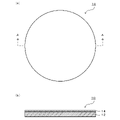
- FIG. 1A and 1B are explanatory views of the laminated structure 10 of the present embodiment, FIG. 1A is a plan view, and FIG. 1B is a sectional view taken along the line AA.
- the laminated structure 10 is a plate-shaped member, and has a semiconductor film 14 on a base substrate 12.
- the plan view figure when the laminated structure 10 is viewed in a plan view is circular in the present embodiment.
- the plan view figure of the laminated structure 10 is not limited to a circle, and may be, for example, a polygon (a quadrangle such as a square or a rectangle, a pentagon, a hexagon, or the like).
- the base substrate 12 is preferably a substrate having a corundum structure, and particularly preferably a substrate oriented in two axes of the c-axis and the a-axis (biaxially oriented substrate).
- the biaxially oriented substrate may be a polycrystal, a mosaic crystal (a set of crystals whose crystal orientations are slightly deviated), or a single crystal.
- the base substrate 12 may be composed of a single material or a solid solution of a plurality of materials as long as it has a corundum structure.
- the base substrate 12 may be a composite base substrate having a layer of a material having a lattice constant closer to ⁇ -Ga 2 O 3 on the base substrate of a material having a corundum structure.
- the composite base substrate for example, (a) a base substrate made of a material having a corundum structure is prepared, and (b) an orientation precursor layer is used using a material whose lattice constant is closer to ⁇ -Ga 2 O 3 than the material of the base substrate. (C) The alignment precursor layer is heat-treated on the base substrate to convert at least the portion near the base substrate into the alignment layer, and if desired, the alignment layer is subjected to (d) grinding, polishing, or the like. It can be manufactured by exposing the surface of the.
- the base substrate 12 is, for example, a sapphire substrate or a layer of an oxide ( ⁇ -Cr 2 O 3 or ⁇ -Fe 2 O 3 or the like) having a lattice constant closer to ⁇ -Ga 2 O 3 than sapphire on one surface of the sapphire substrate.
- a composite base substrate provided with the above.
- the semiconductor film 14 has a corundum-type crystal structure composed of an ⁇ -Ga 2 O 3 or ⁇ -Ga 2 O 3 system solid solution, that is, an ⁇ -Ga 2 O 3 system semiconductor film.
- ⁇ -Ga 2 O 3 belongs to the trigonal crystal group and has a corundum type crystal structure.
- the ⁇ -Ga 2 O 3 system solid solution is a solid solution of other components in ⁇ -Ga 2 O 3 , and the corundum type crystal structure is maintained. Examples of other components include Al 2 O 3 , In 2 O 3 , Cr 2 O 3 , Fe 2 O 3 , Rh 2 O 3 , V 2 O 3 , and Ti 2 O 3 .
- the semiconductor film 14 is warped in a convex or concave shape, and in either case, the amount of warp is within the range of 20 ⁇ m or more and 64 ⁇ m or less, preferably 30 ⁇ m or more and 64 ⁇ m or less, and more preferably 30 ⁇ m or more and 50 ⁇ m or less.
- the fact that the semiconductor film 14 warps in a convex shape means that the film surface of the semiconductor film 14 (base substrate 12) is seen when the cross section of the semiconductor film 14 is cut along the thickness direction. It means that the surface on the opposite side to the side) is convex. As shown in FIGS.
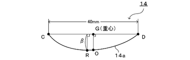
- the fact that the semiconductor film 14 warps in a concave shape means that the film surface of the semiconductor film 14 (base substrate 12 side) when the cross section of the semiconductor film 14 is cut along the thickness direction is viewed. The surface on the opposite side) is concave.
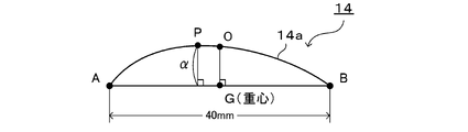
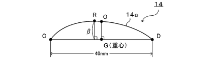
- FIG. 2 in a plan view figure (here, a circle) when the semiconductor film 14 is viewed in a plan view, two straight lines X and Y that pass through a point G which is the center of gravity of the plan view figure and are orthogonal to each other are drawn. Two points A and B 20 mm away from the point G on the straight line X and two points C and D 20 mm away from the point G on the straight line Y are defined. Subsequently, as shown in FIG. 3 when the semiconductor film 14 is warped in a convex shape and FIG.
- the distance between the line segment CD and the point R is defined as the warp amount ⁇ .
- These warp amounts ⁇ and ⁇ are used as the warp amount of the semiconductor film 14.
- the warpage amounts ⁇ and ⁇ are both within the range of 20 ⁇ m or more and 64 ⁇ m or less.
- the smaller value of the warp amount ⁇ and the warp amount ⁇ is preferably 50% or more and 100% or less, and more preferably 85% or more and 100% or less of the larger value.
- the method for measuring the warpage amount ⁇ and ⁇ is not particularly limited, and a known method can be used.
- the warpage amounts ⁇ and ⁇ can be measured using a high-precision laser measuring instrument (LT-9010M manufactured by KEYENCE CORPORATION).
- the warp amount ⁇ can be measured by measuring the distance between the point on the curve AB and the line segment AB at 1 mm intervals between the line segments AB using a high-precision laser measuring device. .. The same applies to the amount of warp ⁇ .
- the length of the line segment PO and the length of the line segment RO is preferably 10 mm or less from the viewpoint of peeling the Ga 2 O 3 semiconductor film without causing cracks.
- These lengths are more preferably 5 mm or less, and even more preferably 3 mm or less.
- the warped shape of the Ga 2 O 3 semiconductor film becomes close to a spherical shape, and the number of places where stress is locally concentrated is reduced, so that cracks are less likely to occur.
- the average film thickness of the semiconductor film 14 is 10 ⁇ m or more, preferably 12 ⁇ m or more, and more preferably 14 ⁇ m or more.
- the upper limit of the average film thickness of the semiconductor film 14 is not particularly limited, but is, for example, 1000 ⁇ m or less.
- the method for measuring the film thickness of the semiconductor film 14 is not particularly limited, and a known method can be used.
- the film thickness of the semiconductor film 14 can be measured using an ellipsometer (M-2000D manufactured by JA Woolam Japan).
- the average film thickness of the semiconductor film 14 is calculated by measuring the film thickness of the semiconductor film 14 at a total of 5 points G, A, B, C, and D in FIG. 2 and calculating the average value as the average film thickness of the semiconductor film 14. can do.
- the area of the film surface of the semiconductor film 14 substantially coincides with the area of the underlying substrate 12.
- the area of the film surface of the semiconductor film 14 is preferably 20 cm 2 or more, more preferably 70 cm 2 or more, and further preferably 170 cm 2 or more. By increasing the area of the semiconductor film 14 in this way, it is possible to obtain a large number of semiconductor elements from one semiconductor film 14, and it is possible to reduce the manufacturing cost.
- the upper limit of the size of the semiconductor film 14 is not particularly limited, but is typically 700 cm 2 or less on one side.
- the semiconductor film 14 can contain a group 14 element as a dopant at a ratio of 1.0 ⁇ 10 16 to 1.0 ⁇ 10 21 / cm 3 .
- the Group 14 element is a Group 14 element according to the periodic table formulated by the IUPAC (International Union of Pure and Applied Chemistry), and specifically, carbon (C), silicon (Si), germanium (Ge), and so on. It is any element of tin (Sn) and lead (Pb).
- the amount of dopant can be appropriately changed according to the desired characteristics, but is preferably 1.0 ⁇ 10 16 to 1.0 ⁇ 10 21 / cm 3 , and more preferably 1.0 ⁇ 10 17 to 1.0. ⁇ 10 19 / cm 3 . It is preferable that these dopants are uniformly distributed in the film and the dopant concentrations on the front surface and the back surface of the semiconductor film 14 are about the same.
- the semiconductor film 14 is preferably an alignment film oriented in a specific plane direction.
- the orientation of the semiconductor film 14 can be investigated by a known method, but it can be investigated by performing reverse pole figure orientation mapping using, for example, an electron backscatter diffraction device (EBSD).
- EBSD electron backscatter diffraction device
- the semiconductor film may be c-axis oriented, or may be c-axis oriented and also oriented in the in-plane direction.
- the method for producing the semiconductor film 14 includes (a) a step of obtaining the laminated structure 10 and (b) a step of peeling the semiconductor film 14 from the base substrate 12.
- the laminated structure 10 is obtained by forming a semiconductor film 14 on a base substrate 12 using an ⁇ -Ga 2 O 3 system material.
- the film forming method is not particularly limited, and a known method can be adopted.
- mist CVD, HVPE, MBE, MOCVD, sputtering, and hydrothermal method are preferable, and mist CVD and HVPE are particularly preferable.
- the convex or concave warp amount of the semiconductor film 14 is within an appropriate range (20 ⁇ m or more and 64 ⁇ m or less), and the average film thickness of the semiconductor film 14 is within an appropriate range (10 ⁇ m or more). ), It is not particularly limited. Further, the amount of convex or concave warpage of the semiconductor film 14 can be appropriately controlled depending on the film forming method, film forming conditions, film thickness and the like.
- a base substrate 12 having a convex warp is used, or the base substrate 12 is convex during film formation. Treatment may be performed so as to cause warpage.
- a method for obtaining such a base substrate 12 for example, a method of preparing a material having a coefficient of thermal expansion higher than that of the base substrate 12 (high thermal expansion material) and forming the material on the back surface of the base substrate 12 at a predetermined temperature is used. Can be mentioned.
- the underlying substrate 12 when the temperature of the high thermal expansion material is lowered from the predetermined temperature at which the film is formed to room temperature, the underlying substrate 12 can be provided with a convex warp due to thermal stress. With respect to the amount of warpage of the base substrate 12, a desired amount of warpage can be realized by controlling the coefficient of thermal expansion and the thickness of the base substrate 12 and the high thermal expansion material, respectively.
- the method for forming a film of a high thermal expansion material is not particularly limited, and examples thereof include AD, HVPE, sputtering, vapor deposition, and CVD, and HVPE, sputtering, and CVD are preferable. Further, instead of forming a film, a high thermal expansion material may be attached to the base substrate at a predetermined temperature.
- the method of pasting is not particularly limited, and examples thereof include a method using an adhesive and a method of sintering. However, it is preferable to form a protective layer on the surface of the base substrate 12 on which the semiconductor film 14 is formed so that the high thermal expansion material does not adhere to and form a film. Examples of such a combination of the base substrate 12 and the high thermal expansion material include sapphire and Cr 2 O 3 single crystal for the underlying substrate 12, and transition metals, Mg Al 2 O 4 and Mg O for the high thermal expansion material.
- the warp amount of the semiconductor film 14 exceeds the appropriate range depending on the film forming method and the film forming conditions
- the warp amount is set within the appropriate range while adopting the film forming method and the film forming conditions.
- a thick base substrate 12 may be used to increase the rigidity, or the thickness of the semiconductor film 14 may be reduced within a range not less than 10 ⁇ m.
- the base substrate 12 having a concave warp may be used, or measures may be taken so that the base substrate 12 has a concave warp during film formation.
- a method for obtaining such a base substrate 12 for example, a method of preparing a material having a coefficient of thermal expansion lower than that of the base substrate 12 (low thermal expansion material) and forming the material on the back surface of the base substrate 12 at a predetermined temperature is used.
- the underlying substrate 12 can be provided with a concave warp due to thermal stress.
- a desired amount of warpage can be realized by controlling the coefficient of thermal expansion and the thickness of the base substrate 12 and the low thermal expansion material, respectively.
- the film forming method of the low thermal expansion material is not particularly limited, and examples thereof include AD, HVPE, sputtering, vapor deposition, and CVD, and HVPE, sputtering, and CVD are preferable.
- a low thermal expansion material may be attached to the base substrate at a predetermined temperature.
- the method of pasting is not particularly limited, and examples thereof include a method using an adhesive and a method of sintering.
- Examples of such a combination of the base substrate 12 and the low thermal expansion material include sapphire and Cr 2 O 3 single crystals as the underlying substrate 12, and metals such as AlN, SiC, W, and Mo as the low thermal expansion material.
- the semiconductor film 14 As another method for reducing the amount of convex warpage of the semiconductor film 14, there is also a method of forming a processed alteration layer on the back surface of the base substrate 12 and reducing the amount of warpage by stress due to the Twiman effect.
- a method for forming the work-altered layer a known method can be used, and examples thereof include grinding and blasting.
- the front surface and the back surface of the base substrate 12 may be ground for the purpose of adjusting the thickness and removing scratches and stains, whereby a processed alteration layer is formed on the base substrate 12, and the base substrate 12 is unintentionally warped. May occur.
- the formed work-altered layer may be removed by, for example, mirror polishing or annealing treatment at a predetermined temperature.
- the thickness equal to or larger than the thickness of the formed work-altered layer may be polished under conditions where the work-altered layer is difficult to be introduced.
- the work-altered layer can be removed by grinding to # 6000 using a grindstone, then performing lap polishing using diamond abrasive grains, and then performing chemical mechanical polishing (CMP) using colloidal silica.
- a base substrate 12 having a concave warp is used, or a concave warp is made on the base substrate 12 during film formation.
- the film forming method and the film forming conditions are adopted.
- a method similar to the above-mentioned method for obtaining the base substrate 12 used to keep the amount of warpage within an appropriate range can be adopted.
- a method for increasing the concave warp amount of the semiconductor film 14 there is also a method of forming a processed alteration layer on the back surface of the base substrate 12 and increasing the warp amount by stress due to the Twiman effect.
- a method for forming the work-altered layer a known method can be used, and examples thereof include grinding and blasting.
- the warp amount of the semiconductor film 14 exceeds the appropriate range depending on the film forming method and the film forming conditions, the warp amount should be kept within the appropriate range while adopting the film forming method and the film forming conditions.
- the rigidity may be increased by using a thick base substrate 12, or the thickness of the semiconductor film 14 may be increased.
- a base substrate 12 having a convex warp may be used, or a treatment may be performed so that the base substrate 12 has a convex warp during film formation.
- FIG. 7 is a schematic cross-sectional view showing the configuration of the mist CVD apparatus 20.
- the mist CVD device 20 includes a mist generator 22, a mist supply pipe 28, and a growth chamber 30.
- the mist generator 22 operates the ultrasonic vibrator 24 provided on the bottom surface to vibrate the raw material solution stored in the mist generator 22 with ultrasonic waves to generate mist.
- a gas introduction port 26 is provided on the side surface of the mist generator 22. The gas introduction port 26 can introduce carrier gas into the mist generator 22 from the outside.
- the mist supply pipe 28 connects the mist generator 22 and the growth chamber 30. The lower end of the mist supply pipe 28 penetrates the ceiling surface of the mist generator 22 and communicates with the inside of the mist generator 22.
- the upper end of the mist supply pipe 28 communicates with the nozzle 32 attached to the floor surface of the growth chamber 30. Therefore, the mist generated in the mist generator 22 is supplied into the growth chamber 30 via the mist supply pipe 28.
- the growth chamber 30 is a cylindrical container, which is provided with a gas discharge port 34 on the upper side surface and a disk-shaped stage 36 on the ceiling surface.
- a base substrate 12 for crystal growth is detachably held on the lower surface of the stage 36.
- a heater 38 for heating the base substrate 12 held on the stage 36 is provided on the ceiling surface of the growth chamber 30.
- a gallium halide solution is prepared as a raw material solution, and the solution is placed in the mist generator 22.
- a sapphire substrate which is ⁇ -Al 2 O 3 , is detachably held on the lower surface of the stage 36 as the base substrate 12.
- the distance d (see FIG. 7) between the upper end of the nozzle 32 and the lower surface of the base substrate 12 is set to an appropriate value (for example, 100 mm or more and 200 mm or less).
- the stage 36 is heated to a desired temperature by the heater 38.
- the mist generator 22 the raw material solution is atomized by the ultrasonic vibrator 24 to generate mist.
- the mist generated by the mist generator 22 passes through the mist supply pipe 28 together with the carrier gas (for example, N 2 or noble gas) introduced from the gas introduction port 26, and the nozzle 32 provided on the floor surface of the growth chamber 30. Is supplied upward from the growth chamber 30 to the inside of the growth chamber 30.
- gallium halide in the raw material solution is thermally decomposed into gallium oxide, which is heteroepitaxially grown on the lower surface of the base substrate 12 to become a semiconductor film 14 ( ⁇ -Ga 2 O 3 system semiconductor film).
- the temperature of the stage 36 is set so that the semiconductor film 14 is formed and the warpage amounts ⁇ and ⁇ of the formed semiconductor film 14 are within the range of 20 ⁇ m or more and 64 ⁇ m or less.
- the laminated structure 10 is obtained. Then, by lowering the temperature of the laminated structure 10 to room temperature (for example, 10 ° C. or higher and 40 ° C. or lower), the laminated structure 10 in which the warp amount and the average film thickness of the semiconductor film 14 are within a desired numerical range can be obtained.
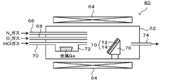
- FIG. 8 is a schematic cross-sectional view showing the configuration of the vapor phase growth apparatus 60 using HVPE.
- the vapor phase growth apparatus 60 includes a reaction vessel 62 and a heater 64.
- the reaction vessel 62 is a vessel made of a material (for example, quartz) that does not react with various raw materials and products.
- a carrier gas supply pipe 66, an oxidation gas supply pipe 68, and a raw material supply pipe 70 are attached to one of the pair of side surfaces of the reaction vessel 62 facing each other, and an exhaust pipe 74 is attached to the other side surface.
- the carrier gas supply pipe 66 supplies a carrier gas (for example, nitrogen, a rare gas, etc.) into the reaction vessel 62.
- the oxidation gas supply pipe 68 supplies oxygen gas as oxidation gas into the reaction vessel 62.
- As the oxidizing gas water vapor, nitrous oxide, or the like may be supplied in addition to oxygen.
- a halogen gas for example, chlorine gas
- a hydrogen halide gas for example, hydrogen chloride gas
- the raw material supply pipe 70 supplies gallium halide gas as a raw material gas into the reaction vessel 62.
- the halogen gas or the hydrogen halide gas may be supplied together with a carrier gas such as nitrogen or a rare gas.
- a susceptor 76 for detachably holding the base substrate 12 is provided downstream of each supply pipe 66, 68, 70 in the reaction vessel 62.
- the exhaust pipe 74 discharges the unreacted gas in the reaction vessel 62.
- a vacuum pump may be connected to the exhaust pipe 74, and the degree of vacuum in the reaction vessel 62 may be adjusted by the vacuum pump. This makes it possible to suppress the gas phase reaction and improve the growth rate distribution.
- the heater 64 is arranged so as to surround the periphery of the reaction vessel 62.
- As the heater 64 for example, a resistance heating type heater or the like can be adopted.
- the oxygen gas supplied from the oxidation gas supply pipe 68 reacts with the raw material gas (gallium halide gas) supplied from the raw material supply pipe 70, and the semiconductor film 14 ( ⁇ -Ga 2 O 3 film) is formed.
- the film formation temperature is set so that the semiconductor film 14 is formed and the warpage amounts ⁇ and ⁇ of the formed semiconductor film 14 are within the range of 20 ⁇ m or more and 64 ⁇ m or less.
- the film formation temperature is preferably 300 ° C. or higher and 800 ° C. or lower, and more preferably 400 ° C. or higher and 700 ° C. or lower.
- the partial pressure of oxygen gas or raw material gas is not particularly limited.
- the partial pressure of the raw material gas may be in the range of 0.05 kPa or more and 10 kPa or less, and the partial pressure of the oxygen gas may be in the range of 0.25 kPa or more and 50 kPa or less.
- the growth time is set so that the average film thickness of the semiconductor film 14 is 10 ⁇ m or more.
- the laminated structure 10 is obtained.
- room temperature for example, 10 ° C. or higher and 40 ° C. or lower
- the laminated structure 10 in which the warp amount and the average film thickness of the semiconductor film 14 are within a desired numerical range can be obtained.
- Step of peeling the semiconductor film 14 from the base substrate 12 The method of peeling the semiconductor film 14 from the base substrate 12 of the room temperature laminated structure 10 obtained as described above is not particularly limited. A known method can be used. Examples of the peeling method include a method of peeling by applying a mechanical impact, a method of peeling by applying heat and utilizing thermal stress, and a method of peeling by applying vibration such as ultrasonic waves. By peeling, the semiconductor film 14 can be obtained as a self-supporting film. Alternatively, the semiconductor film 14 can be reprinted on another support substrate.
- the semiconductor film 14 thus obtained as a self-supporting film preferably has no defects, and preferably has 20 or less cracks per 20 cm 2 film area on the film surface.
- the number of cracks can be counted using, for example, an industrial microscope (ECLIPSE LV150N manufactured by Nikon Corporation).
- the eyepiece is set to 10 times, the objective lens is set to 5 times, the entire film surface is observed in the polarization / differential interference mode, and if cracks are confirmed, the objective lens is changed to 10 times and an image is acquired. You may.
- only cracks having a length of 50 ⁇ m or more are counted as cracks. If the distance from one crack to another is 500 ⁇ m or less, it is regarded as one crack. Regardless of the size of the semiconductor film 14, the number of cracks on the entire surface of the film is measured and converted into the number of cracks per 20 cm 2 of the film area.
- the laminated structure 10 of the present embodiment described above it is possible to suppress the occurrence of cracks and peeling defects during the production of the ⁇ -Ga 2 O 3 system semiconductor film, and by extension, the ⁇ -Ga 2 O 3 system semiconductor.
- the film can be manufactured with good yield.
- the mechanism is not clear, but by keeping the amount of warpage of the semiconductor film 14 within an appropriate range (20 ⁇ m or more and 64 ⁇ m or less), the semiconductor film 14 is in a state where an appropriate stress is applied, and it is easy to peel off from the base substrate 12. Moreover, it is considered that cracks are less likely to occur even if the film is thickened to 10 ⁇ m or more.
- the stress applied to the semiconductor film 14 is insufficient, and the semiconductor film 14 is only partially peeled from the base substrate 12 or cracks when trying to peel with a stronger force. May occur. If the amount of warpage exceeds the upper limit of the appropriate range, the stress applied to the semiconductor film 14 becomes too large, and the semiconductor film 14 on the base substrate 12 may be cracked.
- Example 1 (mist CVD) 1.
- Preparation of Laminated Structure (1) Preparation of Raw Material Solution Metallic Ga was added to hydrochloric acid and stirred at room temperature for 4 weeks to obtain a gallium chloride solution having a gallium ion concentration of 3 mol / L. Water was added to the obtained gallium chloride solution to adjust the aqueous solution so that the gallium ion concentration was 65 mmol / L. Further, ammonium hydroxide was added to adjust the pH to 4.0 to prepare a raw material solution.
- a flow rate control valve (not shown) provided in the gas introduction port 26 is opened to supply the carrier gas to the inside of the mist generator 22 and the growth chamber 30, and the atmosphere of the mist generator 22 and the growth chamber 30 is changed by the carrier gas.
- the flow rate of the carrier gas was adjusted to 1.8 L / min.
- nitrogen gas was used as the carrier gas.
- the raw material solution is atomized by the ultrasonic transducer 24, the generated mist is introduced into the growth chamber 30 by the carrier gas, and the reaction is carried out in the growth chamber 30 to form a circular semiconductor on the lower surface of the base substrate 12.
- the film 14 was formed, and finally the laminated structure 10 was obtained.
- the area of the film surface of the semiconductor film 14 coincided with the area of the base substrate 12.
- the film formation temperature was 520 ° C. and the film formation time was 300 minutes. After that, the temperature of the laminated structure 10 was lowered to room temperature.
- the average film thickness of the semiconductor film 14 was calculated by the method described in the column of [Mode for carrying out the invention]. That is, the film thickness was measured by an ellipsometer (M-2000D manufactured by JA Woolam Japan). The measurement positions were a total of 5 points of points G, A, B, C, and D in FIG. Then, the average value of the film thickness measured at 5 points was taken as the average film thickness. The results are shown in Table 1.
- the eyepiece is set to 10 times, the objective lens is set to 5 times, and the entire film surface is observed in the polarization / differential interference mode. If cracks are confirmed, the objective is used. The lens was changed to 10 times and an image was acquired. Then, only cracks having a length of 50 ⁇ m or more were counted as cracks. Further, when the distance from one crack to another is 500 ⁇ m or less, it is regarded as one crack. Regardless of the size of the semiconductor film 14, the number of cracks on the entire surface of the film was measured and converted into a film area of 20 cm 2 .
- Example 2 (mist CVD) As the base substrate 12, a substrate in which a polycrystalline Al 2 O 3 layer was formed on the back surface of a ⁇ 2-inch c-plane sapphire substrate, the back surface was mirror-finished, and the substrate was warped in a convex shape was used. The method of manufacturing the substrate is shown below.
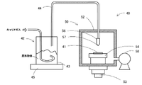
- Al 2 O 3 powder (AKP-20 manufactured by Sumitomo Chemical Co., Ltd.) is used as the raw material powder, and sapphire (diameter 50.8 mm (2 inches), thickness 1.00 mm, c-plane, off-angle 0.2 °) is used as the substrate. Then, an AD film made of Al 2 O 3 was formed on a seed substrate (sapphire substrate) by the AD (aerosol deposition) device 40 shown in FIG.
- the AD device 40 shown in FIG. 9 is configured as a device used in the AD method of injecting raw material powder onto a substrate in an atmosphere having a pressure lower than atmospheric pressure.
- the AD device 40 includes an aerosol generation unit 42 that generates an aerosol of a raw material powder containing a raw material component, and a film forming unit 50 that injects the raw material powder onto a sapphire substrate 41 to form a film containing the raw material component. ..
- the aerosol generation unit 42 includes an aerosol generation chamber 43 that stores raw material powder and receives carrier gas from a gas cylinder (not shown) to generate an aerosol, and a raw material supply pipe 44 that supplies the generated aerosol to the film forming unit 50.
- the aerosol generation chamber 43 and the aerosol in the aerosol are provided with a vibration exciter 45 that applies vibration at a frequency of 10 to 100 Hz.
- the film forming section 50 includes a film forming chamber 52 that injects aerosols onto the sapphire substrate 41, a substrate holder 54 that is arranged inside the film forming chamber 52 and fixes the sapphire substrate 41, and the substrate holder 54 is X-axis-Y-axis. It is equipped with an XY stage 53 that moves in a direction. Further, the film forming section 50 includes an injection nozzle 56 having a slit 57 formed at the tip thereof to inject aerosol into the sapphire substrate 41, and a vacuum pump 58 for reducing the pressure in the film forming chamber 52.
- the AD film formation conditions were as follows. That is, the carrier gas was N 2 , and a ceramic nozzle having a slit having a long side of 5 mm and a short side of 0.3 mm was used.
- the scanning conditions of the nozzle are a scanning speed of 0.5 mm / s, moving 55 mm in the direction perpendicular to the long side of the slit and advancing, moving 5 mm in the direction of the long side of the slit, and perpendicular and returning to the long side of the slit.
- the sapphire substrate on which the AD film was formed was taken out from the AD apparatus and annealed at 1650 ° C. for 4 hours in a nitrogen atmosphere to form a polycrystalline Al 2 O 3 layer on the back surface of the sapphire substrate.
- the substrate thus obtained was fixed to a ceramic surface plate, and the surface on the side on which the AD film was formed was ground to # 6000 using a grindstone to flatten the plate surface.
- the plate surface was smoothed by lapping using diamond abrasive grains. The flatness was improved while the size of the abrasive grains was gradually reduced from 3 ⁇ m to 0.5 ⁇ m.
- CMP chemical mechanical polishing
- the thickness of the polycrystalline Al 2 O 3 layer after mirror finishing was 20 ⁇ m.
- the substrate was fixed to a ceramic surface plate, and the surface of the sapphire substrate was ground to # 6000 using a grindstone to flatten the plate surface.
- the plate surface was smoothed by lapping using diamond abrasive grains. The flatness was improved while the size of the abrasive grains was gradually reduced from 3 ⁇ m to 0.5 ⁇ m.
- a mirror finish was performed by chemical mechanical polishing (CMP) using colloidal silica.
- CMP chemical mechanical polishing
- Example 2 a substrate prepared as described above and warped in a convex shape was used as the base substrate 12, and the film formation was performed by the same method as in Example 1 except that the film formation time was set to 450 minutes. Evaluation was performed. The results are shown in Table 1. From the EDX measurement, it was found that the semiconductor film 14 obtained in Example 2 was also a Ga oxide, and from the EBSD measurement, it was found to be an alignment film having a biaxially oriented corundum-type crystal structure. Moreover, when the total yield was calculated as described above, it was 93%.
- Example 3 (mist CVD) As the base substrate 12, a polycrystalline Al 2 O 3 layer was formed on the back surface of a ⁇ 2-inch c-plane sapphire substrate, and a processed alteration layer was introduced by grinding the back surface to use a substrate that was warped in a convex shape. The method of manufacturing the substrate is shown below.
- Al 2 O 3 powder (AKP-20 manufactured by Sumitomo Chemical Co., Ltd.) is used as the raw material powder, and sapphire (diameter 50.8 mm (2 inches), thickness 1.00 mm, c-plane, off-angle 0.2 °) is used as the substrate. Then, the AD film made of Al 2 O 3 was formed on the seed substrate (sapphire substrate) by the AD apparatus 40 shown in FIG. The AD film forming conditions were the same as in Example 2.
- the sapphire substrate on which the AD film was formed was taken out from the AD apparatus and annealed at 1650 ° C. for 4 hours in a nitrogen atmosphere to form a polycrystalline Al 2 O 3 layer on the back surface of the sapphire substrate.
- the substrate thus obtained was fixed to a ceramic surface plate, and the surface on the side where the AD film was formed was ground to # 325 using a grindstone to introduce a work-altered layer into the polycrystalline Al 2 O 3 layer.
- the thickness of the polycrystalline Al 2 O 3 layer after # 325 grinding was 20 ⁇ m.
- the substrate was fixed to a ceramic surface plate, and the surface of the sapphire substrate was ground to # 6000 using a grindstone to flatten the plate surface.
- the plate surface was smoothed by lapping using diamond abrasive grains.
- the flatness was improved while the size of the abrasive grains was gradually reduced from 3 ⁇ m to 0.5 ⁇ m.
- a mirror finish was performed by chemical mechanical polishing (CMP) using colloidal silica.
- CMP chemical mechanical polishing
- Example 3 the film was formed and evaluated by the same method as in Example 1 except that the substrate 12 produced as described above and warped in a convex shape was used. The results are shown in Table 1. From the EDX measurement, it was found that the semiconductor film 14 obtained in Example 3 was also a Ga oxide, and from the EBSD measurement, it was found to be an alignment film having a biaxially oriented corundum-type crystal structure. Moreover, when the total yield was calculated as described above, it was 85%.
- Example 4 (mist CVD) Examples of the base substrate 12 except that a work-altered layer was introduced by grinding the back surface of a ⁇ 2-inch c-plane sapphire substrate (thickness 0.43 mm) to # 325 and a concavely curved substrate was used. The film formation and evaluation were performed in the same manner as in 1. The results are shown in Table 1. From the EDX measurement, it was found that the semiconductor film 14 obtained in Example 4 was also a Ga oxide, and from the EBSD measurement, it was found to be an alignment film having a biaxially oriented corundum-type crystal structure. Moreover, when the total yield was calculated as described above, it was 76%.
- Example 5 (mist CVD) As the base substrate 12, a processed alteration layer is introduced by blasting the back surface of a ⁇ 2-inch c-plane sapphire substrate (thickness 0.43 mm) with Fujirandom WA (grain number 100 manufactured by Fuji Seisakusho) as an abrasive. The film formation and evaluation were carried out in the same manner as in Example 1 except that the substrate was warped in a concave shape. The results are shown in Table 1. From the EDX measurement, it was found that the semiconductor film 14 obtained in Example 5 was also a Ga oxide, and from the EBSD measurement, it was found to be an alignment film having a biaxially oriented corundum-type crystal structure. Moreover, when the total yield was calculated as described above, it was 92%.
- Example 6 (mist CVD) As the base substrate 12, a substrate that was curved in a concave shape by forming AlN on the back surface of a ⁇ 2-inch c-plane sapphire substrate (thickness 1.00 mm) with HVPE was used. The method of manufacturing the substrate is shown below.
- An AlN film of 5 ⁇ m was formed on the back surface of the sapphire substrate with HVPE at 1200 ° C.
- the substrate was fixed to a ceramic surface plate, and the surface of the sapphire substrate was ground to # 6000 using a grindstone to flatten the plate surface.
- the plate surface was smoothed by lapping using diamond abrasive grains. The flatness was improved while the size of the abrasive grains was gradually reduced from 3 ⁇ m to 0.5 ⁇ m.
- CMP chemical mechanical polishing
- the substrate thickness after polishing was 0.435 mm.
- Example 6 the film was formed and evaluated by the same method as in Example 1 except that the substrate 12 produced as described above and warped in a concave shape was used. The results are shown in Table 1. From the EDX measurement, it was found that the semiconductor film 14 obtained in Example 6 was also a Ga oxide, and from the EBSD measurement, it was found to be an alignment film having a biaxially oriented corundum-type crystal structure. Moreover, when the total yield was calculated as described above, it was 85%.
- Example 7 (mist CVD) As the base substrate 12, a ⁇ 2-inch composite base substrate was used. The method for manufacturing the composite substrate is shown below.
- the AD film formation conditions were as follows. That is, the carrier gas was N 2 , and a ceramic nozzle having a slit having a long side of 5 mm and a short side of 0.3 mm was used.
- the scanning conditions of the nozzle are a scanning speed of 0.5 mm / s, moving 55 mm in the direction perpendicular to the long side of the slit and advancing, moving 5 mm in the direction of the long side of the slit, and perpendicular and returning to the long side of the slit.
- the sapphire substrate on which the AD film was formed was taken out from the AD apparatus and annealed at 1700 ° C. for 4 hours in a nitrogen atmosphere.
- the substrate thus obtained was fixed to a ceramic surface plate, and the surface on the side where the AD film was formed was ground to # 6000 using a grindstone to flatten the plate surface.
- the plate surface was smoothed by lapping using diamond abrasive grains. The flatness was improved while the size of the abrasive grains was gradually reduced from 3 ⁇ m to 0.5 ⁇ m.
- CMP chemical mechanical polishing
- the arithmetic average roughness Ra after processing was 0.1 nm, the amount of grinding and polishing was 50 ⁇ m, and the substrate thickness after polishing was 2.05 mm.
- the surface on the side where the AD film is formed is referred to as a "surface".
- the Cr oxide layer is a layer having a biaxially oriented corundum-type crystal structure that is oriented in the c-axis direction in the normal direction of the substrate and also in the in-plane direction. .. From these, it was shown that an orientation layer made of ⁇ -Cr 2 O 3 was formed on the surface of the substrate. From the above, the manufacturing process of the composite base substrate is schematically shown in FIGS. 10 (a) to 10 (d).
- the a-axis length of the oriented layer was 4.961 ⁇ .
- Example 7 is the same as that of Example 1 except that the film was formed on the ⁇ -Cr 2 O 3 oriented layer of the composite substrate prepared as described above and the film forming time was set to 450 minutes. Film formation and evaluation were performed by the method. The results are shown in Table 1. From the EDX measurement, it was found that the semiconductor film 14 obtained in Example 7 was also a Ga oxide, and from the EBSD measurement, it was found to be an alignment film having a biaxially oriented corundum-type crystal structure. Moreover, when the total yield was calculated as described above, it was 94%.
- Example 8 (HVPE)
- a convexly curved substrate produced by the same method as in Example 2 was prepared as the base substrate 12.
- Hydrogen chloride gas is introduced into the raw material supply pipe 70, metal Ga and hydrogen chloride gas are reacted in the raw material supply pipe 70 to generate gallium chloride gas, and the gallium chloride gas is transferred from the raw material supply pipe 70 into the reaction vessel 62. Supplied.
- oxygen gas was used as the oxidation gas
- N 2 gas was used as the carrier gas.
- the growth temperature was 550 ° C. and the film formation time was 80 minutes. As a result, a laminated structure 10 in which the semiconductor film 14 was formed on the base substrate 12 was obtained.
- Example 8 Subsequent evaluation was performed in the same manner as in Example 1. The results are shown in Table 1. From the EDX measurement, it was found that the semiconductor film 14 obtained in Example 8 was also a Ga oxide, and from the EBSD measurement, it was found to be an alignment film having a biaxially oriented corundum-type crystal structure. Moreover, when the total yield was calculated as described above, it was 93%.
- Comparative Example 1 (Mist CVD) The film formation and evaluation were carried out in the same manner as in Experimental Example 1 except that the film formation time was set to 240 minutes. The results are shown in Table 1. From the EDX measurement, it was found that the semiconductor film 14 obtained in Comparative Example 1 was also a Ga oxide, and from the EBSD measurement, it was found to be an alignment film having a biaxially oriented corundum-type crystal structure. When the total yield of Comparative Example 1 was calculated as described above, it was 59%, which was worse than that of Example 1.
- Al 2 O 3 powder (AKP-20 manufactured by Sumitomo Chemical Co., Ltd.) is used as the raw material powder, and sapphire (diameter 50.8 mm (2 inches), thickness 1.00 mm, c-plane, off-angle 0.2 °) is used as the substrate. Then, the AD film made of Al 2 O 3 was formed on the seed substrate (sapphire substrate) by the AD apparatus 40 shown in FIG. The AD film forming conditions were the same as in Example 2.
- the sapphire substrate on which the AD film was formed was taken out from the AD apparatus and annealed at 1650 ° C. for 4 hours in a nitrogen atmosphere to form a polycrystalline Al 2 O 3 layer on the back surface of the sapphire substrate.
- the substrate thus obtained was fixed to a ceramic surface plate, and the surface on the side on which the AD film was formed was ground to # 6000 using a grindstone to flatten the plate surface.
- the plate surface was smoothed by lapping using diamond abrasive grains. The flatness was improved while the size of the abrasive grains was gradually reduced from 3 ⁇ m to 0.5 ⁇ m.
- CMP chemical mechanical polishing
- the thickness of the polycrystalline Al 2 O 3 layer after the mirror finish was 20 ⁇ m.
- the substrate was fixed to a ceramic surface plate, and the surface of the sapphire substrate was ground to # 6000 using a grindstone to flatten the plate surface.
- the plate surface was smoothed by lapping using diamond abrasive grains. The flatness was improved while the size of the abrasive grains was gradually reduced from 3 ⁇ m to 0.5 ⁇ m.
- a mirror finish was performed by chemical mechanical polishing (CMP) using colloidal silica.
- CMP chemical mechanical polishing
- Comparative Example 2 the film was formed and evaluated by the same method as in Example 1 except that the substrate 12 produced as described above and warped in a convex shape was used. The results are shown in Table 1. From the EDX measurement, it was found that the semiconductor film 14 obtained in Comparative Example 2 was also a Ga oxide, and from the EBSD measurement, it was found to be an alignment film having a biaxially oriented corundum-type crystal structure. When the total yield of Comparative Example 2 was calculated as described above, it was 58%, which was worse than that of Example 1.
- Comparative Example 3 (Mist CVD) As the base substrate 12, a processing alteration layer was introduced by grinding the back surface of a ⁇ 2-inch c-plane sapphire substrate (thickness 0.43 mm) to # 325, and a substrate that was warped in a concave shape was used, and the film formation time was 360 minutes. The film formation and evaluation were carried out in the same manner as in Example 1 except that the above was performed. The results are shown in Table 1. From the EDX measurement, it was found that the semiconductor film 14 obtained in Comparative Example 3 was also a Ga oxide, and from the EBSD measurement, it was found to be an alignment film having a biaxially oriented corundum-type crystal structure. When the total yield of Comparative Example 3 was calculated as described above, it was 58%, which was worse than that of Example 1.
- An AlN film was formed on the back surface of the sapphire substrate with HVPE at 1200 ° C.
- the substrate was fixed to a ceramic surface plate, and the AlN film film formation surface was ground to # 325 using a grindstone to introduce a processed alteration layer.
- the film thickness of AlN after grinding was 5 ⁇ m.
- the surface of the sapphire substrate was ground to # 6000 using a grindstone to flatten the plate surface.
- the plate surface was smoothed by lapping using diamond abrasive grains. The flatness was improved while the size of the abrasive grains was gradually reduced from 3 ⁇ m to 0.5 ⁇ m.
- a mirror finish was performed by chemical mechanical polishing (CMP) using colloidal silica.
- CMP chemical mechanical polishing
- Comparative Example 4 the film was formed and evaluated by the same method as in Example 1 except that the substrate 12 produced as described above and warped in a concave shape was used. The results are shown in Table 1. From the EDX measurement, it was found that the semiconductor film 14 obtained in Comparative Example 4 was also a Ga oxide, and from the EBSD measurement, it was found to be an alignment film having a biaxially oriented corundum-type crystal structure. When the total yield of Comparative Example 4 was calculated as described above, it was 59%, which was worse than that of Example 1.
- the present invention can be used, for example, as a material for a power semiconductor.
Landscapes
- Chemical & Material Sciences (AREA)
- Metallurgy (AREA)
- Organic Chemistry (AREA)
- Engineering & Computer Science (AREA)
- Materials Engineering (AREA)
- Crystallography & Structural Chemistry (AREA)
- Inorganic Chemistry (AREA)
- General Chemical & Material Sciences (AREA)
- Chemical Kinetics & Catalysis (AREA)
- Mechanical Engineering (AREA)
- Dispersion Chemistry (AREA)
- Crystals, And After-Treatments Of Crystals (AREA)
- Recrystallisation Techniques (AREA)
Abstract
Description
(a)ミストCVD法又はHVPE法を用いて300℃以上800℃以下の温度で下地基板上にα-Ga2O3又はα-Ga2O3系固溶体からなるコランダム型結晶構造を有する半導体膜を形成し、その後温度を室温まで下げることにより、上述した積層構造体を得る工程と、
(b)前記積層構造体の前記半導体膜を前記下地基板から剥離することにより前記半導体膜を得る工程と、
を含むものとしてもよい。
図1は、本実施形態の積層構造体10の説明図であり、(a)は平面図、(b)はA-A断面図である。
半導体膜14の製法には、(a)積層構造体10を得る工程と、(b)半導体膜14を下地基板12から剥離する工程とが含まれる。
積層構造体10は、下地基板12上にα-Ga2O3系材料を用いて半導体膜14を成膜することにより得られる。成膜方法は、特に限定されるものではなく、公知の手法が採用可能である。成膜方法としては、ミストCVD、HVPE、MBE、MOCVD、スパッタリング、水熱法が好ましく、ミストCVD、HVPEが特に好ましい。
上述のようにして得られた室温の積層構造体10の下地基板12から半導体膜14を剥離する方法は、特に限定されるものではなく、公知の方法を用いることができる。剥離方法としては、例えば、機械的衝撃を加えて剥離する方法、熱を加えて熱応力を利用して剥離する方法、超音波等の振動を加えて剥離する方法などが挙げられる。剥離によって、半導体膜14を自立膜として得ることができる。あるいは、半導体膜14を別の支持基板に転載することもできる。
1.積層構造体の作製
(1)原料溶液の作製
塩酸に金属Gaを添加し、室温で4週間撹拌することでガリウムイオン濃度が3mol/Lとなる塩化ガリウム溶液を得た。得られた塩化ガリウム溶液に水を加えてガリウムイオン濃度が65mmol/Lとなるように水溶液を調整した。更に水酸化アンモニウムを添加して、pHを4.0となるように調整し、原料溶液とした。
図7に示した構成を有するミストCVD装置20において、上記(1)の原料溶液をミスト発生器22内に収容した。次に、下地基板12としてφ2インチ(面積20.3cm2)のc面サファイア基板(厚さ0.43mm)をセットし、ノズル32の上端と下地基板12の下面との間の距離dを150mmとした。ヒータ38により、ステージ36の温度を520℃まで昇温させ、温度安定化のため30分保持した。次に、ガス導入口26に備えられた図示しない流量調節弁を開いてキャリアガスをミスト発生器22及び成長室30の内部に供給し、ミスト発生器22及び成長室30の雰囲気をキャリアガスで十分置換した後、キャリアガスの流量を1.8L/minに調節した。ここでは、キャリアガスとして窒素ガスを用いた。
超音波振動子24によって原料溶液を霧化し、発生したミストをキャリアガスによって成長室30内に導入し、成長室30内で反応させることで下地基板12の下面に円形の半導体膜14を形成し、最終的に積層構造体10を得た。半導体膜14の膜表面の面積は、下地基板12の面積と一致した。成膜温度は520℃、成膜時間は300分であった。その後、積層構造体10の温度を室温まで下げた。
(1)表面EDX
得られた膜の表面のEDX測定を実施した結果、Ga、Oのみが検出された。これにより、得られた半導体膜14はGa酸化物であることが分かった。
半導体膜14のEBSD測定を行った。得られた逆極点図方位マッピングから、半導体膜14は基板法線方向にc軸配向、面内方向にも配向した二軸配向のコランダム型結晶構造を有することが分かった。これらより、α-Ga2O3からなる配向膜が形成されていることが示された。
[発明を実施するための形態]の欄に記載の方法にて半導体膜14の反り量α、反り量β、線分POの長さ及び線分ROの長さを測定した。その結果を表1に示す。表1には、反り量の大小割合(反り量α,βのうち大きい方の値に対する小さい方の割合)も示した。
[発明を実施するための形態]の欄に記載の方法にて半導体膜14の平均膜厚を算出した。すなわち、膜厚の測定は、エリプソメータ―(ジェー・エー・ウーラム・ジャパン製M-2000D)によって行った。測定位置は、図2の点G,A,B,C,Dの合計5点とした。そして、5点で測定した膜厚の平均値を平均膜厚とした。その結果を表1に示す。
積層構造体10の半導体膜14を超音波振動(周波数45kHz)により下地基板12から剥離した。完全に剥離したものを良品、剥離しなかったものや一部しか剥離しなかったものを不良品とし、剥離歩留まり[%]=剥離良品数/(剥離良品数+剥離不良品数)×100の式より剥離歩留まりを算出した。剥離歩留まり結果を表1に示す。また、剥離した後の半導体膜14(ただし、剥離良品のみ)について、[発明を実施するための形態]の欄で述べた方法によりクラックを観察し、クラック歩留まりを評価した。すなわち、工業用顕微鏡(ニコン製ECLIPSE LV150N)を用いて、接眼レンズを10倍、対物レンズを5倍とし、偏光・微分干渉モードにて膜表面全体を観察し、クラックが確認された場合は対物レンズを10倍に変更し、画像を取得した。そして、長さ50μm以上のクラックのみ、クラックとしてカウントした。また、あるクラックから別のクラックまでの距離が500μm以下の場合は一つのクラックとみなした。半導体膜14のサイズに関わらず、膜表面の全面でのクラック数を計測し、膜面積20cm2当たりに換算した。膜面積20cm2当たりのクラック数が20個以下を良品、それ以外を不良品とし、クラック歩留まり[%]=クラック良品数/(クラック良品数+クラック不良品数)×100の式よりクラック歩留まりを算出した。クラック歩留まり結果を表1に示す。そして、総合歩留まり[%]=剥離歩留まり×クラック歩留まり/100の式より総合歩留まりを算出したところ、75%であった。
下地基板12として、φ2インチのc面サファイア基板の裏面に多結晶のAl2O3層を形成し、裏面を鏡面仕上げにして凸状に反った基板を用いた。基板の作製方法を下記に示す。
下地基板12として、φ2インチのc面サファイア基板の裏面に多結晶のAl2O3層を形成し、裏面を研削することで加工変質層を導入して凸状に反った基板を用いた。基板の作製方法を下記に示す。
下地基板12として、φ2インチのc面サファイア基板(厚さ0.43mm)の裏面を#325まで研削することにより加工変質層を導入して凹状に反った基板を用いたこと以外は、実施例1と同様の方法で成膜・評価を行った。結果を表1に示す。実施例4で得られた半導体膜14も、EDX測定からGa酸化物であること、EBSD測定から二軸配向のコランダム型結晶構造を有する配向膜であることが分かった。また、上述のように総合歩留まりを算出したところ76%であった。
下地基板12として、φ2インチのc面サファイア基板(厚さ0.43mm)の裏面を研磨材としてフジランダムWA(粒番号100 不二製作所製)を用いてブラスト処理することにより加工変質層を導入して凹状に反った基板を用いたこと以外は、実施例1と同様の方法で成膜・評価を行った。結果を表1に示す。実施例5で得られた半導体膜14も、EDX測定からGa酸化物であること、EBSD測定から二軸配向のコランダム型結晶構造を有する配向膜であることが分かった。また、上述のように総合歩留まりを算出したところ92%であった。
下地基板12として、φ2インチのc面サファイア基板(厚さ1.00mm)の裏面にHVPEにてAlNを成膜することにより凹状に反った基板を用いた。基板の作製方法を下記に示す。
下地基板12として、φ2インチの複合下地基板を用いた。複合下地基板の作製方法を以下に示す。
原料粉体としてCr2O3粉体(ランクセス製 カラーサームグリーン)、基板としてサファイア(直径50.8mm(2インチ)、厚さ2.00mm、c面、オフ角0.2°)を用いて、図9に示されるAD装置40により種基板(サファイア基板)上にCr2O3からなるAD膜(配向前駆体層)を形成した。
(2a)断面EDX
エネルギー分散型X線分析器(EDX)を用いて基板主面に直交する断面の組成分析を実施した。その結果、複合下地基板の表面から深さ約20μmまでの範囲ではCr、Oのみが検出された。Cr、Oの比率は約20μmの範囲ではほぼ変化がなく、約20μmの厚みを有するCr酸化物層が形成されていることが分かった。また、そのCr酸化物層から更に深さ30μmまで範囲ではCr、O、Alが検出され、Cr酸化物層とサファイア基板の間に約30μmのCr・Al酸化物層(傾斜組成層)を形成していることが分かった。Cr・Al酸化物層内ではCrとAlの比率が異なり、サファイア基板側ではAl濃度が高く、Cr酸化物層に近い側ではAl濃度が低下している様子が認められた。
電子線後方散乱回折装置(EBSD)(オックスフォード・インストゥルメンツ社製Nordlys Nano)を取り付けたSEM(日立ハイテクノロジーズ社製、SU-5000)にてCr酸化物層で構成される基板表面の逆極点図方位マッピングを500μm×500μmの視野で実施した。このEBSD測定の諸条件は以下のとおりとした。
・加速電圧:15kV
・スポット強度:70
・ワーキングディスタンス:22.5mm
・ステップサイズ:0.5μm
・試料傾斜角:70°
・測定プログラム: Aztec (version 3.3)
多機能高分解能X線回折装置(ブルカー・エイエックスエス株式会社製、D8 DISCOVER)を用いて基板表面のXRDインプレーン測定を行った。具体的には基板表面の高さに合わせてZ軸を調整した後、(11-20)面に対してChi、Phi、ω、2θを調整して軸立てを行い、以下の条件にて2θ-ω測定を行った。
・管電圧:40kV
・管電流:40mA
・検出器:Tripple Ge(220) Analyzer
・Ge(022)非対称反射モノクロメーターにて平行単色光化(半値幅28秒)したCuKα線
・ステップ幅:0.001°
・スキャンスピード:1.0秒/ステップ
図8に示した気相成長装置60において、下地基板12として実施例2と同様の方法で作製した凸状に反った基板を準備した。原料供給管70に塩化水素ガスを導入し、原料供給管70内で金属Gaと塩化水素ガスを反応させて塩化ガリウムガスを生成し、その塩化ガリウムガスを原料供給管70から反応容器62内に供給した。また、酸化ガスとして酸素ガスを用い、キャリアガスとしてN2ガスを用いた。成長温度は550℃とし、成膜時間は80分とした。これにより、下地基板12に半導体膜14が形成された積層構造体10を得た。その後の評価は実施例1と同様の方法で行った。結果を表1に示す。実施例8で得られた半導体膜14も、EDX測定からGa酸化物であること、EBSD測定から二軸配向のコランダム型結晶構造を有する配向膜であることが分かった。また、上述のように総合歩留まりを算出したところ93%であった。
成膜時間を240分にしたこと以外は、実験例1と同様の方法で成膜・評価を行った。結果を表1に示す。比較例1で得られた半導体膜14も、EDX測定からGa酸化物であること、EBSD測定から二軸配向のコランダム型結晶構造を有する配向膜であることが分かった。比較例1の総合歩留まりを上述のように算出したところ59%であり、実施例1と比較して総合歩留まりが悪かった。
下地基板12として、φ2インチのc面サファイア基板の裏面に多結晶のAl2O3層を形成し、裏面を鏡面仕上げにして凸状に反った基板を用いた。基板の作製方法を下記に示す。
下地基板12として、φ2インチのc面サファイア基板(厚さ0.43mm)の裏面を#325まで研削することにより加工変質層を導入して凹状に反った基板を用い、成膜時間を360分にしたこと以外は、実施例1と同様の方法で成膜・評価を行った。結果を表1に示す。比較例3で得られた半導体膜14も、EDX測定からGa酸化物であること、EBSD測定から二軸配向のコランダム型結晶構造を有する配向膜であることが分かった。比較例3の総合歩留まりを上述のように算出したところ58%であり、実施例1と比較して総合歩留まりが悪かった。
下地基板12として、φ2インチのc面サファイア基板(厚さ1.00mm)の裏面にHVPEにてAlNを成膜し、その後研削することによりAlN膜に加工変質層を導入して凹状に反った基板を用いたこと以外は、実施例1と同様の方法で成膜・評価を行った。基板の作製方法を下記に示す。

Claims (5)
- 下地基板上にα-Ga2O3又はα-Ga2O3系固溶体からなるコランダム型結晶構造を有する半導体膜を備えた積層構造体であって、
前記半導体膜の平均膜厚が10μm以上であり、前記半導体膜は凸状又は凹状に反っており、前記半導体膜の反り量が20μm以上64μm以下である、
積層構造体。 - 前記半導体膜を平面視したときの平面視図形において、前記平面視図形の重心である点Gを通り互いに直交する2つの直線X,Yを引き、直線X上で点Gからそれぞれ20mm離れた2点A,Bと直線Y上で点Gからそれぞれ20mm離れた2点C,Dとを定め、前記半導体膜の表面における点Aと点Bとの間の曲線AB上の任意の点のうち線分ABまでの距離が最長となる点Pを定め、前記半導体膜の表面における点Cと点Dとの間の曲線CD上の任意の点のうち線分CDまでの距離が最長となる点Rを定め、線分ABと点Pとの距離を反り量α、線分CDと点Rとの距離を反り量βとしたとき、前記反り量α,βを前記半導体膜の反り量とする、
請求項1に記載の積層構造体。 - 前記半導体膜の表面において点Gに対応する点Oを定めたとき、線分POの長さ及び線分ROの長さが10mm以下である、
請求項2に記載の積層構造体。 - 前記反り量α,βのうち小さい方の値が大きい方の値の50%以上100%以下である、
請求項2又は3に記載の積層構造体。 - 前記半導体膜の反り量が30μm以上64μm以下である、
請求項1~4のいずれか1項に記載の積層構造体。
Priority Applications (3)
| Application Number | Priority Date | Filing Date | Title |
|---|---|---|---|
| CN202180054549.7A CN116018260B (zh) | 2020-09-24 | 2021-06-09 | 层叠结构体 |
| JP2022551143A JPWO2022064783A1 (ja) | 2020-09-24 | 2021-06-09 | |
| US18/181,636 US12563795B2 (en) | 2020-09-24 | 2023-03-10 | Multilayer structure |
Applications Claiming Priority (2)
| Application Number | Priority Date | Filing Date | Title |
|---|---|---|---|
| JP2020159611 | 2020-09-24 | ||
| JP2020-159611 | 2020-09-24 |
Related Child Applications (1)
| Application Number | Title | Priority Date | Filing Date |
|---|---|---|---|
| US18/181,636 Continuation US12563795B2 (en) | 2020-09-24 | 2023-03-10 | Multilayer structure |
Publications (1)
| Publication Number | Publication Date |
|---|---|
| WO2022064783A1 true WO2022064783A1 (ja) | 2022-03-31 |
Family
ID=80846351
Family Applications (1)
| Application Number | Title | Priority Date | Filing Date |
|---|---|---|---|
| PCT/JP2021/021939 Ceased WO2022064783A1 (ja) | 2020-09-24 | 2021-06-09 | 積層構造体 |
Country Status (4)
| Country | Link |
|---|---|
| US (1) | US12563795B2 (ja) |
| JP (1) | JPWO2022064783A1 (ja) |
| CN (1) | CN116018260B (ja) |
| WO (1) | WO2022064783A1 (ja) |
Cited By (1)
| Publication number | Priority date | Publication date | Assignee | Title |
|---|---|---|---|---|
| EP4306676A4 (en) * | 2021-03-12 | 2025-02-19 | Shin-Etsu Chemical Co., Ltd. | SEMICONDUCTOR ARRANGEMENT |
Families Citing this family (1)
| Publication number | Priority date | Publication date | Assignee | Title |
|---|---|---|---|---|
| WO2021048950A1 (ja) * | 2019-09-11 | 2021-03-18 | 日本碍子株式会社 | 半導体膜 |
Citations (3)
| Publication number | Priority date | Publication date | Assignee | Title |
|---|---|---|---|---|
| JP2016013932A (ja) * | 2014-06-30 | 2016-01-28 | 株式会社タムラ製作所 | Ga2O3系単結晶基板 |
| JP2016157878A (ja) * | 2015-02-25 | 2016-09-01 | 株式会社Flosfia | 結晶性酸化物半導体膜、半導体装置 |
| WO2020194763A1 (ja) * | 2019-03-28 | 2020-10-01 | 日本碍子株式会社 | 半導体膜 |
Family Cites Families (3)
| Publication number | Priority date | Publication date | Assignee | Title |
|---|---|---|---|---|
| CN110676303A (zh) * | 2014-07-22 | 2020-01-10 | 株式会社Flosfia | 结晶性半导体膜和板状体以及半导体装置 |
| JP2017214232A (ja) * | 2016-05-30 | 2017-12-07 | パナソニックIpマネジメント株式会社 | 窒化物化合物半導体基板の製造方法 |
| KR20230048008A (ko) * | 2020-08-06 | 2023-04-10 | 신에쓰 가가꾸 고교 가부시끼가이샤 | 반도체 적층체, 반도체 소자 및 반도체 소자의 제조방법 |
-
2021
- 2021-06-09 WO PCT/JP2021/021939 patent/WO2022064783A1/ja not_active Ceased
- 2021-06-09 JP JP2022551143A patent/JPWO2022064783A1/ja active Pending
- 2021-06-09 CN CN202180054549.7A patent/CN116018260B/zh active Active
-
2023
- 2023-03-10 US US18/181,636 patent/US12563795B2/en active Active
Patent Citations (3)
| Publication number | Priority date | Publication date | Assignee | Title |
|---|---|---|---|---|
| JP2016013932A (ja) * | 2014-06-30 | 2016-01-28 | 株式会社タムラ製作所 | Ga2O3系単結晶基板 |
| JP2016157878A (ja) * | 2015-02-25 | 2016-09-01 | 株式会社Flosfia | 結晶性酸化物半導体膜、半導体装置 |
| WO2020194763A1 (ja) * | 2019-03-28 | 2020-10-01 | 日本碍子株式会社 | 半導体膜 |
Cited By (1)
| Publication number | Priority date | Publication date | Assignee | Title |
|---|---|---|---|---|
| EP4306676A4 (en) * | 2021-03-12 | 2025-02-19 | Shin-Etsu Chemical Co., Ltd. | SEMICONDUCTOR ARRANGEMENT |
Also Published As
| Publication number | Publication date |
|---|---|
| CN116018260B (zh) | 2025-08-05 |
| US20230231013A1 (en) | 2023-07-20 |
| US12563795B2 (en) | 2026-02-24 |
| CN116018260A (zh) | 2023-04-25 |
| JPWO2022064783A1 (ja) | 2022-03-31 |
Similar Documents
| Publication | Publication Date | Title |
|---|---|---|
| JP7461851B2 (ja) | 半導体膜 | |
| CN113574214B (zh) | 基底基板及其制造方法 | |
| KR101749781B1 (ko) | 단결정 기판, 이를 이용하여 얻어지는 ⅲ족 질화물 결정 및 ⅲ족 질화물 결정의 제조방법 | |
| US12159907B2 (en) | Semiconductor film | |
| JP7410009B2 (ja) | 半導体膜 | |
| JP7644812B2 (ja) | 複合基板、複合基板の製法及び酸化ガリウム結晶膜の製法 | |
| US12563795B2 (en) | Multilayer structure | |
| JP7439117B2 (ja) | 下地基板及びその製造方法 | |
| WO2021048950A1 (ja) | 半導体膜 | |
| WO2020195355A1 (ja) | 下地基板 | |
| JP7320070B2 (ja) | 下地基板及びその製造方法 | |
| WO2020261356A1 (ja) | 半導体膜 | |
| JP6094243B2 (ja) | 複合基板およびそれを用いた半導体ウエハの製造方法 |
Legal Events
| Date | Code | Title | Description |
|---|---|---|---|
| 121 | Ep: the epo has been informed by wipo that ep was designated in this application |
Ref document number: 21871916 Country of ref document: EP Kind code of ref document: A1 |
|
| ENP | Entry into the national phase |
Ref document number: 2022551143 Country of ref document: JP Kind code of ref document: A |
|
| NENP | Non-entry into the national phase |
Ref country code: DE |
|
| 122 | Ep: pct application non-entry in european phase |
Ref document number: 21871916 Country of ref document: EP Kind code of ref document: A1 |
|
| WWG | Wipo information: grant in national office |
Ref document number: 202180054549.7 Country of ref document: CN |