WO2022060171A1 - Iii족 및 v족 원소를 포함하는 할로겐 원소 도핑 나노클러스터 및 이의 제조방법 - Google Patents
Iii족 및 v족 원소를 포함하는 할로겐 원소 도핑 나노클러스터 및 이의 제조방법 Download PDFInfo
- Publication number
- WO2022060171A1 WO2022060171A1 PCT/KR2021/012828 KR2021012828W WO2022060171A1 WO 2022060171 A1 WO2022060171 A1 WO 2022060171A1 KR 2021012828 W KR2021012828 W KR 2021012828W WO 2022060171 A1 WO2022060171 A1 WO 2022060171A1
- Authority
- WO
- WIPO (PCT)
- Prior art keywords
- nanoclusters
- doped
- inp
- halogen
- precursor
- Prior art date
- Legal status (The legal status is an assumption and is not a legal conclusion. Google has not performed a legal analysis and makes no representation as to the accuracy of the status listed.)
- Ceased
Links
Images




Classifications
-
- C—CHEMISTRY; METALLURGY
- C09—DYES; PAINTS; POLISHES; NATURAL RESINS; ADHESIVES; COMPOSITIONS NOT OTHERWISE PROVIDED FOR; APPLICATIONS OF MATERIALS NOT OTHERWISE PROVIDED FOR
- C09K—MATERIALS FOR MISCELLANEOUS APPLICATIONS, NOT PROVIDED FOR ELSEWHERE
- C09K11/00—Luminescent materials, e.g. electroluminescent or chemiluminescent
- C09K11/02—Use of particular materials as binders, particle coatings or suspension media therefor
-
- C—CHEMISTRY; METALLURGY
- C09—DYES; PAINTS; POLISHES; NATURAL RESINS; ADHESIVES; COMPOSITIONS NOT OTHERWISE PROVIDED FOR; APPLICATIONS OF MATERIALS NOT OTHERWISE PROVIDED FOR
- C09K—MATERIALS FOR MISCELLANEOUS APPLICATIONS, NOT PROVIDED FOR ELSEWHERE
- C09K11/00—Luminescent materials, e.g. electroluminescent or chemiluminescent
- C09K11/02—Use of particular materials as binders, particle coatings or suspension media therefor
- C09K11/025—Use of particular materials as binders, particle coatings or suspension media therefor non-luminescent particle coatings or suspension media
-
- B—PERFORMING OPERATIONS; TRANSPORTING
- B82—NANOTECHNOLOGY
- B82Y—SPECIFIC USES OR APPLICATIONS OF NANOSTRUCTURES; MEASUREMENT OR ANALYSIS OF NANOSTRUCTURES; MANUFACTURE OR TREATMENT OF NANOSTRUCTURES
- B82Y40/00—Manufacture or treatment of nanostructures
Definitions
- the present invention relates to a halogen element-doped nanocluster containing a group III and V element and a method for preparing the same, and more particularly, a reaction between a precursor nanocluster containing a group III element and a group V element and a halogen precursor compound It relates to halogen element-doped nanoclusters prepared through
- Nanoclusters or superatoms composed of a specific number of metal atoms and ligands follow the macroatomic orbital theory, in which the valence electrons of particles are newly defined, and this theory is regarded as one giant atom. am.
- Nanoclusters are more stable than single atoms or nanoparticles, and have stronger molecular properties than metallic properties, so they have completely different optical and electrochemical properties from nanoparticles.
- optical, electrical and catalytic properties of nanoclusters are sensitively changed according to the number of metal atoms, types of metal atoms, ligands, etc., research on nanoclusters is being actively conducted in a wide variety of fields.
- Semiconductor nanoparticles have high luminous efficiency and have superior durability against photobleaching compared to organic dye materials.
- a wide range of emission wavelengths from visible to near infrared rays can be obtained, and in particular, various emission colors with narrow color purity can be realized by selectively controlling the size of semiconductor nanoparticles.
- Research is being actively conducted to apply the excellent optical properties of semiconductor nanoparticles to industrial and medical fields such as displays, solar cells, and bioimaging.
- optical properties such as full-width at half-maximum (FWHM), quantum efficiency, blinking of light emission, and photostability in the emission spectrum are important.
- group II-VI semiconductor nanoparticles based on cadmium chalcogenide which is an ion-binding material, it has excellent optical properties such as a narrow full width at half maximum of light emission and high quantum efficiency. there is a limit there.
- group III-V based semiconductor nanoparticles In order to overcome the risk of biotoxicity caused by heavy metal contamination, the development of group III-V based semiconductor nanoparticles using non-metallic materials has been in progress.
- biotoxicity is low and the emission wavelength band is in the visible light region, so it is emerging as a material replacing cadmium chalcogenide nanoparticles.
- group III-V-based InP nanoparticles in the process of finding a balance point between the bonding enthalpy and surface energy in the crystal, it passes through various paths in a non-equilibrium state, thereby obtaining heterogeneous particles and controlling the shape of the particles. It shows limitations and is subject to many restrictions in terms of application.
- nanoparticles having a higher size homogeneity can be synthesized than using a molecular precursor, which is a general nanoparticle synthesis precursor.
- semiconductor nanoclusters when semiconductor nanoclusters are applied as synthetic precursors, it is possible to develop semiconductor nanostructures having various shapes such as nanorods, nanowires, and nanobelts. Since semiconductor nanostructures of various shapes exhibit excellent electrical, optical, mechanical, and thermal properties, they can be applied to devices such as chemical and biological sensors, field effect transistors, and light emitting diodes. For example, in the case of a one-dimensional nanostructure manufactured by using a semiconductor nanocluster as a precursor, it has various advantages due to unique optical properties such as polarization.
- Group III-V semiconductor nanoclusters have better applicability than Group II-VI semiconductor nanoclusters, and provide more diverse derivatives in the field of devices such as chemical and biological sensors, field effect transistors, and light emitting diodes. It can be used as a very useful material.
- an object of the present invention is to provide a halogen element-doped nanocluster containing group III and group V elements and a method for manufacturing the same. More specifically, to provide a halogen element-doped nanoclusters through the reaction of a precursor nanoclusters containing a group III element and a group V element with a halogen precursor compound, and nanoclusters having various halogen doping contents and a method for manufacturing the same. there is.
- the present invention for achieving the above object includes a group III element and a group V element, and provides a halogen element doped nanoclusters represented by the following formula (1).
- x is an integer from 20 to 60
- y is an integer from 4 to 36
- z is an integer from 10 to 120
- k is an integer from 2 to 50
- M 1 is a group III element
- M 2 is a group V element
- X is a halogen atom
- L is a ligand of alkylcarboxyl, alkenylcarboxyl, alkylcarbonyl, alkenylcarbonyl, alkyloxy, alkenyloxy or aryloxy.
- the halogen element-doped nanoclusters may have a maximum absorption wavelength at 368 nm, and X may be Br.
- the halogen element-doped nanoclusters may have a maximum absorption wavelength at 376 nm, and X may be I.
- the halogen element-doped nanoclusters may be derived from precursor nanoclusters having a maximum absorption wavelength at 386 nm.
- M 1 may be In, and M 2 may be P.
- the precursor nanoclusters may be In 37 P 20 (O 2 CR) 51 .
- R stands for (C1-C20)alkyl or (C2-C2-)alkenyl
- the halogen element-doped nanocluster may have a polytwistane structure.
- the halogen element-doped nanoclusters may have a diameter of 1 to 3 nm.
- halogen-doped nanoparticles may be prepared from the halogen-doped nanoclusters.
- the present invention also provides a method for manufacturing a halogen element-doped nanoclusters, comprising: a first step of preparing a precursor nanoclusters including a group III element and a group V element; A second step of preparing a reaction solution by mixing the precursor nanoclusters with M 1 X 3 solution; and a third step of heating and reacting the reaction solution.
- the preparing of the precursor nanoclusters including the group III element and the group V element includes mixing and reacting M 1 (C2-C4 alkylcarboxyl) 3 , C6-C16 fatty acid and a phosphine precursor compound. may be doing
- the heating temperature in the third step may be 20 to 170 °C.
- M 1 X 3 molecules may be added in an excessive amount with respect to the precursor nanocluster molecules.
- the present invention it is possible to provide a halogen element-doped nanocluster containing a group III and group V element and a method for manufacturing the same. More specifically, the halogen element-doped nanoclusters containing group III and V elements according to the present invention belong to 2 nm or less, and the molecular structure corresponds to a thermodynamic local point and thus has a particularly stable structure despite its small size. This is the structure of a magic-size cluster (MSC) that exists as
- the precursor nanoclusters containing a group III element and a group V element have various halogen doping contents by controlling the reaction conditions of the halogen precursor compound and the precursor nanoclusters containing the group III element and the group V element. It is possible to provide nanoclusters having a maximum absorption wavelength different from the maximum absorption wavelength.
- nanoparticles with uniform size homogeneity and physicochemical properties are synthesized with high reproducibility than using a molecular precursor, which is a general nanoparticle synthesis precursor.
- a molecular precursor which is a general nanoparticle synthesis precursor.
- it can be preferably used as a precursor that can freely control the shape of the nanoparticles.
- anisotropic nanoparticles using halogen element-doped nanoclusters as precursors chemical and biological sensors, field effect transistors, and light emitting diodes have excellent electrical, optical, mechanical and thermal properties of anisotropic nanoparticles. It can be preferably applied in the device field, such as, and has the potential to implement differentiated physicochemical properties compared to the conventional semiconductor nanoparticles of group III and V elements as the halogen element is doped.
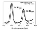
- 3 is a TEM image of 386-InP MSCs and F368-InP:Br nanoclusters.
- FIG. 9 is an absorption spectrum of a growth process in which F376-InP:I nanoclusters were chemically converted and synthesized using 386-InP MSCs and 28 equivalents of InI 3 by raising the temperature from room temperature to 150° C.
- FIG. 9 is an absorption spectrum of a growth process in which F376-InP:I nanoclusters were chemically converted and synthesized using 386-InP MSCs and 28 equivalents of InI 3 by raising the temperature from room temperature to 150° C.
- 10 is a TEM image of 386-InP MSCs and F376-InP:I nanoclusters.
- 11 is an XRD pattern of 386-InP MSCs and F376-InP:I nanoclusters.
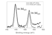
- 13 is an In 3d 3/2 XPS spectrum of 386-InP MSCs and F376-InP:I nanoclusters.
- the numerical value of the maximum absorption wavelength may include an error range of ⁇ 2% of the maximum absorption wavelength value.
- nanocluster is used synonymously with superatom or magic-size cluster (MSC).
- nanoparticles can be synthesized using nanoclusters as a precursor for nanoparticle synthesis, and research was intensified. By confirming that it can be doped with the content, the present invention was completed.
- the halogen element-doped nanoclusters containing group III and V elements according to the present invention can be preferably used as a synthesis precursor of nanoparticles, and nanoparticles having uniform size homogeneity and physicochemical properties of nanoparticles have high reproducibility. can be synthesized.
- the anisotropic nanoparticles can have excellent electrical, optical, mechanical and thermal properties, and as the halogen element is doped, conventional III It is possible to implement different physicochemical properties compared to semiconductor nanoparticles of group and V elements.
- the halogen element-doped nanoclusters according to the present invention are characterized in that they are nanoclusters satisfying Chemical Formula 1.
- x is an integer from 20 to 60
- y is an integer from 4 to 36
- z is an integer from 10 to 120
- k is an integer from 2 to 50
- M 1 is a group III element
- M 2 is a group V Element
- X is a halogen atom
- L is a ligand of alkylcarboxyl, alkenylcarboxyl, alkylcarbonyl, alkenylcarbonyl, alkyloxy, alkenyloxy or aryloxy.
- L is C2-C20 alkylcarboxyl, C2-C20 alkenylcarboxyl, C2-C20 alkylcarbonyl, C2-C20 alkenylcarbonyl, C1-C20 alkyloxy, C1-C20 alkenyloxy or C6- Can be a ligand of C20 aryloxy, more specifically, L is C10-C20 alkylcarboxyl, C10-C20 alkenylcarboxyl, C10-C20 alkylcarbonyl, C10-C20 alkenylcarbonyl, C10-C20 alkyloxy , C10-C20 alkenyloxy or C6-C12 aryloxy.
- the total sum of the group III element and the group V element included in the nanocluster may be from 20 to 160, specifically, from 60 to 140.
- M 1 may be Al, Ga, In, or TI as a group III element
- M 2 may be P, As, Sb, or Bi as a group V element.
- Exemplary combinations may include, but are not limited to, GaP, GaAs, GaSb, InP, InAs, or InSb.
- the semiconductor compound in which M 1 and M 2 are combined may be InP.
- the halogen element X may be Br, and specifically, Br may be doped into the InP nanoclusters.
- the Br-doped nanoclusters may have a maximum absorption wavelength at 368 nm.
- the maximum absorption wavelength is shifted in the short wavelength direction to have a maximum absorption wavelength at 368 nm.
- the amount of doped Br can be easily controlled by adjusting the equivalent weight of the halogen precursor compound.
- elemental bromine (Br) may be doped in an amount of 0.1 to 0.8 mol with respect to 1 mol of indium, specifically It may be doped in an amount of 0.15 to 0.7 moles, more specifically, in an amount of 0.18 to 0.68 moles.
- the phosphorus content may be included in an amount of 0.25 to 0.5 moles, specifically 0.28 to 0.47 moles, and more specifically 0.31 to 0.44 moles.
- the halogen element X may be I, and specifically, I may be doped into the InP nanoclusters.
- the I-doped nanoclusters may have a maximum absorption wavelength at 376 nm.
- the amount of doped I can be easily controlled by adjusting the equivalent weight of the halogen precursor compound.
- elemental iodine (I) may be doped in an amount of 0.1 to 0.6 mol with respect to 1 mol of indium, specifically It may be doped in an amount of 0.12 to 0.55 moles, more specifically, in an amount of 0.15 to 0.53 moles.
- the phosphorus content may be included in an amount of 0.25 to 0.4 moles, specifically 0.28 to 0.38 moles, and more specifically 0.31 to 0.35 moles.
- F376-InP:I and F368-InP:Br may have a polytwistane structure.
- the halogen element-doped nanoclusters as described above may have an average particle diameter of 1 to 3 nm, specifically, may have a particle diameter of 1 to 2 nm, but is not limited thereto.
- the present invention also provides a method for producing a halogen element-doped nanoclusters satisfying the following Chemical Formula 1, the method comprising: a first step of preparing a precursor nanoclusters including a group III element and a group V element; A second step of preparing a reaction solution by mixing the precursor nanoclusters with M 1 X 3 solution; and a third step of reacting by heating the reaction solution.
- x is an integer from 20 to 60
- y is an integer from 4 to 36
- z is an integer from 10 to 120
- k is an integer from 2 to 50
- M 1 is a group III element
- M 2 is a group V Element
- X is a halogen atom
- L is a ligand of alkylcarboxyl, alkenylcarboxyl, alkylcarbonyl, alkenylcarbonyl, alkyloxy, alkenyloxy or aryloxy.
- the first step of preparing the precursor nanoclusters containing the group III element and the group V element is obtained by mixing and reacting M 1 (C2-C4 alkylcarboxyl) 3 , C6-C16 fatty acid and a phosphine precursor compound.
- the phosphine precursor compound may be a tris(trialkylsilyl)phosphine compound, wherein the alkyl group may be a C1-C4 alkyl group.
- Specific examples may be tris(trimethylsilyl)phosphine, tris(triethylsilyl)phosphine, and tris(tripropylsilyl)phosphine.
- the molar ratio of M 1 (C2-C4 alkylcarboxyl) 3 and the phosphine precursor compound may be 1:0.1 to 1:10, specifically 1:0.1 to 1:2, more specifically 1:0.2 to 0.8. there is.
- the molar ratio of M 1 (C2-C4 alkylcarboxyl) 3 and C6-C16 fatty acid may be 1:1 to 1:10, and specifically 1:2 to 1:5.
- the reaction solvent may be an aliphatic solvent or a C10-C30 aliphatic solvent. Specifically, it may be a C10-C30 alkene-based solvent, more specifically, a C12-C20 alkene-based solvent.
- M 1 (C2-C4 alkylcarboxyl) 3 may specifically be In(Ac) 3 .
- the C6-C16 fatty acid may be a saturated fatty acid or an unsaturated fatty acid as a long-chain fatty acid, specifically myristic acid.
- the reaction temperature of the first step may be in the temperature range of 70 to 170 °C, it may be carried out in an inert gas atmosphere.
- the precursor nanoclusters obtained in the first step may be represented by the following formula (2).
- a is an integer of 20 to 60
- b is an integer of 10 to 30
- c is an integer of 10 to 100
- M 1 is a group III element
- M 2 is a group V element
- L is an alkylcarboxyl, alkenyl It is a ligand of carboxyl, alkylcarbonyl, alkenylcarbonyl, alkyloxy, alkenyloxy or aryloxy.
- L is C2-C20 alkylcarboxyl, C2-C20 alkenylcarboxyl, C2-C20 alkylcarbonyl, C2-C20 alkenylcarbonyl, C1-C20 alkyloxy, C1-C20 alkenyloxy or C6 -C20 may be a ligand of aryloxy, more specifically, L is C10-C20 alkylcarboxyl, C10-C20 alkenylcarboxyl, C10-C20 alkylcarbonyl, C10-C20 alkenylcarbonyl, C10-C20 alkyl oxy, C10-C20 alkenyloxy or C6-C12 aryloxy.
- a reaction solution is prepared by mixing the precursor nanoclusters with the M 1 X 3 solution in the second step.
- M 1 X 3 molecules may be added in an excessive amount with respect to the precursor nanocluster molecules. Specifically, 7 to 560 moles of M 1 X 3 molecules are added to 1 mole of the precursor nanocluster molecules and mixed. can be
- the nanoclusters doped with a halogen element may be prepared by heating the reaction solution.
- the reaction temperature of the precursor nanoclusters and M 1 X 3 may be 20 to 170 °C, specifically 80 to 170 °C, may be carried out in an inert gas atmosphere.
- the reaction temperature may be set differently according to the type and content of the halogen element to be doped. For example, when doping with Br, the reaction may be performed by heating with stirring at a temperature range of 120 to 150°C. In addition, when doping I, the reaction may be performed by heating with stirring in a temperature range of 135 to 165°C.
- the halogen-doped nanoclusters synthesized according to the present invention are precursors for the synthesis of nanoparticles containing a group III element and a group V element, and are preferably utilized for the synthesis of nanoparticles doped with a halogen element.
- InP nanoclusters InP MSCs, 386-InP MSCs
- the synthesis step consists of three steps: 386-InP MSCs synthesis, indium bromide precursor preparation, and precursor mixing.
- 386-InP MSCs had In-O bonding and In-P bonding values of 2.099 A and 2.528 A, respectively, and In-P of 2.528 A
- the bond is the average bond length when it has a polytwistane structure.
- the amount of indium bromide reacted with 386-InP MSCs was adjusted to 7 to 112 equivalents, and the reaction was performed at room temperature as shown in FIG. .
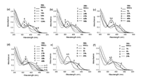
- the amount of reacted indium bromide was adjusted to 7 (Fig. 7a), 10 (Fig. 7b), 14 (Fig. 7c), 28 (Fig. 7d), 56 (Fig. 7e), 112 (Fig. 7f) equivalents compared to 386-InP MSCs. It was found that the higher the equivalence, the faster the synthesis rate at room temperature.
- the absorption band of the absorption spectrum of the finally synthesized F369-InP:Br nanoclusters was similar at 368 nm.
- the relative amount (Br/In) of bromide compared to indium of the F368-InP:Br nanoclusters was 0.53 when the amount of indium bromide reacted with 386-InP MSCs was 28 equivalents. .
- the amount of reacted indium bromide was adjusted to 7, 14, 28, 56, or 112 equivalents compared to 386-InP MSCs, there was no change in the absorption spectrum, but the relative amount of bromide compared to indium was changed from 0.18 to 0.68. Since the quantified amount of Br does not satisfy the total neutral charge of the nanoclusters, it is expected that the myristate ligand is simultaneously binding to the surface.
- InP nanoclusters InP MSCs, 386-InP MSCs
- the synthesis step consists of three steps: 386-InP MSCs synthesis, indium iodide precursor preparation, and precursor mixing.
- 386-InP MSCs had In-O bonding and In-P bonding values of 2.099 A and 2.528 A, respectively, and In-P bonding of 2.528 A. is the average bond length when having a polytwistane structure.
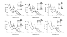
- the amount of indium iodide reacted with 386-InP MSCs to control the relative amount (I/In) of indium versus iodide of the F376-InP:I nanoclusters was 7 to 112 equivalents. Controlled and reacted at room temperature. 7 (Fig. 14a), 10 (Fig. 14b), 14 (Fig. 14c), 28 (Fig. 14d), 56 (Fig. 14e), 112 (Fig. 14f) equivalents of the reacted amount of indium iodide compared to 386-InP MSCs It was found that the higher the equivalent weight, the faster the synthesis rate at room temperature. The absorption band of the absorption spectrum of the finally synthesized F376-InP:I nanoclusters was similar at 376 nm.
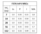
- the relative amount (I/In) of iodide to indium of the F376-InP:I nanocluster is 28 equivalents of indium iodide reacted with 386-InP MSCs was found to be 0.53.
- the amount of reacted indium iodide was adjusted to 7, 14, 28, 56, 112 equivalents compared to 386-InP MSCs, there was no change in the absorption spectrum, but the relative amount of iodide compared to indium was changed from 0.15 to 0.53. Since the quantified amount of I does not satisfy the total neutral charge of the nanoclusters, it is expected that the myristate ligand is simultaneously binding to the surface.
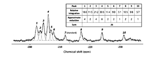
- the 31P NMR spectrum analysis result of the synthesized F376-InP:I nanocluster shows that the peaks of P constituting the cluster are integrated by integer multiples, resulting in a total of 26 Dog P was detected. This means that two types of clusters composed of 13 Ps are mixed.
Landscapes
- Chemical & Material Sciences (AREA)
- Engineering & Computer Science (AREA)
- Materials Engineering (AREA)
- Organic Chemistry (AREA)
- Nanotechnology (AREA)
- Physics & Mathematics (AREA)
- Condensed Matter Physics & Semiconductors (AREA)
- General Physics & Mathematics (AREA)
- Manufacturing & Machinery (AREA)
- Crystallography & Structural Chemistry (AREA)
- Luminescent Compositions (AREA)
- Inorganic Compounds Of Heavy Metals (AREA)
Abstract
본 발명은 III족 및 V족 원소를 포함하는 할로겐 원소 도핑 나노클러스터 및 이의 제조방법에 관한 것으로, 보다 구체적으로는, III족 원소 및 V족 원소를 포함하는 전구체 나노클러스터와 할로겐 전구 화합물과의 반응을 통해 제조된 할로겐 원소 도핑 나노클러스터에 관한 것이다.
Description
본 발명은 III족 및 V족 원소를 포함하는 할로겐 원소 도핑 나노클러스터 및 이의 제조방법에 관한 것으로, 보다 구체적으로는, III족 원소 및 V족 원소를 포함하는 전구체 나노클러스터와 할로겐 전구 화합물과의 반응을 통해 제조된 할로겐 원소 도핑 나노클러스터에 관한 것이다.
특정 개수의 금속 원자와 리간드로 구성되는 나노클러스터(nanocluster) 또는 거대원자(superatom)는 입자가 가지는 정전위상 전자(valence electron)가 새롭게 정의되는 거대원자 오비탈 이론을 따르며, 이를 하나의 거대한 원자로 보는 이론이다.
나노클러스터는 원자 하나 또는 나노입자 대비 안정적이며, 금속적인 성질보다 분자적인 성질이 강해 나노입자와는 전혀 다른 광학적 및 전기화학적 성질을 가진다. 특히, 나노클러스터는 금속 원자의 개수, 금속 원자의 종류 및 리간드 등에 따라 광학적, 전기적 및 촉매적 성질이 민감하게 달라짐에 따라, 매우 다양한 분야에서 나노클러스터에 관한 연구가 활발하게 진행 중이다.
반도체 나노입자는 발광효율이 높으며, 유기 염료 물질에 비해 광표백 현상에 대한 내구성이 뛰어난 장점을 가진다. 또한 나노입자 물질과 그 크기를 조절하여 가시광선에서 근적외선에 이르는 넓은 범위의 발광파장을 얻을 수 있으며, 특히 반도체 나노입자의 크기를 선택적으로 조절하여 좁은 색순도를 가지는 다양한 발광색을 구현할 수 있다. 반도체 나노입자의 우수한 광학적 특성을 응용하여 디스플레이, 태양전지, 생체 이미징과 같은 산업 및 의학 분야에 적용시키려는 연구가 활발히 이루어지고 있다. 상기와 같은 분야에 반도체 나노입자를 활용하기 위해서는 발광 스펙트럼에서 반치전폭(full-width at half-maximum, FWHM), 양자효율, 발광의 깜박임(blinking), 광안정성과 같은 광학적 특성이 중요하게 고려될 수 있다. 현재 이온결합성 물질인 카드뮴 칼코제나이드 기반의 II족-VI족 반도체 나노입자의 경우 좁은 발광의 반치전폭, 높은 양자효율과 같이 우수한 광학 특성을 가지지만 독성물질이 포함되어 있기에 해당 산업 전반 응용에 있어서 한계가 있다.
중금속 오염에 의한 생물 독성 위험을 극복하기 위하여 비중금속성 물질을 이용한 III족-V족 기반 반도체 나노입자의 개발이 진행되어 왔다. 예를 들어, III족-V족 기반의 InP 나노입자의 경우, 생체 독성이 낮고 발광 파장대가 가시광선 영역에 있기 때문에 카드뮴 칼코제나이드 나노입자를 대체하는 물질로 대두되고 있다. 그러나 III족-V족 기반의 InP 나노입자 성장 시, 결정 내의 결합 엔탈피와 표면 에너지 사이의 균형점을 찾아가는 과정에서 비평형상태의 여러 경로들을 통과하게 되어 불균질한 입자가 얻어지며, 형상의 조절의 한계를 보여 응용 면에서 많은 제약을 받고 있다.
최근에는 이러한 문제를 해결하기 위해 반응 중간체로 합성되는 나노클러스터 자체를 전구체로 이용하여 균일한 나노입자를 합성하는 연구가 주목받고 있다. 크기가 2 nm 이하인 III족-V족 반도체 나노클러스터를 나노입자 합성 전구체로 응용할 경우 일반적인 나노입자 합성 전구체인 분자 전구체를 이용하는 것보다 크기 균질도가 높은 나노입자를 합성할 수 있다.
또한 반도체 나노클러스터를 합성 전구체로 응용할 경우 나노막대, 나노와이어, 나노벨트 등의 다양한 모양을 가지는 반도체 나노구조체 개발이 가능하다. 다양한 모양의 반도체 나노구조체는 우수한 전기적, 광학적, 기계적, 열적 특성을 나타내기 때문에 화학 및 생물학적 센서, 전계효과 트렌지스터, 발광 다이오드 등의 디바이스 분야에서 응용될 수 있다. 일 예로 반도체 나노클러스터를 전구체로 활용하여 제조된 일차원 나노구조체의 경우 편광과 같은 독특한 광특성때문에 다양한 이점을 가진다.
그러나 현재까지 보고된 연구 결과들은 II족-VI족 카드뮴 기반 반도체 나노클러스터가 다수 보고되어 있고, III족-V족 반도체 나노클러스터는 극히 제한적인 종류만 보고되어 있는 실정이다. III족-V족 반도체 나노클러스터는 II족-VI족 반도체 나노클러스터에 비해 보다 우수한 응용성을 가지고 있는 점에서 보다 다양한 유도체를 제공함으로써 화학 및 생물학적 센서, 전계효과 트렌지스터, 발광 다이오드 등의 디바이스 분야에서 매우 유용한 소재로 활용될 수 있다.
따라서, 본 발명은 상기한 바와 같은 종래 기술의 문제점을 해결하기 위하여 안출된 것으로, 본 발명의 목적은 III족 및 V족 원소를 포함하는 할로겐 원소 도핑 나노클러스터 및 이의 제조방법을 제공함에 있다. 보다 구체적으로는, III족 원소 및 V족 원소를 포함하는 전구체 나노클러스터와 할로겐 전구 화합물과의 반응을 통해 할로겐 원소 도핑 나노클러스터을 제공하고, 다양한 할로겐 도핑 함량을 가지는 나노클러스터 및 이의 제조방법을 제공함에 있다.
상기 목적을 달성하기 위한 본 발명은, III족 원소 및 V족 원소를 포함하고 하기 화학식 1로 표시되는 할로겐 원소 도핑 나노클러스터를 제공한다.
[화학식 1]
M1
xM2
yLzXk
(상기 화학식 1에서 x는 20 내지 60의 정수, y는 4 내지 36의 정수, z는 10 내지 120의 정수, k는 2 내지 50의 정수, M1은 III족 원소, M2는 V족 원소, X는 할로겐 원자, L은 알킬카르복실, 알케닐카르복실, 알킬카보닐, 알케닐카보닐, 알킬옥시, 알케닐옥시 또는 아릴옥시의 리간드이다.)
일 측면에 따르면, 상기 할로겐 원소 도핑 나노클러스터는 368nm에서 최대 흡수파장을 가지며, X는 Br일 수 있다.
일 측면에 따르면, 상기 할로겐 원소 도핑 나노클러스터는 376nm에서 최대 흡수파장을 가지며, X는 I일 수 있다.
일 측면에 따르면, 상기 할로겐 원소 도핑 나노클러스터는 386nm에서 최대 흡수파장을 가지는 전구체 나노클러스터에서 유래된 것일 수 있다.
일 측면에 따르면, 상기 할로겐 원소 도핑 나노 클러스터에서 M1은 In이며, M2는 P일 수 있다.
일 측면에 따르면, 상기 전구체 나노클러스터는 In37P20(O2CR)51일 수 있다. (R은 (C1-C20)알킬 또는 (C2-C2-)알케닐을 의미한다)
일 측면에 따르면, 상기 할로겐 원소 도핑 나노 클러스터는 polytwistane 구조를 가질 수 있다.
일 측면에 따르면, 상기 할로겐 원소 도핑 나노클러스터는 1 내지 3 nm의 직경을 가질 수 있다.
일 측면에 따르면, 상기 할로겐 원소 도핑 나노클러스터로부터 할로겐 원소 도핑 나노입자를 제조할 수 있다.
또한 본 발명은 할로겐 원소 도핑 나노클러스터의 제조방법을 제공하며, III족 원소 및 V족 원소를 포함하는 전구체 나노클러스터를 제조하는 제1단계; M1X3 용액에 상기 전구체 나노클러스터를 혼합하여 반응용액을 제조하는 제2단계; 및 상기 반응용액을 가열하여 반응하는 제3단계;를 포함한다.
일 측면에 따르면, 상기 III족 원소 및 V족 원소를 포함하는 전구체 나노클러스터를 제조하는 단계는, M1(C2-C4 알킬카르복실)3, C6-C16 지방산 및 포스핀 전구체 화합물을 혼합 및 반응하는 것일 수 있다.
일 측면에 따르면, 상기 제3단계에서 가열온도는 20 내지 170℃일 수 있다.
일 측면에 따르면, 상기 제2단계에서, 전구체 나노클러스터 분자에 대해 M1X3 분자가 과량의 당량으로 투입될 수 있다.
본 발명에 의하면, III족 및 V족 원소를 포함하는 할로겐 원소 도핑 나노클러스터 및 이의 제조방법을 제공할 수 있다. 보다 구체적으로는, 본 발명에 따른 III족 및 V족 원소를 포함하는 할로겐 원소 도핑 나노클러스터는 2 nm 이하에 속하여, 분자의 구조가 열역학적 국소점에 해당하여 작은 크기임에도 불구하고 특이적으로 안정한 구조로 존재하는 매직 크기 클러스터(magic-size cluster, MSC)의 구조이다.
또한 본 발명에 의하면, III족 원소 및 V족 원소를 포함하는 전구체 나노클러스터와 할로겐 전구 화합물의 반응조건을 조절함으로써 다양한 할로겐 도핑 함량을 가지며, III족 원소 및 V족 원소를 포함하는 전구체 나노클러스터의 최대 흡수파장과 상이한 최대 흡수파장을 가지는 나노클러스터를 제공할 수 있다.
본 발명에 따른 할로겐 원소 도핑 나노클러스터를 나노입자 합성 전구체로 응용시, 일반적인 나노입자 합성 전구체인 분자 전구체를 이용하는 것보다 나노입자의 크기 균질도 및 물리화학적 특성이 균일한 나노입자가 높은 재현성으로 합성될 수 있다. 특히 나노입자의 형상을 자유롭게 조절할 수 있는 전구체로서 바람직하게 활용될 수 있다. 예시적으로, 할로겐 원소 도핑 나노클러스터를 전구체로 사용하여 비등방성 나노입자를 합성함으로써, 비등방성 나노입자가 가지는 우수한 전기적, 광학적, 기계적 및 열적 특성에 의해 화학 및 생물학적 센서, 전계효과 트렌지스터, 발광 다이오드 등의 디바이스 분야에서 바람직하게 응용될 수 있으며, 할로겐 원소가 도핑됨에 따라 기존의 III족 및 V족 원소의 반도체 나노입자 대비 차별화된 물리화학적 특성을 구현할 수 있는 잠재성을 가진다.
도 1은 F368-InP:Br 나노클러스터, F376-InP:I 나노클러스터의 흡수 스펙트럼이다.
도 2는 F368-InP:Br 나노클러스터를 386-InP MSCs와 28 당량의 InBr3를 이용하여 상온에서 135℃로 승온하여 화학 변환 합성한 성장 과정의 흡수 스펙트럼이다.
도 3는 386-InP MSCs, F368-InP:Br 나노클러스터의 TEM 이미지이다.
도 4은 386-InP MSCs, F368-InP:Br 나노클러스터의 XRD 패턴이다.
도 5은 386-InP MSCs, F368-InP:Br 나노클러스터의 EXAFS 스펙트럼이다.
도 6은 386-InP MSCs, F368-InP:Br 나노클러스터의 In 3d3/2 XPS 스펙트럼이다.
도 7는 386-InP MSCs와 반응하는 InBr3의 당량을 변화 시키며 상온에서 F368-InP:Br 나노클러스터를 화학 변환 합성한 결과의 흡수 스펙트럼이다. 386-InP MSCs 대비 각각 (a) 7, (b) 10, (c) 14, (d) 28, (e) 56, (f) 112 당량의 InBr3이 반응한 것을 의미한다.
도 8는 386-InP MSCs와 반응하는 InBr3의 당량을 변화 시키며 F368-InP:Br 나노클러스터를 화학 변환 합성 시 원소비 분석 결과이다. In, P, Br의 원소 분석은 EDX 측정, MA의 정량값은 전체 나노클러스터의 전하가 0임을 가정하여 계산하였다.
도 9는 F376-InP:I 나노클러스터를 386-InP MSCs와 28 당량의 InI3를 이용하여 상온에서 150℃로 승온하여 화학 변환 합성한 성장 과정의 흡수 스펙트럼이다.
도 10는 386-InP MSCs, F376-InP:I 나노클러스터의 TEM 이미지이다.
도 11은 386-InP MSCs, F376-InP:I 나노클러스터의 XRD 패턴이다.
도 12은 386-InP MSCs, F376-InP:I 나노클러스터의 EXAFS 스펙트럼이다.
도 13은 386-InP MSCs, F376-InP:I 나노클러스터의 In 3d3/2 XPS 스펙트럼이다.
도 14는 386-InP MSCs와 반응하는 InI3의 당량을 변화 시키며 상온에서 F376-InP:I 나노클러스터를 화학 변환 합성한 결과의 흡수 스펙트럼이다. 386-InP MSCs 대비 각각 (a) 7, (b) 10, (c) 14, (d) 28, (e) 56, (f) 112 당량의 InI3이 반응한 것을 의미한다.
도 15는 386-InP MSCs와 반응하는 InI3의 당량을 변화 시키며 F376-InP:I 나노클러스터를 화학 변환 합성 시 원소비 분석 결과이다. In, P, I의 원소 분석은 EDX 측정, MA의 정량값은 전체 나노클러스터의 전하가 0임을 가정하여 계산하였다.
도 16은 386-InP MSCs와 반응하는 InI3가 7 당량일 때, 합성되는 F376-InP:I 나노클러스터의 31P NMR 스펙트럼이다.
이하 첨부한 도면들을 참조하여 본 발명에 III족 및 V족 원소를 포함하는 할로겐 원소 도핑 나노클러스터 및 이의 제조방법을 상세히 설명한다. 다음에 소개되는 도면들은 당업자에게 본 발명의 사상이 충분히 전달될 수 있도록 하기 위해 예로서 제공되는 것이다. 따라서, 본 발명은 이하 제시되는 도면들에 한정되지 않고 다른 형태로 구체화될 수도 있으며, 이하 제시되는 도면들은 본 발명의 사상을 명확히 하기 위해 과장되어 도시될 수 있다. 이때, 사용되는 기술 용어 및 과학 용어에 있어서 다른 정의가 없다면, 이 발명이 속하는 기술 분야에서 통상의 지식을 가진 자가 통상적으로 이해하고 있는 의미를 가지며, 하기의 설명 및 첨부 도면에서 본 발명의 요지를 불필요하게 흐릴 수 있는 공지 기능 및 구성에 대한 설명은 생략한다.
또한 명세서 및 첨부된 청구범위에서 사용되는 단수 형태는 문맥에서 특별한 지시가 없는 한 복수 형태도 포함하는 것으로 의도할 수 있다.
본 명세서 및 첨부된 청구범위에서 제1, 제2 등의 용어는 한정적인 의미가 아니라 하나의 구성 요소를 다른 구성 요소와 구별하는 목적으로 사용된다.
본 명세서 및 첨부된 청구범위에서 ‘포함하다’ 또는 ‘가지다’ 등의 용어는 명세서상에 기재된 특징, 또는 구성요소가 존재함을 의미하는 것이고, 특별히 한정하지 않는 한, 하나 이상의 다른 특징들 또는 구성요소가 부가될 가능성을 미리 배제하는 것은 아니다.
본 명세서 및 첨부된 청구범위에서 최대 흡수파장의 수치는 최대 흡수파장 수치의 ±2%의 오차범위를 포함하는 것일 수 있다.
본 명세서 및 첨부된 청구범위에서 나노클러스터(nanocluster)는 수퍼아톰(superatom) 또는 매직 크기 클러스터(magic-size cluster, MSC)와 동일한 의미로 사용된다.
반도체 나노입자의 구조나 형상을 정확하게 조절하기 위한 합성방법은 지속적으로 연구되어져 왔지만, 주로 구형의 입자나 결정면을 가지는 나노결정형 입자 등이 합성되었다. 나노로드, 나노판상형 입자와 같은 종횡비가 큰 반도체 나노입자 등이 개발된 바 있지만, 우수한 광학적, 전기적 특성을 가지는 비등방성 나노입자를 높은 재현성으로 합성한 연구는 보고되지 않았다. 특히 II족-VI족 반도체 나노입자의 구조나 형상을 조절하기 위한 연구는 다수 수행된 반면, InP, GaP, InAs 등의 III족-V족 반도체 나노입자의 비등방성을 구현하기 위한 연구는 일부만 보고되었다. 이는 III족-V족 반도체는 II족-VI족 반도체에 비해 공유결합적 성질이 보다 강하기 때문에 서로 다른 결정면 사이의 대비가 보다 완만하여 대체로 구형의 입자나 결정면을 가지는 나노결정형 입자의 합성이 더 선호되기 때문이다.
상기와 같은 문제를 해결하기 위해 나노클러스터를 나노입자 합성 전구체로 이용하여 균일한 나노입자가 합성될 수 있음을 발견하고 이에 대한 연구를 심화하였으며, 특정 반응물 및 반응조건에서 할로겐 원소가 나노클러스터에 다양한 함량으로 도핑될 수 있음을 확인하여, 본 발명을 완성하기에 이르렀다.
본 발명에 따른 III족 및 V족 원소를 포함하는 할로겐 원소 도핑 나노클러스터는 나노입자의 합성 전구체로 바람직하게 사용될 수 있으며, 나노입자의 크기 균질도 및 물리화학적 특성이 균일한 나노입자가 높은 재현성으로 합성될 수 있다. 특히 할로겐 원소 도핑 나노클러스터를 전구체로 사용하여 비등방성 나노입자를 합성함으로써, 비등방성 나노입자가 가지는 우수한 전기적, 광학적, 기계적 및 열적 특성을 가질 수 있을 뿐만 아니라, 할로겐 원소가 도핑됨에 따라 기존의 III족 및 V족 원소의 반도체 나노입자 대비 차별화된 물리화학적 특성을 구현할 수 있다.
전술한 바와 같은 작용효과를 구현하기 위해, 본 발명에 따른 할로겐 원소 도핑 나노클러스터는 화학식 1을 만족하는 나노클러스터임을 특징으로 한다.
[화학식 1]
M1
xM2
yLzXk
상기 화학식 1에서 x는 x는 20 내지 60의 정수, y는 4 내지 36의 정수, z는 10 내지 120의 정수, k는 2 내지 50의 정수, M1은 III족 원소, M2는 V족 원소, X는 할로겐 원자, L은 알킬카르복실, 알케닐카르복실, 알킬카보닐, 알케닐카보닐, 알킬옥시, 알케닐옥시 또는 아릴옥시의 리간드이다.
구체적으로, L은 C2-C20 알킬카르복실, C2-C20 알케닐카르복실, C2-C20 알킬카보닐, C2-C20 알케닐카보닐, C1-C20 알킬옥시, C1-C20 알케닐옥시 또는 C6-C20 아릴옥시의 리간드일 수 있으며, 보다 구체적으로, L은 C10-C20 알킬카르복실, C10-C20 알케닐카르복실, C10-C20 알킬카보닐, C10-C20 알케닐카보닐, C10-C20 알킬옥시, C10-C20 알케닐옥시 또는 C6-C12 아릴옥시의 리간드일 수 있다.
비한정적으로 나노클러스터에 포함되는 III족 원소 및 V족 원소의 총 합은 20 내지 160일 수 있고, 구체적으로 60 내지 140일 수 있다.
일 양태에 따르면, M1은 III족 원소로서 Al, Ga, In 또는 TI일 수 있으며, M2는 V족 원소로서 P, As, Sb 또는 Bi일 수 있다. 예시적인 조합으로는 GaP, GaAs, GaSb, InP, InAs 또는 InSb 등일 수 있으나 이에 제한받지 않는다. 바람직한 일 양태에 따르면 M1과 M2가 조합된 반도체 화합물은 InP일 수 있다.
일 양태에 따르면, 할로겐 원소 X는 Br일 수 있으며, 구체적으로 Br이 InP 나노클러스터에 도핑된 것일 수 있다. 구체적인 일 양태에 따르면, 상기 Br이 도핑된 나노클러스터는 368nm에서 최대 흡수파장을 가질 수 있다. 구체적인 예를 들어, 386nm에서 최대 흡수파장을 가지는 386-InP 나노클러스터는 In37P20(O2CR)51 (R=C13 알킬)로 표시될 수 있으며, 상기 386-InP 나노클러스터에 Br이 도핑됨에 따라 단파장 방향으로 최대 흡수파장이 이동되어 368nm에서 최대 흡수파장을 가질 수 있다.
도핑되는 Br의 양은 할로겐 전구 화합물의 당량을 조절함으로써 용이하게 조절될 수 있다. 예를 들어, 368nm에서 최대 흡수파장을 가지는 Br 도핑 나노클러스터인 F368-InP:Br의 경우, 인듐 1몰에 대해, 브롬 원소(Br)는 0.1 내지 0.8몰의 함량으로 도핑될 수 있으며, 구체적으로 0.15 내지 0.7몰의 함량, 보다 구체적으로 0.18 내지 0.68몰의 함량으로 도핑될 수 있다. 한편 브롬이 도핑됨에 따라, 인의 함량은 0.25 내지 0.5몰의 함량으로 포함될 수 있으며, 구체적으로 0.28 내지 0.47몰, 보다 구체적으로 0.31 내지 0.44몰의 함량으로 포함될 수 있다.
일 양태에 따르면, 할로겐 원소 X는 I일 수 있으며, 구체적으로 I가 InP 나노클러스터에 도핑된 것일 수 있다. 구체적인 일 양태에 따르면, 상기 I가 도핑된 나노클러스터는 376nm에서 최대 흡수파장을 가질 수 있다. 구체적인 예를 들어, 386nm에서 최대 흡수파장을 가지는 386-InP 나노클러스터는 In37P20(O2CR)51 (R=C13 알킬)로 표시될 수 있으며, 상기 386-InP 나노클러스터에 I가 도핑됨에 따라 단파장 방향으로 최대 흡수파장이 이동되어 376nm에서 최대 흡수파장을 가질 수 있다.
도핑되는 I의 양은 할로겐 전구 화합물의 당량을 조절함으로써 용이하게 조절될 수 있다. 예를 들어, 376nm에서 최대 흡수파장을 가지는 I 도핑 나노클러스터인 F376-InP:I의 경우, 인듐 1몰에 대해, 요오드 원소(I)는 0.1 내지 0.6몰의 함량으로 도핑될 수 있으며, 구체적으로 0.12 내지 0.55몰의 함량, 보다 구체적으로 0.15 내지 0.53몰의 함량으로 도핑될 수 있다. 한편 요오드가 도핑됨에 따라, 인의 함량은 0.25 내지 0.4몰의 함량으로 포함될 수 있으며, 구체적으로 0.28 내지 0.38몰, 보다 구체적으로 0.31 내지 0.35몰의 함량으로 포함될 수 있다.
일 양태에 따르면, F376-InP:I 및 F368-InP:Br는 polytwistane 구조를 가지는 것일 수 있다.
전술한 바와 같은 할로겐 원소 도핑 나노클러스터는 1 내지 3 nm의 평균 입경을 가질 수 있으며, 구체적으로 1 내지 2 nm의 입경을 가질 수 있으나 이에 제한받지 않는다.
또한 본 발명은 하기 화학식 1을 만족하는 할로겐 원소 도핑 나노클러스터의 제조방법을 제공하며, 상기 제조방법은 III족 원소 및 V족 원소를 포함하는 전구체 나노클러스터를 제조하는 제1단계; M1X3 용액에 상기 전구체 나노클러스터를 혼합하여 반응용액을 제조하는 제2단계; 및 상기 반응용액을 가열하여 반응하는 제3단계를 포함한다.
[화학식 1]
M1
xM2
yLzXk
상기 화학식 1에서 x는 x는 20 내지 60의 정수, y는 4 내지 36의 정수, z는 10 내지 120의 정수, k는 2 내지 50의 정수, M1은 III족 원소, M2는 V족 원소, X는 할로겐 원자, L은 알킬카르복실, 알케닐카르복실, 알킬카보닐, 알케닐카보닐, 알킬옥시, 알케닐옥시 또는 아릴옥시의 리간드이다.
상기 III족 원소 및 V족 원소를 포함하는 전구체 나노클러스터를 제조하는 제1단계는, M1(C2-C4 알킬카르복실)3, C6-C16 지방산 및 포스핀 전구체 화합물을 혼합 및 반응하여 얻어지는 것일 수 있다. 이때 포스핀 전구체 화합물은 트리스(트리알킬실릴)포스핀 화합물일 수 있으며, 이때 알킬기는 C1-C4 알킬기일 수 있다. 구체적인 예로 트리스(트리메틸실릴)포스핀, 트리스(트리에틸실릴)포스핀, 트리스(트리프로필실릴)포스핀일 수 있다.
M1(C2-C4 알킬카르복실)3과 포스핀 전구체 화합물의 몰비는 1:0.1 내지 1:10일 수 있으며, 구체적으로 1:0.1 내지 1:2, 보다 구체적으로 1:0.2 내지 0.8일 수 있다. 또한 M1(C2-C4 알킬카르복실)3과 C6-C16 지방산의 몰비는 1:1 내지 1:10일 수 있으며, 구체적으로 1:2 내지 1:5일 수 있다.
반응용매로는 지방족 용매일 수 있으며, C10-C30의 지방족 용매일 수 있다. 구체적으로 C10-C30 알켄계 용매, 보다 구체적으로 C12-C20 알켄계 용매일 수 있다.
M1(C2-C4 알킬카르복실)3은 구체적으로 In(Ac)3일 수 있다. C6-C16 지방산은 장쇄 지방산으로서 포화 지방산 또는 불포화 지방산일 수 있으며, 구체적으로 미리스트산일 수 있다.
제1단계의 반응온도는 70 내지 170℃의 온도범위일 수 있으며, 비활성 기체 분위기에서 수행될 수 있다.
제1단계에서 얻어진 전구체 나노클러스터는 하기 화학식 2로 표시될 수 있다.
[화학식 2]
M1
aM2
bLc
상기 화학식 2에서 a는 20 내지 60의 정수, b는 10 내지 30의 정수, c는 10 내지 100의 정수, M1은 III족 원소, M2는 V족 원소, L은 알킬카르복실, 알케닐카르복실, 알킬카보닐, 알케닐카보닐, 알킬옥시, 알케닐옥시 또는 아릴옥시의 리간드이다.
보다 구체적으로, L은 C2-C20 알킬카르복실, C2-C20 알케닐카르복실, C2-C20 알킬카보닐, C2-C20 알케닐카보닐, C1-C20 알킬옥시, C1-C20 알케닐옥시 또는 C6-C20 아릴옥시의 리간드일 수 있으며, 보다 구체적으로, L은 C10-C20 알킬카르복실, C10-C20 알케닐카르복실, C10-C20 알킬카보닐, C10-C20 알케닐카보닐, C10-C20 알킬옥시, C10-C20 알케닐옥시 또는 C6-C12 아릴옥시의 리간드일 수 있다.
비한정적이고 구체적인 일 예시로, 전구체 나노클러스터는 In37P20(O2CR)51 (R=C13 알킬)일 수 있고, 상기 나노클러스터를 합성하기 위한 반응물로는, In(Ac)3, 미리스트산 및 트리스(트리메틸실릴)포스핀이 사용될 수 있다.
전구체 나노클러스터가 합성된 후, 제2단계에서 M1X3 용액에 상기 전구체 나노클러스터를 혼합하여 반응용액을 제조한다. 상기 제2단계에서, 전구체 나노클러스터 분자에 대해 M1X3 분자가 과량의 당량으로 투입될 수 있으며, 구체적으로, 전구체 나노클러스터 분자 1몰에 M1X3 분자가 7 내지 560 몰이 투입되어 혼합될 수 있다.
제3단계에서는 상기 반응용액을 가열함으로써 할로겐 원소가 도핑된 나노클러스터가 제조될 수 있다.
제3단계에서, 전구체 나노클러스터와 M1X3의 반응온도는 20 내지 170℃일 수 있으며, 구체적으로 80 내지 내지 170℃일 수 있고, 비활성 기체 분위기에서 수행될 수 있다. 이때 도핑하고자하는 할로겐 원소의 종류, 함량에 따라 반응온도는 다르게 설정될 수 있다. 예를 들어, Br을 도핑할 경우 120 내지 150℃의 온도범위에서 교반 가열하여 반응을 수행할 수 있다. 또한 I를 도핑할 경우 135 내지 165℃의 온도범위에서 교반 가열하여 반응을 수행할 수 있다.
전술한 바와 같이 본 발명에 따라 합성된 할로겐 원소 도핑 나노클러스터는 III족 원소 및 V족 원소를 포함하는 나노입자의 합성 전구체로서, 바람직하게 할로겐 원소가 도핑된 나노입자의 합성을 위해 바람직하게 활용될 수 있다.
이하 본 발명을 실시예에 의해 구체적으로 설명한다. 아래에서 설명하는 실시예는 발명의 이해를 돕기 위한 것일 뿐, 본 발명이 실시예에 한정되지 않는다.
[실시예 1] F368-InP:Br 나노클러스터의 합성
F368-InP:Br 나노클러스터의 화학 변환 합성의 경우 386 nm 파장에서 밴드흡수를 나타내는 InP 나노클러스터 (InP MSCs, 386-InP MSCs)를 전구체로 이용하였다. 합성 단계는 386-InP MSCs 합성, 인듐 브로마이드 전구체 준비, 전구체 혼합의 세가지 단계로 이루어진다.
(1) 386-InP MSCs 합성: 0.8 mmol 인듐 아세테이트, 2.9 mmol 미리스트산(MA), 20 mL 1-옥타데센 용매를 혼합 후 110℃ 온도에서 0.4 mmol 트리스(트리메틸실릴)포스핀 전구체를 주입하여 질소 환경에서 2시간 반응 후 종료한다.
(2) 인듐 브로마이드 전구체 준비: 10 mL 1-옥타데센 용매에 0.25 mmol 인듐 브로마이드 전구체를 분산 후 110℃ 온도에서 반응 용액을 진공 상태에서 1시간 교반 가열하고 25℃ 온도로 낮춘다.
(3) 386-InP MSCs와 인듐 브로마이드(InBr3)의 혼합: 합성한 386-InP MSCs 용액 20 mL를 인듐 브로마이드 용액과 상온에서 혼합 후 135℃로 승온, 질소 환경에서 반응시킨다.
386-InP MSCs와 28당량의 인듐 브로마이드를 상온에서 혼합 후 135℃까지 승온시키면 F368-InP:Br 나노클러스터가 화학 변환을 통해 합성된다. 도 2를 참조하면, 흡수밴드가 연속적으로 변하지 않고 비연속적으로 양자화된 변환 패턴을 보이는 것을 알 수 있다.
[실시예 2] F368-InP:Br 나노클러스터의 크기 특성 규명
F368-InP:Br 나노클러스터 합성 시 이용한 386-InP MSCs와 개발한 F368-InP:Br 나노클러스터의 크기 특성 관찰 결과, 도 3을 참조하면, TEM 이미지에서 386-InP MSCs, F368-InP:Br 나노클러스터는 평균 1.7 nm 직경으로 확인되었다. F368-InP:Br 나노클러스터의 경우 386-InP MSCs보다 흡수밴드가 단파장이므로 크기가 더 작을 것으로 추정되지만 TEM으로 크기 구별이 어려운 것으로 보인다.
[실시예 3] F368-InP:Br 나노클러스터의 구조 특성 규명
F368-InP:Br 나노클러스터 합성 시 이용한 386-InP MSCs와 합성된 F368-InP:Br 나노클러스터의 구조 특성 분석 결과, 도 4를 참조하면, 386-InP MSCs, F368-InP:Br 나노클러스터의 XRD 패턴이 유사하여 두 종 모두 알려진 polytwistane 구조로 확인되었다.
도 5를 참조하면, EXAFS (Extended X-ray Absorption Fine Structure) 분석 결과, 386-InP MSCs는 In-O 결합, In-P 결합이 각각 2.099 A, 2.528 A 값으로 측정되었으며 2.528 A의 In-P 결합은 polytwistane 구조를 가질 때의 평균 결합길이이다. 또한 합성된 F368-InP:Br 나노클러스터의 EXAFS 스펙트럼 분석 결과 In-O 결합, In-P 결합이 각각 2.142 A, 2.512 A 값으로 측정되었으며 polytwistane 구조가 가질 수 있는 In-P 결합 길이로 나타나 F368-InP:Br 나노클러스터는 polytwistane 구조를 가짐을 확인하였다.
[실시예 4] F368-InP:Br 나노클러스터의 표면 특성 규명
도 6을 참조하면, F368-InP:Br 나노클러스터 합성 시 이용한 386-InP MSCs와 F368-InP:Br 나노클러스터의 표면 리간드 분석 결과 F368-InP:Br 나노클러스터의 XPS 스펙트럼에서 In 3d5/2 피크의 binding energy 값이 445.3 eV로 386-InP MSCs의 binding energy 값인 444.8 eV 보다 크며 In 표면에 Br이 결합되어 있는 것으로 확인되었다.
[실시예 5] F368-InP:Br 나노클러스터 합성 시 Br 도핑 함량 조절
F368-InP:Br 나노클러스터의 인듐 대비 브로마이드의 상대양(Br/In)을 조절하기 위해 386-InP MSCs와 반응시키는 인듐 브로마이드의 양을 7 내지 112 당량으로 조절하여 도 7과 같이 상온에서 반응시켰다. 반응시키는 인듐 브로마이드의 양을 386-InP MSCs 대비 7 (도7a), 10 (도7b), 14 (도7c), 28 (도7d), 56 (도7e), 112 (도7f) 당량으로 조절 시 높은 당량 일수록 상온에서 합성 속도가 빠른 것으로 나타났다. 최종 합성된 F369-InP:Br 나노클러스터의 흡수 스펙트럼의 흡수밴드는 368 nm로 유사하였다.
[실시예 6] F368-InP:Br 나노클러스터의 조성 특성 규명
도 8을 참조하면, EDX 원소 분석 결과 F368-InP:Br 나노클러스터의 인듐 대비 브로마이드의 상대양(Br/In)이 386-InP MSCs와 반응시키는 인듐 브로마이드의 양이 28 당량일 때 0.53으로 확인되었다. 반응시키는 인듐 브로마이드의 양을 386-InP MSCs 대비 7, 14, 28, 56, 112 당량으로 조절 시 흡수 스펙트럼의 변화는 없으나 인듐 대비 브로마이드의 상대양이 0.18~0.68까지 변화되었다. 정량된 Br 양으로 나노클러스터의 전체 중성 전하를 만족시키지 못하므로 미리스테이트 리간드가 동시에 표면에 결합하고 있을 것으로 예상된다.
[실시예 7] F376-InP:I 나노클러스터의 합성
F376-InP:I 나노클러스터의 화학 변환 합성의 경우 386 nm 파장에서 밴드흡수를 나타내는 InP 나노클러스터(InP MSCs, 386-InP MSCs)를 전구체로 이용하였다. 합성 단계는 386-InP MSCs 합성, 인듐 아이오다이드 전구체 준비, 전구체 혼합의 세가지 단계로 이루어진다.
(1) 386-InP MSCs 합성: 0.8 mmol 인듐 아세테이트, 2.9 mmol 미리스트산, 20 mL 1-옥타데센 용매를 혼합 후 110℃ 온도에서 0.4 mmol 트리스(트라이메틸실릴)포스핀 전구체를 주입하여 질소 환경에서 2시간 반응 후 종료한다.
(2) 인듐 아이오다이드 전구체 준비: 10 mL 1-옥타데센 용매에 0.25 mmol 인듐 아이오다이드 전구체를 분산 후 110℃ 온도에서 반응 용액을 진공 상태에서 1시간 교반 가열하고 25 ℃ 온도로 낮춘다.
(3) 386-InP MSCs와 인듐 아이오다이드(InI3)의 혼합: 합성한 386-InP MSCs 용액 20 mL를 인듐 아이오다이드 용액과 상온에서 혼합 후 150℃로 승온, 질소 환경에서 반응시킨다.
386-InP MSCs와 28당량의 인듐 아이오다이드를 상온에서 혼합 후 150℃까지 승온시키면 F376-InP:I 나노클러스터가 화학 변환을 통해 합성된다. 도 9를 참조하면, 흡수밴드가 연속적으로 변하지 않고 비연속적으로 양자화된 변환 패턴을 보이는 것을 알 수 있다.
[실시예 8] F376-InP:I 나노클러스터의 크기 특성 규명
도 10을 참조하면, F376-InP:I 나노클러스터 합성 시 이용한 386-InP MSCs와 개발한 F376-InP:I 나노클러스터의 크기 특성 관찰 결과, TEM 이미지에서 386-InP MSCs, F376-InP:I 나노클러스터는 평균 1.7 nm 직경으로 확인되었다. F376-InP:I 나노클러스터의 경우 386-InP MSCs보다 흡수밴드가 단파장이므로 크기가 더 작을 것으로 추정되나 TEM으로 크기 구별이 어려운 것으로 보인다.
[실시예 9] F376-InP:I 나노클러스터의 구조 특성 규명
F376-InP:I 나노클러스터 합성 시 이용한 386-InP MSCs와 합성된 F376-InP:I 나노클러스터의 구조 특성 분석 결과, 도 11을 참조하면, 386-InP MSCs, F376-InP:I 나노클러스터의 XRD 패턴이 유사하여 두 종 모두 알려진 polytwistane 구조로 확인되었다.
도 12를 참조하면, EXAFS (Extended X-ray Absorption Fine Structure) 분석 결과 386-InP MSCs는 In-O 결합, In-P 결합이 각각 2.099 A, 2.528 A 값으로 측정되었으며 2.528 A의 In-P 결합은 polytwistane 구조를 가질 때의 평균 결합길이이다. 또한 합성된 F376-InP:I 나노클러스터의 EXAFS 스펙트럼 분석 결과 In-O 결합, In-P 결합이 각각 2.149 A, 2.506 A 값으로 측정되었으며 polytwistane 구조가 가질 수 있는 In-P 결합 길이로 나타나 F376-InP:I 나노클러스터는 polytwistane 구조를 가짐을 확인하였다.
[실시예 10] F376-InP:I 나노클러스터의 표면 특성 규명
도 13을 참조하면, F376-InP:I 나노클러스터 합성 시 이용한 386-InP MSCs와 F376-InP:I 나노클러스터의 표면 리간드 분석 결과 F376-InP:I 나노클러스터의 XPS 스펙트럼에서 In 3d5/2 피크의 binding energy 값이 444.8 eV로 386-InP MSCs의 binding energy 값인 444.8 eV 과 유사한 것으로 나타났다.
[실시예 11] F376-InP:I 나노클러스터 합성 시 I 도핑 함량 조절
도 14를 참조하면, F376-InP:I 나노클러스터의 인듐 대비 아이오다이드의 상대양(I/In)을 조절하기 위해 386-InP MSCs와 반응시키는 인듐 아이오다이드의 양을 7 내지 112 당량으로 조절하여 상온에서 반응시켰다. 반응시키는 인듐 아이오다이드의 양을 386-InP MSCs 대비 7 (도14a), 10 (도14b), 14 (도14c), 28 (도14d), 56 (도14e), 112 (도14f) 당량으로 조절 시 높은 당량 일수록 상온에서 합성 속도가 빠른 것으로 나타났다. 최종 합성된 F376-InP:I 나노클러스터의 흡수 스펙트럼의 흡수밴드는 376 nm로 유사하였다.
[실시예 12] F376-InP:I 나노클러스터의 조성 특성 규명
도 15를 참조하면, EDX 원소 분석 결과 F376-InP:I 나노클러스터의 인듐 대비 아이오다이드의 상대양(I/In)이 386-InP MSCs와 반응시키는 인듐 아이오다이드의 양이 28 당량일 때 0.53으로 확인되었다. 반응시키는 인듐 아이오다이드의 양을 386-InP MSCs 대비 7, 14, 28, 56, 112 당량으로 조절 시 흡수 스펙트럼의 변화는 없으나 인듐 대비 아이오다이드의 상대양이 0.15~0.53까지 변화되었다. 정량된 I 양으로 나노클러스터의 전체 중성 전하를 만족시키지 못하므로 미리스테이트 리간드가 동시에 표면에 결합하고 있을 것으로 예상된다.
도 16을 참조하면, 386-InP MSCs와 반응하는 InI3가 7 당량일 때, 합성되는 F376-InP:I 나노클러스터의 31P NMR 스펙트럼 분석 결과 클러스터를 구성하는 P의 피크가 정수배로 적분되어 총 26개의 P가 검출되었다. 이는 13개의 P로 구성된 2 종류의 클러스터가 혼합되어 있는 것을 의미한다.
Claims (13)
- III족 원소 및 V족 원소를 포함하고 하기 화학식 1을 만족하는, 할로겐 원소 도핑 나노클러스터.[화학식 1]M1 xM2 yLzXk(상기 화학식 1에서 x는 20 내지 60의 정수, y는 4 내지 36의 정수, z는 10 내지 120의 정수, k는 2 내지 50의 정수, M1은 III족 원소, M2는 V족 원소, X는 할로겐 원자, L은 알킬카르복실, 알케닐카르복실, 알킬카보닐, 알케닐카보닐, 알킬옥시, 알케닐옥시 또는 아릴옥시의 리간드이다.)
- 제1항에 있어서,상기 할로겐 원소 도핑 나노클러스터는 368nm에서 최대 흡수파장을 가지며, X는 Br인, 할로겐 원소 도핑 나노클러스터.
- 제1항에 있어서,상기 할로겐 원소 도핑 나노클러스터는 376nm에서 최대 흡수파장을 가지며, X는 I인, 할로겐 원소 도핑 나노클러스터.
- 제1항에 있어서,상기 할로겐 원소 도핑 나노클러스터는 386nm에서 최대 흡수파장을 가지는 전구체 나노클러스터에서 유래된 것인, 할로겐 원소 도핑 나노클러스터.
- 제1항에 있어서,M1은 In이며, M2는 P인, 할로겐 원소 도핑 나노클러스터.
- 제4항에 있어서,상기 전구체 나노클러스터는 In37P20(O2CR)51인, 할로겐 원소 도핑 나노클러스터.(R은 C1-C20의 알킬 또는 C2-C20의 알케닐을 의미한다.)
- 제1항 내지 제6항 중 어느 한 항에 있어서,상기 할로겐 원소 도핑 나노클러스터는 polytwistane 구조를 가지는, 할로겐 원소 도핑 나노클러스터.
- 제1항에 있어서,상기 할로겐 원소 도핑 나노클러스터는 1 내지 3 nm의 직경을 가지는, 할로겐 원소 도핑 나노클러스터.
- 제1항에 따른 할로겐 원소 도핑 나노클러스터로부터 제조된 할로겐 원소 도핑 나노입자.
- III족 원소 및 V족 원소를 포함하는 전구체 나노클러스터를 제조하는 제1단계;M1X3 용액에 상기 전구체 나노클러스터를 혼합하여 반응용액을 제조하는 제2단계; 및상기 반응용액을 가열하여 반응하는 제3단계;를 포함하는, 하기 화학식 1을 만족하는 할로겐 원소 도핑 나노클러스터의 제조방법.[화학식 1]M1 xM2 yLzXk(상기 화학식 1에서 x는 20 내지 60의 정수, y는 4 내지 36의 정수, z는 10 내지 120의 정수, k는 2 내지 50의 정수, M1은 III족 원소, M2는 V족 원소, X는 할로겐 원자, L은 알킬카르복실, 알케닐카르복실, 알킬카보닐, 알케닐카보닐, 알킬옥시, 알케닐옥시 또는 아릴옥시의 리간드이다.)
- 제10항에 있어서,상기 III족 원소 및 V족 원소를 포함하는 전구체 나노클러스터를 제조하는 단계는,M1(C2-C4 알킬카르복실)3, C6-C16 지방산 및 포스핀 전구체 화합물을 혼합 및 반응하는 것인, 할로겐 원소 도핑 나노클러스터의 제조방법.
- 제10항에 있어서,상기 제3단계에서 가열온도는 20 내지 170℃인, 할로겐 원소 도핑 나노클러스터의 제조방법.
- 제10항에 있어서,상기 제2단계에서, 전구체 나노클러스터 분자에 대해 M1X3 분자가 과량의 당량으로 투입되는 것인, 할로겐 원소 도핑 나노클러스터의 제조방법.
Applications Claiming Priority (2)
| Application Number | Priority Date | Filing Date | Title |
|---|---|---|---|
| KR10-2020-0121269 | 2020-09-21 | ||
| KR1020200121269A KR102665065B1 (ko) | 2020-09-21 | 2020-09-21 | Iii족 및 v족 원소를 포함하는 할로겐 원소 도핑 나노클러스터 및 이의 제조방법 |
Publications (1)
| Publication Number | Publication Date |
|---|---|
| WO2022060171A1 true WO2022060171A1 (ko) | 2022-03-24 |
Family
ID=80776240
Family Applications (1)
| Application Number | Title | Priority Date | Filing Date |
|---|---|---|---|
| PCT/KR2021/012828 Ceased WO2022060171A1 (ko) | 2020-09-21 | 2021-09-17 | Iii족 및 v족 원소를 포함하는 할로겐 원소 도핑 나노클러스터 및 이의 제조방법 |
Country Status (2)
| Country | Link |
|---|---|
| KR (1) | KR102665065B1 (ko) |
| WO (1) | WO2022060171A1 (ko) |
Citations (3)
| Publication number | Priority date | Publication date | Assignee | Title |
|---|---|---|---|---|
| KR20140074120A (ko) * | 2012-12-07 | 2014-06-17 | 도레이케미칼 주식회사 | 10족 금속이 도핑된 AgInS₂ 양자점, 이의 조성물 및 이의 제조방법 |
| KR20170074585A (ko) * | 2015-12-22 | 2017-06-30 | 삼성전자주식회사 | 양자점 및 이를 포함하는 소자 |
| WO2020154511A1 (en) * | 2019-01-23 | 2020-07-30 | University Of Washington | Indium phosphorus quantum dots, clusters, and related methods |
-
2020
- 2020-09-21 KR KR1020200121269A patent/KR102665065B1/ko active Active
-
2021
- 2021-09-17 WO PCT/KR2021/012828 patent/WO2022060171A1/ko not_active Ceased
Patent Citations (3)
| Publication number | Priority date | Publication date | Assignee | Title |
|---|---|---|---|---|
| KR20140074120A (ko) * | 2012-12-07 | 2014-06-17 | 도레이케미칼 주식회사 | 10족 금속이 도핑된 AgInS₂ 양자점, 이의 조성물 및 이의 제조방법 |
| KR20170074585A (ko) * | 2015-12-22 | 2017-06-30 | 삼성전자주식회사 | 양자점 및 이를 포함하는 소자 |
| WO2020154511A1 (en) * | 2019-01-23 | 2020-07-30 | University Of Washington | Indium phosphorus quantum dots, clusters, and related methods |
Non-Patent Citations (2)
| Title |
|---|
| FRIEDFELD MAX R., STEIN JENNIFER L., JOHNSON DANE A., PARK NAYON, HENRY NICHOLAS A., ENRIGHT MICHAEL J., MOCATTA DAVID, COSSAIRT B: "Effects of Zn2+ and Ga3+ doping on the quantum yield of cluster-derived InP quantum dots", THE JOURNAL OF CHEMICAL PHYSICS, vol. 151, no. 19, 194702, 19 November 2019 (2019-11-19), pages 1 - 9, XP009535052, ISSN: 0021-9606, DOI: 10.1063/1.5126971 * |
| KWON YONGJU, KIM SUNGJEE: "Indium phosphide magic-sized clusters: chemistry and applications", NPG ASIA MATERIALS, NATURE JAPAN KK, JP, vol. 13, no. 1, 1 December 2021 (2021-12-01), JP , pages 37, XP055912506, ISSN: 1884-4049, DOI: 10.1038/s41427-021-00300-4 * |
Also Published As
| Publication number | Publication date |
|---|---|
| KR20220038900A (ko) | 2022-03-29 |
| KR102665065B1 (ko) | 2024-05-13 |
Similar Documents
| Publication | Publication Date | Title |
|---|---|---|
| Zhai et al. | Solvothermal synthesis of cesium lead halide perovskite nanowires with ultra-high aspect ratios for high-performance photodetectors | |
| Li et al. | High‐yield fabrication and electrochemical characterization of tetrapodal CdSe, CdTe, and CdSexTe1–x nanocrystals | |
| Long et al. | All-inorganic halide perovskite (CsPbX3, X= Cl, Br, I) quantum dots synthesized via fast anion hot injection by using trimethylhalosilanes | |
| JP5537731B2 (ja) | セレン化鉛量子ドットの製造方法 | |
| Niu et al. | One-pot/three-step synthesis of zinc-blende CdSe/CdS core/shell nanocrystals with thick shells | |
| WO2018101716A1 (ko) | 발광 조성물, 양자점 및 이의 제조방법 | |
| US10865109B2 (en) | Method for preparation of magic-sized nano-crystalline substance | |
| CN112480912A (zh) | 一种钠铟基双钙钛矿纳米晶体材料及其制备和应用 | |
| KR101836973B1 (ko) | 대면적 금속 칼코겐 박막의 제조방법 및 이에 의해 제조된 금속 칼코겐 박막을 포함하는 전자소자의 제조방법 | |
| Zhi et al. | A facile method to synthesize two-dimensional CsPb2Br5 nano-/micro-sheets for high-performance solution-processed photodetectors | |
| Shi et al. | Zn-derived ligand engineering towards stable and bright CsPbI 3 nanocrystals for white emitting | |
| CN109439327A (zh) | Iii-v族量子点及其制备方法、含其的发光器件 | |
| WO2014042406A2 (ko) | 철 칼코게나이드 나노복합체 및 이의 제조방법 | |
| US12365599B2 (en) | Nanocrystals | |
| Wang et al. | Preparation of uniform Sb2Se3 nanorods by hot-injection polyol process and their application in photodetector | |
| Liu et al. | Ag-CsPbI3 nanocomposite structure in glasses boosts photoluminescence for efficient light emitting diodes | |
| CN112724962B (zh) | 一种有机半导体薄膜及其制备方法 | |
| Li et al. | Synthesis of size-controllable self-assembled CsPbBr3 perovskite nanowires: implications for photoemission with less recombination | |
| Guo et al. | Large-scale synthesis of cesium lead halide perovskite nanocrystals for zinc ion detection | |
| Zhang et al. | One-pot room-temperature synthesis of CsPbBr3/SiO2 nanocrystals with improved stability for white light-emitting diodes | |
| CN114605987B (zh) | 一种铅掺杂锌基卤化物纳米发光材料及其制备方法和应用 | |
| KR102665065B1 (ko) | Iii족 및 v족 원소를 포함하는 할로겐 원소 도핑 나노클러스터 및 이의 제조방법 | |
| WO2016186264A1 (ko) | 발광 특성이 뛰어난 금 클러스터 및 이의 제조방법 | |
| Shi et al. | 1D Strongly Quantum‐Confined CsPbX3 Nanostructures Toward Highly Efficient and Stable Photoluminescence | |
| Fan et al. | Synthesis of highly efficient and dispersible OM-CsPbBr3 quantum dots integrated into polymers by surface medium anchoring strategy |
Legal Events
| Date | Code | Title | Description |
|---|---|---|---|
| 121 | Ep: the epo has been informed by wipo that ep was designated in this application |
Ref document number: 21869793 Country of ref document: EP Kind code of ref document: A1 |
|
| NENP | Non-entry into the national phase |
Ref country code: DE |
|
| 122 | Ep: pct application non-entry in european phase |
Ref document number: 21869793 Country of ref document: EP Kind code of ref document: A1 |