WO2022059640A1 - 半導体用接着剤、並びに、半導体装置及びその製造方法 - Google Patents
半導体用接着剤、並びに、半導体装置及びその製造方法 Download PDFInfo
- Publication number
- WO2022059640A1 WO2022059640A1 PCT/JP2021/033517 JP2021033517W WO2022059640A1 WO 2022059640 A1 WO2022059640 A1 WO 2022059640A1 JP 2021033517 W JP2021033517 W JP 2021033517W WO 2022059640 A1 WO2022059640 A1 WO 2022059640A1
- Authority
- WO
- WIPO (PCT)
- Prior art keywords
- semiconductor
- adhesive
- component
- curing agent
- semiconductor device
- Prior art date
- Legal status (The legal status is an assumption and is not a legal conclusion. Google has not performed a legal analysis and makes no representation as to the accuracy of the status listed.)
- Ceased
Links
Images


Classifications
-
- C—CHEMISTRY; METALLURGY
- C09—DYES; PAINTS; POLISHES; NATURAL RESINS; ADHESIVES; COMPOSITIONS NOT OTHERWISE PROVIDED FOR; APPLICATIONS OF MATERIALS NOT OTHERWISE PROVIDED FOR
- C09J—ADHESIVES; NON-MECHANICAL ASPECTS OF ADHESIVE PROCESSES IN GENERAL; ADHESIVE PROCESSES NOT PROVIDED FOR ELSEWHERE; USE OF MATERIALS AS ADHESIVES
- C09J163/00—Adhesives based on epoxy resins; Adhesives based on derivatives of epoxy resins
-
- C—CHEMISTRY; METALLURGY
- C08—ORGANIC MACROMOLECULAR COMPOUNDS; THEIR PREPARATION OR CHEMICAL WORKING-UP; COMPOSITIONS BASED THEREON
- C08G—MACROMOLECULAR COMPOUNDS OBTAINED OTHERWISE THAN BY REACTIONS ONLY INVOLVING UNSATURATED CARBON-TO-CARBON BONDS
- C08G59/00—Polycondensates containing more than one epoxy group per molecule; Macromolecules obtained by polymerising compounds containing more than one epoxy group per molecule using curing agents or catalysts which react with the epoxy groups
- C08G59/18—Macromolecules obtained by polymerising compounds containing more than one epoxy group per molecule using curing agents or catalysts which react with the epoxy groups ; e.g. general methods of curing
- C08G59/40—Macromolecules obtained by polymerising compounds containing more than one epoxy group per molecule using curing agents or catalysts which react with the epoxy groups ; e.g. general methods of curing characterised by the curing agents used
- C08G59/4007—Curing agents not provided for by the groups C08G59/42 - C08G59/66
- C08G59/4014—Nitrogen containing compounds
-
- C—CHEMISTRY; METALLURGY
- C08—ORGANIC MACROMOLECULAR COMPOUNDS; THEIR PREPARATION OR CHEMICAL WORKING-UP; COMPOSITIONS BASED THEREON
- C08G—MACROMOLECULAR COMPOUNDS OBTAINED OTHERWISE THAN BY REACTIONS ONLY INVOLVING UNSATURATED CARBON-TO-CARBON BONDS
- C08G59/00—Polycondensates containing more than one epoxy group per molecule; Macromolecules obtained by polymerising compounds containing more than one epoxy group per molecule using curing agents or catalysts which react with the epoxy groups
- C08G59/18—Macromolecules obtained by polymerising compounds containing more than one epoxy group per molecule using curing agents or catalysts which react with the epoxy groups ; e.g. general methods of curing
- C08G59/40—Macromolecules obtained by polymerising compounds containing more than one epoxy group per molecule using curing agents or catalysts which react with the epoxy groups ; e.g. general methods of curing characterised by the curing agents used
- C08G59/50—Amines
-
- C—CHEMISTRY; METALLURGY
- C08—ORGANIC MACROMOLECULAR COMPOUNDS; THEIR PREPARATION OR CHEMICAL WORKING-UP; COMPOSITIONS BASED THEREON
- C08K—Use of inorganic or non-macromolecular organic substances as compounding ingredients
- C08K5/00—Use of organic ingredients
- C08K5/04—Oxygen-containing compounds
- C08K5/09—Carboxylic acids; Metal salts thereof; Anhydrides thereof
- C08K5/092—Polycarboxylic acids
-
- C—CHEMISTRY; METALLURGY
- C08—ORGANIC MACROMOLECULAR COMPOUNDS; THEIR PREPARATION OR CHEMICAL WORKING-UP; COMPOSITIONS BASED THEREON
- C08L—COMPOSITIONS OF MACROMOLECULAR COMPOUNDS
- C08L71/00—Compositions of polyethers obtained by reactions forming an ether link in the main chain; Compositions of derivatives of such polymers
-
- C—CHEMISTRY; METALLURGY
- C09—DYES; PAINTS; POLISHES; NATURAL RESINS; ADHESIVES; COMPOSITIONS NOT OTHERWISE PROVIDED FOR; APPLICATIONS OF MATERIALS NOT OTHERWISE PROVIDED FOR
- C09J—ADHESIVES; NON-MECHANICAL ASPECTS OF ADHESIVE PROCESSES IN GENERAL; ADHESIVE PROCESSES NOT PROVIDED FOR ELSEWHERE; USE OF MATERIALS AS ADHESIVES
- C09J11/00—Features of adhesives not provided for in group C09J9/00, e.g. additives
- C09J11/02—Non-macromolecular additives
- C09J11/06—Non-macromolecular additives organic
-
- H—ELECTRICITY
- H10—SEMICONDUCTOR DEVICES; ELECTRIC SOLID-STATE DEVICES NOT OTHERWISE PROVIDED FOR
- H10W—GENERIC PACKAGES, INTERCONNECTIONS, CONNECTORS OR OTHER CONSTRUCTIONAL DETAILS OF DEVICES COVERED BY CLASS H10
- H10W72/00—Interconnections or connectors in packages
- H10W72/01—Manufacture or treatment
- H10W72/013—Manufacture or treatment of die-attach connectors
-
- H—ELECTRICITY
- H10—SEMICONDUCTOR DEVICES; ELECTRIC SOLID-STATE DEVICES NOT OTHERWISE PROVIDED FOR
- H10W—GENERIC PACKAGES, INTERCONNECTIONS, CONNECTORS OR OTHER CONSTRUCTIONAL DETAILS OF DEVICES COVERED BY CLASS H10
- H10W72/00—Interconnections or connectors in packages
- H10W72/071—Connecting or disconnecting
-
- H—ELECTRICITY
- H10—SEMICONDUCTOR DEVICES; ELECTRIC SOLID-STATE DEVICES NOT OTHERWISE PROVIDED FOR
- H10W—GENERIC PACKAGES, INTERCONNECTIONS, CONNECTORS OR OTHER CONSTRUCTIONAL DETAILS OF DEVICES COVERED BY CLASS H10
- H10W72/00—Interconnections or connectors in packages
- H10W72/071—Connecting or disconnecting
- H10W72/072—Connecting or disconnecting of bump connectors
-
- H—ELECTRICITY
- H10—SEMICONDUCTOR DEVICES; ELECTRIC SOLID-STATE DEVICES NOT OTHERWISE PROVIDED FOR
- H10W—GENERIC PACKAGES, INTERCONNECTIONS, CONNECTORS OR OTHER CONSTRUCTIONAL DETAILS OF DEVICES COVERED BY CLASS H10
- H10W72/00—Interconnections or connectors in packages
- H10W72/20—Bump connectors, e.g. solder bumps or copper pillars; Dummy bumps; Thermal bumps
-
- H—ELECTRICITY
- H10—SEMICONDUCTOR DEVICES; ELECTRIC SOLID-STATE DEVICES NOT OTHERWISE PROVIDED FOR
- H10W—GENERIC PACKAGES, INTERCONNECTIONS, CONNECTORS OR OTHER CONSTRUCTIONAL DETAILS OF DEVICES COVERED BY CLASS H10
- H10W72/00—Interconnections or connectors in packages
- H10W72/90—Bond pads, in general
- H10W72/951—Materials of bond pads
- H10W72/957—Multiple bond pads having different materials
-
- H—ELECTRICITY
- H10—SEMICONDUCTOR DEVICES; ELECTRIC SOLID-STATE DEVICES NOT OTHERWISE PROVIDED FOR
- H10W—GENERIC PACKAGES, INTERCONNECTIONS, CONNECTORS OR OTHER CONSTRUCTIONAL DETAILS OF DEVICES COVERED BY CLASS H10
- H10W74/00—Encapsulations, e.g. protective coatings
- H10W74/10—Encapsulations, e.g. protective coatings characterised by their shape or disposition
-
- H—ELECTRICITY
- H10—SEMICONDUCTOR DEVICES; ELECTRIC SOLID-STATE DEVICES NOT OTHERWISE PROVIDED FOR
- H10W—GENERIC PACKAGES, INTERCONNECTIONS, CONNECTORS OR OTHER CONSTRUCTIONAL DETAILS OF DEVICES COVERED BY CLASS H10
- H10W74/00—Encapsulations, e.g. protective coatings
- H10W74/40—Encapsulations, e.g. protective coatings characterised by their materials
-
- H—ELECTRICITY
- H10—SEMICONDUCTOR DEVICES; ELECTRIC SOLID-STATE DEVICES NOT OTHERWISE PROVIDED FOR
- H10W—GENERIC PACKAGES, INTERCONNECTIONS, CONNECTORS OR OTHER CONSTRUCTIONAL DETAILS OF DEVICES COVERED BY CLASS H10
- H10W90/00—Package configurations
-
- H—ELECTRICITY
- H10—SEMICONDUCTOR DEVICES; ELECTRIC SOLID-STATE DEVICES NOT OTHERWISE PROVIDED FOR
- H10W—GENERIC PACKAGES, INTERCONNECTIONS, CONNECTORS OR OTHER CONSTRUCTIONAL DETAILS OF DEVICES COVERED BY CLASS H10
- H10W90/00—Package configurations
- H10W90/701—Package configurations characterised by the relative positions of pads or connectors relative to package parts
- H10W90/721—Package configurations characterised by the relative positions of pads or connectors relative to package parts of bump connectors
-
- C—CHEMISTRY; METALLURGY
- C09—DYES; PAINTS; POLISHES; NATURAL RESINS; ADHESIVES; COMPOSITIONS NOT OTHERWISE PROVIDED FOR; APPLICATIONS OF MATERIALS NOT OTHERWISE PROVIDED FOR
- C09J—ADHESIVES; NON-MECHANICAL ASPECTS OF ADHESIVE PROCESSES IN GENERAL; ADHESIVE PROCESSES NOT PROVIDED FOR ELSEWHERE; USE OF MATERIALS AS ADHESIVES
- C09J2203/00—Applications of adhesives in processes or use of adhesives in the form of films or foils
- C09J2203/326—Applications of adhesives in processes or use of adhesives in the form of films or foils for bonding electronic components such as wafers, chips or semiconductors
-
- H—ELECTRICITY
- H10—SEMICONDUCTOR DEVICES; ELECTRIC SOLID-STATE DEVICES NOT OTHERWISE PROVIDED FOR
- H10W—GENERIC PACKAGES, INTERCONNECTIONS, CONNECTORS OR OTHER CONSTRUCTIONAL DETAILS OF DEVICES COVERED BY CLASS H10
- H10W72/00—Interconnections or connectors in packages
- H10W72/071—Connecting or disconnecting
- H10W72/073—Connecting or disconnecting of die-attach connectors
- H10W72/07331—Connecting techniques
-
- H—ELECTRICITY
- H10—SEMICONDUCTOR DEVICES; ELECTRIC SOLID-STATE DEVICES NOT OTHERWISE PROVIDED FOR
- H10W—GENERIC PACKAGES, INTERCONNECTIONS, CONNECTORS OR OTHER CONSTRUCTIONAL DETAILS OF DEVICES COVERED BY CLASS H10
- H10W72/00—Interconnections or connectors in packages
- H10W72/071—Connecting or disconnecting
- H10W72/073—Connecting or disconnecting of die-attach connectors
- H10W72/07331—Connecting techniques
- H10W72/07332—Compression bonding, e.g. thermocompression bonding
-
- H—ELECTRICITY
- H10—SEMICONDUCTOR DEVICES; ELECTRIC SOLID-STATE DEVICES NOT OTHERWISE PROVIDED FOR
- H10W—GENERIC PACKAGES, INTERCONNECTIONS, CONNECTORS OR OTHER CONSTRUCTIONAL DETAILS OF DEVICES COVERED BY CLASS H10
- H10W72/00—Interconnections or connectors in packages
- H10W72/071—Connecting or disconnecting
- H10W72/073—Connecting or disconnecting of die-attach connectors
- H10W72/07331—Connecting techniques
- H10W72/07337—Connecting techniques using a polymer adhesive, e.g. an adhesive based on silicone or epoxy
- H10W72/07338—Connecting techniques using a polymer adhesive, e.g. an adhesive based on silicone or epoxy hardening the adhesive by curing, e.g. thermosetting
-
- H—ELECTRICITY
- H10—SEMICONDUCTOR DEVICES; ELECTRIC SOLID-STATE DEVICES NOT OTHERWISE PROVIDED FOR
- H10W—GENERIC PACKAGES, INTERCONNECTIONS, CONNECTORS OR OTHER CONSTRUCTIONAL DETAILS OF DEVICES COVERED BY CLASS H10
- H10W72/00—Interconnections or connectors in packages
- H10W72/30—Die-attach connectors
- H10W72/351—Materials of die-attach connectors
- H10W72/353—Materials of die-attach connectors not comprising solid metals or solid metalloids, e.g. ceramics
- H10W72/354—Materials of die-attach connectors not comprising solid metals or solid metalloids, e.g. ceramics comprising polymers
-
- H—ELECTRICITY
- H10—SEMICONDUCTOR DEVICES; ELECTRIC SOLID-STATE DEVICES NOT OTHERWISE PROVIDED FOR
- H10W—GENERIC PACKAGES, INTERCONNECTIONS, CONNECTORS OR OTHER CONSTRUCTIONAL DETAILS OF DEVICES COVERED BY CLASS H10
- H10W74/00—Encapsulations, e.g. protective coatings
- H10W74/10—Encapsulations, e.g. protective coatings characterised by their shape or disposition
- H10W74/15—Encapsulations, e.g. protective coatings characterised by their shape or disposition on active surfaces of flip-chip devices, e.g. underfills
-
- H—ELECTRICITY
- H10—SEMICONDUCTOR DEVICES; ELECTRIC SOLID-STATE DEVICES NOT OTHERWISE PROVIDED FOR
- H10W—GENERIC PACKAGES, INTERCONNECTIONS, CONNECTORS OR OTHER CONSTRUCTIONAL DETAILS OF DEVICES COVERED BY CLASS H10
- H10W90/00—Package configurations
- H10W90/20—Configurations of stacked chips
- H10W90/297—Configurations of stacked chips characterised by the through-semiconductor vias [TSVs] in the stacked chips
-
- H—ELECTRICITY
- H10—SEMICONDUCTOR DEVICES; ELECTRIC SOLID-STATE DEVICES NOT OTHERWISE PROVIDED FOR
- H10W—GENERIC PACKAGES, INTERCONNECTIONS, CONNECTORS OR OTHER CONSTRUCTIONAL DETAILS OF DEVICES COVERED BY CLASS H10
- H10W90/00—Package configurations
- H10W90/701—Package configurations characterised by the relative positions of pads or connectors relative to package parts
- H10W90/721—Package configurations characterised by the relative positions of pads or connectors relative to package parts of bump connectors
- H10W90/722—Package configurations characterised by the relative positions of pads or connectors relative to package parts of bump connectors between stacked chips
-
- H—ELECTRICITY
- H10—SEMICONDUCTOR DEVICES; ELECTRIC SOLID-STATE DEVICES NOT OTHERWISE PROVIDED FOR
- H10W—GENERIC PACKAGES, INTERCONNECTIONS, CONNECTORS OR OTHER CONSTRUCTIONAL DETAILS OF DEVICES COVERED BY CLASS H10
- H10W90/00—Package configurations
- H10W90/701—Package configurations characterised by the relative positions of pads or connectors relative to package parts
- H10W90/721—Package configurations characterised by the relative positions of pads or connectors relative to package parts of bump connectors
- H10W90/724—Package configurations characterised by the relative positions of pads or connectors relative to package parts of bump connectors between a chip and a stacked insulating package substrate, interposer or RDL
-
- H—ELECTRICITY
- H10—SEMICONDUCTOR DEVICES; ELECTRIC SOLID-STATE DEVICES NOT OTHERWISE PROVIDED FOR
- H10W—GENERIC PACKAGES, INTERCONNECTIONS, CONNECTORS OR OTHER CONSTRUCTIONAL DETAILS OF DEVICES COVERED BY CLASS H10
- H10W90/00—Package configurations
- H10W90/701—Package configurations characterised by the relative positions of pads or connectors relative to package parts
- H10W90/731—Package configurations characterised by the relative positions of pads or connectors relative to package parts of die-attach connectors
- H10W90/732—Package configurations characterised by the relative positions of pads or connectors relative to package parts of die-attach connectors between stacked chips
-
- H—ELECTRICITY
- H10—SEMICONDUCTOR DEVICES; ELECTRIC SOLID-STATE DEVICES NOT OTHERWISE PROVIDED FOR
- H10W—GENERIC PACKAGES, INTERCONNECTIONS, CONNECTORS OR OTHER CONSTRUCTIONAL DETAILS OF DEVICES COVERED BY CLASS H10
- H10W90/00—Package configurations
- H10W90/701—Package configurations characterised by the relative positions of pads or connectors relative to package parts
- H10W90/731—Package configurations characterised by the relative positions of pads or connectors relative to package parts of die-attach connectors
- H10W90/734—Package configurations characterised by the relative positions of pads or connectors relative to package parts of die-attach connectors between a chip and a stacked insulating package substrate, interposer or RDL
Definitions
- This disclosure relates to an adhesive for semiconductors, a semiconductor device, and a method for manufacturing the same.
- connection method FC connection method
- a COB (Chip On Board) type connection method that is actively used in BGA (Ball Grid Array), CSP (Chip Size Package), etc. also corresponds to an FC connection method.
- the FC connection method is a COC (Chip On Chip) type in which a connection portion (bump or wiring) is formed on a semiconductor chip to connect the semiconductor chips, and a connection portion (bump or wiring) on a semiconductor wafer. Is also widely used in a COW (Chip On Wafer) type connection method for connecting a semiconductor chip and a semiconductor wafer (see, for example, Patent Document 1).
- a chip stack type package in which the above-mentioned connection methods are stacked and multi-staged, POP (Package On Package), TSV (Through Silicon Via), etc. Is also beginning to spread widely. Since such a stacking / multi-stage technology arranges semiconductor chips and the like three-dimensionally, the package can be made smaller than the method of arranging them two-dimensionally. Further, the stacking / multi-stage technology is attracting attention as a next-generation semiconductor wiring technology because it is effective for improving the performance of semiconductors, reducing noise, reducing the mounting area, and saving power.
- a plurality of semiconductor chips are mounted on a mounted member (semiconductor chip, semiconductor wafer, wiring circuit board, etc.) via a semiconductor adhesive, temporarily fixed, and then collectively or divided.
- the process of curing and sealing has been proposed.
- heat about 60 to 155 ° C.
- the semiconductor adhesive is applied to the stage to the extent that the semiconductor adhesive can flow, so that the semiconductor chip is temporarily fixed to the mounted member, and then the temperature is higher than the melting point of the connection portion (for example,).
- main crimping about 260 ° C.
- semiconductor chips are sequentially mounted, so that the initially mounted semiconductor chips and semiconductor adhesives continue to be given a thermal history by the stage until the final mounting of the semiconductor chips is completed. Become. Therefore, when the number of semiconductor chips increases, the curing of the semiconductor adhesive that temporarily fixes the initially mounted semiconductor chips progresses partially, and the voids are not removed by the pressurization during batch curing. Tends to remain. In order to improve this problem, the semiconductor adhesive is required to have excellent heat resistance history, that is, to be able to suppress the progress of the curing reaction due to the heat history at the time of temporary fixing.
- Another object of the present disclosure is to provide an adhesive for semiconductors capable of reducing the reaction rate after thermal history. Another object of the present disclosure is to provide a semiconductor device using the above-mentioned adhesive for semiconductors and a method for manufacturing the same.
- the present disclosure is a semiconductor adhesive containing a thermoplastic resin, a thermosetting resin, a curing agent and an organic acid, wherein the organic acid has two or more acidic functional groups.
- an adhesive for semiconductors which is a compound having an acid dissociation constant pKa of 4.0 or less.
- the organic acid has two or more acidic functional groups and has an acid dissociation constant pKa of 4.0 or less, so that a strong salt can be formed with at least a part of the curing agent. Then, by forming a salt between the curing agent and the organic acid, the reaction between the curing agent and the thermosetting resin can be inhibited. Therefore, according to the adhesive for semiconductors containing the organic acid, it is possible to suppress the progress of the curing reaction between the curing agent and the thermosetting resin due to the heat history at the time of temporary fixing, and reduce the reaction rate after the heat history. can do.
- the curing agent forming the salt and the organic acid are separated by applying heat having a temperature higher than the heat history of the stage at the time of temporary fixing.
- the separated curing agent reacts with the thermosetting resin, and a semiconductor device in which the residual voids are suppressed can be obtained.
- the acidic functional group may contain at least one group selected from the group consisting of a carboxyl group, a sulfoxyl group and a phosphoric acid group.
- the acidic functional group is not particularly limited as long as it is an acidic functional group capable of forming a salt with the basic functional group contained in the curing agent, and the organic acid may contain a plurality of types of acidic functional groups.
- the equivalent ratio of the acidic functional group contained in the organic acid to the basic functional group contained in the curing agent may be 1.0 or more.
- the equivalent ratio is 1.0 or more, the amount of the curing agent that has not reacted with the organic acid before the main crimping is reduced, and the reaction after the thermal history is higher than when the equivalent ratio is less than 1.0. The rate can be reduced.
- the organic acid may contain a compound represented by the following general formula (1-1), (1-2) or (1-3).
- R 1 indicates an electron-withdrawing group
- R 2 indicates a hydrogen atom or an electron-withdrawing group
- R 3 indicates a hydrogen atom or an electron-withdrawing group.
- a monovalent organic group is indicated
- X is an oxygen atom or a sulfur atom
- n 1 is an integer of 0 to 15
- n 2 and n 3 are each
- n 2 + n 3 is an integer of 2 to 15.
- m indicates 1 or 2. It should be noted that the plurality of R 3s existing may be the same or different from each other.
- the plurality of R 3s existing may be the same or different from each other.
- the melting point of the organic acid may be 50 to 250 ° C. Since such an organic acid sufficiently develops flux activity before the curing reaction between the thermosetting resin and the curing agent occurs, the semiconductor adhesive containing the organic acid further improves the connection reliability. An excellent semiconductor device can be realized.
- the above-mentioned curing agent may contain an amine-based curing agent.
- Such a compound can exhibit excellent curing characteristics by the curing reaction between the thermosetting resin and the curing agent, and can further improve the reflow resistance of the semiconductor device.
- the above-mentioned curing agent may contain an imidazole-based curing agent.
- an imidazole-based curing agent By using such a compound, the stability of the semiconductor adhesive can be further improved.
- the structure of the imidazole-based curing agent may be a structure containing a triazine ring. By using such a compound, the stability of the semiconductor adhesive can be further improved.
- the present disclosure also manufactures a semiconductor device in which each connection portion of a semiconductor chip and a wiring circuit board is electrically connected to each other, or a semiconductor device in which each connection portion of a plurality of semiconductor chips is electrically connected to each other.
- the semiconductor adhesive of the present disclosure is cured by applying heat under normal pressure or a pressurized atmosphere, and at least a part of the connection portion is sealed with the cured semiconductor adhesive.
- a method for manufacturing a semiconductor device including a sealing step.
- the manufacturing method includes a step of arranging a plurality of semiconductor chips on the stage before the sealing step, and the plurality of semiconductor chips arranged on the stage while heating the stage to 60 to 155 ° C. Other semiconductor chips are sequentially arranged on each of the above semiconductor chips via the semiconductor adhesive to obtain a plurality of laminates in which the semiconductor chip, the semiconductor adhesive, and the other semiconductor chips are laminated in this order.
- a temporary fixing step may be further provided.
- the manufacturing method includes a step of arranging a wiring circuit board or a semiconductor wafer on the stage before the sealing step, and the step of arranging the stage on the stage while heating the stage to 60 to 155 ° C.
- a plurality of semiconductor chips are sequentially arranged on a wiring circuit board or a semiconductor wafer via the semiconductor adhesive, and the wiring circuit board, the semiconductor adhesive, and the plurality of semiconductor chips are laminated in this order.
- a temporary fixing step of obtaining a laminate, or a laminate in which the semiconductor wafer, the semiconductor adhesive, and a plurality of the semiconductor chips are laminated in this order may be further provided.
- the present disclosure is further a semiconductor device in which each connection portion of a semiconductor chip and a wiring circuit board is electrically connected to each other, or a semiconductor device in which each connection portion of a plurality of semiconductor chips is electrically connected to each other.
- voids that may remain in the semiconductor adhesive in the process of temporarily fixing a plurality of semiconductor chips on the mounted member via the semiconductor adhesive and collectively curing and sealing the semiconductor chips. Can be reduced. According to the present disclosure, such a void can be reduced, and a semiconductor adhesive capable of manufacturing a semiconductor device having excellent connectivity, and a semiconductor device using the semiconductor adhesive and manufacturing thereof. A method can be provided.
- (meth) acrylic means acrylic or the corresponding methacrylic acid.
- the semiconductor adhesive of the present embodiment includes a thermoplastic resin (hereinafter, sometimes referred to as “(a) component”), a thermosetting resin (hereinafter, sometimes referred to as “(b) component”), and a curing agent ( Hereinafter, it may contain "(c) component”) and an organic acid (hereinafter, sometimes referred to as “(d) component”).
- the semiconductor adhesive of the present embodiment may contain a filler (hereinafter, in some cases, referred to as “component (e)”), if necessary.
- the calorific value of the DSC curve obtained by differential scanning calorimetry (DSC) of the semiconductor adhesive of the present embodiment at 60 to 155 ° C. may be 20 J / g or less.
- the weight of the sample adhesive for semiconductors is 10 mg
- the measurement temperature range is 30 to 300 ° C.
- the temperature rise rate is 10 ° C./min
- the adhesive for semiconductors is adhered in an air or nitrogen atmosphere. This is done by heating the agent.
- the calorific value is calculated by integrating the peak area.
- the conventional adhesive for semiconductors has a heat generation peak in the temperature range of 60 to 155 ° C. on the DSC curve. It is presumed that the heat generated in this temperature range is generated by the reaction between the thermosetting resin and the organic acid in the semiconductor adhesive, and as this reaction proceeds, the semiconductor adhesive is partially cured and flows. It is presumed that the sex will decrease.
- the temporary fixing of the semiconductor chip with the semiconductor adhesive is usually performed by heating the semiconductor adhesive to, for example, 60 to 155 ° C. and allowing it to flow appropriately. Therefore, a plurality of semiconductor chips are mounted on a mounted member (semiconductor chip, semiconductor wafer, wiring circuit board, etc.) via a semiconductor adhesive, temporarily fixed, and then cured and sealed collectively under pressure conditions.
- the heat-curable resin in the semiconductor adhesive reacts with an organic acid when the semiconductor chip is temporarily fixed, so that the semiconductor adhesive is cured. It is presumed that may partially progress and may not flow sufficiently during batch curing under pressurized conditions.
- the semiconductor adhesive of the present embodiment when the calorific value of the DSC curve at 60 to 155 ° C. is 20 J / g or less, the semiconductor chip is cured in a temperature range (for example, 60 to 155 ° C.) for temporary fixing. Is difficult to progress.
- the semiconductor adhesive that satisfies the calorific value condition in the above process it is possible to temporarily fix a plurality of semiconductor chips while maintaining sufficient fluidity of the semiconductor adhesive, and it is possible to temporarily fix a plurality of semiconductor chips at the time of batch curing. It is possible to reduce the occurrence of voids. Further, as a result of reducing the generation of voids, even if the reflow process is heated at a temperature higher than the melting point of the connection portion (for example, 260 ° C.), there is a problem (peeling of the semiconductor adhesive, electrical connection failure at the connection portion). Etc.) are expected to be less likely to occur. That is, according to the semiconductor adhesive satisfying the above-mentioned calorific value condition, there is a tendency that the reflow reliability (reflow resistance) in the manufacture of the semiconductor device can be improved.
- the calorific value of the DSC curve at 60 to 155 ° C. is preferably 15 J / g or less, more preferably 10 J / g or less, still more preferably 5 J / g or less, from the viewpoint that the effect of the present invention can be easily obtained.
- the calorific value of the DSC curve at 60 to 155 ° C. may be 20% or less, 15% or less, or 10% or less of the calorific value at 60 to 280 ° C. from the viewpoint that the effect of the present invention can be easily obtained.
- the DSC curve may be 50 J / g or more or 100 J / g or more, and 200 J / g or less or 180 J / g or less from the viewpoint that the effect of the present invention can be easily obtained. It may be 50 to 200 J / g, 100 to 200 J / g or 100 to 180 J / g. From the viewpoint that the effect of the present invention can be easily obtained, the DSC curve preferably does not have an exothermic peak at an onset temperature of 155 ° C. or lower.
- Thermoplastic resin (a) Thermoplastic resin
- the component is not particularly limited, but for example, a phenoxy resin, a polyimide resin, a polyamide resin, a polycarbodiimide resin, a cyanate ester resin, an acrylic resin, a polyester resin, a polyethylene resin, and the like.
- examples thereof include polyether sulfone resin, polyetherimide resin, polyvinyl acetal resin, urethane resin and acrylic rubber.
- phenoxy resin, polyimide resin, acrylic resin, acrylic rubber, cyanate ester resin and polycarbodiimide resin are preferable, and phenoxy resin, polyimide resin and acrylic resin are more preferable from the viewpoint of excellent heat resistance and film forming property.
- These components (a) can be used alone, or can be used as a mixture of two or more kinds or a copolymer.
- the weight average molecular weight (Mw) of the component (a) is preferably 10,000 or more, more preferably 40,000 or more, and further preferably 60,000 or more. According to such a component (a), the film-forming property and the heat resistance of the adhesive can be further improved. Further, when the weight average molecular weight is 10,000 or more, it is easy to impart flexibility to the film-shaped adhesive for semiconductors, so that more excellent processability can be easily obtained.
- the weight average molecular weight of the component (a) is preferably 1,000,000 or less, and more preferably 500,000 or less. According to such a component (a), since the viscosity of the film is lowered, the embedding property in the bump is improved, and the film can be mounted without any voids. From these viewpoints, the weight average molecular weight of the component (a) is preferably 10,000 to 1,000,000, more preferably 40,000 to 500,000, still more preferably 60,000 to 500,000.
- the weight average molecular weight means a polystyrene-equivalent weight average molecular weight measured by GPC (Gel Permeation Chromatography).
- GPC Gel Permeation Chromatography
- Equipment HCL-8320GPC, UV-8320 (product name, manufactured by Tosoh Corporation), or HPLC-8020 (product name, manufactured by Tosoh Corporation)
- Eluent Select a solvent in which the polymer component dissolves.
- the solvent examples include THF (tetrahydrofuran), DMF (N, N-dimethylformamide), DMA (N, N-dimethylacetamide), NMP (N-methylpyrrolidone), toluene and the like.
- concentration of phosphoric acid is 0.05 to 0.1 mol / L (usually 0.06 mol / L)
- the concentration of LiBr is 0.5 to 1.0 mol / L (usually 0.06 mol / L). Usually, it may be adjusted to 0.63 mol / L).
- Flow velocity 0.30 to 1.5 mL / min Standard material: Polystyrene
- the ratio of the content C b of the component ( b) to the content C a of the component C b / C a is preferably 0.01 or more, more preferably 0.1 or more, still more preferably. It is 1 or more, preferably 5 or less, more preferably 4.5 or less, and further preferably 4 or less.
- the ratio C b / C a is preferably 0.01 to 5, more preferably 0.1 to 4.5, and even more preferably 1 to 4.
- the glass transition temperature of the component (a) is preferably ⁇ 50 ° C. or higher, more preferably ⁇ 40 ° C. or higher, still more preferably ⁇ 30 ° C. or higher, from the viewpoint of improving connection reliability and the like, and from the viewpoint of laminating property and the like. Therefore, it is preferably 220 ° C. or lower, more preferably 200 ° C. or lower, and further preferably 180 ° C. or lower.
- the glass transition temperature of the component (a) is preferably ⁇ 50 to 220 ° C., more preferably ⁇ 40 to 200 ° C., and even more preferably ⁇ 30 to 180 ° C.
- the amount of wafer warpage can be further reduced in the mounting process at the wafer level, and the heat resistance and film formability of the semiconductor adhesive can be further improved.
- the glass transition temperature of the component (a) can be measured by a differential scanning calorimeter (DSC).
- the content of the component (a) is preferably 30% by mass or less, more preferably 25% by mass or less, and more preferably 20% by mass or less, based on the total solid content of the semiconductor adhesive. More preferred.
- the content of the component (a) is preferably 1% by mass or more, more preferably 3% by mass or more, and 5% by mass or more, based on the total solid content of the semiconductor adhesive. Is even more preferable.
- the semiconductor adhesive can further reduce the wafer warpage amount in the mounting process at the wafer level, and the heat resistance of the semiconductor adhesive and the film.
- the formability can be further improved.
- the content of the component (a) is 5% by mass or more, it is possible to suppress the occurrence of burrs and chips when the outer shape is processed into a wafer shape.
- the content of the component (a) is the total mass of the solid content of the semiconductor adhesive from the above viewpoints and from the viewpoint of easily imparting flexibility to the film-shaped semiconductor adhesive and obtaining more excellent processability.
- 1 to 30% by mass is preferable, 3 to 30% by mass is more preferable, and 5 to 30% by mass is further preferable.
- total solid content of the semiconductor adhesive is an amount obtained by subtracting the amount of the solvent contained in the semiconductor adhesive from the total amount of the semiconductor adhesive.
- the total amount of solid content of the semiconductor adhesive may be paraphrased as "the total amount of the components (a) to (e)”.
- thermosetting resin (b) component can be used without particular limitation as long as it has two or more reactive groups in the molecule. Since the semiconductor adhesive contains a thermosetting resin, the adhesive can be cured by heating, and the cured adhesive exhibits high heat resistance and adhesive strength to chips, and has excellent reflow resistance. can get.
- the component (b) examples include epoxy resin, phenol resin, imide resin, urea resin, melamine resin, silicon resin, (meth) acrylic compound, and vinyl compound.
- epoxy resin, phenol resin and imide resin are preferable, epoxy resin and imide resin are more preferable, and epoxy resin is further preferable, from the viewpoint of excellent heat resistance (reflow resistance) and storage stability.
- These components (b) can be used alone or as a mixture or copolymer of two or more kinds.
- the thermosetting resin is an epoxy resin, a melamine resin, or a urea resin
- the reaction with the organic acid described later is likely to proceed in the temperature range of 60 to 155 ° C. Partial curing tends to proceed before curing, but in the present embodiment, the thermosetting resin contains at least one resin selected from the group consisting of epoxy resin, melamine resin, and urea resin. However, such reactions and partial curing are unlikely to occur.
- epoxy resin and imide resin examples include bisphenol A type epoxy resin, bisphenol F type epoxy resin, naphthalene type epoxy resin, phenol novolac type epoxy resin, cresol novolac type epoxy resin, phenol aralkyl type epoxy resin, and biphenyl type epoxy resin.
- Triphenylmethane type epoxy resin, dicyclopentadiene type epoxy resin and various polyfunctional epoxy resins, nadiimide resin, allylnadiimide resin, maleimide resin, amidimide resin, imide acrylate resin, various polyfunctional imide resins and various polyimide resins are used. be able to. These can be used alone or as a mixture of two or more.
- thermogravimetric reduction rate at 250 ° C is 5% or less.
- the temperature at the time of connection is 300 ° C., it is preferable to use one having a thermogravimetric reduction rate of 5% or less at 300 ° C.
- the content of the component (b) is, for example, 5% by mass or more, preferably 15% by mass or more, and more preferably 30% by mass or more, based on the total solid content of the semiconductor adhesive.
- the content of the component (b) is, for example, 80% by mass or less, preferably 70% by mass or less, and more preferably 60% by mass or less, based on the total solid content of the semiconductor adhesive.
- the content of the component (b) is, for example, 5 to 80% by mass, preferably 15 to 70% by mass, and more preferably 30 to 60% by mass, based on the total solid content of the semiconductor adhesive. be.
- the component (c) may be a curing agent capable of forming a salt with an organic acid described later.
- the component (c) include amine-based curing agents (amines) and imidazole-based curing agents (imidazoles).
- amines amine-based curing agents
- imidazole-based curing agents imidazoles
- the component (c) contains an amine-based curing agent or an imidazole-based curing agent, it exhibits flux activity that suppresses the formation of an oxide film at the connection portion, and can improve connection reliability and insulation reliability.
- the component (c) contains an amine-based curing agent or an imidazole-based curing agent, the storage stability is further improved, and decomposition or deterioration due to moisture absorption tends to be less likely to occur.
- component (c) contains an amine-based curing agent or an imidazole-based curing agent, it becomes easy to adjust the curing rate, and it becomes easy to realize a short-time connection for the purpose of improving productivity due to the fast curing property. ..
- Amine-based curing agent for example, dicyandiamide can be used.
- the content of the amine-based curing agent is preferably 0.1 part by mass or more with respect to 100 parts by mass of the component (b) above.
- the content of the amine-based curing agent is preferably 10 parts by mass or less, and more preferably 5 parts by mass or less, based on 100 parts by mass of the component (b).
- the content of the amine-based curing agent is 0.1 parts by mass or more, the curability tends to be improved, and when it is 10 parts by mass or less, the semiconductor adhesive may be cured before the metal bond is formed. There is no tendency for poor connection to occur.
- the content of the amine-based curing agent is preferably 0.1 to 10 parts by mass, more preferably 0.1 to 5 parts by mass with respect to 100 parts by mass of the component (b).
- Imidazole-based curing agent examples include 2-phenylimidazole, 2-phenyl-4-methylimidazole, 1-benzyl-2-methylimidazole, 1-benzyl-2-phenylimidazole, 1-.
- 1-cyanoethyl-2-undecylimidazole, 1-cyano-2-phenylimidazole, 1-cyanoethyl-2-undecylimidazole trimeri from the viewpoint of excellent curability, storage stability and connection reliability.
- Tate 1-cyanoethyl-2-phenylimidazolium trimellitate, 2,4-diamino-6- [2'-methylimidazolyl- (1')]-ethyl-s-triazine, 2,4-diamino-6- [2'-Ethyl-4'-methylimidazolyl- (1')]-ethyl-s-triazine, 2,4-diamino-6- [2'-methylimidazolyl- (1')]-ethyl-s-triazine
- Isocyanuric acid adduct 2-phenylimidazole isocyanuric acid adduct, 2-phenyl-4,5-dihydroxymethylimidazole and 2-phenyl-4-methyl-5-hydroxymethylimidazole are preferred. These can be used alone or in combination of two or more. Further, these may be used as a latent curing agent in which they are microencapsulated.
- the content of the imidazole-based curing agent is preferably 0.1 part by mass or more with respect to 100 parts by mass of the component (b).
- the content of the imidazole-based curing agent is preferably 10 parts by mass or less, more preferably 5 parts by mass or less, and further preferably 2.3 parts by mass or less with respect to 100 parts by mass of the component (b). Is.
- the content of the imidazole-based curing agent is 0.1 parts by mass or more, the curability tends to be improved.
- the content of the imidazole-based curing agent is 10 parts by mass or less, the semiconductor adhesive does not cure before the metal bond is formed, connection failure is unlikely to occur, and the curing process under a pressurized atmosphere.
- the content of the imidazole-based curing agent is preferably 0.1 to 10 parts by mass, more preferably 0.1 to 5 parts by mass, and 0.1 to 5 parts by mass with respect to 100 parts by mass of the component (b). 2.3 parts by mass is more preferable.
- one type can be used alone or as a mixture of two or more types.
- the imidazole-based curing agent may be used alone or in combination with the amine-based curing agent.
- a curing agent other than the above that functions as a curing agent for the component (b) can also be used.
- the content of the component (c) is preferably 0.5 parts by mass or more with respect to 100 parts by mass of the component (b).
- the content of the component (c) is preferably 20 parts by mass or less, more preferably 6 parts by mass or less, and further preferably 4 parts by mass or less with respect to 100 parts by mass of the component (b). ..
- (C) When the content of the component is 0.5 parts by mass or more, curing tends to proceed sufficiently.
- the content of the component is 20 parts by mass or less, the curing progresses rapidly to suppress the increase in the number of reaction sites, the molecular chain is shortened, and unreacted groups remain, so that the reliability is high.
- the content of the component (c) is preferably 0.2 to 20 parts by mass, more preferably 0.5 to 6 parts by mass, and 0.5 to 0.5 parts by mass with respect to 100 parts by mass of the component (b). 4 parts by mass is more preferable.
- the content of the component (c) is preferably 0.5% by mass or more based on the total solid content of the semiconductor adhesive.
- the content of the component (c) is preferably 2.3% by mass or less, more preferably 2.0% by mass or less, still more preferably 1.5% by mass, based on the total solid content of the semiconductor adhesive. It is as follows. (C) When the content of the component is 0.5% by mass or more, curing tends to proceed sufficiently. (C) When the content of the component is 2.3% by mass or less, the curing progresses rapidly to suppress the increase in the number of reaction sites, the molecular chain is shortened, and unreacted groups remain.
- the content of the component (c) is preferably 0.5 to 2.3% by mass, more preferably 0.5 to 2.0% by mass, based on the total solid content of the semiconductor adhesive. , 0.5-1.5% by mass is more preferable.
- the semiconductor adhesive contains an amine-based curing agent as the component (c)
- excellent curing characteristics can be exhibited by the curing reaction with the epoxy resin, and the reflow resistance of the semiconductor device can be further improved.
- the component (d) is an organic acid. Since the semiconductor adhesive contains the component (d), the metal oxide film at the connection portion and the coating by the OSP treatment can be removed, so that excellent connection reliability can be easily obtained.
- the component (d) has two or more acidic functional groups.
- the acid dissociation constant pKa of the component (d) is 4.0 or less.
- the semiconductor adhesive Since the component has two or more acidic functional groups and the acid dissociation constant pKa is 4.0 or less, the semiconductor adhesive has a reaction rate after the heat history based on the heat history at the time of temporary fixing. Can be reduced.
- the component (d) may have a plurality of acid dissociation constants.
- the acid dissociation constant pKa of 4.0 or less means that the value of at least one of the plurality of acid dissociation constants may be 4.0 or less.
- the acid dissociation constant pKa of the component (d) is 4.0 or less, preferably 3.5 or less, and more preferably 2.5 or less.
- the acid dissociation constant pKa of the component (d) is preferably 1.0 or more, more preferably 1.5 or more, still more preferably 2.0 or more.
- D When the acid dissociation constant pKa of the component is 4.0 or less, a stronger salt is formed with the basic functional group, and the reaction with the epoxy resin is suppressed.
- the component (d) can contain at least one group selected from the group consisting of a carboxyl group, a sulfoxyl group and a phosphoric acid group as an acidic functional group.
- the acidic functional group is not particularly limited as long as it is an acidic functional group capable of forming a salt with the basic functional group contained in the curing agent. Since the component (d) is a compound having a carboxyl group (for example, a carboxylic acid), more excellent connection reliability can be easily obtained.
- the component (d) is a compound having a carboxyl group (for example, a carboxylic acid)
- the component (b) is selected from the group consisting of an epoxy resin, a urethane resin and a urea resin from the viewpoint that the effect of the present invention can be easily obtained.
- the resin is at least one kind of thermosetting resin
- the component (c) is preferably at least one kind of curing agent selected from the group consisting of an amine-based curing agent and an imidazole-based curing agent.
- the component (d) may further have an acid group other than a carboxyl group, a sulfoxyl group or a phosphoric acid group.
- component (d) examples include compounds having a structure represented by the following general formulas (1-1), (1-2) or (1-3).
- R 1 indicates an electron-withdrawing group
- R 2 indicates a hydrogen atom or an electron-withdrawing group
- R 3 indicates a hydrogen atom or a monovalent organic group.
- X represent an oxygen atom or a sulfur atom
- n 1 represents an integer of 0 to 15
- n 2 and n 3 are integers of 1 or more selected so that n 2 + n 3 is an integer of 2 to 15, respectively.
- m indicates 1 or 2. It should be noted that the plurality of R 3s existing may be the same or different from each other.
- the electron-withdrawing group examples include a sulfonyl group, a nitro group, a cyano group, a halogen group and a carbonyl group.
- the component (d) may have two or more kinds of electron-withdrawing groups.
- the ⁇ -carbon of the acidic functional group in the component (d) may form a part of the electron-withdrawing group.
- the ⁇ -carbon of the acidic functional group is a part of the carbonyl group.
- the component (d) has a structure in which an electron-withdrawing group is directly bonded to the ⁇ -carbon of the acidic functional group, or a structure in which the ⁇ -carbon of the acidic functional group constitutes a part of the electron-withdrawing group. It can be said that it is.
- the electron-withdrawing group preferably contains at least one selected from the group consisting of a cyano group, a halogen group and a carbonyl group from the viewpoint that excellent flux activity can be easily obtained and the effect of the present invention can be easily obtained. It is more preferable to contain a carbonyl group.
- the component (d) is preferably a compound having 1 to 3 acidic functional groups, and more preferably a compound having 1 to 3 carboxyl groups as the acidic functional group.
- the component (d) preferably contains at least one selected from the group consisting of monocarboxylic acids, dicarboxylic acids and tricarboxylic acids.
- the component (d) having 1 to 3 carboxyl groups is used, the increase in viscosity of the semiconductor adhesive during storage and connection work is further suppressed as compared with the case of using a compound having 4 or more carboxyl groups. It is possible to further improve the connection reliability of the semiconductor device.
- the component (d) is more preferably a compound (dicarboxylic acid) having two carboxyl groups.
- a dicarboxylic acid as compared with a compound having one carboxyl group (monocarboxylic acid), it is less likely to volatilize even at a high temperature at the time of connection, and the generation of voids can be further suppressed.
- the increase in viscosity of the semiconductor adhesive during storage, connection work, etc. is further suppressed as compared with the case where a compound having three or more carboxyl groups is used. This makes it possible to further improve the connection reliability of the semiconductor device.
- the melting point of the component (d) is preferably 50 ° C. or higher, more preferably 60 ° C. or higher, further preferably 70 ° C. or higher, preferably 250 ° C. or lower, more preferably 150 ° C. or lower, still more preferably 130 ° C. or lower. be.
- D When the melting point of the component is 250 ° C. or lower, the flux activity is likely to be sufficiently developed before the curing reaction between the thermosetting resin and the curing agent occurs. Therefore, according to the semiconductor adhesive containing the component (d), the component (d) is melted at the time of mounting the chip and the oxide film on the solder surface is removed, so that the semiconductor has further excellent connection reliability. The device can be realized.
- the melting point of the component (d) is 50 ° C. or higher, the reaction at room temperature or on a high temperature stage is less likely to start, and the storage stability is further improved. From these viewpoints, the melting point of the component (d) is preferably 50 to 250 ° C, more preferably 60 to 150 ° C, and even more preferably 70 to 130 ° C.
- the melting point of the component (d) can be measured using a general melting point measuring device.
- the sample for which the melting point is to be measured is required to be pulverized into a fine powder and to reduce the deviation in temperature in the sample by using a small amount.
- a capillary tube with one end closed is often used as the sample container, but some measuring devices are sandwiched between two microscope cover glasses to form a container.
- the heating at the time of measuring the melting point is measured at a rate of increase of 1 ° C or less per minute. Is desirable.
- the sample for measuring the melting point is prepared as a fine powder as described above, the sample before melting is opaque due to diffused reflection on the surface.
- the temperature at which the appearance of the sample begins to become transparent is set as the lower limit of the melting point, and the temperature at which the sample is completely melted is set as the upper limit.
- the most classic device is a device in which a capillary tube filled with a sample is attached to a double-tube thermometer and heated in a hot bath. A highly viscous liquid is used as the liquid for the hot bath for the purpose of attaching capillaries to the double-tube thermometer, and concentrated sulfuric acid or silicon oil is often used so that the sample comes near the reservoir at the tip of the thermometer. Install.
- the melting point measuring device a device that heats using a metal heat block and automatically determines the melting point while adjusting the heating while measuring the light transmittance can also be used.
- a melting point of 250 ° C. or lower means that the upper limit of the melting point is 250 ° C. or lower
- a melting point of 50 ° C. or higher means that the lower limit of the melting point is 50 ° C. or higher.
- the component (d) include oxalic acid, malonic acid, ⁇ -ketoglutaric acid (2-oxoglutaric acid), 2,2'-thiodiglycolic acid, glycolic acid, 2-oxo-1,3-.
- examples thereof include propandisulfonic acid, benzenedisulfonic acid, naphthalenedisulfonic acid, 3-phosphonopropionic acid, 4-phosphonobutyric acid and the like.
- oxalic acid, malonic acid, ⁇ -ketoglutaric acid, 2,2'-thiodiglycolic acid, and glycolic acid are preferable from the viewpoints that excellent flux activity can be easily obtained and the effects of the present invention can be easily obtained.
- ⁇ -Ketoglutaric acid is particularly preferred. These can be used alone or in combination of two or more.
- the content of the component (d) is preferably 0.1% by mass or more based on the total solid content of the semiconductor adhesive.
- the content of the component (d) is preferably 10% by mass or less, more preferably 5% by mass or less, still more preferably 2% by mass or less, based on the total solid content of the semiconductor adhesive.
- the content of the component (d) is preferably 0.1 to 10% by mass based on the total solid content of the semiconductor adhesive from the viewpoint of connection reliability and reflow resistance at the time of manufacturing a semiconductor device. It is more preferably 0.1 to 5% by mass, and even more preferably 0.1 to 2% by mass.
- the equivalent ratio (acidic functional group / basic functional group, molar ratio) of the acidic functional group in the total amount of the component (d) to the basic functional group in the total amount of the component (c) is 1.0 or more. It is preferably 3.0 or less, and it is preferable that it is 3.0 or less.
- the equivalent ratio is more preferably 1.3 or more, still more preferably 1.5 or more, still more preferably 2.5 or less, still more preferably 2.0 or less.
- the semiconductor adhesive of the present embodiment may contain a filler (component (e)), if necessary.
- the component (e) can control the viscosity of the semiconductor adhesive, the physical properties of the cured product of the semiconductor adhesive, and the like. Specifically, according to the component (e), for example, it is possible to suppress the generation of voids at the time of connection, reduce the hygroscopicity of the cured product of the semiconductor adhesive, and the like.
- an insulating inorganic filler, a whiskers, a resin filler, or the like can be used as the component (e). Further, as the component (e), one type may be used alone, or two or more types may be used in combination.
- Examples of the insulating inorganic filler include glass, silica, alumina, titanium oxide, carbon black, mica and boron nitride. Among these, silica, alumina, titanium oxide and boron nitride are preferable, and silica, alumina and boron nitride are more preferable.
- whiskers examples include aluminum borate, aluminum titanate, zinc oxide, calcium silicate, magnesium sulfate and boron nitride.
- Examples of the resin filler include fillers made of resins such as polyurethane and polyimide.
- the resin filler has a smaller coefficient of thermal expansion than organic components (epoxy resin, curing agent, etc.), so it has an excellent effect of improving connection reliability. Further, according to the resin filler, the viscosity of the semiconductor adhesive can be easily adjusted. Further, the resin filler is superior in the function of relieving stress as compared with the inorganic filler.
- the inorganic filler has a smaller coefficient of thermal expansion than the resin filler, the inorganic filler can realize a low coefficient of thermal expansion of the adhesive composition.
- many inorganic fillers are general-purpose products and whose particle size is controlled, they are also preferable for viscosity adjustment.
- the resin filler and the inorganic filler have advantageous effects, either one may be used depending on the application, or both may be mixed and used in order to exhibit both functions.
- the shape, particle size and content of the component are not particularly limited. Further, the component (e) may have its physical properties adjusted appropriately by surface treatment.
- the content of the component (e) is preferably 10% by mass or more, more preferably 15% by mass or more, preferably 80% by mass or less, and more preferably, based on the total solid content of the semiconductor adhesive. Is 60% by mass or less.
- the content of the component (e) is preferably 10 to 80% by mass, more preferably 15 to 60% by mass, based on the total solid content of the semiconductor adhesive.
- the component (e) is preferably composed of an insulating material.
- the insulation reliability (particularly HAST resistance) is lowered as compared with the case where the component is composed of a conductive substance (for example, solder, gold, silver, copper, etc.). Is easy to suppress.
- Additives such as antioxidants, silane coupling agents, titanium coupling agents, leveling agents, and ion trapping agents may be added to the semiconductor adhesive of the present embodiment. These can be used alone or in combination of two or more. The blending amount of these may be appropriately adjusted so that the effect of each additive is exhibited.
- the semiconductor adhesive of this embodiment may be in the form of a film. In this case, it is possible to improve workability when the gap between the semiconductor chip and the wiring board or the gap between the plurality of semiconductor chips is sealed by the Pre-applied method.
- An example of a method for producing a semiconductor adhesive (film-like adhesive) of the present embodiment molded into a film shape is shown below.
- the component (a), the component (b), the component (c) and the component (d), and the component (e) added as needed are added to the organic solvent, and the mixture is stirred and mixed, kneaded, or the like. Dissolve or disperse to prepare a resin varnish. Then, a resin varnish is applied to the release-treated base film using a knife coater, a roll coater, an applicator, etc., and then the organic solvent is removed by heating to adhere the resin varnish onto the base film.
- the agent can be formed.
- the thickness of the film-like adhesive is not particularly limited, but is preferably 0.5 to 1.5 times, more preferably 0.6 to 1.3 times the height of the bump before connection, for example. , 0.7 to 1.2 times, more preferably.
- the thickness of the film-shaped adhesive is 0.5 times or more the height of the bump, the generation of voids due to the unfilled adhesive can be sufficiently suppressed, and the connection reliability can be further improved. .. Further, when the thickness is 1.5 times or less, the amount of the adhesive extruded from the chip connection region at the time of connection can be sufficiently suppressed, so that the adhesion of the adhesive to unnecessary portions is sufficiently prevented. be able to. If the thickness of the film-like adhesive is larger than 1.5 times, the bumps have to eliminate a lot of adhesive, and poor continuity is likely to occur. Further, it is not preferable to eliminate a large amount of resin for the weakening of the bump (miniaturization of the bump diameter) due to the narrowing of the pitch and the increase of the number of pins, because the damage to the bump becomes large.
- the thickness of the film-like adhesive is preferably 2.5 to 150 ⁇ m, more preferably 3.5 to 120 ⁇ m.
- the organic solvent used for the preparation of the resin varnish is preferably one having the property of uniformly dissolving or dispersing each component, and for example, dimethylformamide, dimethylacetamide, N-methyl-2-pyrrolidone, dimethyl sulfoxide, diethylene glycol dimethyl ether, etc.
- examples thereof include toluene, benzene, xylene, methyl ethyl ketone, tetrahydrofuran, ethyl cellosolve, ethyl cellosolve acetate, butyl cellosolve, dioxane, cyclohexanone, and ethyl acetate.
- These organic solvents can be used alone or in combination of two or more.
- Stirring and mixing and kneading at the time of preparing the resin varnish can be performed by using, for example, a stirrer, a raider, a three-roll, a ball mill, a bead mill or a homodisper.
- the base film is not particularly limited as long as it has heat resistance that can withstand the heating conditions when the organic solvent is volatilized, and is a polypropylene film, a polyolefin film such as a polymethylpentene film, a polyethylene terephthalate film, and a polyethylene naphthalate. Examples thereof include polyester films such as films, polyimide films and polyetherimide films.
- the base film is not limited to a single-layer film made of these films, and may be a multilayer film made of two or more kinds of materials.
- the drying conditions for volatilizing the organic solvent from the resin varnish applied to the base film are preferably conditions in which the organic solvent volatilizes sufficiently, specifically, 50 to 200 ° C. for 0.1 to 90 minutes. It is preferable to heat the film.
- the organic solvent is preferably removed up to 1.5% by mass or less based on the total amount of the film-like adhesive.
- the semiconductor adhesive of the present embodiment may be formed directly on the wafer.
- the resin varnish may be directly spin-coated on the wafer to form a film, and then the organic solvent may be removed to form a layer made of a semiconductor adhesive directly on the wafer. ..
- the minimum melt viscosity of the semiconductor adhesive of the present embodiment is 200 to 10000 Pa ⁇ s from the viewpoint that voids are more easily removed during curing in a pressurized atmosphere and even better reflow resistance can be obtained. It is preferably present, and more preferably 200 to 5000 Pa ⁇ s.
- the minimum melt viscosity can be measured by the method described in the examples.
- the temperature (melting temperature) at which the semiconductor adhesive exhibits the lowest melt viscosity is preferably 100 to 250 ° C, more preferably 120 to 230 ° C, and even more preferably 140 to 200 ° C.
- the semiconductor adhesive of the present embodiment preferably has a melt viscosity at 80 ° C. of 2000 to 30000 Pa ⁇ s from the viewpoint of facilitating temporary fixing of the semiconductor chip in a temperature range of 60 to 170 ° C., 130.
- the melt viscosity at ° C. is preferably 400 to 20000 Pa ⁇ s
- the melt viscosity at 80 ° C. is 4000 to 20000 Pa ⁇ s
- the melt viscosity at 130 ° C. is 400 to 5000 Pa ⁇ s. More preferred.
- the melt viscosity can be measured by the method described in Examples.
- the semiconductor adhesive of the present embodiment described above can be suitably used for a process of curing by applying heat under normal pressure or a pressurized atmosphere, and in particular, a plurality of semiconductor chips via the semiconductor adhesive.
- voids inside the adhesive can be easily removed by normal pressure or pressure, and more excellent reflow resistance can be easily obtained.
- the semiconductor device of the present embodiment is a semiconductor device in which each connection portion of a semiconductor chip and a wiring circuit board is electrically connected to each other, or a semiconductor in which each connection portion of a plurality of semiconductor chips is electrically connected to each other. It is a device.
- this semiconductor device at least a part of the connection portion is sealed with a cured product of the above-mentioned semiconductor adhesive which is cured by applying heat under a normal pressure or a pressurized atmosphere.
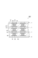
- FIGS. 1, 2 and FIG. 3 are cross-sectional views showing an embodiment of a semiconductor device that can be manufactured by the method according to the embodiment described later, respectively.
- FIG. 1 is a schematic cross-sectional view showing a COB type connection mode of a semiconductor chip and a substrate.
- the semiconductor device 100 shown in FIG. 1 includes a semiconductor chip 1 and a substrate 2 (wiring circuit board), and an adhesive layer 40 interposed between them.
- the semiconductor chip 1 is a semiconductor chip main body 10, a wiring or a bump 15 arranged on the surface of the semiconductor chip main body 10 on the substrate 2 side, and a connection portion arranged on the wiring or the bump 15. Has a solder 30 and.
- the substrate 2 has a substrate main body 20 and wiring or bumps 16 as connection portions arranged on the surface of the substrate main body 20 on the semiconductor chip 1 side.
- the solder 30 of the semiconductor chip 1 and the wiring or bump 16 of the substrate 2 are electrically connected by metal bonding.
- the semiconductor chip 1 and the substrate 2 are flip-chip connected by wiring or bumps 16 and solder 30.
- the wiring or bumps 15, 16 and the solder 30 are sealed from the external environment by being sealed by the adhesive layer 40.
- FIG. 2 shows a COC type connection mode between semiconductor chips.
- the configuration of the semiconductor device 300 shown in FIG. 2 is the same as that of the semiconductor device 100, except that the two semiconductor chips 1 are flip-chip connected via wiring or bumps 15 and solder 30.
- connection portion of the wiring or the bump 15 or the like may be a metal film called a pad (for example, gold plating) or a post electrode (for example, a copper pillar).
- the semiconductor chip main body 10 is not particularly limited, and various semiconductors such as elemental semiconductors composed of elements of the same type such as silicon and germanium, and compound semiconductors such as gallium arsenide and indium phosphorus can be used.
- the substrate 2 is not particularly limited as long as it is a wiring circuit board, and does not require a metal layer formed on the surface of an insulating substrate containing glass epoxy, polyimide, polyester, ceramic, epoxy, bismaleimide triazine and the like as main components.
- a circuit board on which wiring (wiring pattern) is formed by removing etching at a location a circuit board on which wiring (wiring pattern) is formed by metal plating or the like on the surface of the insulating substrate, and a conductive substance on the surface of the insulating substrate.
- a circuit board or the like on which wiring (wiring pattern) is formed by printing can be used.
- the main components are gold, silver, copper, and solder (main components are, for example, tin-silver, tin-lead, tin-bismuth, tin-. Copper, tin-silver-copper), tin, nickel and the like are used and may be composed of only a single component or may be composed of a plurality of components.
- the connecting portion may have a structure in which these metals are laminated. Of the metal materials, copper and solder are relatively inexpensive and preferable. From the viewpoint of improving connection reliability and suppressing warpage, the connection portion may contain solder.
- the main components of the pad are gold, silver, copper, solder (main components are, for example, tin-silver, tin-lead, tin-bismuth, tin-copper, tin-silver-copper), tin, and nickel. Etc. may be used and may be composed of only a single component or may be composed of a plurality of components.
- the pad may have a structure in which these metals are laminated. From the viewpoint of connection reliability, the pad may contain gold or solder.
- a metal layer containing the above as a main component may be formed.
- This metal layer may be composed of only a single component, or may be composed of a plurality of components.
- the metal layer may have a structure in which a plurality of metal layers are laminated.
- the metal layer may contain relatively inexpensive copper or solder. From the viewpoint of improving connection reliability and suppressing warpage, the metal layer may contain solder.
- the semiconductor devices (packages) as shown in FIGS. 1 or 2 are laminated, and gold, silver, copper, and solder (main components are, for example, tin-silver, tin-lead, tin-bismuth, tin-copper, tin). -Silver-copper), tin, nickel, etc. may be electrically connected.
- the metal for connection may be relatively inexpensive copper or solder.
- an adhesive layer may be flip-chip connected or laminated between semiconductor chips to form holes penetrating the semiconductor chips and connected to the electrodes on the patterned surface.
- FIG. 3 is a cross-sectional view showing another embodiment of the semiconductor device (semiconductor chip laminated type mode (TSV)).
- TSV semiconductor chip laminated type mode
- the wiring or bump 15 formed on the interposer main body 50 as a substrate is connected to the solder 30 of the semiconductor chip 1, so that the semiconductor chip 1 and the interposer 5 are flip-chips. It is connected.
- An adhesive layer 40 is interposed between the semiconductor chip 1 and the interposer 5.
- the semiconductor chip 1 is repeatedly laminated on the surface of the semiconductor chip 1 opposite to the interposer 5 via wiring or bumps 15, solder 30, and an adhesive layer 40.
- the wiring or bumps 15 on the pattern surface on the front and back of the semiconductor chip 1 are connected to each other by a through electrode 34 filled in a hole penetrating the inside of the semiconductor chip main body 10.
- a through electrode 34 filled in a hole penetrating the inside of the semiconductor chip main body 10.
- the material of the through electrode 34 copper, aluminum, or the like can be used.
- the adhesive layer can be applied as a sealing material between the semiconductor chips 1 facing each other and between the semiconductor chips 1 and the interposer 5.
- a first member having a connecting portion and a second member having a connecting portion are arranged so that the connecting portion of the first member and the connecting portion of the second member face each other.
- the semiconductor adhesive is cured by applying heat under normal pressure or a pressurized atmosphere, and the cured semiconductor adhesive is used to cure the connection portion. It comprises a sealing step of sealing at least a part thereof.
- the first member is, for example, a wiring circuit board, a semiconductor chip or a semiconductor wafer
- the second member is a semiconductor chip.
- the laminated body obtained in the laminating step is heated to a temperature equal to or higher than the melting point of the connecting portions arranged facing each other under normal pressure or a pressurized atmosphere, so that the connecting portions arranged facing each other are electrically connected to each other. Join so that they are connected.
- the laminating step is, for example, a step of arranging a plurality of semiconductor chips on the stage and a step of arranging the plurality of semiconductor chips on the stage while heating the stage.
- a temporary fixing step another semiconductor chip is sequentially arranged via a semiconductor adhesive, and a plurality of laminated bodies (temporary fixed bodies) in which the semiconductor chip, the semiconductor adhesive, and other semiconductor chips are laminated in this order are obtained. And, including.
- the laminating step is, for example, a step of arranging the wiring circuit board or the semiconductor wafer on the stage and a stage while heating the stage.
- a plurality of semiconductor chips are sequentially arranged on the wiring circuit board or the semiconductor wafer arranged above via the semiconductor adhesive, and the wiring circuit board, the semiconductor adhesive and the plurality of the semiconductor chips are laminated in this order.
- a temporary fixing step of obtaining a laminated body (temporary fixed body) or a laminated body (temporary fixed body) in which a semiconductor wafer, a semiconductor adhesive, and a plurality of the above-mentioned semiconductor chips are laminated in this order is included.
- a semiconductor adhesive is placed on the first member or the second member (for example, a film-shaped semiconductor adhesive is attached).
- the semiconductor chips separated on the dicing tape are picked up, adsorbed on the crimping tool (crimping head) of the crimping machine, and temporarily fixed to the wiring circuit board, another semiconductor chip, or the semiconductor wafer.
- the method of arranging the semiconductor adhesive is not particularly limited, and for example, when the semiconductor adhesive is in the form of a film, a method such as heat pressing, roll laminating, or vacuum laminating may be used.
- the area and thickness of the semiconductor adhesive to be arranged are appropriately set according to the sizes of the first member and the second member, the height of the connecting portion (bump), and the like.
- the semiconductor adhesive may be arranged on the semiconductor chip, or the semiconductor wafer on which the semiconductor adhesive is arranged may be diced and then individualized into the semiconductor chip.
- a crimping machine such as a flip chip bonder is generally used.
- the crimping tool When the crimping tool picks up the semiconductor chip for temporary fixing, it is preferable that the crimping tool has a low temperature so that heat is not transferred to the semiconductor adhesive or the like on the semiconductor chip.
- the semiconductor chip is heated to a high temperature so that the fluidity of the semiconductor adhesive can be increased and the entrained voids can be efficiently eliminated.
- heating at a lower temperature than the starting temperature of the curing reaction of the semiconductor adhesive is preferable.
- the difference between the temperature of the crimping tool when picking up the semiconductor chip and the temperature of the crimping tool at the time of temporary fixing is small.
- This temperature difference is preferably 100 ° C. or lower, more preferably 60 ° C. or lower, and even more preferably substantially 0 ° C. If the temperature difference is 100 ° C. or higher, it takes time to cool the crimping tool, so that the productivity tends to decrease.
- the starting temperature of the curing reaction of the semiconductor adhesive is measured using DSC (PerkinElmer Co., Ltd., DSC-Pyrs1) under the conditions of a sample amount of 10 mg, a temperature rise rate of 10 ° C./min, and an air or nitrogen atmosphere. The onset temperature of.
- the load applied for temporary fixing is appropriately set in consideration of control of the number of connecting portions (bumps), absorption of height variation of the connecting portions (bumps), deformation amount of the connecting portions (bumps), and the like.
- the connecting portions facing each other are in contact with each other after crimping (temporary crimping).
- temporary crimping temporary crimping
- the load is preferably large because of the elimination of voids and contact of the connection portion, for example, 0.0001N to 0.2N, preferably 0.009N to 0.2N per one connection portion (for example, a bump). Is more preferable, and 0.001 to 0.1N is even more preferable.
- the crimping time in the temporary fixing step is preferably as short as possible from the viewpoint of improving productivity, and may be, for example, 5 seconds or less, 3 seconds or less, or 2 seconds or less.
- the heating temperature of the stage is lower than the melting point of the connection portion of the first member and the melting point of the connection portion of the second member, and is usually 60 to 155 ° C, 65 to 120 ° C, or 70 to 100 ° C. It may be there. By heating at such a temperature, voids caught in the semiconductor adhesive can be efficiently eliminated. The heating temperature of the stage is not actually added to the adhesive itself.
- the temperature of the crimping tool at the time of temporary fixing is preferably set so that the temperature difference from the temperature of the crimping tool at the time of picking up the semiconductor chip becomes small as described above, but for example, it is 80 to 350 ° C. or , 100-170 ° C.
- the laminating step includes the temporary fixing step
- the sealing step following the temporary fixing step the semiconductor adhesive in the laminated body having a plurality of laminated bodies or a plurality of semiconductor chips is cured in a batch or divided manner, and a plurality of layers are cured.
- the connection portions may be collectively or divided and sealed.
- the sealing step the opposing connections are joined by metal bonding and the gaps between the connections are usually filled with a semiconductor adhesive.
- the sealing step is performed using a device capable of heating above the melting point of the metal of the connecting portion and capable of pressurizing. Examples of the apparatus include a pressure reflow furnace and a pressure oven.
- the heating temperature (connection temperature) in the sealing step is preferably a temperature equal to or higher than the melting point of at least one of the opposing connection portions (for example, bump-bump, bump-pad, bump-wiring).
- connection temperature a temperature equal to or higher than the melting point of at least one of the opposing connection portions (for example, bump-bump, bump-pad, bump-wiring).
- the metal of the connecting portion is solder, it is preferably 200 ° C. or higher and 450 ° C. or lower. If the heating temperature is low, the metal at the connection portion may not melt and sufficient metal bonds may not be formed. If the heating temperature is excessively high, the effect of suppressing voids tends to be relatively small, and the solder tends to scatter easily.
- the pressurization in the sealing step is performed not by the crimping machine but by the air pressure in the pressurizing reflow furnace, the pressurizing oven, or the like. If the pressurization is performed by atmospheric pressure, heat can be applied to the whole, and the heat treatment after crimping (main crimping) can be shortened or eliminated, and the productivity is improved.
- the pressure is applied by atmospheric pressure, it is easy to perform the main crimping of a plurality of laminated bodies (temporarily fixed body) or a laminated body (temporarily fixed body) including a plurality of temporarily fixed semiconductor chips at once.
- pressurization by atmospheric pressure is preferable from the viewpoint of fillet suppression, rather than direct pressurization using a crimping machine. Fillet suppression is important for the tendency of semiconductor devices to become smaller and denser.
- the atmosphere in which crimping is performed in the sealing step is not particularly limited, but an atmosphere containing air, nitrogen, formic acid, etc. is preferable.
- the crimping pressure in the sealing process is appropriately set according to the size and number of members to be connected.
- the pressure may be, for example, above atmospheric pressure and 1 MPa or less.
- a large pressure is preferable from the viewpoint of void suppression and connectivity improvement, and a small pressure is preferable from the viewpoint of fillet suppression. Therefore, the pressure is more preferably 0.05 to 0.5 MPa.
- the crimping time varies depending on the constituent metal of the connecting portion, but it is preferable that the crimping time is short from the viewpoint of improving productivity.
- the connection time is preferably 20 seconds or less, more preferably 10 seconds or less, still more preferably 5 seconds or less.
- the connection time is preferably 60 seconds or less.
- a plurality of semiconductor chips are three-dimensionally stacked, such as a semiconductor device having a TSV structure
- the plurality of semiconductor chips are stacked one by one to be temporarily fixed, and then the stacked semiconductor chips are collectively stacked. Then, the semiconductor device may be obtained by heating and pressurizing.
- the weight average molecular weight (Mw) of the component is obtained by the GPC method.
- the details of the GPC method are as follows.
- thermoplastic resin, the thermosetting resin, the curing agent, the organic acid and the filler shown in Table 1 (unit: parts by mass) are set to NV values ([Paint content mass after drying] / [Paint content mass before drying]. ] ⁇ 100) was added to the organic solvent (cyclohexanone) so as to be 50%. After that, ⁇ 1.0 mm zirconia beads and ⁇ 2.0 mm zirconia beads having the same mass as the amount of solid content (thermoplastic resin, thermosetting resin, curing agent, organic acid and filler) were added into the same container, and a ball mill was added. The mixture was stirred for 30 minutes with (Fritsch Japan Co., Ltd., planetary pulverizer P-7). After stirring, the zirconia beads were removed by filtration to prepare a coated varnish.
- the obtained coating varnish is coated on a base film (manufactured by Teijin DuPont Film Co., Ltd., trade name "Purex A55") with a small precision coating device (manufactured by Yasui Seiki Co., Ltd.) in a clean oven (manufactured by Yasui Seiki Co., Ltd.).
- a film-like adhesive having a film thickness of 20 ⁇ m was obtained by drying (manufactured by ESPEC) at 100 ° C./10 min.
- ⁇ DSC measurement> The obtained film-like adhesive was weighed in an aluminum pan (manufactured by Epolide Service Co., Ltd.) in an amount of 10 mg, covered with an aluminum lid, and the evaluation sample was sealed in the sample pan using a crimper. Using a differential scanning calorimeter (Thermo plus DSC8235E, manufactured by Rigaku Co., Ltd.), measurements were taken under a nitrogen atmosphere at a heating rate of 10 ° C./min and a measurement temperature range of 30 to 300 ° C.
- an analysis method for the entire area (JIS method) is used, and by instructing analysis in the temperature range of 60 to 250 ° C., the intersection of the peak baseline and the maximum slope point in each DSC curve is determined. The onset temperature (unit: ° C.) was calculated.
- the analysis method for the entire area (JIS method) is also used, and the calorific value is integrated by integrating the peaks in each DSC curve by instructing the analysis in the temperature range of 60 to 250 ° C. (Unit: J / g) was calculated.
- a differential scanning calorimeter (Thermo plus DSC8235E, manufactured by Rigaku Co., Ltd.) was used in the same procedure as before the heat treatment, and the calorific value (unit: J / g) at 60 to 250 ° C. was calculated. This was taken as the calorific value after the heat treatment.
- reaction rate was calculated by the following formula using the two calorific values obtained (the calorific value of the initial sample and the calorific value of the evaluation sample A).
- Reaction rate (%) (initial calorific value-calorific value after heat treatment) / initial calorific value x 100
- the laminated body (temporary fixed body C) after the temporary crimping was placed in an oven set at 80 ° C., heat-treated for 6 hours, then a sample was taken out, and the laminated body D (temporary fixed body C) after the temporary crimping after heat treatment at 80 ° C. Fixed body D) was obtained.
- the laminated body D (temporary fixed body D) after the temporary crimping was placed in the oven of a pressurized oven device (manufactured by NTT Advanced Technology Corporation).
- the pressure in the oven was set to 0.8 MPa, and the temperature was raised from room temperature to 190 ° C. at a heating rate of 20 ° C./min.
- the pressure-bonded body was heated for 1 hour in a pressurized atmosphere while maintaining the pressure and temperature to obtain a mounting sample E for evaluation.
- an image of the adhesive layer between the chips was captured by a scanner (GT-9300UF, manufactured by Seiko Epson Corporation).
- the void portion was identified by color tone correction and two-gradation using image processing software (Adobe Photoshop (trade name)), and the proportion of the void portion was calculated from the histogram.
- the area of the entire adhesive layer including the void portion was set to 100 area%. When the area ratio of voids was less than 10%, it was designated as "A”, when the area ratio of voids was 10% or more and less than 30%, it was designated as "B”, and when it was 30% or more, it was designated as "C”. Table 1 shows the evaluation results.
- the crimping conditions are 190 ° C / 25N / 10 seconds, 260 ° C / 25N / 20 seconds, 100 ° C / 25N / 5 seconds (set temperature rise time at each temperature rise: 0.1 seconds), and heat is applied step by step. It was crimped while hanging.
- the laminated body F (temporary fixed body F) after the temporary crimping was placed in the oven of a pressurized oven device (manufactured by NTT Advanced Technology Corporation).
- the pressure in the oven was set to 0.8 MPa, and the temperature was raised from room temperature to 190 ° C. at a heating rate of 20 ° C./min.
- the pressure-bonded body was heated for 1 hour in a pressurized atmosphere while maintaining the pressure and temperature to obtain a mounting sample G for evaluation.
- the above evaluation mounting sample was polished using a tabletop grinding machine (Refine Polisher, manufactured by Refine Tech Co., Ltd.) until the bump connection part existing inside the chip was exposed.
- a water-resistant polishing paper having a size of 200 cm ⁇ and a particle size of 1000 was first used, and then the paper was replaced with a water-resistant polishing paper having a particle size of 2000, and then polished until the connection portion was exposed. Then, it was further polished with an alumina solution (suspended solution) A-0.3 micron (manufactured by Refine Tech Co., Ltd.).
- the exposed bump connection portion was observed with an SEM (TM3030Plus desktop microscope, manufactured by Hitachi High-Technologies Corporation), and the presence or absence of cracks in the solder interior and the solder-Cu wiring interface was confirmed.
- the connectivity of the obtained mounting sample G for evaluation was evaluated by measuring the resistance value of the inner circumference of the chip using a circuit tester (POCKET TESTER 4300 COUNT, manufactured by CUSTOM).
- Lower chip used for mounting chip size: 7.3 mm x 7.3 mm, thickness 0.1 mm, bump (connection) height: about 45 ⁇ m (total of copper pillar and solder), number of bumps: 1048 pins, pitch
- the circuit diagram of 80 ⁇ m, product name: WALTS-TEG CC80, manufactured by Waltz Co., Ltd.) is shown in FIG.
- the resistance value between the terminal a and the terminal b in the figure is the resistance value on the inner circumference of the chip. If the value of this resistance value is less than 35 ⁇ , it indicates that the connection is good, and if it is 35 ⁇ or more or the resistance value cannot be measured, it indicates that the connection is poor.
Landscapes
- Chemical & Material Sciences (AREA)
- Organic Chemistry (AREA)
- Health & Medical Sciences (AREA)
- Chemical Kinetics & Catalysis (AREA)
- Medicinal Chemistry (AREA)
- Polymers & Plastics (AREA)
- Adhesives Or Adhesive Processes (AREA)
- Wire Bonding (AREA)
- Structures Or Materials For Encapsulating Or Coating Semiconductor Devices Or Solid State Devices (AREA)
Abstract
熱可塑性樹脂、熱硬化性樹脂、硬化剤及び有機酸を含む半導体用接着剤であって、有機酸は、酸性官能基を2個以上有する、酸解離定数pKaが4.0以下の化合物である、半導体用接着剤。
Description
本開示は、半導体用接着剤、並びに、半導体装置及びその製造方法に関する。
従来、半導体チップと基板とを接続するには、金ワイヤ等の金属細線を用いるワイヤーボンディング方式が広く適用されてきた。
近年、半導体装置に対する高機能化、高集積化、高速化等の要求に対応するため、半導体チップ又は基板にバンプと呼ばれる導電性突起を形成して、半導体チップと基板とを直接接続するフリップチップ接続方式(FC接続方式)が広まりつつある。
例えば、半導体チップ及び基板間の接続に関して、BGA(Ball Grid Array)、CSP(Chip Size Package)等に盛んに用いられているCOB(Chip On Board)型の接続方式もFC接続方式に該当する。また、FC接続方式は、半導体チップ上に接続部(バンプ又は配線)を形成して、半導体チップ間を接続するCOC(Chip On Chip)型、及び、半導体ウェハ上に接続部(バンプ又は配線)を形成して、半導体チップと半導体ウェハとの間を接続するCOW(Chip On Wafer)型の接続方式にも広く用いられている(例えば、特許文献1参照)。
また、さらなる小型化、薄型化及び高機能化が強く要求されるパッケージでは、上述した接続方式を積層・多段化したチップスタック型パッケージ、POP(Package On Package)、TSV(Through-Silicon Via)等も広く普及し始めている。このような積層・多段化技術は、半導体チップ等を三次元的に配置することから、二次元的に配置する手法と比較してパッケージを小さくできる。また、積層・多段化技術は、半導体の性能向上、ノイズ低減、実装面積の削減、省電力化等にも有効であることから、次世代の半導体配線技術として注目されている。
近年、生産性を向上させる観点から、半導体用接着剤を介して複数の半導体チップを被搭載部材(半導体チップ、半導体ウェハ、配線回路基板等)の上に搭載し仮固定した後、一括もしくは分割して硬化と封止を行うプロセスが提案されている。このプロセスでは、半導体用接着剤が流動可能な程度にステージに熱(60~155℃程度)を加えることで、被搭載部材に半導体チップを仮固定した後、接続部の融点以上の温度(例えば260℃程度)でリフローもしくは本圧着することで、半導体用接着剤を一括もしくは分割して硬化する。このプロセスによれば、複数個のパッケージを効率良く作製することができる。
上記プロセスでは、半導体チップが順次搭載されるため、初期に搭載された半導体チップ及び半導体用接着剤に対しては、最後の半導体チップの搭載が完了するまでステージによる熱履歴が与えられ続けることとなる。そのため、半導体チップの数が多くなると、初期に搭載された半導体チップを仮固定する半導体用接着剤の硬化が部分的に進行してしまい、一括硬化時の加圧によって、ボイドが除去されずに残存する傾向がある。この問題を改善するために、半導体用接着剤には、優れた耐熱履歴性を有すること、すなわち、仮固定時の熱履歴による硬化反応の進行を抑制できることが求められる。
そこで、本開示は、熱履歴後反応率を低減することができる半導体用接着剤を提供することを目的とする。また、本開示は、上記半導体用接着剤を用いた半導体装置及びその製造方法を提供することを目的とする。
上記目的を達成するために、本開示は、熱可塑性樹脂、熱硬化性樹脂、硬化剤及び有機酸を含む半導体用接着剤であって、上記有機酸は、酸性官能基を2個以上有する、酸解離定数pKaが4.0以下の化合物である、半導体用接着剤を提供する。
上記有機酸は、酸性官能基を2個以上有し、且つ、酸解離定数pKaが4.0以下であることにより、上記硬化剤の少なくとも一部と強固な塩を形成することができる。そして、硬化剤と有機酸とが塩を形成することで、硬化剤と熱硬化性樹脂との反応を阻害することができる。そのため、上記有機酸を含む半導体用接着剤によれば、仮固定時の熱履歴により上記硬化剤と上記熱硬化性樹脂との硬化反応が進行することを抑制し、熱履歴後反応率を低減することができる。なお、本圧着時には、仮固定時のステージによる熱履歴よりも高い温度の熱が加えられることによって、塩を形成していた硬化剤と有機酸とが分離する。これにより、本圧着時には、分離した硬化剤と上記熱硬化性樹脂とが反応し、ボイドの残存が抑制された半導体装置を得ることができる。
上記酸性官能基は、カルボキシル基、スルホキシル基及びリン酸基からなる群より選択される少なくとも一種の基を含んでいてよい。上記酸性官能基は、上記硬化剤に含まれる塩基性官能基と塩形成できる酸性官能基であれば特に制限されず、上記有機酸は、複数種の酸性官能基を含んでいてもよい。
上記硬化剤に含まれる塩基性官能基に対する、上記有機酸に含まれる上記酸性官能基の当量比が1.0以上であってよい。当該当量比が1.0以上であることにより、本圧着前に有機酸と反応していない硬化剤の量が低減し、当該当量比が1.0未満であるときよりも、熱履歴後反応率を低減することができる。
上記有機酸は、下記一般式(1-1)、(1-2)又は(1-3)で表される化合物を含んでいてよい。


[式(1-1)、(1-2)及び(1-3)中、R1は電子吸引性基を示し、R2は水素原子又は電子吸引性基を示し、R3は水素原子又は1価の有機基を示し、Xは酸素原子又は硫黄原子を示し、n1は0~15の整数を示し、n2及びn3はそれぞれ、n2+n3が2~15の整数となるように選ばれる1以上の整数を示し、mは1又は2を示す。なお、複数存在するR3は互いに同一でも異なっていてもよい。]
上記有機酸の融点は、50~250℃であってよい。このような有機酸は、熱硬化性樹脂と硬化剤との硬化反応が生じる前にフラックス活性が充分に発現するため、当該有機酸を含有する半導体用接着剤によれば、接続信頼性に一層優れる半導体装置を実現できる。
上記硬化剤は、アミン系硬化剤を含んでいてよい。このような化合物は、熱硬化性樹脂と硬化剤との硬化反応により優れた硬化特性を発現させ、半導体装置の耐リフロー性を一層向上させることができる。
上記硬化剤は、イミダゾール系硬化剤を含んでいてよい。このような化合物を用いることで、半導体用接着剤の安定性を一層向上させることができる。
上記イミダゾール系硬化剤の構造は、トリアジン環を含む構造であってよい。このような化合物を用いることで、半導体用接着剤の安定性を一層向上させることができる。
本開示はまた、半導体チップ及び配線回路基板のそれぞれの接続部が互いに電気的に接続された半導体装置、又は、複数の半導体チップのそれぞれの接続部が互いに電気的に接続された半導体装置の製造方法であって、上記本開示の半導体用接着剤を、常圧又は加圧雰囲気下で熱を加えることにより硬化させ、硬化した上記半導体用接着剤により上記接続部の少なくとも一部を封止する封止工程を備える、半導体装置の製造方法を提供する。
上記製造方法は、上記封止工程の前に、ステージ上に複数の半導体チップを配置する工程と、上記ステージを60~155℃に加熱しながら、上記ステージ上に配置された上記複数の半導体チップのそれぞれの上に、上記半導体用接着剤を介して他の半導体チップを順次配置し、上記半導体チップ、上記半導体用接着剤及び上記他の半導体チップがこの順に積層されてなる積層体を複数得る仮固定工程と、を更に備えていてよい。
あるいは、上記製造方法は、上記封止工程の前に、ステージ上に配線回路基板又は半導体ウェハを配置する工程と、上記ステージを60~155℃に加熱しながら、上記ステージ上に配置された上記配線回路基板又は半導体ウェハの上に、上記半導体用接着剤を介して複数の半導体チップを順次配置し、上記配線回路基板、上記半導体用接着剤及び複数の上記半導体チップがこの順に積層されてなる積層体、又は、上記半導体ウェハ、上記半導体用接着剤及び複数の上記半導体チップがこの順に積層されてなる積層体を得る仮固定工程と、を更に備えていてよい。
本開示は更に、半導体チップ及び配線回路基板のそれぞれの接続部が互いに電気的に接続された半導体装置、又は、複数の半導体チップのそれぞれの接続部が互いに電気的に接続された半導体装置であって、上記接続部の少なくとも一部が、常圧又は加圧雰囲気下で熱を加えて硬化された上記本開示の半導体用接着剤の硬化物によって封止されている、半導体装置を提供する。
本開示によれば、半導体用接着剤を介して複数の半導体チップを被搭載部材上に仮固定し、一括して硬化と封止を行うプロセスにおいて、半導体用接着剤中に残存し得るボイドを低減することができる。本開示によれば、このようなボイドを低減することができると共に、接続性に優れる半導体装置の作製を可能とする半導体用接着剤、並びに、当該半導体用接着剤を用いた半導体装置及びその製造方法を提供することができる。
以下、場合により図面を参照しつつ本開示の一実施形態について詳細に説明する。なお、図面中、同一又は相当部分には同一符号を付し、重複する説明は省略する。また、上下左右等の位置関係は、特に断らない限り、図面に示す位置関係に基づくものとする。さらに、図面の寸法比率は図示の比率に限られるものではない。
本明細書に記載される数値範囲の上限値及び下限値は、任意に組み合わせることができる。実施例に記載される数値も、数値範囲の上限値又は下限値として用いることができる。本明細書において、「(メタ)アクリル」とは、アクリル又はそれに対応するメタクリルを意味する。
<半導体用接着剤及びその製造方法>
本実施形態の半導体用接着剤は、熱可塑性樹脂(以下、場合により「(a)成分」という。)、熱硬化性樹脂(以下、場合により「(b)成分」という。)、硬化剤(以下、場合により「(c)成分」という。)及び有機酸(以下、場合により「(d)成分」という。)を含有する。本実施形態の半導体用接着剤は、必要に応じて、フィラー(以下、場合により「(e)成分」という。)を含有していてもよい。
本実施形態の半導体用接着剤は、熱可塑性樹脂(以下、場合により「(a)成分」という。)、熱硬化性樹脂(以下、場合により「(b)成分」という。)、硬化剤(以下、場合により「(c)成分」という。)及び有機酸(以下、場合により「(d)成分」という。)を含有する。本実施形態の半導体用接着剤は、必要に応じて、フィラー(以下、場合により「(e)成分」という。)を含有していてもよい。
本実施形態の半導体用接着剤の示差走査熱量測定(DSC:Differential scanning calorimetry)により得られるDSC曲線の60~155℃の発熱量は、20J/g以下であってよい。ここで、示差走査熱量測定は、サンプルとなる半導体用接着剤の重量を10mgとし、測定温度範囲を30~300℃とし、昇温速度を10℃/minとして、空気又は窒素雰囲気で半導体用接着剤を加熱することにより行う。発熱量は、ピーク面積の積分により算出される。
従来の半導体用接着剤は、DSC曲線の60~155℃の温度領域に発熱ピークを有している。この温度領域における発熱は、半導体用接着剤中の熱硬化性樹脂と有機酸の反応に由来する発熱であると推察され、この反応が進行すると、半導体用接着剤が部分的に硬化し、流動性が低下すると推察される。一方、通常、半導体用接着剤による半導体チップの仮固定は、半導体用接着剤を例えば60~155℃に加熱して適度に流動させることにより行われる。したがって、半導体用接着剤を介して複数の半導体チップを被搭載部材(半導体チップ、半導体ウェハ、配線回路基板等)の上に搭載し仮固定した後、加圧条件下で一括して硬化と封止を行うプロセスにおいて従来の半導体用接着剤を用いると、半導体チップを仮固定する際に、半導体用接着剤中の熱硬化性樹脂と有機酸とが反応することで、半導体用接着剤の硬化が部分的に進行し、加圧条件下での一括硬化時に充分に流動しなくなる場合があると推察される。一方、本実施形態の半導体用接着剤において、DSC曲線の60~155℃の発熱量が20J/g以下である場合、上記半導体チップの仮固定を行う温度領域(例えば60~155℃)において硬化が進行し難い。そのため、上記プロセスにおいて上記発熱量の条件を満たす半導体用接着剤を用いることで、半導体用接着剤の充分な流動性を維持しながら複数の半導体チップを仮固定することができ、一括硬化時のボイドの発生を低減することが可能となる。さらに、ボイドの発生が低減される結果、リフロー工程において接続部の融点以上の温度(例えば260℃)で加熱したとしても、不具合(半導体用接着剤の剥離、接続部での電気的な接続不良等)が起こり難くなることが期待される。すなわち、上記発熱量の条件を満たす半導体用接着剤によれば、半導体装置の製造におけるリフロー信頼性(耐リフロー性)を向上させることができる傾向がある。
上記DSC曲線の60~155℃の発熱量は、本発明の効果が得られやすい観点から、15J/g以下が好ましく、10J/g以下がより好ましく、5J/g以下が更に好ましい。上記DSC曲線の60~155℃の発熱量は、本発明の効果が得られやすい観点から、60~280℃の発熱量の20%以下、15%以下又は10%以下であってよい。上記DSC曲線の60~280℃の発熱量は、本発明の効果が得られやすい観点から、50J/g以上又は100J/g以上であってよく、200J/g以下又は180J/g以下であってよく、50~200J/g、100~200J/g又は100~180J/gであってよい。上記DSC曲線は、本発明の効果が得られやすい観点から、オンセット温度が155℃以下にある発熱ピークを有しないことが好ましい。
以下、本実施形態の半導体用接着剤を構成する各成分について説明する。
(a)熱可塑性樹脂
(a)成分としては、特に限定されるものではないが、例えば、フェノキシ樹脂、ポリイミド樹脂、ポリアミド樹脂、ポリカルボジイミド樹脂、シアネートエステル樹脂、アクリル樹脂、ポリエステル樹脂、ポリエチレン樹脂、ポリエーテルスルホン樹脂、ポリエーテルイミド樹脂、ポリビニルアセタール樹脂、ウレタン樹脂及びアクリルゴムが挙げられる。これらの中でも耐熱性及びフィルム形成性に優れる観点から、フェノキシ樹脂、ポリイミド樹脂、アクリル樹脂、アクリルゴム、シアネートエステル樹脂及びポリカルボジイミド樹脂が好ましく、フェノキシ樹脂、ポリイミド樹脂及びアクリル樹脂がより好ましい。これらの(a)成分は単独で使用することができ、2種以上の混合物又は共重合体として使用することもできる。
(a)成分としては、特に限定されるものではないが、例えば、フェノキシ樹脂、ポリイミド樹脂、ポリアミド樹脂、ポリカルボジイミド樹脂、シアネートエステル樹脂、アクリル樹脂、ポリエステル樹脂、ポリエチレン樹脂、ポリエーテルスルホン樹脂、ポリエーテルイミド樹脂、ポリビニルアセタール樹脂、ウレタン樹脂及びアクリルゴムが挙げられる。これらの中でも耐熱性及びフィルム形成性に優れる観点から、フェノキシ樹脂、ポリイミド樹脂、アクリル樹脂、アクリルゴム、シアネートエステル樹脂及びポリカルボジイミド樹脂が好ましく、フェノキシ樹脂、ポリイミド樹脂及びアクリル樹脂がより好ましい。これらの(a)成分は単独で使用することができ、2種以上の混合物又は共重合体として使用することもできる。
(a)成分の重量平均分子量(Mw)は、好ましくは10000以上であり、40000以上であることがより好ましく、60000以上であることが更に好ましい。このような(a)成分によれば、フィルム形成性及び接着剤の耐熱性を一層向上させることができる。また、重量平均分子量が10000以上であると、フィルム状の半導体用接着剤に柔軟性を付与しやすいため、一層優れた加工性が得られやすい。また、(a)成分の重量平均分子量は、1000000以下であることが好ましく、500000以下であることがより好ましい。このような(a)成分によれば、フィルムの粘度が低下するため、バンプへの埋め込み性が良好になり、より一層ボイド無く実装することができる。これらの観点から、(a)成分の重量平均分子量は、10000~1000000が好ましく、40000~500000がより好ましく、60000~500000が更に好ましい。
なお、本明細書において、上記重量平均分子量とは、GPC(ゲル浸透クロマトグラフィー、Gel Permeation Chromatography)を用いて測定された、ポリスチレン換算の重量平均分子量を示す。GPC法の測定条件の一例を以下に示す。
装置:HCL-8320GPC、UV-8320(製品名、東ソー株式会社製)、又はHPLC-8020(製品名、東ソー株式会社製)
カラム:TSKgel superMultiporeHZ-M×2、又は2pieces of GMHXL + 1piece of G-2000XL
検出器:RI又はUV検出器
カラム温度:25~40℃
溶離液:高分子成分が溶解する溶媒を選択する。溶媒としては、例えば、THF(テトラヒドロフラン)、DMF(N,N-ジメチルホルムアミド)、DMA(N,N-ジメチルアセトアミド)、NMP(N-メチルピロリドン)、トルエン等が挙げられる。なお、極性を有する溶剤を選択する場合は、リン酸の濃度を0.05~0.1mol/L(通常は0.06mol/L)、LiBrの濃度を0.5~1.0mol/L(通常は0.63mol/L)と調整してもよい。
流速:0.30~1.5mL/分
標準物質:ポリスチレン
装置:HCL-8320GPC、UV-8320(製品名、東ソー株式会社製)、又はHPLC-8020(製品名、東ソー株式会社製)
カラム:TSKgel superMultiporeHZ-M×2、又は2pieces of GMHXL + 1piece of G-2000XL
検出器:RI又はUV検出器
カラム温度:25~40℃
溶離液:高分子成分が溶解する溶媒を選択する。溶媒としては、例えば、THF(テトラヒドロフラン)、DMF(N,N-ジメチルホルムアミド)、DMA(N,N-ジメチルアセトアミド)、NMP(N-メチルピロリドン)、トルエン等が挙げられる。なお、極性を有する溶剤を選択する場合は、リン酸の濃度を0.05~0.1mol/L(通常は0.06mol/L)、LiBrの濃度を0.5~1.0mol/L(通常は0.63mol/L)と調整してもよい。
流速:0.30~1.5mL/分
標準物質:ポリスチレン
(a)成分の含有量Caに対する(b)成分の含有量Cbの比Cb/Ca(質量比)は、好ましくは0.01以上、より好ましくは0.1以上、更に好ましくは1以上であり、好ましくは5以下、より好ましくは4.5以下、更に好ましくは4以下である。比Cb/Caを0.01以上とすることで、より良好な硬化性及び接着力が得られ、比Cb/Caを5以下とすることでより良好なフィルム形成性が得られる。これらの観点から、比Cb/Caは0.01~5であることが好ましく、0.1~4.5であることがより好ましく、1~4であることが更に好ましい。
(a)成分のガラス転移温度は、接続信頼性の向上等の観点から、好ましくは-50℃以上、より好ましくは-40℃以上、更に好ましくは-30℃以上であり、ラミネート性等の観点から、好ましくは220℃以下、より好ましくは200℃以下、更に好ましくは180℃以下である。(a)成分のガラス転移温度は、-50~220℃であることが好ましく、-40~200℃であることがより好ましく、-30~180℃であることが更に好ましい。このような(a)成分を含む半導体用接着剤によれば、ウェハレベルでの実装プロセスに際し、ウェハ反り量を一層低減することができると共に、半導体用接着剤の耐熱性及びフィルム形成性を一層向上させることができる。(a)成分のガラス転移温度は、示差走査熱量計(DSC)により測定することができる。
(a)成分の含有量は、半導体用接着剤の固形分全量を基準として、30質量%以下であることが好ましく、25質量%以下であることがより好ましく、20質量%以下であることが更に好ましい。(a)成分の含有量が30質量%以下であると、半導体用接着剤は温度サイクル試験の際に良好な信頼性を得ることができ、吸湿後でも260℃前後のリフロー温度で良好な接着力を得ることができる。また、(a)成分の含有量は、半導体用接着剤の固形分全量を基準として、1質量%以上であることが好ましく、3質量%以上であることがより好ましく、5質量%以上であることが更に好ましい。(a)成分の含有量が1質量%以上であると、半導体用接着剤はウェハレベルでの実装プロセスに際し、ウェハ反り量を一層低減することができると共に、半導体用接着剤の耐熱性及びフィルム形成性を一層向上させることができる。また、(a)成分の含有量が5質量%以上であると、ウェハ形状に外形加工する際のバリ及び欠けの発生を抑制することができる。(a)成分の含有量は、上記観点、及び、フィルム状の半導体用接着剤に柔軟性を付与しやすく、一層優れた加工性が得られやすい観点から、半導体用接着剤の固形分全量を基準として、1~30質量%が好ましく、3~30質量%がより好ましく、5~30質量%が更に好ましい。なお、「半導体用接着剤の固形分全量」とは、半導体用接着剤の全量から半導体用接着剤に含まれる溶媒の量を除いた量である。本明細書では、「半導体用接着剤の固形分全量」を、「(a)~(e)成分の合計量」と言い換えてもよい。
(b)熱硬化性樹脂
(b)成分としては、分子内に2個以上の反応基を有するものであれば特に制限なく用いることができる。半導体用接着剤が熱硬化性樹脂を含有することで、加熱により接着剤が硬化することができ、硬化した接着剤が高い耐熱性とチップへの接着力を発現し、優れた耐リフロー性が得られる。
(b)成分としては、分子内に2個以上の反応基を有するものであれば特に制限なく用いることができる。半導体用接着剤が熱硬化性樹脂を含有することで、加熱により接着剤が硬化することができ、硬化した接着剤が高い耐熱性とチップへの接着力を発現し、優れた耐リフロー性が得られる。
(b)成分としては、例えば、エポキシ樹脂、フェノール樹脂、イミド樹脂、ユリア樹脂、メラミン樹脂、シリコン樹脂、(メタ)アクリル化合物、ビニル化合物が挙げられる。これらの中でも耐熱性(耐リフロー性)及び保存安定性に優れる観点から、エポキシ樹脂、フェノール樹脂及びイミド樹脂が好ましく、エポキシ樹脂及びイミド樹脂がより好ましく、エポキシ樹脂が更に好ましい。これらの(b)成分は単独で使用することができ、2種以上の混合物又は共重合体として使用することもできる。従来の半導体用接着剤の中でも、特に、熱硬化性樹脂がエポキシ樹脂、メラミン樹脂又はユリア樹脂である場合に、60~155℃の温度領域で後述する有機酸との反応が進行しやすく、一括硬化の前に部分的な硬化が進行する傾向があるが、本実施形態では、熱硬化性樹脂がエポキシ樹脂、メラミン樹脂及びユリア樹脂からなる群より選択される少なくとも一種の樹脂を含む場合であっても、このような反応及び部分的な硬化が起こり難い。
エポキシ樹脂及びイミド樹脂としては、例えば、ビスフェノールA型エポキシ樹脂、ビスフェノールF型エポキシ樹脂、ナフタレン型エポキシ樹脂、フェノールノボラック型エポキシ樹脂、クレゾールノボラック型エポキシ樹脂、フェノールアラルキル型エポキシ樹脂、ビフェニル型エポキシ樹脂、トリフェニルメタン型エポキシ樹脂、ジシクロペンタジエン型エポキシ樹脂及び各種多官能エポキシ樹脂、ナジイミド樹脂、アリルナジイミド樹脂、マレイミド樹脂、アミドイミド樹脂、イミドアクリレート樹脂、各種多官能イミド樹脂及び各種ポリイミド樹脂を使用することができる。これらは単独で又は2種以上の混合物として使用することができる。
(b)成分は、高温での接続時に分解して揮発成分が発生することを抑制する観点から、接続時の温度が250℃の場合は、250℃における熱重量減少量率が5%以下のものを用いることが好ましく、接続時の温度が300℃の場合は、300℃における熱重量減少量率が5%以下のものを用いることが好ましい。
(b)成分の含有量は、半導体用接着剤の固形分全量を基準として、例えば5質量%以上であり、好ましくは15質量%以上であり、より好ましくは30質量%以上である。(b)成分の含有量は、半導体用接着剤の固形分全量を基準として、例えば80質量%以下であり、好ましくは70質量%以下であり、より好ましくは60質量%以下である。(b)成分の含有量は、半導体用接着剤の固形分全量を基準として、例えば、5~80質量%であり、好ましくは15~70質量%であり、より好ましくは30~60質量%である。
(c)硬化剤
(c)成分は、後述する有機酸と塩を形成することができる硬化剤であってよい。(c)成分としては、例えば、アミン系硬化剤(アミン類)及びイミダゾール系硬化剤(イミダゾール類)が挙げられる。(c)成分がアミン系硬化剤又はイミダゾール系硬化剤を含むと、接続部に酸化膜が生じることを抑制するフラックス活性を示し、接続信頼性・絶縁信頼性を向上させることができる。また、(c)成分がアミン系硬化剤又はイミダゾール系硬化剤を含むと、保存安定性が一層向上し、吸湿による分解又は劣化が起こりにくくなる傾向がある。さらに、(c)成分がアミン系硬化剤又はイミダゾール系硬化剤を含むと、硬化速度の調整が容易となり、また、速硬化性により生産性向上を目的とした短時間接続の実現が容易となる。
(c)成分は、後述する有機酸と塩を形成することができる硬化剤であってよい。(c)成分としては、例えば、アミン系硬化剤(アミン類)及びイミダゾール系硬化剤(イミダゾール類)が挙げられる。(c)成分がアミン系硬化剤又はイミダゾール系硬化剤を含むと、接続部に酸化膜が生じることを抑制するフラックス活性を示し、接続信頼性・絶縁信頼性を向上させることができる。また、(c)成分がアミン系硬化剤又はイミダゾール系硬化剤を含むと、保存安定性が一層向上し、吸湿による分解又は劣化が起こりにくくなる傾向がある。さらに、(c)成分がアミン系硬化剤又はイミダゾール系硬化剤を含むと、硬化速度の調整が容易となり、また、速硬化性により生産性向上を目的とした短時間接続の実現が容易となる。
以下、各硬化剤について説明する。
(i)アミン系硬化剤
アミン系硬化剤としては、例えばジシアンジアミドを使用することができる。
アミン系硬化剤としては、例えばジシアンジアミドを使用することができる。
アミン系硬化剤の含有量は、上記(b)成分100質量部に対して、好ましくは0.1質量部以上である。また、アミン系硬化剤の含有量は、上記(b)成分100質量部に対して、好ましくは10質量部以下であり、より好ましくは5質量部以下である。アミン系硬化剤の含有量が0.1質量部以上であると硬化性が向上する傾向があり、10質量部以下であると金属接合が形成される前に半導体用接着剤が硬化することがなく、接続不良が発生しにくい傾向がある。これらの観点から、アミン系硬化剤の含有量は、(b)成分100質量部に対して、0.1~10質量部が好ましく、0.1~5質量部がより好ましい。
(ii)イミダゾール系硬化剤
イミダゾール系硬化剤としては、例えば、2-フェニルイミダゾール、2-フェニル-4-メチルイミダゾール、1-ベンジル-2-メチルイミダゾール、1-ベンジル-2-フェニルイミダゾール、1-シアノエチル-2-ウンデシルイミダゾール、1-シアノ-2-フェニルイミダゾール、1-シアノエチル-2-ウンデシルイミダゾールトリメリテイト、1-シアノエチル-2-フェニルイミダゾリウムトリメリテイト、2,4-ジアミノ-6-[2’-メチルイミダゾリル-(1’)]-エチル-s-トリアジン、2,4-ジアミノ-6-[2’-ウンデシルイミダゾリル-(1’)]-エチル-s-トリアジン、2,4-ジアミノ-6-[2’-エチル-4’-メチルイミダゾリル-(1’)]-エチル-s-トリアジン、2,4-ジアミノ-6-[2’-メチルイミダゾリル-(1’)]-エチル-s-トリアジンイソシアヌル酸付加体、2-フェニルイミダゾールイソシアヌル酸付加体、2-フェニル-4,5-ジヒドロキシメチルイミダゾール、2-フェニル-4-メチル-5-ヒドロキシメチルイミダゾール、及び、エポキシ樹脂とイミダゾール類の付加体が挙げられる。これらの中でも、優れた硬化性、保存安定性及び接続信頼性の観点から、1-シアノエチル-2-ウンデシルイミダゾール、1-シアノ-2-フェニルイミダゾール、1-シアノエチル-2-ウンデシルイミダゾールトリメリテイト、1-シアノエチル-2-フェニルイミダゾリウムトリメリテイト、2,4-ジアミノ-6-[2’-メチルイミダゾリル-(1’)]-エチル-s-トリアジン、2,4-ジアミノ-6-[2’-エチル-4’-メチルイミダゾリル-(1’)]-エチル-s-トリアジン、2,4-ジアミノ-6-[2’-メチルイミダゾリル-(1’)]-エチル-s-トリアジンイソシアヌル酸付加体、2-フェニルイミダゾールイソシアヌル酸付加体、2-フェニル-4,5-ジヒドロキシメチルイミダゾール及び2-フェニル-4-メチル-5-ヒドロキシメチルイミダゾールが好ましい。これらは単独で又は2種以上を併用して用いることができる。また、これらをマイクロカプセル化した潜在性硬化剤としてもよい。
イミダゾール系硬化剤としては、例えば、2-フェニルイミダゾール、2-フェニル-4-メチルイミダゾール、1-ベンジル-2-メチルイミダゾール、1-ベンジル-2-フェニルイミダゾール、1-シアノエチル-2-ウンデシルイミダゾール、1-シアノ-2-フェニルイミダゾール、1-シアノエチル-2-ウンデシルイミダゾールトリメリテイト、1-シアノエチル-2-フェニルイミダゾリウムトリメリテイト、2,4-ジアミノ-6-[2’-メチルイミダゾリル-(1’)]-エチル-s-トリアジン、2,4-ジアミノ-6-[2’-ウンデシルイミダゾリル-(1’)]-エチル-s-トリアジン、2,4-ジアミノ-6-[2’-エチル-4’-メチルイミダゾリル-(1’)]-エチル-s-トリアジン、2,4-ジアミノ-6-[2’-メチルイミダゾリル-(1’)]-エチル-s-トリアジンイソシアヌル酸付加体、2-フェニルイミダゾールイソシアヌル酸付加体、2-フェニル-4,5-ジヒドロキシメチルイミダゾール、2-フェニル-4-メチル-5-ヒドロキシメチルイミダゾール、及び、エポキシ樹脂とイミダゾール類の付加体が挙げられる。これらの中でも、優れた硬化性、保存安定性及び接続信頼性の観点から、1-シアノエチル-2-ウンデシルイミダゾール、1-シアノ-2-フェニルイミダゾール、1-シアノエチル-2-ウンデシルイミダゾールトリメリテイト、1-シアノエチル-2-フェニルイミダゾリウムトリメリテイト、2,4-ジアミノ-6-[2’-メチルイミダゾリル-(1’)]-エチル-s-トリアジン、2,4-ジアミノ-6-[2’-エチル-4’-メチルイミダゾリル-(1’)]-エチル-s-トリアジン、2,4-ジアミノ-6-[2’-メチルイミダゾリル-(1’)]-エチル-s-トリアジンイソシアヌル酸付加体、2-フェニルイミダゾールイソシアヌル酸付加体、2-フェニル-4,5-ジヒドロキシメチルイミダゾール及び2-フェニル-4-メチル-5-ヒドロキシメチルイミダゾールが好ましい。これらは単独で又は2種以上を併用して用いることができる。また、これらをマイクロカプセル化した潜在性硬化剤としてもよい。
イミダゾール系硬化剤の含有量は、(b)成分100質量部に対して、好ましくは0.1質量部以上である。また、イミダゾール系硬化剤の含有量は、(b)成分100質量部に対して、好ましくは10質量部以下であり、より好ましくは5質量部以下であり、更に好ましくは2.3質量部以下である。イミダゾール系硬化剤の含有量が0.1質量部以上であると硬化性が向上する傾向がある。イミダゾール系硬化剤の含有量が10質量部以下であると金属接合が形成される前に半導体用接着剤が硬化することがなく、接続不良が発生しにくく、また、加圧雰囲気下の硬化プロセスにおいてはボイドの発生を抑制しやすい。これらの観点から、イミダゾール系硬化剤の含有量は、(b)成分100質量部に対して、0.1~10質量部が好ましく、0.1~5質量部がより好ましく、0.1~2.3質量部が更に好ましい。
(c)成分は、それぞれ1種を単独で又は2種以上の混合物として使用することができる。例えば、イミダゾール系硬化剤は単独で用いてもよく、アミン系硬化剤と共に用いてもよい。(c)成分としては、(b)成分の硬化剤として機能する上記以外の硬化剤も使用可能である。
(c)成分の含有量は、(b)成分100質量部に対して、好ましくは0.5質量部以上である。また、(c)成分の含有量は、(b)成分100質量部に対して、好ましくは20質量部以下であり、より好ましくは6質量部以下であり、更に好ましくは4質量部以下である。(c)成分の含有量が0.5質量部以上の場合、充分に硬化が進行する傾向がある。(c)成分の含有量が20質量部以下の場合、硬化が急激に進行して反応点が多くなることを抑制し、分子鎖が短くなったり、未反応基が残存したりして信頼性が低下することを防ぐことができる傾向があり、加えて、加圧雰囲気下での硬化時にボイドが残存することを抑制しやすくなる。これらの観点から、(c)成分の含有量は、(b)成分100質量部に対して、0.2~20質量部が好ましく、0.5~6質量部がより好ましく、0.5~4質量部が更に好ましい。
(c)成分の含有量は、半導体用接着剤の固形分全量を基準として、好ましくは0.5質量%以上である。また、(c)成分の含有量は、半導体用接着剤の固形分全量を基準として、好ましくは2.3質量%以下、より好ましくは2.0質量%以下、更に好ましくは1.5質量%以下である。(c)成分の含有量が0.5質量%以上の場合、充分に硬化が進行する傾向がある。(c)成分の含有量が2.3質量%以下の場合、硬化が急激に進行して反応点が多くなることを抑制し、分子鎖が短くなったり、未反応基が残存したりして信頼性が低下することを防ぐことができる傾向があり、加えて、加圧雰囲気下での硬化時にボイドが残存することを抑制しやすくなる。これらの観点から、(c)成分の含有量は、半導体用接着剤の固形分全量を基準として、0.5~2.3質量%が好ましく、0.5~2.0質量%がより好ましく、0.5~1.5質量%が更に好ましい。
半導体用接着剤が(c)成分としてアミン系硬化剤を含む場合、エポキシ樹脂との硬化反応により優れた硬化特性を発現させ、半導体装置の耐リフロー性を一層向上させることができる。
(d)有機酸
(d)成分は、有機酸である。半導体用接着剤が(d)成分を含むことで、接続部の金属の酸化膜、及び、OSP処理によるコーティングを除去できるため、優れた接続信頼性が得られやすい。
(d)成分は、有機酸である。半導体用接着剤が(d)成分を含むことで、接続部の金属の酸化膜、及び、OSP処理によるコーティングを除去できるため、優れた接続信頼性が得られやすい。
(d)成分は、酸性官能基を2個以上有する。また、(d)成分の酸解離定数pKaは4.0以下である。(d)成分が、酸性官能基を2個以上有し、且つ、酸解離定数pKaが4.0以下であることにより、半導体用接着剤は、仮固定時の熱履歴による熱履歴後反応率を低減することができる。
(d)成分は、酸性官能基を2個以上有するため、複数の酸解離定数を有していてもよい。酸解離定数pKaが4.0以下とは、複数の酸解離定数のうちの少なくとも一つの値が4.0以下であればよいことを表す。
(d)成分の酸解離定数pKaは4.0以下であり、好ましくは3.5以下、より好ましくは2.5以下である。また、(d)成分の酸解離定数pKaは、好ましくは1.0以上、より好ましくは1.5以上、更に好ましくは2.0以上である。(d)成分の酸解離定数pKaが4.0以下であることにより、塩基性官能基とより強固な塩を形成し、エポキシ樹脂との反応が抑制される。
(d)成分は、酸性官能基として、カルボキシル基、スルホキシル基及びリン酸基からなる群より選択される少なくとも一種の基を含むことができる。酸性官能基は、硬化剤に含まれる塩基性官能基と塩形成できる酸性官能基であれば特に制限されない。(d)成分が、カルボキシル基を有する化合物(例えばカルボン酸)であることで、一層優れた接続信頼性が得られやすい。(d)成分がカルボキシル基を有する化合物(例えばカルボン酸)であるため、本発明の効果が得られやすくなる観点から、(b)成分はエポキシ樹脂、ウレタン樹脂及びユリア樹脂からなる群より選択される少なくとも一種の熱硬化性樹脂であることが好ましく、(c)成分は、アミン系硬化剤及びイミダゾール系硬化剤からなる群より選択される少なくとも一種の硬化剤であることが好ましい。なお、(d)成分はカルボキシル基、スルホキシル基又はリン酸基以外の酸基を更に有していてもよい。
(d)成分は、下記一般式(1-1)、(1-2)又は(1-3)で表される構造を有する化合物が挙げられる。


式(1-1)~(1-3)中、R1は電子吸引性基を示し、R2は水素原子又は電子吸引性基を示し、R3は水素原子又は1価の有機基を示し、Xは酸素原子又は硫黄原子を示し、n1は0~15の整数を示し、n2及びn3はそれぞれ、n2+n3が2~15の整数となるように選ばれる1以上の整数を示し、mは1又は2を示す。なお、複数存在するR3は互いに同一でも異なっていてもよい。
電子吸引性基としては、例えば、スルホニル基、ニトロ基、シアノ基、ハロゲン基及びカルボニル基が挙げられる。(d)成分は、2種以上の電子吸引性基を有していてもよい。また、(d)成分における酸性官能基のα位炭素が、電子吸引性基の一部を構成していてもよい。例えば、上記式(1-2)においては、酸性官能基のα位炭素がカルボニル基の一部となっている。すなわち、(d)成分は、酸性官能基のα位炭素に電子吸引性基が直接結合した構造、又は、酸性官能基のα位炭素が電子吸引性基の一部を構成する構造を有していると言える。電子吸引性基は、優れたフラックス活性が得られやすい観点及び本発明の効果が得られやすい観点から、シアノ基、ハロゲン基及びカルボニル基からなる群より選択される少なくとも一種を含むことが好ましく、カルボニル基を含むことがより好ましい。
(d)成分は、酸性官能基を1~3つ有する化合物が好ましく、酸性官能基としてカルボキシル基を1~3つ有する化合物がより好ましい。(d)成分は、モノカルボン酸、ジカルボン酸及びトリカルボン酸からなる群より選択される少なくとも一種を含むことが好ましい。カルボキシル基を1~3つ有する(d)成分を用いる場合、カルボキシル基を4つ以上有する化合物を用いる場合と比較して、保管時・接続作業時等における半導体用接着剤の粘度上昇を一層抑制することができ、半導体装置の接続信頼性を一層向上させることができる。
(d)成分は、カルボキシル基を2つ有する化合物(ジカルボン酸)であることがより好ましい。ジカルボン酸である場合は、カルボキシル基を1つ有する化合物(モノカルボン酸)と比較して、接続時の高温によっても揮発し難く、ボイドの発生を一層抑制できる。また、カルボキシル基を2つ有する化合物を用いると、カルボキシル基を3つ以上有する化合物を用いた場合と比較して、保管時・接続作業時等における半導体用接着剤の粘度上昇を一層抑制することができ、半導体装置の接続信頼性を一層向上させることができる。
(d)成分の融点は、好ましくは50℃以上、より好ましくは60℃以上、更に好ましくは70℃以上であり、好ましくは250℃以下、より好ましくは150℃以下、更に好ましくは130℃以下である。(d)成分の融点が250℃以下の場合は、熱硬化性樹脂と硬化剤との硬化反応が生じる前にフラックス活性が充分に発現しやすい。そのため、このような(d)成分を含有する半導体用接着剤によれば、チップ搭載時に(d)成分が溶融し、はんだ表面の酸化膜が除去されることで、接続信頼性に一層優れる半導体装置を実現できる。また、(d)成分の融点が50℃以上の場合は、室温下又は高温ステージ上での反応が開始しにくくなり、一層保存安定性に優れる。これらの観点から、(d)成分の融点は、50~250℃が好ましく、60~150℃がより好ましく、70~130℃が更に好ましい。
(d)成分の融点は、一般的な融点測定装置を用いて測定できる。融点を測定する試料は、微粉末に粉砕され且つ微量を用いることで試料内の温度の偏差を少なくすることが求められる。試料の容器としては一方の端を閉じた毛細管が用いられることが多いが、測定装置によっては2枚の顕微鏡用カバーグラスに挟み込んで容器とするものもある。また、急激に温度を上昇させると試料と温度計との間に温度勾配が発生して測定誤差を生じるため、融点を計測する時点での加温は毎分1℃以下の上昇率で測定することが望ましい。
融点を測定する試料は、前述のように微粉末として調製されるので、表面での乱反射により融解前の試料は不透明である。試料の外見が透明化し始めた温度を融点の下限点とし、融解しきった温度を上限点とすることが通常である。測定装置は種々の形態のものが存在するが、最も古典的な装置は二重管式温度計に試料を詰めた毛細管を取り付けて温浴で加温する装置が使用される。二重管式温度計に毛細管を貼り付ける目的で温浴の液体として粘性の高い液体が用いられ、濃硫酸ないしはシリコンオイルが用いられることが多く、温度計先端の溜めの近傍に試料が来るように取り付ける。また、融点測定装置としては金属のヒートブロックを使って加温し、光の透過率を測定しながら加温を調整しつつ自動的に融点を決定するものを使用することもできる。
なお、本明細書中、融点が250℃以下とは、融点の上限点が250℃以下であることを意味し、融点が50℃以上とは、融点の下限点が50℃以上であることを意味する。
具体的な(d)成分としては、例えば、シュウ酸、マロン酸、α-ケトグルタル酸(2-オキソグルタル酸)、2,2’-チオジグリコール酸、グリコール酸、2-オキソ-1,3-プロパンジスルホン酸、ベンゼンジスルホン酸、ナフタレンジスルホン酸、3-ホスホノプロピオン酸、4-ホスホノ酪酸等が挙げられる。これらの中でも、優れたフラックス活性が得られやすい観点及び本発明の効果が得られやすい観点から、シュウ酸、マロン酸、α-ケトグルタル酸、2,2’-チオジグリコール酸、グリコール酸が好ましく、α-ケトグルタル酸が特に好ましい。これらは1種を単独で又は2種以上を組み合わせて用いることができる。
(d)成分の含有量は、半導体用接着剤の固形分全量を基準として、好ましくは0.1質量%以上である。また、(d)成分の含有量は、半導体用接着剤の固形分全量を基準として、好ましくは10質量%以下、より好ましくは5質量%以下、更に好ましくは2質量%以下である。(d)成分の含有量は、半導体装置作製時の接続信頼性と耐リフロー性の観点から、半導体用接着剤の固形分全量を基準として、0.1~10質量%であることが好ましく、0.1~5質量%であることがより好ましく、0.1~2質量%であることが更に好ましい。なお、有機酸が(a)~(c)成分に該当する場合、当該化合物は(d)成分にも該当するものとして(d)成分の含有量を算出する。
本実施形態では、(c)成分全量中の塩基性官能基に対する、(d)成分全量中の酸性官能基の当量比(酸性官能基/塩基性官能基、モル比)が、1.0以上であることが好ましく、3.0以下であることが好ましい。上記当量比は、より好ましくは1.3以上であり、更に好ましくは1.5以上であり、より好ましくは2.5以下であり、更に好ましくは2.0以下である。
(e)フィラー
本実施形態の半導体用接着剤は、必要に応じて、フィラー((e)成分)を含有していてもよい。(e)成分によって、半導体用接着剤の粘度、半導体用接着剤の硬化物の物性等を制御することができる。具体的には、(e)成分によれば、例えば、接続時のボイド発生の抑制、半導体用接着剤の硬化物の吸湿率の低減、等を図ることができる。
本実施形態の半導体用接着剤は、必要に応じて、フィラー((e)成分)を含有していてもよい。(e)成分によって、半導体用接着剤の粘度、半導体用接着剤の硬化物の物性等を制御することができる。具体的には、(e)成分によれば、例えば、接続時のボイド発生の抑制、半導体用接着剤の硬化物の吸湿率の低減、等を図ることができる。
(e)成分としては、絶縁性無機フィラー、ウィスカー、樹脂フィラー等を用いることができる。また、(e)成分としては、1種を単独で用いてもよく、2種以上を併用してもよい。
絶縁性無機フィラーとしては、例えば、ガラス、シリカ、アルミナ、酸化チタン、カーボンブラック、マイカ及び窒化ホウ素が挙げられる。これらの中でも、シリカ、アルミナ、酸化チタン及び窒化ホウ素が好ましく、シリカ、アルミナ及び窒化ホウ素がより好ましい。
ウィスカーとしては、例えば、ホウ酸アルミニウム、チタン酸アルミニウム、酸化亜鉛、珪酸カルシウム、硫酸マグネシウム及び窒化ホウ素が挙げられる。
樹脂フィラーとしては、例えば、ポリウレタン、ポリイミド等の樹脂からなるフィラーが挙げられる。
樹脂フィラーは、有機成分(エポキシ樹脂及び硬化剤等)と比較して熱膨張率が小さいため接続信頼性の向上効果に優れる。また、樹脂フィラーによれば、半導体用接着剤の粘度調整を容易に行うことができる。また、樹脂フィラーは、無機フィラーと比較して応力を緩和する機能に優れている。
無機フィラーは、樹脂フィラーと比較して熱膨張率が小さいため、無機フィラーによれば、接着剤組成物の低熱膨張率化が実現できる。また、無機フィラーには汎用品で粒径制御されたものが多いため、粘度調整にも好ましい。
樹脂フィラー及び無機フィラーはそれぞれに有利な効果があるため、用途に応じていずれか一方を用いてもよく、双方の機能を発現するため双方を混合して用いてもよい。
(e)成分の形状、粒径及び含有量は特に制限されない。また、(e)成分は、表面処理によって物性を適宜調整されたものであってもよい。
(e)成分の含有量は、半導体用接着剤の固形分全量基準で、好ましくは10質量%以上であり、より好ましくは15質量%以上であり、好ましくは80質量%以下であり、より好ましくは60質量%以下である。(e)成分の含有量は、半導体用接着剤の固形分全量基準で、10~80質量%であることが好ましく、15~60質量%であることがより好ましい。
(e)成分は、絶縁物で構成されていることが好ましい。(e)成分が絶縁物で構成されていると、導電性物質(例えば、はんだ、金、銀、銅等)で構成されている場合と比較して、絶縁信頼性(特にHAST耐性)の低下を抑制しやすい。
(その他の成分)
本実施形態の半導体用接着剤には、酸化防止剤、シランカップリング剤、チタンカップリング剤、レベリング剤、イオントラップ剤等の添加剤を配合してもよい。これらは1種を単独で又は2種以上を組み合わせて用いることができる。これらの配合量については、各添加剤の効果が発現するように適宜調整すればよい。
本実施形態の半導体用接着剤には、酸化防止剤、シランカップリング剤、チタンカップリング剤、レベリング剤、イオントラップ剤等の添加剤を配合してもよい。これらは1種を単独で又は2種以上を組み合わせて用いることができる。これらの配合量については、各添加剤の効果が発現するように適宜調整すればよい。
本実施形態の半導体用接着剤は、フィルム状であってよい。この場合、Pre-applied方式で半導体チップと配線基板の空隙又は複数の半導体チップ間の空隙を封止する場合の作業性を向上させることができる。フィルム状に成形された本実施形態の半導体用接着剤(フィルム状接着剤)の作製方法の一例を以下に示す。
まず、(a)成分、(b)成分、(c)成分及び(d)成分、並びに必要に応じて添加される(e)成分等を、有機溶媒中に加え、攪拌混合、混練等により、溶解又は分散させて、樹脂ワニスを調製する。その後、離型処理を施した基材フィルム上に、樹脂ワニスをナイフコーター、ロールコーター、アプリケーター等を用いて塗布した後、加熱により有機溶媒を除去することにより、基材フィルム上にフィルム状接着剤を形成することができる。
フィルム状接着剤の厚みは特に制限されないが、例えば、接続前のバンプの高さの0.5~1.5倍であることが好ましく、0.6~1.3倍であることがより好ましく、0.7~1.2倍であることが更に好ましい。
フィルム状接着剤の厚さがバンプの高さの0.5倍以上であると、接着剤の未充填によるボイドの発生を充分に抑制することができ、接続信頼性を一層向上させることができる。また、厚さが1.5倍以下であると、接続時にチップ接続領域から押し出される接着剤の量を充分に抑制することができるため、不要な部分への接着剤の付着を充分に防止することができる。フィルム状接着剤の厚さが1.5倍より大きいと、多くの接着剤をバンプが排除しなければならなくなり、導通不良が生じやすくなる。また、狭ピッチ化・多ピン化によるバンプの弱化(バンプ径の微小化)に対して、多くの樹脂を排除することは、バンプへのダメージが大きくなるため好ましくない。
一般にバンプの高さが5~100μmであることからすると、フィルム状接着剤の厚さは2.5~150μmであることが好ましく、3.5~120μmであることがより好ましい。
樹脂ワニスの調製に用いる有機溶媒としては、各成分を均一に溶解又は分散し得る特性を有するものが好ましく、例えば、ジメチルホルムアミド、ジメチルアセトアミド、N-メチル-2-ピロリドン、ジメチルスルホキシド、ジエチレングリコールジメチルエーテル、トルエン、ベンゼン、キシレン、メチルエチルケトン、テトラヒドロフラン、エチルセロソルブ、エチルセロソルブアセテート、ブチルセロソルブ、ジオキサン、シクロヘキサノン、及び酢酸エチルが挙げられる。これらの有機溶媒は、単独で又は2種以上を組み合わせて使用することができる。樹脂ワニス調製の際の攪拌混合及び混練は、例えば、攪拌機、らいかい機、3本ロール、ボールミル、ビーズミル又はホモディスパーを用いて行うことができる。
基材フィルムとしては、有機溶媒を揮発させる際の加熱条件に耐え得る耐熱性を有するものであれば特に制限はなく、ポリプロピレンフィルム、ポリメチルペンテンフィルム等のポリオレフィンフィルム、ポリエチレンテレフタレートフィルム、ポリエチレンナフタレートフィルム等のポリエステルフィルム、ポリイミドフィルム及びポリエーテルイミドフィルムを例示できる。基材フィルムは、これらのフィルムからなる単層のものに限られず、2種以上の材料からなる多層フィルムであってもよい。
基材フィルムへ塗布した樹脂ワニスから有機溶媒を揮発させる際の乾燥条件は、有機溶媒が充分に揮発する条件とすることが好ましく、具体的には、50~200℃、0.1~90分間の加熱を行うことが好ましい。有機溶媒は、フィルム状接着剤全量に対して1.5質量%以下まで除去されることが好ましい。
また、本実施形態の半導体用接着剤は、ウェハ上で直接形成してもよい。具体的には、例えば、上記樹脂ワニスをウェハ上に直接スピンコートして膜を形成した後、有機溶媒を除去することにより、ウェハ上に直接半導体用接着剤からなる層を形成してもよい。
本実施形態の半導体用接着剤の最低溶融粘度は、加圧雰囲気下での硬化時にボイドがより一層除去されやすくなり、より一層優れた耐リフロー性が得られる観点から、200~10000Pa・sであることが好ましく、200~5000Pa・sであることがより好ましい。最低溶融粘度は、実施例に記載の方法で測定することができる。半導体用接着剤が最低溶融粘度を示す温度(溶融温度)は、好ましくは100~250℃であり、より好ましくは120~230℃であり、更に好ましくは140~200℃である。
本実施形態の半導体用接着剤は、60~170℃の温度領域での半導体チップの仮固定が容易となる観点から、80℃での溶融粘度が2000~30000Pa・sであることが好ましく、130℃での溶融粘度が400~20000Pa・sであることが好ましく、80℃での溶融粘度が4000~20000Pa・sであり、且つ、130℃での溶融粘度が400~5000Pa・sであることがより好ましい。上記溶融粘度は、実施例に記載の方法で測定することができる。
以上説明した本実施形態の半導体用接着剤は、常圧又は加圧雰囲気下で熱を加えることにより硬化させるプロセスに好適に用いることができ、特に、半導体用接着剤を介して複数の半導体チップを被搭載部材(半導体チップ、半導体ウェハ、配線回路基板等)の上に搭載し仮固定した後、常圧又は加圧条件下で一括して硬化と封止を行うプロセスに好適に用いることができる。このプロセスに本実施形態の半導体用接着剤を用いる場合、常圧又は加圧により接着剤内部のボイドが除去されやすく、一層優れた耐リフロー性が得られやすい。
<半導体装置>
本実施形態の半導体装置は、半導体チップ及び配線回路基板のそれぞれの接続部が互いに電気的に接続された半導体装置、又は、複数の半導体チップのそれぞれの接続部が互いに電気的に接続された半導体装置である。この半導体装置では、接続部の少なくとも一部が、常圧又は加圧雰囲気下で熱を加えて硬化された上記半導体用接着剤の硬化物によって封止されている。以下、図1、図2及び図3を参照して本実施形態の半導体装置について説明する。図1、図2及び図3は、それぞれ、後述する実施形態に係る方法によって製造され得る半導体装置の一実施形態を示す断面図である。
本実施形態の半導体装置は、半導体チップ及び配線回路基板のそれぞれの接続部が互いに電気的に接続された半導体装置、又は、複数の半導体チップのそれぞれの接続部が互いに電気的に接続された半導体装置である。この半導体装置では、接続部の少なくとも一部が、常圧又は加圧雰囲気下で熱を加えて硬化された上記半導体用接着剤の硬化物によって封止されている。以下、図1、図2及び図3を参照して本実施形態の半導体装置について説明する。図1、図2及び図3は、それぞれ、後述する実施形態に係る方法によって製造され得る半導体装置の一実施形態を示す断面図である。
図1は、半導体チップ及び基板のCOB型の接続態様を示す模式断面図である。図1に示す半導体装置100は、半導体チップ1及び基板2(配線回路基板)と、これらの間に介在する接着剤層40とを備える。半導体装置100の場合、半導体チップ1は、半導体チップ本体10と、半導体チップ本体10の基板2側の面上に配置された配線又はバンプ15と、配線又はバンプ15上に配置された接続部としてのはんだ30とを有する。基板2は、基板本体20と、基板本体20の半導体チップ1側の面上に配置された接続部としての配線又はバンプ16とを有する。半導体チップ1のはんだ30と、基板2の配線又はバンプ16とは、金属接合によって電気的に接続されている。半導体チップ1及び基板2は、配線又はバンプ16及びはんだ30によりフリップチップ接続されている。配線又はバンプ15,16及びはんだ30は、接着剤層40によって封止されることで、外部環境から遮断されている。
図2は、半導体チップ同士のCOC型の接続態様を示す。図2に示す半導体装置300の構成は、2つの半導体チップ1が配線又はバンプ15及びはんだ30を介してフリップチップ接続されている点を除き、半導体装置100と同様である。
図1及び図2において、配線又はバンプ15等の接続部は、パッドと呼ばれる金属膜(例えば、金めっき)であってもよく、ポスト電極(例えば、銅ピラー)であってもよい。
半導体チップ本体10としては、特に制限はなく、シリコン、ゲルマニウム等の同一種類の元素から構成される元素半導体、ガリウムヒ素、インジウムリン等の化合物半導体などの各種半導体を用いることができる。
基板2としては、配線回路基板であれば特に制限はなく、ガラスエポキシ、ポリイミド、ポリエステル、セラミック、エポキシ、ビスマレイミドトリアジン等を主な成分とする絶縁基板の表面に形成された金属層の不要な箇所をエッチング除去して配線(配線パターン)が形成された回路基板、上記絶縁基板の表面に金属めっき等によって配線(配線パターン)が形成された回路基板、上記絶縁基板の表面に導電性物質を印刷して配線(配線パターン)が形成された回路基板などを用いることができる。
配線又はバンプ15及び16、はんだ30等の接続部の材質としては、主成分として、金、銀、銅、はんだ(主成分は、例えば、スズ-銀、スズ-鉛、スズ-ビスマス、スズ-銅、スズ-銀-銅)、スズ、ニッケル等が用いられ、単一の成分のみで構成されていてもよく、複数の成分から構成されていてもよい。接続部は、これらの金属が積層された構造を有していてもよい。金属材料のうち、銅、はんだが、比較的安価であり、好ましい。接続信頼性の向上及び反り抑制の観点から、接続部がはんだを含んでいてもよい。
パッドの材質としては、主成分として、金、銀、銅、はんだ(主成分は、例えば、スズ-銀、スズ-鉛、スズ-ビスマス、スズ-銅、スズ-銀-銅)、スズ、ニッケル等が用いられ、単一の成分のみで構成されていてもよく、複数の成分から構成されていてもよい。パッドは、これらの金属が積層された構造を有していてもよい。接続信頼性の観点から、パッドが金又ははんだを含んでいてもよい。
配線又はバンプ15,16(配線パターン)の表面には、金、銀、銅、はんだ(主成分は、例えば、スズ-銀、スズ-鉛、スズ-ビスマス、スズ-銅)、スズ、ニッケル等を主成分とする金属層が形成されていてもよい。この金属層は単一の成分のみで構成されていてもよく、複数の成分から構成されていてもよい。金属層が複数の金属層が積層された構造を有していてもよい。金属層が、比較的安価な銅又ははんだを含んでいてもよい。接続信頼性の向上及び反り抑制の観点から、金属層が、はんだを含んでいてもよい。
図1又は図2に示すような半導体装置(パッケージ)を積層して、金、銀、銅、はんだ(主成分は、例えば、スズ-銀、スズ-鉛、スズ-ビスマス、スズ-銅、スズ-銀-銅)、スズ、ニッケル等で電気的に接続してもよい。接続するための金属は、比較的安価な銅又ははんだであってもよい。例えば、TSV技術で見られるような、接着剤層を半導体チップ間に介して、フリップチップ接続又は積層し、半導体チップを貫通する孔を形成し、パターン面の電極とつなげてもよい。
図3は、半導体装置の他の実施形態(半導体チップ積層型の態様(TSV))を示す断面図である。図3に示す半導体装置500では、基板としてのインターポーザー本体50上に形成された配線又はバンプ15が半導体チップ1のはんだ30と接続されることにより、半導体チップ1とインターポーザー5とがフリップチップ接続されている。半導体チップ1とインターポーザー5との間には接着剤層40が介在している。上記半導体チップ1におけるインターポーザー5と反対側の表面上に、配線又はバンプ15、はんだ30及び接着剤層40を介して半導体チップ1が繰り返し積層されている。半導体チップ1の表裏におけるパターン面の配線又はバンプ15は、半導体チップ本体10の内部を貫通する孔内に充填された貫通電極34により互いに接続されている。貫通電極34の材質としては、銅、アルミニウム等を用いることができる。
このようなTSV技術により、通常は使用されない半導体チップの裏面からも信号を取得することができる。更には、半導体チップ1内に貫通電極34を垂直に通すため、対向する半導体チップ1間、並びに、半導体チップ1及びインターポーザー5間の距離を短くし、柔軟な接続が可能である。接着剤層は、このようなTSV技術において、対向する半導体チップ1間、並びに、半導体チップ1及びインターポーザー5間の封止材料として適用することができる。
<半導体装置の製造方法>
半導体装置の製造方法の一実施形態は、接続部を有する第一の部材と接続部を有する第二の部材とを、第一の部材の接続部と第二の部材の接続部とが対向配置されるように、半導体用接着剤を介して積層する積層工程と、当該半導体用接着剤を常圧又は加圧雰囲気下で熱を加えることにより硬化させ、硬化した半導体用接着剤により接続部の少なくとも一部を封止する封止工程と、を備える。ここで、第一の部材は、例えば、配線回路基板、半導体チップ又は半導体ウェハであり、第二の部材は半導体チップである。封止工程では、積層工程において得られた積層体を常圧又は加圧雰囲気下で対向配置された接続部の融点以上の温度に加熱することにより、対向配置された接続部同士を電気的に接続されるように接合する。
半導体装置の製造方法の一実施形態は、接続部を有する第一の部材と接続部を有する第二の部材とを、第一の部材の接続部と第二の部材の接続部とが対向配置されるように、半導体用接着剤を介して積層する積層工程と、当該半導体用接着剤を常圧又は加圧雰囲気下で熱を加えることにより硬化させ、硬化した半導体用接着剤により接続部の少なくとも一部を封止する封止工程と、を備える。ここで、第一の部材は、例えば、配線回路基板、半導体チップ又は半導体ウェハであり、第二の部材は半導体チップである。封止工程では、積層工程において得られた積層体を常圧又は加圧雰囲気下で対向配置された接続部の融点以上の温度に加熱することにより、対向配置された接続部同士を電気的に接続されるように接合する。
第一の部材が半導体チップである場合、積層工程は、例えば、ステージ上に複数の半導体チップを配置する工程と、ステージを加熱しながら、ステージ上に配置された複数の半導体チップのそれぞれの上に、半導体用接着剤を介して他の半導体チップを順次配置し、半導体チップ、半導体用接着剤及び他の半導体チップがこの順に積層されてなる積層体(仮固定体)を複数得る仮固定工程と、を含む。
第一の部材が複数の半導体チップを基材配線回路基板又は半導体ウェハである場合、積層工程は、例えば、ステージ上に配線回路基板又は半導体ウェハを配置する工程と、ステージを加熱しながら、ステージ上に配置された配線回路基板又は半導体ウェハの上に、半導体用接着剤を介して複数の半導体チップを順次配置し、配線回路基板、半導体用接着剤及び複数の上記半導体チップがこの順に積層されてなる積層体(仮固定体)、又は、半導体ウェハ、半導体用接着剤及び複数の上記半導体チップがこの順に積層されてなる積層体(仮固定体)を得る仮固定工程と、を含む。
仮固定工程では、例えば、まず、第一の部材上又は第二の部材上に半導体用接着剤を配置(例えばフィルム状の半導体用接着剤を貼付)する。次いで、ダイシングテープ上で個片化された半導体チップをピックアップして、圧着機の圧着ツール(圧着ヘッド)に吸着させ、配線回路基板、他の半導体チップ又は半導体ウェハに仮固定する。
半導体用接着剤を配置する方法は特に限定されず、例えば、半導体用接着剤がフィルム状である場合には、加熱プレス、ロールラミネート、真空ラミネート等の方法であってよい。配置される半導体用接着剤の面積及び厚みは、第一の部材及び第二の部材のサイズ、接続部(バンプ)の高さ等によって適宜設定される。半導体用接着剤を半導体チップ上に配置してもよいし、半導体用接着剤が配置された半導体ウェハをダイシングした後、これを半導体チップに個片化してもよい。
仮固定工程では、接続部同士を電気的に接続するために位置あわせが必要である。そのため、一般的にはフリップチップボンダー等の圧着機が使用される。
仮固定のために圧着ツールが半導体チップをピックアップする際に、半導体チップ上の半導体用接着剤等に熱が転写しないように、圧着ツールが低温であることが好ましい。一方、圧着(仮圧着)時には、半導体用接着剤の流動性を高めて、巻き込まれたボイドを効率的に排除できるように、半導体チップが高温に加熱されることが好ましい。ただし、半導体用接着剤の硬化反応の開始温度よりも低温の加熱が好ましい。冷却時間を短縮するため、半導体チップをピックアップする際の圧着ツールの温度と、仮固定の際の圧着ツールの温度との差は、小さい方が好ましい。この温度差は、100℃以下が好ましく、60℃以下がより好ましく、実質的に0℃であることが更に好ましい。温度差が100℃以上であると、圧着ツールの冷却に時間がかかるため生産性が低下する傾向がある。半導体用接着剤の硬化反応の開始温度とはDSC(株式会社パーキンエルマー製、DSC-Pyirs1)を用いて、サンプル量10mg、昇温速度10℃/分、空気又は窒素雰囲気の条件で測定したときのオンセット温度をいう。
仮固定のために加えられる荷重は、接続部(バンプ)の数、接続部(バンプ)の高さばらつきの吸収、接続部(バンプ)の変形量等の制御を考慮して適宜設定される。仮固定工程では、圧着(仮圧着)後に、対向する接続部同士が接触していることが好ましい。圧着後に接続部同士が接触していると、封止工程における圧着(本圧着)において接続部の金属結合が形成しやすく、また、半導体用接着剤の噛み込みが少ない傾向がある。荷重は、ボイドを排除し、接続部の接触のために、大きい方が好ましく、例えば、接続部(例えばバンプ)1個辺り、0.0001N~0.2Nが好ましく、0.009N~0.2Nがより好ましく、0.001~0.1Nがより一層好ましい。
仮固定工程の圧着時間は、生産性向上の観点から、短時間であるほど好ましく、例えば、5秒以下、3秒以下、又は2秒以下であってもよい。
ステージの加熱温度は、第一の部材の接続部の融点及び第二の部材の接続部の融点よりも低い温度であり、通常60~155℃、65~120℃、又は、70~100℃であってよい。このような温度で加熱することで、半導体用接着剤中に巻き込まれたボイドを効率的に排除できる。なお、ステージの加熱温度が実際に接着剤自体に加わるわけではない。
仮固定の際の圧着ツールの温度は、前述のように半導体チップをピックアップする際の圧着ツールの温度との温度差が小さくなるように設定することが好ましいが、例えば、80~350℃、又は、100~170℃であってよい。
積層工程が上記仮固定工程を含む場合、仮固定工程に続く封止工程では、複数の積層体又は複数の半導体チップを備える積層体における半導体用接着剤を一括もしくは分割して硬化させ、複数の接続部を一括もしくは分割して封止してよい。封止工程によって、対向する接続部が金属結合によって接合すると共に、通常、半導体用接着剤によって接続部間の空隙が充てんされる。封止工程は、接続部の金属の融点以上に加熱可能であり、加圧が可能な装置を用いて行われる。装置の例としては、加圧リフロ炉、及び加圧オーブンが挙げられる。
封止工程の加熱温度(接続温度)は、対向する接続部(例えば、バンプ-バンプ、バンプ-パッド、バンプ-配線)のうち、少なくとも一方の金属の融点以上の温度で加熱することが好ましい。例えば、接続部の金属がはんだである場合、200℃以上、450℃以下が好ましい。加熱温度が低温であると接続部の金属が溶融せず、充分な金属結合が形成されない可能性がある。加熱温度が過度に高温であると、ボイド抑制の効果が相対的に小さくなったり、はんだが飛散し易くなったりする傾向がある。
接続部の接合のための加圧を圧着機を用いて行うと、接続部の側面にはみ出た半導体用接着剤(フィレット)には圧着機の熱が伝わり難いため、圧着(本圧着)後、半導体用接着剤の硬化を充分に進行させるための加熱処理が更に必要となることが多い。そのため、封止工程での加圧は、圧着機ではなく、加圧リフロ炉、加圧オーブン等内での気圧により行うことが好ましい。気圧による加圧であれば、全体に熱を加えることができ、圧着(本圧着)後の加熱処理を短縮、又は無くすことができ、生産性が向上する。また、気圧による加圧であれば、複数の積層体(仮固定体)又は仮固定された複数の半導体チップを備える積層体(仮固定体)の本圧着を、一括して行い易い。さらに、圧着機を用いた直接的な加圧ではなく、気圧による加圧の方が、フィレット抑制の観点からも、好ましい。フィレット抑制は、半導体装置の小型化及び高密度化の傾向に対して、重要である。
封止工程における圧着が行われる雰囲気は、特に制限はないが、空気、窒素、蟻酸等を含む雰囲気が好ましい。
封止工程における圧着の圧力は、接続される部材のサイズ及び数等に応じて適宜設定される。圧力は、例えば、大気圧を超えて1MPa以下であってもよい。圧力が大きいほうがボイド抑制、接続性向上の観点から好ましく、フィレット抑制の観点からは圧力は小さいほうが好ましい。そのため、圧力は0.05~0.5MPaがより好ましい。
圧着時間は、接続部の構成金属により異なるが、生産性が向上する観点から短時間であるほど好ましい。接続部がはんだバンプである場合、接続時間は20秒以下が好ましく、10秒以下がより好ましく、5秒以下が更に好ましい。銅-銅又は銅-金の金属接続の場合は、接続時間は60秒以下が好ましい。
TSV構造の半導体装置のように、立体的に複数の半導体チップが積層される場合、複数の半導体チップを一つずつ積み重ねて仮固定された状態とし、その後、積層された複数の半導体チップを一括して加熱及び加圧することで半導体装置を得てもよい。
以下、実施例により本開示をより具体的に説明するが、本開示は実施例に限定されるものではない。
各実施例及び比較例で使用した化合物は以下の通りである。
(a)成分:熱可塑性樹脂
・フェノキシ樹脂(新日鉄住金化学株式会社製、商品名「FX293」、Tg:約160℃、Mw:約40000)
・ポリウレタン(ディーアイシーコベストロポリマー株式会社製、商品名「T-8175N」、Tg:-23℃、Mw:120000)
(a)成分:熱可塑性樹脂
・フェノキシ樹脂(新日鉄住金化学株式会社製、商品名「FX293」、Tg:約160℃、Mw:約40000)
・ポリウレタン(ディーアイシーコベストロポリマー株式会社製、商品名「T-8175N」、Tg:-23℃、Mw:120000)
(b)成分:熱硬化性樹脂
・トリフェノールメタン骨格含有多官能固形エポキシ(三菱ケミカル株式会社製、商品名「EP1032H60」)
・ビスフェノールF型液状エポキシ(三菱ケミカル株式会社製、商品名「YL983U」)
・液状エポキシX(三菱ケミカル株式会社製、商品名「YX」)
・トリフェノールメタン骨格含有多官能固形エポキシ(三菱ケミカル株式会社製、商品名「EP1032H60」)
・ビスフェノールF型液状エポキシ(三菱ケミカル株式会社製、商品名「YL983U」)
・液状エポキシX(三菱ケミカル株式会社製、商品名「YX」)
(c)成分:硬化剤
・2,4-ジアミノ-6-[2’-メチルイミダゾリル-(1’)]-エチル-s-トリアジンイソシアヌル酸付加物(四国化成工業株式会社製、商品名「2MAOK-PW」、Mw:384)
・2,4-ジアミノ-6-[2’-メチルイミダゾリル-(1’)]-エチル-s-トリアジンイソシアヌル酸付加物(四国化成工業株式会社製、商品名「2MAOK-PW」、Mw:384)
(d)成分:有機酸
・グルタル酸(富士フイルム和光純薬株式会社製、融点:98℃、Mw:132)
・ジグリコール酸(東京化成工業株式会社製、融点:144℃、Mw:134)
・2,2’-チオジグリコール酸(東京化成工業株式会社製、融点:131℃、Mw:150)
・α-ケトグルタル酸(富士フイルム和光純薬株式会社製、融点:118℃、Mw:146)
・ベンジル酸(富士フイルム和光純薬株式会社製、融点:152℃、Mw:228)
・グルタル酸(富士フイルム和光純薬株式会社製、融点:98℃、Mw:132)
・ジグリコール酸(東京化成工業株式会社製、融点:144℃、Mw:134)
・2,2’-チオジグリコール酸(東京化成工業株式会社製、融点:131℃、Mw:150)
・α-ケトグルタル酸(富士フイルム和光純薬株式会社製、融点:118℃、Mw:146)
・ベンジル酸(富士フイルム和光純薬株式会社製、融点:152℃、Mw:228)
(e)フィラー
・メタクリル表面処理シリカフィラー(株式会社アドマテックス製、商品名「180nmSM-EH1」、平均粒径約180nm)
・シリカフィラー(株式会社アドマテックス製、商品名「SE2030」、平均粒径0.5μm)
・エポキシシラン表面処理シリカフィラー(株式会社アドマテックス製、商品名「SE2030-SEJ」、平均粒径0.5μm)
・メタクリル表面処理シリカフィラー(株式会社アドマテックス製、商品名「YA050C-SM1」、平均粒径約0.05μm)
・メタクリル表面処理シリカフィラー(株式会社アドマテックス製、商品名「180nmSM-EH1」、平均粒径約180nm)
・シリカフィラー(株式会社アドマテックス製、商品名「SE2030」、平均粒径0.5μm)
・エポキシシラン表面処理シリカフィラー(株式会社アドマテックス製、商品名「SE2030-SEJ」、平均粒径0.5μm)
・メタクリル表面処理シリカフィラー(株式会社アドマテックス製、商品名「YA050C-SM1」、平均粒径約0.05μm)
(a)成分の重量平均分子量(Mw)は、GPC法によって求めたものである。GPC法の詳細は以下のとおりである。
装置名:HPLC-8020(製品名、東ソー株式会社製)
カラム:2pieces of GMHXL + 1piece of G-2000XL
検出器:RI検出器
カラム温度:35℃
流速:1mL/分
標準物質:ポリスチレン
装置名:HPLC-8020(製品名、東ソー株式会社製)
カラム:2pieces of GMHXL + 1piece of G-2000XL
検出器:RI検出器
カラム温度:35℃
流速:1mL/分
標準物質:ポリスチレン
<フィルム状半導体用接着剤の作製>
表1に示す配合量(単位:質量部)の熱可塑性樹脂、熱硬化性樹脂、硬化剤、有機酸及びフィラーを、NV値([乾燥後の塗料分質量]/[乾燥前の塗料分質量]×100)が50%になるように有機溶媒(シクロヘキサノン)に添加した。その後、固形分(熱可塑性樹脂、熱硬化性樹脂、硬化剤、有機酸及びフィラー)の配合量と同質量のφ1.0mmのジルコニアビーズ及びφ2.0mmのジルコニアビーズを同容器内に加え、ボールミル(フリッチュ・ジャパン株式会社、遊星型微粉砕機P-7)で30分撹拌した。撹拌後、ジルコニアビーズをろ過によって除去し、塗工ワニスを作製した。
表1に示す配合量(単位:質量部)の熱可塑性樹脂、熱硬化性樹脂、硬化剤、有機酸及びフィラーを、NV値([乾燥後の塗料分質量]/[乾燥前の塗料分質量]×100)が50%になるように有機溶媒(シクロヘキサノン)に添加した。その後、固形分(熱可塑性樹脂、熱硬化性樹脂、硬化剤、有機酸及びフィラー)の配合量と同質量のφ1.0mmのジルコニアビーズ及びφ2.0mmのジルコニアビーズを同容器内に加え、ボールミル(フリッチュ・ジャパン株式会社、遊星型微粉砕機P-7)で30分撹拌した。撹拌後、ジルコニアビーズをろ過によって除去し、塗工ワニスを作製した。
得られた塗工ワニスを、基材フィルム(帝人デュポンフィルム株式会社製、商品名「ピューレックスA55」)上に、小型精密塗工装置(康井精機社製)で塗工し、クリーンオーブン(ESPEC製)で乾燥(100℃/10min)することで、膜厚20μmのフィルム状接着剤を得た。
以下に、実施例及び比較例で得られたフィルム状接着剤の評価方法を示す。評価結果は表1及び表2に示す。
<DSC測定>
得られたフィルム状接着剤を、アルミパン(株式会社エポリードサービス製)に10mg秤量し、アルミ蓋を被せ、クリンパを用いて評価サンプルをサンプルパン内に密閉した。示差走査熱量計(Thermo plus DSC8235E、株式会社リガク製)を使用し、窒素雰囲気下、昇温速度10℃/min、測定温度範囲30~300℃で測定した。オンセット温度の解析手段としては、全面積(JIS法)の解析手法を用い、60~250℃の温度範囲で解析指示することにより、各DSC曲線におけるピークのベースラインと最大傾斜点の交点を算出し、オンセット温度(単位:℃)を求めた。一方、発熱量の解析手段としても同様に全面積(JIS法)の解析手法を用い、60~250℃の温度範囲で解析指示することにより、各DSC曲線におけるピークの積分を行うことで発熱量(単位:J/g)を算出した。
得られたフィルム状接着剤を、アルミパン(株式会社エポリードサービス製)に10mg秤量し、アルミ蓋を被せ、クリンパを用いて評価サンプルをサンプルパン内に密閉した。示差走査熱量計(Thermo plus DSC8235E、株式会社リガク製)を使用し、窒素雰囲気下、昇温速度10℃/min、測定温度範囲30~300℃で測定した。オンセット温度の解析手段としては、全面積(JIS法)の解析手法を用い、60~250℃の温度範囲で解析指示することにより、各DSC曲線におけるピークのベースラインと最大傾斜点の交点を算出し、オンセット温度(単位:℃)を求めた。一方、発熱量の解析手段としても同様に全面積(JIS法)の解析手法を用い、60~250℃の温度範囲で解析指示することにより、各DSC曲線におけるピークの積分を行うことで発熱量(単位:J/g)を算出した。
<高温安定性評価>
実施例及び比較例で得られたフィルム状接着剤(初期サンプル)を50℃に設定したオーブンに入れ、3時間の加熱処理を行った後さらに70℃に設定したオーブンに入れ、3時間の加熱処理を加えたサンプルを取り出し、熱処理後の評価サンプルAを得た。
実施例及び比較例で得られたフィルム状接着剤(初期サンプル)を50℃に設定したオーブンに入れ、3時間の加熱処理を行った後さらに70℃に設定したオーブンに入れ、3時間の加熱処理を加えたサンプルを取り出し、熱処理後の評価サンプルAを得た。
評価サンプルAを用い、加熱処理前と同じ手順で示差走査熱量計(Thermo plus DSC8235E、株式会社リガク製)を使用し、60~250℃の発熱量(単位:J/g)を算出した。これを熱処理後発熱量とした。
得られた2つの発熱量(初期サンプルの発熱量と評価サンプルAの発熱量)を用いて反応率を下記の式で算出した。
反応率(%)=(初期発熱量-熱処理後発熱量)/初期発熱量×100
反応率(%)=(初期発熱量-熱処理後発熱量)/初期発熱量×100
<ボイド評価>
(仮圧着後の積層体C(仮固定体C)の作製)
上記実施例及び比較例で得られたフィルム状接着剤(初期サンプル)を、卓上ラミネータ(製品名:Hotdog GK-13DX、(株)ラミーコーポレーション製)を用いて膜厚40μmにした後、7.5mm四方サイズに切り抜き、これを複数のはんだバンプ付き半導体チップ(チップサイズ:7.3mm×7.3mm、厚さ0.1mm、バンプ(接続部)高さ:約45μm(銅ピラーとはんだの合計)、バンプ数:1048ピン、ピッチ80μm、製品名:WALTS-TEG CC80、株式会社ウォルツ製)上に80℃で貼付した。フィルム状接着剤が貼付された半導体用チップを、別の半導体チップ(チップサイズ:10mm×10mm、厚さ0.1mm、バンプ数:1048ピン、ピッチ80μm、製品名:WALTS-TEG IP80、株式会社ウォルツ製)に、フリップチップボンダー(FCB3、パナソニック株式会社製)で加熱及び加圧することにより順次圧着し、仮固定し、仮圧着後の積層体C(仮固定体C)を得た。圧着の条件は、130℃、75N、3秒とした。
(仮圧着後の積層体C(仮固定体C)の作製)
上記実施例及び比較例で得られたフィルム状接着剤(初期サンプル)を、卓上ラミネータ(製品名:Hotdog GK-13DX、(株)ラミーコーポレーション製)を用いて膜厚40μmにした後、7.5mm四方サイズに切り抜き、これを複数のはんだバンプ付き半導体チップ(チップサイズ:7.3mm×7.3mm、厚さ0.1mm、バンプ(接続部)高さ:約45μm(銅ピラーとはんだの合計)、バンプ数:1048ピン、ピッチ80μm、製品名:WALTS-TEG CC80、株式会社ウォルツ製)上に80℃で貼付した。フィルム状接着剤が貼付された半導体用チップを、別の半導体チップ(チップサイズ:10mm×10mm、厚さ0.1mm、バンプ数:1048ピン、ピッチ80μm、製品名:WALTS-TEG IP80、株式会社ウォルツ製)に、フリップチップボンダー(FCB3、パナソニック株式会社製)で加熱及び加圧することにより順次圧着し、仮固定し、仮圧着後の積層体C(仮固定体C)を得た。圧着の条件は、130℃、75N、3秒とした。
上記仮圧着後の積層体(仮固定体C)を80℃に設定したオーブンに入れ、6時間の加熱処理を行った後サンプルを取り出し、80℃熱処理後の仮圧着後の積層体D(仮固定体D)を得た。
上記仮圧着後の積層体D(仮固定体D)を加圧式オーブン装置(エヌ・ティ・ティ・アドバンステクノロジ株式会社製)のオーブン内に配置した。オーブン内の圧力を0.8MPaに設定し、室温から昇温速度20℃/分で190℃まで昇温した。次いで圧力及び温度を維持しながら圧着体を加圧雰囲気下で1時間加熱して、評価用実装サンプルEを得た。
(解析・評価)
超音波映像診断装置(製品名:Insight-300、インサイト株式会社製)により、上記評価用実装サンプルの外観画像を撮影した。
[測定条件]
プローブ周波数:180MHz
診断モード:Echo(パルス反射法)
超音波映像診断装置(製品名:Insight-300、インサイト株式会社製)により、上記評価用実装サンプルの外観画像を撮影した。
[測定条件]
プローブ周波数:180MHz
診断モード:Echo(パルス反射法)
得られた画像から、スキャナ(GT-9300UF、セイコーエプソン株式会社製)でチップ間の接着剤層の画像を取り込んだ。取り込んだ画像において、画像処理ソフト(Adobe Photoshop(商品名))を用いて、色調補正、二階調化によりボイド部分を識別し、ヒストグラムによりボイド部分の占める割合を算出した。ボイド部分を含む接着層全体の面積を100面積%とした。ボイドの面積割合が10%未満の場合を「A」とし、ボイドの面積割合が10%以上で30%未満の場合を「B」、30%以上の場合を「C」とした。表1に評価結果を示す。
<接続部分のクラック確認>
(仮圧着後の積層体F(仮固定体F)の作製)
上記実施例及び比較例で得られたフィルム状接着剤(初期サンプル)を、卓上ラミネータ(製品名:Hotdog GK-13DX、(株)ラミーコーポレーション製)を用いて膜厚40μmにした後、7.5mm四方サイズに切り抜き、これを複数のはんだバンプ付き半導体チップ(チップサイズ:7.3mm×7.3mm、厚さ0.1mm、バンプ(接続部)高さ:約45μm(銅ピラーとはんだの合計)、バンプ数:1048ピン、ピッチ80μm、製品名:WALTS-TEG CC80、株式会社ウォルツ製)上に80℃で貼付した。フィルム状接着剤が貼付された半導体用チップを、別の半導体チップ(チップサイズ:10mm×10mm、厚さ0.1mm、バンプ数:1048ピン、ピッチ80μm、製品名:WALTS-TEG IP80、株式会社ウォルツ製)に、フリップチップボンダー(FCB3、パナソニック株式会社製)で加熱及び加圧することにより順次圧着し、仮固定し、仮圧着後の積層体F(仮固定体F)を得た。圧着の条件は、190℃/25N/10秒、260℃/25N/20秒、100℃/25N/5秒(各昇温時の設定昇温時間:0.1秒)と段階的に熱を掛けながら圧着した。
(仮圧着後の積層体F(仮固定体F)の作製)
上記実施例及び比較例で得られたフィルム状接着剤(初期サンプル)を、卓上ラミネータ(製品名:Hotdog GK-13DX、(株)ラミーコーポレーション製)を用いて膜厚40μmにした後、7.5mm四方サイズに切り抜き、これを複数のはんだバンプ付き半導体チップ(チップサイズ:7.3mm×7.3mm、厚さ0.1mm、バンプ(接続部)高さ:約45μm(銅ピラーとはんだの合計)、バンプ数:1048ピン、ピッチ80μm、製品名:WALTS-TEG CC80、株式会社ウォルツ製)上に80℃で貼付した。フィルム状接着剤が貼付された半導体用チップを、別の半導体チップ(チップサイズ:10mm×10mm、厚さ0.1mm、バンプ数:1048ピン、ピッチ80μm、製品名:WALTS-TEG IP80、株式会社ウォルツ製)に、フリップチップボンダー(FCB3、パナソニック株式会社製)で加熱及び加圧することにより順次圧着し、仮固定し、仮圧着後の積層体F(仮固定体F)を得た。圧着の条件は、190℃/25N/10秒、260℃/25N/20秒、100℃/25N/5秒(各昇温時の設定昇温時間:0.1秒)と段階的に熱を掛けながら圧着した。
上記仮圧着後の積層体F(仮固定体F)を加圧式オーブン装置(エヌ・ティ・ティ・アドバンステクノロジ株式会社製)のオーブン内に配置した。オーブン内の圧力を0.8MPaに設定し、室温から昇温速度20℃/分で190℃まで昇温した。次いで圧力及び温度を維持しながら圧着体を加圧雰囲気下で1時間加熱して、評価用実装サンプルGを得た。
上記の評価用実装サンプルについて、卓上研磨機(リファイン・ポリッシャー、リファインテック株式会社製)を用いて、チップ内部に存在するバンプ接続部分が露呈するまで研磨した。研磨に使用した耐水研磨紙としては、初めにサイズ200cmφ、粒度1000を使用し、その後粒度2000の耐水研磨紙に張り替えた後、接続部分が露呈するまで研磨した。その後アルミナ液(懸吊液)A-0.3ミクロン(リファインテック株式会社製)を用いて更に研磨した。露呈されたバンプ接続部分をSEM(TM3030Plus卓上顕微鏡、株式会社日立ハイテクノロジーズ製)で観察し、はんだ内部とはんだ-Cu配線界面のクラック有無を確認した。
<接続性の評価>
得られた評価用実装サンプルGについて、回路試験機(POCKET TESTER 4300 COUNT、CUSTOM製)を用いて、チップ内周の抵抗値を測定することにより、接続性を評価した。実装に用いた下チップ(チップサイズ:7.3mm×7.3mm、厚さ0.1mm、バンプ(接続部)高さ:約45μm(銅ピラーとはんだの合計)、バンプ数:1048ピン、ピッチ80μm、製品名:WALTS-TEG CC80、株式会社ウォルツ製)の回路図を図4に示す。この回路において図内の端子aと端子bの間の抵抗値がチップ内周の抵抗値となる。この抵抗値の値が35Ω未満であれば接続良好であることを示し、35Ω以上もしくは抵抗値が測定できない場合は接続不良であることを示す。
得られた評価用実装サンプルGについて、回路試験機(POCKET TESTER 4300 COUNT、CUSTOM製)を用いて、チップ内周の抵抗値を測定することにより、接続性を評価した。実装に用いた下チップ(チップサイズ:7.3mm×7.3mm、厚さ0.1mm、バンプ(接続部)高さ:約45μm(銅ピラーとはんだの合計)、バンプ数:1048ピン、ピッチ80μm、製品名:WALTS-TEG CC80、株式会社ウォルツ製)の回路図を図4に示す。この回路において図内の端子aと端子bの間の抵抗値がチップ内周の抵抗値となる。この抵抗値の値が35Ω未満であれば接続良好であることを示し、35Ω以上もしくは抵抗値が測定できない場合は接続不良であることを示す。
<はんだ濡れ性の評価>
上記の評価用実装サンプルについて、接続部分のクラック確認と同様にSEMを用いて接続部の断面を観察し、Cu配線の上面に90%以上はんだが濡れている場合を「A」(良好)、はんだ濡れが90%より小さい場合を「B」(濡れ不足)として評価した。
上記の評価用実装サンプルについて、接続部分のクラック確認と同様にSEMを用いて接続部の断面を観察し、Cu配線の上面に90%以上はんだが濡れている場合を「A」(良好)、はんだ濡れが90%より小さい場合を「B」(濡れ不足)として評価した。
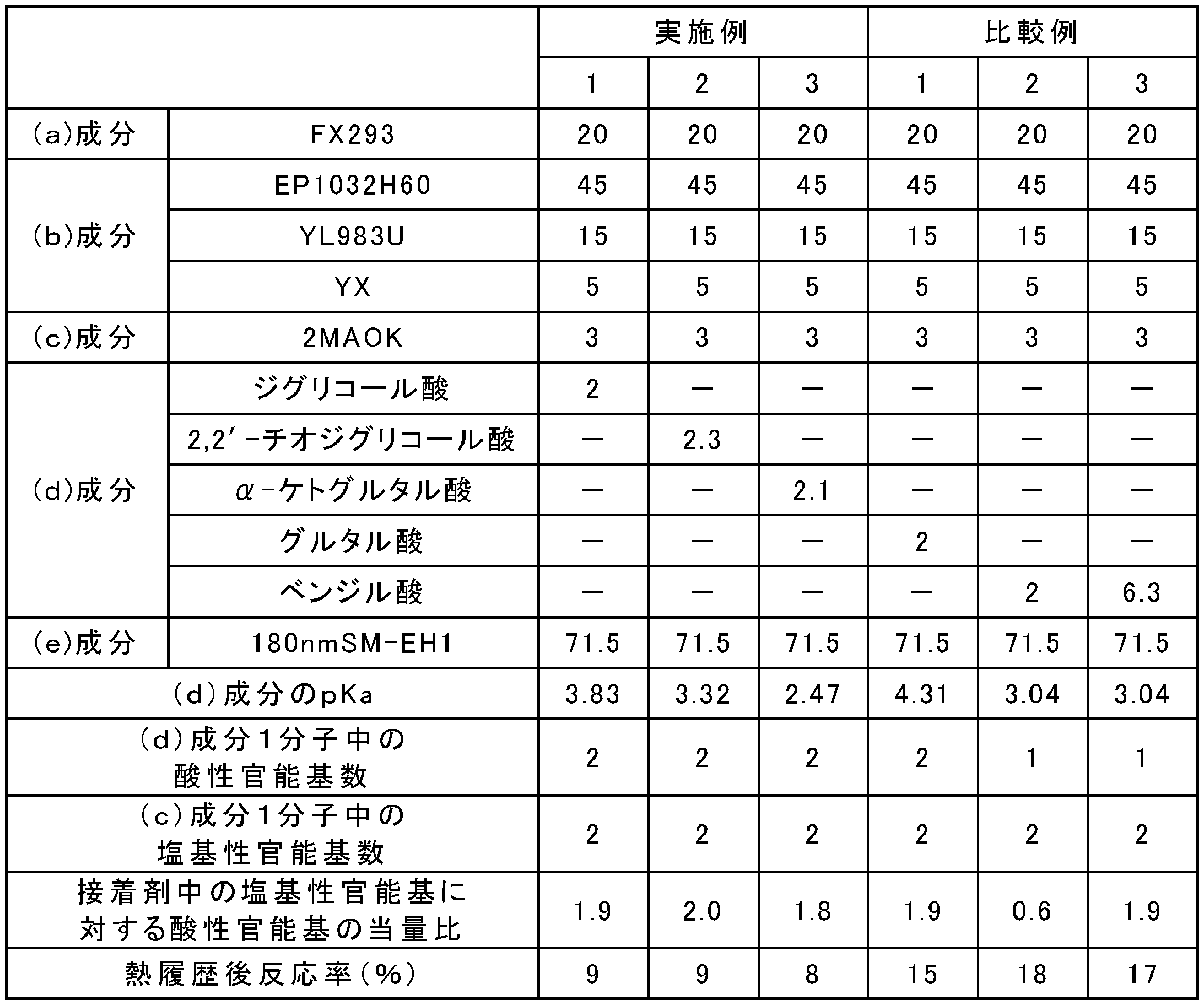

1…半導体チップ、2…基板、10…半導体チップ本体、15,16…配線又はバンプ、20…基板本体、30…はんだ、34…貫通電極、40…接着剤層、50…インターポーザー本体、100,300,500…半導体装置。
Claims (12)
- 熱可塑性樹脂、熱硬化性樹脂、硬化剤及び有機酸を含む半導体用接着剤であって、
前記有機酸は、酸性官能基を2個以上有する、酸解離定数pKaが4.0以下の化合物である、半導体用接着剤。 - 前記酸性官能基が、カルボキシル基、スルホキシル基及びリン酸基からなる群より選択される少なくとも一種の基を含む、請求項1に記載の半導体用接着剤。
- 前記硬化剤に含まれる塩基性官能基に対する、前記有機酸に含まれる前記酸性官能基の当量比が1.0以上である、請求項1又は2に記載の半導体用接着剤。
- 前記有機酸が、下記一般式(1-1)、(1-2)又は(1-3)で表される化合物を含む、請求項1~3のいずれか一項に記載の半導体用接着剤。



- 前記有機酸の融点が、50~250℃である、請求項1~4のいずれか一項に記載の半導体用接着剤。
- 前記硬化剤が、アミン系硬化剤を含む、請求項1~5のいずれか一項に記載の半導体用接着剤。
- 前記硬化剤が、イミダゾール系硬化剤を含む、請求項1~6のいずれか一項に記載の半導体用接着剤。
- 前記イミダゾール系硬化剤の構造が、トリアジン環を含む構造である、請求項7に記載の半導体用接着剤。
- 半導体チップ及び配線回路基板のそれぞれの接続部が互いに電気的に接続された半導体装置、又は、複数の半導体チップのそれぞれの接続部が互いに電気的に接続された半導体装置の製造方法であって、
請求項1~8のいずれか一項に記載の半導体用接着剤を、常圧又は加圧雰囲気下で熱を加えることにより硬化させ、硬化した前記半導体用接着剤により前記接続部の少なくとも一部を封止する封止工程を備える、半導体装置の製造方法。 - 前記封止工程の前に、
ステージ上に複数の半導体チップを配置する工程と、
前記ステージを60~155℃に加熱しながら、前記ステージ上に配置された前記複数の半導体チップのそれぞれの上に、前記半導体用接着剤を介して他の半導体チップを順次配置し、前記半導体チップ、前記半導体用接着剤及び前記他の半導体チップがこの順に積層されてなる積層体を複数得る仮固定工程と、を更に備える、請求項9に記載の半導体装置の製造方法。 - 前記封止工程の前に、
ステージ上に配線回路基板又は半導体ウェハを配置する工程と、
前記ステージを60~155℃に加熱しながら、前記ステージ上に配置された前記配線回路基板又は半導体ウェハの上に、前記半導体用接着剤を介して複数の半導体チップを順次配置し、前記配線回路基板、前記半導体用接着剤及び複数の前記半導体チップがこの順に積層されてなる積層体、又は、前記半導体ウェハ、前記半導体用接着剤及び複数の前記半導体チップがこの順に積層されてなる積層体を得る仮固定工程と、を更に備える、請求項9に記載の半導体装置の製造方法。 - 半導体チップ及び配線回路基板のそれぞれの接続部が互いに電気的に接続された半導体装置、又は、複数の半導体チップのそれぞれの接続部が互いに電気的に接続された半導体装置であって、前記接続部の少なくとも一部が、常圧又は加圧雰囲気下で熱を加えて硬化された請求項1~8のいずれか一項に記載の半導体用接着剤の硬化物によって封止されている、半導体装置。
Priority Applications (2)
| Application Number | Priority Date | Filing Date | Title |
|---|---|---|---|
| KR1020237008416A KR20230068394A (ko) | 2020-09-16 | 2021-09-13 | 반도체용 접착제, 및, 반도체 장치 및 그 제조 방법 |
| CN202180062120.2A CN116195052A (zh) | 2020-09-16 | 2021-09-13 | 半导体用黏合剂、以及半导体装置及其制造方法 |
Applications Claiming Priority (4)
| Application Number | Priority Date | Filing Date | Title |
|---|---|---|---|
| JP2020155498 | 2020-09-16 | ||
| JP2020-155498 | 2020-09-16 | ||
| JP2020-211410 | 2020-12-21 | ||
| JP2020211410A JP7647092B2 (ja) | 2020-09-16 | 2020-12-21 | 半導体用接着剤、並びに、半導体装置及びその製造方法 |
Publications (1)
| Publication Number | Publication Date |
|---|---|
| WO2022059640A1 true WO2022059640A1 (ja) | 2022-03-24 |
Family
ID=80777016
Family Applications (1)
| Application Number | Title | Priority Date | Filing Date |
|---|---|---|---|
| PCT/JP2021/033517 Ceased WO2022059640A1 (ja) | 2020-09-16 | 2021-09-13 | 半導体用接着剤、並びに、半導体装置及びその製造方法 |
Country Status (5)
| Country | Link |
|---|---|
| JP (2) | JP7647092B2 (ja) |
| KR (1) | KR20230068394A (ja) |
| CN (1) | CN116195052A (ja) |
| TW (1) | TWI895502B (ja) |
| WO (1) | WO2022059640A1 (ja) |
Families Citing this family (2)
| Publication number | Priority date | Publication date | Assignee | Title |
|---|---|---|---|---|
| CN116210081A (zh) * | 2020-09-16 | 2023-06-02 | 株式会社力森诺科 | 半导体用黏合剂、以及半导体装置及其制造方法 |
| JP2025005536A (ja) * | 2023-06-28 | 2025-01-17 | 株式会社レゾナック | 半導体装置を製造する方法 |
Citations (6)
| Publication number | Priority date | Publication date | Assignee | Title |
|---|---|---|---|---|
| JP2004179552A (ja) * | 2002-11-28 | 2004-06-24 | Nec Corp | 半導体装置の実装構造、実装方法およびリワーク方法 |
| WO2012053589A1 (ja) * | 2010-10-22 | 2012-04-26 | 日立化成工業株式会社 | 接着剤組成物、半導体装置の製造方法及び半導体装置 |
| WO2012153846A1 (ja) * | 2011-05-11 | 2012-11-15 | 日立化成工業株式会社 | 半導体装置の製造方法、半導体素子付き半導体ウェハの製造方法、接着剤層付き半導体ウェハの製造方法及び半導体ウェハ積層体の製造方法 |
| JP2014209624A (ja) * | 2014-04-18 | 2014-11-06 | パナソニック株式会社 | 回路基板と半導体部品との接合部構造 |
| WO2018235854A1 (ja) * | 2017-06-21 | 2018-12-27 | 日立化成株式会社 | 半導体用接着剤、半導体装置の製造方法及び半導体装置 |
| JP2019173023A (ja) * | 2019-06-03 | 2019-10-10 | 京セラ株式会社 | 半導体接着用シート及びそれを用いた半導体装置 |
Family Cites Families (10)
| Publication number | Priority date | Publication date | Assignee | Title |
|---|---|---|---|---|
| JP5217260B2 (ja) | 2007-04-27 | 2013-06-19 | 住友ベークライト株式会社 | 半導体ウエハーの接合方法および半導体装置の製造方法 |
| JP5703621B2 (ja) * | 2010-08-09 | 2015-04-22 | 日立化成株式会社 | 回路部材接続用接着剤、回路部材接続用接着剤シート、半導体装置及び半導体装置の製造方法 |
| JP2012089750A (ja) * | 2010-10-21 | 2012-05-10 | Hitachi Chem Co Ltd | 半導体封止充てん用熱硬化性樹脂組成物及び半導体装置 |
| JP5813479B2 (ja) * | 2011-11-28 | 2015-11-17 | 日東電工株式会社 | シート状封止組成物及び半導体装置の製造方法 |
| JP5867584B2 (ja) * | 2012-02-24 | 2016-02-24 | 日立化成株式会社 | 半導体用接着剤及び半導体装置の製造方法 |
| CN113214757A (zh) * | 2014-08-29 | 2021-08-06 | 古河电气工业株式会社 | 导电性接合剂组合物 |
| JP2015131969A (ja) * | 2015-04-06 | 2015-07-23 | 日立化成株式会社 | 半導体封止充てん用エポキシ樹脂組成物 |
| WO2017090439A1 (ja) * | 2015-11-24 | 2017-06-01 | リンテック株式会社 | 回路部材接続用樹脂シート |
| CN109314327B (zh) * | 2016-10-06 | 2022-04-05 | 积水化学工业株式会社 | 导电材料、连接结构体以及连接结构体的制造方法 |
| TWI784077B (zh) * | 2017-11-17 | 2022-11-21 | 日商迪愛生股份有限公司 | 環氧(甲基)丙烯酸酯樹脂組成物、硬化性樹脂組成物、硬化物及環氧(甲基)丙烯酸酯樹脂組成物之製造方法 |
-
2020
- 2020-12-21 JP JP2020211410A patent/JP7647092B2/ja active Active
-
2021
- 2021-09-13 KR KR1020237008416A patent/KR20230068394A/ko active Pending
- 2021-09-13 CN CN202180062120.2A patent/CN116195052A/zh active Pending
- 2021-09-13 WO PCT/JP2021/033517 patent/WO2022059640A1/ja not_active Ceased
- 2021-09-14 TW TW110134198A patent/TWI895502B/zh active
-
2025
- 2025-03-03 JP JP2025032646A patent/JP2025074222A/ja active Pending
Patent Citations (6)
| Publication number | Priority date | Publication date | Assignee | Title |
|---|---|---|---|---|
| JP2004179552A (ja) * | 2002-11-28 | 2004-06-24 | Nec Corp | 半導体装置の実装構造、実装方法およびリワーク方法 |
| WO2012053589A1 (ja) * | 2010-10-22 | 2012-04-26 | 日立化成工業株式会社 | 接着剤組成物、半導体装置の製造方法及び半導体装置 |
| WO2012153846A1 (ja) * | 2011-05-11 | 2012-11-15 | 日立化成工業株式会社 | 半導体装置の製造方法、半導体素子付き半導体ウェハの製造方法、接着剤層付き半導体ウェハの製造方法及び半導体ウェハ積層体の製造方法 |
| JP2014209624A (ja) * | 2014-04-18 | 2014-11-06 | パナソニック株式会社 | 回路基板と半導体部品との接合部構造 |
| WO2018235854A1 (ja) * | 2017-06-21 | 2018-12-27 | 日立化成株式会社 | 半導体用接着剤、半導体装置の製造方法及び半導体装置 |
| JP2019173023A (ja) * | 2019-06-03 | 2019-10-10 | 京セラ株式会社 | 半導体接着用シート及びそれを用いた半導体装置 |
Also Published As
| Publication number | Publication date |
|---|---|
| JP2022049640A (ja) | 2022-03-29 |
| KR20230068394A (ko) | 2023-05-17 |
| JP7647092B2 (ja) | 2025-03-18 |
| TW202223038A (zh) | 2022-06-16 |
| CN116195052A (zh) | 2023-05-30 |
| TWI895502B (zh) | 2025-09-01 |
| JP2025074222A (ja) | 2025-05-13 |
Similar Documents
| Publication | Publication Date | Title |
|---|---|---|
| JP5900602B2 (ja) | 半導体用接着剤、フラックス剤、半導体装置の製造方法及び半導体装置 | |
| JP5958529B2 (ja) | 半導体装置及びその製造方法 | |
| JP7726356B2 (ja) | 半導体用接着剤 | |
| TWI818911B (zh) | 半導體用接著劑、半導體裝置的製造方法及半導體裝置 | |
| JP2025074222A (ja) | 半導体用接着剤、並びに、半導体装置及びその製造方法 | |
| TW202219220A (zh) | 半導體用接著劑、以及半導體裝置及其製造方法 | |
| JPWO2020110785A1 (ja) | 半導体用フィルム状接着剤、半導体装置及びその製造方法 | |
| JP7172167B2 (ja) | 半導体装置の製造方法、及びそれに用いられる半導体用接着剤 | |
| JP7732460B2 (ja) | 半導体用接着剤、並びに、半導体装置及びその製造方法 | |
| WO2022024648A1 (ja) | 半導体装置を製造する方法、及びフィルム状接着剤 | |
| WO2024053232A1 (ja) | 積層フィルム及び半導体装置の製造方法 | |
| JP2020136398A (ja) | 半導体用接着剤 |
Legal Events
| Date | Code | Title | Description |
|---|---|---|---|
| 121 | Ep: the epo has been informed by wipo that ep was designated in this application |
Ref document number: 21869327 Country of ref document: EP Kind code of ref document: A1 |
|
| NENP | Non-entry into the national phase |
Ref country code: DE |
|
| 122 | Ep: pct application non-entry in european phase |
Ref document number: 21869327 Country of ref document: EP Kind code of ref document: A1 |