WO2022054853A1 - 薬液耐性保護膜 - Google Patents
薬液耐性保護膜 Download PDFInfo
- Publication number
- WO2022054853A1 WO2022054853A1 PCT/JP2021/033084 JP2021033084W WO2022054853A1 WO 2022054853 A1 WO2022054853 A1 WO 2022054853A1 JP 2021033084 W JP2021033084 W JP 2021033084W WO 2022054853 A1 WO2022054853 A1 WO 2022054853A1
- Authority
- WO
- WIPO (PCT)
- Prior art keywords
- group
- protective film
- carbon atoms
- forming composition
- substituted
- Prior art date
- Legal status (The legal status is an assumption and is not a legal conclusion. Google has not performed a legal analysis and makes no representation as to the accuracy of the status listed.)
- Ceased
Links
- BRPSWMCDEYMRPE-UHFFFAOYSA-N CC(c(cc1)ccc1O)(c(cc1)ccc1O)c(cc1)ccc1O Chemical compound CC(c(cc1)ccc1O)(c(cc1)ccc1O)c(cc1)ccc1O BRPSWMCDEYMRPE-UHFFFAOYSA-N 0.000 description 1
Classifications
-
- G—PHYSICS
- G03—PHOTOGRAPHY; CINEMATOGRAPHY; ANALOGOUS TECHNIQUES USING WAVES OTHER THAN OPTICAL WAVES; ELECTROGRAPHY; HOLOGRAPHY
- G03F—PHOTOMECHANICAL PRODUCTION OF TEXTURED OR PATTERNED SURFACES, e.g. FOR PRINTING, FOR PROCESSING OF SEMICONDUCTOR DEVICES; MATERIALS THEREFOR; ORIGINALS THEREFOR; APPARATUS SPECIALLY ADAPTED THEREFOR
- G03F7/00—Photomechanical, e.g. photolithographic, production of textured or patterned surfaces, e.g. printing surfaces; Materials therefor, e.g. comprising photoresists; Apparatus specially adapted therefor
- G03F7/004—Photosensitive materials
- G03F7/038—Macromolecular compounds which are rendered insoluble or differentially wettable
- G03F7/0385—Macromolecular compounds which are rendered insoluble or differentially wettable using epoxidised novolak resin
-
- C—CHEMISTRY; METALLURGY
- C08—ORGANIC MACROMOLECULAR COMPOUNDS; THEIR PREPARATION OR CHEMICAL WORKING-UP; COMPOSITIONS BASED THEREON
- C08G—MACROMOLECULAR COMPOUNDS OBTAINED OTHERWISE THAN BY REACTIONS ONLY INVOLVING UNSATURATED CARBON-TO-CARBON BONDS
- C08G59/00—Polycondensates containing more than one epoxy group per molecule; Macromolecules obtained by polymerising compounds containing more than one epoxy group per molecule using curing agents or catalysts which react with the epoxy groups
- C08G59/18—Macromolecules obtained by polymerising compounds containing more than one epoxy group per molecule using curing agents or catalysts which react with the epoxy groups ; e.g. general methods of curing
- C08G59/40—Macromolecules obtained by polymerising compounds containing more than one epoxy group per molecule using curing agents or catalysts which react with the epoxy groups ; e.g. general methods of curing characterised by the curing agents used
- C08G59/62—Alcohols or phenols
- C08G59/621—Phenols
-
- C—CHEMISTRY; METALLURGY
- C08—ORGANIC MACROMOLECULAR COMPOUNDS; THEIR PREPARATION OR CHEMICAL WORKING-UP; COMPOSITIONS BASED THEREON
- C08G—MACROMOLECULAR COMPOUNDS OBTAINED OTHERWISE THAN BY REACTIONS ONLY INVOLVING UNSATURATED CARBON-TO-CARBON BONDS
- C08G59/00—Polycondensates containing more than one epoxy group per molecule; Macromolecules obtained by polymerising compounds containing more than one epoxy group per molecule using curing agents or catalysts which react with the epoxy groups
- C08G59/18—Macromolecules obtained by polymerising compounds containing more than one epoxy group per molecule using curing agents or catalysts which react with the epoxy groups ; e.g. general methods of curing
- C08G59/40—Macromolecules obtained by polymerising compounds containing more than one epoxy group per molecule using curing agents or catalysts which react with the epoxy groups ; e.g. general methods of curing characterised by the curing agents used
-
- C—CHEMISTRY; METALLURGY
- C09—DYES; PAINTS; POLISHES; NATURAL RESINS; ADHESIVES; COMPOSITIONS NOT OTHERWISE PROVIDED FOR; APPLICATIONS OF MATERIALS NOT OTHERWISE PROVIDED FOR
- C09D—COATING COMPOSITIONS, e.g. PAINTS, VARNISHES OR LACQUERS; FILLING PASTES; CHEMICAL PAINT OR INK REMOVERS; INKS; CORRECTING FLUIDS; WOODSTAINS; PASTES OR SOLIDS FOR COLOURING OR PRINTING; USE OF MATERIALS THEREFOR
- C09D163/00—Coating compositions based on epoxy resins; Coating compositions based on derivatives of epoxy resins
- C09D163/04—Epoxynovolacs
-
- G—PHYSICS
- G03—PHOTOGRAPHY; CINEMATOGRAPHY; ANALOGOUS TECHNIQUES USING WAVES OTHER THAN OPTICAL WAVES; ELECTROGRAPHY; HOLOGRAPHY
- G03F—PHOTOMECHANICAL PRODUCTION OF TEXTURED OR PATTERNED SURFACES, e.g. FOR PRINTING, FOR PROCESSING OF SEMICONDUCTOR DEVICES; MATERIALS THEREFOR; ORIGINALS THEREFOR; APPARATUS SPECIALLY ADAPTED THEREFOR
- G03F7/00—Photomechanical, e.g. photolithographic, production of textured or patterned surfaces, e.g. printing surfaces; Materials therefor, e.g. comprising photoresists; Apparatus specially adapted therefor
- G03F7/004—Photosensitive materials
- G03F7/0045—Photosensitive materials with organic non-macromolecular light-sensitive compounds not otherwise provided for, e.g. dissolution inhibitors
-
- G—PHYSICS
- G03—PHOTOGRAPHY; CINEMATOGRAPHY; ANALOGOUS TECHNIQUES USING WAVES OTHER THAN OPTICAL WAVES; ELECTROGRAPHY; HOLOGRAPHY
- G03F—PHOTOMECHANICAL PRODUCTION OF TEXTURED OR PATTERNED SURFACES, e.g. FOR PRINTING, FOR PROCESSING OF SEMICONDUCTOR DEVICES; MATERIALS THEREFOR; ORIGINALS THEREFOR; APPARATUS SPECIALLY ADAPTED THEREFOR
- G03F7/00—Photomechanical, e.g. photolithographic, production of textured or patterned surfaces, e.g. printing surfaces; Materials therefor, e.g. comprising photoresists; Apparatus specially adapted therefor
- G03F7/004—Photosensitive materials
- G03F7/09—Photosensitive materials characterised by structural details, e.g. supports, auxiliary layers
- G03F7/11—Photosensitive materials characterised by structural details, e.g. supports, auxiliary layers having cover layers or intermediate layers, e.g. subbing layers
-
- G—PHYSICS
- G03—PHOTOGRAPHY; CINEMATOGRAPHY; ANALOGOUS TECHNIQUES USING WAVES OTHER THAN OPTICAL WAVES; ELECTROGRAPHY; HOLOGRAPHY
- G03F—PHOTOMECHANICAL PRODUCTION OF TEXTURED OR PATTERNED SURFACES, e.g. FOR PRINTING, FOR PROCESSING OF SEMICONDUCTOR DEVICES; MATERIALS THEREFOR; ORIGINALS THEREFOR; APPARATUS SPECIALLY ADAPTED THEREFOR
- G03F7/00—Photomechanical, e.g. photolithographic, production of textured or patterned surfaces, e.g. printing surfaces; Materials therefor, e.g. comprising photoresists; Apparatus specially adapted therefor
- G03F7/16—Coating processes; Apparatus therefor
- G03F7/168—Finishing the coated layer, e.g. drying, baking, soaking
-
- G—PHYSICS
- G03—PHOTOGRAPHY; CINEMATOGRAPHY; ANALOGOUS TECHNIQUES USING WAVES OTHER THAN OPTICAL WAVES; ELECTROGRAPHY; HOLOGRAPHY
- G03F—PHOTOMECHANICAL PRODUCTION OF TEXTURED OR PATTERNED SURFACES, e.g. FOR PRINTING, FOR PROCESSING OF SEMICONDUCTOR DEVICES; MATERIALS THEREFOR; ORIGINALS THEREFOR; APPARATUS SPECIALLY ADAPTED THEREFOR
- G03F7/00—Photomechanical, e.g. photolithographic, production of textured or patterned surfaces, e.g. printing surfaces; Materials therefor, e.g. comprising photoresists; Apparatus specially adapted therefor
- G03F7/20—Exposure; Apparatus therefor
-
- G—PHYSICS
- G03—PHOTOGRAPHY; CINEMATOGRAPHY; ANALOGOUS TECHNIQUES USING WAVES OTHER THAN OPTICAL WAVES; ELECTROGRAPHY; HOLOGRAPHY
- G03F—PHOTOMECHANICAL PRODUCTION OF TEXTURED OR PATTERNED SURFACES, e.g. FOR PRINTING, FOR PROCESSING OF SEMICONDUCTOR DEVICES; MATERIALS THEREFOR; ORIGINALS THEREFOR; APPARATUS SPECIALLY ADAPTED THEREFOR
- G03F7/00—Photomechanical, e.g. photolithographic, production of textured or patterned surfaces, e.g. printing surfaces; Materials therefor, e.g. comprising photoresists; Apparatus specially adapted therefor
- G03F7/20—Exposure; Apparatus therefor
- G03F7/2002—Exposure; Apparatus therefor with visible light or UV light, through an original having an opaque pattern on a transparent support, e.g. film printing, projection printing; by reflection of visible or UV light from an original such as a printed image
- G03F7/2014—Contact or film exposure of light sensitive plates such as lithographic plates or circuit boards, e.g. in a vacuum frame
- G03F7/2016—Contact mask being integral part of the photosensitive element and subject to destructive removal during post-exposure processing
-
- G—PHYSICS
- G03—PHOTOGRAPHY; CINEMATOGRAPHY; ANALOGOUS TECHNIQUES USING WAVES OTHER THAN OPTICAL WAVES; ELECTROGRAPHY; HOLOGRAPHY
- G03F—PHOTOMECHANICAL PRODUCTION OF TEXTURED OR PATTERNED SURFACES, e.g. FOR PRINTING, FOR PROCESSING OF SEMICONDUCTOR DEVICES; MATERIALS THEREFOR; ORIGINALS THEREFOR; APPARATUS SPECIALLY ADAPTED THEREFOR
- G03F7/00—Photomechanical, e.g. photolithographic, production of textured or patterned surfaces, e.g. printing surfaces; Materials therefor, e.g. comprising photoresists; Apparatus specially adapted therefor
- G03F7/26—Processing photosensitive materials; Apparatus therefor
-
- H—ELECTRICITY
- H10—SEMICONDUCTOR DEVICES; ELECTRIC SOLID-STATE DEVICES NOT OTHERWISE PROVIDED FOR
- H10P—GENERIC PROCESSES OR APPARATUS FOR THE MANUFACTURE OR TREATMENT OF DEVICES COVERED BY CLASS H10
- H10P14/00—Formation of materials, e.g. in the shape of layers or pillars
- H10P14/60—Formation of materials, e.g. in the shape of layers or pillars of insulating materials
-
- H—ELECTRICITY
- H10—SEMICONDUCTOR DEVICES; ELECTRIC SOLID-STATE DEVICES NOT OTHERWISE PROVIDED FOR
- H10P—GENERIC PROCESSES OR APPARATUS FOR THE MANUFACTURE OR TREATMENT OF DEVICES COVERED BY CLASS H10
- H10P95/00—Generic processes or apparatus for manufacture or treatments not covered by the other groups of this subclass
- H10P95/08—Planarisation of organic insulating materials
Definitions
- the present invention relates to a composition for forming a protective film having excellent resistance to a wet etching solution for semiconductors in a lithography process in semiconductor manufacturing.
- the present invention also relates to a protective film formed from the composition, a method for manufacturing a substrate with a resist pattern to which the protective film is applied, and a method for manufacturing a semiconductor device.
- Patent Document 1 discloses a resist underlayer film material having resistance to alkaline hydrogen peroxide solution.
- the protective film When a protective film for a semiconductor substrate is formed using the protective film forming composition and the underlying substrate is processed by wet etching using the protective film as an etching mask, the protective film has a good mask function for a wet etching solution for semiconductors (that is,). , The masked part can protect the substrate).
- the protective film used for the above purpose is expected to have a function as a resist underlayer film for solving problems (shape defects, etc.) during so-called resist pattern formation.
- An object of the present invention is to solve the above problems.
- the present invention includes the following.
- n1 represents an integer of 0 to 3
- L 1 Represents a single bond or an alkylene group having 1 to 10 carbon atoms
- E represents an epoxy group
- B A compound or polymer having a phenolic hydroxy group other than catechol
- C Thermal acid generator
- D solvent
- a protective film forming composition for a wet etching solution for semiconductors which comprises.
- R 2 and T 2 are independently each of a halogeno group, a carboxy group, a nitro group, a cyano group, a methylenedioxy group, an acetoxy group, a methylthio group, an alkoxy group having 1 to 9 carbon atoms, and a carbon atom. It represents an alkyl group having 1 to 10 carbon atoms which may be substituted with an amino group which may be substituted with an alkyl group of the number 1 to 3, a hydroxy group or a halogeno group.
- a 1 and A 2 are independent of each other.
- a represents an integer of 1 to 6.
- n3 to n5 each independently represent an integer of 0 to 2.
- r2 represents an integer from 0 to 3.
- Each of m1 and m2 independently represents a number from 0 to 10,000,000. )
- Q 1 is a single bond, an oxygen atom, a sulfur atom, a sulfonyl group and a carbonyl group.
- A represents an integer of 1 to 6.
- n6 represents 0 to 2.
- R3 represents an integer of 0 to 3.
- n7 represents an integer of 0 to 2.
- a represents an integer of 1 to 6.
- a protective film against a wet etching solution for semiconductors which is a fired product of a coating film comprising the protective film forming composition according to any one of [1] to [6].
- n1 represents an integer of 0 to 3
- L 1 Represents a single bond or an alkylene group having 1 to 10 carbon atoms
- E represents an epoxy group
- B A compound or polymer having a phenolic hydroxy group other than catechol
- C Thermal acid generator
- D solvent
- a resist underlayer film forming composition comprising.
- a resist underlayer film characterized by being a fired product of a coating film comprising the resist underlayer film forming composition according to [8].
- a semiconductor which comprises a step of applying the protective film forming composition according to any one of [1] to [6] onto a semiconductor substrate having a step and firing to form the protective film.
- a method for manufacturing a substrate with a protective film which is characterized by being used.
- the protective film composition according to any one of [1] to [6] or the resist underlayer film forming composition according to [8] is applied onto a semiconductor substrate and fired to obtain a resist underlayer film.
- a method for manufacturing a substrate with a resist pattern which comprises a step of forming a protective film, a step of forming a resist film on the protective film, and then exposure and development to form a resist pattern, which is used for manufacturing a semiconductor. ..
- a protective film is formed on a semiconductor substrate on which an inorganic film may be formed on the surface using the protective film forming composition according to any one of [1] to [6], and the protective film is formed.
- a resist pattern is formed on the film, the protective film is dry-etched using the resist pattern as a mask, the surface of the inorganic film or the semiconductor substrate is exposed, and the protective film after dry etching is used as a mask for semiconductor wet.
- a method for manufacturing a semiconductor device which comprises a step of wet etching and cleaning the inorganic film or the semiconductor substrate using an etching solution.
- a resist underlayer film is formed using the resist underlayer film forming composition according to [8] on a semiconductor substrate on which an inorganic film may be formed on the surface, and a resist pattern is formed on the resist underlayer film.
- the resist underlayer film is formed and dry-etched using the resist pattern as a mask to expose the surface of the inorganic film or the semiconductor substrate, and the resist underlayer film after dry etching is used as a mask to dry-etch the inorganic film or the semiconductor substrate.
- a method for manufacturing a semiconductor device including a step of etching a resist.
- the protective film forming composition of the present invention is required to have, for example, the following characteristics in a well-balanced manner in the lithography process in semiconductor manufacturing. (1) It has a good masking function against wet etching liquid when processing a base substrate, (2) It reduces damage to the protective film or resist underlayer film when processing a substrate due to a low dry etching rate, and (3) Steps. Excellent flatness of the substrate, (4) Excellent embedding property in the fine trench pattern substrate, and having the performances of (1) to (4) in a well-balanced manner facilitates fine processing of the semiconductor substrate. It can be carried out.
- the protective film forming composition for a wet etching solution for semiconductors of the present invention is used.
- A Polymer having a unit structure represented by the following formula (1-1):
- Ar represents a benzene ring, a naphthalene ring or an anthracene ring
- R 1 is a hydroxy group, a mercapto group which may be protected by a methyl group, or an amino which may be protected by a methyl group.
- n1 represents an integer of 0 to 3
- L 1 Represents a single bond or an alkylene group having 1 to 10 carbon atoms
- E represents an epoxy group
- B A compound or polymer having a phenolic hydroxy group other than catechol
- C Thermal acid generator
- D solvent, including.
- the polymer (A) used in the present invention is a polymer having a unit structure represented by the following formula (1-1): (In formula (1-1), Ar represents a benzene ring, a naphthalene ring or an anthracene ring, and R 1 is protected by a hydroxy group or a methyl group as a substituent of a hydrogen atom contained in the benzene ring, a naphthalene ring or an anthracene ring.
- the number of carbon atoms may be 1 to 10 which may be substituted with a mercapto group, an amino group which may be protected with a methyl group, a halogeno group, or may be substituted with a hetero atom or substituted with a hydroxy group.
- N1 represents an integer of 0 to 3
- L 1 represents a single bond or an alkylene group having 1 to 10 carbon atoms
- E represents an epoxy group
- alkyl group having 1 to 10 carbon atoms examples include a methyl group, an ethyl group, an n-propyl group, an i-propyl group, a cyclopropyl group, an n-butyl group, an i-butyl group, an s-butyl group, and t-.
- alkylene group having 1 to 10 carbon atoms examples include a methylene group, an ethylene group, an n-propylene group, an isopropylene group, a cyclopropylene group, an n-butylene group, an isobutylene group, an s-butylene group and a t-butylene group.
- Cyclobutylene group 1-methyl-cyclopropylene group, 2-methyl-cyclopropylene group, n-pentylene group, 1-methyl-n-butylene group, 2-methyl-n-butylene group, 3-methyl-n-butylene Group, 1,1-dimethyl-n-propylene group, 1,2-dimethyl-n-propylene group, 2,2-dimethyl-n-propylene, 1-ethyl-n-propylene group, cyclopentylene group, 1- Methyl-cyclobutylene group, 2-methyl-cyclobutylene group, 3-methyl-cyclobutylene group, 1,2-dimethyl-cyclopropylene group, 2,3-dimethyl-cyclopropylene group, 1-ethyl-cyclopropylene group, 2-Ethyl-cyclopropylene group, n-hexylene group, 1-methyl-n-pentylene group, 2-methyl-n-pentylene group, 3-methyl-n-pentylene group, 4-
- the R 1 may be an alkoxy group having 1 to 10 carbon atoms.
- alkoxy group having 1 to 10 carbon atoms examples include a methoxy group, an ethoxy group, an n-propoxy group, an i-propoxy group, an n-butoxy group, an i-butoxy group, an s-butoxy group, a t-butoxy group and an n-.
- Pentoxy group 1-methyl-n-butoxy group, 2-methyl-n-butoxy group, 3-methyl-n-butoxy group, 1,1-dimethyl-n-propoxy group, 1,2-dimethyl-n-propoxy Group, 2,2-dimethyl-n-propoxy group, 1-ethyl-n-propoxy group, n-hexyloxy group, 1-methyl-n-pentyloxy group, 2-methyl-n-pentyloxy group, 3- Methyl-n-pentyloxy group, 4-methyl-n-pentyloxy group, 1,1-dimethyl-n-butoxy group, 1,2-dimethyl-n-butoxy group, 1,3-dimethyl-n-butoxy group , 2,2-Dimethyl-n-butoxy group, 2,3-dimethyl-n-butoxy group, 3,3-dimethyl-n-butoxy group, 1-ethyl-n-butoxy group, 2-ethyl-n-butoxy group Group, 1,1,2-trimethyl-n-propoxy group
- the unit structure represented by the above formula (1-1) may be one type or a combination of two or more types.
- a copolymer having a plurality of unit structures in which Ar is the same type may be used, and the types of Ar are different, for example, Ar has a unit structure containing a benzene ring and a unit structure having a naphthalene ring.
- Copolymers having a plurality of unit structures are not excluded from the technical scope of the present application.
- any carbon-carbon atom in the alkylene group is a heteroatom (that is, in the case of oxygen, an ether bond or sulfur).
- it means that it is interrupted by a sulfide bond), an ester bond, or an amide bond. Bond, sulfide bond in the case of sulfur), ester bond or amide bond.
- the T 1 represents an alkylene group having 1 to 10 carbon atoms which may be interrupted by a single bond or an ether bond, an ester bond or an amide bond, and is a combination of an ether bond and a methylene group. (That is, when " -T1-1- (E) n2" in the formula (1-1) is a glycidyl ether group), a combination of an ester bond and a methylene group, or a combination of an amide bond and a methylene group is preferable. ..
- the alkyl group having 1 to 10 carbon atoms which may be substituted with a hetero atom is a hetero atom (preferably a halogeno group) in which one or more hydrogen atoms of the alkyl group having 1 to 10 carbon atoms have. It means that it has been replaced.
- the L 1 represents a single bond or an alkylene group having 1 to 10 carbon atoms, and the following formula (1-2):
- R 2 and R 3 are independent of each other and have a hydrogen atom, a methyl group, an ethyl group, an n-propyl group, an i-propyl group, a cyclopropyl group, an n-butyl group, and i-. It represents a butyl group, an s-butyl group, a t-butyl group, and a cyclobutyl group, and R 2 and R 3 may be bonded to each other to form a ring having 3 to 6 carbon atoms). .. Among these, it is preferable that both R 2 and R 3 are hydrogen atoms (that is,-(CR 2 R 3 )-is a methylene group).
- the halogeno group refers to halogen-X (F, Cl, Br, I) substituted with hydrogen.
- the polymer (A) is not particularly limited as long as it satisfies the unit structure of the formula (1-1). It may be manufactured by a method known per se. Commercially available products may be used. Commercially available products include the heat-resistant epoxy novolak resin EOCN (registered trademark) series (manufactured by Nippon Kayaku Co., Ltd., epoxy novolak resin DEN (registered trademark) series (manufactured by Dow Chemical Japan Co., Ltd.), etc. Can be mentioned.
- EOCN registered trademark
- DEN registered trademark
- the weight average molecular weight of the polymer (A) is 100 or more, 500 to 200,000, 600 to 50,000, or 700 to 10,000.
- Examples of the polymer (A) of the present application include those having the following unit structure.
- the compound or polymer (B) having a phenolic hydroxy group other than the catechol is not particularly limited as long as it is a compound or polymer that does not impair the effects of the present invention. Needless to say, the compound or polymer (B) having a phenolic hydroxy group other than the catechol is different from the polymer (A).
- the weight average molecular weight of the compound or polymer (B) having a phenolic hydroxy group other than the catechol is not particularly limited, but is, for example, 300 to 50,000.
- the compound (B) or the polymer has two or more phenolic hydroxy groups.
- R 2 and T 2 are independently each of a halogeno group, a carboxy group, a nitro group, a cyano group, a methylenedioxy group, an acetoxy group, a methylthio group, an alkoxy group having 1 to 9 carbon atoms, and a carbon atom.
- R 2 and T 2 are independently each of a halogeno group, a carboxy group, a nitro group, a cyano group, a methylenedioxy group, an acetoxy group, a methylthio group, an alkoxy group having 1 to 9 carbon atoms, and a carbon atom.
- R 2 and T 2 are independently each of a halogeno group, a carboxy group, a nitro group, a cyano group, a methylenedioxy group, an acetoxy group, a methylthio group, an alkoxy group having 1 to 9 carbon atoms, and a carbon atom.
- In (formula 2-1a) represents a bonding site with a carbon atom to which T 3 is bonded.
- a represents an integer of 1 to 6.
- n3 to n5 each independently represents an integer of 0 to 2.
- r2 represents an integer of 0 to 3.
- m1 and m2 each independently represent 0 to 10,000,000. Represents.
- bicyclocyclic compound examples include dicyclopentadiene, substituted dicyclopentadiene, tetracyclo [4.4.0.12,5.17,10] dodeca-3,8-diene, or substituted tetracyclo [4.4.0. 12,5.17,10] Dodeca-3,8-diene.
- substitution means that one or more hydrogen atoms of the bicyclo ring compound may be independently substituted with a halogeno group, a nitro group, an amino group or a hydroxy group or a group thereof, and the number of carbon atoms may be 1. It means that it is substituted with an alkyl group of about 10 or an aryl group having 6 to 40 carbon atoms.
- the divalent organic group derived from the bicyclo ring compound is a group having two bonds derived by removing any two hydrogen atoms from the bicyclo ring compound.
- Examples of the aryl group having 6 to 40 carbon atoms include a phenyl group, an o-methylphenyl group, an m-methylphenyl group, a p-methylphenyl group, an o-chlorphenyl group, an m-chlorphenyl group and a p-chlorphenyl group.
- the compound having a phenolic hydroxy group other than the above (B) catechol may be a compound shown below.
- the compound (B) is a compound having a phenolic hydroxy group other than (B) catechol, and is particularly limited as long as it is a compound that does not impair the effects of the present invention.
- the compound (B) is represented by the following formula (2-2): (In the formula, R 3 is a halogeno group, a carboxy group, a nitro group, a cyano group, a methylenedioxy group, an acetoxy group, a methylthio group, an alkoxy group having 1 to 9 carbon atoms, and an alkyl group having 1 to 3 carbon atoms.
- It represents an alkyl group having 1 to 10 carbon atoms which may be substituted with an amino group, a hydroxy group or a halogeno group which may be substituted.
- Q 1 is a single bond, an oxygen atom, a sulfur atom, a sulfonyl group and a carbonyl group.
- A represents an integer of 1 to 6.
- n6 represents 0 to 2.
- R3 represents an integer of 0 to 3.
- Examples of the arylene group having 6 to 40 carbon atoms include a phenylene group, an o-methylphenylene group, an m-methylphenylene group, a p-methylphenylene group, an o-chlorphenylene group, an m-chlorphenylene group and a p-chlorphenylene group.
- the group is mentioned.
- alkylene group having 1 to 10 carbon atoms examples include a methylene group, an ethylene group, an n-propylene group, an isopropylene group, a cyclopropylene group, an n-butylene group, an isobutylene group, an s-butylene group, a t-butylene group and a cyclo.
- the compound (B) may be represented by the following formula (4-1):
- R5 is a halogeno group, a carboxy group, a nitro group, a cyano group, a methylenedioxy group, an acetoxy group, a methylthio group, an alkoxy group having 1 to 9 carbon atoms, and an alkyl group having 1 to 3 carbon atoms. It represents an alkyl group having 1 to 10 carbon atoms which may be substituted with an amino group, a hydroxy group or a halogeno group which may be substituted.
- n8 represents an integer of 4, 5, 6 or 8.
- the compound (B) may be of the following formula (5-1) and formula (5-1-a):
- n9 and n10 represent integers of 0 or 1 , respectively, and R6 is a halogeno group, a carboxy group, a nitro group, a cyano group, a methylenedioxy group, an acetoxy group, a methylthio group, and 1 to 9 carbon atoms. It represents an alkoxy group, an amino group optionally substituted with an alkyl group having 1 to 3 carbon atoms, an alkyl group optionally substituted with a hydroxy group or a halogeno group, and an alkyl group having 1 to 10 carbon atoms.
- n11 represents an integer of 1 or 2.
- r5 represents an integer of 0 to 3.
- * represents a compound of formula (5-1) and a compound of formula (5-1-a). Represents the binding site of.
- the compound having a phenolic hydroxy group other than (B) catechol may be a compound shown below.
- the compound or polymer (B) having a phenolic hydroxy group other than catechol shall be the polymer (B) having a phenolic hydroxy group other than catechol.
- the present invention is not particularly limited as long as it is a polymer capable of producing the same and does not impair the effects of the present invention.
- the polymer (B) preferably has at least 3 or more repeating unit structures.
- the weight average molecular weight of the polymer (B) is not particularly limited, but is, for example, 1,000 to 50,000.
- the polymer (B) contains a unit structure represented by the following formula (3-1):
- T 4 represents an alkyl group having 1 to 10 carbon atoms which may be substituted with a halogeno group.
- R 4 is a halogeno group, a carboxy group, a nitro group, a cyano group, a methylenedioxy group and an acetoxy group.
- r4 represents an integer of 0 to 3.
- n7 represents an integer of 0 to 2.
- a represents an integer of 1 to 6.
- the description of the halogeno group, the alkyl group and the alkoxy group is as described above.
- the polymer represented by the formula (3-1) may be a polymer containing one type of unit structure represented by the formula (3-1) or a copolymer containing two or more types.
- polymer (B) represented by the above formula (3-1) include a polymer containing the unit structure described below.
- the protective film-forming composition of the present application may further contain a thermoacid generator.
- thermoacid generator examples include pyridinium-p-toluenesulfonate, pyridinium-trifluoromethanesulfonate, pyrinidium-p-phenolsulfonate, K-PURE® CXC-1612, CXC-1614, and TAG. -2172, TAG-2179, TAG-2678, TAG2689 (above, King Industries), and SI-45, SI-60, SI-80, SI-100, SI-110, SI-150 (above). , Manufactured by Sanshin Chemical Industry Co., Ltd.).
- thermal acid generators can be used alone or in combination of two or more.
- the protective film-forming composition of the present application contains a thermoacid generator
- the content thereof is 0.0001 to 20% by mass, preferably 0.01 to 15% by mass, based on the total solid content of the protective film-forming composition. %, More preferably 0.1 to 10% by mass.
- the protective film-forming composition of the present invention can be prepared by dissolving each of the above components in a solvent, preferably an organic solvent, and is used in a uniform solution state.
- the organic solvent of the protective film forming composition according to the present invention can be used without particular limitation as long as it is an organic solvent capable of dissolving the above compound or a solid component such as the acid catalyst described below.
- the protective film forming composition according to the present invention is used in a uniform solution state, it is recommended to use an organic solvent generally used in the lithography process in combination in consideration of its coating performance. ..
- organic solvent examples include ethylene glycol monomethyl ether, ethylene glycol monoethyl ether, methyl cellosolve acetate, ethyl cellosolve acetate, diethylene glycol monomethyl ether, diethylene glycol monoethyl ether, propylene glycol, propylene glycol monomethyl ether, and propylene glycol monoethyl ether.
- propylene glycol monomethyl ether propylene glycol monomethyl ether acetate, ethyl lactate, butyl lactate, cyclohexanone and the like are preferable.
- propylene glycol monomethyl ether and propylene glycol monomethyl ether acetate are preferable.
- the solid content of the protective film forming composition according to the present invention is usually 0.1 to 70% by mass, preferably 0.1 to 60% by mass.
- the solid content is the content ratio of all the components excluding the solvent from the protective film forming composition.
- the proportion of the polymer represented by the above formula (1-1) in the solid content is 1 to 100% by mass, 1 to 99.9% by mass, 50 to 99.9% by mass, 50 to 95% by mass, 50. It is preferable in the order of ⁇ 90% by mass.
- the resist underlayer film forming composition of the present invention is (A) a polymer having a unit structure represented by the following formula (1-1): (In the formula (1-1), Ar represents a benzene ring, a naphthalene ring or an anthracene ring, and R 1 is a hydroxy group, a mercapto group which may be protected by a methyl group, or an amino which may be protected by a methyl group.
- n1 represents an integer of 0 to 3
- L 1 Represents a single bond or an alkylene group having 1 to 10 carbon atoms
- E represents an epoxy group
- the substrate with a resist pattern according to the present invention can be produced by applying the above-mentioned protective film forming composition (resist underlayer film forming composition) onto a semiconductor substrate and firing it.
- protective film forming composition resist underlayer film forming composition
- Examples of the semiconductor substrate to which the protective film forming composition (resist underlayer film forming composition) of the present invention is applied include silicon wafers, germanium wafers, and gallium arsenide, indium arsenide, gallium nitride, indium nitride, and aluminum nitride. Examples thereof include compound semiconductor wafers such as.
- the inorganic film can be, for example, ALD (atomic layer deposition) method, CVD (chemical vapor deposition) method, reactive sputtering method, ion plating method, vacuum deposition. It is formed by a method, a spin coating method (spin-on-glass: SOG).
- the inorganic film examples include a polysilicon film, a silicon oxide film, a silicon nitride film, a silicon nitride film, a BPSG (Boro-Phospho Silicone Glass) film, a titanium nitride film, a titanium oxynitride film, a tungsten nitride film, and a gallium nitride film. , And a gallium hydride film.
- the semiconductor substrate may be a stepped substrate on which so-called vias (holes), trenches (grooves) and the like are formed.
- the via has a substantially circular shape when viewed from the upper surface, and the diameter of the circle is, for example, 2 nm to 20 nm and the depth is 50 nm to 500 nm. Is 50 nm to 500 nm.
- the protective film-forming composition (resist underlayer film-forming composition) of the present application has a small weight average molecular weight and average particle size of the compounds contained in the composition, the stepped substrate as described above also has voids and the like.
- the composition can be embedded without defects. It is an important characteristic that there are no defects such as voids for the next process of semiconductor manufacturing (wet etching / dry etching of semiconductor substrate, resist pattern formation).
- the protective film forming composition (resist underlayer film forming composition) of the present invention is applied onto such a semiconductor substrate by an appropriate coating method such as a spinner or a coater. Then, a protective film (resist underlayer film) is formed by baking using a heating means such as a hot plate.
- the baking conditions are appropriately selected from a baking temperature of 100 ° C. to 400 ° C. and a baking time of 0.3 minutes to 60 minutes.
- the bake temperature is preferably 120 ° C. to 350 ° C. and the bake time is 0.5 minutes to 30 minutes, and more preferably the bake temperature is 150 ° C. to 300 ° C. and the bake time is 0.8 minutes to 10 minutes.
- the film thickness of the protective film formed is, for example, 0.001 ⁇ m to 10 ⁇ m, preferably 0.002 ⁇ m to 1 ⁇ m, and more preferably 0.005 ⁇ m to 0.5 ⁇ m. If the temperature at the time of baking is lower than the above range, the cross-linking becomes insufficient, and it is difficult to obtain the resistance of the formed protective film ((resist underlayer film forming composition) to the resist solvent or the basic hydrogen peroxide aqueous solution). On the other hand, if the temperature at the time of baking is higher than the above range, the protective film (resist underlayer film) may be decomposed by heat.
- the exposure is performed through a mask (reticle) for forming a predetermined pattern, and for example, i-ray, KrF excimer laser, ArF excimer laser, EUV (extreme ultraviolet) or EB (electron beam) is used.
- An alkaline developer is used for development, and the development temperature is appropriately selected from 5 ° C to 50 ° C and the development time is 10 seconds to 300 seconds.
- the alkaline developer include sodium hydroxide, potassium hydroxide, sodium carbonate, sodium silicate, sodium metasilicate, inorganic alkalis such as aqueous ammonia, primary amines such as ethylamine and n-propylamine, diethylamine, and the like.
- Secondary amines such as di-n-butylamine, tertiary amines such as triethylamine and methyldiethylamine, alcoholamines such as dimethylethanolamine and triethanolamine, tetramethylammonium hydroxide, tetraethylammonium hydroxide, choline and the like.
- An aqueous solution of an alkali such as a quaternary ammonium salt, cyclic amines such as pyrrole and piperidine can be used.
- an alcohol such as isopropyl alcohol and a surfactant such as a nonionic surfactant can be added to the aqueous solution of the alkali in an appropriate amount for use.
- the preferred developer is a quaternary ammonium salt, more preferably tetramethylammonium hydroxide and choline.
- a surfactant or the like can be added to these developers.
- a method of developing with an organic solvent such as butyl acetate to develop a portion of the photoresist in which the alkali dissolution rate has not been improved can also be used.
- the protective film (resist underlayer film forming composition) is dry-etched using the formed resist pattern as a mask. At that time, if the inorganic film is formed on the surface of the used semiconductor substrate, the surface of the inorganic film is exposed, and if the inorganic film is not formed on the surface of the used semiconductor substrate, the semiconductor substrate is exposed. Expose the surface.
- a wet etching solution for semiconductors is applied. By wet etching using, the desired pattern is formed.
- etching solution for semiconductors a general chemical solution for etching a wafer for semiconductors can be used, and for example, a substance showing acidity and a substance showing basicity can be used.
- Examples of the substance showing acidity include hydrogen peroxide, phosphoric acid, ammonium fluoride, acidic ammonium fluoride, ammonium hydrogenfluoride, buffered ammonium fluoride, hydrochloric acid, nitrate, sulfuric acid, phosphoric acid or a mixture thereof. ..
- organic amines such as ammonia, sodium hydroxide, potassium hydroxide, sodium cyanide, potassium cyanide, and triethanolamine are mixed with hydrogen peroxide solution to make the pH basic.
- Ammonia solution can be mentioned. Specific examples include SC-1 (ammonia-hydrogen peroxide solution).
- SC-1 ammonia-hydrogen peroxide solution
- those that can make the pH basic for example, those that mix urea and hydrogen peroxide solution and cause thermal decomposition of urea by heating to generate ammonia, and finally make the pH basic.
- acidic hydrogen peroxide solution or basic hydrogen peroxide solution is preferable.
- These chemicals may contain additives such as surfactants.
- the operating temperature of the wet etching solution for semiconductors is preferably 25 ° C to 90 ° C, and more preferably 40 ° C to 80 ° C.
- the wet etching time is preferably 0.5 minutes to 30 minutes, and more preferably 1 minute to 20 minutes.
- the weight average molecular weights of the compounds shown in the following Synthesis Examples 1 to 8 of the present specification are measurement results by gel permeation chromatography (hereinafter abbreviated as GPC).
- GPC gel permeation chromatography
- a GPC device manufactured by Tosoh Corporation is used for the measurement, and the measurement conditions and the like are as follows.
- Epoxynovolac resin EOCN-104S (Nippon Kayaku Co., Ltd. product, equivalent to formula (a-1)) 5.92 g (30 mass% PGMEA solution, weight average molecular weight 3,100) to TrisP-HAP (Honshu Chemical Industry Co., Ltd.) Product Co., Ltd., equivalent to formula (a-2)) 5.91 g (6% by mass PGME solution), K-PURE [trademark registration] TAG-2689 (King Industries product) 3.55 g (King Industries product) as a thermoacid generator 0.5% by mass PGME solution), R-40-LM (DIC Co., Ltd.) (1% by mass PGMEA solution) 0.18 g, PGMEA 29.18 g and PGME 5.26 g are mixed, and the solid content is 4.3% by mass. And said. The solution was filtered using a polytetrafluoroethylene microfilter having a pore size of 0.2 ⁇ m to prepare a protective film-forming composition.
- Epoxynovolac resin EOCN-104S (Nippon Kayaku Co., Ltd. product, equivalent to formula (a-1)) 5.32 g (30 mass% PGMEA solution, weight average molecular weight 3,100) to TrisP-HAP (Honshu Chemical Industry Co., Ltd.) Product Co., Ltd., equivalent to formula (a-2)) 10.63 g (6 mass% PGME solution), K-PURE [trademark registration] TAG-2689 (King Industries product) 3.19 g (King Industries product) as a thermoacid generator 0.5% by mass PGME solution), R-40-LM (DIC Co., Ltd.) (1% by mass PGMEA solution) 0.18 g, PGMEA 29.55 g and PGME 1.16 g are mixed, and the solid content is 4.5% by mass. And said. The solution was filtered using a polytetrafluoroethylene microfilter having a pore size of 0.2 ⁇ m to prepare a protective film-forming composition.
- Epoxynovolac resin EOCN-104S (Nippon Kayaku Co., Ltd. product, equivalent to formula (a-1)) 2.40 g (30 mass% PGMEA solution, weight average molecular weight 3,100) to VP-8000 (Nippon Soda (Nippon Soda (Nippon Soda) Co., Ltd.
- Epoxynovolac resin EOCN-104S (Nippon Kayaku Co., Ltd. product, equivalent to formula (a-1)) 2.03 g (30 mass% PGMEA solution, weight average molecular weight 3,100) to VP-8000 (Nippon Soda (Nippon Soda (Nippon Soda) Co., Ltd.
- Epoxynovolac resin EOCN-104S (Nippon Kayaku Co., Ltd. product, equivalent to formula (a-1)) 3.60 g (30 mass% PGMEA solution, weight average molecular weight 3,100) to TEP-DF (Asahi Organic Material) Product Co., Ltd., equivalent to formula (a-4)) 2.70 g (4% by mass PGME solution), K-PURE [trademark registration] TAG-2689 (King Industries product) 1.08 g (King Industries product) as a thermoacid generator 1% by mass PGME solution), R-40-LM (DIC Co., Ltd.) (1% by mass PGMEA solution) 0.11 g, PGMEA 17.53 g and PGME 4.98 g were mixed to obtain a solid content 4.0% by mass solution. .. The solution was filtered using a polytetrafluoroethylene microfilter having a pore size of 0.2 ⁇ m to prepare a protective film-forming composition.
- Epoxynovolac resin EOCN-104S (Nippon Kayaku Co., Ltd. product, equivalent to formula (a-1)) 3.05 g (30 mass% PGMEA solution, weight average molecular weight 3,100) to TEP-DF (Asahi Organic Material) Product Co., Ltd., equivalent to formula (a-4)) 6.87 g (4% by mass PGME solution), K-PURE [registered trademark] TAG-2689 (King Industries product) 0.92 g (King Industries product) as a thermoacid generator 1% by mass PGME solution), R-40-LM (DIC Co., Ltd.) (1% by mass PGMEA solution) 0.092 g, PGMEA 17.93 g and PGME 1.14 g were mixed to obtain a solid content 4.0% by mass solution. .. The solution was filtered using a polytetrafluoroethylene microfilter having a pore size of 0.2 ⁇ m to prepare a protective film-forming composition.
- Epoxynovolac resin EOCN-104S (Nippon Kayaku Co., Ltd. product, equivalent to formula (a-1)) 3.60 g (30 mass% PGMEA solution, weight average molecular weight 3,100) to TEP-TPA (Asahi Organic Material) Product Co., Ltd., equivalent to formula (a-5)) 2.70 g (4% by mass PGME solution), K-PURE [trademark registration] TAG-2689 (King Industries product) 1.08 g (King Industries product) as a thermoacid generator 1% by mass PGME solution), R-40-LM (DIC Co., Ltd.) (1% by mass PGMEA solution) 0.108 g, PGMEA 17.53 g and PGME 4.98 g were mixed to obtain a solid content 4.0% by mass solution. .. The solution was filtered using a polytetrafluoroethylene microfilter having a pore size of 0.2 ⁇ m to prepare a protective film-forming composition.
- Epoxynovolac resin EOCN-104S (Nippon Kayaku Co., Ltd. product, equivalent to formula (a-1)) 3.05 g (30 mass% PGMEA solution, weight average molecular weight 3,100) to TEP-TPA (Asahi Organic Material) Product Co., Ltd., equivalent to formula (a-5)) 6.87 g (4% by mass PGME solution), K-PURE [registered trademark] TAG-2689 (King Industries product) 0.92 g (King Industries product) as a thermoacid generator 1% by mass PGME solution), R-40-LM (DIC Co., Ltd.) (1% by mass PGMEA solution) 0.092 g, PGMEA 17.93 g and PGME 1.14 g were mixed to obtain a solid content 4.0% by mass solution. .. The solution was filtered using a polytetrafluoroethylene microfilter having a pore size of 0.2 ⁇ m to prepare a protective film-forming composition.
- Epoxynovolac resin EOCN-104S (Nippon Kayaku Co., Ltd. product, equivalent to formula (a-1)) 2.40 g (30 mass% PGMEA solution, weight average molecular weight 3,100) to NM8280G (Asahi Organic Material Co., Ltd.) ) Product, equivalent to formula (a-6), weight average molecular weight 6,819) 0.24 g (30 mass% PGMEA solution), K-PURE as a thermoacid generator [registered trademark] TAG-2689 (King Industries) Product) 0.72 g (1 mass% PGME solution), R-40-LM (DIC Co., Ltd.) (1 mass% PGMEA solution) 0.072 g, PGMEA 11.52 g and PGME 5.05 g are mixed, and the solid content is 4. It was made into a 0% by mass solution. The solution was filtered using a polytetrafluoroethylene microfilter having a pore size of 0.2 ⁇ m to prepare a protective
- Epoxynovolac resin EOCN-104S (Nippon Kayaku Co., Ltd. product, equivalent to formula (a-1)) 2.03 g (30 mass% PGMEA solution, weight average molecular weight 3,100) to NM8280G (Asahi Organic Materials Co., Ltd.) ) Product, equivalent to formula (a-6), weight average molecular weight: 6,819) 0.60 g (30 mass% PGMEA solution), K-PURE as a thermoacid generator [registered trademark] TAG-2689 (King Industries) Product) 0.61 g (1 mass% PGME solution), R-40-LM (DIC Co., Ltd.) (1 mass% PGMEA solution) 0.061 g, PGMEA 11.53 g and PGME 5.76 g are mixed, and the solid content is 4. It was made into a 0% by mass solution. The solution was filtered using a polytetrafluoroethylene microfilter having a pore size of 0.2 ⁇ m to prepare a
- the protective film-forming composition prepared in Examples 1 to 10 and the film-forming composition prepared in Comparative Example 1 were each applied by spin coating on a silicon substrate having a titanium nitride film formed on the surface thereof. By baking at 250 ° C. for 60 seconds, a coating film having a film thickness of 100 nm was prepared.
- the coating films prepared using the protective film-forming compositions prepared in Examples 1 to 10 are more resistant to the basic hydrogen peroxide aqueous solution than in Comparative Example 1. It turned out to improve.
- the protective film-forming compositions prepared in Examples 1 to 10 and Comparative Example 1 described in the present specification were each applied onto a silicon wafer by a spinner. It was baked on a hot plate at 250 ° C. for 1 minute to form a resist underlayer film (film thickness 50 nm). Then, for these films, a spectroscopic ellipsometer (JA Woollam, VUV-VASE VU-302) was used, and the n value (refractive index) and k value (attenuation coefficient or absorption coefficient) at a wavelength of 193 nm and a wavelength of 248 nm were used. Was measured. The results are shown in Table 3.
- the protective film forming composition according to the present invention has excellent resistance when a wet etching solution is applied to substrate processing and has a low dry etching rate, so that it provides a protective film with low damage to the protective film during substrate processing. It is something to do.
- the resist underlayer film forming composition according to the present invention has excellent resistance when a wet etching solution is applied to substrate processing, has a low dry etching rate, and is excellent in resistance when applying a wet etching solution to substrate processing. ..
Landscapes
- Physics & Mathematics (AREA)
- General Physics & Mathematics (AREA)
- Chemical & Material Sciences (AREA)
- Engineering & Computer Science (AREA)
- Spectroscopy & Molecular Physics (AREA)
- Organic Chemistry (AREA)
- Wood Science & Technology (AREA)
- Materials Engineering (AREA)
- Life Sciences & Earth Sciences (AREA)
- Structural Engineering (AREA)
- Health & Medical Sciences (AREA)
- Chemical Kinetics & Catalysis (AREA)
- Medicinal Chemistry (AREA)
- Polymers & Plastics (AREA)
- Architecture (AREA)
- Materials For Photolithography (AREA)
- Organic Low-Molecular-Weight Compounds And Preparation Thereof (AREA)
Abstract
半導体基板加工時にウエットエッチング液に対する良好なマスク(保護)機能、低ドライエッチング速度を有し、さらに段差基板に対しても被覆性及び埋め込み性が良好で、埋め込み後の膜厚差が小さく、平坦な膜を形成し得る保護膜形成組成物及び該組成物を用いて製造した保護膜、レジスト下層膜、レジストパターン付き基板及び半導体装置の製造方法を提供する。(A)下記式(1-1)で表される単位構造を有する重合体: (式(1-1)中、Arはベンゼン環、ナフタレン環又はアントラセン環を表し、R1はヒドロキシ基、メチル基で保護されていてもよいメルカプト基、メチル基で保護されていてもよいアミノ基、ハロゲノ基又は、ヘテロ原子で置換若しくは中断されていてもよくヒドロキシ基で置換されていてもよい炭素原子数1~10のアルキル基を表し、n1は0~3の整数を表し、L1は単結合又は炭素原子数1~10のアルキレン基を表し、Eはエポキシ基を表し、T1はn2=1のとき、単結合又は、エーテル結合、エステル結合若しくはアミド結合で中断されていてもよい炭素原子数1~10のアルキレン基を表し、T1はn2=2のとき、窒素原子又はアミド結合を表す)、 (B)カテコール以外のフェノール性ヒドロキシ基を有する化合物又は重合体、 (C)熱酸発生剤、及び (D)溶剤を含む、半導体用ウエットエッチング液に対する保護膜形成組成物、である。
Description
本発明は、半導体製造におけるリソグラフィープロセスにおいて、特に半導体用ウエットエッチング液に対する耐性に優れた保護膜を形成するための組成物に関する。また、前記組成物から形成される保護膜とその保護膜を適用したレジストパターン付き基板の製造方法、及び半導体装置の製造方法に関する。
半導体製造において、基板とその上に形成されるレジスト膜との間にレジスト下層膜を設け、所望の形状のレジストパターンを形成するリソグラフィープロセスは広く知られている。レジストパターンを形成した後に基板の加工を行うが、その工程としてはドライエッチングが主に用いられるが、基板種によってはウエットエッチングが用いられる場合がある。特許文献1には、アルカリ性過酸化水素水耐性を有するレジスト下層膜材料が開示されている。
保護膜形成組成物を用いて半導体基板の保護膜を形成し、保護膜をエッチングマスクとして下地基板の加工をウエットエッチングで行う場合、保護膜には半導体用ウエットエッチング液に対する良好なマスク機能(すなわち、マスクされている部分は基板を保護できる)が求められている。
さらには、いわゆる段差基板に対しても被覆性が良好で、埋め込み後の膜厚差が小さく、平坦な膜を形成し得る保護膜形成組成物も求められている。
従来、ウエットエッチング薬液の一種であるSC-1(アンモニア-過酸化水素溶液)に対する耐性を発現させるためには、低分子化合物(例えば没食子酸)を添加剤として適用する手法が用いられていたが、上記の課題を解決するには限界があった。
さらに上記目的で用いられる保護膜は、いわゆるレジストパターン形成時のトラブル(形状不良等)を解決するためのレジスト下層膜としての機能を有することが期待される。
本発明の目的は、上記の課題を解決することである。
本発明は以下を包含する。
[1] (A)下記式(1-1)で表される単位構造を有する重合体:
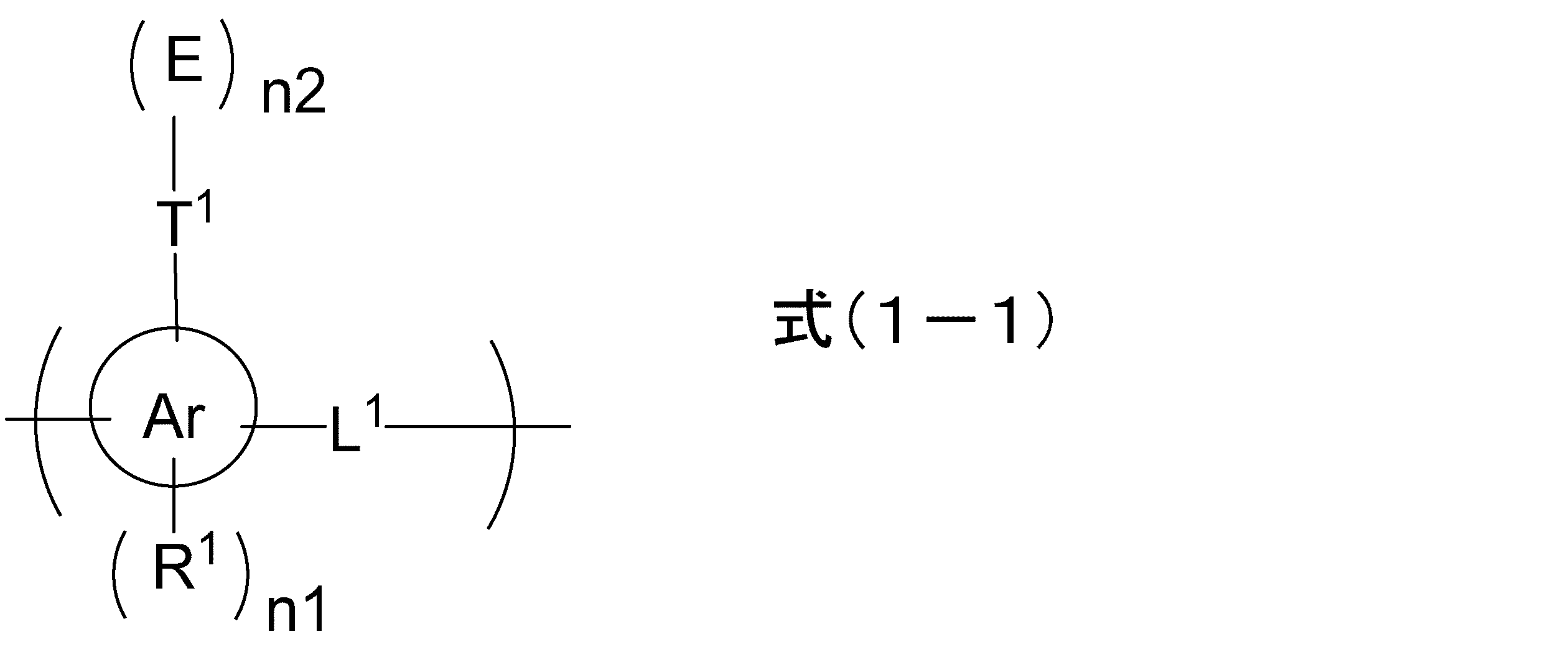
(式(1-1)中、Arはベンゼン環、ナフタレン環又はアントラセン環を表し、R1はヒドロキシ基、メチル基で保護されていてもよいメルカプト基、メチル基で保護されていてもよいアミノ基、ハロゲノ基又は、ヘテロ原子で置換若しくは中断されていてもよくヒドロキシ基で置換されていてもよい炭素原子数1~10のアルキル基を表し、n1は0~3の整数を表し、L1は単結合又は炭素原子数1~10のアルキレン基を表し、Eはエポキシ基を表し、T1はn2=1のとき、単結合又は、エーテル結合、エステル結合若しくはアミド結合で中断されていてもよい炭素原子数1~10のアルキレン基を表し、T1はn2=2のとき、窒素原子又はアミド結合を表す)、
(B)カテコール以外のフェノール性ヒドロキシ基を有する化合物又は重合体、
(C)熱酸発生剤、及び
(D)溶剤、
を含む、半導体用ウエットエッチング液に対する保護膜形成組成物。
(式(1-1)中、Arはベンゼン環、ナフタレン環又はアントラセン環を表し、R1はヒドロキシ基、メチル基で保護されていてもよいメルカプト基、メチル基で保護されていてもよいアミノ基、ハロゲノ基又は、ヘテロ原子で置換若しくは中断されていてもよくヒドロキシ基で置換されていてもよい炭素原子数1~10のアルキル基を表し、n1は0~3の整数を表し、L1は単結合又は炭素原子数1~10のアルキレン基を表し、Eはエポキシ基を表し、T1はn2=1のとき、単結合又は、エーテル結合、エステル結合若しくはアミド結合で中断されていてもよい炭素原子数1~10のアルキレン基を表し、T1はn2=2のとき、窒素原子又はアミド結合を表す)、
(B)カテコール以外のフェノール性ヒドロキシ基を有する化合物又は重合体、
(C)熱酸発生剤、及び
(D)溶剤、
を含む、半導体用ウエットエッチング液に対する保護膜形成組成物。
[2] 前記(B)化合物又は重合体が、2以上のフェノール性ヒドロキシ基を有する、[1]に記載の保護膜形成組成物。
[3] 前記(B)化合物又は重合体が、下記式(2-1)で表される、[1]又は[2]に記載の保護膜形成組成物:
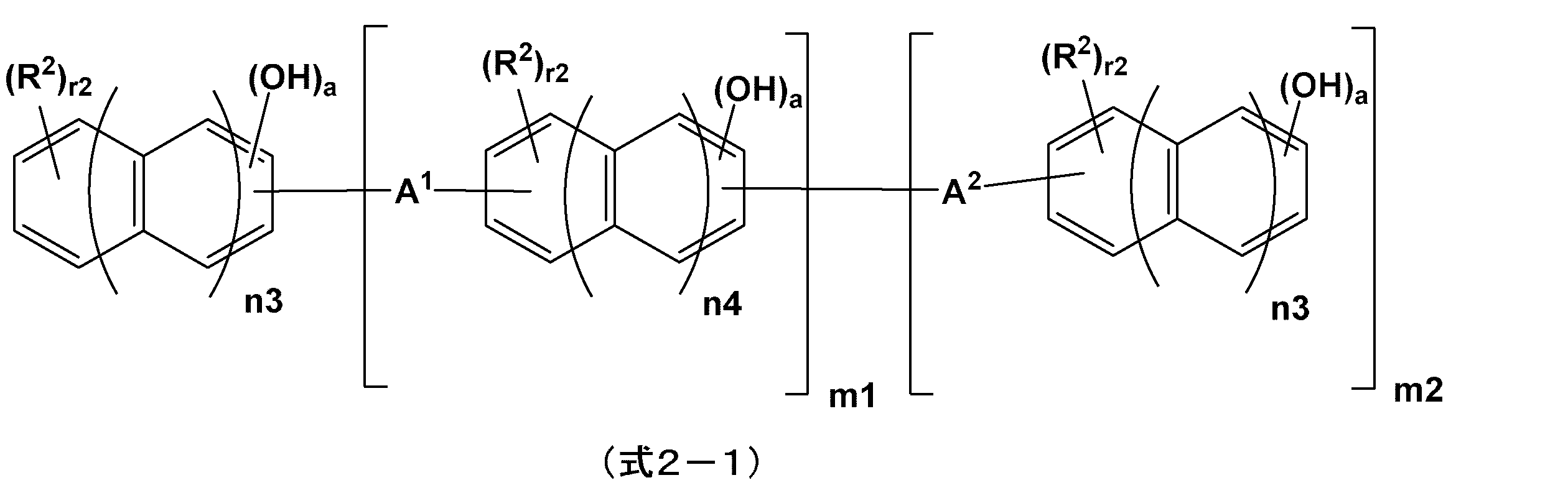
(式中、R2及びT2は各々独立して、ハロゲノ基、カルボキシ基、ニトロ基、シアノ基、メチレンジオキシ基、アセトキシ基、メチルチオ基、炭素原子数1~9のアルコキシ基、炭素原子数1~3のアルキル基で置換されていてもよいアミノ基、ヒドロキシ基又はハロゲノ基で置換されていてもよい炭素原子数1~10のアルキル基を表す。A1とA2は各々独立して、炭素原子数1~10のアルキレン基、ビシクロ環化合物由来の2価の有機基、ビフェニレン基又は-CT2T3-で表される2価の有機基又はそれらの組み合わせであり、T3は水素原子又は(式2-1-a)で表される1価の基を表す:
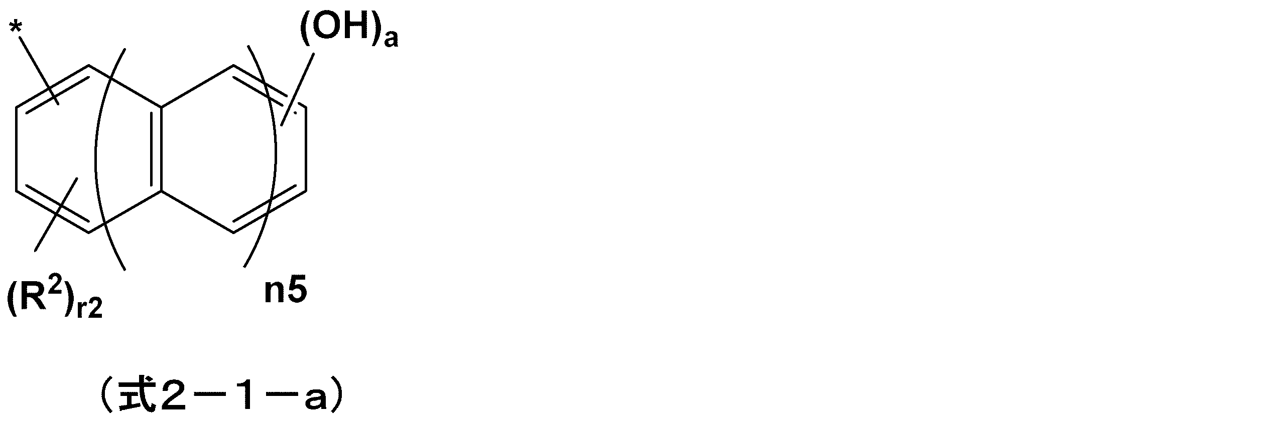
(式2-1-a)中の*は、T3が結合する炭素原子との結合部位を表す。aは1~6の整数を表す。
n3~n5は各々独立して0~2の整数を表す。r2は0~3の整数を表す。m1とm2は各々独立して0~10,000,000の数を表す。)
(式中、R2及びT2は各々独立して、ハロゲノ基、カルボキシ基、ニトロ基、シアノ基、メチレンジオキシ基、アセトキシ基、メチルチオ基、炭素原子数1~9のアルコキシ基、炭素原子数1~3のアルキル基で置換されていてもよいアミノ基、ヒドロキシ基又はハロゲノ基で置換されていてもよい炭素原子数1~10のアルキル基を表す。A1とA2は各々独立して、炭素原子数1~10のアルキレン基、ビシクロ環化合物由来の2価の有機基、ビフェニレン基又は-CT2T3-で表される2価の有機基又はそれらの組み合わせであり、T3は水素原子又は(式2-1-a)で表される1価の基を表す:
(式2-1-a)中の*は、T3が結合する炭素原子との結合部位を表す。aは1~6の整数を表す。
n3~n5は各々独立して0~2の整数を表す。r2は0~3の整数を表す。m1とm2は各々独立して0~10,000,000の数を表す。)
[4] 前記m1、n3~n5及びr2が0であり、m2が1である、[3]に記載の保護膜形成組成物。
[5] 前記(B)化合物又は重合体が、下記式(2-2)で表される化合物である、[1]又は[2]に記載の保護膜形成組成物:

(式中、R3はハロゲノ基、カルボキシ基、ニトロ基、シアノ基、メチレンジオキシ基、アセトキシ基、メチルチオ基、炭素原子数1~9のアルコキシ基、炭素原子数1~3のアルキル基で置換されていてもよいアミノ基、ヒドロキシ基又はハロゲノ基で置換されていてもよい炭素原子数1~10のアルキル基を表す。Q1は単結合、酸素原子、硫黄原子、スルホニル基、カルボニル基、イミノ基、炭素原子数6~40のアリーレン基、ハロゲノ基で置換されていてもよい炭素原子数1~10のアルキレン基を表す。aは1~6の整数を表す。n6は0~2の整数を表す。r3は0~3の整数を表す。)
(式中、R3はハロゲノ基、カルボキシ基、ニトロ基、シアノ基、メチレンジオキシ基、アセトキシ基、メチルチオ基、炭素原子数1~9のアルコキシ基、炭素原子数1~3のアルキル基で置換されていてもよいアミノ基、ヒドロキシ基又はハロゲノ基で置換されていてもよい炭素原子数1~10のアルキル基を表す。Q1は単結合、酸素原子、硫黄原子、スルホニル基、カルボニル基、イミノ基、炭素原子数6~40のアリーレン基、ハロゲノ基で置換されていてもよい炭素原子数1~10のアルキレン基を表す。aは1~6の整数を表す。n6は0~2の整数を表す。r3は0~3の整数を表す。)
[6] 前記(B)化合物又は重合体が、下記式(3-1)で表される単位構造を含む重合体である、[1]又は[2]に記載の保護膜形成組成物:

(式中、T4はハロゲノ基で置換されていてもよい炭素原子数1~10のアルキル基を表す。R4はハロゲノ基、カルボキシ基、ニトロ基、シアノ基、メチレンジオキシ基、アセトキシ基、メチルチオ基、炭素原子数1~9のアルコキシ基、炭素原子数1~3のアルキル基で置換されていてもよいアミノ基、ヒドロキシ基又はハロゲノ基で置換されていてもよい炭素原子数1~10のアルキル基を表す。r4は0~3の整数を表す。n7は0~2の整数を表す。aは1~6の整数を表す。)
(式中、T4はハロゲノ基で置換されていてもよい炭素原子数1~10のアルキル基を表す。R4はハロゲノ基、カルボキシ基、ニトロ基、シアノ基、メチレンジオキシ基、アセトキシ基、メチルチオ基、炭素原子数1~9のアルコキシ基、炭素原子数1~3のアルキル基で置換されていてもよいアミノ基、ヒドロキシ基又はハロゲノ基で置換されていてもよい炭素原子数1~10のアルキル基を表す。r4は0~3の整数を表す。n7は0~2の整数を表す。aは1~6の整数を表す。)
[7] [1]~[6]のいずれか1項に記載の保護膜形成組成物からなる塗布膜の焼成物であることを特徴とする半導体用ウエットエッチング液に対する保護膜。
[8] (A)下記式(1-1)で表される単位構造を有する重合体:

(式(1-1)中、Arはベンゼン環、ナフタレン環又はアントラセン環を表し、R1はヒドロキシ基、メチル基で保護されていてもよいメルカプト基、メチル基で保護されていてもよいアミノ基、ハロゲノ基又は、ヘテロ原子で置換若しくは中断されていてもよくヒドロキシ基で置換されていてもよい炭素原子数1~10のアルキル基を表し、n1は0~3の整数を表し、L1は単結合又は炭素原子数1~10のアルキレン基を表し、Eはエポキシ基を表し、T1はn2=1のとき、単結合又は、エーテル結合、エステル結合若しくはアミド結合で中断されていてもよい炭素原子数1~10のアルキレン基を表し、T1はn2=2のとき、窒素原子又はアミド結合を表す)、
(B)カテコール以外のフェノール性ヒドロキシ基を有する化合物又は重合体、
(C)熱酸発生剤、及び
(D)溶剤、
を含む、レジスト下層膜形成組成物。
(式(1-1)中、Arはベンゼン環、ナフタレン環又はアントラセン環を表し、R1はヒドロキシ基、メチル基で保護されていてもよいメルカプト基、メチル基で保護されていてもよいアミノ基、ハロゲノ基又は、ヘテロ原子で置換若しくは中断されていてもよくヒドロキシ基で置換されていてもよい炭素原子数1~10のアルキル基を表し、n1は0~3の整数を表し、L1は単結合又は炭素原子数1~10のアルキレン基を表し、Eはエポキシ基を表し、T1はn2=1のとき、単結合又は、エーテル結合、エステル結合若しくはアミド結合で中断されていてもよい炭素原子数1~10のアルキレン基を表し、T1はn2=2のとき、窒素原子又はアミド結合を表す)、
(B)カテコール以外のフェノール性ヒドロキシ基を有する化合物又は重合体、
(C)熱酸発生剤、及び
(D)溶剤、
を含む、レジスト下層膜形成組成物。
[9] [8]に記載のレジスト下層膜形成組成物からなる塗布膜の焼成物であることを特徴とするレジスト下層膜。
[10] [1]~[6]のいずれか1項に記載の保護膜形成組成物を、段差を有する半導体基板上に塗布し焼成して保護膜を形成する工程を含む、半導体の製造に用いることを特徴とする保護膜付き基板の製造方法。
[11] [1]~[6]のいずれか1項に記載の保護膜組成物又は[8]に記載のレジスト下層膜形成組成物を半導体基板上に塗布し焼成してレジスト下層膜としての保護膜を形成する工程、該保護膜上にレジスト膜を形成し、次いで露光、現像してレジストパターンを形成する工程を含み、半導体の製造に用いることを特徴とするレジストパターン付き基板の製造方法。
[12] 表面に無機膜が形成されていてもよい半導体基板上に、[1]~[6]のいずれか1項に記載の保護膜形成組成物を用いて保護膜を形成し、前記保護膜上にレジストパターンを形成し、前記レジストパターンをマスクとして前記保護膜をドライエッチングし、前記無機膜又は前記半導体基板の表面を露出させ、ドライエッチング後の前記保護膜をマスクとして、半導体用ウエットエッチング液を用いて前記無機膜又は前記半導体基板をウエットエッチング及び洗浄する工程を含む半導体装置の製造方法。
[13] 表面に無機膜が形成されていてもよい半導体基板上に、[8]に記載のレジスト下層膜形成組成物を用いてレジスト下層膜を形成し、前記レジスト下層膜上にレジストパターンを形成し、前記レジストパターンをマスクとして前記レジスト下層膜をドライエッチングし、前記無機膜又は前記半導体基板の表面を露出させ、ドライエッチング後の前記レジスト下層膜をマスクとして、前記無機膜又は前記半導体基板をエッチングする工程を含む半導体装置の製造方法。
本発明の保護膜形成組成物は、半導体製造におけるリソグラフィープロセスにおいて、例えば下記の特性をバランス良く有していることが要求される。(1)下地基板加工時にウエットエッチング液に対する良好なマスク機能を有すること、(2)さらに低ドライエッチング速度により基板加工時の保護膜又はレジスト下層膜へのダメージを低減すること、(3)段差基板の平坦化性に優れること、(4)微細なトレンチパターン基板への埋め込み性に優れること、これら(1)~(4)の性能をバランスよく有することで、半導体基板の微細加工を容易に行うことができる。
<半導体用ウエットエッチング液に対する保護膜形成組成物>
本発明の半導体用ウエットエッチング液に対する保護膜形成組成物は、
(A)下記式(1-1)で表される単位構造を有する重合体:
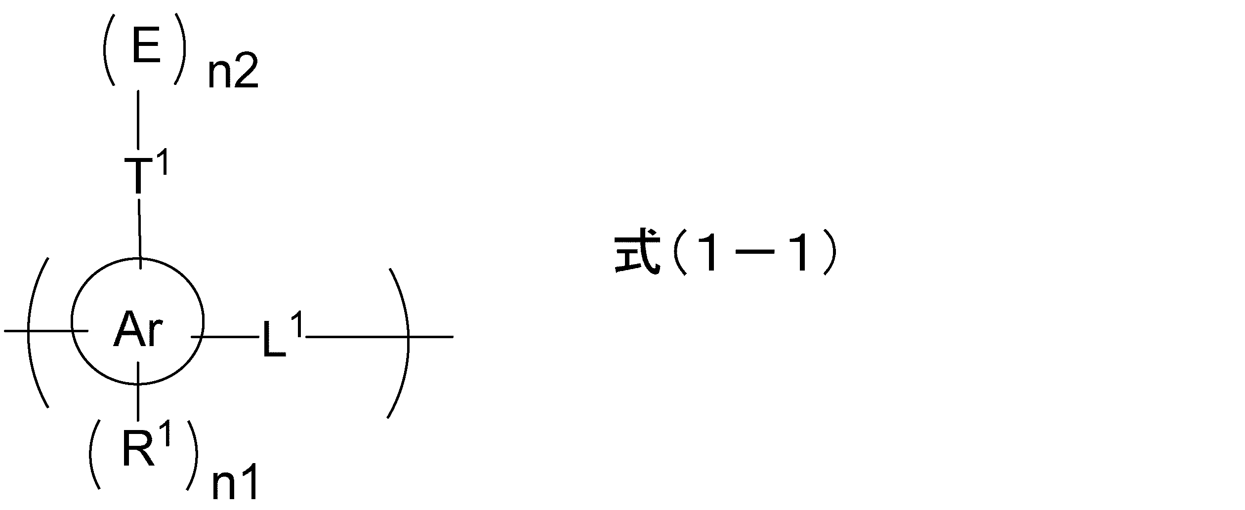
(式(1-1)中、Arはベンゼン環、ナフタレン環又はアントラセン環を表し、R1はヒドロキシ基、メチル基で保護されていてもよいメルカプト基、メチル基で保護されていてもよいアミノ基、ハロゲノ基又は、ヘテロ原子で置換若しくは中断されていてもよくヒドロキシ基で置換されていてもよい炭素原子数1~10のアルキル基を表し、n1は0~3の整数を表し、L1は単結合又は炭素原子数1~10のアルキレン基を表し、Eはエポキシ基を表し、T1はn2=1のとき、単結合又は、エーテル結合、エステル結合若しくはアミド結合で中断されていてもよい炭素原子数1~10のアルキレン基を表し、T1はn2=2のとき、窒素原子又はアミド結合を表す)、
(B)カテコール以外のフェノール性ヒドロキシ基を有する化合物又は重合体、
(C)熱酸発生剤、及び
(D)溶剤、
を含む。
本発明の半導体用ウエットエッチング液に対する保護膜形成組成物は、
(A)下記式(1-1)で表される単位構造を有する重合体:
(式(1-1)中、Arはベンゼン環、ナフタレン環又はアントラセン環を表し、R1はヒドロキシ基、メチル基で保護されていてもよいメルカプト基、メチル基で保護されていてもよいアミノ基、ハロゲノ基又は、ヘテロ原子で置換若しくは中断されていてもよくヒドロキシ基で置換されていてもよい炭素原子数1~10のアルキル基を表し、n1は0~3の整数を表し、L1は単結合又は炭素原子数1~10のアルキレン基を表し、Eはエポキシ基を表し、T1はn2=1のとき、単結合又は、エーテル結合、エステル結合若しくはアミド結合で中断されていてもよい炭素原子数1~10のアルキレン基を表し、T1はn2=2のとき、窒素原子又はアミド結合を表す)、
(B)カテコール以外のフェノール性ヒドロキシ基を有する化合物又は重合体、
(C)熱酸発生剤、及び
(D)溶剤、
を含む。
<重合体(A)>
本発明で使用される重合体(A)は、下記式(1-1)で表される単位構造を有する重合体である:
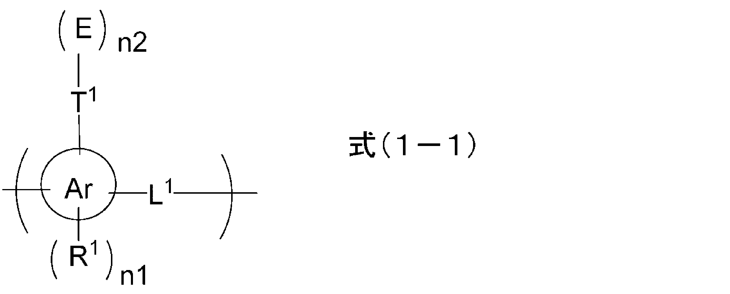
(式(1-1)中、Arはベンゼン環、ナフタレン環又はアントラセン環を表し、R1は前記ベンゼン環、ナフタレン環又はアントラセン環が含む水素原子の置換基としてのヒドロキシ基、メチル基で保護されていてもよいメルカプト基、メチル基で保護されていてもよいアミノ基、ハロゲノ基又は、ヘテロ原子で置換若しくは中断されていてもよくヒドロキシ基で置換されていてもよい炭素原子数1~10のアルキル基を表し、n1は0~3の整数を表し、L1は単結合又は炭素原子数1~10のアルキレン基を表し、Eはエポキシ基を表し、T1はn2=1のとき、単結合又は、エーテル結合、エステル結合若しくはアミド結合で中断されていてもよい炭素原子数1~10のアルキレン基を表し、T1はn2=2のとき、窒素原子又はアミド結合を表す。)
本発明で使用される重合体(A)は、下記式(1-1)で表される単位構造を有する重合体である:
(式(1-1)中、Arはベンゼン環、ナフタレン環又はアントラセン環を表し、R1は前記ベンゼン環、ナフタレン環又はアントラセン環が含む水素原子の置換基としてのヒドロキシ基、メチル基で保護されていてもよいメルカプト基、メチル基で保護されていてもよいアミノ基、ハロゲノ基又は、ヘテロ原子で置換若しくは中断されていてもよくヒドロキシ基で置換されていてもよい炭素原子数1~10のアルキル基を表し、n1は0~3の整数を表し、L1は単結合又は炭素原子数1~10のアルキレン基を表し、Eはエポキシ基を表し、T1はn2=1のとき、単結合又は、エーテル結合、エステル結合若しくはアミド結合で中断されていてもよい炭素原子数1~10のアルキレン基を表し、T1はn2=2のとき、窒素原子又はアミド結合を表す。)
前記炭素原子数1~10のアルキル基としては、メチル基、エチル基、n-プロピル基、i-プロピル基、シクロプロピル基、n-ブチル基、i-ブチル基、s-ブチル基、t-ブチル基、シクロブチル基、1-メチル-シクロプロピル基、2-メチル-シクロプロピル基、n-ペンチル基、1-メチル-n-ブチル基、2-メチル-n-ブチル基、3-メチル-n-ブチル基、1,1-ジメチル-n-プロピル基、1,2-ジメチル-n-プロピル基、2,2-ジメチル-n-プロピル基、1-エチル-n-プロピル基、シクロペンチル基、1-メチル-シクロブチル基、2-メチル-シクロブチル基、3-メチル-シクロブチル基、1,2-ジメチル-シクロプロピル基、2,3-ジメチル-シクロプロピル基、1-エチル-シクロプロピル基、2-エチル-シクロプロピル基、n-ヘキシル基、1-メチル-n-ペンチル基、2-メチル-n-ペンチル基、3-メチル-n-ペンチル基、4-メチル-n-ペンチル基、1,1-ジメチル-n-ブチル基、1,2-ジメチル-n-ブチル基、1,3-ジメチル-n-ブチル基、2,2-ジメチル-n-ブチル基、2,3-ジメチル-n-ブチル基、3,3-ジメチル-n-ブチル基、1-エチル-n-ブチル基、2-エチル-n-ブチル基、1,1,2-トリメチル-n-プロピル基、1,2,2-トリメチル-n-プロピル基、1-エチル-1-メチル-n-プロピル基、1-エチル-2-メチル-n-プロピル基、シクロヘキシル基、1-メチル-シクロペンチル基、2-メチル-シクロペンチル基、3-メチル-シクロペンチル基、1-エチル-シクロブチル基、2-エチル-シクロブチル基、3-エチル-シクロブチル基、1,2-ジメチル-シクロブチル基、1,3-ジメチル-シクロブチル基、2,2-ジメチル-シクロブチル基、2,3-ジメチル-シクロブチル基、2,4-ジメチル-シクロブチル基、3,3-ジメチル-シクロブチル基、1-n-プロピル-シクロプロピル基、2-n-プロピル-シクロプロピル基、1-i-プロピル-シクロプロピル基、2-i-プロピル-シクロプロピル基、1,2,2-トリメチル-シクロプロピル基、1,2,3-トリメチル-シクロプロピル基、2,2,3-トリメチル-シクロプロピル基、1-エチル-2-メチル-シクロプロピル基、2-エチル-1-メチル-シクロプロピル基、2-エチル-2-メチル-シクロプロピル基、2-エチル-3-メチル-シクロプロピル基、デシル基、メトキシ基、エトキシ基、メトキシメチル基、エトキシメチル基、メトキシエチル基、エトキシエチル基、ヒドロキシメチル基、1-ヒドロキシエチル基、2-ヒドロキシエチル基、メチルアミノ基、ジメチルアミノ基、ジエチルアミノ基、アミノメチル基、1-アミノエチル基、2-アミノエチル基、メチルチオ基、エチルチオ基、メルカプトメチル基、1-メルカプトエチル基、2-メルカプトエチル基、等が挙げられる。
前記炭素原子数1~10のアルキレン基としては、メチレン基、エチレン基、n-プロピレン基、イソプロピレン基、シクロプロピレン基、n-ブチレン基、イソブチレン基、s-ブチレン基、t-ブチレン基、シクロブチレン基、1-メチル-シクロプロピレン基、2-メチル-シクロプロピレン基、n-ペンチレン基、1-メチル-n-ブチレン基、2-メチル-n-ブチレン基、3-メチル-n-ブチレン基、1,1-ジメチル-n-プロピレン基、1,2-ジメチル-n-プロピレン基、2,2-ジメチル-n-プロピレン、1-エチル-n-プロピレン基、シクロペンチレン基、1-メチル-シクロブチレン基、2-メチル-シクロブチレン基、3-メチル-シクロブチレン基、1,2-ジメチル-シクロプロピレン基、2,3-ジメチル-シクロプロピレン基、1-エチル-シクロプロピレン基、2-エチル-シクロプロピレン基、n-ヘキシレン基、1-メチル-n-ペンチレン基、2-メチル-n-ペンチレン基、3-メチル-n-ペンチレン基、4-メチル-n-ペンチレン基、1,1-ジメチル-n-ブチレン基、1,2-ジメチル-n-ブチレン基、1,3-ジメチル-n-ブチレン基、2,2-ジメチル-n-ブチレン基、2,3-ジメチル-n-ブチレン基、3,3-ジメチル-n-ブチレン基、1-エチル-n-ブチレン基、2-エチル-n-ブチレン基、1,1,2-トリメチル-n-プロピレン基、1,2,2-トリメチル-n-プロピレン基、1-エチル-1-メチル-n-プロピレン基、1-エチル-2-メチル-n-プロピレン基、シクロヘキシレン基、1-メチル-シクロペンチレン基、2-メチル-シクロペンチレン基、3-メチル-シクロペンチレン基、1-エチル-シクロブチレン基、2-エチル-シクロブチレン基、3-エチル-シクロブチレン基、1,2-ジメチル-シクロブチレン基、1,3-ジメチル-シクロブチレン基、2,2-ジメチル-シクロブチレン基、2,3-ジメチル-シクロブチレン基、2,4-ジメチル-シクロブチレン基、3,3-ジメチル-シクロブチレン基、1-n-プロピル-シクロプロピレン基、2-n-プロピル-シクロプロピレン基、1-イソプロピル-シクロプロピレン基、2-イソプロピル-シクロプロピレン基、1,2,2-トリメチル-シクロプロピレン基、1,2,3-トリメチル-シクロプロピレン基、2,2,3-トリメチル-シクロプロピレン基、1-エチル-2-メチル-シクロプロピレン基、2-エチル-1-メチル-シクロプロピレン基、2-エチル-2-メチル-シクロプロピレン基、2-エチル-3-メチル-シクロプロピレン基、n-ヘプチレン基、n-オクチレン基、n-ノニレン基又はn-デカニレン基が挙げられる。
前記R1は、炭素原子数1~10のアルコキシ基であってもよい。
炭素原子数1~10のアルコキシ基としては、メトキシ基、エトキシ基、n-プロポキシ基、i-プロポキシ基、n-ブトキシ基、i-ブトキシ基、s-ブトキシ基、t-ブトキシ基、n-ペントキシ基、1-メチル-n-ブトキシ基、2-メチル-n-ブトキシ基、3-メチル-n-ブトキシ基、1,1-ジメチル-n-プロポキシ基、1,2-ジメチル-n-プロポキシ基、2,2-ジメチル-n-プロポキシ基、1-エチル-n-プロポキシ基、n-ヘキシルオキシ基、1-メチル-n-ペンチルオキシ基、2-メチル-n-ペンチルオキシ基、3-メチル-n-ペンチルオキシ基、4-メチル-n-ペンチルオキシ基、1,1-ジメチル-n-ブトキシ基、1,2-ジメチル-n-ブトキシ基、1,3-ジメチル-n-ブトキシ基、2,2-ジメチル-n-ブトキシ基、2,3-ジメチル-n-ブトキシ基、3,3-ジメチル-n-ブトキシ基、1-エチル-n-ブトキシ基、2-エチル-n-ブトキシ基、1,1,2-トリメチル-n-プロポキシ基、1,2,2,-トリメチル-n-プロポキシ基、1-エチル-1-メチル-n-プロポキシ基、1-エチル-2-メチル-n-プロポキシ基、n-ヘプチルオキシ基、n-オクチルオキシ基及びn-ノニルオキシ基等が挙げられる。
前記式(1-1)で表される単位構造は、1種類でも2種以上の組み合わせでもよい。例えばArが同一種類である複数の単位構造を有する共重合体であってもよく、例えばArがベンゼン環を含む単位構造と、ナフタレン環とを有する単位構造を有するような、Arの種類が異なる、複数の単位構造を有する共重合体も本願の技術範囲から排除されない。
前記「中断されていてもよい」、とは炭素原子数2~10のアルキレン基の場合、前記アルキレン基中の何れかの炭素―炭素原子間がヘテロ原子(すなわち酸素の場合はエーテル結合、硫黄の場合はスルフィド結合)、エステル結合若しくはアミド結合で中断されていることを言い、炭素原子数1(すなわちメチレン基)では、メチレン基の炭素のどちらか一方にヘテロ原子(すなわち酸素の場合はエーテル結合、硫黄の場合はスルフィド結合)、エステル結合若しくはアミド結合を有することを言う。
前記T1はn2=1のとき、単結合又は、エーテル結合、エステル結合若しくはアミド結合で中断されていてもよい炭素原子数1~10のアルキレン基を表すが、エーテル結合とメチレン基との組み合わせ(すなわち式(1-1)の「-T1-(E)n2」がグリシジルエーテル基の場合)、エステル結合とメチレン基との組み合わせ、又はアミド結合とメチレン基との組み合わせであることが好ましい。
ヘテロ原子で置換されていてもよい炭素原子数1~10のアルキル基とは、前記炭素原子数1~10のアルキル基が有する1つ以上の水素原子が、ヘテロ原子(好ましくはハロゲノ基)で置換されていることをいう。
前記L1は単結合又は炭素原子数1~10のアルキレン基を表すが、下記式(1-2):

(式(1-2)中、R2、R3は、互いに独立して水素原子、メチル基、エチル基、n-プロピル基、i-プロピル基、シクロプロピル基、n-ブチル基、i-ブチル基、s-ブチル基、t-ブチル基、シクロブチル基を表し、R2、R3は互いに結合して炭素原子数3~6の環を形成してもよい)で表されることが好ましい。これらの中でもR2、R3いずれも水素原子(すなわち―(CR2R3)―がメチレン基)であることが好ましい。
(式(1-2)中、R2、R3は、互いに独立して水素原子、メチル基、エチル基、n-プロピル基、i-プロピル基、シクロプロピル基、n-ブチル基、i-ブチル基、s-ブチル基、t-ブチル基、シクロブチル基を表し、R2、R3は互いに結合して炭素原子数3~6の環を形成してもよい)で表されることが好ましい。これらの中でもR2、R3いずれも水素原子(すなわち―(CR2R3)―がメチレン基)であることが好ましい。
前記ハロゲノ基とは、水素と置換したハロゲン-X(F、Cl、Br、I)をいう。
前記重合体(A)は、前記式(1-1)の単位構造を満たすものであれば、特に制限されない。自体公知の方法で製造されたものでよい。市販品を使用してもよい。市販品としては、耐熱性エポキシノボラック樹脂EOCN(登録商標)シリーズ(日本化薬(株)製、エポキシノボラック樹脂D.E.N(登録商標)シリーズ(ダウ・ケミカル日本(株)製)等が挙げられる。
前記重合体(A)の重量平均分子量としては100以上であり、500~200,000であり、600~50,000であり、又は700~10,000である。
本願の重合体(A)としては、下記の単位構造を有するものが挙げられる。

<(B)カテコール以外のフェノール性ヒドロキシ基を有する化合物又は重合体>
前記カテコール以外のフェノール性ヒドロキシ基を有する化合物又は重合体(B)は、本願発明の効果を損ねない化合物又は重合体であれば特に限定されない。言うまでもなく、前記カテコール以外のフェノール性ヒドロキシ基を有する化合物又は重合体(B)は前記重合体(A)とは異なる。
前記カテコール以外のフェノール性ヒドロキシ基を有する化合物又は重合体(B)は、本願発明の効果を損ねない化合物又は重合体であれば特に限定されない。言うまでもなく、前記カテコール以外のフェノール性ヒドロキシ基を有する化合物又は重合体(B)は前記重合体(A)とは異なる。
前記カテコール以外のフェノール性ヒドロキシ基を有する化合物又は重合体(B)の重量平均分子量も特に制限されないが、例えば300~50,000である。
前記(B)化合物又は重合体が、2以上のフェノール性ヒドロキシ基を有することが好ましい。
[1]式(2-1)で表される化合物又は重合体
前記(B)化合物が、下記式(2-1)で表されることが好ましい:

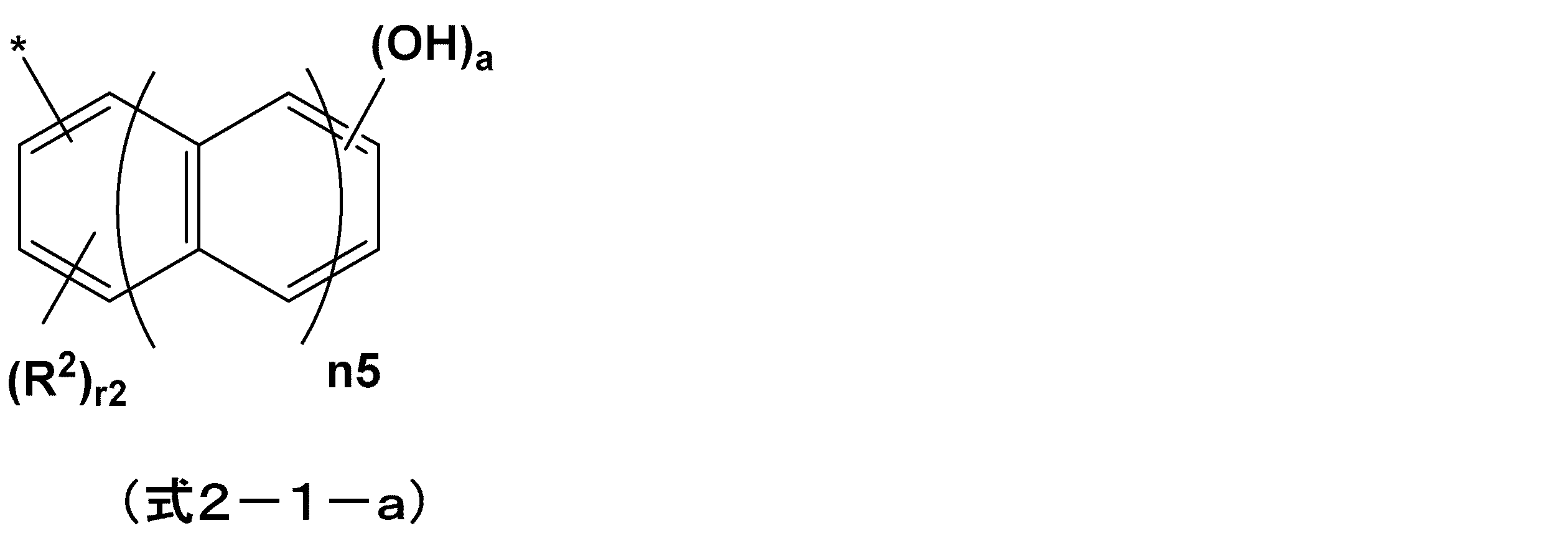
(式中、R2及びT2は各々独立して、ハロゲノ基、カルボキシ基、ニトロ基、シアノ基、メチレンジオキシ基、アセトキシ基、メチルチオ基、炭素原子数1~9のアルコキシ基、炭素原子数1~3のアルキル基で置換されてもよいアミノ基、ヒドロキシ基又はハロゲノ基で置換されていてもよい炭素原子数1~10のアルキル基を表す。A1とA2は各々独立して、炭素原子数1~10のアルキレン基、ビシクロ環化合物由来の2価の有機基、ビフェニレン基又は-CT2T3-で表される2価の有機基又はそれらの組み合わせであり、T3は水素原子又は(式2-1-a)で表される1価の基を表す。(式2-1-a)中の*は、T3が結合する炭素原子との結合部位を表す。aは1~6の整数を表す。n3~n5は各々独立して0~2の整数を表す。r2は0~3の整数を表す。m1とm2は各々独立して0~10,000,000を表す。)
前記m1、n3~n5及びr2が0であり、m2が1であることが好ましい。
前記(B)化合物が、下記式(2-1)で表されることが好ましい:
(式中、R2及びT2は各々独立して、ハロゲノ基、カルボキシ基、ニトロ基、シアノ基、メチレンジオキシ基、アセトキシ基、メチルチオ基、炭素原子数1~9のアルコキシ基、炭素原子数1~3のアルキル基で置換されてもよいアミノ基、ヒドロキシ基又はハロゲノ基で置換されていてもよい炭素原子数1~10のアルキル基を表す。A1とA2は各々独立して、炭素原子数1~10のアルキレン基、ビシクロ環化合物由来の2価の有機基、ビフェニレン基又は-CT2T3-で表される2価の有機基又はそれらの組み合わせであり、T3は水素原子又は(式2-1-a)で表される1価の基を表す。(式2-1-a)中の*は、T3が結合する炭素原子との結合部位を表す。aは1~6の整数を表す。n3~n5は各々独立して0~2の整数を表す。r2は0~3の整数を表す。m1とm2は各々独立して0~10,000,000を表す。)
前記m1、n3~n5及びr2が0であり、m2が1であることが好ましい。
前記式(2-1)に係るハロゲノ基、アルコキシ基及びアルキル基の説明は、前述の通りである。
前記ビシクロ環化合物としては、ジシクロペンタジエン、置換ジシクロペンタジエン、テトラシクロ[4.4.0.12,5.17,10]ドデカ-3,8-ジエン、又は置換テトラシクロ[4.4.0.12,5.17,10]ドデカ-3,8-ジエンが挙げられる。前記置換とは、前記ビシクロ環化合物の1つ又は2つ以上の水素原子が、それぞれ独立にハロゲノ基、ニトロ基、アミノ基若しくはヒドロキシ基又はそれらの基で置換されていても良い炭素原子数1~10のアルキル基若しくは炭素原子数6~40のアリール基で置換されていることをいう。ビシクロ環化合物由来の2価の有機基とは、前記ビシクロ環化合物から任意の2つの水素原子を取り去ることによって誘導される、結合手を2つ有する基をいう。
前記炭素原子数6~40のアリール基としては、フェニル基、o-メチルフェニル基、m-メチルフェニル基、p-メチルフェニル基、o-クロルフェニル基、m-クロルフェニル基、p-クロルフェニル基、o-フルオロフェニル基、p-フルオロフェニル基、o-メトキシフェニル基、p-メトキシフェニル基、p-ニトロフェニル基、p-シアノフェニル基、α-ナフチル基、β-ナフチル基、o-ビフェニリル基、m-ビフェニリル基、p-ビフェニリル基、1-アントリル基、2-アントリル基、9-アントリル基、1-フェナントリル基、2-フェナントリル基、3-フェナントリル基、4-フェナントリル基及び9-フェナントリル基が挙げられる。
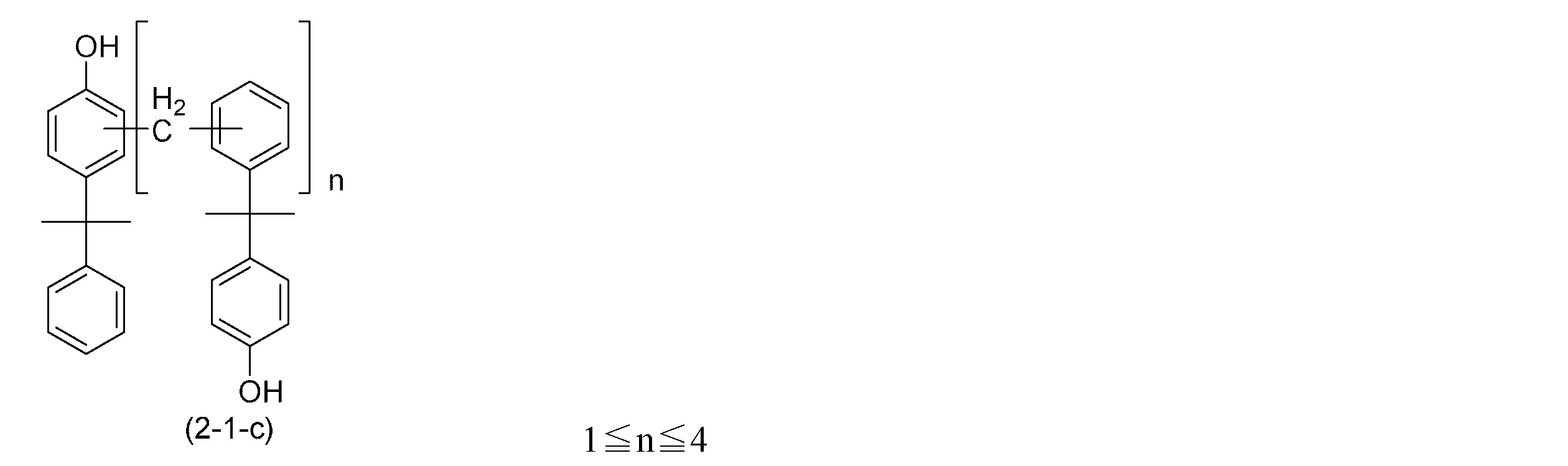
前記式(2-1)で表される化合物の具体例としては、以下に記載の化合物が挙げられる。

上記(B)カテコール以外のフェノール性ヒドロキシ基を有する化合物は、以下に示される化合物であってよい。
[2] 式(2-2)で表される化合物
前記(B)化合物は、(B)カテコール以外のフェノール性ヒドロキシ基を有する化合物であり、本願発明の効果を損ねない化合物であれば特に限定されないが、前記(B)化合物が、下記式(2-2)で表されることが好ましい:

(式中、R3はハロゲノ基、カルボキシ基、ニトロ基、シアノ基、メチレンジオキシ基、アセトキシ基、メチルチオ基、炭素原子数1~9のアルコキシ基、炭素原子数1~3のアルキル基で置換されていてもよいアミノ基、ヒドロキシ基又はハロゲノ基で置換されていてもよい炭素原子数1~10のアルキル基を表す。Q1は単結合、酸素原子、硫黄原子、スルホニル基、カルボニル基、イミノ基、炭素原子数6~40のアリーレン基、ハロゲノ基で置換されていてもよい炭素原子数1~10のアルキレン基を表す。aは1~6の整数を表す。n6は0~2の整数を表す。r3は0~3の整数を表す。)
式(2-2)のアルコキシ基、アルキル基及びハロゲノ基の説明は前述の通りである。
前記(B)化合物は、(B)カテコール以外のフェノール性ヒドロキシ基を有する化合物であり、本願発明の効果を損ねない化合物であれば特に限定されないが、前記(B)化合物が、下記式(2-2)で表されることが好ましい:
(式中、R3はハロゲノ基、カルボキシ基、ニトロ基、シアノ基、メチレンジオキシ基、アセトキシ基、メチルチオ基、炭素原子数1~9のアルコキシ基、炭素原子数1~3のアルキル基で置換されていてもよいアミノ基、ヒドロキシ基又はハロゲノ基で置換されていてもよい炭素原子数1~10のアルキル基を表す。Q1は単結合、酸素原子、硫黄原子、スルホニル基、カルボニル基、イミノ基、炭素原子数6~40のアリーレン基、ハロゲノ基で置換されていてもよい炭素原子数1~10のアルキレン基を表す。aは1~6の整数を表す。n6は0~2の整数を表す。r3は0~3の整数を表す。)
式(2-2)のアルコキシ基、アルキル基及びハロゲノ基の説明は前述の通りである。
炭素原子数6~40のアリーレン基としては、フェニレン基、o-メチルフェニレン基、m-メチルフェニレン基、p-メチルフェニレン基、o-クロルフェニレン基、m-クロルフェニレン基、p-クロルフェニレン基、o-フルオロフェニレン基、p-フルオロフェニレン基、o-メトキシフェニレン基、p-メトキシフェニレン基、p-ニトロフェニレン基、p-シアノフェニレン基、α-ナフチレン基、β-ナフチレン基、o-ビフェニリレン基、m-ビフェニリレン基、p-ビフェニリレン基、1-アントリレン基、2-アントリレン基、9-アントリレン基、1-フェナントリレン基、2-フェナントリレン基、3-フェナントリレン基、4-フェナントリレン基及び9-フェナントリレン基が挙げられる。
炭素原子数1~10のアルキレン基としては、メチレン基、エチレン基、n-プロピレン基、イソプロピレン基、シクロプロピレン基、n-ブチレン基、イソブチレン基、s-ブチレン基、t-ブチレン基、シクロブチレン基、1-メチル-シクロプロピレン基、2-メチル-シクロプロピレン基、n-ペンチレン基、1-メチル-n-ブチレン基、2-メチル-n-ブチレン基、3-メチル-n-ブチレン基、1,1-ジメチル-n-プロピレン基、1,2-ジメチル-n-プロピレン基、2,2-ジメチル-n-プロピレン基、1-エチル-n-プロピレン基、シクロペンチレン基、1-メチル-シクロブチレン基、2-メチル-シクロブチレン基、3-メチル-シクロブチレン基、1,2-ジメチル-シクロプロピレン基、2,3-ジメチル-シクロプロピレン基、1-エチル-シクロプロピレン基、2-エチル-シクロプロピレン基、n-ヘキシレン基、1-メチル-n-ペンチレン基、2-メチル-n-ペンチレン基、3-メチル-n-ペンチレン基、4-メチル-n-ペンチレン基、1,1-ジメチル-n-ブチレン基、1,2-ジメチル-n-ブチレン基、1,3-ジメチル-n-ブチレン基、2,2-ジメチル-n-ブチレン基、2,3-ジメチル-n-ブチレン基、3,3-ジメチル-n-ブチレン基、1-エチル-n-ブチレン基、2-エチル-n-ブチレン基、1,1,2-トリメチル-n-プロピレン基、1,2,2-トリメチル-n-プロピレン基、1-エチル-1-メチル-n-プロピレン基、1-エチル-2-メチル-n-プロピレン基、シクロヘキシレン基、1-メチル-シクロペンチレン基、2-メチル-シクロペンチレン基、3-メチル-シクロペンチレン基、1-エチル-シクロブチレン基、2-エチル-シクロブチレン基、3-エチル-シクロブチレン基、1,2-ジメチル-シクロブチレン基、1,3-ジメチル-シクロブチレン基、2,2-ジメチル-シクロブチレン基、2,3-ジメチル-シクロブチレン基、2,4-ジメチル-シクロブチレン基、3,3-ジメチル-シクロブチレン基、1-n-プロピル-シクロプロピレン基、2-n-プロピル-シクロプロピレン基、1-イソプロピル-シクロプロピレン基、2-イソプロピル-シクロプロピレン基、1,2,2-トリメチル-シクロプロピレン基、1,2,3-トリメチル-シクロプロピレン基、2,2,3-トリメチル-シクロプロピレン基、1-エチル-2-メチル-シクロプロピレン基、2-エチル-1-メチル-シクロプロピレン基、2-エチル-2-メチル-シクロプロピレン基、2-エチル-3-メチル-シクロプロピレン基、n-ヘプチレン基、n-オクチレン基、n-ノニレン基又はn-デカニレン基が挙げられる。
前記式(2-2)で表される化合物の具体例としては、以下に記載の化合物が挙げられる。
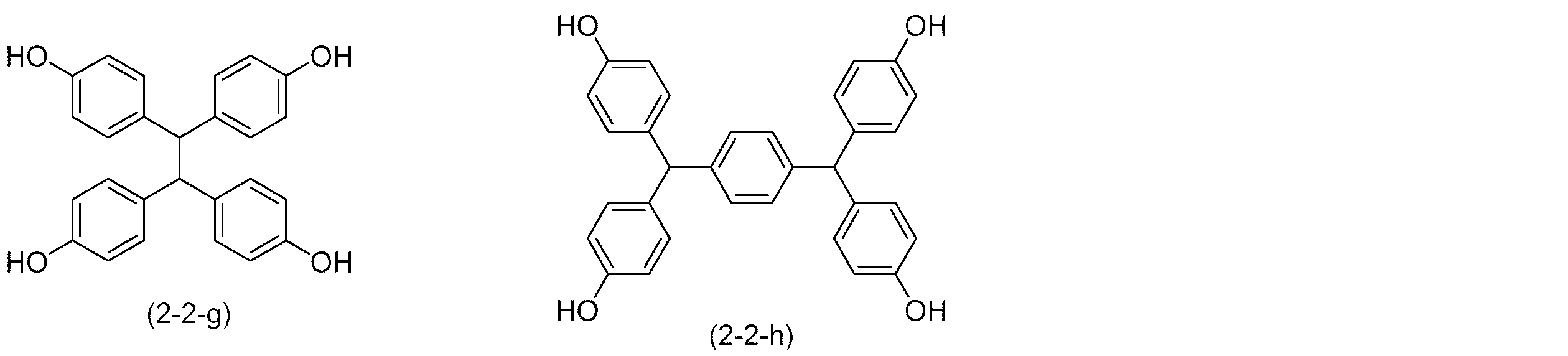
前記(B)化合物が、下記式(4-1)で表されてもよい:
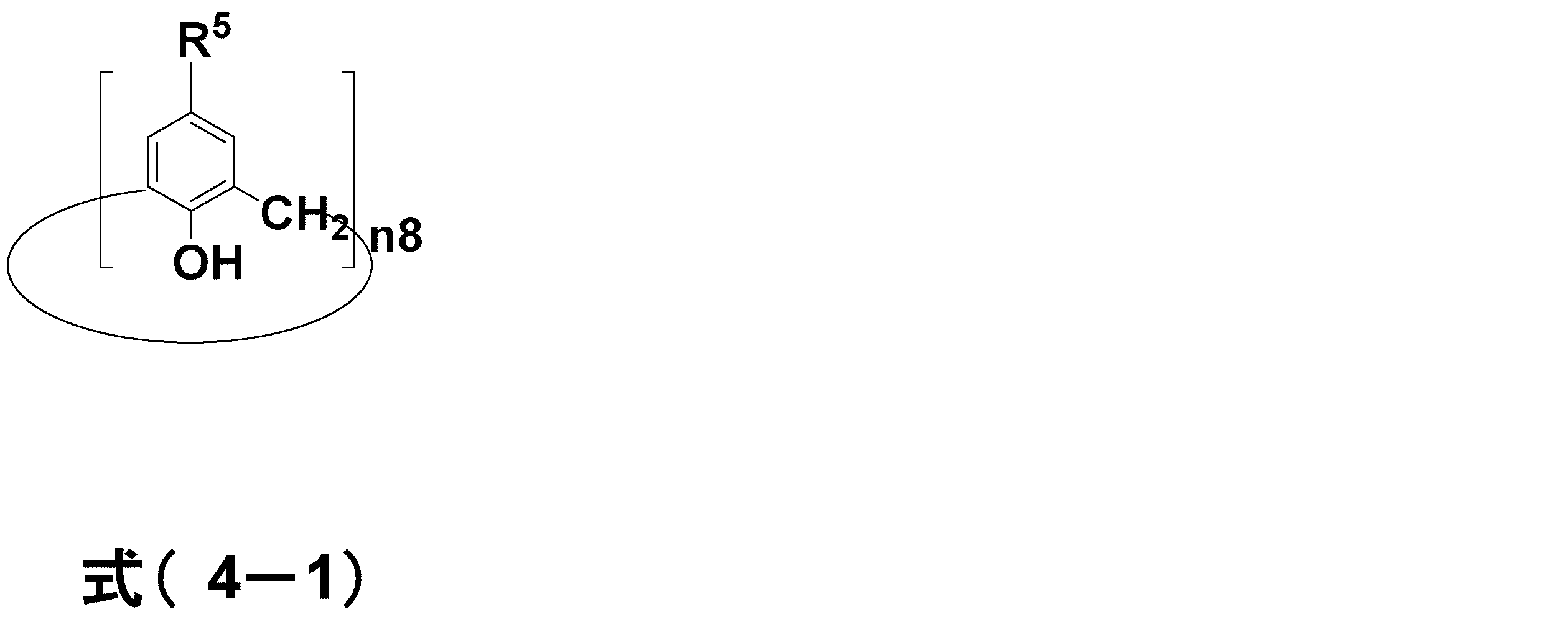
(式中、R5はハロゲノ基、カルボキシ基、ニトロ基、シアノ基、メチレンジオキシ基、アセトキシ基、メチルチオ基、炭素原子数1~9のアルコキシ基、炭素原子数1~3のアルキル基で置換されていてもよいアミノ基、ヒドロキシ基又はハロゲノ基で置換されていてもよい炭素原子数1~10のアルキル基を表す。式中、n8は4、5、6、8の整数を表す。)
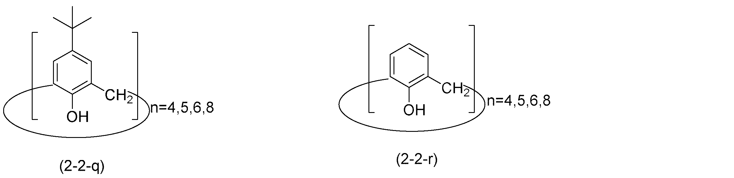
上記用語の説明は、前述の通りである。
式(4-1)で表させる化合物の具体例を以下に示す。
前記(B)化合物が、下記式(5-1)及び式(5-1-a)であってよい:
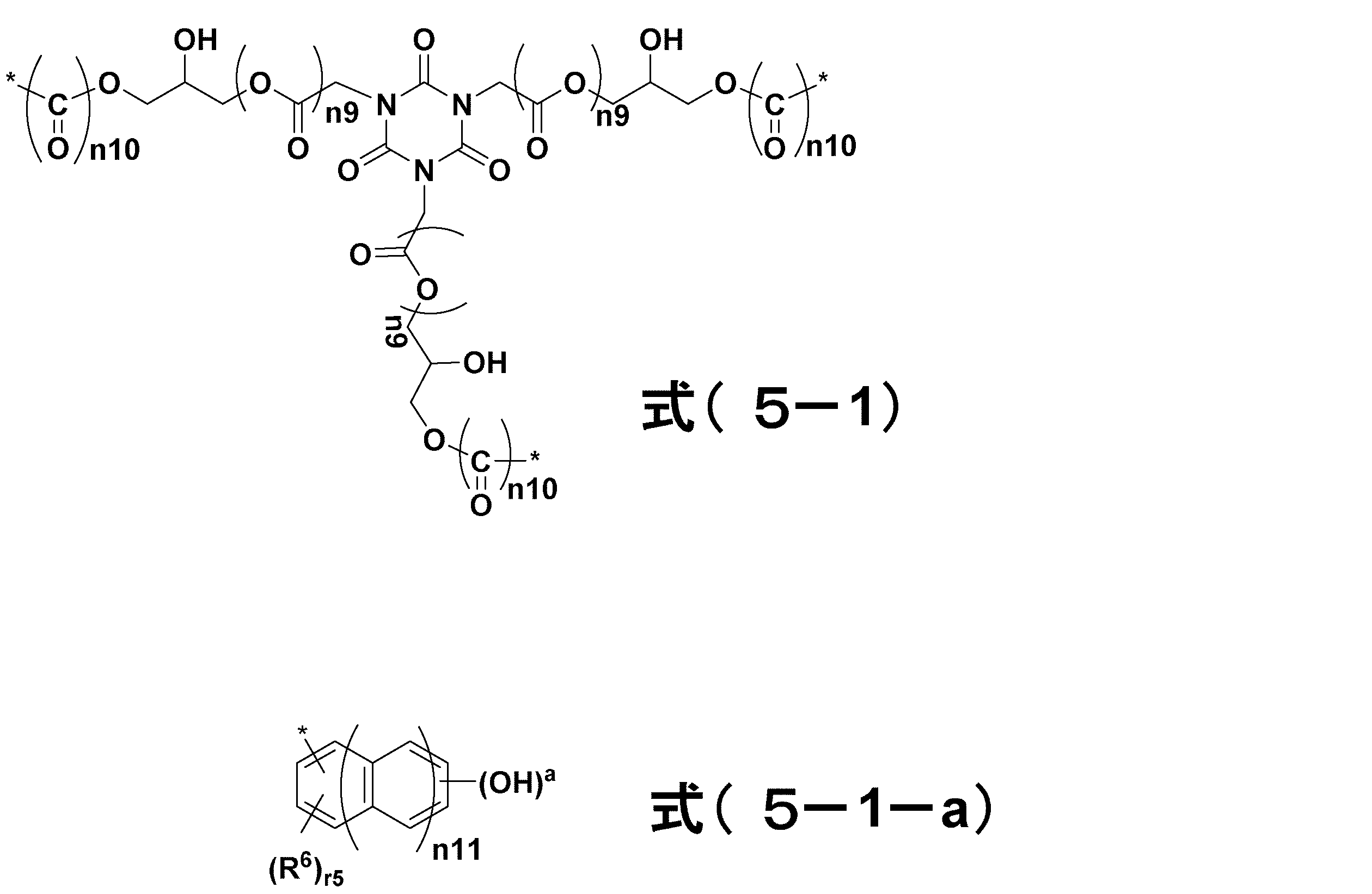
(式中、n9及びn10はそれぞれ0又は1の整数を表し、R6はハロゲノ基、カルボキシ基、ニトロ基、シアノ基、メチレンジオキシ基、アセトキシ基、メチルチオ基、炭素原子数1~9のアルコキシ基、炭素原子数1~3のアルキル基で置換されていてもよいアミノ基、ヒドロキシ基又はハロゲノ基で置換されていてもよい炭素原子数1~10のアルキル基を表す。aは1~6の整数を表す。n11は1又は2の整数を表す。r5は0~3の整数を表す。*は、式(5-1)の化合物と、式(5-1-a)の化合物との結合部位を表す。)
上記用語の説明は、前述の通りである。
下記式(5-1)及び式(5-1-a)で表される化合物の具体例を以下に示す。

前記(B)カテコール以外のフェノール性ヒドロキシ基を有する化合物は、下記に示す化合物であってよい。
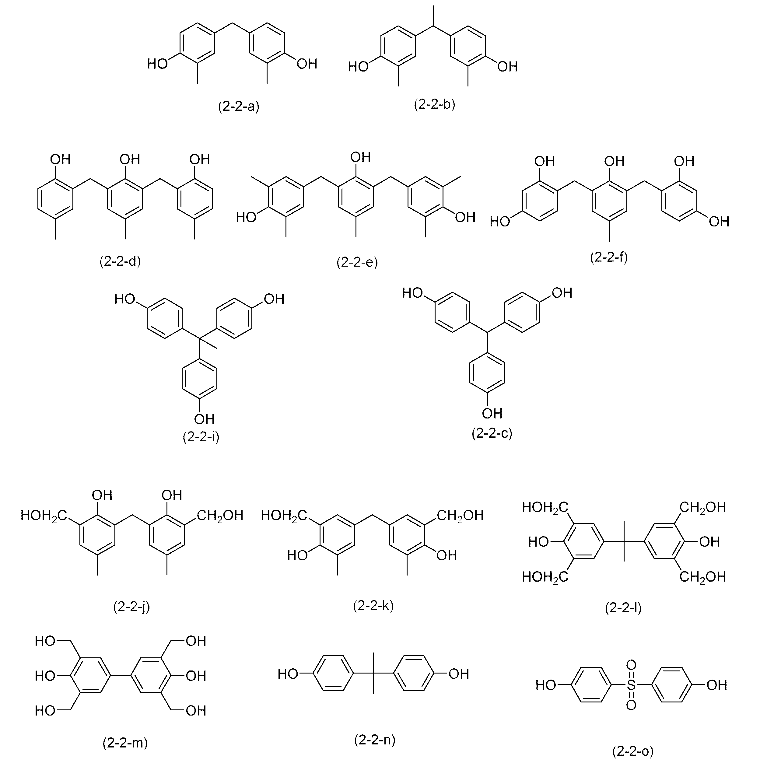
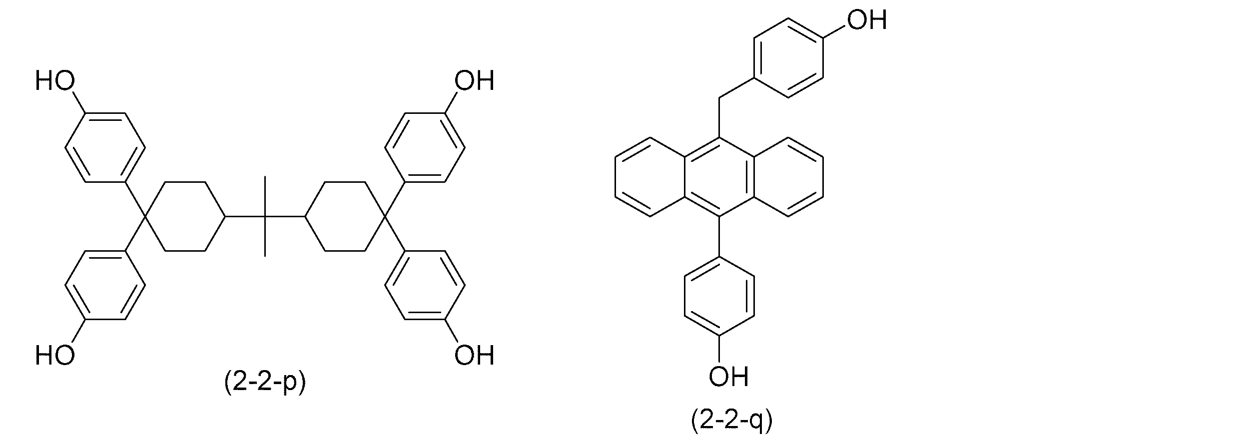
[3] カテコール以外のフェノール性ヒドロキシ基を有する重合体
前記カテコール以外のフェノール性ヒドロキシ基を有する化合物又は重合体(B)は、カテコール以外のフェノール性ヒドロキシ基を有する重合体(B)とすることができ、本願発明の効果を損ねない重合体であれば特に限定されない。
前記カテコール以外のフェノール性ヒドロキシ基を有する化合物又は重合体(B)は、カテコール以外のフェノール性ヒドロキシ基を有する重合体(B)とすることができ、本願発明の効果を損ねない重合体であれば特に限定されない。
前記(B)重合体は、好ましくは少なくとも3以上の繰り返し単位構造を有する。
前記(B)重合体の重量平均分子量は特に制限がないが、例えば1,000~50,000である。
前記(B)重合体が、下記式(3-1)で表される単位構造を含むことが好ましい:

(式中、T4はハロゲノ基で置換されていてもよい炭素原子数1~10のアルキル基を表す。R4はハロゲノ基、カルボキシ基、ニトロ基、シアノ基、メチレンジオキシ基、アセトキシ基、メチルチオ基、炭素原子数1~9のアルコキシ基、炭素原子数1~3のアルキル基で置換されていてもよいアミノ基、ヒドロキシ基又はハロゲノ基で置換されていてもよい炭素原子数1~10のアルキル基を表す。r4は0~3の整数を表す。n7は0~2の整数を表す。aは1~6の整数を表す。)
前記ハロゲノ基、アルキル基及びアルコキシ基の説明は上述の通りである。
(式中、T4はハロゲノ基で置換されていてもよい炭素原子数1~10のアルキル基を表す。R4はハロゲノ基、カルボキシ基、ニトロ基、シアノ基、メチレンジオキシ基、アセトキシ基、メチルチオ基、炭素原子数1~9のアルコキシ基、炭素原子数1~3のアルキル基で置換されていてもよいアミノ基、ヒドロキシ基又はハロゲノ基で置換されていてもよい炭素原子数1~10のアルキル基を表す。r4は0~3の整数を表す。n7は0~2の整数を表す。aは1~6の整数を表す。)
前記ハロゲノ基、アルキル基及びアルコキシ基の説明は上述の通りである。
前記式(3-1)で表させる重合体は、式(3-1)で表される単位構造を1種含む重合体でもよく、2種以上含む共重合体であってよい。
前記式(3-1)で表される(B)重合体の具体例としては、以下に記載の単位構造を含む重合体が挙げられる。

<熱酸発生剤>
本願の保護膜形成組成物は、熱酸発生剤をさらに含んでもよい。
本願の保護膜形成組成物は、熱酸発生剤をさらに含んでもよい。
熱酸発生剤としては、例えば、ピリジニウム-p-トルエンスルホナート、ピリジニウム-トリフルオロメタンスルホナート、ピリニジウム-p-フェノールスルホナート、K-PURE〔登録商標〕CXC-1612、同CXC-1614、同TAG-2172、同TAG-2179、同TAG-2678、同TAG2689(以上、King Industries社製)、及びSI-45、SI-60、SI-80、SI-100、SI-110、SI-150(以上、三新化学工業株式会社製)が挙げられる。
これら熱酸発生剤は、1種又は2種以上を組み合わせて用いることができる。
本願の保護膜形成組成物が熱酸発生剤を含む場合、その含有量は、保護膜形成組成物の全固形分に対して、0.0001~20質量%、好ましくは0.01~15質量%、さらに好ましくは0.1~10質量%である。
<溶剤>
本発明の保護膜形成組成物は、前記各成分を、溶剤、好ましくは有機溶剤に溶解させることによって調製でき、均一な溶液状態で用いられる。
本発明の保護膜形成組成物は、前記各成分を、溶剤、好ましくは有機溶剤に溶解させることによって調製でき、均一な溶液状態で用いられる。
本発明に係る保護膜形成組成物の有機溶剤としては、前記化合物や、下記に記載の酸触媒等の固形成分を溶解できる有機溶剤であれば、特に制限なく使用することができる。特に、本発明に係る保護膜形成組成物は均一な溶液状態で用いられるものであるため、その塗布性能を考慮すると、リソグラフィー工程に一般的に使用される有機溶剤を併用することが推奨される。
前記有機溶剤としては、例えば、エチレングリコールモノメチルエーテル、エチレングリコールモノエチルエーテル、メチルセロソルブアセテート、エチルセロソルブアセテート、ジエチレングリコールモノメチルエーテル、ジエチレングリコールモノエチルエーテル、プロピレングリコール、プロピレングリコールモノメチルエーテル、プロピレングリコールモノエチルエーテル、プロピレングリコールモノメチルエーテルアセテート、プロピレングリコールプロピルエーテルアセテート、トルエン、キシレン、メチルエチルケトン、メチルイソブチルケトン、シクロペンタノン、シクロヘキサノン、シクロヘプタノン、4-メチル-2-ペンタノール、2―ヒドロキシイソ酪酸メチル、2―ヒドロキシイソ酪酸エチル、エトキシ酢酸エチル、酢酸2-ヒドロキシエチル、3-メトキシプロピオン酸メチル、3-メトキシプロピオン酸エチル、3-エトキシプロピオン酸エチル、3-エトキシプロピオン酸メチル、ピルビン酸メチル、ピルビン酸エチル、酢酸エチル、酢酸ブチル、乳酸エチル、乳酸ブチル、2-ヘプタノン、メトキシシクロペンタン、アニソール、γ-ブチロラクトン、N-メチルピロリドン、N,N-ジメチルホルムアミド、及びN,N-ジメチルアセトアミドが挙げられる。これらの溶剤は、単独で又は2種以上を組み合わせて用いることができる。
これらの溶媒の中でプロピレングリコールモノメチルエーテル、プロピレングリコールモノメチルエーテルアセテート、乳酸エチル、乳酸ブチル、及びシクロヘキサノン等が好ましい。特にプロピレングリコールモノメチルエーテル、プロピレングリコールモノメチルエーテルアセテートが好ましい。
本発明に係る保護膜形成組成物の固形分は通常0.1~70質量%、好ましくは0.1~60質量%とする。固形分は保護膜形成組成物から溶媒を除いた全成分の含有割合である。固形分中における前記式(1-1)で表される重合体の割合は、1~100質量%、1~99.9質量%、50~99.9質量%、50~95質量%、50~90質量%の順で好ましい。
<レジスト下層膜形成組成物>
本発明のレジスト下層膜形成組成物は、(A)下記式(1-1)で表される単位構造を有する重合体:
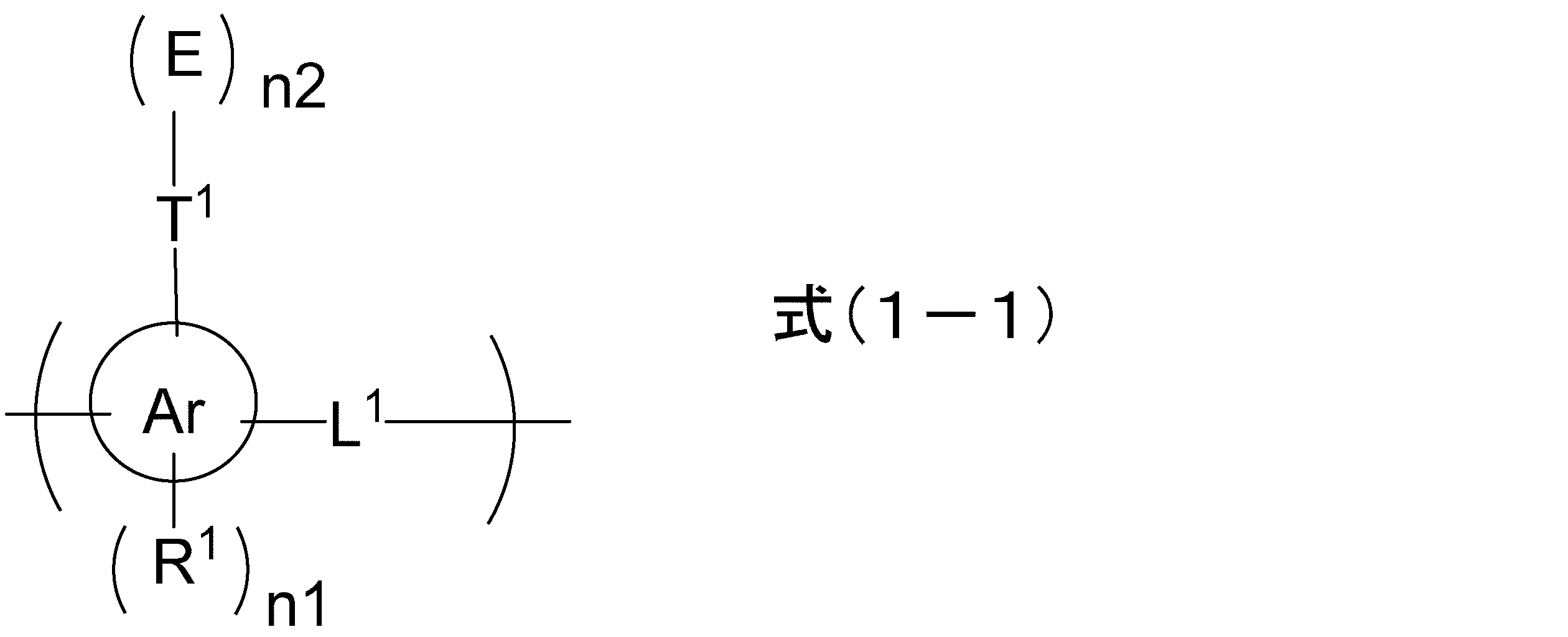
(式(1-1)中、Arはベンゼン環、ナフタレン環又はアントラセン環を表し、R1はヒドロキシ基、メチル基で保護されていてもよいメルカプト基、メチル基で保護されていてもよいアミノ基、ハロゲノ基又は、ヘテロ原子で置換若しくは中断されていてもよくヒドロキシ基で置換されていてもよい炭素原子数1~10のアルキル基を表し、n1は0~3の整数を表し、L1は単結合又は炭素原子数1~10のアルキレン基を表し、Eはエポキシ基を表し、T1はn2=1のとき、単結合又は、エーテル結合、エステル結合若しくはアミド結合で中断されていてもよい炭素原子数1~10のアルキレン基を表し、T1はn2=2のとき、窒素原子又はアミド結合を表す)、
(B)カテコール以外のフェノール性ヒドロキシ基を有する化合物又は重合体、
(C)熱酸発生剤、及び
(D)溶剤、
を含む。本願レジスト下層膜形成組成物に係る用語の説明は、前記保護膜形成組成物での説明内容と同一である。
本発明のレジスト下層膜形成組成物は、(A)下記式(1-1)で表される単位構造を有する重合体:
(式(1-1)中、Arはベンゼン環、ナフタレン環又はアントラセン環を表し、R1はヒドロキシ基、メチル基で保護されていてもよいメルカプト基、メチル基で保護されていてもよいアミノ基、ハロゲノ基又は、ヘテロ原子で置換若しくは中断されていてもよくヒドロキシ基で置換されていてもよい炭素原子数1~10のアルキル基を表し、n1は0~3の整数を表し、L1は単結合又は炭素原子数1~10のアルキレン基を表し、Eはエポキシ基を表し、T1はn2=1のとき、単結合又は、エーテル結合、エステル結合若しくはアミド結合で中断されていてもよい炭素原子数1~10のアルキレン基を表し、T1はn2=2のとき、窒素原子又はアミド結合を表す)、
(B)カテコール以外のフェノール性ヒドロキシ基を有する化合物又は重合体、
(C)熱酸発生剤、及び
(D)溶剤、
を含む。本願レジスト下層膜形成組成物に係る用語の説明は、前記保護膜形成組成物での説明内容と同一である。
<保護膜、レジスト下層膜、レジストパターン付き基板及び半導体装置の製造方法>
以下、本発明に係る保護膜形成組成物(レジスト下層膜形成組成物)を用いたレジストパターン付き基板の製造方法及び半導体装置の製造方法について説明する。
以下、本発明に係る保護膜形成組成物(レジスト下層膜形成組成物)を用いたレジストパターン付き基板の製造方法及び半導体装置の製造方法について説明する。
本発明に係るレジストパターン付き基板は、前記した保護膜形成組成物(レジスト下層膜形成組成物)を半導体基板上に塗布し、焼成することにより製造することができる。
本発明の保護膜形成組成物(レジスト下層膜形成組成物)が塗布される半導体基板としては、例えば、シリコンウエハ、ゲルマニウムウエハ、及びヒ化ガリウム、リン化インジウム、窒化ガリウム、窒化インジウム、窒化アルミニウム等の化合物半導体ウエハが挙げられる。
表面に無機膜が形成された半導体基板を用いる場合、当該無機膜は、例えば、ALD(原子層堆積)法、CVD(化学気相堆積)法、反応性スパッタ法、イオンプレーティング法、真空蒸着法、スピンコーティング法(スピンオングラス:SOG)により形成される。前記無機膜として、例えば、ポリシリコン膜、酸化ケイ素膜、窒化ケイ素膜、酸窒化ケイ素膜、BPSG(Boro-Phospho Silicate Glass)膜、窒化チタン膜、酸窒化チタン膜、窒化タングステン膜、窒化ガリウム膜、及びヒ化ガリウム膜が挙げられる。前記半導体基板は、いわゆるビア(穴)、トレンチ(溝)等が形成された段差基板であってもよい。例えばビアは、上面から見ると略円形の形状であり、略円の直径は例えば2nm~20nm、深さは50nm~500nm、トレンチは例えば溝(基板の凹部)の幅が2nm~20nm、深さは50nm~500nmである。本願の保護膜形成組成物(レジスト下層膜形成組成物)は組成物中に含まれる化合物の重量平均分子量及び平均粒径が小さいため、前記のような段差基板にも、ボイド(空隙)等の欠陥なく、該組成物を埋め込むことができる。半導体製造の次工程(半導体基板のウエットエッチング/ドライエッチング、レジストパターン形成)のために、ボイド等の欠陥が無いのは重要な特性である。
このような半導体基板上に、スピナー、コーター等の適当な塗布方法により本発明の保護膜形成組成物(レジスト下層膜形成組成物)を塗布する。その後、ホットプレート等の加熱手段を用いてベークすることにより保護膜(レジスト下層膜)を形成する。ベーク条件としては、ベーク温度100℃~400℃、ベーク時間0.3分~60分間の中から適宜、選択される。好ましくは、ベーク温度120℃~350℃、ベーク時間0.5分~30分間、より好ましくは、ベーク温度150℃~300℃、ベーク時間0.8分~10分間である。形成される保護膜の膜厚としては、例えば0.001μm~10μm、好ましくは0.002μm~1μm、より好ましくは0.005μm~0.5μmである。ベーク時の温度が、前記範囲より低い場合には架橋が不十分となり、形成される保護膜((レジスト下層膜形成組成物)の、レジスト溶剤又は塩基性過酸化水素水溶液に対する耐性が得られにくくなることがある。一方、ベーク時の温度が前記範囲より高い場合は、保護膜(レジスト下層膜)が熱によって分解してしまうことがある。
露光は、所定のパターンを形成するためのマスク(レチクル)を通して行われ、例えば、i線、KrFエキシマレーザー、ArFエキシマレーザー、EUV(極端紫外線)またはEB(電子線)が使用される。現像にはアルカリ現像液が用いられ、現像温度5℃~50℃、現像時間10秒~300秒から適宜選択される。アルカリ現像液としては、例えば、水酸化ナトリウム、水酸化カリウム、炭酸ナトリウム、ケイ酸ナトリウム、メタケイ酸ナトリウム、アンモニア水等の無機アルカリ類、エチルアミン、n-プロピルアミン等の第一アミン類、ジエチルアミン、ジ-n-ブチルアミン等の第二アミン類、トリエチルアミン、メチルジエチルアミン等の第三アミン類、ジメチルエタノールアミン、トリエタノールアミン等のアルコールアミン類、テトラメチルアンモニウムヒドロキシド、テトラエチルアンモニウムヒドロキシド、コリン等の第4級アンモニウム塩、ピロール、ピペリジン等の環状アミン類、等のアルカリ類の水溶液を使用することができる。さらに、前記アルカリ類の水溶液にイソプロピルアルコール等のアルコール類、ノニオン系等の界面活性剤を適当量添加して使用することもできる。これらの中で好ましい現像液は第四級アンモニウム塩、さらに好ましくはテトラメチルアンモニウムヒドロキシド及びコリンである。さらに、これらの現像液に界面活性剤などを加えることもできる。アルカリ現像液に代えて、酢酸ブチル等の有機溶媒で現像を行い、フォトレジストのアルカリ溶解速度が向上していない部分を現像する方法を用いることもできる。
次いで、形成したレジストパターンをマスクとして、前記保護膜(レジスト下層膜形成組成物)をドライエッチングする。その際、用いた半導体基板の表面に前記無機膜が形成されている場合、その無機膜の表面を露出させ、用いた半導体基板の表面に前記無機膜が形成されていない場合、その半導体基板の表面を露出させる。
さらに、ドライエッチング後の保護膜(レジスト下層膜形成組成物)(その保護膜/レジスト下層膜上にレジストパターンが残存している場合、そのレジストパターンも)をマスクとして、半導体用ウエットエッチング液を用いてウエットエッチングすることにより、所望のパターンが形成される。
半導体用ウエットエッチング液としては、半導体用ウエハをエッチング加工するための一般的な薬液を使用することが出来、例えば酸性を示す物質、塩基性を示す物質何れも使用することができる。
酸性を示す物質としては、例えば過酸化水素、フッ酸、フッ化アンモニウム、酸性フッ化アンモニウム、フッ化水素アンモニウム、バッファードフッ酸、塩酸、硝酸、硫酸、リン酸又はこれらの混合液が挙げられる。
塩基性を示す物質としては、アンモニア、水酸化ナトリウム、水酸化カリウム、シアン化ナトリウム、シアン化カリウム、トリエタノールアミン等の有機アミンと過酸化水素水とを混合し、pHを塩基性にした、塩基性過酸化水素水を挙げることができる。具体例としては、SC-1(アンモニア-過酸化水素溶液)が挙げられる。その他、pHを塩基性にすることができるもの、例えば、尿素と過酸化水素水を混合し、加熱により尿素の熱分解を引き起こすことでアンモニアを発生させ、最終的にpHを塩基性にするものも、ウエットエッチングの薬液として使用できる。
これらの中でも、酸性過酸化水素水又は塩基性過酸化水素水であることが好ましい。
これらの薬液は、界面活性剤等の添加剤が含まれていてもよい。
半導体用ウエットエッチング液の使用温度は25℃~90℃であることが望ましく、40℃~80℃であることがさらに望ましい。ウエットエッチング時間としては、0.5分~30分であることが望ましく、1分~20分であることがさらに望ましい。
次に実施例を挙げ本発明の内容を具体的に説明するが、本発明はこれらに限定されるものではない。
本明細書の下記合成例1~合成例8に示す化合物の重量平均分子量は、ゲルパーミエーションクロマトグラフィー(以下、GPCと略称する)による測定結果である。測定には東ソー(株)製GPC装置を用い、測定条件等は次のとおりである。
GPCカラム:Shodex KF803L、Shodex KF802、Shodex KF801〔登録商標〕(昭和電工(株))
カラム温度:40℃
溶媒:テトラヒドロフラン(THF)
流量:1.0ml/分
標準試料:ポリスチレン(東ソー(株)製)
カラム温度:40℃
溶媒:テトラヒドロフラン(THF)
流量:1.0ml/分
標準試料:ポリスチレン(東ソー(株)製)
<用語の説明>
PGME:プロピレングリコールモノメチルエーテル
PGMEA:プロピレングリコールモノメチルエーテルアセテート
PGME:プロピレングリコールモノメチルエーテル
PGMEA:プロピレングリコールモノメチルエーテルアセテート
<実施例1>
エポキシノボラック樹脂EOCN-104S(日本化薬(株)製品、式(a‐1)に相当)5.92g(30質量%PGMEA溶液、重量平均分子量は3,100)にTrisP-HAP(本州化学工業(株)製品、式(a‐2)に相当)5.91g(6質量%PGME溶液)、熱酸発生剤としてK-PURE〔商標登録〕TAG-2689(King Industries社製品)3.55g(0.5質量%PGME溶液)、R-40-LM(DIC(株))(1質量%PGMEA溶液)0.18g、PGMEA29.18gおよびPGME5.26gを混合し、固形分4.3質量%溶液とした。その溶液を、孔径0.2μmのポリテトラフルオロエチレン製ミクロフィルタを用いてろ過して、保護膜形成組成物を調製した。
エポキシノボラック樹脂EOCN-104S(日本化薬(株)製品、式(a‐1)に相当)5.92g(30質量%PGMEA溶液、重量平均分子量は3,100)にTrisP-HAP(本州化学工業(株)製品、式(a‐2)に相当)5.91g(6質量%PGME溶液)、熱酸発生剤としてK-PURE〔商標登録〕TAG-2689(King Industries社製品)3.55g(0.5質量%PGME溶液)、R-40-LM(DIC(株))(1質量%PGMEA溶液)0.18g、PGMEA29.18gおよびPGME5.26gを混合し、固形分4.3質量%溶液とした。その溶液を、孔径0.2μmのポリテトラフルオロエチレン製ミクロフィルタを用いてろ過して、保護膜形成組成物を調製した。


<実施例2>
エポキシノボラック樹脂EOCN-104S(日本化薬(株)製品、式(a‐1)に相当)5.32g(30質量%PGMEA溶液、重量平均分子量は3,100)にTrisP-HAP(本州化学工業(株)製品、式(a‐2)に相当)10.63g(6質量%PGME溶液)、熱酸発生剤としてK-PURE〔商標登録〕TAG-2689(King Industries社製品)3.19g(0.5質量%PGME溶液)、R-40-LM(DIC(株))(1質量%PGMEA溶液)0.18g、PGMEA29.55gおよびPGME1.16gを混合し、固形分4.5質量%溶液とした。その溶液を、孔径0.2μmのポリテトラフルオロエチレン製ミクロフィルタを用いてろ過して、保護膜形成組成物を調製した。
エポキシノボラック樹脂EOCN-104S(日本化薬(株)製品、式(a‐1)に相当)5.32g(30質量%PGMEA溶液、重量平均分子量は3,100)にTrisP-HAP(本州化学工業(株)製品、式(a‐2)に相当)10.63g(6質量%PGME溶液)、熱酸発生剤としてK-PURE〔商標登録〕TAG-2689(King Industries社製品)3.19g(0.5質量%PGME溶液)、R-40-LM(DIC(株))(1質量%PGMEA溶液)0.18g、PGMEA29.55gおよびPGME1.16gを混合し、固形分4.5質量%溶液とした。その溶液を、孔径0.2μmのポリテトラフルオロエチレン製ミクロフィルタを用いてろ過して、保護膜形成組成物を調製した。


<実施例3>
エポキシノボラック樹脂EOCN-104S(日本化薬(株)製品、式(a‐1)に相当)2.40g(30質量%PGMEA溶液、重量平均分子量は3,100)にVP-8000(日本曹達(株)製品、式(a‐3)に相当、重量平均分子量は10,257)0.24g(30質量%PGMEA溶液)、熱酸発生剤としてK-PURE〔商標登録〕TAG-2689(King Industries社製品)0.72g(1質量%PGME溶液)、R-40-LM(DIC(株))(1質量%PGMEA溶液)0.072g、PGMEA11.52gおよびPGME5.05gを混合し、固形分4.0質量%溶液とした。その溶液を、孔径0.2μmのポリテトラフルオロエチレン製ミクロフィルタを用いてろ過して、保護膜形成組成物を調製した。
エポキシノボラック樹脂EOCN-104S(日本化薬(株)製品、式(a‐1)に相当)2.40g(30質量%PGMEA溶液、重量平均分子量は3,100)にVP-8000(日本曹達(株)製品、式(a‐3)に相当、重量平均分子量は10,257)0.24g(30質量%PGMEA溶液)、熱酸発生剤としてK-PURE〔商標登録〕TAG-2689(King Industries社製品)0.72g(1質量%PGME溶液)、R-40-LM(DIC(株))(1質量%PGMEA溶液)0.072g、PGMEA11.52gおよびPGME5.05gを混合し、固形分4.0質量%溶液とした。その溶液を、孔径0.2μmのポリテトラフルオロエチレン製ミクロフィルタを用いてろ過して、保護膜形成組成物を調製した。


<実施例4>
エポキシノボラック樹脂EOCN-104S(日本化薬(株)製品、式(a-1)に相当)2.03g(30質量%PGMEA溶液、重量平均分子量は3,100)にVP-8000(日本曹達(株)製品、式(a‐3)に相当、重量平均分子量は10,257)0.61g(30質量%PGMEA溶液)、熱酸発生剤としてK-PURE〔商標登録〕TAG-2689(King Industries社製品)0.61g(1質量%PGME溶液)、R-40-LM(DIC(株))(1質量%PGMEA溶液)0.061g、PGMEA11.53gおよびPGME5.16gを混合し、固形分4.0質量%溶液とした。その溶液を、孔径0.2μmのポリテトラフルオロエチレン製ミクロフィルタを用いてろ過して、保護膜形成組成物を調製した。
エポキシノボラック樹脂EOCN-104S(日本化薬(株)製品、式(a-1)に相当)2.03g(30質量%PGMEA溶液、重量平均分子量は3,100)にVP-8000(日本曹達(株)製品、式(a‐3)に相当、重量平均分子量は10,257)0.61g(30質量%PGMEA溶液)、熱酸発生剤としてK-PURE〔商標登録〕TAG-2689(King Industries社製品)0.61g(1質量%PGME溶液)、R-40-LM(DIC(株))(1質量%PGMEA溶液)0.061g、PGMEA11.53gおよびPGME5.16gを混合し、固形分4.0質量%溶液とした。その溶液を、孔径0.2μmのポリテトラフルオロエチレン製ミクロフィルタを用いてろ過して、保護膜形成組成物を調製した。


<実施例5>
エポキシノボラック樹脂EOCN-104S(日本化薬(株)製品、式(a-1)に相当)3.60g(30質量%PGMEA溶液、重量平均分子量は3,100)にTEP-DF(旭有機材(株)製品、式(a‐4)に相当)2.70g(4質量%PGME溶液)、熱酸発生剤としてK-PURE〔商標登録〕TAG-2689(King Industries社製品)1.08g(1質量%PGME溶液)、R-40-LM(DIC(株))(1質量%PGMEA溶液)0.11g、PGMEA17.53gおよびPGME4.98gを混合し、固形分4.0質量%溶液とした。その溶液を、孔径0.2μmのポリテトラフルオロエチレン製ミクロフィルタを用いてろ過して、保護膜形成組成物を調製した。
エポキシノボラック樹脂EOCN-104S(日本化薬(株)製品、式(a-1)に相当)3.60g(30質量%PGMEA溶液、重量平均分子量は3,100)にTEP-DF(旭有機材(株)製品、式(a‐4)に相当)2.70g(4質量%PGME溶液)、熱酸発生剤としてK-PURE〔商標登録〕TAG-2689(King Industries社製品)1.08g(1質量%PGME溶液)、R-40-LM(DIC(株))(1質量%PGMEA溶液)0.11g、PGMEA17.53gおよびPGME4.98gを混合し、固形分4.0質量%溶液とした。その溶液を、孔径0.2μmのポリテトラフルオロエチレン製ミクロフィルタを用いてろ過して、保護膜形成組成物を調製した。


<実施例6>
エポキシノボラック樹脂EOCN-104S(日本化薬(株)製品、式(a-1)に相当)3.05g(30質量%PGMEA溶液、重量平均分子量は3,100)にTEP-DF(旭有機材(株)製品、式(a‐4)に相当)6.87g(4質量%PGME溶液)、熱酸発生剤としてK-PURE〔商標登録〕TAG-2689(King Industries社製品)0.92g(1質量%PGME溶液)、R-40-LM(DIC(株))(1質量%PGMEA溶液)0.092g、PGMEA17.93gおよびPGME1.14gを混合し、固形分4.0質量%溶液とした。その溶液を、孔径0.2μmのポリテトラフルオロエチレン製ミクロフィルタを用いてろ過して、保護膜形成組成物を調製した。
エポキシノボラック樹脂EOCN-104S(日本化薬(株)製品、式(a-1)に相当)3.05g(30質量%PGMEA溶液、重量平均分子量は3,100)にTEP-DF(旭有機材(株)製品、式(a‐4)に相当)6.87g(4質量%PGME溶液)、熱酸発生剤としてK-PURE〔商標登録〕TAG-2689(King Industries社製品)0.92g(1質量%PGME溶液)、R-40-LM(DIC(株))(1質量%PGMEA溶液)0.092g、PGMEA17.93gおよびPGME1.14gを混合し、固形分4.0質量%溶液とした。その溶液を、孔径0.2μmのポリテトラフルオロエチレン製ミクロフィルタを用いてろ過して、保護膜形成組成物を調製した。


<実施例7>
エポキシノボラック樹脂EOCN-104S(日本化薬(株)製品、式(a-1)に相当)3.60g(30質量%PGMEA溶液、重量平均分子量は3,100)にTEP-TPA(旭有機材(株)製品、式(a‐5)に相当)2.70g(4質量%PGME溶液)、熱酸発生剤としてK-PURE〔商標登録〕TAG-2689(King Industries社製品)1.08g(1質量%PGME溶液)、R-40-LM(DIC(株))(1質量%PGMEA溶液)0.108g、PGMEA17.53gおよびPGME4.98gを混合し、固形分4.0質量%溶液とした。その溶液を、孔径0.2μmのポリテトラフルオロエチレン製ミクロフィルタを用いてろ過して、保護膜形成組成物を調製した。
エポキシノボラック樹脂EOCN-104S(日本化薬(株)製品、式(a-1)に相当)3.60g(30質量%PGMEA溶液、重量平均分子量は3,100)にTEP-TPA(旭有機材(株)製品、式(a‐5)に相当)2.70g(4質量%PGME溶液)、熱酸発生剤としてK-PURE〔商標登録〕TAG-2689(King Industries社製品)1.08g(1質量%PGME溶液)、R-40-LM(DIC(株))(1質量%PGMEA溶液)0.108g、PGMEA17.53gおよびPGME4.98gを混合し、固形分4.0質量%溶液とした。その溶液を、孔径0.2μmのポリテトラフルオロエチレン製ミクロフィルタを用いてろ過して、保護膜形成組成物を調製した。

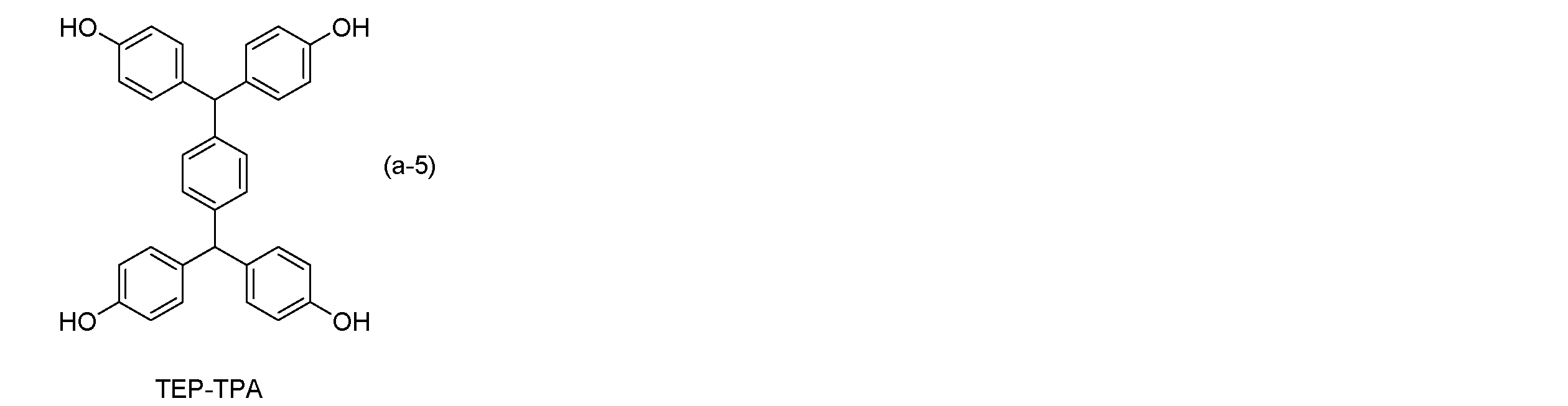
<実施例8>
エポキシノボラック樹脂EOCN-104S(日本化薬(株)製品、式(a-1)に相当)3.05g(30質量%PGMEA溶液、重量平均分子量は3,100)にTEP-TPA(旭有機材(株)製品、式(a‐5)に相当)6.87g(4質量%PGME溶液)、熱酸発生剤としてK-PURE〔商標登録〕TAG-2689(King Industries社製品)0.92g(1質量%PGME溶液)、R-40-LM(DIC(株))(1質量%PGMEA溶液)0.092g、PGMEA17.93gおよびPGME1.14gを混合し、固形分4.0質量%溶液とした。その溶液を、孔径0.2μmのポリテトラフルオロエチレン製ミクロフィルタを用いてろ過して、保護膜形成組成物を調製した。
エポキシノボラック樹脂EOCN-104S(日本化薬(株)製品、式(a-1)に相当)3.05g(30質量%PGMEA溶液、重量平均分子量は3,100)にTEP-TPA(旭有機材(株)製品、式(a‐5)に相当)6.87g(4質量%PGME溶液)、熱酸発生剤としてK-PURE〔商標登録〕TAG-2689(King Industries社製品)0.92g(1質量%PGME溶液)、R-40-LM(DIC(株))(1質量%PGMEA溶液)0.092g、PGMEA17.93gおよびPGME1.14gを混合し、固形分4.0質量%溶液とした。その溶液を、孔径0.2μmのポリテトラフルオロエチレン製ミクロフィルタを用いてろ過して、保護膜形成組成物を調製した。

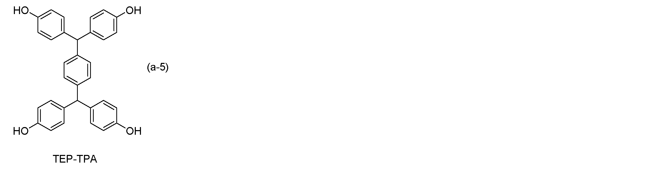
<実施例9>
エポキシノボラック樹脂EOCN-104S(日本化薬(株)製品、式(a-1)に相当)2.40g(30質量%PGMEA溶液、重量平均分子量は3,100)にNM8280G(旭有機材(株)製品、式(a‐6)に相当、重量平均分子量は6,819)0.24g(30質量%PGMEA溶液)、熱酸発生剤としてK-PURE〔商標登録〕TAG-2689(King Industries社製品)0.72g(1質量%PGME溶液)、R-40-LM(DIC(株))(1質量%PGMEA溶液)0.072g、PGMEA11.52gおよびPGME5.05gを混合し、固形分4.0質量%溶液とした。その溶液を、孔径0.2μmのポリテトラフルオロエチレン製ミクロフィルタを用いてろ過して、保護膜形成組成物を調製した。
エポキシノボラック樹脂EOCN-104S(日本化薬(株)製品、式(a-1)に相当)2.40g(30質量%PGMEA溶液、重量平均分子量は3,100)にNM8280G(旭有機材(株)製品、式(a‐6)に相当、重量平均分子量は6,819)0.24g(30質量%PGMEA溶液)、熱酸発生剤としてK-PURE〔商標登録〕TAG-2689(King Industries社製品)0.72g(1質量%PGME溶液)、R-40-LM(DIC(株))(1質量%PGMEA溶液)0.072g、PGMEA11.52gおよびPGME5.05gを混合し、固形分4.0質量%溶液とした。その溶液を、孔径0.2μmのポリテトラフルオロエチレン製ミクロフィルタを用いてろ過して、保護膜形成組成物を調製した。


<実施例10>
エポキシノボラック樹脂EOCN-104S(日本化薬(株)製品、式(a-1)に相当)2.03g(30質量%PGMEA溶液、重量平均分子量は3,100)にNM8280G(旭有機材(株)製品、式(a‐6)に相当、重量平均分子量は6,819)0.60g(30質量%PGMEA溶液)、熱酸発生剤としてK-PURE〔商標登録〕TAG-2689(King Industries社製品)0.61g(1質量%PGME溶液)、R-40-LM(DIC(株))(1質量%PGMEA溶液)0.061g、PGMEA11.53gおよびPGME5.76gを混合し、固形分4.0質量%溶液とした。その溶液を、孔径0.2μmのポリテトラフルオロエチレン製ミクロフィルタを用いてろ過して、保護膜形成組成物を調製した。
エポキシノボラック樹脂EOCN-104S(日本化薬(株)製品、式(a-1)に相当)2.03g(30質量%PGMEA溶液、重量平均分子量は3,100)にNM8280G(旭有機材(株)製品、式(a‐6)に相当、重量平均分子量は6,819)0.60g(30質量%PGMEA溶液)、熱酸発生剤としてK-PURE〔商標登録〕TAG-2689(King Industries社製品)0.61g(1質量%PGME溶液)、R-40-LM(DIC(株))(1質量%PGMEA溶液)0.061g、PGMEA11.53gおよびPGME5.76gを混合し、固形分4.0質量%溶液とした。その溶液を、孔径0.2μmのポリテトラフルオロエチレン製ミクロフィルタを用いてろ過して、保護膜形成組成物を調製した。


<比較例1>
エポキシノボラック樹脂EOCN-104S(日本化薬(株)製品、式(a‐1)に相当))7.46g(30質量%PGMEA溶液、重量平均分子量は3,100)、熱酸発生剤としてK-PURE〔商標登録〕TAG-2689(King Industries社製品)2.68g(0.5質量%PGME溶液)、PGMEA28.21gおよびPGME11.65gを混合し、固形分4.5質量%溶液とした。その溶液を、孔径0.2μmのポリテトラフルオロエチレン製ミクロフィルタを用いてろ過して、保護膜形成組成物を調製した。
エポキシノボラック樹脂EOCN-104S(日本化薬(株)製品、式(a‐1)に相当))7.46g(30質量%PGMEA溶液、重量平均分子量は3,100)、熱酸発生剤としてK-PURE〔商標登録〕TAG-2689(King Industries社製品)2.68g(0.5質量%PGME溶液)、PGMEA28.21gおよびPGME11.65gを混合し、固形分4.5質量%溶液とした。その溶液を、孔径0.2μmのポリテトラフルオロエチレン製ミクロフィルタを用いてろ過して、保護膜形成組成物を調製した。

(塗膜の形成)
窒化チタン膜が表面に形成されたシリコン基板上に、実施例1~実施例10で調製した保護膜形成組成物及び比較例1で調製した膜形成組成物の各々をスピンコートにて塗布し、250℃で60秒ベークすることで、100nmの膜厚の塗膜を作製した。
窒化チタン膜が表面に形成されたシリコン基板上に、実施例1~実施例10で調製した保護膜形成組成物及び比較例1で調製した膜形成組成物の各々をスピンコートにて塗布し、250℃で60秒ベークすることで、100nmの膜厚の塗膜を作製した。
(塩基性過酸化水素水溶液への耐性試験)
実施例1~実施例10で調製した保護膜形成組成物及び比較例1で調製した保護膜形成組成物の各々を用いて窒化チタン膜が表面に形成されたシリコン基板上に作製した塗膜を、下記表1で示した組成の塩基性過酸化水素水溶液に、同表に示す温度で浸し、その後水洗、乾燥後の塗膜の状態を目視で観察した。その結果を下記表2に示す。表2中の数値は比較例を基準に剥がれが観察された時間の比率を表記した。
実施例1~実施例10で調製した保護膜形成組成物及び比較例1で調製した保護膜形成組成物の各々を用いて窒化チタン膜が表面に形成されたシリコン基板上に作製した塗膜を、下記表1で示した組成の塩基性過酸化水素水溶液に、同表に示す温度で浸し、その後水洗、乾燥後の塗膜の状態を目視で観察した。その結果を下記表2に示す。表2中の数値は比較例を基準に剥がれが観察された時間の比率を表記した。
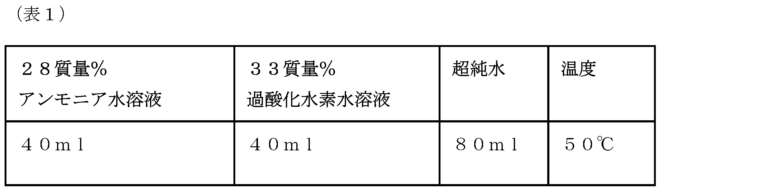
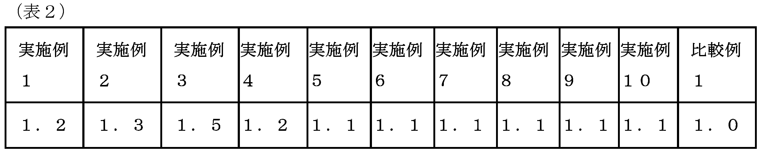
上記表2の結果より、実施例1~実施例10で調製した保護膜形成組成物を用いて作製した塗膜は、比較例1と比較して、塩基性過酸化水素水溶液に対して耐性が向上することがわかった。
(光学パラメーターの試験)
本明細書に記載の実施例1~10及び比較例1で調製された保護膜形成組成物を、それぞれスピナーによりシリコンウエハー上に塗布した。ホットプレート上、250℃で1分間ベークし、レジスト下層膜(膜厚50nm)を形成した。そして、これらの膜について分光エリプソメーター(J.A.Woollam社、VUV-VASE VU-302)を用い、波長193nm及び波長248nmでのn値(屈折率)及びk値(減衰係数又は吸光係数)を測定した。その結果を表3に示す。
本明細書に記載の実施例1~10及び比較例1で調製された保護膜形成組成物を、それぞれスピナーによりシリコンウエハー上に塗布した。ホットプレート上、250℃で1分間ベークし、レジスト下層膜(膜厚50nm)を形成した。そして、これらの膜について分光エリプソメーター(J.A.Woollam社、VUV-VASE VU-302)を用い、波長193nm及び波長248nmでのn値(屈折率)及びk値(減衰係数又は吸光係数)を測定した。その結果を表3に示す。
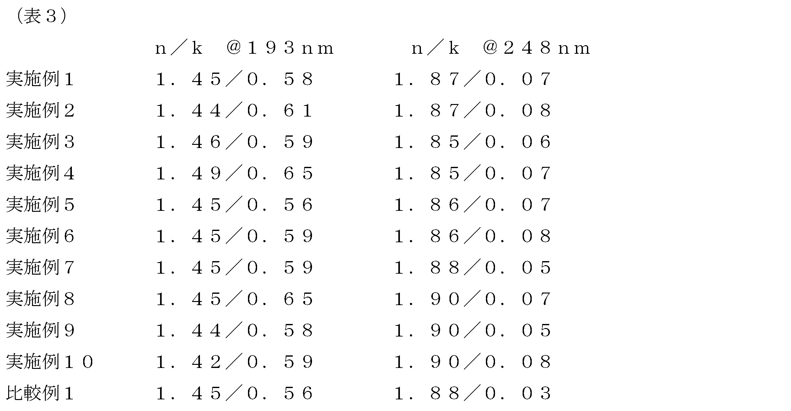
本発明に係る保護膜形成組成物は、基板加工にウエットエッチング液を適用する際に耐性に優れ、低ドライエッチング速度を有するため、基板加工の際の保護膜へのダメージが低い保護膜を提供するものである。本発明に係るレジスト下層膜形成組成物は、基板加工にウエットエッチング液を適用する際に耐性に優れ、低ドライエッチング速度を有し、且つ基板加工にウエットエッチング液を適用する際に耐性に優れる。
Claims (13)
- (A)下記式(1-1)で表される単位構造を有する重合体:
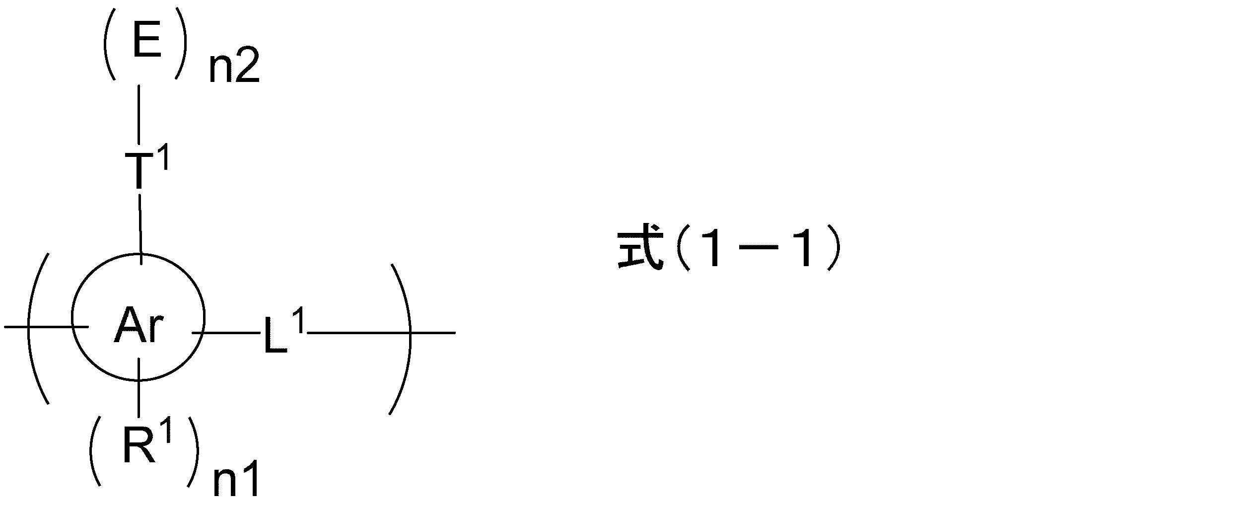
(式(1-1)中、Arはベンゼン環、ナフタレン環又はアントラセン環を表し、R1はヒドロキシ基、メチル基で保護されていてもよいメルカプト基、メチル基で保護されていてもよいアミノ基、ハロゲノ基又は、ヘテロ原子で置換若しくは中断されていてもよくヒドロキシ基で置換されていてもよい炭素原子数1~10のアルキル基を表し、n1は0~3の整数を表し、L1は単結合又は炭素原子数1~10のアルキレン基を表し、Eはエポキシ基を表し、T1はn2=1のとき、単結合又は、エーテル結合、エステル結合若しくはアミド結合で中断されていてもよい炭素原子数1~10のアルキレン基を表し、T1はn2=2のとき、窒素原子又はアミド結合を表す)、
(B)カテコール以外のフェノール性ヒドロキシ基を有する化合物又は重合体、
(C)熱酸発生剤、及び
(D)溶剤、
を含む、半導体用ウエットエッチング液に対する保護膜形成組成物。 - 前記(B)化合物又は重合体が、2以上のフェノール性ヒドロキシ基を有する、請求項1に記載の保護膜形成組成物。
- 前記(B)化合物又は重合体が、下記式(2-1)で表される、請求項1又は2に記載の保護膜形成組成物:

(式中、R2及びT2は各々独立して、ハロゲノ基、カルボキシ基、ニトロ基、シアノ基、メチレンジオキシ基、アセトキシ基、メチルチオ基、炭素原子数1~9のアルコキシ基、炭素原子数1~3のアルキル基で置換されていてもよいアミノ基、ヒドロキシ基又はハロゲノ基で置換されていてもよい炭素原子数1~10のアルキル基を表す。A1とA2は各々独立して、炭素原子数1~10のアルキレン基、ビシクロ環化合物由来の2価の有機基、ビフェニレン基又は-CT2T3-で表される2価の有機基又はそれらの組み合わせであり、T3は水素原子又は(式2-1-a)で表される1価の基を表す:
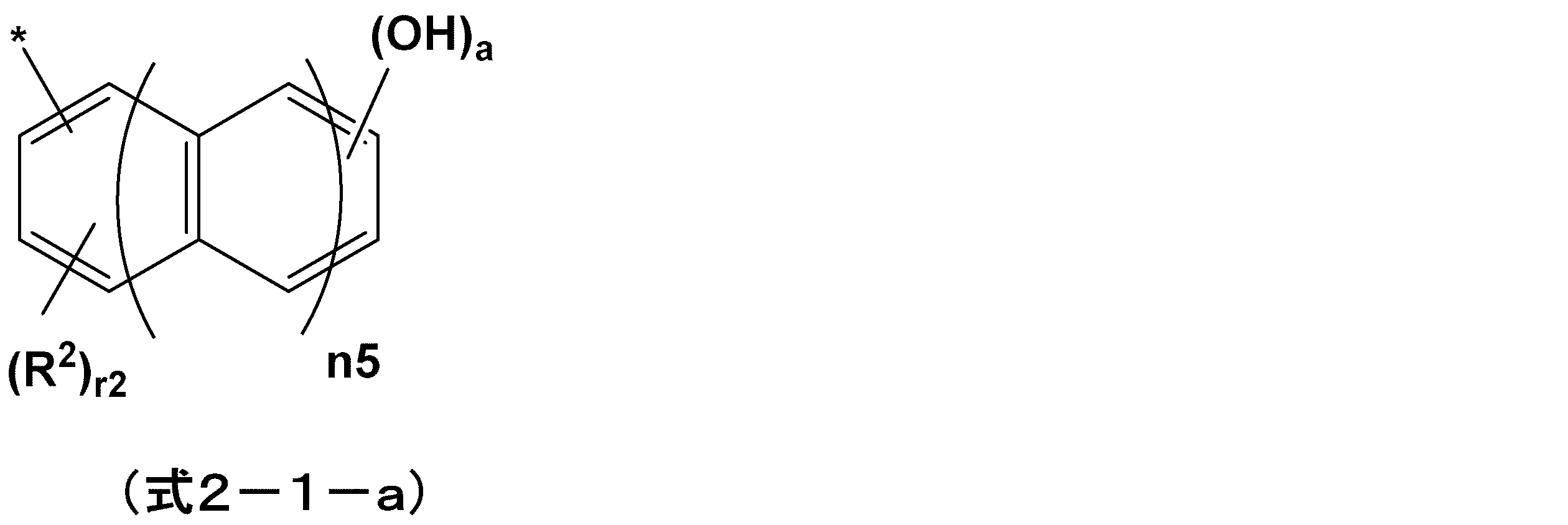
(式2-1-a)中の*は、T3が結合する炭素原子との結合部位を表す。aは1~6の整数を表す。
n3~n5は各々独立して0~2の整数を表す。r2は0~3の整数を表す。m1とm2は各々独立して0~10,000,000の数を表す。) - 前記m1、n3~n5及びr2が0であり、m2が1である、請求項3に記載の保護膜形成組成物。
- 前記(B)化合物又は重合体が、下記式(2-2)で表される化合物である、請求項1又は2に記載の保護膜形成組成物:

(式中、R3はハロゲノ基、カルボキシ基、ニトロ基、シアノ基、メチレンジオキシ基、アセトキシ基、メチルチオ基、炭素原子数1~9のアルコキシ基、炭素原子数1~3のアルキル基で置換されていてもよいアミノ基、ヒドロキシ基又はハロゲノ基で置換されていてもよい炭素原子数1~10のアルキル基を表す。Q1は単結合、酸素原子、硫黄原子、スルホニル基、カルボニル基、イミノ基、炭素原子数6~40のアリーレン基、ハロゲノ基で置換されていてもよい炭素原子数1~10のアルキレン基を表す。aは1~6の整数を表す。n6は0~2の整数を表す。r3は0~3の整数を表す。) - 前記(B)化合物又は重合体が、下記式(3-1)で表される単位構造を含む重合体である、請求項1又は2に記載の保護膜形成組成物:
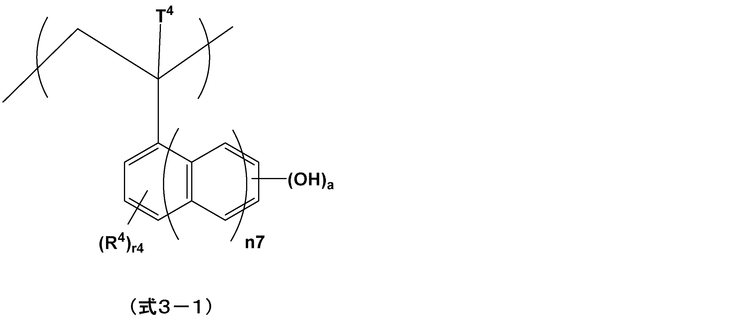
(式中、T4はハロゲノ基で置換されていてもよい炭素原子数1~10のアルキル基を表す。R4はハロゲノ基、カルボキシ基、ニトロ基、シアノ基、メチレンジオキシ基、アセトキシ基、メチルチオ基、炭素原子数1~9のアルコキシ基、炭素原子数1~3のアルキル基で置換されていてもよいアミノ基、ヒドロキシ基又はハロゲノ基で置換されていてもよい炭素原子数1~10のアルキル基を表す。r4は0~3の整数を表す。n7は0~2の整数を表す。aは1~6の整数を表す。) - 請求項1~6のいずれか1項に記載の保護膜形成組成物からなる塗布膜の焼成物であることを特徴とする半導体用ウエットエッチング液に対する保護膜。
- (A)下記式(1-1)で表される単位構造を有する重合体:

(式(1-1)中、Arはベンゼン環、ナフタレン環又はアントラセン環を表し、R1はヒドロキシ基、メチル基で保護されていてもよいメルカプト基、メチル基で保護されていてもよいアミノ基、ハロゲノ基又は、ヘテロ原子で置換若しくは中断されていてもよくヒドロキシ基で置換されていてもよい炭素原子数1~10のアルキル基を表し、n1は0~3の整数を表し、L1は単結合又は炭素原子数1~10のアルキレン基を表し、Eはエポキシ基を表し、T1はn2=1のとき、単結合又は、エーテル結合、エステル結合若しくはアミド結合で中断されていてもよい炭素原子数1~10のアルキレン基を表し、T1はn2=2のとき、窒素原子又はアミド結合を表す)、
(B)カテコール以外のフェノール性ヒドロキシ基を有する化合物又は重合体、
(C)熱酸発生剤、及び
(D)溶剤、
を含む、レジスト下層膜形成組成物。 - 請求項8に記載のレジスト下層膜形成組成物からなる塗布膜の焼成物であることを特徴とするレジスト下層膜。
- 請求項1~6のいずれか1項に記載の保護膜形成組成物を、段差を有する半導体基板上に塗布し焼成して保護膜を形成する工程を含む、半導体の製造に用いることを特徴とする保護膜付き基板の製造方法。
- 請求項1~6のいずれか1項に記載の保護膜組成物又は請求項8に記載のレジスト下層膜形成組成物を半導体基板上に塗布し焼成してレジスト下層膜としての保護膜を形成する工程、該保護膜上にレジスト膜を形成し、次いで露光、現像してレジストパターンを形成する工程を含み、半導体の製造に用いることを特徴とするレジストパターン付き基板の製造方法。
- 表面に無機膜が形成されていてもよい半導体基板上に、請求項1~6のいずれか1項に記載の保護膜形成組成物を用いて保護膜を形成し、前記保護膜上にレジストパターンを形成し、前記レジストパターンをマスクとして前記保護膜をドライエッチングし、前記無機膜又は前記半導体基板の表面を露出させ、ドライエッチング後の前記保護膜をマスクとして、半導体用ウエットエッチング液を用いて前記無機膜又は前記半導体基板をウエットエッチング及び洗浄する工程を含む半導体装置の製造方法。
- 表面に無機膜が形成されていてもよい半導体基板上に、請求項8に記載のレジスト下層膜形成組成物を用いてレジスト下層膜を形成し、前記レジスト下層膜上にレジストパターンを形成し、前記レジストパターンをマスクとして前記レジスト下層膜をドライエッチングし、前記無機膜又は前記半導体基板の表面を露出させ、ドライエッチング後の前記レジスト下層膜をマスクとして、前記無機膜又は前記半導体基板をエッチングする工程を含む半導体装置の製造方法。
Priority Applications (4)
| Application Number | Priority Date | Filing Date | Title |
|---|---|---|---|
| CN202180061886.9A CN116057103B (zh) | 2020-09-10 | 2021-09-09 | 药液耐性保护膜 |
| JP2022547634A JP7841430B2 (ja) | 2020-09-10 | 2021-09-09 | 薬液耐性保護膜 |
| KR1020237008506A KR20230066359A (ko) | 2020-09-10 | 2021-09-09 | 약액내성 보호막 |
| US18/025,336 US20230333470A1 (en) | 2020-09-10 | 2021-09-09 | Chemical-resistant protective film |
Applications Claiming Priority (2)
| Application Number | Priority Date | Filing Date | Title |
|---|---|---|---|
| JP2020151888 | 2020-09-10 | ||
| JP2020-151888 | 2020-09-10 |
Publications (1)
| Publication Number | Publication Date |
|---|---|
| WO2022054853A1 true WO2022054853A1 (ja) | 2022-03-17 |
Family
ID=80631552
Family Applications (1)
| Application Number | Title | Priority Date | Filing Date |
|---|---|---|---|
| PCT/JP2021/033084 Ceased WO2022054853A1 (ja) | 2020-09-10 | 2021-09-09 | 薬液耐性保護膜 |
Country Status (6)
| Country | Link |
|---|---|
| US (1) | US20230333470A1 (ja) |
| JP (1) | JP7841430B2 (ja) |
| KR (1) | KR20230066359A (ja) |
| CN (1) | CN116057103B (ja) |
| TW (1) | TW202225246A (ja) |
| WO (1) | WO2022054853A1 (ja) |
Cited By (2)
| Publication number | Priority date | Publication date | Assignee | Title |
|---|---|---|---|---|
| WO2023228662A1 (ja) * | 2022-05-24 | 2023-11-30 | 日産化学株式会社 | 薬液耐性保護膜 |
| WO2023228661A1 (ja) * | 2022-05-24 | 2023-11-30 | 日産化学株式会社 | 薬液耐性保護膜 |
Citations (5)
| Publication number | Priority date | Publication date | Assignee | Title |
|---|---|---|---|---|
| JP2008026600A (ja) * | 2006-07-21 | 2008-02-07 | Shin Etsu Chem Co Ltd | レジスト下層膜形成材料及びパターン形成方法 |
| JP2008039811A (ja) * | 2006-08-01 | 2008-02-21 | Shin Etsu Chem Co Ltd | レジスト下層膜材料並びにそれを用いたレジスト下層膜基板およびパターン形成方法 |
| WO2018203464A1 (ja) * | 2017-05-02 | 2018-11-08 | 日産化学株式会社 | 過酸化水素水溶液に対する保護膜形成組成物 |
| WO2020153278A1 (ja) * | 2019-01-21 | 2020-07-30 | 日産化学株式会社 | アセタール構造及びアミド構造を有する保護膜形成組成物 |
| WO2021200769A1 (ja) * | 2020-03-30 | 2021-10-07 | 日産化学株式会社 | 薬液耐性保護膜 |
Family Cites Families (4)
| Publication number | Priority date | Publication date | Assignee | Title |
|---|---|---|---|---|
| JPWO2008117619A1 (ja) * | 2007-03-26 | 2010-07-15 | Jsr株式会社 | 感光性絶縁樹脂組成物 |
| WO2017029935A1 (ja) * | 2015-08-18 | 2017-02-23 | Dic株式会社 | ノボラック型フェノール性水酸基含有樹脂及びレジスト膜 |
| JP7196389B2 (ja) * | 2016-08-10 | 2022-12-27 | Jsr株式会社 | 半導体用レジスト下層膜形成組成物、レジスト下層膜、レジスト下層膜の形成方法及びパターニング基板の製造方法 |
| JP6718406B2 (ja) | 2017-03-31 | 2020-07-08 | 信越化学工業株式会社 | レジスト下層膜材料、パターン形成方法、及びレジスト下層膜形成方法 |
-
2021
- 2021-09-09 US US18/025,336 patent/US20230333470A1/en active Pending
- 2021-09-09 WO PCT/JP2021/033084 patent/WO2022054853A1/ja not_active Ceased
- 2021-09-09 JP JP2022547634A patent/JP7841430B2/ja active Active
- 2021-09-09 KR KR1020237008506A patent/KR20230066359A/ko active Pending
- 2021-09-09 CN CN202180061886.9A patent/CN116057103B/zh active Active
- 2021-09-09 TW TW110133544A patent/TW202225246A/zh unknown
Patent Citations (5)
| Publication number | Priority date | Publication date | Assignee | Title |
|---|---|---|---|---|
| JP2008026600A (ja) * | 2006-07-21 | 2008-02-07 | Shin Etsu Chem Co Ltd | レジスト下層膜形成材料及びパターン形成方法 |
| JP2008039811A (ja) * | 2006-08-01 | 2008-02-21 | Shin Etsu Chem Co Ltd | レジスト下層膜材料並びにそれを用いたレジスト下層膜基板およびパターン形成方法 |
| WO2018203464A1 (ja) * | 2017-05-02 | 2018-11-08 | 日産化学株式会社 | 過酸化水素水溶液に対する保護膜形成組成物 |
| WO2020153278A1 (ja) * | 2019-01-21 | 2020-07-30 | 日産化学株式会社 | アセタール構造及びアミド構造を有する保護膜形成組成物 |
| WO2021200769A1 (ja) * | 2020-03-30 | 2021-10-07 | 日産化学株式会社 | 薬液耐性保護膜 |
Cited By (2)
| Publication number | Priority date | Publication date | Assignee | Title |
|---|---|---|---|---|
| WO2023228662A1 (ja) * | 2022-05-24 | 2023-11-30 | 日産化学株式会社 | 薬液耐性保護膜 |
| WO2023228661A1 (ja) * | 2022-05-24 | 2023-11-30 | 日産化学株式会社 | 薬液耐性保護膜 |
Also Published As
| Publication number | Publication date |
|---|---|
| TW202225246A (zh) | 2022-07-01 |
| CN116057103A (zh) | 2023-05-02 |
| JPWO2022054853A1 (ja) | 2022-03-17 |
| KR20230066359A (ko) | 2023-05-15 |
| CN116057103B (zh) | 2026-04-10 |
| JP7841430B2 (ja) | 2026-04-07 |
| US20230333470A1 (en) | 2023-10-19 |
Similar Documents
| Publication | Publication Date | Title |
|---|---|---|
| JP6497527B2 (ja) | レジストパターン被覆用塗布液 | |
| EP2650729A1 (en) | Composition for forming resist underlayer film containing hydroxyl group-containing carbazole novolac resin | |
| TWI844674B (zh) | 包含脂環式化合物末端之聚合物的阻劑下層膜形成組成物、經圖型化之基板的製造方法、及半導體裝置之製造方法 | |
| JP7841430B2 (ja) | 薬液耐性保護膜 | |
| WO2022186231A1 (ja) | ベンジリデンシアノ酢酸エステル基を有するレジスト下層膜形成組成物 | |
| KR102800934B1 (ko) | 약액 내성 보호막 | |
| CN120936952A (zh) | 耐化学液性保护膜 | |
| WO2023100506A1 (ja) | ヒドロキシケイ皮酸誘導体を有するレジスト下層膜形成用組成物 | |
| US20250034427A1 (en) | Chemical-resistant protective film-forming composition having catechol group | |
| WO2021251481A1 (ja) | ジオール構造を含む保護膜形成用組成物 | |
| JP7859567B2 (ja) | 薬液耐性保護膜 | |
| WO2023084961A1 (ja) | 薬液耐性保護膜 | |
| TWI921328B (zh) | 半導體裝置的製造方法 | |
| TWI885249B (zh) | 含萘單元之阻劑下層膜形成組成物、經圖型化之基板之製造方法、半導體裝置之製造方法 | |
| WO2026083794A1 (ja) | レジスト下層膜形成用組成物 | |
| JP2020148891A (ja) | レジスト下層膜形成組成物 | |
| JP7244795B2 (ja) | 単分子層又は多分子層形成用組成物、単分子層又は多分子層及び積層体並びに基板の製造方法 | |
| WO2025183182A1 (ja) | 半導体素子形成用組成物 | |
| KR20250166879A (ko) | 레지스트 하층막 형성용 조성물 | |
| KR20250107863A (ko) | 쿠르쿠민 유도체를 갖는 레지스트 하층막 형성용 조성물 | |
| TW202613243A (zh) | 半導體裝置的製造方法 | |
| WO2023228662A1 (ja) | 薬液耐性保護膜 | |
| WO2023085295A1 (ja) | アルコキシ基含有レジスト下層膜形成用組成物 | |
| CN116783552A (zh) | 包含具有脂环式烃基的聚合物的抗蚀剂下层膜形成用组合物 |
Legal Events
| Date | Code | Title | Description |
|---|---|---|---|
| 121 | Ep: the epo has been informed by wipo that ep was designated in this application |
Ref document number: 21866811 Country of ref document: EP Kind code of ref document: A1 |
|
| ENP | Entry into the national phase |
Ref document number: 2022547634 Country of ref document: JP Kind code of ref document: A |
|
| NENP | Non-entry into the national phase |
Ref country code: DE |
|
| 122 | Ep: pct application non-entry in european phase |
Ref document number: 21866811 Country of ref document: EP Kind code of ref document: A1 |