WO2022054761A1 - 表示装置、発光装置および電子機器 - Google Patents
表示装置、発光装置および電子機器 Download PDFInfo
- Publication number
- WO2022054761A1 WO2022054761A1 PCT/JP2021/032684 JP2021032684W WO2022054761A1 WO 2022054761 A1 WO2022054761 A1 WO 2022054761A1 JP 2021032684 W JP2021032684 W JP 2021032684W WO 2022054761 A1 WO2022054761 A1 WO 2022054761A1
- Authority
- WO
- WIPO (PCT)
- Prior art keywords
- metal layer
- electrode
- layer
- display device
- light emitting
- Prior art date
- Legal status (The legal status is an assumption and is not a legal conclusion. Google has not performed a legal analysis and makes no representation as to the accuracy of the status listed.)
- Ceased
Links
Images







Classifications
-
- H—ELECTRICITY
- H10—SEMICONDUCTOR DEVICES; ELECTRIC SOLID-STATE DEVICES NOT OTHERWISE PROVIDED FOR
- H10K—ORGANIC ELECTRIC SOLID-STATE DEVICES
- H10K50/00—Organic light-emitting devices
- H10K50/80—Constructional details
- H10K50/805—Electrodes
- H10K50/81—Anodes
- H10K50/818—Reflective anodes, e.g. ITO combined with thick metallic layers
-
- G—PHYSICS
- G09—EDUCATION; CRYPTOGRAPHY; DISPLAY; ADVERTISING; SEALS
- G09F—DISPLAYING; ADVERTISING; SIGNS; LABELS OR NAME-PLATES; SEALS
- G09F9/00—Indicating arrangements for variable information in which the information is built-up on a support by selection or combination of individual elements
- G09F9/30—Indicating arrangements for variable information in which the information is built-up on a support by selection or combination of individual elements in which the desired character or characters are formed by combining individual elements
-
- H—ELECTRICITY
- H05—ELECTRIC TECHNIQUES NOT OTHERWISE PROVIDED FOR
- H05B—ELECTRIC HEATING; ELECTRIC LIGHT SOURCES NOT OTHERWISE PROVIDED FOR; CIRCUIT ARRANGEMENTS FOR ELECTRIC LIGHT SOURCES, IN GENERAL
- H05B33/00—Electroluminescent light sources
- H05B33/12—Light sources with substantially two-dimensional [2D] radiating surfaces
-
- H—ELECTRICITY
- H05—ELECTRIC TECHNIQUES NOT OTHERWISE PROVIDED FOR
- H05B—ELECTRIC HEATING; ELECTRIC LIGHT SOURCES NOT OTHERWISE PROVIDED FOR; CIRCUIT ARRANGEMENTS FOR ELECTRIC LIGHT SOURCES, IN GENERAL
- H05B33/00—Electroluminescent light sources
- H05B33/12—Light sources with substantially two-dimensional [2D] radiating surfaces
- H05B33/22—Light sources with substantially two-dimensional [2D] radiating surfaces characterised by the chemical or physical composition or the arrangement of auxiliary dielectric or reflective layers
-
- H—ELECTRICITY
- H05—ELECTRIC TECHNIQUES NOT OTHERWISE PROVIDED FOR
- H05B—ELECTRIC HEATING; ELECTRIC LIGHT SOURCES NOT OTHERWISE PROVIDED FOR; CIRCUIT ARRANGEMENTS FOR ELECTRIC LIGHT SOURCES, IN GENERAL
- H05B33/00—Electroluminescent light sources
- H05B33/12—Light sources with substantially two-dimensional [2D] radiating surfaces
- H05B33/26—Light sources with substantially two-dimensional [2D] radiating surfaces characterised by the composition or arrangement of the conductive material used as an electrode
-
- H—ELECTRICITY
- H10—SEMICONDUCTOR DEVICES; ELECTRIC SOLID-STATE DEVICES NOT OTHERWISE PROVIDED FOR
- H10K—ORGANIC ELECTRIC SOLID-STATE DEVICES
- H10K50/00—Organic light-emitting devices
- H10K50/80—Constructional details
- H10K50/805—Electrodes
- H10K50/81—Anodes
- H10K50/816—Multilayers, e.g. transparent multilayers
-
- H—ELECTRICITY
- H10—SEMICONDUCTOR DEVICES; ELECTRIC SOLID-STATE DEVICES NOT OTHERWISE PROVIDED FOR
- H10K—ORGANIC ELECTRIC SOLID-STATE DEVICES
- H10K59/00—Integrated devices, or assemblies of multiple devices, comprising at least one organic light-emitting element covered by group H10K50/00
- H10K59/80—Constructional details
- H10K59/805—Electrodes
- H10K59/8051—Anodes
- H10K59/80517—Multilayers, e.g. transparent multilayers
-
- H—ELECTRICITY
- H10—SEMICONDUCTOR DEVICES; ELECTRIC SOLID-STATE DEVICES NOT OTHERWISE PROVIDED FOR
- H10K—ORGANIC ELECTRIC SOLID-STATE DEVICES
- H10K59/00—Integrated devices, or assemblies of multiple devices, comprising at least one organic light-emitting element covered by group H10K50/00
- H10K59/80—Constructional details
- H10K59/805—Electrodes
- H10K59/8051—Anodes
- H10K59/80518—Reflective anodes, e.g. ITO combined with thick metallic layers
-
- H—ELECTRICITY
- H10—SEMICONDUCTOR DEVICES; ELECTRIC SOLID-STATE DEVICES NOT OTHERWISE PROVIDED FOR
- H10K—ORGANIC ELECTRIC SOLID-STATE DEVICES
- H10K2102/00—Constructional details relating to the organic devices covered by this subclass
- H10K2102/301—Details of OLEDs
- H10K2102/302—Details of OLEDs of OLED structures
- H10K2102/3023—Direction of light emission
- H10K2102/3026—Top emission
Definitions
- This disclosure relates to display devices, light emitting devices and electronic devices.
- organic EL (Electroluminescence) display devices (hereinafter simply referred to as “display devices”) have become widespread.
- This display device has a configuration in which an organic light emitting layer is provided between the first electrode and the second electrode.
- Various configurations have been proposed as the first electrode.
- Patent Document 1 discloses that the first electrode includes a metal layer and a transparent electrode, and the transparent electrode covers the main surface of the metal layer and the side surface of the metal layer. .. Further, the metal layer includes a first metal layer and a second metal layer, and the second metal layer is provided on the first metal layer, and the transparent electrode is sandwiched between the metal layer and the organic light emitting layer. Opposing ones are disclosed.
- Patent Document 1 when the one disclosed in Patent Document 1 is used as the first electrode, there is a problem that the reliability of the display device is lowered.
- An object of the present disclosure is to provide a display device, a light emitting device, and an electronic device capable of suppressing a decrease in reliability.
- the first disclosure is With multiple first electrodes, A second electrode facing a plurality of first electrodes, It is provided with an organic light emitting layer provided between a plurality of first electrodes and the second electrode.
- the first electrode is A metal layer having a main surface facing the organic light emitting layer, It covers the main surface of the metal layer and the sides of the metal layer, and is equipped with a transparent electrode containing a transparent conductive oxide.
- the metal layer is The first metal layer having hydrogen storage capacity and A second metal layer provided on the first metal layer and facing the organic light emitting layer with a transparent electrode interposed therebetween is provided.
- the peripheral edge of the first metal layer is a display device separated from the transparent electrode.
- the second disclosure is with the first electrode
- the second electrode facing the first electrode and It is provided with an organic light emitting layer provided between the first electrode and the second electrode.
- the first electrode is A metal layer having a main surface facing the organic light emitting layer, It covers the main surface of the metal layer and the sides of the metal layer, and is equipped with a transparent electrode containing a transparent conductive oxide.
- the metal layer is The first metal layer having hydrogen storage capacity and A second metal layer provided on the first metal layer and facing the organic light emitting layer with a transparent electrode interposed therebetween is provided.
- the peripheral edge of the first metal layer is a light emitting device separated from the transparent electrode.
- the third disclosure is an electronic device including the display device of the first disclosure or the light emitting device of the second disclosure.
- FIG. 1 is a schematic view showing an example of the overall configuration of the display device according to the first embodiment of the present disclosure.
- FIG. 2A is a cross-sectional view showing an example of the configuration of the display device according to the first embodiment of the present disclosure.
- FIG. 2B is a plan view showing an example of the configuration of the first electrode.
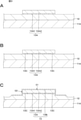
- 3A, 3B, and 3C are process diagrams for explaining an example of a method for manufacturing a display device according to the first embodiment of the present disclosure, respectively.
- 4A, 4C, and 4C are process diagrams for explaining an example of a method for manufacturing a display device according to the first embodiment of the present disclosure, respectively.
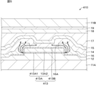
- FIG. 5 is a cross-sectional view showing the configuration of the display device according to the reference example.
- FIG. 6 is a cross-sectional view showing an example of the configuration of the display device according to the second embodiment of the present disclosure.
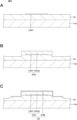
- 7A, 7B, and 7C are process diagrams for explaining an example of a method for manufacturing a display device according to a second embodiment of the present disclosure, respectively.
- FIG. 8 is a cross-sectional view showing an example of the configuration of the display device according to the third embodiment of the present disclosure.
- 9A, 9B, and 9C are process diagrams for explaining an example of a method for manufacturing a display device according to a third embodiment of the present disclosure, respectively.
- FIG. 10 is a cross-sectional view showing an example of the configuration of the display device according to the modified example of the first embodiment of the present disclosure.
- FIG. 10 is a cross-sectional view showing an example of the configuration of the display device according to the modified example of the first embodiment of the present disclosure.
- FIG. 11A is a diagram showing TDS spectra when the thermal desorption of water from samples 1-1 to 1-4 is measured.
- FIG. 11B is a diagram showing TDS spectra when the thermal desorption of hydrogen from samples 2-1 to 2-4 is measured.
- FIG. 12 is a plan view showing an example of the schematic configuration of the module.
- FIG. 13A is a front view showing an example of the appearance of a digital still camera.
- FIG. 13B is a rear view showing an example of the appearance of the digital still camera.
- FIG. 14 is a perspective view showing an example of the appearance of the head-mounted display.
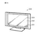
- FIG. 15 is a perspective view showing an example of the appearance of the television device.
- FIG. 1 is a schematic view showing an example of the overall configuration of the display device 10 according to the first embodiment of the present disclosure.
- the display device 10 has a display area 110A and a peripheral area 110B provided on the peripheral edge of the display area 110A.
- a plurality of sub-pixels 100R, 100G, and 100B are two-dimensionally arranged in a predetermined arrangement pattern such as a matrix.
- the pixel pitch of the sub-pixel 100 is preferably 10 ⁇ m or less from the viewpoint of increasing the definition of the display device 10.
- the sub-pixel 100R displays red
- the sub-pixel 100G displays green
- the sub-pixel 100B displays blue.
- the sub-pixels 100R, 100G, and 100B are not particularly distinguished, they are referred to as sub-pixel 100.
- a combination of adjacent sub-pixels 100R, 100G, and 100B constitutes one pixel.
- FIG. 1 shows an example in which a combination of three sub-pixels 100R, 100G, and 100B arranged in the row direction (horizontal direction) constitutes one pixel.
- the peripheral region 110B is provided with a signal line drive circuit 111 and a scanning line drive circuit 112, which are drivers for displaying images.
- the signal line drive circuit 111 supplies the signal voltage of the video signal corresponding to the luminance information supplied from the signal supply source (not shown) to the sub-pixel 100 selected via the signal line 111A.
- the scanning line drive circuit 112 is configured by a shift register or the like that sequentially shifts (transfers) the start pulse in synchronization with the input clock pulse.
- the scanning line drive circuit 112 scans the video signals in line units when writing the video signals to the sub-pixels 100, and sequentially supplies the scanning signals to the scanning lines 112A.
- the display device 10 is a microdisplay in which self-luminous elements such as an OLED or a Micro-OLED are formed in an array.
- the display device 10 is suitable for use in a display device for VR (Virtual Reality), MR (Mixed Reality) or AR (Augmented Reality), an electronic viewfinder (EVF), a small projector, or the like. be.
- FIG. 2A is a cross-sectional view showing an example of the configuration of the display device 10 according to the first embodiment of the present disclosure.
- the display device 10 includes a drive substrate 11A, a first insulating layer 12, a plurality of first electrodes 13, an organic layer 14, a second electrode 15, a second insulating layer 16, and a protective layer 17. , A color filter 18, a filled resin layer 19, and a facing substrate 11B are provided.
- the display device 10 is an example of a light emitting device.
- the display device 10 is a top emission type display device.
- the facing board 11B side is the top side
- the drive board 11A side is the bottom side.
- the surface on the top side of the display device 10 is referred to as a first surface
- the surface on the bottom side of the display device 10 is referred to as a second surface.
- the display device 10 includes a plurality of light emitting elements 10A.
- the light emitting element 10A is composed of a first electrode 13, an organic layer 14, and a second electrode 15.
- the light emitting element 10A is a white OLED or a white Micro-OLED (MOLED).
- a colorization method in the display device 10 a method using a white OLED and a color filter 18 is used. However, the colorization method is not limited to this, and an RGB coloring method or the like may be used.
- the drive board 11A is a so-called backplane and drives a plurality of light emitting elements 10A.
- a drive circuit including a sampling transistor and a drive transistor for controlling the drive of the plurality of light emitting elements 10A, and a power supply circuit for supplying power to the plurality of light emitting elements 10A (all). (Not shown) is provided.
- the drive substrate 11A may be made of, for example, glass or resin having low permeability of water and oxygen, or may be made of a semiconductor such as a transistor which can be easily formed.
- the drive substrate 11A may be a glass substrate, a semiconductor substrate, a resin substrate, or the like.
- the glass substrate includes, for example, high strain point glass, soda glass, borosilicate glass, forsterite, lead glass, quartz glass and the like.
- the semiconductor substrate includes, for example, amorphous silicon, polycrystalline silicon, single crystal silicon, and the like.
- the resin substrate contains, for example, at least one selected from the group consisting of polymethylmethacrylate, polyvinyl alcohol, polyvinylphenol, polyether sulfone, polyimide, polycarbonate, polyethylene terephthalate, polyethylene naphthalate and the like.
- the first insulating layer 12 is provided on the first surface of the drive board 11A and covers the drive circuit, the power supply circuit, and the like.
- the first insulating layer 12 includes a plurality of contact plugs (not shown) and wiring.
- the contact plug connects the light emitting element 10A to the drive circuit or wiring. Further, the contact plug connects the wiring and the drive circuit.
- the first insulating layer 12 is made of, for example, an organic material or an inorganic material.
- the organic material contains, for example, at least one selected from the group consisting of polyimide, acrylic resin and the like.
- the inorganic material includes, for example, at least one selected from the group consisting of silicon oxide, silicon nitride, silicon oxynitride, aluminum oxide and the like.
- the plurality of first electrodes 13 are provided on the first surface of the first insulating layer 12.
- the first electrode 13 is an anode.
- holes are injected from the first electrode 13 into the organic layer 14.
- the adjacent first electrode 13 is electrically separated.
- the first electrode 13 is connected to a contact plug provided in the first insulating layer 12.
- the first electrode 13 is connected to a drive circuit or wiring via this contact plug.
- FIG. 2B is a plan view showing an example of the configuration of the first electrode 13.
- the first electrode 13 includes a metal layer 13A and a transparent electrode 13B.
- the metal layer 13A has a function as a reflective layer that reflects the light emitted from the organic layer 14.
- the metal layer 13A has a first surface (main surface) S1 and a side surface S2, and the first surface S1 faces the organic layer 14.
- the metal layer 13A includes a first metal layer 13A1 and a second metal layer 13A2.
- the first metal layer 13A1 is provided between the first insulating layer 12 and the second metal layer 13A2.
- the first metal layer 13A1 improves the crystal orientation of the second metal layer 13A2 at the time of film formation of the second metal layer 13A2. Thereby, the uneven shape of the surface (first surface) of the second metal layer 13A2 can be reduced.
- the first metal layer 13A1 has a hydrogen storage capacity.
- the second surface of the first metal layer 13A1 is connected to a contact plug provided in the first insulating layer 12.
- the peripheral edge of the first metal layer 13A1 is separated from the transparent electrode 13B and is not in contact with the transparent electrode 13B. This makes it possible to suppress the generation of water due to the redox reaction between the first metal layer 13A1 and the transparent electrode 13B.
- the peripheral edge of the first metal layer 13A1 is located inside the peripheral edge of the second metal layer 13A2.
- a gap 13C is provided on the outside of the side surface of the first metal layer 13A1. More specifically, a gap 13C is provided between the peripheral edge of the second surface of the second metal layer 13A2 and the first surface of the first insulating layer 12.
- the peripheral edge portion of the second surface means a region having a predetermined width from the peripheral edge of the second surface toward the inside.
- An insulating layer or a metal layer may be provided in the gap 13C, or the gap 13C may be hollow.
- the hydrogen storage capacity of the insulating layer or the metal layer provided in the gap 13C is lower than the hydrogen storage capacity of the first metal layer 13A1. It is preferable that the insulating layer or the metal layer provided in the gap 13C does not have a hydrogen storage capacity.
- the constituent material of the insulating layer provided in the gap 13C may be the same as or different from the insulating material constituting the second insulating layer 16.
- the constituent material of the metal layer provided in the gap 13C may be the same as or different from that of the second metal layer 13A2.
- the first metal layer 13A1 contains at least one metal element selected from the group consisting of titanium (Ti) and tantalum (Ta).
- the first metal layer 13A1 may contain at least one of the above metal elements as a constituent element of the alloy.
- the second metal layer 13A2 is provided on the first surface of the first metal layer 13A1.
- the second metal layer 13A2 faces the organic layer 14 with the transparent electrode 13B interposed therebetween.
- the second metal layer 13A2 has a function as a reflective layer that reflects the light emitted from the organic layer 14.
- the hydrogen storage capacity of the second metal layer 13A2 is lower than that of the first metal layer 13A1.
- the second metal layer 13A2 preferably does not have a hydrogen storage capacity.
- the second metal layer 13A2 is, for example, aluminum (Al), silver (Ag), chromium (Cr), gold (Au), platinum (Pt), nickel (Ni), copper (Cu), molybdenum (Mo), and the like. It contains at least one metallic element selected from the group consisting of magnesium (Mg), iron (Fe) and tungsten (W).
- the second metal layer 13A2 may contain at least one of the above metal elements as a constituent element of the alloy. Specific examples of alloys include aluminum alloys and silver alloys. Specific examples of the aluminum alloy include, for example, AlNd or AlCu. From the viewpoint of improving the reflectance, the second metal layer 13A2 preferably contains at least one metal element selected from the group consisting of aluminum (Al) and silver (Ag) among the above metal elements. ..
- the transparent electrode 13B is provided on the first surface (main surface) S1 of the metal layer 13A and covers the first surface S1 of the metal layer 13A and the side surface S2 of the metal layer 13A.
- the transparent electrode 13B may be divided by the gap 13C.
- the work function of the transparent electrode 13B is preferably higher than that of the second metal layer 13A2. In this case, since the transparent electrode 13B is provided on the second metal layer 13A2, the hole injection property from the first electrode 13 to the organic layer 14 can be improved.
- the transparent electrode 13B preferably has a high transmittance from the viewpoint of improving the luminous efficiency.
- the transparent electrode 13B contains a transparent conductive oxide (TCO: Transparent Conductive Oxide).
- TCO Transparent Conductive Oxide
- the transparent conductive oxide is, for example, a transparent conductive oxide containing indium (hereinafter referred to as “indium-based transparent conductive oxide”) and a transparent conductive oxide containing tin (hereinafter referred to as “tin-based transparent conductive oxide”). ”) And a transparent conductive oxide containing zinc (hereinafter referred to as“ zinc-based transparent conductive oxide ”).
- the indium-based transparent conductive oxide includes, for example, indium tin oxide (ITO), indium tin oxide (IZO), indium gallium oxide (IGO) or indium gallium zinc oxide (IGZO) fluorine-doped indium oxide (IFO).
- ITO indium tin oxide
- ITO indium tin oxide
- Tin-based transparent conductive oxides include, for example, tin oxide, antimony-doped tin oxide (ATO) or fluorine-doped tin oxide (FTO).
- Zinc-based transparent conductive oxides include, for example, zinc oxide, aluminum-doped zinc oxide (AZO), boron-doped zinc oxide or gallium-doped zinc oxide (GZO).
- the second electrode 15 is provided so as to face the first electrode 13.
- the second electrode 15 is provided as an electrode common to all sub-pixels 100 in the display area 110A.
- the second electrode 15 is a cathode.
- the second electrode 15 is a transparent electrode having transparency to the light generated in the organic layer 14.
- the transparent electrode also includes a translucent reflective layer. It is preferable that the second electrode 15 is made of a material having as high a transparency as possible and a small work function in order to increase the luminous efficiency.
- the second electrode 15 is composed of, for example, at least one of a metal layer and a transparent electrode. More specifically, the second electrode 15 is composed of a metal layer or a single-layer film of a transparent electrode, or a laminated film of a metal layer and a transparent electrode.
- the metal layer may be provided on the organic layer 14 side or the transparent electrode may be provided on the organic layer 14 side, but it has a low work function. From the viewpoint of making the layer adjacent to the organic layer 14, it is preferable that the metal layer is provided on the organic layer 14 side.
- the metal layer contains, for example, at least one metal element selected from the group consisting of magnesium (Mg), aluminum (Al), silver (Ag), calcium (Ca) and sodium (Na).
- the metal layer may contain at least one of the above metal elements as a constituent element of the alloy. Specific examples of the alloy include MgAg alloy, MgAl alloy, AlLi alloy and the like.
- the transparent electrode contains a transparent conductive oxide. As the transparent conductive oxide, the same material as the above-mentioned transparent electrode 13B can be exemplified.
- the organic layer 14 is provided between the plurality of first electrodes 13 and the second electrodes 15.
- the organic layer 14 is provided as an organic layer common to all sub-pixels 100 in the display area 110A.
- the organic layer 14 is configured to be capable of emitting white light.
- the organic layer 14 has a structure in which a hole injection layer, a hole transport layer, a light emitting layer, and an electron transport layer are laminated in this order from the first electrode 13 toward the second electrode 15.
- the structure of the organic layer 14 is not limited to this, and layers other than the light emitting layer are provided as needed.
- the hole injection layer is a buffer layer for increasing the hole injection efficiency into the light emitting layer and for suppressing leakage.
- the hole transport layer is for increasing the hole transport efficiency to the light emitting layer. In the light emitting layer, when an electric field is applied, recombination of electrons and holes occurs, and light is generated.
- the light emitting layer is an organic light emitting layer containing an organic light emitting material.
- the electron transport layer is for increasing the electron transport efficiency to the light emitting layer.
- An electron injection layer may be provided between the electron transport layer and the second electrode 15. This electron injection layer is for increasing the electron injection efficiency.
- the second insulating layer 16 is provided on the first surface of the first insulating layer 12.
- the second insulating layer 16 is provided between the adjacent first electrodes 13 and electrically separates the adjacent first electrodes 13.
- the second insulating layer 16 has a plurality of openings 16A. Each of the plurality of openings 16A is provided corresponding to each sub-pixel 100.
- the opening 16A exposes the first surface of the first electrode 13 (the surface facing the second electrode 15).
- the first electrode 13 and the organic layer 14 come into contact with each other through the opening 16A.
- One opening 16A may be provided for one first electrode 13, or two openings 16A may be provided for one first electrode 13 (see FIG. 2B).
- the second insulating layer 16 may cover from the peripheral edge of the first surface of the first electrode 13 to the side surface (end surface) of the first electrode 13.
- the peripheral edge portion of the first surface means a region having a predetermined width from the peripheral edge of the first surface toward the inside.
- a part of the insulating material constituting the second insulating layer 16 may enter the gap 13C provided between the second insulating layer 16 and the second metal layer 13A2.
- the peripheral edge of the first metal layer 13A1 is preferably located outside the opening 16A of the second insulating layer 16. As a result, it is possible to prevent the crystal orientation of the portion of the second metal layer 13A2 corresponding to the opening 16A from being lowered. Therefore, of the first surface of the second metal layer 13A2, the uneven shape of the portion exposed from the opening 16A (that is, the portion of the first surface of the second metal layer 13A2 that comes into contact with the organic layer 14). Can be reduced.
- the same material as the above-mentioned first insulating layer 12 can be exemplified.
- the protective layer 17 is provided on the first surface of the second electrode 15 and covers the plurality of light emitting elements 10A.
- the protective layer 17 blocks the light emitting element 10A from the outside air and suppresses the infiltration of moisture from the external environment into the inside of the light emitting element 10A.
- the protective layer 17 may have a function of suppressing oxidation of the metal layer.
- the protective layer 17 is made of, for example, an inorganic material having low hygroscopicity.
- the inorganic material contains, for example, at least one of silicon oxide (SiO), silicon nitride (SiN), silicon nitride (SiNO), titanium oxide (TIO) and aluminum oxide (AlO).
- the protective layer 17 may have a single-layer structure, but may have a multi-layer structure when the thickness of the protective layer 17 is increased. This is to relieve the internal stress in the protective layer 17.
- the protective layer 17 may be made of a polymer resin.
- the polymer resin contains at least one selected from the group consisting of thermosetting resins, ultraviolet curable resins and the like.
- the color filter 18 is provided on the first surface of the protective layer 17.
- the color filter 18 is, for example, an on-chip color filter (OCCF).
- the color filter 18 includes, for example, a red filter, a green filter, and a blue filter.
- the red filter, the green filter, and the blue filter are provided facing the light emitting element 10A for the red sub-pixel 100R, the light emitting element 10A for the green sub pixel 100G, and the light emitting element 10A for the blue sub pixel 100B, respectively. There is. As a result, the sub-pixels 100R, 100G, and 100B are configured.
- the white light emitted from each of the light emitting elements 10A in the subpixels 100R, 100G, and 100B passes through the red filter, the green filter, and the blue filter, respectively, so that the red light, the green light, and the blue light are displayed on the display surface, respectively. Is emitted from. Further, a light-shielding layer (not shown) may be provided between the color filters of each color, that is, between the sub-pixels.
- the color filter 18 is not limited to the on-chip color filter, and may be provided on one main surface of the facing substrate 11B.
- the filling resin layer 19 is provided between the color filter 18 and the facing substrate 11B.
- the filled resin layer 19 has a function as an adhesive layer for adhering the color filter 18 and the facing substrate 11B.
- the packed resin layer 19 contains at least one selected from the group consisting of, for example, a thermosetting resin and an ultraviolet curable resin.
- the facing board 11B is provided so as to face the drive board 11A. More specifically, the opposed substrate 11B is provided so that the second surface of the opposed substrate 11B and the first surface of the drive substrate 11A face each other.
- the facing substrate 11B and the filled resin layer 19 seal the light emitting element 10A, the color filter 18, and the like.
- the facing substrate 11B is made of a material such as glass that is transparent to each color light emitted from the color filter 18.
- a drive circuit, a power supply circuit, and the like are formed on the first surface of the drive substrate 11A by using, for example, a thin film forming technique, a photolithography technique, and an etching technique.
- a first insulating layer 12 is formed on the first surface of the drive substrate 11A so as to cover the drive circuit, the power supply circuit, and the like.
- a plurality of contact plugs, a plurality of wirings, and the like are formed on the first insulating layer 12.
- the first metal layer 13A1 is formed on the first surface of the first insulating layer 12 by, for example, a sputtering method.
- a second metal layer 13A2 is formed on the first surface of the first metal layer 13A1 by a sputtering method.
- the first metal layer 13A1 and the second metal layer 13A2 are dry-etched via the resist mask.
- the first metal layer 13A1 and the second metal layer 13A2 are patterned by the above method (see FIG. 3A). As a result, the plurality of patterned metal layers 13A are formed on the first surface of the first insulating layer 12.
- the peripheral edge of the first metal layer 13A1 is retracted from the peripheral edge of the first metal layer 13A1 toward the center by, for example, wet etching.
- the peripheral edge of the first metal layer 13A1 is positioned inside the peripheral edge of the second metal layer 13A2, and the peripheral edge of the second surface of the second metal layer 13A2 is located.
- a gap 13C is formed between the portion and the first surface of the first insulating layer 12 (see FIG. 3B).
- the etching selectivity of the first metal layer 13A1 to the second metal layer 13A2 (etching rate of the first metal layer 13A1 / etching rate of the second metal layer 13A2) is large, and the first It is preferable to use a metal layer 13A1 that can be selectively etched.
- the chemical solution for wet etching one that does not corrode the second metal layer 13A2 is preferable.
- a transparent electrode 13B is formed on the first surface of the first insulating layer 12 so as to cover the plurality of metal layers 13A.
- the transparent electrode 13B may be divided by the gap 13C.
- the transparent electrode 13B has a structure that covers the entire metal layer 13A (that is, a structure that covers the side surface S2 of the metal layer 13A together with the first surface S1 of each metal layer 13A). As a result, it is possible to prevent each metal layer 13A from being dissolved in the developing solution when the resist mask of the transparent electrode 13B is formed.
- a resist mask having a predetermined pattern is formed on the first surface of the transparent electrode 13B, and then the transparent electrode 13B is dry-etched through the resist mask to pattern the transparent electrode 13B. As a result, a plurality of first electrodes 13 are formed on the first surface of the first insulating layer 12 (see FIG. 3C).
- a second insulating layer 16 is formed on the first surface of the first insulating layer 12 so as to cover the plurality of first electrodes 13. Then, a resist mask having a predetermined pattern is formed on the first surface of the second insulating layer 16, and then the second insulating layer 16 is etched through the resist mask to form a plurality of the second insulating layer 16.
- the opening 16A of the above is formed (see FIG. 4A).
- the hole injection layer, the hole transport layer, the light emitting layer, and the electron transport layer are placed on the first surface of the first electrode 13 and the first surface of the second insulating layer 16.
- the organic layer 14 is formed by laminating in order (see FIG. 4B).
- the second electrode 15 is formed on the first surface of the organic layer 14 by, for example, a thin film deposition method or a sputtering method. As a result, a plurality of light emitting elements 10A are formed on the first surface of the first insulating layer 12 (see FIG. 4C).
- the color filter 18 is placed on the first surface of the protective layer 17 by, for example, photolithography. Form.
- the flattening layer may be formed on both the upper, lower or upper and lower sides of the color filter 18.
- ODF One Drop Fill
- the drive substrate 11A and the facing substrate 11B are formed via the filling resin layer 19. Are pasted together. As a result, the display device 10 is sealed. As a result, the display device 10 shown in FIGS. 1 and 2A is obtained.
- FIG. 5 is a cross-sectional view showing the configuration of the display device 410 according to the reference example.
- the first electrode 413 includes a metal layer 413A and a transparent electrode 413B.
- the peripheral edge of the first metal layer 413A1 included in the metal layer 413A is in contact with the transparent electrode 413B. Since the constituent material of the first metal layer 413A1 has a hydrogen storage capacity, hydrogen usually remains in the first metal layer 413A1 during and after the production of the display device 410.
- the ratio of the contact area (contact area between the first metal layer 413A1 and the transparent electrode 413B) to the light emitting region increases, so that the moisture content is increased.
- the impact of the outbreak is expected to be significant.
- abnormal growth of the transparent electrode 413B occurs at the contact portion between the first metal layer 413A1 and the transparent electrode 413B. Abnormal light emission occurs at the place where such abnormal growth occurs.
- the above abnormal growth is considered to be caused by indium aggregation.
- the peripheral edge of the first metal layer 13A1 included in the metal layer 13A is separated from the transparent electrode 13B. This makes it possible to suppress the generation of water due to the redox reaction between the first metal layer 13A1 and the transparent electrode 13B. Therefore, it is possible to suppress a decrease in reliability of the organic layer 14 due to moisture. Therefore, it is possible to suppress a decrease in reliability of the display device 10.
- FIG. 6 is a cross-sectional view showing an example of the configuration of the display device 20 according to the second embodiment of the present disclosure.
- the display device 20 includes a first electrode 23 in place of the first electrode 13 (see FIG. 2A) in the first embodiment. Further, the display device 20 includes a plurality of sidewalls 21.
- the light emitting element 20A is composed of the first electrode 23, the organic layer 14, and the second electrode 15.
- the same reference numerals are given to the same parts as those in the first embodiment, and the description thereof will be omitted.
- the first electrode 23 includes a metal layer 23A and a transparent electrode 23B.
- the metal layer 23A includes a first metal layer 23A1 and a second metal layer 13A2.
- the peripheral edge of the first metal layer 23A1 and the peripheral edge of the second metal layer 13A2 are aligned in the thickness direction of the first electrode 23.
- the configuration of the metal layer 23A is not limited to this, and the peripheral edge of the first metal layer 23A1 is located inside the peripheral edge of the second metal layer 13A2 in the in-plane direction of the drive substrate 11A.
- the peripheral edge of the first metal layer 23A1 may be located outside the peripheral edge of the second metal layer 13A2.
- the transparent electrode 23B covers the first surface S1 and the sidewall 21 of the metal layer 23A.
- the plurality of sidewalls 21 are provided on the first surface of the first insulating layer 12.
- the sidewall 21 surrounds the metal layer 23A and covers the side surface S2 of the metal layer 23A.
- FIG. 6 shows an example in which the sidewall 21 covers the entire side surface S2 of the metal layer 23A, but it is sufficient that the sidewall 21 covers at least the side surface of the first metal layer 13A1.
- the sidewall 21 is provided between the side surface S2 of the metal layer 23A and the transparent electrode 23B.
- the hydrogen storage capacity of the sidewall 21 is preferably lower than that of the first metal layer 13A1, and the sidewall 21 has a hydrogen storage capacity. It is more preferable that it is not.
- the sidewall 21 contains, for example, at least one selected from the group consisting of metals, insulating materials and the like.
- metal the same material as the second metal layer 13A2 can be exemplified.
- insulating material the same material as that of the first insulating layer 12 can be exemplified.
- the steps up to the etching of the first metal layer 23A1 and the second metal layer 13A2 are carried out in the same manner as the manufacturing method of the display device 10 according to the first embodiment.
- the plurality of patterned metal layers 23A are formed on the first surface of the first insulating layer 12.
- the insulating layer 21A is formed on the first surface of the first insulating layer 12 so as to cover the plurality of metal layers 23A (see FIG. 7A). Then, by etching back the insulating layer 21A, the sidewall 21 is formed with respect to the side surface S2 of each metal layer 23A (see FIG. 7B). By forming the sidewall 21 with respect to the side surface S2 of each metal layer 23A in this way, it is possible to prevent the peripheral edge of the first metal layer 23A1 from coming into contact with the transparent electrode 23B in a later step. can.
- a transparent electrode 23B is formed on the first surface of the first insulating layer 12 so as to cover the plurality of metal layers 23A and the plurality of sidewalls 21.
- a resist mask having a predetermined pattern is formed on the first surface of the transparent electrode 23B, and then the transparent electrode 23B is dry-etched through the resist mask to pattern the transparent electrode 23B.
- a plurality of first electrodes 23 are formed on the first surface of the first insulating layer 12 (see FIG. 7C).
- the subsequent steps are carried out in the same manner as the manufacturing method of the display device 10 of the first embodiment. As a result, the display device 20 shown in FIG. 6 is obtained.
- the manufacturing method of the display device 20 is not limited to this.
- a metal layer may be used instead of the insulating layer 21A, and the sidewall 21 may be formed from the metal layer.
- the sidewall 21 covers the side surface S2 of the metal layer 23A, and the sidewall 21 is sandwiched between the peripheral edge of the first metal layer 23A1 and the transparent electrode 23B.
- the peripheral edge of the first metal layer 23A1 can be separated from the transparent electrode 23B, so that deterioration of the reliability of the display device 20 can be suppressed.
- the occurrence of abnormal light emission can be suppressed.
- FIG. 8 is a cross-sectional view showing an example of the configuration of the display device 30 according to the third embodiment of the present disclosure.
- the display device 30 includes a first electrode 33 in place of the first electrode 13 (see FIG. 2A) in the first embodiment.
- the light emitting element 30A is composed of the first electrode 33, the organic layer 14, and the second electrode 15.
- the same reference numerals are given to the same parts as those in the first embodiment, and the description thereof will be omitted.
- the first electrode 23 includes a metal layer 33A and a transparent electrode 33B.
- the metal layer 33A includes a first metal layer 13A1 and a second metal layer 33A2.
- the peripheral edge of the second metal layer 33A2 is located outside the peripheral edge of the first metal layer 13A1.
- the second metal layer 33A2 covers the side surface of the first metal layer 13A1.
- the transparent electrode 33B covers the first surface (main surface) S1 of the second metal layer 33A2 and the side surface S2 of the second metal layer 33A2.
- the process up to the formation of the first insulating layer 12 is carried out in the same manner as the manufacturing method of the display device 10 according to the first embodiment.
- the first metal layer 13A1 is formed on the first surface of the first insulating layer 12.
- a resist mask having a predetermined pattern is formed on the first surface of the first metal layer 13A1, and then the first metal layer 13A1 is dry-etched through the resist mask to form the first metal layer. 13A1 is patterned. As a result, a plurality of first metal layers 13A1 are formed on the first surface of the first insulating layer 12 (see FIG. 9A).
- a second metal layer 33A2 is formed on the first surface of the first insulating layer 12 so as to cover the plurality of first metal layers 13A1 by a sputtering method.
- a resist mask having a predetermined pattern is formed on the first surface of the second metal layer 33A2, and then the second metal layer 33A2 is dry-etched through the resist mask to form a second metal layer.
- the 33A2 is patterned. As a result, a plurality of metal layers 33A are formed on the first surface of the first insulating layer 12 (see FIG. 9B).
- a transparent electrode 33B is formed on the first surface of the first insulating layer 12 so as to cover the plurality of metal layers 33A.
- a resist mask having a predetermined pattern is formed on the first surface of the transparent electrode 33B, and then the transparent electrode 33B is dry-etched through the resist mask to pattern the transparent electrode 33B.
- a plurality of first electrodes 33 are formed on the first surface of the first insulating layer 12 (see FIG. 9C).
- the subsequent steps are carried out in the same manner as the manufacturing method of the display device 10 of the first embodiment. As a result, the display device 30 shown in FIG. 8 is obtained.
- the peripheral edge of the second metal layer 33A2 is located outside the peripheral edge of the first metal layer 13A1, and the second metal layer 33A2 is the first metal layer. It covers the side surface of 13A1.
- a part of the second metal layer 33A2 can be interposed between the peripheral edge of the first metal layer 13A1 and the transparent electrode 33B, and the peripheral edge of the first metal layer 13A1 can be separated from the transparent electrode 33B. Therefore, it is possible to suppress a decrease in the reliability of the display device 30. In addition, the occurrence of abnormal light emission can be suppressed.
- Modification 1 Modification 1
- the configuration in which the transparent electrode 13B is divided by the gap 13C has been described, but as shown in FIG. 10, the transparent electrode 13B may cover the gap 13C.
- the gap 13C may be hollow, or an insulating layer or a metal layer may be provided in the gap 13C.
- FIG. 10 shows an example in which the gap 13C is hollow.
- Modification 2 In the first to third embodiments, an example in which the present disclosure is applied to a display device has been described, but the present disclosure is not limited to this, and it is possible to apply the present disclosure to a light emitting device other than the display device. ..
- Examples of light emitting devices other than display devices include, but are not limited to, lighting devices. In this case, the number of light emitting elements included in the light emitting device such as a lighting device may be a plurality or a single light emitting device.
- a sample is prepared by forming a transparent conductive oxide layer (ITO layer, IZO layer, IGZO layer) on the Ti layer, and the prepared sample is used to prepare a sample of water content by a redox reaction. The outbreak was evaluated.
- ITO layer, IZO layer, IGZO layer transparent conductive oxide layer
- Sample 1-1 was obtained by forming an ITO layer on a Ti layer in which hydrogen was occluded by a sputtering method.
- Sample 1-2 was obtained by forming an IZO layer on a Ti layer in which hydrogen was occluded by a sputtering method.
- Samples 1-3 were obtained by forming an IGZO layer on a Ti layer in which hydrogen was occluded by a sputtering method.
- sample 1-4 The Ti layer in which hydrogen was occluded was used as sample 1-4.
- FIG. 11A shows the TDS spectrum obtained as a result of this measurement. From FIG. 11A, it can be seen that when the samples 1-1 to 1-3 in which the metal layer in which hydrogen is occluded and the transparent conductive oxide layer (transparent electrode) are in contact with each other are heated, water is generated.
- samples were prepared by forming a thin film on the Si substrate, and the amount of hydrogen desorption was evaluated using these prepared samples.
- Sample 2-1 was obtained by forming a Ti layer on a Si substrate by a sputtering method.
- Sample 2-2 was obtained by forming an AlO layer on a Si substrate by the ALD (Atomic Layer Deposition) method.
- Sample 2-3 was obtained by forming a SiCO layer on a Si substrate by a plasma CVD method.
- Sample 2-4 was obtained by forming an AlO layer on a Si substrate by a sputtering method.
- TDS evaluation The amount of hydrogen desorbed from the samples 2-1 to 2-4 was measured by TDS.
- FIG. 11B shows the TDS spectrum obtained as a result of this measurement. From FIG. 11B, it can be seen that the amount of hydrogen desorbed from the Ti layer is the largest among the evaluation thin films. From this result, it is presumed that the amount of water generated is particularly large when the Ti layer and the transparent conductive oxide layer (transparent electrode) are in contact with each other.
- the display devices 10, 20, and 30 can be used for various electronic devices.
- the display devices 10, 20, and 30 are incorporated into various electronic devices, for example, as modules as shown in FIG. 12. In particular, it is suitable for those that require high resolution such as electronic viewfinders or head-mounted displays of video cameras and single-lens reflex cameras, and are used by enlarging them near the eyes.
- This module has an exposed region 210 on one short side of the drive substrate 11A, which is not covered by the facing substrate 11B or the like, and the wiring of the signal line drive circuit 111 and the scanning line drive circuit 112 is connected to this region 210.
- An external connection terminal (not shown) is formed by extending it.
- a flexible printed circuit board (FPC) 220 for signal input / output may be connected to the external connection terminal.
- FPC flexible printed circuit board
- 13A and 13B show an example of the appearance of the digital still camera 310.
- This digital still camera 310 is an interchangeable lens type single-lens reflex type, and has an interchangeable shooting lens unit (interchangeable lens) 312 in the center of the front of the camera body (camera body) 311 and on the left side of the front. It has a grip portion 313 for the photographer to grip.
- interchangeable lens unit interchangeable lens
- a monitor 314 is provided at a position shifted to the left from the center of the back of the camera body 311.
- An electronic viewfinder (eyepiece window) 315 is provided on the upper part of the monitor 314. By looking into the electronic viewfinder 315, the photographer can visually recognize the optical image of the subject guided from the photographing lens unit 312 and determine the composition.
- the electronic viewfinder 315 any of the display devices 10, 20, and 30 can be used.
- FIG. 14 shows an example of the appearance of the head-mounted display 320.
- the head-mounted display 320 has, for example, ear hooks 322 for being worn on the user's head on both sides of the eyeglass-shaped display unit 321.
- the display unit 321 any one of the display devices 10, 20, and 30 can be used.
- FIG. 15 shows an example of the appearance of the television device 330.
- the television device 330 has, for example, a video display screen unit 331 including a front panel 332 and a filter glass 333, and the video display screen unit 331 is composed of any of the display devices 10, 20, and 30. ing.
- the configurations, methods, processes, shapes, materials, numerical values, etc. given in the above-mentioned first to third embodiments and modifications thereof are merely examples, and different configurations, methods, and the like are required.
- the process, shape, material, numerical value, etc. may be used.
- the present disclosure may also adopt the following configuration.
- a second electrode facing the first electrode and a plurality of second electrodes It is provided with an organic light emitting layer provided between the plurality of the first electrodes and the second electrode.
- the first electrode is A metal layer having a main surface facing the organic light emitting layer, It covers the main surface of the metal layer and the side surface of the metal layer, and is provided with a transparent electrode containing a transparent conductive oxide.
- the metal layer is The first metal layer having hydrogen storage capacity and A second metal layer provided on the first metal layer and facing the organic light emitting layer with the transparent electrode interposed therebetween is provided.
- a display device in which the peripheral edge of the first metal layer is separated from the transparent electrode.
- the peripheral edge of the first metal layer is located inside the peripheral edge of the second metal layer.
- a gap is provided on the outside of the side surface of the first metal layer.
- the display device according to any one of (1) to (7), further comprising a sidewall provided between the side surface of the metal layer and the transparent electrode.
- the display device wherein the hydrogen storage capacity of the sidewall is lower than that of the hydrogen storage capacity of the first metal layer.
- the display device wherein the sidewall does not have a hydrogen storage capacity.
- the sidewall contains at least one selected from the group consisting of a metal and an insulating material.
- the display device according to any one of (1) to (11), wherein the peripheral edge of the first metal layer is located outside the peripheral edge of the opening. (13) The display device according to any one of (1) to (12), wherein the second metal layer contains at least one selected from the group consisting of aluminum (Al) or silver (Ag). (14) The transparent conductive oxide contains at least one selected from the group consisting of a transparent conductive oxide containing indium, a transparent conductive oxide containing tin, and a transparent conductive oxide containing zinc (1). The display device according to any one of (13). (15) With the first electrode The second electrode facing the first electrode and It is provided with an organic light emitting layer provided between the first electrode and the second electrode.
- the first electrode is A metal layer having a main surface facing the organic light emitting layer, It covers the main surface of the metal layer and the side surface of the metal layer, and is provided with a transparent electrode containing a transparent conductive oxide.
- the metal layer is The first metal layer having hydrogen storage capacity and A second metal layer provided on the first metal layer and facing the organic light emitting layer with the transparent electrode interposed therebetween is provided.
- the peripheral edge of the first metal layer is a light emitting device separated from the transparent electrode.
- Display device (light emitting device) 10A, 20A, 30A Light emitting element 11A Drive board 11B Opposing board 12 First insulating layer 13, 23, 33, 413 First electrode 13A, 23A, 33A, 413A Metal layer 13A1, 23A1, 413A1 First metal layer 13A2 , 33A2 2nd metal layer 13B, 23B, 33B, 413B transparent electrode 14 organic layer 15 2nd electrode 16 2nd insulating layer 16A opening 17 protective layer 18 color filter 19 filled resin layer 21 sidewall 21A insulating layer 100R, 100G, 100B Subpixel 110A Display area 110B Peripheral area 111 Signal line drive circuit 111A Signal line 112 Scan line drive circuit 112A Scan line 310 Digital still camera (electronic equipment) 320 Head-mounted display (electronic device) 330 Television equipment (electronic equipment)
Landscapes
- Physics & Mathematics (AREA)
- Optics & Photonics (AREA)
- General Physics & Mathematics (AREA)
- Engineering & Computer Science (AREA)
- Theoretical Computer Science (AREA)
- Electroluminescent Light Sources (AREA)
Priority Applications (2)
| Application Number | Priority Date | Filing Date | Title |
|---|---|---|---|
| JP2022547586A JP7750626B2 (ja) | 2020-09-08 | 2021-09-06 | 表示装置、発光装置および電子機器 |
| US18/042,888 US20230309359A1 (en) | 2020-09-08 | 2021-09-06 | Display device, light-emitting device, and electronic apparatus |
Applications Claiming Priority (2)
| Application Number | Priority Date | Filing Date | Title |
|---|---|---|---|
| JP2020-150756 | 2020-09-08 | ||
| JP2020150756 | 2020-09-08 |
Publications (1)
| Publication Number | Publication Date |
|---|---|
| WO2022054761A1 true WO2022054761A1 (ja) | 2022-03-17 |
Family
ID=80631845
Family Applications (1)
| Application Number | Title | Priority Date | Filing Date |
|---|---|---|---|
| PCT/JP2021/032684 Ceased WO2022054761A1 (ja) | 2020-09-08 | 2021-09-06 | 表示装置、発光装置および電子機器 |
Country Status (3)
| Country | Link |
|---|---|
| US (1) | US20230309359A1 (https=) |
| JP (1) | JP7750626B2 (https=) |
| WO (1) | WO2022054761A1 (https=) |
Families Citing this family (1)
| Publication number | Priority date | Publication date | Assignee | Title |
|---|---|---|---|---|
| WO2020105433A1 (ja) * | 2018-11-20 | 2020-05-28 | ソニーセミコンダクタソリューションズ株式会社 | 表示装置および表示装置の製造方法、並びに、電子機器 |
Citations (6)
| Publication number | Priority date | Publication date | Assignee | Title |
|---|---|---|---|---|
| JP2011243592A (ja) * | 2003-03-25 | 2011-12-01 | Semiconductor Energy Lab Co Ltd | 表示装置 |
| JP2014203526A (ja) * | 2013-04-01 | 2014-10-27 | パイオニア株式会社 | 接合構造および発光装置 |
| US20160197304A1 (en) * | 2015-01-02 | 2016-07-07 | Samsung Display Co., Ltd. | Organic light emitting display device and method of manufacturing the same |
| CN109244274A (zh) * | 2018-07-17 | 2019-01-18 | 深圳市华星光电半导体显示技术有限公司 | 有机发光显示面板 |
| WO2020105433A1 (ja) * | 2018-11-20 | 2020-05-28 | ソニーセミコンダクタソリューションズ株式会社 | 表示装置および表示装置の製造方法、並びに、電子機器 |
| US20210057504A1 (en) * | 2019-08-19 | 2021-02-25 | Samsung Display Co., Ltd. | Organic light emitting diode display device and a manufacturing method thereof |
Family Cites Families (20)
| Publication number | Priority date | Publication date | Assignee | Title |
|---|---|---|---|---|
| US7060153B2 (en) * | 2000-01-17 | 2006-06-13 | Semiconductor Energy Laboratory Co., Ltd. | Display device and method of manufacturing the same |
| US7038377B2 (en) * | 2002-01-16 | 2006-05-02 | Seiko Epson Corporation | Display device with a narrow frame |
| US7205716B2 (en) * | 2003-10-20 | 2007-04-17 | Semiconductor Energy Laboratory Co., Ltd. | Light-emitting device |
| JP3979395B2 (ja) * | 2004-02-24 | 2007-09-19 | セイコーエプソン株式会社 | 有機エレクトロルミネッセンス装置の製造方法、有機エレクトロルミネッセンス装置、有機エレクトロルミネッセンス装置用基板、及び電子機器 |
| US20070170846A1 (en) * | 2006-01-23 | 2007-07-26 | Choi Dong-Soo | Organic light emitting display and method of fabricating the same |
| US8830411B2 (en) * | 2009-01-16 | 2014-09-09 | Samsung Display Co., Ltd. | Array substrate and method of manufacturing the same |
| US8247276B2 (en) * | 2009-02-20 | 2012-08-21 | Semiconductor Energy Laboratory Co., Ltd. | Thin film transistor, method for manufacturing the same, and semiconductor device |
| TWI413443B (zh) * | 2009-09-24 | 2013-10-21 | Innolux Corp | 影像顯示系統 |
| US8647919B2 (en) * | 2010-09-13 | 2014-02-11 | Semiconductor Energy Laboratory Co., Ltd. | Light-emitting display device and method for manufacturing the same |
| US9960278B2 (en) * | 2011-04-06 | 2018-05-01 | Yuhei Sato | Manufacturing method of semiconductor device |
| US8981359B2 (en) * | 2012-12-21 | 2015-03-17 | Lg Display Co., Ltd. | Organic light emitting diode display device and method of fabricating the same |
| KR102033612B1 (ko) * | 2012-12-27 | 2019-10-17 | 엘지디스플레이 주식회사 | 유기전계발광표시장치 및 이의 제조방법 |
| JP6174877B2 (ja) * | 2013-03-21 | 2017-08-02 | 株式会社半導体エネルギー研究所 | 表示装置及び電子機器 |
| JP2015128003A (ja) * | 2013-12-27 | 2015-07-09 | ソニー株式会社 | 表示装置および電子機器 |
| CN104253242B (zh) * | 2014-09-30 | 2017-01-25 | 合肥鑫晟光电科技有限公司 | 有机电致发光器件及其制备方法和具有该器件的显示器 |
| CN104966723B (zh) * | 2015-07-27 | 2018-03-23 | 京东方科技集团股份有限公司 | 一种有机发光二极管阵列基板、制备方法及显示装置 |
| US20170090246A1 (en) * | 2015-09-25 | 2017-03-30 | Semiconductor Energy Laboratory Co., Ltd. | Display device and manufacturing method thereof |
| CN209389388U (zh) * | 2019-01-12 | 2019-09-13 | 东莞市清海电子科技有限公司 | 可以发光的排式连接线 |
| US12433075B2 (en) * | 2021-09-03 | 2025-09-30 | Lg Display Co., Ltd | Display device |
| KR20230171727A (ko) * | 2022-06-14 | 2023-12-21 | 엘지디스플레이 주식회사 | 전계 발광 표시장치 |
-
2021
- 2021-09-06 JP JP2022547586A patent/JP7750626B2/ja active Active
- 2021-09-06 WO PCT/JP2021/032684 patent/WO2022054761A1/ja not_active Ceased
- 2021-09-06 US US18/042,888 patent/US20230309359A1/en active Pending
Patent Citations (6)
| Publication number | Priority date | Publication date | Assignee | Title |
|---|---|---|---|---|
| JP2011243592A (ja) * | 2003-03-25 | 2011-12-01 | Semiconductor Energy Lab Co Ltd | 表示装置 |
| JP2014203526A (ja) * | 2013-04-01 | 2014-10-27 | パイオニア株式会社 | 接合構造および発光装置 |
| US20160197304A1 (en) * | 2015-01-02 | 2016-07-07 | Samsung Display Co., Ltd. | Organic light emitting display device and method of manufacturing the same |
| CN109244274A (zh) * | 2018-07-17 | 2019-01-18 | 深圳市华星光电半导体显示技术有限公司 | 有机发光显示面板 |
| WO2020105433A1 (ja) * | 2018-11-20 | 2020-05-28 | ソニーセミコンダクタソリューションズ株式会社 | 表示装置および表示装置の製造方法、並びに、電子機器 |
| US20210057504A1 (en) * | 2019-08-19 | 2021-02-25 | Samsung Display Co., Ltd. | Organic light emitting diode display device and a manufacturing method thereof |
Also Published As
| Publication number | Publication date |
|---|---|
| US20230309359A1 (en) | 2023-09-28 |
| JPWO2022054761A1 (https=) | 2022-03-17 |
| JP7750626B2 (ja) | 2025-10-07 |
Similar Documents
| Publication | Publication Date | Title |
|---|---|---|
| US10044002B2 (en) | Display device | |
| US20210399264A1 (en) | Display device | |
| US10490776B2 (en) | Electro-optical apparatus, manufacturing method thereof, and electronic device | |
| US20230109576A1 (en) | Display device and electronic apparatus | |
| JP7675158B2 (ja) | 表示装置 | |
| KR102704022B1 (ko) | 표시장치 및 이의 제조방법 | |
| EP3902008A2 (en) | Light emitting display device and manufacturing method thereof | |
| KR20150011868A (ko) | 유기발광다이오드소자 및 이의 제조방법 | |
| US20250017051A1 (en) | Display device and electronic device | |
| WO2016170856A1 (ja) | 表示装置の製造方法、表示装置、及び、電子機器 | |
| JP7597110B2 (ja) | 表示装置および電子機器 | |
| JP7773999B2 (ja) | 表示装置および電子機器 | |
| JP7750626B2 (ja) | 表示装置、発光装置および電子機器 | |
| US12598678B2 (en) | Display device and electronic apparatus | |
| US20230155080A1 (en) | Display device, light-emitting device and electronic apparatus | |
| JP7713469B2 (ja) | 表示装置および電子機器 | |
| WO2022138828A1 (ja) | 表示装置および電子機器 | |
| JP7740808B2 (ja) | 表示装置、発光装置および電子機器 | |
| WO2021246127A1 (ja) | 表示装置および電子機器 | |
| CN114946274A (zh) | 显示装置和显示装置的制造方法以及电子设备 | |
| JP7744092B2 (ja) | 表示装置および電子機器 | |
| US20260047302A1 (en) | Light emitting device and electronic apparatus | |
| US20240040844A1 (en) | Display device and electronic device | |
| JP2025536882A (ja) | 表示装置およびその製造方法 |
Legal Events
| Date | Code | Title | Description |
|---|---|---|---|
| 121 | Ep: the epo has been informed by wipo that ep was designated in this application |
Ref document number: 21866720 Country of ref document: EP Kind code of ref document: A1 |
|
| ENP | Entry into the national phase |
Ref document number: 2022547586 Country of ref document: JP Kind code of ref document: A |
|
| NENP | Non-entry into the national phase |
Ref country code: DE |
|
| 122 | Ep: pct application non-entry in european phase |
Ref document number: 21866720 Country of ref document: EP Kind code of ref document: A1 |