WO2022049999A1 - 半導体装置 - Google Patents
半導体装置 Download PDFInfo
- Publication number
- WO2022049999A1 WO2022049999A1 PCT/JP2021/029378 JP2021029378W WO2022049999A1 WO 2022049999 A1 WO2022049999 A1 WO 2022049999A1 JP 2021029378 W JP2021029378 W JP 2021029378W WO 2022049999 A1 WO2022049999 A1 WO 2022049999A1
- Authority
- WO
- WIPO (PCT)
- Prior art keywords
- metal plate
- electrode pad
- semiconductor device
- transistor chip
- wire
- Prior art date
- Legal status (The legal status is an assumption and is not a legal conclusion. Google has not performed a legal analysis and makes no representation as to the accuracy of the status listed.)
- Ceased
Links
Images



Classifications
-
- H—ELECTRICITY
- H10—SEMICONDUCTOR DEVICES; ELECTRIC SOLID-STATE DEVICES NOT OTHERWISE PROVIDED FOR
- H10W—GENERIC PACKAGES, INTERCONNECTIONS, CONNECTORS OR OTHER CONSTRUCTIONAL DETAILS OF DEVICES COVERED BY CLASS H10
- H10W72/00—Interconnections or connectors in packages
Definitions
- This disclosure relates to semiconductor devices.
- Patent Document 1 Packaged semiconductor devices are known (see, for example, Patent Document 1).
- the semiconductor device disclosed in Patent Document 1 has two power device dies facing each other.
- the semiconductor device includes a drain terminal, a source terminal, and a gate terminal.
- the semiconductor device includes a first metal plate, a second metal plate arranged at intervals from the first metal plate, and a third metal arranged at intervals from each of the first metal plate and the second metal plate.
- the SiC transistor chip is provided with a second SiC transistor chip which is plate-shaped and is mounted on a first metal plate adjacent to the first SiC transistor chip.
- the first metal plate and the drain terminal are electrically connected.
- the second metal plate and the source terminal are electrically connected.
- the third metal plate and the gate terminal are electrically connected.
- the first SiC transistor chip includes a first source electrode pad and a first gate electrode pad arranged on one side in the thickness direction, and a first drain electrode pad arranged on the other side in the thickness direction.
- the second SiC transistor chip includes a second source electrode pad and a second gate electrode pad arranged on one side in the thickness direction, and a second drain electrode pad arranged on the other side in the thickness direction. ,including.
- the first drain electrode pad is joined to the first metal plate.
- the second drain electrode pad is joined to the first metal plate.
- the semiconductor device includes a first conductor that electrically connects each of the first source electrode pad and the second source electrode pad and the second metal plate, and the first gate electrode pad and the second gate electrode pad.
- a second conductor that electrically connects each to the third metal plate, and one first wire that electrically connects the first source electrode pad, the second source electrode pad, and the fourth metal plate. To prepare for. At least one end of the first wire is joined
- FIG. 1 is a schematic plan view of the semiconductor device according to the first embodiment.
- FIG. 2 is a schematic plan view showing a part of the semiconductor device shown in FIG. 1 in an enlarged manner.
- FIG. 3 is a schematic cross-sectional view showing a part of the semiconductor device shown in FIG. 1 in an enlarged manner.
- FIG. 4 is a schematic plan view showing an enlarged part of the semiconductor device according to the second embodiment.
- FIG. 5 is a schematic plan view showing an enlarged part of the semiconductor device according to the third embodiment.
- FIG. 6 is a schematic plan view showing an enlarged part of the semiconductor device according to the fourth embodiment.
- FIG. 7 is a schematic side view when a part of the semiconductor device shown in FIG. 6 is viewed in the direction indicated by the arrow X.
- FIG. 7 is a schematic side view when a part of the semiconductor device shown in FIG. 6 is viewed in the direction indicated by the arrow X.
- FIG. 8 is a schematic side view of a part of the semiconductor device shown in FIG. 6 when viewed in the Y direction.
- FIG. 9 is a schematic side view when a part of the semiconductor device shown in FIG. 6 is viewed in the direction opposite to the direction indicated by the arrow X.
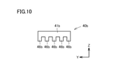
- FIG. 10 is a schematic plan view showing an enlarged part of a bus bar included in the semiconductor device according to the fourth embodiment.
- FIG. 11 is a schematic plan view showing an enlarged part of the semiconductor device according to the sixth embodiment.
- one of the purposes of the present disclosure is to provide a semiconductor device capable of improving the yield and reliability.
- the semiconductor device includes a drain terminal, a source terminal, and a gate terminal.
- the semiconductor device includes a first metal plate, a second metal plate arranged at intervals from the first metal plate, and a third metal arranged at intervals from each of the first metal plate and the second metal plate.
- the SiC transistor chip is provided with a second SiC transistor chip which is plate-shaped and is mounted on a first metal plate adjacent to the first SiC transistor chip.
- the first metal plate and the drain terminal are electrically connected.
- the second metal plate and the source terminal are electrically connected.
- the third metal plate and the gate terminal are electrically connected.
- the first SiC transistor chip includes a first source electrode pad and a first gate electrode pad arranged on one side in the thickness direction, and a first drain electrode pad arranged on the other side in the thickness direction.
- the second SiC transistor chip includes a second source electrode pad and a second gate electrode pad arranged on one side in the thickness direction, and a second drain electrode pad arranged on the other side in the thickness direction. , including.
- the first drain electrode pad is joined to the first metal plate.
- the second drain electrode pad is joined to the first metal plate.
- the semiconductor device includes a first conductor that electrically connects each of the first source electrode pad and the second source electrode pad and the second metal plate, and the first gate electrode pad and the second gate electrode pad.
- a second conductor that electrically connects each to the third metal plate, and one first wire that electrically connects the first source electrode pad, the second source electrode pad, and the fourth metal plate. To prepare for. At least one end of the first wire is joined to the fourth metal plate.
- the first SiC transistor chip and the second SiC transistor chip are mounted next to each other on the first metal plate.
- Such a first SiC transistor chip and a second SiC transistor chip are electrically connected in parallel.
- the SiC transistor chip refers to a transistor chip having a semiconductor layer made of SiC (silicon carbide) as an operating layer.
- the SiC transistor chip has low on-resistance and high withstand voltage. Therefore, the semiconductor device of the present disclosure adopting the above configuration in which a plurality of SiC transistor chips are connected in parallel can pass a large current.
- switching timing shifts may occur due to variations in the characteristics of each SiC transistor chip, and as a result, parasitic oscillation may occur. Since such parasitic oscillation may damage the transistor chip, it is required to suppress the parasitic oscillation.
- the first source electrode pad and the second source electrode pad are connected by the conductive first wire. Therefore, the potentials of the first source electrode pad and the second source electrode pad can be made the same. Therefore, parasitic oscillation can be suppressed.
- first source electrode pad and the second source electrode pad are electrically connected by the first wire, they may be connected by using wire bonding.
- wire connection using wire bonding each member and wire are connected one after another by ultrasonic bonding, and then the wire is finally cut.
- the blade of the cutter is pressed against the wire to cut the wire. If the SiC transistor chip comes into contact with the cutter blade when the wire is cut, the SiC transistor chip may be damaged. As a result, the yield at the time of manufacturing the semiconductor device is lowered.
- the semiconductor device of the present disclosure at least one end of the first wire is joined to the fourth metal plate. Therefore, the blade of the cutter can be pressed against the fourth metal plate to cut the wire. Therefore, it is possible to prevent the SiC transistor chip from coming into contact with the blade of the cutter when the wire is cut, and it is possible to reduce the risk of damage to the SiC transistor chip. Unlike the first metal plate connected to the drain terminal, a large current does not flow through the fourth metal plate. Therefore, even if the cutter blade is damaged, the reliability of the semiconductor device is not impaired. Therefore, it is possible to suppress a decrease in the yield of the semiconductor device at the time of manufacturing. From the above, according to the semiconductor device of the present disclosure, it is possible to improve the yield and the reliability.
- the above semiconductor device may further include a Kelvin terminal.
- the fourth metal plate and the Kelvin terminal may be electrically connected.
- a Kelvin terminal for controlling the gate voltage may be provided from the viewpoint of removing the influence of the parasitic inductance of the SiC transistor chips and reducing the switching loss.
- the Kelvin terminal forms a closed circuit with the gate terminal, and a large current does not flow. Therefore, in such a semiconductor device, the fourth metal plate can be effectively used as a configuration in which the fourth metal plate is connected to the Kelvin terminal, and the switching operation can be speeded up.
- the fourth metal plate may not be connected to each of the first metal plate, the second metal plate, and the third metal plate. By doing so, it is possible to obtain a fourth metal plate that is an electrically independent member, and even if the blade of the cutter comes into contact with the fourth metal plate and the fourth metal plate is damaged, the function as a semiconductor device is not impaired. Can be.
- the first wire may be arranged at a distance from each of the first conductor and the second conductor when viewed in the thickness direction of the first metal plate.
- the first conductor may be a bus bar (electrode plate).
- the parasitic inductance can be further reduced as compared with the case of connecting with a wire.
- soldering the bus bar it is possible to eliminate damage to the SiC transistor chip during wire bonding in connection using wires. Therefore, such a semiconductor device can further improve the yield and reliability.
- the first conductor may be a conductive second wire. By doing so, it is possible to electrically connect using the second wire in the same process as the first wire, and it is possible to improve the manufacturing efficiency.
- only one first wire may be used. By doing so, it is possible to improve the manufacturing efficiency.
- the semiconductor device of the present disclosure includes a drain terminal, a source terminal, a gate terminal, and a Kelvin terminal.
- the semiconductor device includes a first metal plate, a second metal plate arranged at intervals from the first metal plate, and a third metal arranged at intervals from each of the first metal plate and the second metal plate.
- the SiC transistor chip is provided with a second SiC transistor chip which is plate-shaped and is mounted on a first metal plate adjacent to the first SiC transistor chip. The first metal plate and the drain terminal are electrically connected.
- the second metal plate and the source terminal are electrically connected.
- the third metal plate and the gate terminal are electrically connected.
- the fourth metal plate and the Kelvin terminal are electrically connected.
- the fourth metal plate is not connected to each of the first metal plate, the second metal plate, and the third metal plate.
- the first SiC transistor chip includes a first source electrode pad and a first gate electrode pad arranged on one side in the thickness direction, and a first drain electrode pad arranged on the other side in the thickness direction. ,including.
- the second SiC transistor chip includes a second source electrode pad and a second gate electrode pad arranged on one side in the thickness direction, and a second drain electrode pad arranged on the other side in the thickness direction. ,including.
- the first drain electrode pad is joined to the first metal plate.
- the second drain electrode pad is joined to the first metal plate.
- the semiconductor device includes a first conductor that electrically connects each of the first source electrode pad and the second source electrode pad and the second metal plate, and the first gate electrode pad and the second gate electrode pad.
- a second conductor that electrically connects each to the third metal plate, and one first wire that electrically connects the first source electrode pad, the second source electrode pad, and the fourth metal plate.
- At least one end of the first wire is joined to the fourth metal plate.
- the first wire is arranged at a distance from each of the first conductor and the second conductor when viewed in the thickness direction of the first metal plate. There is only one first wire.
- FIG. 1 is a schematic plan view of the semiconductor device according to the first embodiment.
- FIG. 2 is a schematic plan view showing a part of the semiconductor device shown in FIG. 1 in an enlarged manner. In FIG. 2, the case described later shown in FIG. 1 is not shown.
- FIG. 3 is a schematic cross-sectional view showing a part of the semiconductor device shown in FIG. 1 in an enlarged manner.
- the semiconductor device 10a includes a drain terminal 31a, a source terminal 32a, a gate terminal 33a, and a Kelvin terminal 34a.
- the semiconductor device 10a includes a first metal plate 11a, a second metal plate 12a, a third metal plate 13a, a fourth metal plate 14a, and a first SiC transistor chip 21a arranged on the first metal plate 11a.
- a second SiC transistor chip 21b arranged on the first metal plate 11a, and a case 17a are included.
- the first metal plate 11a includes a substrate portion 15a having a rectangular shape when viewed in the thickness direction (Z direction) of the first metal plate 11a.
- the first metal plate 11a, the second metal plate 12a, the third metal plate 13a, and the fourth metal plate 14a constitute the lead frame 16a.
- the second metal plate 12a is arranged at a distance from the first metal plate 11a.
- the third metal plate 13a is arranged at a distance from each of the first metal plate 11a and the second metal plate 12a.
- the fourth metal plate 14a is arranged at intervals from each of the first metal plate 11a, the second metal plate 12a, and the third metal plate 13a.
- the semiconductor device 10a according to the first embodiment is a discrete device including a first SiC transistor chip 21a and a second SiC transistor chip 21b in a package.
- the first metal plate 11a, the second metal plate 12a, the third metal plate 13a, and the fourth metal plate 14a are each in the shape of a flat plate.
- a copper plate is adopted as the first metal plate 11a, the second metal plate 12a, the third metal plate 13a, and the fourth metal plate 14a.
- a thickness of this copper plate for example, one having a thickness of 1 mm is used.
- the first metal plate 11a and the drain terminal 31a are electrically connected to each other.
- the first metal plate 11a is integrally formed with the drain terminal 31a.
- the first metal plate 11a has a shape in which the drain terminal 31a is connected to the substrate portion 15a and is integrated.
- the second metal plate 12a and the source terminal 32a are electrically connected to each other.
- the second metal plate 12a is integrally formed with the source terminal 32a.
- the third metal plate 13a and the gate terminal 33a are electrically connected to each other.
- the third metal plate 13a is integrally formed with the gate terminal 33a.
- the fourth metal plate 14a and the Kelvin terminal 34a are electrically connected to each other.
- the fourth metal plate 14a is integrally formed with the Kelvin terminal 34a.
- the drain terminal 31a, the source terminal 32a, the gate terminal 33a, and the Kelvin terminal 34a each have a band-shaped shape.
- the drain terminal 31a, the source terminal 32a, the gate terminal 33a, and the Kelvin terminal 34a are arranged at intervals in the X direction, respectively.
- the drain terminal 31a, the source terminal 32a, the Kelvin terminal 34a, and the gate terminal 33a are arranged in this order in the direction of the arrow X.
- the semiconductor device 10a according to the first embodiment adopts a so-called four-terminal structure.
- An example of the boundary between the metal and the metal is shown by a broken line.
- the first SiC transistor chip 21a and the second SiC transistor chip 21b are so-called vertical semiconductor chips, for example, metal-oxide-semiconductor field effect transistors (MOSFETs).
- MOSFETs metal-oxide-semiconductor field effect transistors
- the first SiC transistor chip 21a and the second SiC transistor chip 21b are used as switching elements, respectively.
- the first SiC transistor chip 21a and the second SiC transistor chip 21b are connected in parallel.
- the first SiC transistor chip 21a and the second SiC transistor chip 21b each include a semiconductor layer made of silicon carbide (SiC) as an operating layer.
- SiC silicon carbide
- Such a first SiC transistor chip 21a and a second SiC transistor chip 21b have low on-resistance and high withstand voltage. Therefore, it is suitably used for semiconductor devices that carry a large current.
- the first SiC transistor chip 21a has a first drain electrode pad 22a located on one side in the thickness direction, a first source electrode pad 23a located on the other side in the thickness direction, and a first gate electrode pad. 24a and.
- the first drain electrode pad 22a of the first SiC transistor chip 21a is joined to the substrate portion 15a by, for example, solder (not shown). In this way, the first drain electrode pad 22a of the first SiC transistor chip 21a and the drain terminal 31a are electrically connected.
- the second SiC transistor chip 21b has a second drain electrode pad 22b located on one side in the thickness direction, a second source electrode pad 23b located on the other side in the thickness direction, and a second gate electrode pad. 24b and.
- the second drain electrode pad 22b of the second SiC transistor chip 21b is bonded to the substrate portion 15a by, for example, solder (not shown). In this way, the second drain electrode pad 22b of the second SiC transistor chip 21b and the drain terminal 31a are electrically connected.
- the first SiC transistor chip 21a and the second SiC transistor chip 21b are arranged on the substrate portion 15a at intervals in the Y direction, respectively. The positions of the first SiC transistor chip 21a and the second SiC transistor chip 21b in the X direction are the same.
- the case 17a is made of resin and is configured to cover the substrate portion 15a, the first SiC transistor chip 21a, the second SiC transistor chip 21b, and the wire described later.
- the case 17a has an insulating property. In this way, the substrate portion 15a, the first SiC transistor chip 21a, the second SiC transistor chip 21b, and the wire are sealed.
- the case 17a has a rectangular parallelepiped shape.
- the case 17a has a rectangular shape in which the length in the Y direction is longer than the length in the X direction when viewed in the thickness direction of the first metal plate 11a.
- the portions arranged in the case 17a constitute the first metal plate 11a, the second metal plate 12a, the third metal plate 13a, and the fourth metal plate 14, respectively.
- a portion exposed from one side of the rectangular case 17a constitutes a drain terminal 31a, a source terminal 32a, a gate terminal 33a, and a Kelvin terminal 34a, respectively. That is, in the present embodiment, the broken line indicates the boundary of the portion exposed from the case 17a.
- the case 17a is formed with a through hole 18a that penetrates in the thickness direction (Z direction).
- the first source electrode pad 23a of the first SiC transistor chip 21a is connected to the second metal plate 12a by two second wires 26a as the first conductor. Each of the two second wires 26a has conductivity. In this way, the first source electrode pad 23a of the first SiC transistor chip 21a is electrically connected to the source terminal 32a.
- the second source electrode pad 23b of the second SiC transistor chip 21b is connected to the second metal plate 12a by two second wires 26b as the first conductor. Each of the two second wires 26b has conductivity. In this way, the second source electrode pad 23b of the second SiC transistor chip 21b is electrically connected to the source terminal 32a.
- the first gate electrode pad 24a of the first SiC transistor chip 21a is connected to the third metal plate 13a by one third wire 27a as a second conductor.
- the third wire 27a has conductivity. In this way, the first gate electrode pad 24a of the first SiC transistor chip 21a is electrically connected to the gate terminal 33a.
- the second gate electrode pad 24b of the second SiC transistor chip 21b is connected to the third metal plate 13a by one third wire 27b as a second conductor.
- the third wire 27b has conductivity. In this way, the second gate electrode pad 24b of the second SiC transistor chip 21b is electrically connected to the gate terminal 33a.
- connection by the second wires 26a, 26b and the third wires 27a, 27b is carried out by using wire bonding, for example, using a wire bonder (not shown) equipped with a bond tool (not shown) from the viewpoint of manufacturing efficiency. be able to.
- the semiconductor device 10a includes one conductive first wire 28a.
- the first wire 28a electrically connects the first source electrode pad 23a, the second source electrode pad 23b, and the fourth metal plate 14a.
- One end 29a of the first wire 28a is joined to the first source electrode pad 23a.
- the other end 29c of the first wire 28a is joined to the fourth metal plate 14a.
- the first wire 28a is arranged at intervals from the second wires 26a and 26b, which are the first conductors, and the third wires 27a, 27b, which are the second conductors, when viewed in the thickness direction of the first metal plate 11a. Has been done. That is, the first wire 28a does not intersect the second wires 26a and 26b and the third wires 27a and 27b, respectively, when viewed in the thickness direction of the first metal plate 11a.
- the manufacturing method of the semiconductor device 10a will be briefly described.
- the first SiC transistor chip 21a and the second SiC transistor chip 21b are soldered to the substrate portion 15a. Join on top. Then, using wire bonding, each member is electrically connected by a wire.
- the joining of the first wire 28a is performed as follows. First, one end 29a of the wire, in this case, the tip of the wire is placed on the first source electrode pad 23a, and the tip of the wire bonder is pressed from above the wire. In such a state, one end 29a of the wire is ultrasonically bonded to the first source electrode pad 23a. Next, the wire bonder is moved onto the second source electrode pad 23b of the second SiC transistor chip 21b while supplying the wire. Then, at the bonding portion 29b, the wire and the first source electrode pad 23a are ultrasonically bonded by a wire bonder. Next, the wire supply unit is moved onto the fourth metal plate 14a while supplying the wire.
- the wire and the fourth metal plate 14a are ultrasonically bonded by a wire bonder.
- the cutter is pressed against the wire of the ultrasonically bonded portion to cut the wire.
- the other end 29c of the wire will be joined to the fourth metal plate 14a. In this way, the first wire 28a is joined.
- the other end 29c of the first wire 28a is joined to the fourth metal plate 14a. Therefore, the blade of the cutter can be pressed onto the fourth metal plate 14a to cut the wire. Therefore, when the wire is cut, the contact between the first SiC transistor chip 21a and the second SiC transistor chip 21b and the blade of the cutter can be prevented, and the first SiC transistor chip 21a and the second SiC transistor can be prevented. The risk of damage to the chip 21b can be reduced. Therefore, it is possible to suppress a decrease in the yield of the semiconductor device 10a at the time of manufacturing. As a result, such a semiconductor device 10a can improve the yield and the reliability.
- the fourth metal plate 14a and the Kelvin terminal 34a are electrically connected. Therefore, it is possible to reduce the switching loss by removing the influence of the parasitic inductance of the first SiC transistor chip 21a and the second SiC transistor chip 21b. Further, the Kelvin terminal 34a forms a closed circuit with the gate terminal 33a, and a large current does not flow. Therefore, such a semiconductor device 10a is a semiconductor device capable of effectively utilizing the fourth metal plate 14a as a configuration in which the fourth metal plate 14a is connected to the Kelvin terminal 34a and speeding up the switching operation. There is.
- the first wire 28a is a first conductor, the second wire 26a, 26b, and the second conductor, the third wire 27a, 27b, respectively, when viewed in the thickness direction of the first metal plate 11a. And are arranged at intervals. Therefore, it is possible to reduce the possibility that the first wire 28a and the second wires 26a and 26b and the third wires 27a and 27b each interfere with each other. Therefore, the semiconductor device 10a is a semiconductor device that facilitates wire bonding and can improve manufacturing efficiency.
- the first conductor is the conductive second wires 26a and 26b. Therefore, the second wires 26a and 26b can be used for electrical connection in the same process as the first wire 28a. Therefore, the semiconductor device 10a is a semiconductor device capable of improving manufacturing efficiency. In this embodiment, the third wires 27a and 27b can be used for connection in the same process as the first wire 28a.
- the semiconductor device 10a includes a drain terminal 31a, a source terminal 32a, a gate terminal 33a, and a Kelvin terminal 34a.
- the semiconductor device 10a is spaced from the first metal plate 11a, the second metal plate 12a arranged at intervals from the first metal plate 11a, and the first metal plate 11a and the second metal plate 12a, respectively.
- a transistor chip 21b is provided.
- the first metal plate 11a and the drain terminal 31a are electrically connected to each other.
- the second metal plate 12a and the source terminal 32a are electrically connected to each other.
- the third metal plate 13a and the gate terminal 33a are electrically connected to each other.
- the fourth metal plate 14a and the Kelvin terminal 34a are electrically connected to each other.
- the fourth metal plate 14a is not connected to each of the first metal plate 11a, the second metal plate 12a, and the third metal plate 13a.
- the first SiC transistor chip 21a has a first source electrode pad 23a and a first gate electrode pad 24a arranged on one side in the thickness direction, and a first drain arranged on the other side in the thickness direction.
- the electrode pad 22a and the like are included.
- the second SiC transistor chip 21b has a second source electrode pad 23b and a second gate electrode pad 24b arranged on one side in the thickness direction, and a second drain arranged on the other side in the thickness direction. Includes electrode pads 22b and.
- the first drain electrode pad 22a is joined to the first metal plate 11a.
- the second drain electrode pad 22b is joined to the first metal plate 11a.
- the second wires 26a and 26b as the first conductor for electrically connecting each of the first source electrode pad 23a and the second source electrode pad 23b and the second metal plate 12a, and the first one.
- the third wires 27a and 27b as the second conductor for electrically connecting each of the gate electrode pads 24a and the second gate electrode pads 24b and the third metal plate 13a, and the first source electrode pads 23a and the first.
- a first wire 28a for electrically connecting the source electrode pad 23b of 2 and the fourth metal plate 14a is provided.
- the other end 29c of the first wire 28a is joined to the fourth metal plate 14a.
- the first wire 28a is arranged at intervals from the second wires 26a and 26b, which are the first conductors, and the third wires 27a, 27b, which are the second conductors, when viewed in the thickness direction of the first metal plate 11a. Has been done. There is only one first wire 28a.
- FIG. 4 is a schematic plan view showing an enlarged part of the semiconductor device according to the second embodiment.
- the semiconductor device of the second embodiment is different from the case of the first embodiment in that the second wires, which are the first conductors, intersect with each other when viewed in the thickness direction of the first metal plate 11a.
- the positions of the first SiC transistor chip 21a and the second SiC transistor chip 21b included in the semiconductor device 10b of the second embodiment are different in the X direction.
- the second SiC transistor chip 21b is arranged so as to be closer to the drain terminal 31a than the first SiC transistor chip 21a.
- the second wire 26a as the first conductor intersects the second wire 26b when viewed in the thickness direction of the first metal plate 11a.
- the semiconductor device 10b is a semiconductor device capable of improving reliability. In the present embodiment, it is possible to increase the degree of freedom in the arrangement and orientation of the first SiC transistor chip 21a and the second SiC transistor chip 21b on the substrate portion 15a.
- FIG. 5 is a schematic plan view showing an enlarged part of the semiconductor device according to the third embodiment.
- the semiconductor device of the third embodiment is different from the case of the first embodiment and the second embodiment in that the Kelvin terminal is not included and the first wire intersects the second conductor.
- the positions of the first SiC transistor chip 21a and the second SiC transistor chip 21b included in the semiconductor device 10c of the third embodiment are different in the X direction.
- the first SiC transistor chip 21a is arranged so as to be closer to the drain terminal 31a than the second SiC transistor chip 21b.
- the first wire 28a intersects with the third wire 27a as the second conductor when viewed in the thickness direction of the first metal plate 11a.
- the fourth metal plate 14a included in the semiconductor device 10c of the third embodiment is not exposed from the case 17a.
- the semiconductor device 10c of the third embodiment does not include the Kelvin terminal 34a included in the semiconductor devices 10a and 10b of the first embodiment and the second embodiment.
- the semiconductor device 10c according to the third embodiment adopts a three-terminal structure.
- the fourth metal plate 14a is not connected to any of the first metal plate 11a, the second metal plate 12a, and the third metal plate 13a.
- the fourth metal plate 14a is used for cutting the first wire 28a during manufacturing.
- the semiconductor device 10c of the present embodiment is a semiconductor device capable of improving reliability.
- the semiconductor device 10c of the present embodiment is preferably used when adopting a three-terminal structure without a Kelvin terminal.
- the semiconductor device may be configured to incorporate a diode chip that suppresses the flow of current in the reverse direction in the electric circuit. By doing so, the risk of damage to the first SiC transistor chip 21a and the second SiC transistor chip 21b can be reduced, and the reliability of the semiconductor device can be further improved.
- FIG. 6 is a schematic plan view showing an enlarged part of the semiconductor device according to the fourth embodiment.
- FIG. 7 is a schematic side view when a part of the semiconductor device shown in FIG. 6 is viewed in the direction indicated by the arrow X.
- FIG. 8 is a schematic side view of a part of the semiconductor device shown in FIG. 6 when viewed in the Y direction.
- FIG. 9 is a schematic side view when a part of the semiconductor device shown in FIG. 6 is viewed in the direction opposite to the direction indicated by the arrow X.
- the semiconductor device of the fourth embodiment is different from the case of the first embodiment in that a bus bar (electrode plate) is used instead of the wire as the first conductor and that the semiconductor device has a diode chip.
- a bus bar electrode plate
- the semiconductor device 10d of the fourth embodiment includes a first metal plate 11a, a second metal plate 12a, a third metal plate 13a, and a fourth metal.
- the case 17d is formed so as to surround the substrate portion 15a.
- the diode chip 36a is a so-called vertical semiconductor chip, for example, a Schottky barrier diode (SBD).
- SBD Schottky barrier diode
- a SiC diode chip including a semiconductor layer made of silicon carbide (SiC) as an operating layer is adopted from the viewpoint of low on-resistance and high withstand voltage.
- the diode chip 36a is arranged on the first metal plate 11a. In the present embodiment, the diode chip 36a is arranged on the substrate portion 15a of the first metal plate 11a.
- the diode chip 36a has a plate shape.
- the diode chip 36a includes a cathode electrode pad 37a located on one side in the thickness direction and an anode electrode pad 38a located on the other side in the thickness direction.
- the diode chip 36a is arranged on the substrate portion 15a by joining the cathode electrode pad 37a to the substrate portion 15a, for example, by soldering (not shown). By adopting a configuration including such a diode chip 36a, it is possible to suppress the flow of current in the reverse direction.
- the bus bar 40a has, for example, a bent steel strip.
- the bus bar 40a is connected to a band-shaped first portion 41a extending in the Y direction and a first portion 41a, and is connected to a second portion 42a bent in a semicircular shape in the thickness direction and a second portion 42a, and is in a flat plate shape. It includes a third portion 43a, a fourth portion 44a extending in an inclined manner connected to the third portion 43a, and a flat plate-shaped fifth portion 45a connected to the fourth portion 44a and parallel to the third portion 43a.
- the first portion 41a is arranged so as to straddle the first SiC transistor chip 21a and the second SiC transistor chip 21b.
- the third portion 43a is arranged on the diode chip 36a.
- the fifth portion 45a is arranged on the second metal plate 12a constituting the lead frame 16a.
- the first portion 41a, the first SiC transistor chip 21a, and the second SiC transistor chip 21b are each joined by solder (not shown).
- the third portion 43a and the diode chip 36a are joined by solder (not shown).
- the fifth portion 45a and the second metal plate 12a are joined by solder (not shown).
- the first conductor connecting each of the first source electrode pad 23a and the second source electrode pad 23b to the second metal plate 12a is a bus bar 40a.
- the parasitic inductance can be further reduced as compared with the case of connecting with a wire.
- soldering the bus bar 40a it is possible to eliminate damage to the first SiC transistor chip 21a and the second SiC transistor chip 21b during wire bonding in the connection using wires. Therefore, such a semiconductor device 10d is a semiconductor device capable of further improving the yield and reliability.
- FIG. 10 is a schematic plan view showing an enlarged part of a bus bar included in the semiconductor device according to the fourth embodiment.
- the semiconductor device of the fifth embodiment is different from the case of the fourth embodiment in the shape of the first portion of the bus bar.
- the first portion 41b of the bus bar 40b included in the semiconductor device of the fifth embodiment includes a plurality of protrusions 46b.
- the protrusions 46b are formed so as to extend in the Z direction with a gap in the Y direction.
- the tip of the protrusion 46b in the Z direction is formed of a flat surface.
- it is joined to each of the first SiC transistor chip 21a and the second SiC transistor chip 21b.
- FIG. 11 is a schematic plan view showing an enlarged part of the semiconductor device according to the sixth embodiment.
- the semiconductor device 10e of the sixth embodiment includes a first metal plate 11a, a second metal plate 12a, a third metal plate 13a, a fourth metal plate 14a, and a first metal plate 11a.
- the first conductor connecting each of the first source electrode pad 23a and the second source electrode pad 23b to the second metal plate 12a is a bus bar 40a.
- the parasitic inductance can be further reduced. Therefore, such a semiconductor device 10e is a semiconductor device capable of further improving the yield and reliability.
- the SiC transistor chip is included, but the present invention is not limited to this, and the operating layer may include another semiconductor layer, for example, a semiconductor layer composed of gallium nitride or gallium oxide. good.
- SiC transistor chips connected in parallel are included, but the present invention is not limited to this, and three or more SiC transistor chips connected in parallel may be included.
- the number of the first wire is only one, but the present invention is not limited to this, and two or more first wires, that is, a plurality of the first wires may be included.
- the present invention is not limited to this, and one end of the first wire is the fourth metal plate. It may be joined to. Further, both ends of the first wire may be joined to the fourth metal plate. In this case, a plurality of fourth metal plates may be provided.
- the first metal plate 11a and the drain terminal 31a are integrally configured, but the present invention is not limited to this, and the first metal plate 11a and the drain terminal 31a are each configured. It is composed of a separate member, and the first metal plate 11a and the drain terminal 31a may be electrically connected by a member having conductivity.
- the second metal plate 12a and the source terminal 32a may be electrically connected by a conductive member.
- the third metal plate 13a and the gate terminal 33a are integrally configured, but the present invention is not limited to this, and the third metal plate 13a and the gate terminal 33a are each composed of separate members, and the third metal plate 13a and the gate terminal 33a are configured as separate members.
- the metal plate 13a and the gate terminal 33a may be electrically connected by a conductive member.
- the fourth metal plate 14a and the Kelvin terminal 34a are integrally configured, but the present invention is not limited to this, and the fourth metal plate 14a and the Kelvin terminal 34a are each composed of separate members, and the fourth metal plate 14a and the Kelvin terminal 34a are configured as separate members.
- the metal plate 14a and the Kelvin terminal 34a may be electrically connected by a conductive member.
- 10a, 10b, 10c, 10d, 10e Semiconductor device, 11a 1st metal plate, 12a 2nd metal plate, 13a 3rd metal plate, 14a 4th metal plate, 15a substrate part, 16a lead frame, 17a, 17d case, 18a Through hole, 21a first SiC transistor chip, 21b second SiC transistor chip, 22a first drain electrode pad, 22b second drain electrode pad, 23a first source electrode pad, 23b second source electrode pad , 24a 1st gate electrode pad, 24b 2nd gate electrode pad, 26a, 26b 2nd wire, 27a, 27b 3rd wire, 28a 1st wire, 29a, 29c end, 29b joint, 31a drain terminal, 32a source terminal, 33a gate terminal, 34a Kelvin terminal, 36a diode chip, 37a cathode electrode pad, 38a anode electrode pad, 40a, 40b bus bar, 41a, 41b 1st part, 42a 2nd part, 43a 3rd part, 44a 1st 4 parts
Landscapes
- Junction Field-Effect Transistors (AREA)
- Electrodes Of Semiconductors (AREA)
Priority Applications (1)
| Application Number | Priority Date | Filing Date | Title |
|---|---|---|---|
| JP2022546188A JPWO2022049999A1 (https=) | 2020-09-01 | 2021-08-06 |
Applications Claiming Priority (2)
| Application Number | Priority Date | Filing Date | Title |
|---|---|---|---|
| JP2020146874 | 2020-09-01 | ||
| JP2020-146874 | 2020-09-01 |
Publications (1)
| Publication Number | Publication Date |
|---|---|
| WO2022049999A1 true WO2022049999A1 (ja) | 2022-03-10 |
Family
ID=80491992
Family Applications (1)
| Application Number | Title | Priority Date | Filing Date |
|---|---|---|---|
| PCT/JP2021/029378 Ceased WO2022049999A1 (ja) | 2020-09-01 | 2021-08-06 | 半導体装置 |
Country Status (2)
| Country | Link |
|---|---|
| JP (1) | JPWO2022049999A1 (https=) |
| WO (1) | WO2022049999A1 (https=) |
Citations (2)
| Publication number | Priority date | Publication date | Assignee | Title |
|---|---|---|---|---|
| WO2018198957A1 (ja) * | 2017-04-24 | 2018-11-01 | ローム株式会社 | 半導体装置 |
| WO2020059285A1 (ja) * | 2018-09-20 | 2020-03-26 | 富士電機株式会社 | 半導体装置 |
-
2021
- 2021-08-06 JP JP2022546188A patent/JPWO2022049999A1/ja not_active Withdrawn
- 2021-08-06 WO PCT/JP2021/029378 patent/WO2022049999A1/ja not_active Ceased
Patent Citations (2)
| Publication number | Priority date | Publication date | Assignee | Title |
|---|---|---|---|---|
| WO2018198957A1 (ja) * | 2017-04-24 | 2018-11-01 | ローム株式会社 | 半導体装置 |
| WO2020059285A1 (ja) * | 2018-09-20 | 2020-03-26 | 富士電機株式会社 | 半導体装置 |
Also Published As
| Publication number | Publication date |
|---|---|
| JPWO2022049999A1 (https=) | 2022-03-10 |
Similar Documents
| Publication | Publication Date | Title |
|---|---|---|
| US8461623B2 (en) | Power semiconductor module | |
| JP5232367B2 (ja) | 半導体装置 | |
| TWI614877B (zh) | 半導體裝置 | |
| JP4865829B2 (ja) | 半導体装置およびその製造方法 | |
| JP5714916B2 (ja) | 半導体装置およびその製造方法 | |
| JP2009231805A (ja) | 半導体装置 | |
| KR20080096483A (ko) | 반도체 장치 | |
| CN104821282A (zh) | 功率半导体组件 | |
| JPWO2015111691A1 (ja) | 電極端子、電力用半導体装置、および電力用半導体装置の製造方法 | |
| US9159715B2 (en) | Miniaturized semiconductor device | |
| US11996344B2 (en) | Semiconductor device | |
| US20230395451A1 (en) | Semiconductor device and manufacturing method for semiconductor device | |
| JP7545845B2 (ja) | 半導体装置 | |
| CN109564918B (zh) | 半导体装置 | |
| US20250301761A1 (en) | Semiconductor device | |
| JP2022074290A (ja) | 半導体装置 | |
| JP7835681B2 (ja) | 半導体装置 | |
| WO2022049999A1 (ja) | 半導体装置 | |
| CN113363228A (zh) | 半导体装置 | |
| US20230136604A1 (en) | Semiconductor device | |
| CN115116977A (zh) | 半导体装置及其制造方法 | |
| KR20220063570A (ko) | 반도체 소자 패키지 | |
| CN223566612U (zh) | 一种GaN芯片的封装结构和电子设备 | |
| WO2020166283A1 (ja) | 半導体装置 | |
| US12327780B2 (en) | Semiconductor device including a lead and a sealing resin |
Legal Events
| Date | Code | Title | Description |
|---|---|---|---|
| 121 | Ep: the epo has been informed by wipo that ep was designated in this application |
Ref document number: 21864057 Country of ref document: EP Kind code of ref document: A1 |
|
| ENP | Entry into the national phase |
Ref document number: 2022546188 Country of ref document: JP Kind code of ref document: A |
|
| NENP | Non-entry into the national phase |
Ref country code: DE |
|
| 122 | Ep: pct application non-entry in european phase |
Ref document number: 21864057 Country of ref document: EP Kind code of ref document: A1 |