WO2022049770A1 - 光デバイス - Google Patents
光デバイス Download PDFInfo
- Publication number
- WO2022049770A1 WO2022049770A1 PCT/JP2020/033787 JP2020033787W WO2022049770A1 WO 2022049770 A1 WO2022049770 A1 WO 2022049770A1 JP 2020033787 W JP2020033787 W JP 2020033787W WO 2022049770 A1 WO2022049770 A1 WO 2022049770A1
- Authority
- WO
- WIPO (PCT)
- Prior art keywords
- core
- metal layer
- layer
- optical device
- optical waveguide
- Prior art date
- Legal status (The legal status is an assumption and is not a legal conclusion. Google has not performed a legal analysis and makes no representation as to the accuracy of the status listed.)
- Ceased
Links
Images


Classifications
-
- G—PHYSICS
- G02—OPTICS
- G02F—OPTICAL DEVICES OR ARRANGEMENTS FOR THE CONTROL OF LIGHT BY MODIFICATION OF THE OPTICAL PROPERTIES OF THE MEDIA OF THE ELEMENTS INVOLVED THEREIN; NON-LINEAR OPTICS; FREQUENCY-CHANGING OF LIGHT; OPTICAL LOGIC ELEMENTS; OPTICAL ANALOGUE/DIGITAL CONVERTERS
- G02F1/00—Devices or arrangements for the control of the intensity, colour, phase, polarisation or direction of light arriving from an independent light source, e.g. switching, gating or modulating; Non-linear optics
- G02F1/01—Devices or arrangements for the control of the intensity, colour, phase, polarisation or direction of light arriving from an independent light source, e.g. switching, gating or modulating; Non-linear optics for the control of the intensity, phase, polarisation or colour
- G02F1/03—Devices or arrangements for the control of the intensity, colour, phase, polarisation or direction of light arriving from an independent light source, e.g. switching, gating or modulating; Non-linear optics for the control of the intensity, phase, polarisation or colour based on ceramics or electro-optical crystals, e.g. exhibiting Pockels effect or Kerr effect
- G02F1/035—Devices or arrangements for the control of the intensity, colour, phase, polarisation or direction of light arriving from an independent light source, e.g. switching, gating or modulating; Non-linear optics for the control of the intensity, phase, polarisation or colour based on ceramics or electro-optical crystals, e.g. exhibiting Pockels effect or Kerr effect in an optical waveguide structure
Definitions
- the present invention relates to an optical device using an electro-optical material.
- the optical waveguide type high-speed phase shifter is being researched and developed as a key device with the aim of applying it to various applications using Tbit / s class ultra-high-speed optical communication and millimeter waves and terahertz waves.
- high-speed phase shifters there is a plasmonic optical waveguide type phase shifter in which an electro-optic (EO) material is used for an optical waveguide core.
- EO electro-optic
- the plasmonic optical waveguide type phase shifter is capable of high-speed operation because it uses a dielectric response by an externally modulated electric field as its operating principle to cause a change in refractive index and can realize an ultra-compact phase shifter. It has the feature.
- Non-Patent Document 1 a phase shifter using BaTiO 3 (BTO) as an EO material has been proposed (see Non-Patent Document 1).
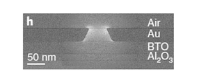
- a core made of BTO is sandwiched by a metal layer made of gold (Au) to form a plasmonic optical waveguide (see FIG. 6).
- Au gold
- the angle of the core side wall is 70 to 80 ° in cross-sectional view, not perpendicular to the plane of the substrate (90 °).
- phase shifter using the plasmonic optical waveguide with the EO material as the core has the following problems.
- the angle of the core side wall deviates from 90 ° with respect to the plane of the substrate.
- the photoelectric propagating through the plasmonic optical waveguide propagates.
- the magnetic field distribution is more concentrated at the boundary between the metal layer and the core near the top of the cross-sectional spectroscopic core.
- the modulated electric field that drives the phase shifter is more evenly distributed between the left and right metal layers of the core. For this reason, in the conventional technique, the overlap between the photoelectric magnetic field and the modulated electric field is reduced, which leads to a reduction in the amount of change in the refractive index for shifting the propagating light phase.
- modulation efficiency has been sacrificed.
- the plasmonic optical waveguide since the plasmonic optical waveguide has a higher light intensity per unit cross-sectional area than a normal dielectric optical waveguide, it leads to more localization of the power of the input light, and the light intensity per unit cross-sectional area increases. There was a problem that it became larger and the possibility of light loss increased.
- the present invention has been made to solve the above problems, and is to improve modulation efficiency and reduce optical loss in an optical device composed of a plasmonic optical waveguide using a core composed of an electro-optical material.
- the purpose is suppression.
- the optical device according to the present invention is formed on both sides of a slab layer made of a material having an electro-optical effect, a core made of the same material as the slab layer formed on the slab layer, and a core made of the same material as the slab layer.
- the plasmonic optical waveguide is composed of the core, the first metal layer, and the second metal layer, and both sides of the core are with the bottom surface on the side of the slab layer.
- the angle formed is said to be an acute angle of 85 ° or more.
- the angle between both sides and the bottom surface on the side of the slab layer of a core made of a material having an electro-optic effect constituting a plasmonic optical waveguide is 85 °. Since the above sharp angle is obtained, it is possible to improve the modulation efficiency and suppress the optical loss in the optical device composed of the plasmonic optical waveguide using the core composed of the electro-optical material.
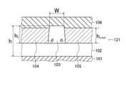
- FIG. 1 is a cross-sectional view showing the configuration of an optical device according to an embodiment of the present invention.
- FIG. 2 is a characteristic diagram showing the relationship between the angle ⁇ formed with the bottom surface on the side of the slab layer 102 and the change in modulation efficiency.
- FIG. 4 is a cross-sectional view showing the configuration of the optical waveguide region 123.
- FIG. 5 is a perspective view showing a configuration of an optical device according to an embodiment of the present invention.
- FIG. 6 shows Fig. 6 of Non-Patent Document 1. It is a block diagram which shows the cross section of the phase shifter (plasmonic optical waveguide) shown by h of 2.
- FIG. 1 shows a cross section of a surface perpendicular to the waveguide direction.
- the optical device comprises a phase shifter 121, which comprises a slab layer 102 and a core 103 formed on the slab layer 102.
- a well-known rib-type optical waveguide is configured in the core 103 and the slab layer 102.
- this optical device includes a first metal layer 104 and a second metal layer 105 formed on both side surfaces of the core 103.
- the plasmonic optical waveguide is composed of the core 103, the first metal layer 104, and the second metal layer 105.
- the lower clad layer 101 is formed under the slab layer 102, and the first metal layer 104, the second metal layer 105, and the upper clad layer 106 formed on the upper part of the core 103 are provided.
- the lower clad layer 101 and the upper clad layer 106 may be omitted.
- the slab layer 102 is made of a material having an electro-optical effect.
- the core 103 is made of a material having the same electro-optic effect as the slab layer 102.
- the slab layer 102 and the core 103 can be integrally formed.
- This material can be composed of, for example, lithium niobate (LiNbO 3 ).
- the above-mentioned materials include, for example, strong dielectric perovskite oxide crystals such as BaTiO 3 , LiNbO 3 , LiTaO 3 , and KTN, and cubic perovskite oxidation such as KTN, BaTiO 3 , SrTiO 3 , and Pb 3 MgNb 2 O 9 . It can also be a physical crystal. Further, the above-mentioned material may be KDP type crystal, sphalerite type crystal or the like.
- both side surfaces of the core 103 have an acute angle of 85 ° or more with the bottom surface on the side of the slab layer 102.
- the cross-sectional shape of the core 103 is an isosceles trapezoid.
- the core 103 is a prism that is a trajectory of an isosceles trapezoid translated in the waveguide direction, and has two parallel first and second surfaces and two adjacent third and fourth surfaces.
- the first surface which is provided with a surface and has a long length in the direction perpendicular to the waveguide direction, is arranged as the side of the slab layer 102.
- the angle ⁇ formed by the first surface and the third surface and the angle ⁇ formed by the first surface and the fourth surface are set to be an acute angle of 85 ° or more.
- the first metal layer 104 and the second metal layer 105 are formed in contact with both side surfaces (third surface and fourth surface) of the core 103.
- the first metal layer 104 and the second metal layer 105 are made of, for example, Au.
- the first metal layer 104 and the second metal layer 105 may be any metal as long as they can excite surface plasmon polaritons (SPP) at the interface with the core 103 with respect to light having a wavelength waveguideed through the plasmonic optical waveguide.
- SPP surface plasmon polaritons
- Au for example, Ag, Al, Cu, Ti, Pt and the like can be applied.
- the lower clad layer 101 and the upper clad layer 106 can be made of an oxide such as silicon oxide. They can also be layers of air.
- the angle ⁇ between both side surfaces and the bottom surface of the core 103 in cross-sectional view is set to a value close to 90 degrees
- the light flowing through the plasmonic optical waveguide is set to a value close to 90 degrees.
- An excellent effect is obtained that the optical magnetic field intensity distribution is suppressed from being concentrated at the boundary between the first metal layer 104, the second metal layer 105, and the core 103 near the top of the core 103.
- the overlap between the photoelectric magnetic field of the light guided through the plasmonic optical waveguide and the modulation electric field is increased, and an excellent effect of increasing the modulation efficiency can be obtained.
- the modulation efficiency becomes 1.5 times or more.
- ⁇ 90 ° or more and a larger value (obtuse angle)
- the distance between the first metal layer 104 and the second metal layer 105 is smaller, such as when ⁇ of 90 ° or less is small. It can be easily inferred that the photoelectric magnetic field intensity distribution is concentrated and the modulation efficiency is reduced.
- the angle ⁇ between the side surface and the bottom surface of the core 103 in a cross-sectional view to be an acute angle of 85 ° or more, an excellent effect that the modulation efficiency can be further increased can be obtained.
- a photoelectric magnetic field is formed at the boundary between the first metal layer 104 and the second metal layer 105 and the core 103 near the top of the core 103 having a trapezoidal cross-sectional shape. Is suppressed, and an excellent effect that the photoelectric magnetic field can be widely distributed in the core 103 can be obtained. This leads to suppression of the possibility of light damage (light loss) of the core 103 at the boundary between the first metal layer 104 and the second metal layer 105 and the core 103 near the top of the core 103.
- FIG. 3 shows the relationship between ⁇ obtained by calculation and the modulation efficiency.
- the modulation efficiency is set to the absolute value [abs (dn / dV)] of the amount of change in the effective refractive index of the propagation mode per unit modulation voltage.
- FIG. 3 shows a case where the first metal layer 104 and the second metal layer 105 are used as electrodes, respectively, and a case where 5V is applied as a DC bias between them and a case where 10V is applied. It can be seen that in each case, the modulation efficiency increases as ⁇ approaches 90 °. In this way, high modulation efficiency can be obtained by bringing ⁇ close to 90 °.
- This type of optical waveguide structure generally uses a so-called low-loss manufacturing process, such as lowering the process temperature, in order to suppress the occurrence of damage to each part.
- a so-called low-loss manufacturing process such as lowering the process temperature
- the value of is determined by lithography at the time of pattern formation of the core 103. Therefore, if the value of h metal is close to the value of h 2 , the distance between the first metal layer 104 and the second metal layer 105 will be narrower, that is, the modulated electric field will be increased. This makes it possible to increase the modulation efficiency.
- the optical device is used by optically connecting the phase shifter 121 to the optical waveguide region 123 as shown in FIG.
- the phase shifter 121 and the optical waveguide region 123 are monolithically integrated on the same lower clad layer 101, as shown in FIG.
- the core 103 of the phase shifter 121 is provided with a mode conversion region 122 on one end side in which the width (core width) in a plan view gradually expands in the waveguide direction, and the phase shifter 121 and the optical waveguide region are provided via the mode conversion region 122.
- 123 is optically connected.
- the mode conversion region 122 is continuously formed in the phase shifter 121, and the optical waveguide region 123 is formed following the mode conversion region 122.
- the optical waveguide region 123 is composed of a core 103a and an upper clad layer (not shown) covering the core 103a, and the first metal layer 104 and the second metal layer 105 are not formed. Further, in the optical waveguide region 123, the core width W 2 of the core 103a is, for example, 800 nm, which is wider than the core width W of the phase shifter 121.
- the optical waveguide region 123 and the plasmonic optical waveguide constituting the phase shifter 121 can be integrated on the same substrate.
- the angle between both sides and the bottom surface on the side of the slab layer of a core made of a material having an electro-optic effect constituting a plasmonic optical waveguide is 85. Since the angle is sharper than °, it is possible to improve the modulation efficiency and suppress the optical loss in the optical device composed of the plasmonic optical waveguide using the core composed of the electro-optical material.
Landscapes
- Physics & Mathematics (AREA)
- Nonlinear Science (AREA)
- Chemical & Material Sciences (AREA)
- Engineering & Computer Science (AREA)
- Ceramic Engineering (AREA)
- Crystallography & Structural Chemistry (AREA)
- General Physics & Mathematics (AREA)
- Optics & Photonics (AREA)
- Optical Modulation, Optical Deflection, Nonlinear Optics, Optical Demodulation, Optical Logic Elements (AREA)
Priority Applications (2)
| Application Number | Priority Date | Filing Date | Title |
|---|---|---|---|
| JP2022546856A JPWO2022049770A1 (https=) | 2020-09-07 | 2020-09-07 | |
| PCT/JP2020/033787 WO2022049770A1 (ja) | 2020-09-07 | 2020-09-07 | 光デバイス |
Applications Claiming Priority (1)
| Application Number | Priority Date | Filing Date | Title |
|---|---|---|---|
| PCT/JP2020/033787 WO2022049770A1 (ja) | 2020-09-07 | 2020-09-07 | 光デバイス |
Publications (1)
| Publication Number | Publication Date |
|---|---|
| WO2022049770A1 true WO2022049770A1 (ja) | 2022-03-10 |
Family
ID=80490860
Family Applications (1)
| Application Number | Title | Priority Date | Filing Date |
|---|---|---|---|
| PCT/JP2020/033787 Ceased WO2022049770A1 (ja) | 2020-09-07 | 2020-09-07 | 光デバイス |
Country Status (2)
| Country | Link |
|---|---|
| JP (1) | JPWO2022049770A1 (https=) |
| WO (1) | WO2022049770A1 (https=) |
Citations (3)
| Publication number | Priority date | Publication date | Assignee | Title |
|---|---|---|---|---|
| WO2008102511A1 (ja) * | 2007-02-19 | 2008-08-28 | Nec Corporation | 光位相変調素子およびこれを用いた光変調器 |
| US20130050788A1 (en) * | 2011-08-24 | 2013-02-28 | Samsung Electronics Co., Ltd. | Acousto-optic device having nanostructure, and optical scanner, optical modulator, and display apparatus using the acousto-optic device |
| JP2018004932A (ja) * | 2016-07-01 | 2018-01-11 | 日本電信電話株式会社 | 光位相・強度シフタ |
Family Cites Families (3)
| Publication number | Priority date | Publication date | Assignee | Title |
|---|---|---|---|---|
| JP2009258527A (ja) * | 2008-04-21 | 2009-11-05 | Hitachi Ltd | 光学素子 |
| JP6409299B2 (ja) * | 2014-03-27 | 2018-10-24 | 日本電気株式会社 | 光変調用素子および光変調器 |
| WO2016154764A2 (en) * | 2015-04-01 | 2016-10-06 | ETH Zürich | Electrooptic modulator |
-
2020
- 2020-09-07 WO PCT/JP2020/033787 patent/WO2022049770A1/ja not_active Ceased
- 2020-09-07 JP JP2022546856A patent/JPWO2022049770A1/ja active Pending
Patent Citations (3)
| Publication number | Priority date | Publication date | Assignee | Title |
|---|---|---|---|---|
| WO2008102511A1 (ja) * | 2007-02-19 | 2008-08-28 | Nec Corporation | 光位相変調素子およびこれを用いた光変調器 |
| US20130050788A1 (en) * | 2011-08-24 | 2013-02-28 | Samsung Electronics Co., Ltd. | Acousto-optic device having nanostructure, and optical scanner, optical modulator, and display apparatus using the acousto-optic device |
| JP2018004932A (ja) * | 2016-07-01 | 2018-01-11 | 日本電信電話株式会社 | 光位相・強度シフタ |
Non-Patent Citations (1)
| Title |
|---|
| HUONG NGUYEN THANH, CHINH NGUYEN VAN, HOANG CHU MANH: "Wedge Surface Plasmon Polariton Waveguides Based on Wet-Bulk Micromachining", PHOTONICS, vol. 6, no. 1, 27 February 2019 (2019-02-27), pages 21, XP055913760, DOI: 10.3390/photonics6010021 * |
Also Published As
| Publication number | Publication date |
|---|---|
| JPWO2022049770A1 (https=) | 2022-03-10 |
Similar Documents
| Publication | Publication Date | Title |
|---|---|---|
| US6914999B2 (en) | Electro-optic modulators | |
| JP4187771B2 (ja) | 光制御素子 | |
| US8923658B2 (en) | Optical waveguide device | |
| CN216411633U (zh) | 光波导元件及使用光波导元件的光调制器件和光发送装置 | |
| JP2017129834A (ja) | 光導波路素子およびこれを用いた光変調器 | |
| JP7315034B2 (ja) | 光デバイス | |
| JP2012078375A (ja) | 光導波路素子 | |
| JP2008250258A (ja) | 光制御素子 | |
| JP4183716B2 (ja) | 光導波路素子 | |
| JP7226554B2 (ja) | プラズモニック導波路およびその製造方法 | |
| US7088874B2 (en) | Electro-optic devices, including modulators and switches | |
| JP3250712B2 (ja) | 偏波無依存光制御素子 | |
| WO2022049770A1 (ja) | 光デバイス | |
| US7218819B2 (en) | Electrode systems for optical modulation and optical modulators | |
| JP2847660B2 (ja) | 導波路型光変調器 | |
| JP7803355B2 (ja) | 光導波路素子及びそれを用いた光変調デバイス並びに光送信装置 | |
| JPH0756199A (ja) | 偏波無依存導波路型光スイッチ | |
| JPH0659223A (ja) | 導波路型光変調器 | |
| JPH05297332A (ja) | 光変調器 | |
| JP2739405B2 (ja) | 電界センサ | |
| JPH05297333A (ja) | 光変調器 | |
| JP3119965B2 (ja) | 光導波路型光素子 | |
| JP7729468B2 (ja) | 光変調器 | |
| US20070081755A1 (en) | Optical modulator | |
| JP2006243327A (ja) | 光導波路およびこれを用いた光スイッチ |
Legal Events
| Date | Code | Title | Description |
|---|---|---|---|
| 121 | Ep: the epo has been informed by wipo that ep was designated in this application |
Ref document number: 20952504 Country of ref document: EP Kind code of ref document: A1 |
|
| ENP | Entry into the national phase |
Ref document number: 2022546856 Country of ref document: JP Kind code of ref document: A |
|
| NENP | Non-entry into the national phase |
Ref country code: DE |
|
| 122 | Ep: pct application non-entry in european phase |
Ref document number: 20952504 Country of ref document: EP Kind code of ref document: A1 |