WO2022044749A1 - 論理シミュレーション装置および論理シミュレーションプログラム - Google Patents
論理シミュレーション装置および論理シミュレーションプログラム Download PDFInfo
- Publication number
- WO2022044749A1 WO2022044749A1 PCT/JP2021/029021 JP2021029021W WO2022044749A1 WO 2022044749 A1 WO2022044749 A1 WO 2022044749A1 JP 2021029021 W JP2021029021 W JP 2021029021W WO 2022044749 A1 WO2022044749 A1 WO 2022044749A1
- Authority
- WO
- WIPO (PCT)
- Prior art keywords
- register
- unit
- data
- signal value
- source line
- Prior art date
- Legal status (The legal status is an assumption and is not a legal conclusion. Google has not performed a legal analysis and makes no representation as to the accuracy of the status listed.)
- Ceased
Links
Images








Classifications
-
- G—PHYSICS
- G11—INFORMATION STORAGE
- G11C—STATIC STORES
- G11C13/00—Digital stores characterised by the use of storage elements not covered by groups G11C11/00, G11C23/00, or G11C25/00
- G11C13/0002—Digital stores characterised by the use of storage elements not covered by groups G11C11/00, G11C23/00, or G11C25/00 using resistive RAM [RRAM] elements
-
- G—PHYSICS
- G06—COMPUTING OR CALCULATING; COUNTING
- G06F—ELECTRIC DIGITAL DATA PROCESSING
- G06F3/00—Input arrangements for transferring data to be processed into a form capable of being handled by the computer; Output arrangements for transferring data from processing unit to output unit, e.g. interface arrangements
- G06F3/06—Digital input from, or digital output to, record carriers, e.g. RAID, emulated record carriers or networked record carriers
- G06F3/0601—Interfaces specially adapted for storage systems
- G06F3/0602—Interfaces specially adapted for storage systems specifically adapted to achieve a particular effect
- G06F3/062—Securing storage systems
- G06F3/0622—Securing storage systems in relation to access
-
- G—PHYSICS
- G06—COMPUTING OR CALCULATING; COUNTING
- G06F—ELECTRIC DIGITAL DATA PROCESSING
- G06F3/00—Input arrangements for transferring data to be processed into a form capable of being handled by the computer; Output arrangements for transferring data from processing unit to output unit, e.g. interface arrangements
- G06F3/06—Digital input from, or digital output to, record carriers, e.g. RAID, emulated record carriers or networked record carriers
- G06F3/0601—Interfaces specially adapted for storage systems
- G06F3/0628—Interfaces specially adapted for storage systems making use of a particular technique
- G06F3/0655—Vertical data movement, i.e. input-output transfer; data movement between one or more hosts and one or more storage devices
- G06F3/0659—Command handling arrangements, e.g. command buffers, queues, command scheduling
-
- G—PHYSICS
- G06—COMPUTING OR CALCULATING; COUNTING
- G06F—ELECTRIC DIGITAL DATA PROCESSING
- G06F3/00—Input arrangements for transferring data to be processed into a form capable of being handled by the computer; Output arrangements for transferring data from processing unit to output unit, e.g. interface arrangements
- G06F3/06—Digital input from, or digital output to, record carriers, e.g. RAID, emulated record carriers or networked record carriers
- G06F3/0601—Interfaces specially adapted for storage systems
- G06F3/0668—Interfaces specially adapted for storage systems adopting a particular infrastructure
- G06F3/0671—In-line storage system
- G06F3/0673—Single storage device
-
- G—PHYSICS
- G06—COMPUTING OR CALCULATING; COUNTING
- G06F—ELECTRIC DIGITAL DATA PROCESSING
- G06F30/00—Computer-aided design [CAD]
- G06F30/30—Circuit design
- G06F30/32—Circuit design at the digital level
- G06F30/33—Design verification, e.g. functional simulation or model checking
-
- G—PHYSICS
- G06—COMPUTING OR CALCULATING; COUNTING
- G06F—ELECTRIC DIGITAL DATA PROCESSING
- G06F30/00—Computer-aided design [CAD]
- G06F30/30—Circuit design
- G06F30/32—Circuit design at the digital level
- G06F30/33—Design verification, e.g. functional simulation or model checking
- G06F30/3308—Design verification, e.g. functional simulation or model checking using simulation
-
- G—PHYSICS
- G11—INFORMATION STORAGE
- G11C—STATIC STORES
- G11C13/00—Digital stores characterised by the use of storage elements not covered by groups G11C11/00, G11C23/00, or G11C25/00
- G11C13/0002—Digital stores characterised by the use of storage elements not covered by groups G11C11/00, G11C23/00, or G11C25/00 using resistive RAM [RRAM] elements
- G11C13/0021—Auxiliary circuits
- G11C13/0023—Address circuits or decoders
- G11C13/0026—Bit-line or column circuits
-
- G—PHYSICS
- G11—INFORMATION STORAGE
- G11C—STATIC STORES
- G11C13/00—Digital stores characterised by the use of storage elements not covered by groups G11C11/00, G11C23/00, or G11C25/00
- G11C13/0002—Digital stores characterised by the use of storage elements not covered by groups G11C11/00, G11C23/00, or G11C25/00 using resistive RAM [RRAM] elements
- G11C13/0021—Auxiliary circuits
- G11C13/0023—Address circuits or decoders
- G11C13/0028—Word-line or row circuits
-
- G—PHYSICS
- G11—INFORMATION STORAGE
- G11C—STATIC STORES
- G11C13/00—Digital stores characterised by the use of storage elements not covered by groups G11C11/00, G11C23/00, or G11C25/00
- G11C13/0002—Digital stores characterised by the use of storage elements not covered by groups G11C11/00, G11C23/00, or G11C25/00 using resistive RAM [RRAM] elements
- G11C13/0021—Auxiliary circuits
- G11C13/004—Reading or sensing circuits or methods
-
- G—PHYSICS
- G11—INFORMATION STORAGE
- G11C—STATIC STORES
- G11C13/00—Digital stores characterised by the use of storage elements not covered by groups G11C11/00, G11C23/00, or G11C25/00
- G11C13/0002—Digital stores characterised by the use of storage elements not covered by groups G11C11/00, G11C23/00, or G11C25/00 using resistive RAM [RRAM] elements
- G11C13/0021—Auxiliary circuits
- G11C13/0069—Writing or programming circuits or methods
Definitions
- This disclosure relates to a logic simulation device and a logic simulation program.
- Patent Document 1 When designing a memory circuit that includes multiple resistance-change memory elements, a simulation that models the memory circuit is performed to verify the correct access to the resistance-change memory element at the specified address (for example). , Patent Document 1).
- the signal level of the resistance change type memory element can be expressed only in two states of 0 and 1. Therefore, there is a problem that it is not possible to reproduce the data writing to the resistance change type memory element and the data reading from the resistance change type memory element. Therefore, it is desirable to provide a logic simulation device and a logic simulation program capable of reproducing data writing to the resistance change type memory element and data reading from the resistance change type memory element.
- the logic simulation device includes an operation model of a resistance change type memory element provided between two terminals.
- This operation model has a register unit for holding data, a truth table, and a judgment unit.
- the truth table defines the relationship between the signal values of the two terminals and the writing of data to the register section and the reading of data from the register section.
- the determination unit makes a determination about data writing and data reading based on the signal values input to the two terminals and the truth table.
- the logic simulation program is a logic simulation program of a resistance change type memory element provided between two terminals, and is a register unit for holding the signal values of the two terminals and data. Based on the truth table that defines the relationship between writing data to and reading data from the register, and the signal values input to the two terminals, the computer makes decisions about writing data and reading data. To execute.
- data writing and data reading are determined based on the signal values input to the two terminals and the truth table. As a result, for example, even when signals are applied to both ends of the resistance change type memory element, signal collision unlike a resistance logic element does not occur.
- FIG. 1 It is a figure which shows an example of the truth table in the operation model of FIG. It is a figure which shows the schematic configuration example of the information processing system provided with the operation model of FIG. 1, FIG. 5, FIG. 7, FIG. 9, FIG. 14, FIG. 15, FIG. 16, and FIG. It is a figure which shows an example of the functional block of the memory cell array unit of FIG.
- Modification example of the second embodiment (operation model) Modification example C: An example in which a waiting time is provided for writing / reading ... FIG. 12 Modification D: Example of output by Week ... FIG. 13 Modification E: An example in which a plurality of resistance changing elements are provided ... FIGS. 14 to 16 Modification F: Example in which BL and SL are reversed ... FIGS. 17, 18 5.
- Application example (information processing system) Example of applying the above operation model to an information processing system ... FIGS. 19, 20
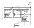
- FIG. 1 shows an example of a functional block of the operation model 100 according to the first embodiment of the present disclosure.
- the operation model 100 corresponds to a specific example of a part of the "logic simulation device" of the present disclosure or a specific example of a part of the "logic simulation program".
- the operation model 100 is provided between the two terminals (bit line BL and source line SL).
- the operation model 100 is a model in which a resistance change type memory element is represented by a logic element.
- the operation model 100 includes, for example, a resistance change type memory element 110 and a truth table 120.
- the resistance change type memory element 110 is composed of hardware that realizes the function of the resistance change type memory element 110, and is the truth.
- the value table 120 is stored in, for example, a volatile memory such as a DRAM (Dynamic Random Access Memory), or a non-volatile memory such as an EEPROM (Electrically Erasable Programmable Read-Only Memory) or a flash memory.
- the operation model 100 may be used in a volatile memory such as a DRAM or a non-volatile memory such as an EEPROM or a flash memory.
- a volatile memory such as a DRAM or a non-volatile memory such as an EEPROM or a flash memory.
- the CPU Central Processing Unit
- the resistance change type memory element 110 is provided between the bit line BL and the source line SL.
- the resistance change type memory element 110 has, for example, a write operation unit 111, a data holding unit 112, and a read operation unit 113.
- the writing operation unit 111 controls data writing to the data holding unit 112.
- the writing operation unit 111 includes, for example, a writing determination unit 111A, as shown in FIG.
- the bit line BL and the source line SL are connected to the write determination unit 111A.
- the write determination unit 111A determines whether to write data to the data holding unit 112 (register unit 112A described later) based on the signal values input to the bit line BL and the source line SL and the truth table 120. ..
- the write determination unit 111A determines that the data is written to the data holding unit 112 (register unit 112A) based on the data input to the bit line BL and the source line SL and the truth value table 120, the source The control signal Trg1 for writing the signal value input to the line SL to the data holding unit 112 (register unit 112A) is output to the data holding unit 112 (register unit 112A).
- FIG. 2 shows a specific example of the truth table 120.
- the truth table 120 is data defining the relationship between the signal values of the bit line BL and the source line SL, data writing to the register unit 112A, and data reading from the register unit 112A.
- three types of operation modes of "1 write” operation, "0 write” operation, and "read” operation are defined.
- the write determination unit 111A determines, for example, that the "0 write” operation is specified when the signal value of the source line SL is "0" and the signal value of the bit line BL is "1".
- the write determination unit 111A determines that the "read” operation is specified when, for example, the signal value of the source line SL is "Hi-z" and the signal value of the bit line BL is "0".
- the control signal Trg1 is not output to the register unit 112A, and for example, the register unit 112A outputs a constant voltage lower than the threshold value used for detecting the control signal Trg1.
- the data holding unit 112 holds the signal value of the source line SL according to the control by the write determination unit 111A.
- the data holding unit 112 includes, for example, a register unit 112A, as shown in FIG.
- the source line SL is connected to the register unit 112A.
- the register unit 112A receives the signal value of the source line SL by using the control signal Trg1 input from the write determination unit 111A as a trigger, and stores it as a register value.
- the register unit 112A outputs "Hi-z" to the read operation unit 113 during the "1 write” operation or the "0 write” operation.
- the register unit 112A outputs a register value to the read operation unit 113 during the “read” operation.
- the read operation unit 113 includes, for example, an output switch 113A and a read determination unit 113B, as shown in FIG.
- the output switch 113A is connected to the output end of the register unit 112A and the source line SL, and connects the output end of the register unit 112A and the source line SL according to the control signal Trg2 from the read determination unit 113B.
- the read determination unit 113B controls reading data to the source line SL.
- the bit line BL and the source line SL are connected to the read determination unit 113B.
- the read determination unit 113B determines whether to read data from the register unit 112A to the source line SL based on the signal values input to the bit line BL and the source line SL and the truth table 120.
- the read determination unit 113B determines the register value from the register unit 112A to the source line SL.
- the control signal Trg2 for reading is output to the output switch 113A.
- the output switch 113A connects the output end of the register unit 112A and the source line SL.
- the read determination unit 113B determines which of the plurality of operation modes specified in the truth table 120 corresponds to the data (signal value) input to the bit line BL and the source line SL. As a result, the read determination unit 113B performs control according to the corresponding operation mode to the output switch 113A.
- the read determination unit 113B determines that the operation is "1 write” and outputs the output.
- the control signal Trg2 for turning off the switch 113A is output to the output switch 113A.
- the output end of the register unit 112A (the output end of the resistance change type memory element 110) is open with respect to the source line SL.
- the read determination unit 113B determines that the operation is "0 write” and outputs the output.
- the control signal Trg2 for turning off the switch 113A is output to the output switch 113A.
- the output end of the register unit 112A (the output end of the resistance change type memory element 110) is open with respect to the source line SL.
- the read determination unit 113B determines that the operation is "read”.
- the control signal Trg2 for turning on the output switch 113A is output to the output switch 113A.
- the output end of the register unit 112A (the output end of the resistance change type memory element 110) is connected to the source line SL.
- the register value (“1” or “0”) held in the register unit 112A is read out to the source line SL.
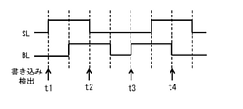
- FIG. 3 shows an example of a signal waveform in the operation model 100.
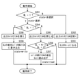
- FIG. 4 shows an example of the operation in the operation model 100.
- the operation model 100 determines whether or not the exclusive OR of the signal value of the source line SL and the signal value of the bit line BL is “1” (step S101). As a result, when the exclusive OR is "1", the operation model 100 opens the output switch 113A (step S102). At this time, the operation model 100 writes the signal value of the source line SL to the register unit 112A (step S103). On the other hand, when the above exclusive OR is not 1, the operation model 100 closes the output switch 113A (step S104).
- the operation model 100 determines whether or not the signal value of the source line SL is "Hi-z” and the signal value of the bit line BL is "0" (step S105). As a result, when the signal value of the source line SL is not “Hi-z” or the signal value of the bit line BL is not “0", the operation model 100 ends the operation. On the other hand, when the signal value of the source line SL is "Hi-z” and the signal value of the bit line BL is "0", the operation model 100 sources the value (register value) of the register unit 112A. Read to the line SL (step S106), and end the operation.
- the determination of data writing and data reading is performed based on the signal values input to the bit line BL and the source line SL and the truth table 120.
- the logic simulation it is possible to reproduce the data writing to the resistance change type memory element and the data reading from the resistance change type memory element.
- the signal input to the source line SL The value is written to the register unit 112A as a register value.
- a signal collision unlike a resistance logic element does not occur. Therefore, in the logic simulation, it is possible to reproduce the data writing to the resistance change type memory element.
- the register held in the register unit 112A is held.
- the value is output to the source line SL.
- the selection unit 112B may be provided in the data holding unit 112.
- the selection unit 112B controls the signal value input to the register unit 112A.
- the source line SL and the output end of the register unit 112A are connected to the selection unit 112B.
- the selection unit 112B controls the signal value to be input to the register unit 112A based on the signal value of the source line SL and the output value of the register unit 112A.
- the selection unit 112B controls either the signal value of the source line SL or the output value of the register unit 112A as a signal value to be input to the register unit 112A by the control signal Trg1 input from the write determination unit 111A. For example, when the source line SL is selected by the control signal Trg1, the selection unit 112B inputs (writes) the signal value of the source line SL to the register unit 112A. For example, when the output value of the register unit 112A is selected, the selection unit 112B inputs (writes) the signal value of the output of the register unit 112A to the register unit 112A.
- the selection unit 112B receives, for example, the signal value of the source line SL and the output value of the register unit 112A, triggered by the control signal Trg1 input from the write determination unit 111A, and registers based on the two received values.
- the signal value input to the unit 112A is controlled. For example, when the signal value of the source line SL and the output value of the register unit 112A are different from each other, the selection unit 112B inputs (writes) the signal value of the source line SL to the register unit 112A. For example, when the signal value of the source line SL and the output value of the register unit 112A are equal to each other, the selection unit 112B does not input (write) to the register unit 112A. As a result, writing to the register unit 112A is omitted.
- the write determination unit 111A not only determines whether data is written, but also determines whether or not there is a change in the signal value of either the source line SL or the bit line BL.
- the write determination unit 111A determines that there is a change in the signal value of either the source line SL or the bit line BL
- the write determination unit 111A outputs a control signal Trg3 for controlling data writing to the register unit 112A to the register unit 112A. do.
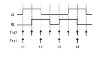
- FIG. 6 shows an example of a signal waveform in the operation model 100 according to this modification.
- the signal value of the source line SL changes periodically from “0” ⁇ “1” ⁇ “0” ⁇ “1”, and the signal value of the bit line BL changes from “0” ⁇ “1” ⁇ “0” ⁇ “1". It is assumed that the signal value of the source line SL changes by half a cycle with respect to the cycle. For example, when the signal value of the bit line BL is "0", "1 write” is detected by the write determination unit 111A at the timing (t1) when the signal value of the source line SL changes from “0” to “1". ..
- control signal Trg1 is output from the write determination unit 111A to the selection unit 112B, and the control signal Trg3 is output from the write determination unit 111A to the register unit 112A.
- the signal value of the source line SL is output from the selection unit 112B to the register unit 112A, and the signal value of the source line SL is written to the register unit 112A.
- the control signal Trg1 is output from the write determination unit 111A to the selection unit 112B, and the control signal Trg3 is output from the write determination unit 111A to the register unit 112A.
- the signal value of the source line SL is output from the selection unit 112B to the register unit 112A, and the signal value of the source line SL is written to the register unit 112A.
- the control signal Trg1 is output from the write determination unit 111A to the selection unit 112B, and the control signal Trg3 is output from the write determination unit 111A to the register unit 112A.
- the signal value of the source line SL is output from the selection unit 112B to the register unit 112A, and the signal value of the source line SL is written to the register unit 112A.
- the control signal Trg1 is output from the write determination unit 111A to the selection unit 112B, and the control signal Trg3 is output from the write determination unit 111A to the register unit 112A.
- the signal value of the source line SL is output from the selection unit 112B to the register unit 112A, and the signal value of the source line SL is written to the register unit 112A.
- the source line SL and the bit line BL may be reversed.
- the source line SL and the bit line BL may be reversed.
- the truth table 121 is provided instead of the truth table 120.
- FIG. 8 shows a specific example of the truth table 121.
- the truth table 121 is data defining the relationship between the signal values of the bit line BL and the source line SL, data writing to the register unit 112A, and data reading from the register unit 112A.
- three types of operation modes of "1 write” operation, "0 write” operation, and "read” operation are defined.
- the write determination unit 111A determines which of the plurality of operation modes specified in the truth table 121 corresponds to the data (signal value) input to the bit line BL and the source line SL. As a result, the write determination unit 111A performs control according to the corresponding operation mode to the data holding unit 112 (register unit 112A).
- the write determination unit 111A determines, for example, that the "1 write” operation is specified when the signal value of the source line SL is "1" and the signal value of the bit line BL is "0".
- the write determination unit 111A determines, for example, that the "0 write” operation is specified when the signal value of the source line SL is "0" and the signal value of the bit line BL is "1".
- the write determination unit 111A determines that the "read” operation is specified when, for example, the signal value of the source line SL is "0” and the signal value of the bit line BL is "Hi-z". However, the control signal Trg1 is not output to the register unit 112A, and for example, the register unit 112A outputs a constant voltage lower than the threshold value used for detecting the control signal Trg1.
- the output switch 113A is connected to the output end of the register unit 112A and the bit line BL, and is connected to the register unit according to the control signal Trg2 from the read determination unit 113B.
- the output end of 112A and the bit line BL are connected and disconnected.
- the read determination unit 113B controls data reading to the bit line BL.
- the bit line BL and the source line SL are connected to the read determination unit 113B.
- the read determination unit 113B determines whether to read data from the register unit 112A to the bit line BL based on the signal values input to the bit line BL and the source line SL and the truth table 121.
- the read determination unit 113B determines the register value from the register unit 112A to the bit line BL.
- the control signal Trg2 for reading is output to the output switch 113A.
- the output switch 113A connects the output end of the register unit 112A and the bit line BL.
- the read determination unit 113B determines which of the plurality of operation modes specified in the truth table 121 corresponds to the data (signal value) input to the bit line BL and the source line SL. As a result, the read determination unit 113B performs control according to the corresponding operation mode to the output switch 113A.
- the read determination unit 113B determines that the operation is "1 write” and outputs the output.
- the control signal Trg2 for turning off the switch 113A is output to the output switch 113A.
- the output end of the register unit 112A (the output end of the resistance change type memory element 110) is open to the bit line BL.
- the read determination unit 113B determines that the operation is "0 write” and outputs the output.
- the control signal Trg2 for turning off the switch 113A is output to the output switch 113A.
- the output end of the register unit 112A (the output end of the resistance change type memory element 110) is open to the bit line BL.
- the read determination unit 113B determines that the operation is "read”.
- the control signal Trg2 for turning on the output switch 113A is output to the output switch 113A.
- the output end of the register unit 112A (the output end of the resistance change type memory element 110) is connected to the bit line BL.
- the register value (“1” or “0”) held in the register unit 112A is read out to the bit line BL.
- FIG. 9 shows an example of a functional block of the operation model 200 according to the second embodiment of the present disclosure.
- the operation model 200 corresponds to a specific example of a part of the "logic simulation device" of the present disclosure or a specific example of a part of the "logic simulation program".
- the operation model 200 is provided between the two terminals (bit line BL and source line SL) as in the above embodiment.
- the operation model 200 is a model in which a resistance change type memory element is represented by a logic element.
- the operation model 200 is connected to a control terminal (word line WL) different from the two terminals (bit line BL and source line SL), and depends on the signal value of the word line WL.
- the selected state of writing or reading data and the non-selected state of the resistance change type memory element are controlled. For example, when the signal value of the word line WL is "1", either data writing or data reading is performed, and when the signal value of the word line WL is "0", the resistance change type memory element is not. It is a choice, and neither data writing nor data reading is performed.
- the operation model 200 includes, for example, a resistance change type memory element 210 and a truth table 220, as shown in FIG.
- the resistance change type memory element 210 is composed of hardware that realizes the function of the resistance change type memory element 210, and is the truth.
- the value table 220 is stored in, for example, a volatile memory such as DRAM or a non-volatile memory such as EEPROM or flash memory.
- the operation model 200 may be used in a volatile memory such as a DRAM or a non-volatile memory such as an EEPROM or a flash memory.
- a volatile memory such as a DRAM or a non-volatile memory such as an EEPROM or a flash memory.
- the resistance change type memory element 210 is provided between the bit line BL and the source line SL.
- the resistance change type memory element 210 has, for example, a write operation unit 211, a data holding unit 212, and a read operation unit 213.
- the writing operation unit 211 controls data writing to the data holding unit 212.
- the write operation unit 211 includes, for example, the write determination unit 211A, as shown in FIG. A bit line BL, a source line SL, and a word line WL are connected to the write determination unit 211A.
- the write determination unit 211A writes data to the data holding unit 212 (register unit 212A described later) based on the signal values input to the bit line BL, the source line SL, and the word line WL, and the truth table 220. Make a judgment.
- the write determination unit 211A determines that the data is written to the data holding unit 212 (register unit 212A) based on the data input to the bit line BL, the source line SL, and the word line WL, and the truth value table 220. At this time, the control signal Trg1 for writing the signal value input to the source line SL to the data holding unit 212 (register unit 212A) is output to the data holding unit 212 (register unit 212A).
- FIG. 10 shows a specific example of the truth table 220.
- the truth table 220 is data defining the relationship between the signal values of the bit line BL, the source line SL, and the word line WL, and the data writing to the register unit 212A and the data reading from the register unit 212A.
- four types of operation modes of "1 write” operation, "0 write” operation, "read” operation, and "non-selection” operation are defined.
- the signal value of the source line SL is “1"
- the signal value of the bit line BL is “0”
- the signal value of the word line WL is "1”.
- "Hi-z” is output from the resistance change type memory element 210 to the source line SL.
- the signal value of the source line SL is "Hi-z"
- the signal value of the bit line BL is "0”
- the signal value of the word line WL is "1”.
- it is specified to read “1” or “0” as the register value from the register unit 212A.
- the register value (“1” or "0") is read from the resistance change type memory element 210 to the source line SL.
- the write determination unit 211A determines which of the plurality of operation modes specified in the truth table 220 corresponds to the data (signal value) input to the bit line BL, the source line SL, and the word line WL. As a result, the write determination unit 211A performs control according to the corresponding operation mode to the data holding unit 212 (register unit 212A). In the write determination unit 211A, for example, the signal value of the source line SL is "1", the signal value of the bit line BL is "0", and the signal value of the word line WL is "1".
- the signal value of the source line SL is "Hi-z"
- the signal value of the bit line BL is "0”
- the signal value of the word line WL is "1”.
- the register unit 212A outputs a constant voltage lower than the threshold value used for detecting the control signal Trg1. do.
- the write determination unit 211A determines that the "non-selection" operation is specified, and does not output the control signal Trg1 to the register unit 212A, for example.
- the register unit 212A outputs a constant voltage lower than the threshold value used for detecting the control signal Trg1.
- the data holding unit 212 holds the signal value of the source line SL according to the control by the write determination unit 211A.
- the data holding unit 212 includes, for example, the register unit 212A, as shown in FIG.
- the source line SL is connected to the register portion 212A.
- the register unit 212A receives the signal value of the source line SL by using the control signal Trg1 input from the write determination unit 211A as a trigger, and stores it as a register value.
- the register unit 212A outputs "Hi-z" to the read operation unit 213 during the "1 write” operation or the "0 write” operation.
- the register unit 212A outputs a register value to the read operation unit 213 during the “read” operation.
- the register unit 212A outputs "Hi-z" to the read operation unit 213 during the "non-selection" operation.
- the read operation unit 213 is configured to include, for example, an output switch 213A and a read determination unit 213B, as shown in FIG.
- the output switch 213A is connected to the output end of the register unit 212A and the source line SL, and connects the output end of the register unit 212A and the source line SL in response to the control signal Trg2 from the read determination unit 213B.
- the read determination unit 213B controls reading data to the source line SL.
- a bit line BL, a source line SL, and a word line WL are connected to the read determination unit 213B.
- the read determination unit 213B determines the data read from the register unit 212A to the source line SL based on the signal values input to the bit line BL, the source line SL, and the word line WL, and the truth table 220. ..
- the read determination unit 212A determines from the register unit 212A that the source line SL is specified.
- the control signal Trg2 for reading the register value is output to the output switch 213A.
- the output switch 213A connects the output end of the register unit 212A and the source line SL.
- the read determination unit 213B determines which of the plurality of operation modes specified in the truth table 220 corresponds to the data (signal value) input to the bit line BL, the source line SL, and the word line WL. As a result, the read determination unit 213B performs control according to the corresponding operation mode to the output switch 213A.
- the signal value of the source line SL is "1"
- the signal value of the bit line BL is "0”
- the signal value of the word line WL is "1”.
- the control signal Trg2 for turning off the output switch 213A is output to the output switch 213A.
- the output end of the register unit 212A (the output end of the resistance change type memory element 210) is open with respect to the source line SL.
- the signal value of the source line SL is "0"
- the signal value of the bit line BL is "1”
- the signal value of the word line WL is “1”.
- the control signal Trg2 for turning off the output switch 213A is output to the output switch 213A.
- the output end of the register unit 212A (the output end of the resistance change type memory element 210) is open with respect to the source line SL.
- the signal value of the source line SL is "Hi-z”
- the signal value of the bit line BL is "0”
- the signal value of the word line WL is "1”.
- the control signal Trg2 for turning on the output switch 213A is output to the output switch 213A.
- the output switch 213A since the output switch 213A is turned on, the output end of the register unit 212A (the output end of the resistance change type memory element 210) is connected to the source line SL.
- the register value (“1” or “0”) held in the register unit 212A is read out to the source line SL.
- the read determination unit 213B determines that the operation is "non-selection", and outputs the control signal Trg2 for turning off the output switch 213A to the output switch 213A. Output to.
- the output switch 213A since the output switch 213A is turned off, the output end of the register unit 212A (the output end of the resistance change type memory element 210) is open with respect to the source line SL.
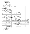
- FIG. 11 shows an example of the operation in the operation model 200.
- the operation model 200 determines whether or not the signal value of the word line WL is “1” (step S201). As a result, when the signal value of the word line WL is not "1", the operation model 200 opens the output switch 113A (step S202). As a result, the signal value of the source line SL becomes Hi-z (step S203), and the operation ends.
- the operation model 200 determines whether or not the exclusive OR of the signal value of the source line SL and the signal value of the bit line BL is "1" (step). S204). As a result, when the above exclusive OR is not “1”, the operation model 200 closes the output switch 113A (step S205). Subsequently, the operation model 200 determines whether or not the signal value of the source line SL is "Hi-z” and the signal value of the bit line BL is "0” (step S206). As a result, when the signal value of the source line SL is not “Hi-z” or the signal value of the bit line BL is not “0", the operation model 200 ends the operation.
- the operation model 200 sources the value (register value) of the register unit 112A. Read to line SL (step S207), and end the operation.
- step S04 when the exclusive OR is "1", the operation model 200 opens the output switch 113A (step S208). Subsequently, the operation model 200 writes the signal value of the source line SL as a register value to the register unit 112A (step S209), and ends the operation.
- data writing, data reading, and non-selection are determined based on the signal values input to the bit line BL, the source line SL, and the word line WL, and the truth table 220.
- the truth table 220 As a result, for example, even when a signal is applied to both ends of the resistance change type memory element 210, a signal collision unlike a resistance logic element does not occur. Therefore, in the logic simulation, it is possible to reproduce the data writing to the resistance change type memory element, the data reading from the resistance change type memory element, and the non-selection of the resistance change type memory element.
- the source line SL when it is determined that data writing is specified based on the signal values input to the bit line BL, the source line SL, and the word line WL and the truth table 220, the source line SL is reached.
- the input signal value is written to the register unit 212A as a register value.
- the register unit 212A when it is determined that data reading is specified based on the signal values input to the bit line BL, the source line SL, and the word line WL and the truth table 220, the register unit 212A is used.
- the held register value is output to the source line SL.
- FIG. 12 shows a modified example of the operation in the operation model 200 according to the second embodiment.
- the operation model 200 determines whether or not the signal value of the word line WL is “1” (step S301). As a result, when the signal value of the word line WL is not "1", the operation model 200 opens the output switch 213A (step S302). As a result, the signal value of the source line SL becomes "Hi-z" (step S303), and the operation ends.
- the operation model 200 (reading determination unit 213B) has elapsed a predetermined time (Read Wait time) from the time when the signal value of the word line WL becomes “1". Wait for it to be done (step S304).
- the operation model 200 determines whether or not the signal value of the source line SL is "Hi-z” and the signal value of the bit line BL is "0" (step S305). ).
- the operation model 200 ends the operation.
- the operation model 200 closes the output switch 213A (step S306). Subsequently, the operation model 200 reads the value (register value) of the register unit 212A to the source line SL (step S307), and ends the operation.
- the operation model 200 determines whether or not the exclusive OR of the signal value of the source line SL and the signal value of the bit line BL is "1" (step S308). .. As a result, when the above exclusive OR is not “1", the operation model 200 ends the operation. On the other hand, when the exclusive OR is "1", the operation model 200 (write determination unit 211A) determines that the exclusive OR is "1" for a predetermined time (Write Wait time). ) Wait for the elapse (step S309).
- the operation model 200 determines whether or not the signal value of the source line SL is "Hi-z” and the signal value of the bit line BL is "0" (step S310). ). As a result, when the signal value of the source line SL is not “Hi-z” or the signal value of the bit line BL is not “0", the operation model 200 ends the operation. On the other hand, when the signal value of the source line SL is "Hi-z” and the signal value of the bit line BL is "0", the operation model 200 opens the output switch 213A (step S311). Subsequently, the operation model 200 writes the signal value of the source line SL as a register value to the register unit 212A (step S312), and ends the operation.
- the timing of outputting the register value held in the register unit 212A to the source line SL is controlled based on the signal value of the word line WL. This makes it possible to reproduce the access time to the register unit 212A at the time of reading.
- the timing of writing to the register unit 212A is controlled based on the signal values of the source line SL and the bit line BL. As a result, the write data is written to the register unit 212A after the write state continues for a certain period of time. As a result, it is possible to avoid a malfunction in which a writing operation occurs due to the accumulation of short pulses.
- FIG. 13 shows a modified example of the operation in the operation model 200 according to the second embodiment.
- the operation model 200 determines whether or not the signal value of the word line WL is “1” (step S401). As a result, when the signal value of the word line WL is not "1", the operation model 200 opens the output switch 213A (step S402). As a result, the signal value of the source line SL becomes "Hi-z" (step S403), and the operation ends.
- the operation model 200 closes the output switch 213A (step S404). Subsequently, the operation model 200 reads the value (register value) of the register unit 212A to the source line SL by Week (step S405), and then the operation model 200 uses the signal value of the source line SL and the signal value of the bit line BL. It is determined whether or not the exclusive OR of is "1" (step S406). As a result, when the above exclusive OR is not "1", the operation model 200 ends the operation. On the other hand, when the exclusive OR is "1", the operation model 200 writes the signal value of the source line SL as a register value to the register unit 212A (step S407), and ends the operation.
- the register value held in the register unit 212A is output to the source line SL by weak. Therefore, in the logic simulation, it is possible to reproduce the data read by the weak from the resistance change type memory element.
- [Modification example E] 14, 15, and 16 show a modification of the functional block of the operation model 200 according to the second embodiment.
- the operation model 200 includes a plurality of resistance conversion type memory elements 210.
- FIG. 14 illustrates a case where the operation model 200 includes two resistance conversion type memory elements 210.
- a set of wiring (source line SL and bit line BL) and a truth table 220 are assigned to each resistance conversion type memory element 210, and a plurality of resistance conversion type memory elements are assigned.
- a common word line WL is assigned to 210.
- FIG. 15 illustrates a case where the operation model 200 includes two resistance conversion type memory elements 210.
- a common set of wiring (source line SL and bit line BL) is assigned to a plurality of resistance conversion type memory elements 210, and further, for each resistance conversion type memory element 210.
- the word line WL and the truth table 220 are assigned.
- FIG. 16 illustrates a case where the operation model 200 includes a plurality of resistance conversion type memory elements 210 arranged in a matrix (m ⁇ n).
- a set of wiring (source line SL and bit line BL) and a truth table 220 are assigned to each of the plurality of resistance conversion type memory elements 210 arranged side by side in the row direction.
- a common word line WL is assigned to a plurality of resistance conversion type memory elements 210 arranged side by side in the row direction.
- a common set of wiring (source line SL and bit line BL) is further assigned to a plurality of resistance conversion type memory elements 210 arranged side by side in the column direction.
- a word line WL is assigned to each of the plurality of resistance conversion type memory elements 210 arranged side by side in the column direction.
- the operation model 200 is provided with a plurality of resistance conversion type memory elements 210. This makes it possible to reproduce the memory cell array in the operation model 200.
- the source line SL and the bit line BL may be reversed.
- the source line SL and the bit line BL may be reversed.
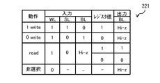
- the truth table 221 is provided instead of the truth table 220.
- FIG. 18 shows a specific example of the truth table 221.
- the truth table 221 is data defining the relationship between the signal values of the bit line BL, the source line SL, and the word line WL, and the data writing to the register unit 212A and the data reading from the register unit 212A. As shown in FIG. 18, for example, the truth table 221 defines four types of operation modes: "1 write” operation, "0 write” operation, "read” operation, and "non-selection" operation.
- the signal value of the bit line BL is "Hi-z"
- the signal value of the source line SL is "0”
- the signal value of the word line WL is "1”.
- the register value (“1” or "0") is read from the resistance change type memory element 210 to the bit line BL.
- the "non-selection” operation is specified to read the register value from the register unit 212A when the signal value of the word line WL is "0". However, when the "read” operation is executed, "Hi-z" is output from the resistance change type memory element 210 to the bit line BL.
- the write determination unit 211A which of the plurality of operation modes specified in the truth table 220 corresponds to the data (signal value) input to the bit line BL, the source line SL, and the word line WL. To judge. As a result, the write determination unit 211A performs control according to the corresponding operation mode to the data holding unit 212 (register unit 212A). In the write determination unit 211A, for example, the signal value of the source line SL is "1", the signal value of the bit line BL is "0", and the signal value of the word line WL is "1".
- the signal value of the bit line BL is "Hi-z"
- the signal value of the source line SL is "0”
- the signal value of the word line WL is "1”.
- the register unit 212A outputs a constant voltage lower than the threshold value used for detecting the control signal Trg1. do.
- the write determination unit 211A determines that the "non-selection" operation is specified, and does not output the control signal Trg1 to the register unit 212A, for example.
- the register unit 212A outputs a constant voltage lower than the threshold value used for detecting the control signal Trg1.
- the output switch 213A is connected to the output end of the register unit 212A and the bit line BL, for example, as shown in FIG. 17, and is connected to the register unit according to the control signal Trg2 from the read determination unit 213B.
- the output end of 212A and the bit line BL are connected and disconnected.
- the read determination unit 213B controls data read to the bit line BL.
- a bit line BL, a source line SL, and a word line WL are connected to the read determination unit 213B.
- the read determination unit 213B determines the data read from the register unit 212A to the bit line BL based on the signal values input to the bit line BL, the source line SL, and the word line WL, and the truth table 221. ..
- the read determination unit 212A determines that the data read is specified, and the bit line BL from the register unit 212A.
- the control signal Trg2 for reading the register value is output to the output switch 213A.
- the output switch 213A connects the output end of the register unit 212A and the bit line BL.
- the read determination unit 213B determines which of the plurality of operation modes specified in the truth table 221 corresponds to the data (signal value) input to the bit line BL, the source line SL, and the word line WL. As a result, the read determination unit 213B performs control according to the corresponding operation mode to the output switch 213A.
- the signal value of the source line SL is "1"
- the signal value of the bit line BL is "0”
- the signal value of the word line WL is "1”.
- the control signal Trg2 for turning off the output switch 213A is output to the output switch 213A.
- the output end of the register unit 212A (the output end of the resistance change type memory element 210) is open with respect to the bit line BL.
- the signal value of the source line SL is "0"
- the signal value of the bit line BL is "1”
- the signal value of the word line WL is “1”.
- the control signal Trg2 for turning off the output switch 213A is output to the output switch 213A.
- the output end of the register unit 212A (the output end of the resistance change type memory element 210) is open with respect to the bit line BL.
- the signal value of the source line SL is "0"
- the signal value of the bit line BL is "Hi-z”
- the signal value of the word line WL is "1”.
- the control signal Trg2 for turning on the output switch 213A is output to the output switch 213A.
- the output switch 213A since the output switch 213A is turned on, the output end of the register unit 212A (the output end of the resistance change type memory element 210) is connected to the bit line BL.
- the register value (“1” or “0”) held in the register unit 212A is read out to the bit line BL.
- the read determination unit 213B determines that the operation is "non-selection", and outputs the control signal Trg2 for turning off the output switch 213A to the output switch 213A. Output to.
- the output switch 213A since the output switch 213A is turned off, the output end of the register unit 212A (the output end of the resistance change type memory element 210) is open with respect to the bit line BL.
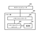
- FIG. 19 shows an example of a functional block of an information processing system to which the operation models 100 and 200 according to each of the above embodiments and modifications thereof are applied.
- This information processing system includes a host computer 300 and a memory unit 400.
- the memory unit 400 includes a memory controller 500, one or more memory cell array units 600, and a power supply unit 700. Note that FIG. 19 illustrates how one memory cell array unit 600 is provided.
- the memory unit 400 corresponds to a specific example of the "logic simulation device" and "logic simulation program" of the present disclosure.
- the host computer 300 controls the memory unit 400. Specifically, the host computer 300 issues a command for designating the logical address of the access destination, and supplies the command and data to the memory unit 400. The host computer 300 receives the data output from the memory unit 400.
- the command is for controlling the memory unit 400, and includes, for example, a write command instructing a data write process and a read command instructing a data read process.
- the logical address is an address assigned to each area of the access unit when the host computer 300 accesses the memory unit 400 in the address space defined by the host computer 300.
- the memory controller 500 controls one or more memory cell array units 600.
- the memory controller 500 receives a write command from the host computer 300 to specify a logical address. Further, the memory controller 500 executes a data writing process according to a write command. In this write process, the logical address is converted into a physical address, and data is written to the physical address.
- the physical address is an address assigned in one or a plurality of memory cell array units 600 for each access unit when the memory controller 500 accesses one or a plurality of memory cell array units 600.
- the memory controller 500 receives a read command for specifying a logical address
- the memory controller 500 converts the logical address into a physical address and reads data from the physical address. Then, the memory controller 500 outputs the read data as read data to the host computer 300.
- the power supply unit 700 supplies a desired voltage to one or a plurality of memory cell array units 600.
- the power supply unit 700 supplies, for example, a voltage used for writing or reading to the row driver 22 described later.
- the power supply unit 700 supplies, for example, a voltage used for writing or reading to the column driver 23 described later.
- FIG. 20 shows an example of a functional block of the memory cell array unit 600.
- the memory cell array unit 600 is composed of, for example, a semiconductor chip.
- the memory cell array unit 600 has, for example, a memory cell array 60 and a drive unit 70.
- the drive unit 70 exchanges commands, write data, read data, and the like with the memory controller 500, for example.
- the drive unit 70 writes data to the memory cell array 60 according to, for example, a write command, and reads data from the memory cell array 60 according to a read command.
- the memory cell array 60 has a plurality of memory cells MC.
- the memory cell MC is configured by, for example, the operation model 200 according to the second embodiment.
- the memory cell array 60 includes, for example, a plurality of word line WLs, a plurality of bit line BLs, a plurality of memory cell MCs arranged one by one at positions where the word line WL and the bit line BL face each other, and a plurality of memory cells MC. It has a source line SL of.
- data can be written to the memory cell MC designated by an address input from the outside.
- the data stored in the memory cell MC designated by the address input can be read out.
- the drive unit 70 includes an address control unit 71, a word line selection unit 72, a command control unit 73, a write control unit 74, a source line / bit line selection unit 75, and a read control unit 76.
- the drive unit 70 includes an address control unit 71, a word line selection unit 72, a command control unit 73, a write control unit 74, a source line / bit line selection unit 75, and a read control unit 76.
- the address control unit 71 outputs a control signal corresponding to the row address input from the address line to the word line selection unit 72, and outputs a control signal according to the column address input from the address line to the source line / bit line selection unit. Output to 75.
- the address control unit 71 outputs a signal for controlling the timing of changing the output voltage to the word line selection unit 72 and the source line / bit line selection unit 75.
- the word line selection unit 72 includes a circuit that drives each word line WL at a predetermined voltage required for the write or read operation when the write or read operation is performed.
- the word line selection unit 72 is connected to each word line WL of the memory cell array 60, and selects the word line WL corresponding to the row address input from the address line.
- the word line selection unit 72 outputs a predetermined voltage required for the write or read operation to the selected word line WL.
- the source line / bit line selection unit 75 includes a circuit that drives the bit line BL and the source line SL connected to the memory cell MC for writing data at a predetermined voltage required for the write operation when the write operation is performed. ..
- the source line / bit line selection unit 75 further drives the bit line BL and the source line SL connected to the memory cell MC for reading data at a predetermined voltage at which data rewriting does not occur when the data reading operation is performed. Includes.
- the source line / bit line selection unit 75 is connected to each bit line BL and each source line SL of the memory cell array 60, and selects the corresponding bit line BL and the source line SL according to the column address input from the address line.
- the source line / bit line selection unit 75 outputs a predetermined voltage required for write or read operation to the selected bit line BL and source line SL.
- the command control unit 73 controls the word line selection unit 72, the write control unit 74, and the read control unit 76 in response to the command input from the memory controller 500.
- the command control unit 73 instructs the write control unit 74 to output the input data Din input from the memory controller 500 to the source line / bit line selection unit 75 at a predetermined timing, and the word line selection unit 72. Is instructed to scan the memory cell array 60 at a predetermined timing.
- the write control unit 74 outputs the input data Din to the source line / bit line selection unit 75 at a predetermined timing.
- the command control unit 73 further instructs the read control unit 76 to read data from the memory cell array 60.
- the read control unit 76 outputs the data read from the memory cell array 60 to the memory controller 500 as output data Dout.
- the operation models 100 and 200 according to each of the above embodiments and variations thereof are applied to the information processing system. This makes it possible to reproduce data writing to the resistance change type memory element and data reading from the resistance change type memory element in the logic simulation.
- data writing and data reading are determined based on the signal values input to the two terminals and the truth table. Therefore, for example, even when a signal is applied to both ends of the resistance change type memory element, signal collision unlike a resistance logic element does not occur. Therefore, it is possible to reproduce the data writing to the resistance change type memory element and the data reading from the resistance change type memory element.
- the present disclosure may have the following structure.
- the operation model is A register for holding data and A truth table that defines the relationship between the signal values of the two terminals and the relationship between writing data to the register and reading data from the register.
- a logic simulation apparatus having a determination unit that makes a determination about the data writing and the data reading based on the signal values input to the two terminals and the truth table.
- the determination unit determines that the data writing is specified based on the signal value input to the two terminals and the truth table, the determination unit is input to one of the two terminals.
- the logic simulation apparatus according to (1), wherein the signal value is written to the register unit as a register value.
- a truth table that defines the relationship between the signal values of the two terminals, writing data to the register unit for holding data, and reading data from the register unit, and a signal input to the two terminals.
- a logic simulation program that causes a computer to make decisions about writing data and reading data based on values.
Landscapes
- Engineering & Computer Science (AREA)
- Theoretical Computer Science (AREA)
- Physics & Mathematics (AREA)
- General Engineering & Computer Science (AREA)
- General Physics & Mathematics (AREA)
- Computer Hardware Design (AREA)
- Human Computer Interaction (AREA)
- Evolutionary Computation (AREA)
- Geometry (AREA)
- Logic Circuits (AREA)
- Semiconductor Memories (AREA)
Abstract
本開示の一側面に係る論理シミュレーション装置は、2つの端子の間に設けられた抵抗変化型メモリ素子の動作モデルを備えている。動作モデルは、データを保持するためのレジスタ部と、真理値表と、判断部とを有している。真理値表では、2つの端子の信号値と、レジスタ部へのデータ書き込みおよびレジスタ部からのデータ読み出しとの関係が規定されている。判断部は、2つの端子へ入力された信号値と、真理値表とに基づいて、データ書き込みおよびデータ読み出しについての判断を行う。
Description
本開示は、論理シミュレーション装置および論理シミュレーションプログラムに関する。
複数の抵抗変化型メモリ素子を含むメモリ回路を設計する際には、指定されたアドレスの抵抗変化型メモリ素子への正しいアクセスを検証するために、メモリ回路をモデル化したシミュレーションが行われる(例えば、特許文献1参照)。
ところで、論理シミュレーション装置では、抵抗変化型メモリ素子を抵抗の論理素子で表現した場合、抵抗変化型メモリ素子の信号レベルを0と1の2状態でしか表現できない。そのため、抵抗変化型メモリ素子へのデータ書き込みや、抵抗変化型メモリ素子からのデータ読出しを再現することができないという問題があった。従って、抵抗変化型メモリ素子へのデータ書き込みや、抵抗変化型メモリ素子からのデータ読出しを再現することの可能な論理シミュレーション装置および論理シミュレーションプログラムを提供することが望ましい。
本開示の一側面に係る論理シミュレーション装置は、2つの端子の間に設けられた抵抗変化型メモリ素子の動作モデルを備えている。この動作モデルは、データを保持するためのレジスタ部と、真理値表と、判断部とを有している。真理値表では、2つの端子の信号値と、レジスタ部へのデータ書き込みおよびレジスタ部からのデータ読み出しとの関係が規定されている。判断部は、2つの端子へ入力された信号値と、真理値表とに基づいて、データ書き込みおよびデータ読み出しについての判断を行う。
本開示の一側面に係る論理シミュレーションプログラムは、2つの端子の間に設けられた抵抗変化型メモリ素子の論理シミュレーションプログラムであって、2つの端子の信号値と、データを保持するためのレジスタ部へのデータ書き込みおよびレジスタ部からのデータ読み出しとの関係について規定された真理値表と、2つの端子へ入力された信号値とに基づいて、データ書き込みおよびデータ読み出しについての判断を行うことをコンピュータに実行させる。
本開示の一側面に係る論理シミュレーション装置および論理シミュレーションプログラムでは、2つの端子へ入力された信号値と、真理値表とに基づいて、データ書き込みおよびデータ読み出しについての判断が行われる。これにより、例えば、抵抗変化型メモリ素子の両端に信号を印可した場合であっても、抵抗の論理素子のような信号衝突が生じることがない。
以下、本開示を実施するための形態について、図面を参照して詳細に説明する。なお、本明細書および図面において、実質的に同一の機能構成を有する構成要素については、同一の符号を付することにより重複説明を省略する。
1.第1の実施の形態(動作モデル)
BLとSLとの間に抵抗変化型メモリ素子を設けた例…図1~図4
2.第1の実施の形態の変形例(動作モデル)
変形例A:データ保持部に選択部を設けた例…図5,図6
変形例B:BLとSLを逆にした例…図7,図8
3.第2の実施の形態(動作モデル)
WLを更に設けた例…図9~図11
4.第2の実施の形態の変形例(動作モデル)
変形例C:書き込み・読出しに待ち時間を設けた例…図12
変形例D:Weakで出力する例…図13
変形例E:複数の抵抗変化素子を設けた例…図14~図16
変形例F:BLとSLを逆にした例…図17,図18
5.適用例(情報処理システム)
上記動作モデルを情報処理システムに適用した例…図19,図20
1.第1の実施の形態(動作モデル)
BLとSLとの間に抵抗変化型メモリ素子を設けた例…図1~図4
2.第1の実施の形態の変形例(動作モデル)
変形例A:データ保持部に選択部を設けた例…図5,図6
変形例B:BLとSLを逆にした例…図7,図8
3.第2の実施の形態(動作モデル)
WLを更に設けた例…図9~図11
4.第2の実施の形態の変形例(動作モデル)
変形例C:書き込み・読出しに待ち時間を設けた例…図12
変形例D:Weakで出力する例…図13
変形例E:複数の抵抗変化素子を設けた例…図14~図16
変形例F:BLとSLを逆にした例…図17,図18
5.適用例(情報処理システム)
上記動作モデルを情報処理システムに適用した例…図19,図20
<1.第1の実施の形態>
[構成]
図1は、本開示の第1の実施の形態に係る動作モデル100の機能ブロックの一例を表したものである。動作モデル100が、本開示の「論理シミュレーション装置」の一部の一具体例もしくは「論理シミュレーションプログラム」の一部の一具体例に相当する。動作モデル100は、2つの端子(ビット線BLおよびソース線SL)の間に設けられる。動作モデル100は、抵抗変化型メモリ素子が論理素子で表現されたモデルである。動作モデル100は、例えば、図1に示したように、抵抗変化型メモリ素子110と、真理値表120とを備える。
[構成]
図1は、本開示の第1の実施の形態に係る動作モデル100の機能ブロックの一例を表したものである。動作モデル100が、本開示の「論理シミュレーション装置」の一部の一具体例もしくは「論理シミュレーションプログラム」の一部の一具体例に相当する。動作モデル100は、2つの端子(ビット線BLおよびソース線SL)の間に設けられる。動作モデル100は、抵抗変化型メモリ素子が論理素子で表現されたモデルである。動作モデル100は、例えば、図1に示したように、抵抗変化型メモリ素子110と、真理値表120とを備える。
動作モデル100が本開示の「論理シミュレーション装置」の一部の一具体例に相当する場合、抵抗変化型メモリ素子110は、抵抗変化型メモリ素子110の機能を実現するハードウェアによって構成され、真理値表120は、例えば、DRAM(Dynamic Random Access Memory)などの揮発性メモリ、または、EEPROM(Electrically Erasable Programmable Read-Only Memory)やフラッシュメモリなどの不揮発性メモリに格納される。動作モデル100が本開示の「論理シミュレーションプログラム」の一部の一具体例に相当する場合、動作モデル100は、例えば、DRAMなどの揮発性メモリ、または、EEPROMやフラッシュメモリなどの不揮発性メモリに格納され、CPU(Central Processing Unit)に動作モデル100がロードされることにより、CPUが動作モデル100の機能を実現する。
抵抗変化型メモリ素子110は、ビット線BLおよびソース線SLの間に設けられる。抵抗変化型メモリ素子110は、例えば、書き込み動作部111、データ保持部112および読み出し動作部113を有する。
書き込み動作部111は、データ保持部112へのデータ書き込みを制御する。書き込み動作部111は、例えば、図1に示したように、書き込み判断部111Aを含んで構成される。書き込み判断部111Aには、ビット線BLおよびソース線SLが接続される。書き込み判断部111Aは、ビット線BLおよびソース線SLへ入力された信号値と、真理値表120とに基づいて、データ保持部112(後述のレジスタ部112A)へのデータ書き込みについての判断を行う。書き込み判断部111Aは、ビット線BLおよびソース線SLへ入力されたデータと、真理値表120とに基づいて、データ保持部112(レジスタ部112A)へのデータ書き込みであると判断したとき、ソース線SLへ入力された信号値をデータ保持部112(レジスタ部112A)へ書き込むための制御信号Trg1をデータ保持部112(レジスタ部112A)へ出力する。
図2は、真理値表120の一具体例を表したものである。真理値表120は、ビット線BLおよびソース線SLの信号値と、レジスタ部112Aへのデータ書き込みおよびレジスタ部112Aからのデータ読み出しとの関係について規定されたデータである。真理値表120には、例えば、図2に示したように、「1write」動作、「0write」動作および「read」動作の3種類の動作モードが規定される。
「1write」動作には、ソース線SLの信号値が「1」となっており、ビット線BLの信号値が「0」となっているとき、レジスタ部112Aにレジスタ値として「1」を書き込むことが規定される。「1write」動作が実行されたとき、抵抗変化型メモリ素子110からソース線SLに「Hi-z」(ハイインピーダンスに相当する値)が出力される。
「0write」動作には、ソース線SLの信号値が「0」となっており、ビット線BLの信号値が「1」となっているとき、レジスタ部112Aにレジスタ値として「0」を書き込むことが規定される。「0write」動作が実行されたとき、抵抗変化型メモリ素子110からソース線SLに「Hi-z」が出力される。
「read」動作には、ソース線SLの信号値が「Hi-z」となっており、ビット線BLの信号値が「0」となっているとき、レジスタ部112Aからレジスタ値として「1」または「0」を読み出すことが規定される。「read」動作が実行されたとき、抵抗変化型メモリ素子110からソース線SLにレジスタ値(「1」または「0」)が読み出される。
書き込み判断部111Aは、ビット線BLおよびソース線SLへ入力されたデータ(信号値)が真理値表120に規定された複数の動作モードのいずれに該当するかを判断する。書き込み判断部111Aは、その結果、該当した動作モードに応じた制御をデータ保持部112(レジスタ部112A)に対して行う。書き込み判断部111Aは、例えば、ソース線SLの信号値が「1」となっており、ビット線BLの信号値が「0」となっているとき、「1write」動作が指定されたと判断し、レジスタ部112Aにレジスタ値としてソース線SLへ入力されたデータ(信号値)(=「1」)を書き込むための制御信号Trg1をレジスタ部112Aに出力する。書き込み判断部111Aは、例えば、ソース線SLの信号値が「0」となっており、ビット線BLの信号値が「1」となっているとき、「0write」動作が指定されたと判断し、レジスタ部112Aにレジスタ値としてソース線SLへ入力されたデータ(信号値)(=「0」)を書き込むための制御信号Trg1をレジスタ部112Aに出力する。書き込み判断部111Aは、例えば、ソース線SLの信号値が「Hi-z」となっており、ビット線BLの信号値が「0」となっているとき、「read」動作が指定されたと判断し、制御信号Trg1をレジスタ部112Aに出力せず、例えば、レジスタ部112Aにおいて制御信号Trg1の検出に用いられる閾値よりも低い定電圧を出力する。
データ保持部112は、書き込み判断部111Aによる制御に従って、ソース線SLの信号値を保持する。データ保持部112は、例えば、図1に示したように、レジスタ部112Aを含んで構成される。レジスタ部112Aには、ソース線SLが接続される。レジスタ部112Aは、書き込み判断部111Aから入力される制御信号Trg1をトリガとして、ソース線SLの信号値を受け取り、レジスタ値として記憶する。レジスタ部112Aは、「1write」動作、または、「0write」動作のとき、読み出し動作部113に対して、「Hi-z」を出力する。レジスタ部112Aは、「read」動作のとき、読み出し動作部113に対して、レジスタ値を出力する。
読み出し動作部113は、例えば、図1に示したように、出力スイッチ113Aおよび読み出し判断部113Bを含んで構成される。出力スイッチ113Aは、レジスタ部112Aの出力端とソース線SLとに接続され、読み出し判断部113Bからの制御信号Trg2に応じて、レジスタ部112Aの出力端とソース線SLとの継断を行う。
読み出し判断部113Bは、ソース線SLへのデータ読み出しを制御する。読み出し判断部113Bには、ビット線BLおよびソース線SLが接続される。読み出し判断部113Bは、ビット線BLおよびソース線SLへ入力された信号値と、真理値表120とに基づいて、レジスタ部112Aからソース線SLへのデータ読み出しについての判断を行う。読み出し判断部113Bは、ビット線BLおよびソース線SLへ入力されたデータと、真理値表120とに基づいて、データ読み出しが指定されたと判断したとき、レジスタ部112Aからソース線SLへレジスタ値を読み出すための制御信号Trg2を出力スイッチ113Aへ出力する。出力スイッチ113Aは、読み出し判断部113Bから、レジスタ値を読み出すための制御信号Trg2が入力されると、レジスタ部112Aの出力端とソース線SLとを接続する。
読み出し判断部113Bは、ビット線BLおよびソース線SLへ入力されたデータ(信号値)が真理値表120に規定された複数の動作モードのいずれに該当するかを判断する。読み出し判断部113Bは、その結果、該当した動作モードに応じた制御を出力スイッチ113Aに対して行う。
読み出し判断部113Bは、例えば、ソース線SLの信号値が「1」となっており、ビット線BLの信号値が「0」となっているとき、「1write」動作であると判断し、出力スイッチ113Aをオフするための制御信号Trg2を出力スイッチ113Aに出力する。このとき、出力スイッチ113Aはオフとなるので、レジスタ部112Aの出力端(抵抗変化型メモリ素子110の出力端)は、ソース線SLに対してオープンとなる。
読み出し判断部113Bは、例えば、ソース線SLの信号値が「0」となっており、ビット線BLの信号値が「1」となっているとき、「0write」動作であると判断し、出力スイッチ113Aをオフするための制御信号Trg2を出力スイッチ113Aに出力する。このとき、出力スイッチ113Aはオフとなるので、レジスタ部112Aの出力端(抵抗変化型メモリ素子110の出力端)は、ソース線SLに対してオープンとなる。
読み出し判断部113Bは、例えば、ソース線SLの信号値が「Hi-z」となっており、ビット線BLの信号値が「0」となっているとき、「read」動作であると判断し、出力スイッチ113Aをオンするための制御信号Trg2を出力スイッチ113Aに出力する。このとき、出力スイッチ113Aはオンとなるので、レジスタ部112Aの出力端(抵抗変化型メモリ素子110の出力端)は、ソース線SLに接続される。その結果、ソース線SLには、レジスタ部112Aに保持されているレジスタ値(「1」または「0」)が読み出される。
図3は、動作モデル100における信号波形の一例を表したものである。ソース線SLの信号値が「0」→「1」→「0」→「1」と周期的に変化し、ビット線BLの信号値が「0」→「1」→「0」→「1」と、ソース線SLの信号値の周期に対して半周期ずれて変化しているとする。例えば、ビット線BLの信号値が「0」のとき、ソース線SLの信号値が「0」から「1」に変化したタイミング(t1)で、「1write」が書き込み判断部111Aによって検出される。このとき、ソース線SLの信号値(=「1」)がレジスタ部112Aに書き込まれる。例えば、ビット線BLの信号値が「1」のとき、ソース線SLの信号値が「1」から「0」に変化したタイミング(t2)で、「0write」が書き込み判断部111Aによって検出される。このとき、ソース線SLの信号値(=「0」)がレジスタ部112Aに書き込まれる。
例えば、ソース線SLの信号値が「0」のとき、ビット線BLの信号値が「0」から「1」に変化したタイミング(t3)で、「0write」が書き込み判断部111Aによって検出される。このとき、ソース線SLの信号値(=「0」)がレジスタ部112Aに書き込まれる。例えば、ソース線SLの信号値が「1」のとき、ビット線BLの信号値が「1」から「0」に変化したタイミング(t4)で、「1write」が書き込み判断部111Aによって検出される。このとき、ソース線SLの信号値(=「1」)がレジスタ部112Aに書き込まれる。
図4は、動作モデル100における動作の一例を表したものである。動作モデル100は、ソース線SLの信号値とビット線BLの信号値との排他的論理和が「1」か否か判断する(ステップS101)。その結果、上記の排他的論理和が「1」のとき、動作モデル100は出力スイッチ113Aを開く(ステップS102)。このとき、動作モデル100は、ソース線SLの信号値をレジスタ部112Aに書き込む(ステップS103)。一方、上記の排他的論理和が1ではないとき、動作モデル100は出力スイッチ113Aを閉じる(ステップS104)。続いて、動作モデル100は、ソース線SLの信号値が「Hi-z」であって、かつ、ビット線BLの信号値が「0」であるか否か判断する(ステップS105)。その結果、ソース線SLの信号値が「Hi-z」ではないか、または、ビット線BLの信号値が「0」ではないときには、動作モデル100は動作を終了する。一方、ソース線SLの信号値が「Hi-z」であって、かつ、ビット線BLの信号値が「0」であるとき、動作モデル100は、レジスタ部112Aの値(レジスタ値)をソース線SLに読み出し(ステップS106)、動作を終了する。
[効果]
次に、動作モデル100の効果について説明する。
次に、動作モデル100の効果について説明する。
複数の抵抗変化型メモリ素子を含むメモリ回路を設計する際には、指定されたアドレスの抵抗変化型メモリ素子への正しいアクセスを検証するために、メモリ回路をモデル化したシミュレーションが行われる。ところで、論理シミュレーション装置では、抵抗変化型メモリ素子を抵抗の論理素子で表現した場合、抵抗変化型メモリ素子の信号レベルを「0」と「1」の2状態でしか表現できない。そのため、抵抗変化型メモリ素子へのデータ書き込みや、抵抗変化型メモリ素子からのデータ読出しを再現することができないという問題があった。
一方、本実施の形態では、ビット線BLおよびソース線SLへ入力された信号値と、真理値表120とに基づいて、データ書き込みおよびデータ読み出しについての判断が行われる。これにより、例えば、抵抗変化型メモリ素子110の両端に信号を印可した場合であっても、抵抗の論理素子のような信号衝突が生じることがない。従って、論理シミュレーションにおいて、抵抗変化型メモリ素子へのデータ書き込みや、抵抗変化型メモリ素子からのデータ読出しを再現することが可能となる。
また、本実施の形態では、ビット線BLおよびソース線SLへ入力された信号値と、真理値表120とに基づいて、データ書き込みが指定されたと判断したとき、ソース線SLへ入力された信号値がレジスタ値としてレジスタ部112Aへ書き込まれる。これにより、例えば、抵抗変化型メモリ素子110の両端に信号を印可した場合であっても、抵抗の論理素子のような信号衝突が生じることがない。従って、論理シミュレーションにおいて、抵抗変化型メモリ素子へのデータ書き込みを再現することが可能となる。
また、本実施の形態では、ビット線BLおよびソース線SLへ入力された信号値と、真理値表120とに基づいて、データ読み出しが指定されたと判断したとき、レジスタ部112Aに保持されたレジスタ値がソース線SLへ出力される。これにより、例えば、抵抗変化型メモリ素子110の両端に信号を印可した場合であっても、抵抗の論理素子のような信号衝突が生じることがない。従って、論理シミュレーションにおいて、抵抗変化型メモリ素子からのデータ読み出しを再現することが可能となる。
<2.第1の実施の形態に係る変形例>
[変形例A]
上記実施の形態において、例えば、図5に示したように、選択部112Bがデータ保持部112に設けられてもよい。選択部112Bは、レジスタ部112Aへ入力する信号値を制御する。選択部112Bには、ソース線SLと、レジスタ部112Aの出力端とが接続される。選択部112Bは、ソース線SLの信号値と、レジスタ部112Aの出力値とに基づいて、レジスタ部112Aへ入力する信号値を制御する。選択部112Bは、書き込み判断部111Aから入力される制御信号Trg1によって、ソース線SLの信号値と、レジスタ部112Aの出力値のどちらかをレジスタ部112Aへ入力する信号値として制御する。例えば、制御信号Trg1によってソース線SLが選択された場合、選択部112Bは、ソース線SLの信号値をレジスタ部112Aへ入力する(書き込む)。例えば、レジスタ部112Aの出力値が選択された場合、選択部112Bは、レジスタ部112Aの出力の信号値をレジスタ部112Aへ入力する(書き込む)。
[変形例A]
上記実施の形態において、例えば、図5に示したように、選択部112Bがデータ保持部112に設けられてもよい。選択部112Bは、レジスタ部112Aへ入力する信号値を制御する。選択部112Bには、ソース線SLと、レジスタ部112Aの出力端とが接続される。選択部112Bは、ソース線SLの信号値と、レジスタ部112Aの出力値とに基づいて、レジスタ部112Aへ入力する信号値を制御する。選択部112Bは、書き込み判断部111Aから入力される制御信号Trg1によって、ソース線SLの信号値と、レジスタ部112Aの出力値のどちらかをレジスタ部112Aへ入力する信号値として制御する。例えば、制御信号Trg1によってソース線SLが選択された場合、選択部112Bは、ソース線SLの信号値をレジスタ部112Aへ入力する(書き込む)。例えば、レジスタ部112Aの出力値が選択された場合、選択部112Bは、レジスタ部112Aの出力の信号値をレジスタ部112Aへ入力する(書き込む)。
選択部112Bは、例えば、書き込み判断部111Aから入力される制御信号Trg1をトリガとして、ソース線SLの信号値と、レジスタ部112Aの出力値とを受け取り、受け取った2つの値に基づいて、レジスタ部112Aへ入力する信号値を制御する。例えば、ソース線SLの信号値と、レジスタ部112Aの出力値とが互いに異なる場合、選択部112Bは、ソース線SLの信号値をレジスタ部112Aへ入力する(書き込む)。例えば、ソース線SLの信号値と、レジスタ部112Aの出力値とが互いに等しい場合、選択部112Bは、レジスタ部112Aへの入力(書き込み)を行わない。これにより、レジスタ部112Aへの書き込みが省略される。
本変形例では、書き込み判断部111Aは、データ書き込みについての判断だけでなく、ソース線SLおよびビット線BLのいずれか一方の信号値に変化があるか否かの判断も行う。書き込み判断部111Aは、ソース線SLおよびビット線BLのいずれか一方の信号値に変化があると判断したとき、レジスタ部112Aへのデータ書き込みを制御するための制御信号Trg3をレジスタ部112Aへ出力する。
図6は、本変形例に係る動作モデル100における信号波形の一例を表したものである。ソース線SLの信号値が「0」→「1」→「0」→「1」と周期的に変化し、ビット線BLの信号値が「0」→「1」→「0」→「1」と、ソース線SLの信号値の周期に対して半周期ずれて変化しているとする。例えば、ビット線BLの信号値が「0」のとき、ソース線SLの信号値が「0」から「1」に変化したタイミング(t1)で、「1write」が書き込み判断部111Aによって検出される。このとき、制御信号Trg1が書き込み判断部111Aから選択部112Bに出力され、制御信号Trg3が書き込み判断部111Aからレジスタ部112Aに出力される。その結果、ソース線SLの信号値が選択部112Bからレジスタ部112Aに出力され、ソース線SLの信号値がレジスタ部112Aに書き込まれる。
例えば、ビット線BLの信号値が「1」のとき、ソース線SLの信号値が「1」から「0」に変化したタイミング(t2)で、「0write」が書き込み判断部111Aによって検出される。このとき、制御信号Trg1が書き込み判断部111Aから選択部112Bに出力され、制御信号Trg3が書き込み判断部111Aからレジスタ部112Aに出力される。その結果、ソース線SLの信号値が選択部112Bからレジスタ部112Aに出力され、ソース線SLの信号値がレジスタ部112Aに書き込まれる。
例えば、ソース線SLの信号値が「0」のとき、ビット線BLの信号値が「0」から「1」に変化したタイミング(t3)で、「0write」が書き込み判断部111Aによって検出される。このとき、制御信号Trg1が書き込み判断部111Aから選択部112Bに出力され、制御信号Trg3が書き込み判断部111Aからレジスタ部112Aに出力される。その結果、ソース線SLの信号値が選択部112Bからレジスタ部112Aに出力され、ソース線SLの信号値がレジスタ部112Aに書き込まれる。
例えば、ソース線SLの信号値が「1」のとき、ビット線BLの信号値が「1」から「0」に変化したタイミング(t4)で、「1write」が書き込み判断部111Aによって検出される。このとき、制御信号Trg1が書き込み判断部111Aから選択部112Bに出力され、制御信号Trg3が書き込み判断部111Aからレジスタ部112Aに出力される。その結果、ソース線SLの信号値が選択部112Bからレジスタ部112Aに出力され、ソース線SLの信号値がレジスタ部112Aに書き込まれる。
このように、本変形例では、上記実施の形態と同様の書き込み制御がなされる。従って、本変形例では、上記実施の形態と同様の効果が得られる。
[変形例B]
上記実施の形態およびその変形例において、ソース線SLとビット線BLとが逆になっていてもよい。例えば、図7に示したように、上記実施の形態において、ソース線SLとビット線BLとが逆になっていてもよい。このとき、真理値表120の代わりに、真理値表121が設けられる。
上記実施の形態およびその変形例において、ソース線SLとビット線BLとが逆になっていてもよい。例えば、図7に示したように、上記実施の形態において、ソース線SLとビット線BLとが逆になっていてもよい。このとき、真理値表120の代わりに、真理値表121が設けられる。
図8は、真理値表121の一具体例を表したものである。真理値表121は、ビット線BLおよびソース線SLの信号値と、レジスタ部112Aへのデータ書き込みおよびレジスタ部112Aからのデータ読み出しとの関係について規定されたデータである。真理値表121には、例えば、図8に示したように、「1write」動作、「0write」動作および「read」動作の3種類の動作モードが規定される。
「1write」動作には、ソース線SLの信号値が「1」となっており、ビット線BLの信号値が「0」となっているとき、レジスタ部112Aにレジスタ値として「1」を書き込むことが規定される。「1write」動作が実行されたとき、抵抗変化型メモリ素子110からビット線BLに「Hi-z」が出力される。
「0write」動作には、ソース線SLの信号値が「0」となっており、ビット線BLの信号値が「1」となっているとき、レジスタ部112Aにレジスタ値として「0」を書き込むことが規定される。「0write」動作が実行されたとき、抵抗変化型メモリ素子110からビット線BLに「Hi-z」が出力される。
「read」動作には、ソース線SLの信号値が「0」となっており、ビット線BLの信号値が「Hi-z」となっているとき、レジスタ部112Aからレジスタ値として「1」または「0」を読み出すことが規定される。「read」動作が実行されたとき、抵抗変化型メモリ素子110からビット線BLにレジスタ値(「1」または「0」)が読み出される。
本変形例では、書き込み判断部111Aは、ビット線BLおよびソース線SLへ入力されたデータ(信号値)が真理値表121に規定された複数の動作モードのいずれに該当するかを判断する。書き込み判断部111Aは、その結果、該当した動作モードに応じた制御をデータ保持部112(レジスタ部112A)に対して行う。書き込み判断部111Aは、例えば、ソース線SLの信号値が「1」となっており、ビット線BLの信号値が「0」となっているとき、「1write」動作が指定されたと判断し、レジスタ部112Aにレジスタ値としてソース線SLへ入力されたデータ(信号値)(=「1」)を書き込むための制御信号Trg1をレジスタ部112Aに出力する。書き込み判断部111Aは、例えば、ソース線SLの信号値が「0」となっており、ビット線BLの信号値が「1」となっているとき、「0write」動作が指定されたと判断し、レジスタ部112Aにレジスタ値としてソース線SLへ入力されたデータ(信号値)(=「0」)を書き込むための制御信号Trg1をレジスタ部112Aに出力する。書き込み判断部111Aは、例えば、ソース線SLの信号値が「0」となっており、ビット線BLの信号値が「Hi-z」となっているとき、「read」動作が指定されたと判断し、制御信号Trg1をレジスタ部112Aに出力せず、例えば、レジスタ部112Aにおいて制御信号Trg1の検出に用いられる閾値よりも低い定電圧を出力する。
本変形例では、出力スイッチ113Aは、例えば、図7に示したように、レジスタ部112Aの出力端とビット線BLとに接続され、読み出し判断部113Bからの制御信号Trg2に応じて、レジスタ部112Aの出力端とビット線BLとの継断を行う。
本変形例では、読み出し判断部113Bは、ビット線BLへのデータ読み出しを制御する。読み出し判断部113Bには、ビット線BLおよびソース線SLが接続される。読み出し判断部113Bは、ビット線BLおよびソース線SLへ入力された信号値と、真理値表121とに基づいて、レジスタ部112Aからビット線BLへのデータ読み出しについての判断を行う。読み出し判断部113Bは、ビット線BLおよびソース線SLへ入力されたデータと、真理値表121とに基づいて、データ読み出しが指定されたと判断したとき、レジスタ部112Aからビット線BLへレジスタ値を読み出すための制御信号Trg2を出力スイッチ113Aへ出力する。出力スイッチ113Aは、読み出し判断部113Bから、レジスタ値を読み出すための制御信号Trg2が入力されると、レジスタ部112Aの出力端とビット線BLとを接続する。
読み出し判断部113Bは、ビット線BLおよびソース線SLへ入力されたデータ(信号値)が真理値表121に規定された複数の動作モードのいずれに該当するかを判断する。読み出し判断部113Bは、その結果、該当した動作モードに応じた制御を出力スイッチ113Aに対して行う。
読み出し判断部113Bは、例えば、ソース線SLの信号値が「1」となっており、ビット線BLの信号値が「0」となっているとき、「1write」動作であると判断し、出力スイッチ113Aをオフするための制御信号Trg2を出力スイッチ113Aに出力する。このとき、出力スイッチ113Aはオフとなるので、レジスタ部112Aの出力端(抵抗変化型メモリ素子110の出力端)は、ビット線BLに対してオープンとなる。
読み出し判断部113Bは、例えば、ソース線SLの信号値が「0」となっており、ビット線BLの信号値が「1」となっているとき、「0write」動作であると判断し、出力スイッチ113Aをオフするための制御信号Trg2を出力スイッチ113Aに出力する。このとき、出力スイッチ113Aはオフとなるので、レジスタ部112Aの出力端(抵抗変化型メモリ素子110の出力端)は、ビット線BLに対してオープンとなる。
読み出し判断部113Bは、例えば、ソース線SLの信号値が「0」となっており、ビット線BLの信号値が「Hi-z」となっているとき、「read」動作であると判断し、出力スイッチ113Aをオンするための制御信号Trg2を出力スイッチ113Aに出力する。このとき、出力スイッチ113Aはオンとなるので、レジスタ部112Aの出力端(抵抗変化型メモリ素子110の出力端)は、ビット線BLに接続される。その結果、ビット線BLには、レジスタ部112Aに保持されているレジスタ値(「1」または「0」)が読み出される。
このように、本変形例では、上記実施の形態と比較すると、読み出す配線が異なるものの、上記実施の形態と同様の書き込み制御および読み出し制御がなされる。従って、本変形例では、上記実施の形態と同様の効果が得られる。
<3.第2の実施の形態>
[構成]
図9は、本開示の第2の実施の形態に係る動作モデル200の機能ブロックの一例を表したものである。動作モデル200が、本開示の「論理シミュレーション装置」の一部の一具体例もしくは「論理シミュレーションプログラム」の一部の一具体例に相当する。動作モデル200は、上記実施の形態と同様、2つの端子(ビット線BLおよびソース線SL)の間に設けられる。動作モデル200は、抵抗変化型メモリ素子が論理素子で表現されたモデルである。動作モデル200は、例えば、図9に示したように、2つの端子(ビット線BLおよびソース線SL)とは異なる制御端子(ワード線WL)に接続されており、ワード線WLの信号値により、データ書き込みもしくはデータ読み出しを行う選択状態と、抵抗変化型メモリ素子の非選択状態とを制御する。例えば、ワード線WLの信号値が「1」のとき、データ書き込みおよびデータ読み出しのいずれか一方の動作が行われ、ワード線WLの信号値が「0」のとき、抵抗変化型メモリ素子が非選択となり、データ書き込みおよびデータ読み出しのいずれも行われない。
[構成]
図9は、本開示の第2の実施の形態に係る動作モデル200の機能ブロックの一例を表したものである。動作モデル200が、本開示の「論理シミュレーション装置」の一部の一具体例もしくは「論理シミュレーションプログラム」の一部の一具体例に相当する。動作モデル200は、上記実施の形態と同様、2つの端子(ビット線BLおよびソース線SL)の間に設けられる。動作モデル200は、抵抗変化型メモリ素子が論理素子で表現されたモデルである。動作モデル200は、例えば、図9に示したように、2つの端子(ビット線BLおよびソース線SL)とは異なる制御端子(ワード線WL)に接続されており、ワード線WLの信号値により、データ書き込みもしくはデータ読み出しを行う選択状態と、抵抗変化型メモリ素子の非選択状態とを制御する。例えば、ワード線WLの信号値が「1」のとき、データ書き込みおよびデータ読み出しのいずれか一方の動作が行われ、ワード線WLの信号値が「0」のとき、抵抗変化型メモリ素子が非選択となり、データ書き込みおよびデータ読み出しのいずれも行われない。
動作モデル200は、例えば、図9に示したように、抵抗変化型メモリ素子210と、真理値表220とを備える。動作モデル200が本開示の「論理シミュレーション装置」の一部の一具体例に相当する場合、抵抗変化型メモリ素子210は、抵抗変化型メモリ素子210の機能を実現するハードウェアによって構成され、真理値表220は、例えば、DRAMなどの揮発性メモリ、または、EEPROMやフラッシュメモリなどの不揮発性メモリに格納される。動作モデル200が本開示の「論理シミュレーションプログラム」の一部の一具体例に相当する場合、動作モデル200は、例えば、DRAMなどの揮発性メモリ、または、EEPROMやフラッシュメモリなどの不揮発性メモリに格納され、CPUに動作モデル200がロードされることにより、CPUが動作モデル200の機能を実現する。
抵抗変化型メモリ素子210は、ビット線BLおよびソース線SLの間に設けられる。抵抗変化型メモリ素子210は、例えば、書き込み動作部211、データ保持部212および読み出し動作部213を有する。
書き込み動作部211は、データ保持部212へのデータ書き込みを制御する。書き込み動作部211は、例えば、図9に示したように、書き込み判断部211Aを含んで構成される。書き込み判断部211Aには、ビット線BL、ソース線SLおよびワード線WLが接続される。書き込み判断部211Aは、ビット線BL、ソース線SLおよびワード線WLへ入力された信号値と、真理値表220とに基づいて、データ保持部212(後述のレジスタ部212A)へのデータ書き込みについての判断を行う。書き込み判断部211Aは、ビット線BL、ソース線SLおよびワード線WLへ入力されたデータと、真理値表220とに基づいて、データ保持部212(レジスタ部212A)へのデータ書き込みであると判断したとき、ソース線SLへ入力された信号値をデータ保持部212(レジスタ部212A)へ書き込むための制御信号Trg1をデータ保持部212(レジスタ部212A)へ出力する。
図10は、真理値表220の一具体例を表したものである。真理値表220は、ビット線BL、ソース線SLおよびワード線WLの信号値と、レジスタ部212Aへのデータ書き込みおよびレジスタ部212Aからのデータ読み出しとの関係について規定されたデータである。真理値表220には、例えば、図10に示したように、「1write」動作、「0write」動作、「read」動作および「非選択」動作の4種類の動作モードが規定される。
「1write」動作には、ソース線SLの信号値が「1」となっており、ビット線BLの信号値が「0」となっており、ワード線WLの信号値が「1」となっているとき、レジスタ部212Aにレジスタ値として「1」を書き込むことが規定される。「1write」動作が実行されたとき、抵抗変化型メモリ素子210からソース線SLに「Hi-z」が出力される。
「0write」動作には、ソース線SLの信号値が「0」となっており、ビット線BLの信号値が「1」なっており、ワード線WLの信号値が「1」となっているとき、レジスタ部212Aにレジスタ値として「0」を書き込むことが規定される。「0write」動作が実行されたとき、抵抗変化型メモリ素子210からソース線SLに「Hi-z」が出力される。
「read」動作には、ソース線SLの信号値が「Hi-z」となっており、ビット線BLの信号値が「0」なっており、ワード線WLの信号値が「1」となっているとき、レジスタ部212Aからレジスタ値として「1」または「0」を読み出すことが規定される。「read」動作が実行されたとき、抵抗変化型メモリ素子210からソース線SLにレジスタ値(「1」または「0」)が読み出される。
「非選択」動作には、ワード線WLの信号値が「0」となっているとき、データ書き込みおよびデータ読み出しのいずれも行われず、ソース線SLが「Hi-z」になる。
書き込み判断部211Aは、ビット線BL、ソース線SLおよびワード線WLへ入力されたデータ(信号値)が真理値表220に規定された複数の動作モードのいずれに該当するかを判断する。書き込み判断部211Aは、その結果、該当した動作モードに応じた制御をデータ保持部212(レジスタ部212A)に対して行う。書き込み判断部211Aは、例えば、ソース線SLの信号値が「1」となっており、ビット線BLの信号値が「0」なっており、ワード線WLの信号値が「1」となっているとき、「1write」動作が指定されたと判断し、レジスタ部212Aにレジスタ値としてソース線SLへ入力されたデータ(信号値)(=「1」)を書き込むための制御信号Trg1をレジスタ部212Aに出力する。書き込み判断部211Aは、例えば、ソース線SLの信号値が「0」となっており、ビット線BLの信号値が「1」なっており、ワード線WLの信号値が「1」となっているとき、「0write」動作が指定されたと判断し、レジスタ部212Aにレジスタ値としてソース線SLへ入力されたデータ(信号値)(=「0」)を書き込むための制御信号Trg1をレジスタ部212Aに出力する。
書き込み判断部211Aは、例えば、ソース線SLの信号値が「Hi-z」となっており、ビット線BLの信号値が「0」なっており、ワード線WLの信号値が「1」となっているとき、「read」動作が指定されたと判断し、制御信号Trg1をレジスタ部212Aに出力せず、例えば、レジスタ部212Aにおいて制御信号Trg1の検出に用いられる閾値よりも低い定電圧を出力する。書き込み判断部211Aは、例えば、ワード線WLの信号値が「0」となっているとき、「非選択」動作が指定されたと判断し、制御信号Trg1をレジスタ部212Aに出力せず、例えば、レジスタ部212Aにおいて制御信号Trg1の検出に用いられる閾値よりも低い定電圧を出力する。
データ保持部212は、書き込み判断部211Aによる制御に従って、ソース線SLの信号値を保持する。データ保持部212は、例えば、図9に示したように、レジスタ部212Aを含んで構成される。レジスタ部212Aには、ソース線SLが接続される。レジスタ部212Aは、書き込み判断部211Aから入力される制御信号Trg1をトリガとして、ソース線SLの信号値を受け取り、レジスタ値として記憶する。レジスタ部212Aは、「1write」動作、または、「0write」動作のとき、読み出し動作部213に対して、「Hi-z」を出力する。レジスタ部212Aは、「read」動作のとき、読み出し動作部213に対して、レジスタ値を出力する。レジスタ部212Aは、「非選択」動作のとき、読み出し動作部213に対して、「Hi-z」を出力する。
読み出し動作部213は、例えば、図9に示したように、出力スイッチ213Aおよび読み出し判断部213Bを含んで構成される。出力スイッチ213Aは、レジスタ部212Aの出力端とソース線SLとに接続され、読み出し判断部213Bからの制御信号Trg2に応じて、レジスタ部212Aの出力端とソース線SLとの継断を行う。
読み出し判断部213Bは、ソース線SLへのデータ読み出しを制御する。読み出し判断部213Bには、ビット線BL、ソース線SLおよびワード線WLが接続される。読み出し判断部213Bは、ビット線BL、ソース線SLおよびワード線WLへ入力された信号値と、真理値表220とに基づいて、レジスタ部212Aからソース線SLへのデータ読み出しについての判断を行う。読み出し判断部213Bは、ビット線BL、ソース線SLおよびワード線WLへ入力されたデータと、真理値表220とに基づいて、データ読み出しが指定されたと判断したとき、レジスタ部212Aからソース線SLへレジスタ値を読み出すための制御信号Trg2を出力スイッチ213Aへ出力する。出力スイッチ213Aは、読み出し判断部213Bから、レジスタ値を読み出すための制御信号Trg2が入力されると、レジスタ部212Aの出力端とソース線SLとを接続する。
読み出し判断部213Bは、ビット線BL、ソース線SLおよびワード線WLへ入力されたデータ(信号値)が真理値表220に規定された複数の動作モードのいずれに該当するかを判断する。読み出し判断部213Bは、その結果、該当した動作モードに応じた制御を出力スイッチ213Aに対して行う。
読み出し判断部213Bは、例えば、ソース線SLの信号値が「1」となっており、ビット線BLの信号値が「0」となっており、ワード線WLの信号値が「1」となっているとき、「1write」動作であると判断し、出力スイッチ213Aをオフするための制御信号Trg2を出力スイッチ213Aに出力する。このとき、出力スイッチ213Aはオフとなるので、レジスタ部212Aの出力端(抵抗変化型メモリ素子210の出力端)は、ソース線SLに対してオープンとなる。
読み出し判断部213Bは、例えば、ソース線SLの信号値が「0」となっており、ビット線BLの信号値が「1」となっており、ワード線WLの信号値が「1」となっているとき、「0write」動作であると判断し、出力スイッチ213Aをオフするための制御信号Trg2を出力スイッチ213Aに出力する。このとき、出力スイッチ213Aはオフとなるので、レジスタ部212Aの出力端(抵抗変化型メモリ素子210の出力端)は、ソース線SLに対してオープンとなる。
読み出し判断部213Bは、例えば、ソース線SLの信号値が「Hi-z」となっており、ビット線BLの信号値が「0」となっており、ワード線WLの信号値が「1」となっているとき、「read」動作であると判断し、出力スイッチ213Aをオンするための制御信号Trg2を出力スイッチ213Aに出力する。このとき、出力スイッチ213Aはオンとなるので、レジスタ部212Aの出力端(抵抗変化型メモリ素子210の出力端)は、ソース線SLに接続される。その結果、ソース線SLには、レジスタ部212Aに保持されているレジスタ値(「1」または「0」)が読み出される。
読み出し判断部213Bは、例えば、ワード線WLの信号値が「0」となっているとき、「非選択」動作であると判断し、出力スイッチ213Aをオフするための制御信号Trg2を出力スイッチ213Aに出力する。このとき、出力スイッチ213Aはオフとなるので、レジスタ部212Aの出力端(抵抗変化型メモリ素子210の出力端)は、ソース線SLに対してオープンとなる。
図11は、動作モデル200における動作の一例を表したものである。動作モデル200は、ワード線WLの信号値が「1」か否か判断する(ステップS201)。その結果、ワード線WLの信号値が「1」ではないとき、動作モデル200は出力スイッチ113Aを開く(ステップS202)。その結果、ソース線SLの信号値がHi-zになり(ステップS203)、動作が終了する。
一方、ワード線WLの信号値が「1」のとき、動作モデル200は、ソース線SLの信号値とビット線BLの信号値との排他的論理和が「1」か否か判断する(ステップS204)。その結果、上記の排他的論理和が「1」ではないとき、動作モデル200は出力スイッチ113Aを閉じる(ステップS205)。続いて、動作モデル200は、ソース線SLの信号値が「Hi-z」であって、かつ、ビット線BLの信号値が「0」であるか否か判断する(ステップS206)。その結果、ソース線SLの信号値が「Hi-z」ではないか、または、ビット線BLの信号値が「0」ではないときには、動作モデル200は動作を終了する。一方、ソース線SLの信号値が「Hi-z」であって、かつ、ビット線BLの信号値が「0」であるとき、動作モデル200は、レジスタ部112Aの値(レジスタ値)をソース線SLに読み出し(ステップS207)、動作を終了する。
上記ステップS04において、上記の排他的論理和が「1」のとき、動作モデル200は、出力スイッチ113Aを開く(ステップS208)。続いて、動作モデル200は、ソース線SLの信号値をレジスタ値としてレジスタ部112Aに書き込み(ステップS209)、動作を終了する。
[効果]
次に、動作モデル200の効果について説明する。
次に、動作モデル200の効果について説明する。
本実施の形態では、ビット線BL、ソース線SLおよびワード線WLへ入力された信号値と、真理値表220とに基づいて、データ書き込み、データ読み出しおよび非選択についての判断が行われる。これにより、例えば、抵抗変化型メモリ素子210の両端に信号を印可した場合であっても、抵抗の論理素子のような信号衝突が生じることがない。従って、論理シミュレーションにおいて、抵抗変化型メモリ素子へのデータ書き込み、抵抗変化型メモリ素子からのデータ読出し、および抵抗変化型メモリ素子の非選択を再現することが可能となる。
また、本実施の形態では、ビット線BL、ソース線SLおよびワード線WLへ入力された信号値と、真理値表220とに基づいて、データ書き込みが指定されたと判断したとき、ソース線SLへ入力された信号値がレジスタ値としてレジスタ部212Aへ書き込まれる。これにより、例えば、抵抗変化型メモリ素子210の両端に信号を印可した場合であっても、抵抗の論理素子のような信号衝突が生じることがない。従って、論理シミュレーションにおいて、抵抗変化型メモリ素子へのデータ書き込みを再現することが可能となる。
また、本実施の形態では、ビット線BL、ソース線SLおよびワード線WLへ入力された信号値と、真理値表220とに基づいて、データ読み出しが指定されたと判断したとき、レジスタ部212Aに保持されたレジスタ値がソース線SLへ出力される。これにより、例えば、抵抗変化型メモリ素子210の両端に信号を印可した場合であっても、抵抗の論理素子のような信号衝突が生じることがない。従って、論理シミュレーションにおいて、抵抗変化型メモリ素子からのデータ読み出しを再現することが可能となる。
<4.第2の実施の形態の変形例>
[変形例C]
図12は、上記第2の実施の形態に係る動作モデル200における動作の一変形例を表したものである。動作モデル200は、ワード線WLの信号値が「1」か否か判断する(ステップS301)。その結果、ワード線WLの信号値が「1」ではないとき、動作モデル200は出力スイッチ213Aを開く(ステップS302)。その結果、ソース線SLの信号値が「Hi-z」になり(ステップS303)、動作が終了する。
[変形例C]
図12は、上記第2の実施の形態に係る動作モデル200における動作の一変形例を表したものである。動作モデル200は、ワード線WLの信号値が「1」か否か判断する(ステップS301)。その結果、ワード線WLの信号値が「1」ではないとき、動作モデル200は出力スイッチ213Aを開く(ステップS302)。その結果、ソース線SLの信号値が「Hi-z」になり(ステップS303)、動作が終了する。
一方、ワード線WLの信号値が「1」のとき、動作モデル200(読み出し判断部213B)は、ワード線WLの信号値が「1」となった時から所定の時間(Read Wait時間)経過するのを待つ(ステップS304)。Read Wait時間が経過すると、動作モデル200は、ソース線SLの信号値が「Hi-z」であって、かつ、ビット線BLの信号値が「0」であるか否か判断する(ステップS305)。その結果、ソース線SLの信号値が「Hi-z」ではないか、または、ビット線BLの信号値が「0」ではないときには、動作モデル200は動作を終了する。一方、ソース線SLの信号値が「Hi-z」であって、かつ、ビット線BLの信号値が「0」であるとき、動作モデル200は、出力スイッチ213Aを閉じる(ステップS306)。続いて、動作モデル200は、レジスタ部212Aの値(レジスタ値)をソース線SLに読み出し(ステップS307)、動作を終了する。
ワード線WLの信号値が「1」のとき、動作モデル200は、ソース線SLの信号値とビット線BLの信号値との排他的論理和が「1」か否か判断する(ステップS308)。その結果、上記の排他的論理和が「1」ではないとき、動作モデル200は動作を終了する。一方、上記の排他的論理和が「1」のとき、動作モデル200(書き込み判断部211A)は、上記の排他的論理和が「1」であると判断した時から所定の時間(Write Wait時間)経過するのを待つ(ステップS309)。Write Wait時間が経過すると、動作モデル200は、ソース線SLの信号値が「Hi-z」であって、かつ、ビット線BLの信号値が「0」であるか否か判断する(ステップS310)。その結果、ソース線SLの信号値が「Hi-z」ではないか、または、ビット線BLの信号値が「0」ではないときには、動作モデル200は動作を終了する。一方、ソース線SLの信号値が「Hi-z」であって、かつ、ビット線BLの信号値が「0」であるとき、動作モデル200は、出力スイッチ213Aを開く(ステップS311)。続いて、動作モデル200は、ソース線SLの信号値をレジスタ値としてレジスタ部212Aに書き込み(ステップS312)、動作を終了する。
このように、本変形例では、ワード線WLの信号値に基づいて、レジスタ部212Aに保持されたレジスタ値をソース線SLへ出力するタイミングが制御される。これにより、読み出しの際の、レジスタ部212Aへのアクセスタイムを再現することができる。また、本変形例では、ソース線SLおよびビット線BLの信号値に基づいて、レジスタ部212Aへ書き込むタイミングが制御される。これにより、書き込み状態がある時間継続した後に書き込みデータをレジスタ部212Aに書き込むことになる。その結果、短パルスの累積で書き込み動作が生じてしまう誤動作を回避することができる。
[変形例D]
図13は、上記第2の実施の形態に係る動作モデル200における動作の一変形例を表したものである。動作モデル200は、ワード線WLの信号値が「1」か否か判断する(ステップS401)。その結果、ワード線WLの信号値が「1」ではないとき、動作モデル200は出力スイッチ213Aを開く(ステップS402)。その結果、ソース線SLの信号値が「Hi-z」になり(ステップS403)、動作が終了する。
図13は、上記第2の実施の形態に係る動作モデル200における動作の一変形例を表したものである。動作モデル200は、ワード線WLの信号値が「1」か否か判断する(ステップS401)。その結果、ワード線WLの信号値が「1」ではないとき、動作モデル200は出力スイッチ213Aを開く(ステップS402)。その結果、ソース線SLの信号値が「Hi-z」になり(ステップS403)、動作が終了する。
一方、ワード線WLの信号値が「1」のとき、動作モデル200は、出力スイッチ213Aを閉じる(ステップS404)。続いて、動作モデル200は、レジスタ部212Aの値(レジスタ値)をWeakでソース線SLに読み出す(ステップS405)その後、動作モデル200は、ソース線SLの信号値とビット線BLの信号値との排他的論理和が「1」か否か判断する(ステップS406)。その結果、上記の排他的論理和が「1」ではないとき、動作モデル200は動作を終了する。一方、上記の排他的論理和が「1」のとき、動作モデル200は、ソース線SLの信号値をレジスタ値としてレジスタ部212Aに書き込み(ステップS407)、動作を終了する。
このように、本変形例では、レジスタ部212Aに保持されたレジスタ値が、ソース線SLへweakで出力される。従って、論理シミュレーションにおいて、抵抗変化型メモリ素子からのweakでのデータ読出しを再現することが可能となる。
[変形例E]
図14、図15、図16は、上記第2の実施の形態に係る動作モデル200の機能ブロックの一変形例を表したものである。本変形例では、動作モデル200は、複数の抵抗変換型メモリ素子210を備えている。
図14、図15、図16は、上記第2の実施の形態に係る動作モデル200の機能ブロックの一変形例を表したものである。本変形例では、動作モデル200は、複数の抵抗変換型メモリ素子210を備えている。
図14には、動作モデル200が2つの抵抗変換型メモリ素子210を備えている場合が例示されている。図14の動作モデル200では、抵抗変換型メモリ素子210ごとに、一組の配線(ソース線SLおよびビット線BL)と、真理値表220とが割り当てられており、複数の抵抗変換型メモリ素子210に対して共通のワード線WLが割り当てられている。
図15には、動作モデル200が2つの抵抗変換型メモリ素子210を備えている場合が例示されている。図15の動作モデル200では、複数の抵抗変換型メモリ素子210に対して共通の一組の配線(ソース線SLおよびビット線BL)が割り当てられており、さらに、抵抗変換型メモリ素子210ごとに、ワード線WLと、真理値表220とが割り当てられている。
図16には、動作モデル200が、行列状(m×n)に配置された複数の抵抗変換型メモリ素子210を備えている場合が例示されている。図16の動作モデル200では、行方向に並んで配置された複数の抵抗変換型メモリ素子210の各々に、一組の配線(ソース線SLおよびビット線BL)と、真理値表220とが割り当てられており、行方向に並んで配置された複数の抵抗変換型メモリ素子210に対して共通のワード線WLが割り当てられている。図16の動作モデル200では、さらに、列方向に並んで配置された複数の抵抗変換型メモリ素子210に対して共通の一組の配線(ソース線SLおよびビット線BL)が割り当てられており、列方向に並んで配置された複数の抵抗変換型メモリ素子210の各々に、ワード線WLが割り当てられている。
このように、本変形例では、動作モデル200に複数の抵抗変換型メモリ素子210が設けられている。これにより、メモリセルアレイを動作モデル200で再現することが可能となる。
[変形例F]
上記第2の実施の形態およびその変形例において、ソース線SLとビット線BLとが逆になっていてもよい。例えば、図17に示したように、上記第2の実施の形態において、ソース線SLとビット線BLとが逆になっていてもよい。このとき、真理値表220の代わりに、真理値表221が設けられる。
上記第2の実施の形態およびその変形例において、ソース線SLとビット線BLとが逆になっていてもよい。例えば、図17に示したように、上記第2の実施の形態において、ソース線SLとビット線BLとが逆になっていてもよい。このとき、真理値表220の代わりに、真理値表221が設けられる。
図18は、真理値表221の一具体例を表したものである。真理値表221は、ビット線BL、ソース線SLおよびワード線WLの信号値と、レジスタ部212Aへのデータ書き込みおよびレジスタ部212Aからのデータ読み出しとの関係について規定されたデータである。真理値表221には、例えば、図18に示したように、「1write」動作、「0write」動作、「read」動作および「非選択」動作の4種類の動作モードが規定される。
「1write」動作には、ソース線SLの信号値が「1」となっており、ビット線BLの信号値が「0」となっており、ワード線WLの信号値が「1」となっているとき、レジスタ部212Aにレジスタ値として「1」を書き込むことが規定される。「1write」動作が実行されたとき、抵抗変化型メモリ素子210からビット線BLに「Hi-z」が出力される。
「0write」動作には、ソース線SLの信号値が「0」となっており、ビット線BLの信号値が「1」なっており、ワード線WLの信号値が「1」となっているとき、レジスタ部212Aにレジスタ値として「0」を書き込むことが規定される。「0write」動作が実行されたとき、抵抗変化型メモリ素子210からビット線BLに「Hi-z」が出力される。
「read」動作には、ビット線BLの信号値が「Hi-z」となっており、ソース線SLの信号値が「0」となっており、ワード線WLの信号値が「1」となっているとき、レジスタ部212Aからレジスタ値として「1」または「0」を読み出すことが規定される。「read」動作が実行されたとき、抵抗変化型メモリ素子210からビット線BLにレジスタ値(「1」または「0」)が読み出される。
「非選択」動作には、ワード線WLの信号値が「0」となっているとき、レジスタ部212Aからレジスタ値を読み出すことが規定される。ただし、「read」動作が実行されたとき、抵抗変化型メモリ素子210からビット線BLに「Hi-z」が出力される。
本変形例では、書き込み判断部211Aは、ビット線BL、ソース線SLおよびワード線WLへ入力されたデータ(信号値)が真理値表220に規定された複数の動作モードのいずれに該当するかを判断する。書き込み判断部211Aは、その結果、該当した動作モードに応じた制御をデータ保持部212(レジスタ部212A)に対して行う。書き込み判断部211Aは、例えば、ソース線SLの信号値が「1」となっており、ビット線BLの信号値が「0」なっており、ワード線WLの信号値が「1」となっているとき、「1write」動作が指定されたと判断し、レジスタ部212Aにレジスタ値としてソース線SLへ入力されたデータ(信号値)(=「1」)を書き込むための制御信号Trg1をレジスタ部212Aに出力する。書き込み判断部211Aは、例えば、ソース線SLの信号値が「0」となっており、ビット線BLの信号値が「1」なっており、ワード線WLの信号値が「1」となっているとき、「0write」動作が指定されたと判断し、レジスタ部212Aにレジスタ値としてソース線SLへ入力されたデータ(信号値)(=「0」)を書き込むための制御信号Trg1をレジスタ部212Aに出力する。
書き込み判断部211Aは、例えば、ビット線BLの信号値が「Hi-z」となっており、ソース線SLの信号値が「0」なっており、ワード線WLの信号値が「1」となっているとき、「read」動作が指定されたと判断し、制御信号Trg1をレジスタ部212Aに出力せず、例えば、レジスタ部212Aにおいて制御信号Trg1の検出に用いられる閾値よりも低い定電圧を出力する。書き込み判断部211Aは、例えば、ワード線WLの信号値が「0」となっているとき、「非選択」動作が指定されたと判断し、制御信号Trg1をレジスタ部212Aに出力せず、例えば、レジスタ部212Aにおいて制御信号Trg1の検出に用いられる閾値よりも低い定電圧を出力する。
本変形例では、出力スイッチ213Aは、例えば、図17に示したように、レジスタ部212Aの出力端とビット線BLとに接続され、読み出し判断部213Bからの制御信号Trg2に応じて、レジスタ部212Aの出力端とビット線BLとの継断を行う。
本変形例では、読み出し判断部213Bは、ビット線BLへのデータ読み出しを制御する。読み出し判断部213Bには、ビット線BL、ソース線SLおよびワード線WLが接続される。読み出し判断部213Bは、ビット線BL、ソース線SLおよびワード線WLへ入力された信号値と、真理値表221とに基づいて、レジスタ部212Aからビット線BLへのデータ読み出しについての判断を行う。読み出し判断部213Bは、ビット線BL、ソース線SLおよびワード線WLへ入力されたデータと、真理値表221とに基づいて、データ読み出しが指定されたと判断したとき、レジスタ部212Aからビット線BLへレジスタ値を読み出すための制御信号Trg2を出力スイッチ213Aへ出力する。出力スイッチ213Aは、読み出し判断部213Bから、レジスタ値を読み出すための制御信号Trg2が入力されると、レジスタ部212Aの出力端とビット線BLとを接続する。
読み出し判断部213Bは、ビット線BL、ソース線SLおよびワード線WLへ入力されたデータ(信号値)が真理値表221に規定された複数の動作モードのいずれに該当するかを判断する。読み出し判断部213Bは、その結果、該当した動作モードに応じた制御を出力スイッチ213Aに対して行う。
読み出し判断部213Bは、例えば、ソース線SLの信号値が「1」となっており、ビット線BLの信号値が「0」となっており、ワード線WLの信号値が「1」となっているとき、「1write」動作であると判断し、出力スイッチ213Aをオフするための制御信号Trg2を出力スイッチ213Aに出力する。このとき、出力スイッチ213Aはオフとなるので、レジスタ部212Aの出力端(抵抗変化型メモリ素子210の出力端)は、ビット線BLに対してオープンとなる。
読み出し判断部213Bは、例えば、ソース線SLの信号値が「0」となっており、ビット線BLの信号値が「1」となっており、ワード線WLの信号値が「1」となっているとき、「0write」動作であると判断し、出力スイッチ213Aをオフするための制御信号Trg2を出力スイッチ213Aに出力する。このとき、出力スイッチ213Aはオフとなるので、レジスタ部212Aの出力端(抵抗変化型メモリ素子210の出力端)は、ビット線BLに対してオープンとなる。
読み出し判断部213Bは、例えば、ソース線SLの信号値が「0」となっており、ビット線BLの信号値が「Hi-z」となっており、ワード線WLの信号値が「1」となっているとき、「read」動作であると判断し、出力スイッチ213Aをオンするための制御信号Trg2を出力スイッチ213Aに出力する。このとき、出力スイッチ213Aはオンとなるので、レジスタ部212Aの出力端(抵抗変化型メモリ素子210の出力端)は、ビット線BLに接続される。その結果、ビット線BLには、レジスタ部212Aに保持されているレジスタ値(「1」または「0」)が読み出される。
読み出し判断部213Bは、例えば、ワード線WLの信号値が「0」となっているとき、「非選択」動作であると判断し、出力スイッチ213Aをオフするための制御信号Trg2を出力スイッチ213Aに出力する。このとき、出力スイッチ213Aはオフとなるので、レジスタ部212Aの出力端(抵抗変化型メモリ素子210の出力端)は、ビット線BLに対してオープンとなる。
このように、本変形例では、上記第2の実施の形態と比較すると、読み出す配線が異なるものの、上記第2の実施の形態と同様の書き込み制御および読み出し制御がなされる。従って、本変形例では、上記実施の形態と同様の効果が得られる。
<5.適用例>
図19は、上記各実施の形態およびその変形例に係る動作モデル100,200を適用した情報処理システムの機能ブロックの一例を表したものである。この情報処理システムは、ホストコンピュータ300およびメモリ部400を備えている。メモリ部400は、メモリコントローラ500、1または複数のメモリセルアレイユニット600および電源部700を備えている。なお、図19には、1つのメモリセルアレイユニット600が設けられている様子が例示されている。メモリ部400が、本開示の「論理シミュレーション装置」「論理シミュレーションプログラム」の一具体例に相当する。
図19は、上記各実施の形態およびその変形例に係る動作モデル100,200を適用した情報処理システムの機能ブロックの一例を表したものである。この情報処理システムは、ホストコンピュータ300およびメモリ部400を備えている。メモリ部400は、メモリコントローラ500、1または複数のメモリセルアレイユニット600および電源部700を備えている。なお、図19には、1つのメモリセルアレイユニット600が設けられている様子が例示されている。メモリ部400が、本開示の「論理シミュレーション装置」「論理シミュレーションプログラム」の一具体例に相当する。
(ホストコンピュータ300)
ホストコンピュータ300は、メモリ部400を制御する。具体的には、ホストコンピュータ300は、アクセス先の論理アドレスを指定するコマンドを発行して、そのコマンドやデータをメモリ部400に供給する。ホストコンピュータ300は、メモリ部400から出力されたデータを受け取る。ここで、コマンドは、メモリ部400を制御するためのものであり、例えば、データの書き込み処理を指示するライトコマンド、データの読み出し処理を指示するリードコマンドを含む。また、論理アドレスは、ホストコンピュータ300が定義するアドレス空間において、ホストコンピュータ300がメモリ部400にアクセスする際のアクセス単位の領域ごとに割り振られたアドレスである。
ホストコンピュータ300は、メモリ部400を制御する。具体的には、ホストコンピュータ300は、アクセス先の論理アドレスを指定するコマンドを発行して、そのコマンドやデータをメモリ部400に供給する。ホストコンピュータ300は、メモリ部400から出力されたデータを受け取る。ここで、コマンドは、メモリ部400を制御するためのものであり、例えば、データの書き込み処理を指示するライトコマンド、データの読み出し処理を指示するリードコマンドを含む。また、論理アドレスは、ホストコンピュータ300が定義するアドレス空間において、ホストコンピュータ300がメモリ部400にアクセスする際のアクセス単位の領域ごとに割り振られたアドレスである。
(メモリコントローラ500)
メモリコントローラ500は、1または複数のメモリセルアレイユニット600を制御する。メモリコントローラ500は、ホストコンピュータ300から、論理アドレスを指定するライトコマンドを受け取る。また、メモリコントローラ500は、ライトコマンドに従って、データの書き込み処理を実行する。この書き込み処理においては、論理アドレスが物理アドレスに変換され、その物理アドレスにデータが書き込まれる。ここで、物理アドレスは、メモリコントローラ500が1または複数のメモリセルアレイユニット600にアクセスする際のアクセス単位ごとに1または複数のメモリセルアレイユニット600において割り振られたアドレスである。メモリコントローラ500は、論理アドレスを指定するリードコマンドを受け取ると、その論理アドレスを物理アドレスに変換し、その物理アドレスからデータを読み出す。そして、メモリコントローラ500は、読み出したデータをリードデータとしてホストコンピュータ300に出力する。
メモリコントローラ500は、1または複数のメモリセルアレイユニット600を制御する。メモリコントローラ500は、ホストコンピュータ300から、論理アドレスを指定するライトコマンドを受け取る。また、メモリコントローラ500は、ライトコマンドに従って、データの書き込み処理を実行する。この書き込み処理においては、論理アドレスが物理アドレスに変換され、その物理アドレスにデータが書き込まれる。ここで、物理アドレスは、メモリコントローラ500が1または複数のメモリセルアレイユニット600にアクセスする際のアクセス単位ごとに1または複数のメモリセルアレイユニット600において割り振られたアドレスである。メモリコントローラ500は、論理アドレスを指定するリードコマンドを受け取ると、その論理アドレスを物理アドレスに変換し、その物理アドレスからデータを読み出す。そして、メモリコントローラ500は、読み出したデータをリードデータとしてホストコンピュータ300に出力する。
(電源部700)
電源部700は、1または複数のメモリセルアレイユニット600に対して所望の電圧を供給するものである。電源部700は、例えば、後述の行ドライバ22に対して、書き込み時または読み出し時に用いる電圧などを供給する。電源部700は、例えば、後述の列ドライバ23に対して、書き込み時または読み出し時に用いる電圧などを供給する。
電源部700は、1または複数のメモリセルアレイユニット600に対して所望の電圧を供給するものである。電源部700は、例えば、後述の行ドライバ22に対して、書き込み時または読み出し時に用いる電圧などを供給する。電源部700は、例えば、後述の列ドライバ23に対して、書き込み時または読み出し時に用いる電圧などを供給する。
(メモリセルアレイユニット600)
次に、メモリセルアレイユニット600について説明する。図20は、メモリセルアレイユニット600の機能ブロックの一例を表したものである。メモリセルアレイユニット600は、例えば、半導体チップで構成されている。メモリセルアレイユニット600は、例えば、メモリセルアレイ60および駆動部70を有している。駆動部70は、例えば、メモリコントローラ500との間で、コマンド、ライトデータおよびリードデータなどをやりとりする。駆動部70は、例えば、ライトコマンドに従って、メモリセルアレイ60にデータを書き込み、リードコマンドに従って、メモリセルアレイ60からデータを読み出す。
次に、メモリセルアレイユニット600について説明する。図20は、メモリセルアレイユニット600の機能ブロックの一例を表したものである。メモリセルアレイユニット600は、例えば、半導体チップで構成されている。メモリセルアレイユニット600は、例えば、メモリセルアレイ60および駆動部70を有している。駆動部70は、例えば、メモリコントローラ500との間で、コマンド、ライトデータおよびリードデータなどをやりとりする。駆動部70は、例えば、ライトコマンドに従って、メモリセルアレイ60にデータを書き込み、リードコマンドに従って、メモリセルアレイ60からデータを読み出す。
(メモリセルアレイ60)
メモリセルアレイ60は、複数のメモリセルMCを有している。メモリセルMCは、例えば、上記第2の実施の形態に係る動作モデル200によって構成される。
メモリセルアレイ60は、複数のメモリセルMCを有している。メモリセルMCは、例えば、上記第2の実施の形態に係る動作モデル200によって構成される。
メモリセルアレイ60は、例えば、複数のワード線WLと、複数のビット線BLと、ワード線WLとビット線BLとが互いに対向する位置ごとに1つずつ配置された複数のメモリセルMCと、複数のソース線SLとを有している。メモリセルアレイ60では、外部からのアドレス入力によって指定されるメモリセルMCにデータを書き込むことができる。また、アドレス入力により指定されるメモリセルMCに記憶されたデータを読み出すことができる。
(駆動部70)
次に、駆動部70について説明する。駆動部70は、例えば、図20に示したように、アドレス制御部71、ワード線選択部72、コマンド制御部73、書き込み制御部74、ソース線・ビット線選択部75および読み出し制御部76を有している。
次に、駆動部70について説明する。駆動部70は、例えば、図20に示したように、アドレス制御部71、ワード線選択部72、コマンド制御部73、書き込み制御部74、ソース線・ビット線選択部75および読み出し制御部76を有している。
アドレス制御部71は、アドレス線から入力された行アドレス応じた制御信号をワード線選択部72に出力するとともに、アドレス線から入力された列アドレスに応じた制御信号をソース線・ビット線選択部75に出力する。アドレス制御部71は、ワード線選択部72およびソース線・ビット線選択部75に対して出力電圧を変更するタイミングを制御する信号を出力する。ワード線選択部72は、書き込みまたは読み出しの動作を行う際に、書き込みまたは読み出しの動作に必要な所定の電圧で各ワード線WLをドライブする回路を含んでいる。ワード線選択部72は、メモリセルアレイ60の各ワード線WLに接続され、アドレス線から入力された行アドレスに応じたワード線WLを選択する。ワード線選択部72は、選択したワード線WLに対して、書き込みまたは読み出しの動作に必要な所定の電圧を出力する。
ソース線・ビット線選択部75は、書き込み動作を行う際、データを書き込むメモリセルMCに接続されたビット線BLおよびソース線SLを書き込み動作に必要な所定の電圧でドライブする回路を含んでいる。ソース線・ビット線選択部75は、さらに、データ読み出し動作を行う際、データを読み出すメモリセルMCに接続されたビット線BLおよびソース線SLをデータの書き換えが生じない所定の電圧でドライブする回路を含んでいる。
ソース線・ビット線選択部75は、メモリセルアレイ60の各ビット線BLおよび各ソース線SLに接続され、アドレス線から入力された列アドレスによって、対応するビット線BLおよびソース線SLを選択する。ソース線・ビット線選択部75は、選択したビット線BLおよびソース線SLに対して、書き込みまたは読み出しの動作に必要な所定の電圧を出力する。
コマンド制御部73は、メモリコントローラ500から入力されたコマンドに応じて、ワード線選択部72、書き込み制御部74および読み出し制御部76を制御する。コマンド制御部73は、書き込み制御部74に対して、メモリコントローラ500から入力された入力データDinを所定のタイミングでソース線・ビット線選択部75に出力することを指示し、ワード線選択部72に対して、所定のタイミングでメモリセルアレイ60を走査するよう指示する。書き込み制御部74は、入力データDinを所定のタイミングでソース線・ビット線選択部75に出力する。コマンド制御部73は、さらに、読み出し制御部76に対して、データをメモリセルアレイ60から読み出すことを指示する。読み出し制御部76は、メモリセルアレイ60から読み出したデータを出力データDoutとしてメモリコントローラ500に出力する。
本適用例では、上記各実施の形態およびその変形例に係る動作モデル100,200が情報処理システムに適用される。これにより、論理シミュレーションにおいて、抵抗変化型メモリ素子へのデータ書き込みや、抵抗変化型メモリ素子からのデータ読出しを再現することが可能となる。
本開示の一側面に係る論理シミュレーション装置および論理シミュレーションプログラムによれば、2つの端子へ入力された信号値と、真理値表とに基づいて、データ書き込みおよびデータ読み出しについての判断を行うようにしたので、例えば、抵抗変化型メモリ素子の両端に信号を印可した場合であっても、抵抗の論理素子のような信号衝突が生じることがない。従って、抵抗変化型メモリ素子へのデータ書き込みや、抵抗変化型メモリ素子からのデータ読出しを再現することが可能となる。
なお、本明細書中に記載された効果は、あくまで例示である。本開示の効果は、本明細書中に記載された効果に限定されるものではない。本開示が、本明細書中に記載された効果以外の効果を持っていてもよい。
また、例えば、本開示は以下のような構成を取ることができる。
(1)
2つの端子の間に設けられた抵抗変化型メモリ素子の動作モデルを備え、
前記動作モデルは、
データを保持するためのレジスタ部と、
前記2つの端子の信号値と、前記レジスタ部へのデータ書き込みおよび前記レジスタ部からのデータ読み出しとの関係について規定された真理値表と、
前記2つの端子へ入力された信号値と、前記真理値表とに基づいて、前記データ書き込みおよび前記データ読み出しについての判断を行う判断部と
を有する
論理シミュレーション装置。
(2)
前記判断部は、前記2つの端子へ入力された信号値と、前記真理値表とに基づいて、前記データ書き込みが指定されたと判断したとき、前記2つの端子のうちいずれか一方へ入力された前記信号値をレジスタ値として前記レジスタ部へ書き込む
(1)に記載の論理シミュレーション装置。
(3)
前記判断部は、入力された制御信号に基づいて、前記信号値をレジスタ値として前記レジスタ部へ保存するタイミングを制御する
(2)に記載の論理シミュレーション装置。
(4)
前記判断部は、前記2つの端子へ入力された信号値と、前記真理値表とに基づいて、前記データ読み出しが指定されたと判断したとき、前記レジスタに保持されたレジスタ値を、前記2つの端子のうちいずれか一方へ出力する
(1)ないし(3)のいずれか1つに記載の論理シミュレーション装置。
(5)
前記判断部は、入力された制御信号に基づいて、前記レジスタに保持されたレジスタ値を前記2つの端子のうちいずれか一方へ出力するタイミングを制御する
(4)に記載の論理シミュレーション装置。
(6)
前記判断部は、前記レジスタに保持されたレジスタ値を、常に、前記2つの端子のうちいずれか一方へweakで出力する
(4)に記載の論理シミュレーション装置。
(7)
2つの端子の間に設けられた抵抗変化型メモリ素子の論理シミュレーションプログラムであって、
前記2つの端子の信号値と、データを保持するためのレジスタ部へのデータ書き込みおよび前記レジスタ部からのデータ読み出しとの関係について規定された真理値表と、前記2つの端子へ入力された信号値とに基づいて、前記データ書き込みおよび前記データ読み出しについての判断を行うことをコンピュータに実行させる
論理シミュレーションプログラム。
(1)
2つの端子の間に設けられた抵抗変化型メモリ素子の動作モデルを備え、
前記動作モデルは、
データを保持するためのレジスタ部と、
前記2つの端子の信号値と、前記レジスタ部へのデータ書き込みおよび前記レジスタ部からのデータ読み出しとの関係について規定された真理値表と、
前記2つの端子へ入力された信号値と、前記真理値表とに基づいて、前記データ書き込みおよび前記データ読み出しについての判断を行う判断部と
を有する
論理シミュレーション装置。
(2)
前記判断部は、前記2つの端子へ入力された信号値と、前記真理値表とに基づいて、前記データ書き込みが指定されたと判断したとき、前記2つの端子のうちいずれか一方へ入力された前記信号値をレジスタ値として前記レジスタ部へ書き込む
(1)に記載の論理シミュレーション装置。
(3)
前記判断部は、入力された制御信号に基づいて、前記信号値をレジスタ値として前記レジスタ部へ保存するタイミングを制御する
(2)に記載の論理シミュレーション装置。
(4)
前記判断部は、前記2つの端子へ入力された信号値と、前記真理値表とに基づいて、前記データ読み出しが指定されたと判断したとき、前記レジスタに保持されたレジスタ値を、前記2つの端子のうちいずれか一方へ出力する
(1)ないし(3)のいずれか1つに記載の論理シミュレーション装置。
(5)
前記判断部は、入力された制御信号に基づいて、前記レジスタに保持されたレジスタ値を前記2つの端子のうちいずれか一方へ出力するタイミングを制御する
(4)に記載の論理シミュレーション装置。
(6)
前記判断部は、前記レジスタに保持されたレジスタ値を、常に、前記2つの端子のうちいずれか一方へweakで出力する
(4)に記載の論理シミュレーション装置。
(7)
2つの端子の間に設けられた抵抗変化型メモリ素子の論理シミュレーションプログラムであって、
前記2つの端子の信号値と、データを保持するためのレジスタ部へのデータ書き込みおよび前記レジスタ部からのデータ読み出しとの関係について規定された真理値表と、前記2つの端子へ入力された信号値とに基づいて、前記データ書き込みおよび前記データ読み出しについての判断を行うことをコンピュータに実行させる
論理シミュレーションプログラム。
本出願は、日本国特許庁において2020年8月31日に出願された日本特許出願番号第2020-146418号を基礎として優先権を主張するものであり、この出願のすべての内容を参照によって本出願に援用する。
当業者であれば、設計上の要件や他の要因に応じて、種々の修正、コンビネーション、サブコンビネーション、および変更を想到し得るが、それらは添付の請求の範囲やその均等物の範囲に含まれるものであることが理解される。
Claims (7)
- 2つの端子の間に設けられた抵抗変化型メモリ素子の動作モデルを備え、
前記動作モデルは、
データを保持するためのレジスタ部と、
前記2つの端子の信号値と、前記レジスタ部へのデータ書き込みおよび前記レジスタ部からのデータ読み出しとの関係について規定された真理値表と、
前記2つの端子へ入力された信号値と、前記真理値表とに基づいて、前記データ書き込みおよび前記データ読み出しについての判断を行う判断部と
を有する
論理シミュレーション装置。 - 前記判断部は、前記2つの端子へ入力された信号値と、前記真理値表とに基づいて、前記データ書き込みが指定されたと判断したとき、前記2つの端子のうちいずれか一方へ入力された前記信号値をレジスタ値として前記レジスタ部へ書き込む
請求項1に記載の論理シミュレーション装置。 - 前記判断部は、入力された制御信号に基づいて、前記信号値をレジスタ値として前記レジスタ部へ保存するタイミングを制御する
請求項2に記載の論理シミュレーション装置。 - 前記判断部は、前記2つの端子へ入力された信号値と、前記真理値表とに基づいて、前記データ読み出しが指定されたと判断したとき、前記レジスタに保持されたレジスタ値を、前記2つの端子のうちいずれか一方へ出力する
請求項1に記載の論理シミュレーション装置。 - 前記判断部は、入力された制御信号に基づいて、前記レジスタに保持されたレジスタ値を前記2つの端子のうちいずれか一方へ出力するタイミングを制御する
請求項4に記載の論理シミュレーション装置。 - 前記判断部は、前記レジスタに保持されたレジスタ値を、常に、前記2つの端子のうちいずれか一方へweakで出力する
請求項4に記載の論理シミュレーション装置。 - 2つの端子の間に設けられた抵抗変化型メモリ素子の論理シミュレーションプログラムであって、
前記2つの端子の信号値と、データを保持するためのレジスタ部へのデータ書き込みおよび前記レジスタ部からのデータ読み出しとの関係について規定された真理値表と、前記2つの端子へ入力された信号値とに基づいて、前記データ書き込みおよび前記データ読み出しについての判断を行うことをコンピュータに実行させる
論理シミュレーションプログラム。
Priority Applications (2)
| Application Number | Priority Date | Filing Date | Title |
|---|---|---|---|
| US18/041,026 US12197747B2 (en) | 2020-08-31 | 2021-08-04 | Logic simulation device |
| CN202180051400.3A CN116057531A (zh) | 2020-08-31 | 2021-08-04 | 逻辑仿真装置和逻辑仿真程序 |
Applications Claiming Priority (2)
| Application Number | Priority Date | Filing Date | Title |
|---|---|---|---|
| JP2020146418A JP2022041303A (ja) | 2020-08-31 | 2020-08-31 | 論理シミュレーション装置および論理シミュレーションプログラム |
| JP2020-146418 | 2020-08-31 |
Publications (1)
| Publication Number | Publication Date |
|---|---|
| WO2022044749A1 true WO2022044749A1 (ja) | 2022-03-03 |
Family
ID=80355058
Family Applications (1)
| Application Number | Title | Priority Date | Filing Date |
|---|---|---|---|
| PCT/JP2021/029021 Ceased WO2022044749A1 (ja) | 2020-08-31 | 2021-08-04 | 論理シミュレーション装置および論理シミュレーションプログラム |
Country Status (5)
| Country | Link |
|---|---|
| US (1) | US12197747B2 (ja) |
| JP (1) | JP2022041303A (ja) |
| CN (1) | CN116057531A (ja) |
| TW (1) | TWI899309B (ja) |
| WO (1) | WO2022044749A1 (ja) |
Families Citing this family (1)
| Publication number | Priority date | Publication date | Assignee | Title |
|---|---|---|---|---|
| CN118012355B (zh) * | 2024-04-10 | 2024-07-05 | 上海朔集半导体科技有限公司 | 模拟eeprom及其控制方法、模拟控制器、存储介质 |
Citations (2)
| Publication number | Priority date | Publication date | Assignee | Title |
|---|---|---|---|---|
| WO2016155323A1 (zh) * | 2015-03-27 | 2016-10-06 | 山东华芯半导体有限公司 | 一种具有复位功能的阻变型随机存储器模型及存储方法 |
| WO2017176217A1 (en) * | 2016-04-07 | 2017-10-12 | Agency For Science, Technology And Research | Circuit arrangement, memory column, memory array, and method of forming the same |
Family Cites Families (10)
| Publication number | Priority date | Publication date | Assignee | Title |
|---|---|---|---|---|
| TWI226643B (en) * | 2003-10-31 | 2005-01-11 | C One Technology Corp | Simulated SmartMedia/xD-Picture memory card using any nonvolatile memory |
| US7590796B2 (en) * | 2006-07-31 | 2009-09-15 | Metaram, Inc. | System and method for power management in memory systems |
| JP2008269669A (ja) * | 2007-04-17 | 2008-11-06 | Renesas Technology Corp | 半導体装置及びデータ処理システム |
| US8930174B2 (en) * | 2010-12-28 | 2015-01-06 | Crossbar, Inc. | Modeling technique for resistive random access memory (RRAM) cells |
| JP5793805B2 (ja) | 2011-05-20 | 2015-10-14 | 日本電気株式会社 | 抵抗変化素子の動作をシミュレーションする方法 |
| US20150063010A1 (en) * | 2013-08-27 | 2015-03-05 | Synopsys, Inc. | Negative bias thermal instability stress testing for static random access memory (sram) |
| CN104715083B (zh) * | 2013-12-11 | 2018-02-13 | 上海华虹集成电路有限责任公司 | 使用fpga等效e2的方法和电路 |
| CN105448334B (zh) * | 2014-09-01 | 2019-08-23 | 华邦电子股份有限公司 | 半导体存储装置 |
| CN105280222A (zh) * | 2015-10-27 | 2016-01-27 | 中国科学院微电子研究所 | 一种提高阻变存储器可靠性的低功耗刷新系统及方法 |
| CN109144771A (zh) * | 2018-09-10 | 2019-01-04 | 浪潮电子信息产业股份有限公司 | 一种纠错方法、系统、装置及计算机可读存储介质 |
-
2020
- 2020-08-31 JP JP2020146418A patent/JP2022041303A/ja active Pending
-
2021
- 2021-08-04 CN CN202180051400.3A patent/CN116057531A/zh active Pending
- 2021-08-04 US US18/041,026 patent/US12197747B2/en active Active
- 2021-08-04 WO PCT/JP2021/029021 patent/WO2022044749A1/ja not_active Ceased
- 2021-08-17 TW TW110130244A patent/TWI899309B/zh active
Patent Citations (2)
| Publication number | Priority date | Publication date | Assignee | Title |
|---|---|---|---|---|
| WO2016155323A1 (zh) * | 2015-03-27 | 2016-10-06 | 山东华芯半导体有限公司 | 一种具有复位功能的阻变型随机存储器模型及存储方法 |
| WO2017176217A1 (en) * | 2016-04-07 | 2017-10-12 | Agency For Science, Technology And Research | Circuit arrangement, memory column, memory array, and method of forming the same |
Non-Patent Citations (1)
| Title |
|---|
| AKOU NOBUO, ASAI TETSUYA, YANAGIDA TAKESHI, KAWAI TOMOJI, AMEMIYA YOSHIHITO: "A behavioral model of unipolar resistive RAMs and its application to HSPICE integration", IEICE ELECTRONICS EXPRESS, vol. 7, no. 19, 1 January 2010 (2010-01-01), pages 1467 - 1473, XP055905873, DOI: 10.1587/elex.7.1467 * |
Also Published As
| Publication number | Publication date |
|---|---|
| US12197747B2 (en) | 2025-01-14 |
| CN116057531A (zh) | 2023-05-02 |
| TW202213668A (zh) | 2022-04-01 |
| JP2022041303A (ja) | 2022-03-11 |
| TWI899309B (zh) | 2025-10-01 |
| US20230315306A1 (en) | 2023-10-05 |
Similar Documents
| Publication | Publication Date | Title |
|---|---|---|
| JP4957800B2 (ja) | 半導体記憶装置及びシステム | |
| US6836434B2 (en) | Mode selection in a flash memory device | |
| JP3730423B2 (ja) | 半導体記憶装置 | |
| US8060705B2 (en) | Method and apparatus for using a variable page length in a memory | |
| JP2019505910A (ja) | 不揮発性メモリの複数区画の同時アクセスのための装置及び方法 | |
| JP2014102867A (ja) | 半導体記憶装置及びその制御方法 | |
| KR20100042853A (ko) | 프로그램 및 검증 동작을 수행하는 가변 저항 메모리 장치 | |
| KR101552209B1 (ko) | 멀티 비트를 프로그램하는 가변 저항 메모리 장치 | |
| JPH08306195A (ja) | Dramバスに接続可能な不揮発性半導体メモリ装置 | |
| KR20200021105A (ko) | 메모리 동작 파라미터에 대한 다수의 파라미터 코드를 저장 및 기록하기 위한 방법 및 장치 | |
| CN110875077B (zh) | 存储器控制器及其操作方法 | |
| CN101111900B (zh) | 半导体装置、地址分配方法 | |
| JP2007164895A (ja) | 不揮発性半導体記憶装置 | |
| KR100866624B1 (ko) | 둘 이상의 비휘발성 메모리 장치들을 제어하는 방법 및 그장치 | |
| KR100967026B1 (ko) | 불휘발성 메모리 장치 및 그 캐쉬리드 방법 | |
| WO2022044749A1 (ja) | 論理シミュレーション装置および論理シミュレーションプログラム | |
| JP7104843B1 (ja) | 半導体記憶装置 | |
| US8416601B2 (en) | Phase change random access memory apparatus for controlling data transmission | |
| US9036429B2 (en) | Nonvolatile memory device and operating method thereof | |
| US20200319962A1 (en) | Memory device for swapping data and operating method thereof | |
| JP4491267B2 (ja) | 不揮発性半導体記憶装置 | |
| US20230221871A1 (en) | Memory device and operating method thereof | |
| KR20190138083A (ko) | 반도체 장치 | |
| JP5607581B2 (ja) | 半導体装置およびベリファイ方法 | |
| JP2014126969A (ja) | 半導体装置及び情報処理システム |
Legal Events
| Date | Code | Title | Description |
|---|---|---|---|
| 121 | Ep: the epo has been informed by wipo that ep was designated in this application |
Ref document number: 21861177 Country of ref document: EP Kind code of ref document: A1 |
|
| NENP | Non-entry into the national phase |
Ref country code: DE |
|
| 122 | Ep: pct application non-entry in european phase |
Ref document number: 21861177 Country of ref document: EP Kind code of ref document: A1 |