WO2022034862A1 - 表示装置、表示装置の製造方法、並びに、表示装置を用いた電子機器 - Google Patents
表示装置、表示装置の製造方法、並びに、表示装置を用いた電子機器 Download PDFInfo
- Publication number
- WO2022034862A1 WO2022034862A1 PCT/JP2021/029374 JP2021029374W WO2022034862A1 WO 2022034862 A1 WO2022034862 A1 WO 2022034862A1 JP 2021029374 W JP2021029374 W JP 2021029374W WO 2022034862 A1 WO2022034862 A1 WO 2022034862A1
- Authority
- WO
- WIPO (PCT)
- Prior art keywords
- display device
- layer
- upper electrode
- light emitting
- inter
- Prior art date
- Legal status (The legal status is an assumption and is not a legal conclusion. Google has not performed a legal analysis and makes no representation as to the accuracy of the status listed.)
- Ceased
Links
Images














Classifications
-
- H—ELECTRICITY
- H10—SEMICONDUCTOR DEVICES; ELECTRIC SOLID-STATE DEVICES NOT OTHERWISE PROVIDED FOR
- H10K—ORGANIC ELECTRIC SOLID-STATE DEVICES
- H10K59/00—Integrated devices, or assemblies of multiple devices, comprising at least one organic light-emitting element covered by group H10K50/00
- H10K59/10—OLED displays
- H10K59/12—Active-matrix OLED [AMOLED] displays
- H10K59/122—Pixel-defining structures or layers, e.g. banks
-
- G—PHYSICS
- G09—EDUCATION; CRYPTOGRAPHY; DISPLAY; ADVERTISING; SEALS
- G09F—DISPLAYING; ADVERTISING; SIGNS; LABELS OR NAME-PLATES; SEALS
- G09F9/00—Indicating arrangements for variable information in which the information is built-up on a support by selection or combination of individual elements
-
- G—PHYSICS
- G09—EDUCATION; CRYPTOGRAPHY; DISPLAY; ADVERTISING; SEALS
- G09F—DISPLAYING; ADVERTISING; SIGNS; LABELS OR NAME-PLATES; SEALS
- G09F9/00—Indicating arrangements for variable information in which the information is built-up on a support by selection or combination of individual elements
- G09F9/30—Indicating arrangements for variable information in which the information is built-up on a support by selection or combination of individual elements in which the desired character or characters are formed by combining individual elements
-
- H—ELECTRICITY
- H05—ELECTRIC TECHNIQUES NOT OTHERWISE PROVIDED FOR
- H05B—ELECTRIC HEATING; ELECTRIC LIGHT SOURCES NOT OTHERWISE PROVIDED FOR; CIRCUIT ARRANGEMENTS FOR ELECTRIC LIGHT SOURCES, IN GENERAL
- H05B33/00—Electroluminescent light sources
- H05B33/02—Details
-
- H—ELECTRICITY
- H05—ELECTRIC TECHNIQUES NOT OTHERWISE PROVIDED FOR
- H05B—ELECTRIC HEATING; ELECTRIC LIGHT SOURCES NOT OTHERWISE PROVIDED FOR; CIRCUIT ARRANGEMENTS FOR ELECTRIC LIGHT SOURCES, IN GENERAL
- H05B33/00—Electroluminescent light sources
- H05B33/02—Details
- H05B33/04—Sealing arrangements, e.g. against humidity
-
- H—ELECTRICITY
- H05—ELECTRIC TECHNIQUES NOT OTHERWISE PROVIDED FOR
- H05B—ELECTRIC HEATING; ELECTRIC LIGHT SOURCES NOT OTHERWISE PROVIDED FOR; CIRCUIT ARRANGEMENTS FOR ELECTRIC LIGHT SOURCES, IN GENERAL
- H05B33/00—Electroluminescent light sources
- H05B33/10—Apparatus or processes specially adapted to the manufacture of electroluminescent light sources
-
- H—ELECTRICITY
- H05—ELECTRIC TECHNIQUES NOT OTHERWISE PROVIDED FOR
- H05B—ELECTRIC HEATING; ELECTRIC LIGHT SOURCES NOT OTHERWISE PROVIDED FOR; CIRCUIT ARRANGEMENTS FOR ELECTRIC LIGHT SOURCES, IN GENERAL
- H05B33/00—Electroluminescent light sources
- H05B33/12—Light sources with substantially two-dimensional [2D] radiating surfaces
-
- H—ELECTRICITY
- H05—ELECTRIC TECHNIQUES NOT OTHERWISE PROVIDED FOR
- H05B—ELECTRIC HEATING; ELECTRIC LIGHT SOURCES NOT OTHERWISE PROVIDED FOR; CIRCUIT ARRANGEMENTS FOR ELECTRIC LIGHT SOURCES, IN GENERAL
- H05B33/00—Electroluminescent light sources
- H05B33/12—Light sources with substantially two-dimensional [2D] radiating surfaces
- H05B33/22—Light sources with substantially two-dimensional [2D] radiating surfaces characterised by the chemical or physical composition or the arrangement of auxiliary dielectric or reflective layers
-
- H—ELECTRICITY
- H05—ELECTRIC TECHNIQUES NOT OTHERWISE PROVIDED FOR
- H05B—ELECTRIC HEATING; ELECTRIC LIGHT SOURCES NOT OTHERWISE PROVIDED FOR; CIRCUIT ARRANGEMENTS FOR ELECTRIC LIGHT SOURCES, IN GENERAL
- H05B33/00—Electroluminescent light sources
- H05B33/12—Light sources with substantially two-dimensional [2D] radiating surfaces
- H05B33/26—Light sources with substantially two-dimensional [2D] radiating surfaces characterised by the composition or arrangement of the conductive material used as an electrode
-
- H—ELECTRICITY
- H10—SEMICONDUCTOR DEVICES; ELECTRIC SOLID-STATE DEVICES NOT OTHERWISE PROVIDED FOR
- H10K—ORGANIC ELECTRIC SOLID-STATE DEVICES
- H10K59/00—Integrated devices, or assemblies of multiple devices, comprising at least one organic light-emitting element covered by group H10K50/00
- H10K59/80—Constructional details
- H10K59/87—Passivation; Containers; Encapsulations
- H10K59/873—Encapsulations
-
- H—ELECTRICITY
- H10—SEMICONDUCTOR DEVICES; ELECTRIC SOLID-STATE DEVICES NOT OTHERWISE PROVIDED FOR
- H10K—ORGANIC ELECTRIC SOLID-STATE DEVICES
- H10K59/00—Integrated devices, or assemblies of multiple devices, comprising at least one organic light-emitting element covered by group H10K50/00
- H10K59/80—Constructional details
- H10K59/8791—Arrangements for improving contrast, e.g. preventing reflection of ambient light
-
- H—ELECTRICITY
- H10—SEMICONDUCTOR DEVICES; ELECTRIC SOLID-STATE DEVICES NOT OTHERWISE PROVIDED FOR
- H10K—ORGANIC ELECTRIC SOLID-STATE DEVICES
- H10K59/00—Integrated devices, or assemblies of multiple devices, comprising at least one organic light-emitting element covered by group H10K50/00
- H10K59/80—Constructional details
- H10K59/8791—Arrangements for improving contrast, e.g. preventing reflection of ambient light
- H10K59/8792—Arrangements for improving contrast, e.g. preventing reflection of ambient light comprising light absorbing layers, e.g. black layers
-
- H—ELECTRICITY
- H10—SEMICONDUCTOR DEVICES; ELECTRIC SOLID-STATE DEVICES NOT OTHERWISE PROVIDED FOR
- H10K—ORGANIC ELECTRIC SOLID-STATE DEVICES
- H10K59/00—Integrated devices, or assemblies of multiple devices, comprising at least one organic light-emitting element covered by group H10K50/00
- H10K59/10—OLED displays
- H10K59/12—Active-matrix OLED [AMOLED] displays
- H10K59/1201—Manufacture or treatment
-
- H—ELECTRICITY
- H10—SEMICONDUCTOR DEVICES; ELECTRIC SOLID-STATE DEVICES NOT OTHERWISE PROVIDED FOR
- H10K—ORGANIC ELECTRIC SOLID-STATE DEVICES
- H10K59/00—Integrated devices, or assemblies of multiple devices, comprising at least one organic light-emitting element covered by group H10K50/00
- H10K59/80—Constructional details
- H10K59/805—Electrodes
- H10K59/8052—Cathodes
- H10K59/80521—Cathodes characterised by their shape
Definitions
- This disclosure relates to a display device, a manufacturing method of the display device, and an electronic device using the display device.
- the present disclosure particularly relates to a display device provided with a light emitting element having an organic layer, a method for manufacturing the display device, and an electronic device using the display device.
- a display device having a plurality of light emitting elements having an organic layer as a light emitting layer and electrodes, it is desired to suppress light leakage between adjacent pixels.
- Patent Document 1 discloses a display device including a plurality of light emitting elements and a protective layer for protecting the plurality of light emitting elements.
- the light emitting element has a plurality of lower electrodes separated by an insulating portion, an organic layer arranged on the lower electrodes, and an upper electrode covering the organic layer. Further, a separation portion having a refractive index different from that of the protective layer is provided in a portion corresponding to the upper side between adjacent lower electrodes.
- Patent Document 1 has room for further improvement in suppressing light leakage between adjacent pixels.
- the present disclosure has been made in view of the above-mentioned points, and is a display device capable of suppressing light leakage between adjacent pixels, a method for manufacturing the display device, and an electronic device using the display device.
- One of the purposes is to provide.
- the present disclosure relates to, for example, (1) a plurality of light emitting elements in which a lower electrode, an organic layer, and an upper electrode are laminated in this order on a substrate.
- An inter-element separation wall arranged between the adjacent light emitting elements and covering the side end surface side of the light emitting element, Equipped with The inter-element separation wall is a display device extending from the light emitting element toward the upper surface protective layer along the thickness direction of the light emitting element.
- the present disclosure may be the display device according to (1) above, in which (2) a low refractive index portion is formed in the separation wall between elements.
- the upper electrode is a first upper electrode separated from each other facing the organic layer.
- a second upper electrode connecting the adjacent first upper electrodes is provided.
- the second upper electrode may be the display device according to (1) above, which is arranged along the surface of the separation wall between elements.
- the present disclosure comprises, for example, (4) a step of forming a first laminated body in which a lower electrode, an organic layer, a first upper electrode, and an upper surface protective layer are laminated in this order on a substrate.
- a step of forming a second upper electrode in the second groove It is a manufacturing method of a display device.
- the present disclosure comprises, for example, (5) a step of forming a first laminated body in which a laminated body in which a lower electrode, an organic layer, a first upper electrode, and an upper surface protective layer are laminated in this order and an auxiliary layer are provided on a substrate.
- a first groove is formed to a predetermined depth by etching processing at a position determined according to a pixel pattern, and along the inner wall of the first groove due to the etching processing.
- step of forming the side wall protective film with the auxiliary layer as the base end A step of forming a second laminated body by forming a separation wall between elements in the first groove, and A step of forming a second groove from the upper surface protective layer to the position of the first upper electrode in a predetermined region around the inter-element separation wall in the second laminated body.
- a step of forming a second upper electrode in the second groove It is a manufacturing method of a display device.
- the present disclosure may be (6) an electronic device provided with the display device described in (1) above.
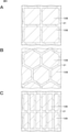
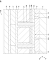
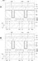
- FIG. 1 is a cross-sectional view showing a schematic configuration of an embodiment of a display device according to a first embodiment.
- FIG. 2A is a cross-sectional view showing a state of the cross section taken along line AA of FIG.
- FIG. 2B is a cross-sectional view showing a state of the cross section taken along the line BB of FIG.
- FIG. 2C is a cross-sectional view showing a state of the cross section taken along the line CC of FIG.
- FIG. 2D is a cross-sectional view showing a state of the cross section taken along the line DD of FIG.
- FIG. 2E is a cross-sectional view showing a state of the cross section taken along line EE of FIG.
- FIG. 2A is a cross-sectional view showing a state of the cross section taken along line AA of FIG.
- FIG. 2B is a cross-sectional view showing a state of the cross section taken along the line BB of FIG.
- FIG. 2C is a
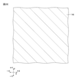
- FIG. 3A is a cross-sectional view corresponding to the state of the AA line cross section of FIG. 1 in one of the modified examples of the display device according to the first embodiment.
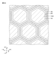
- FIG. 3B is a cross-sectional view corresponding to the state of the BB line cross section of FIG. 1 in one of the modified examples of the display device according to the first embodiment.
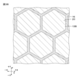
- FIG. 3C is a cross-sectional view corresponding to the state of the CC line cross section of FIG. 1 in one of the modified examples of the display device according to the first embodiment.
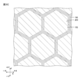
- FIG. 3D is a cross-sectional view corresponding to the state of the DD line cross section of FIG.
- FIG. 3E is a cross-sectional view corresponding to the state of the EE line cross section of FIG.
- FIG. 4A is a cross-sectional view showing a schematic configuration of an embodiment of the display device according to the second embodiment.
- FIG. 4B is a cross-sectional view showing a state of the IVB-IVB line cross section of FIG. 4A.
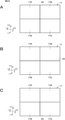
- FIG. 5A is a diagram showing a state of the VV line cross section of FIG. 4A and for explaining an embodiment of the layout of sub-pixels.
- 5B and 5C are diagrams for explaining other layout examples of sub-pixels.
- FIG. 6A is a cross-sectional view showing a schematic configuration of a modified example of the display device according to the second embodiment.
- FIG. 6B is a cross-sectional view showing a schematic configuration of a modified example of the display device according to the second embodiment.
- FIG. 7 is a cross-sectional view showing a schematic configuration of a modified example of the display device according to the second embodiment.
- 8A and 8B are plan views for explaining a modification of the display device according to the second embodiment.
- 9A, 9B, 9C, and 9D are diagrams for explaining the manufacturing method of the display device according to the second embodiment.
- 10A, 10B, 10C, and 10D are diagrams for explaining a method of manufacturing a display device according to a second embodiment.
- FIG. 11 is a cross-sectional view showing a schematic configuration of an embodiment of the display device according to the third embodiment.
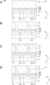
- FIGS. 12A, 12B, 12C, and 12D are diagrams for explaining a method of manufacturing a display device according to a third embodiment.
- 13A and 13B are cross-sectional views showing a schematic configuration of a modified example of the display device according to the third embodiment.
- 14A and 14B are cross-sectional views showing a schematic configuration of a modified example of the display device according to the third embodiment.
- 15A, 15B, 15C, and 15D are diagrams for explaining a manufacturing method of a modified example of the display device according to the third embodiment.
- 16A and 16B are cross-sectional views showing a schematic configuration of a modified example of the display device according to the third embodiment.
- FIG. 17A is a cross-sectional view showing a schematic configuration of an embodiment of the display device according to the fourth embodiment.
- FIG. 17B is a plan view showing a schematic configuration of an embodiment of the display device according to the fourth embodiment.
- 18A and 18B are cross-sectional views showing a schematic configuration of an embodiment of a display device according to a fourth embodiment.
- 19A and 19B are cross-sectional views showing a schematic configuration of a modified example of the display device according to the fourth embodiment.
- FIG. 20 is a cross-sectional view showing a schematic configuration of a modified example of the display device according to the fourth embodiment.
- 21A and 21B are cross-sectional views showing a schematic configuration of a modified example of the display device according to the fourth embodiment.
- 22A, 22B, and 22C are diagrams for explaining a modification of the display device according to the fourth embodiment.
- 23A, 23B, and 23C are diagrams for explaining a method of manufacturing a display device according to a fourth embodiment.
- 24A and 24B are diagrams for explaining the manufacturing method of the display device according to the fourth embodiment.
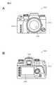
- 25A and 25B are diagrams for explaining an embodiment of an electronic device using a display device.
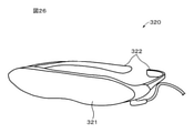
- FIG. 26 is a diagram for explaining an embodiment of an electronic device using a display device.
- FIG. 27 is a diagram for explaining an embodiment of an electronic device using a display device.
- the Z-axis direction is the vertical direction (upper side is + Z direction, the lower side is -Z direction), and the X-axis direction is the front-back direction (front side is + X direction, rear side is -X direction).
- the Y-axis direction is the left-right direction (the right side is the + Y direction and the left side is the ⁇ Y direction), and the description will be made based on this.
- This also applies to FIGS. 3A to 3E and FIGS. 4 to 24.
- the relative magnitude ratio of the size and thickness of each layer shown in each figure such as FIG. 1 is described for convenience, and does not limit the actual magnitude ratio. The rules regarding these directions and the magnitude ratio are the same for each of the figures from FIGS. 3 to 24.
- the display device according to the first embodiment of the present disclosure will be described below by exemplifying a case where the display device is an organic EL (Electroluminescence) display device.
- FIG. 1 is a cross-sectional view showing a configuration example of an organic EL display device (hereinafter, simply referred to as “display device 10A”) according to the first to fourth embodiments of the present disclosure.
- the display device 10A includes a substrate 11, an insulating layer 12, a plurality of light emitting elements 13, an insulating layer 14, a protective layer 15, a protective layer 16, a color filter 17, a filled resin layer 18, and a facing substrate 19. And prepare.
- the display device 10A is a top emission type display device.
- the substrate 11 constitutes the back surface side of the display device 10A
- the facing substrate 19 constitutes the display surface side of the display device 10A.
- the facing substrate 19 side is the top side
- the substrate 11 side is the bottom side.
- the surface on the display surface side of the display device 10A is referred to as a first surface
- the surface on the back surface side of the display device 10A is referred to as a second surface.
- the surface facing the + Z direction is referred to as a first surface
- the surface facing the ⁇ Z direction is referred to as a second surface.
- the display device 10A may be a micro display.
- the display device 10A may be used in various electronic devices. Examples of the electronic device in which the display device 10A is used include a display device for VR (Virtual Reality), MR (Mixed Reality) or AR (Augmented Reality), an electronic viewfinder (EVF) or a small projector. And so on. This also applies to the display devices 10B to 10D, which will be described later.
- the substrate 11 is a so-called backplane and drives a plurality of light emitting elements 13.
- a drive circuit including a sampling transistor for controlling the drive of the plurality of light emitting elements 13 and a drive transistor, and a power supply circuit for supplying power to the plurality of light emitting elements 13 (all shown in the figure). Is provided.
- the substrate 11 may be made of, for example, glass or resin having low permeability of water and oxygen, or may be made of a semiconductor such as a transistor which can be easily formed.
- the substrate 11 may be a glass substrate, a semiconductor substrate, a resin substrate, or the like.
- the glass substrate includes, for example, high strain point glass, soda glass, borosilicate glass, forsterite, lead glass, quartz glass and the like.
- the semiconductor substrate includes, for example, amorphous silicon, polycrystalline silicon, single crystal silicon, and the like.
- the resin substrate contains, for example, at least one selected from the group consisting of polymethylmethacrylate, polyvinyl alcohol, polyvinylphenol, polyether sulfone, polyimide, polycarbonate, polyethylene terephthalate, polyethylene naphthalate and the like.
- the insulating layer 12 is provided on the first surface of the substrate 11 and covers the drive circuit, the power supply circuit, and the like.
- the insulating layer 12 includes a plurality of contact plugs 12A and a plurality of wirings (not shown).
- the contact plug 12A connects the lower electrode 13A constituting the light emitting element 13 and the drive circuit.
- a plurality of wirings are arranged adjacent to each other in the in-plane direction (XY plane direction) of the substrate 11, and each wiring is electrically connected to the lower electrode 13A and the light emitting element 13 by a contact plug 12A or the like. Ru.
- the insulating layer 12 is made of, for example, an organic material or an inorganic material.
- the organic material contains, for example, at least one of polyimide and acrylic resin.
- the inorganic material includes, for example, at least one of silicon oxide, silicon nitride, silicon nitriding and aluminum oxide.
- the plurality of light emitting elements 13 are provided on the first surface side of the substrate 11.
- the plurality of light emitting elements 13 are two-dimensionally arranged in a predetermined arrangement pattern such as a matrix.
- the light emitting element 13 is configured to be capable of emitting white light.
- the light emitting element 13 is, for example, a white OLED or a white Micro-OLED (MOLED).
- MOLED white Micro-OLED
- as the colorization method in the display device 10A a method using a light emitting element 13 and a color filter 17 is used.
- the colorization method is not limited to this, and an RGB coloring method or the like may be used.
- a monochromatic filter may be used instead of the color filter 17, a monochromatic filter may be used.
- the colorization method is the same for the display devices 10B to the display devices 10D, which will be described later.
- the light emitting element 13 includes a lower electrode 13A, an organic layer 13B, and an upper electrode 13C.
- the lower electrode 13A, the organic layer 13B, and the upper electrode 13C are laminated in this order from the substrate 11 side toward the facing substrate 19.
- the lower electrode 13A is provided on the first surface of the insulating layer 12. As shown in FIG. 2A, the lower electrode 13A is electrically separated for each sub-pixel.
- the lower electrode 13A is an anode.
- the lower electrode 13A also functions as a reflective layer, and it is preferable that the lower electrode 13A is made of a material having as high a reflectance as possible and a large work function in order to increase the luminous efficiency.
- the sub-pixel indicates the smallest display division unit composed of one kind of color obtained by further dividing the pixel that is the division unit constituting the screen. For example, one pixel is composed of a combination of adjacent red sub-pixels, green sub-pixels, and blue sub-pixels.
- the lower electrode 13A is composed of at least one of a metal layer and a metal oxide layer. More specifically, the lower electrode 13A is composed of a single-layer film of a metal layer or a metal oxide layer, or a laminated film of a metal layer and a metal oxide layer.
- the metal oxide layer may be provided on the organic layer 13B side or the metal layer may be provided on the organic layer 13B side, but it has a high work function. From the viewpoint of adjoining the layer having the above to the organic layer 13B, it is preferable that the metal oxide layer is provided on the organic layer 13B side.
- the metal layer is, for example, chromium (Cr), gold (Au), platinum (Pt), nickel (Ni), copper (Cu), molybdenum (Mo), titanium (Ti), tantalum (Ta), aluminum (Al). , Magnesium (Mg), Tantalum (Fe), Tungsten (W) and Silver (Ag).
- the metal layer may contain at least one of the above metal elements as a constituent element of the alloy.
- alloys include aluminum alloys and silver alloys.
- Specific examples of the aluminum alloy include, for example, AlNd or AlCu.
- the metal oxide layer contains, for example, at least one of a mixture of indium oxide and tin oxide (ITO), a mixture of indium oxide and zinc oxide (IZO), and titanium oxide (TIO).
- ITO indium oxide and tin oxide
- IZO indium oxide and zinc oxide
- TIO titanium oxide
- the upper electrode 13C is provided so as to face the lower electrode 13A.
- the upper electrode 13C is formed directly above each organic layer 13B described later, and the adjacent upper electrodes 13C are formed in a state of being spatially separated for each sub-pixel, and are formed at electrode connection portions (not shown). It is electrically connected.
- the electrode connection portion may be integrated with or separate from the upper electrode 13C.
- the upper electrode 13C is a cathode.
- the upper electrode 13C is a transparent electrode having transparency to the light generated in the organic layer 13B. Here, it is assumed that the transparent electrode also includes a translucent reflective layer. It is preferable that the upper electrode 13C is made of a material having as high a transparency as possible and a small work function in order to improve the utilization efficiency of the light generated by the light emitting element 13.
- the upper electrode 13C is composed of at least one of a metal layer and a metal oxide layer. More specifically, the upper electrode 13C is composed of a single-layer film of a metal layer or a metal oxide layer, or a laminated film of a metal layer and a metal oxide layer.
- the metal layer may be provided on the organic layer 13B side or the metal oxide layer may be provided on the organic layer 13B side, but it has a low work function. From the viewpoint of making the layer adjacent to the organic layer 13B, it is preferable that the metal layer is provided on the organic layer 13B side.
- the metal layer contains, for example, at least one metal element selected from the group consisting of magnesium (Mg), aluminum (Al), silver (Ag), calcium (Ca) and sodium (Na).
- the metal layer may contain at least one of the above metal elements as a constituent element of the alloy. Specific examples of the alloy include MgAg alloy, MgAl alloy, AlLi alloy and the like.
- the metal oxide contains, for example, at least one of a mixture of indium oxide and tin oxide (ITO), a mixture of indium oxide and zinc oxide (IZO) and zinc oxide (ZnO).
- Organic layer 13B The organic layer 13B is provided between the lower electrode 13A and the upper electrode 13C.
- the organic layer 13B is patterned according to the arrangement of the sub-pixels. As shown in FIG. 2B, the organic layer 13B is formed in a state of being separated for each sub-pixel.
- the organic layer 13B is configured to be capable of emitting white light.
- the organic layer 13B has a structure in which a hole injection layer, a hole transport layer, a light emitting layer, and an electron transport layer are laminated in this order from the lower electrode 13A toward the upper electrode 13C.
- the structure of the organic layer 13B is not limited to this, and layers other than the light emitting layer are provided as needed.
- the hole injection layer is a buffer layer for increasing the hole injection efficiency into the light emitting layer and for suppressing leakage.
- the hole transport layer is for increasing the hole transport efficiency to the light emitting layer. In the light emitting layer, when an electric field is applied, recombination of electrons and holes occurs, and light is generated.
- the light emitting layer is an organic light emitting layer containing an organic light emitting material.
- the electron transport layer is for increasing the electron transport efficiency to the light emitting layer.
- An electron injection layer may be provided between the electron transport layer and the upper electrode 13C. This electron injection layer is for increasing the electron injection efficiency.
- the insulating layer 14 is provided on the first surface of the insulating layer 12.
- the insulating layer 14 electrically separates each lower electrode 13A for each light emitting element 13 (that is, for each sub-pixel).
- the insulating layer 14 has a plurality of openings 14A, and the first surface (the surface facing the upper electrode 13C) of the separated lower electrode 13A is exposed from the openings 14A.
- the insulating layer 14 may cover the separated lower electrode 13A from the peripheral edge portion to the side surface (end surface) of the first surface.
- the peripheral edge portion of the first surface means a region having a predetermined width from the peripheral edge of the first surface toward the inside.
- the protective layer 15 is an upper surface protective layer that protects the main surface (+ Z side surface) on the upper surface side of the light emitting element 13.
- the protective layer 15 is provided on the first surface of the upper electrode 13C, and covers the light emitting element 13 by covering the upper electrode 13C.
- the protective layer 15 suppresses contact between the light emitting element 13 from the upper surface side of the light emitting element 13 and the outside air, and suppresses the infiltration of moisture from the external environment into the light emitting element 13.
- the protective layer 15 may have a function of suppressing oxidation of the metal layer.
- the protective layer 15 is made of, for example, an inorganic material.
- the inorganic material constituting the protective layer 15 a material having low hygroscopicity is preferable.
- the inorganic material constituting the protective layer 15 is selected from the group consisting of silicon oxide (SiO), silicon nitride (SiN), silicon oxide nitride (SiNO), titanium oxide (TIO) and aluminum oxide (AlO). It is preferable to contain at least one of these.
- the protective layer 15 may have a single-layer structure, but may have a multi-layer structure when the thickness is increased. This is to relieve the internal stress in the protective layer 15.
- the protective layer 16 has a second protective portion 16B composed of a first protective portion 16A and a portion excluding the first protective portion 16A located directly above the protective layer 15, and the first protective portion 16A and the second protective layer 16A.
- the protective portion 16B is made of the same material and is continuously and integrally formed.
- the first protective portion covers the surface of the protective layer 15 which is the upper surface protective layer, brings about smoothing of the surface (the surface on the + Z side) together with the second protective portion 16B, and suppresses deterioration of the light emitting element 13.
- the second protective portion 16B is formed between the adjacent first protective portions 16A, and is formed so as to enter between the adjacent protective layer 15 and the adjacent light emitting elements 13.
- the second protective portion 16B also penetrates into the insulating layer 12.
- the second protective portion 16B is an inter-element separation wall that covers the side end surface 130 of the light emitting element 13.
- the element-to-element separation wall is a wall extending in a direction different from the direction of riding on the first surface of any of the layers (lower electrode 13A, organic layer 13B, upper electrode 13C) of the light emitting element 13. It is a structural part.
- the second protective portion 16B can suppress deterioration of the light emitting element 13 due to the outside air by covering the side end surface 130 of the light emitting element 13.
- the second protective portion 16B is directed from the light emitting element 13 toward the protective layer 15 (+ Z) along the thickness direction (Z-axis direction) of the light emitting element 13 with reference to the position facing the side end surface 130 of the light emitting element 13. Extends in the direction). Then, in the example of FIG. 1, the upper end (extending end) of the second protection portion 16B coincides with the upper surface side of the first protection portion 16A, and the surface of the first protection portion 16A and the upper end surface of the second protection portion 16B are aligned with each other. It is flush. As shown in the example of FIG. 1, the lower end of the second protection portion 16B is located further below the lower electrode 13A of the light emitting element 13, which will be described later in the position further below the light emitting element 13. It is preferable from the viewpoint that a low refractive index portion (void portion 20 in the example of FIG. 1) can be formed.
- the material forming the protective layer 16 (the material forming the first protective portion 16A and the second protective portion 16B) has a refractive index in the state of the protective layer 16 higher than that of the protective layer 15 forming the upper surface protective layer. It is preferable that the value of the refractive index is low. Further, since the refractive index of the protective layer 16 is smaller than the refractive index of the protective layer 15, it is possible to more effectively prevent the light generated by the light emitting element from leaking to the adjacent sub-pixel side. Therefore, when the material forming the protective layer 16 satisfies the refractive index as described above, it is possible to more effectively prevent the light generated by the light emitting element from leaking to the adjacent sub-pixel side.
- the material forming the protective layer 16 is preferably made of a material having a step coverage value of less than 1. Further, the material forming the protective layer 16 is preferably made of a material having a lower moisture permeability than the protective layer 15 serving as the upper surface protective layer. By forming the protective layer 16 with such a material, the void portion 20 can be formed more efficiently.
- Examples of the material for forming the protective layer 16 include SiN, Al 2 O 3 , TiO 2 and the like formed by a method such as a PECVD (plasma-enhanced chemical vapor deposition) method or a sputtering method.
- PECVD plasma-enhanced chemical vapor deposition
- a low refractive index portion having a lower refractive index than that of the second protective portion 16B is formed inside the second protective portion 16B forming the separation wall between the elements.
- the low refractive index portion is formed in a shape extending in the thickness direction (Z-axis direction) of the light emitting element.
- the low refractive index portion is a portion having a refractive index lower than the refractive index of the second protective portion 16B.
- the low refractive index portion include a gas space portion filled with a specific gas such as nitrogen, a liquid portion filled with a specific liquid, and the like. As the gas space portion, an air-filled void portion can be exemplified.
- the refractive index of the low refractive index portion and the refractive index of the second protected portion are the refractive index of the low refractive index portion and the refractive index of the second protected portion in the display device.
- the refractive index of the void portion 20 is smaller than that of the second protective portion 16B, total reflection of light may occur at the interface between the portion made of the material forming the protective layer 16 and the void portion 20. It will be easy.
- the void portion 20 is formed as a low refractive index portion.
- the description will be continued by taking the case where the void portion 20 is formed as a low refractive index portion as an example.
- the length and position of the gap 20 in the vertical direction are not limited.
- the gap 20 may be formed at at least one of the lower electrode 13A, the organic layer 13B, the upper electrode 13C, and the protective layer 15, and has a length corresponding to the position. good.
- the gap portion 20 exists at any of the positions of the lower electrode 13A, the organic layer 13B, the upper electrode 13C, and the protective layer 15 in the vertical direction (Z-axis direction). Further, it exists up to a height position near the center of the first protection portion 16A in the Z-axis direction.
- the example of the void portion 20 is not limited to this, and may be formed, for example, at the position of the organic layer 13B with a length corresponding to the thickness of the organic layer 13B.
- the upper end of the gap portion 20 is above the interface between the light emitting element 13 and the protective layer 15 (+ Z direction side). It is preferable to have.
- the gap portion 20 is formed from the position near the first surface of the substrate 11 to the position near the second surface of the color filter 17, so that the light generated in the organic layer 13B is surely leaked to the adjacent sub-pixel side. It is even more preferable from the viewpoint that it can be made difficult.
- the lower end of the gap 20 may be located below the lower electrode 13A as well as the lower end of the second protective portion 16B. It is more preferable that the position in the insulating layer 12 is lower than the position between adjacent wirings or the position between adjacent wirings. In this case, since the gap portion 20 is arranged between the wirings adjacent to each other in the XY plane direction, the capacitance (parasitic capacitance) of the capacitor formed by the adjacent wirings is compared with the case where the gap portion 20 does not exist. ) Can be reduced.
- the cross-sectional shape of the gap portion 20 has a bottom surface portion 20A, a bottom surface portion 20A thereof, and a side wall portion 20B.
- the gap portion 20 preferably has a taper angle (angle ⁇ in FIG. 1) formed by the bottom surface portion 20A and the side wall portion 20B of 90 ° or less.
- the taper angle ⁇ is formed in a forward taper shape of 30 ° or less.
- this does not prohibit the shape of the gap 20 from being reverse-tapered, and the shape of the gap 20 may be reverse-tapered.
- the cross-sectional shape of the gap portion 20 is a cross-sectional trapezoidal shape in the example of FIG. 1, but the cross-sectional shape is not limited to this, and may be a triangle, a polygon of a quadrangle or more, or a curved surface portion.
- the void portion 20 is formed only between the adjacent protective layers 15. You may. In that case, the second protective portion 16B in the protective layer 16 may be formed only in the portion between the adjacent protective layers 15, or both between the adjacent protective layers 15 and between the adjacent light emitting elements 13. It may be formed over a portion of. When the second protective portion 16B is formed only in the portion between the adjacent protective layers 15, the organic layer 13B and the upper electrode 13C are not separated for each sub-pixel but are shared among the sub-pixels.
- the color filter 17 is provided on the protective layer 16.
- the color filter 17 is, for example, an on-chip color filter (OCCF).
- the color filter 17 includes, for example, a red filter, a green filter, and a blue filter.
- the red filter, the green filter, and the blue filter are provided facing the light emitting element 13 for the red sub-pixel, the light emitting element 13 for the green sub pixel, and the light emitting element 13 for the blue sub pixel, respectively.
- the white light emitted from each of the light emitting elements 13 in the red sub-pixel, the green sub-pixel, and the blue sub-pixel passes through the above-mentioned red filter, green filter, and blue filter, respectively, so that the red light and the green light are emitted.
- Blue light is emitted from the display surface, respectively.
- a light-shielding layer (not shown) may be provided between the color filters of each color, that is, between the sub-pixels.
- the color filter 17 is not limited to the on-chip color filter, and may be provided on one main surface of the facing substrate 19.
- the filling resin layer 18 is provided between the color filter 17 and the facing substrate 19.
- the filled resin layer 18 has a function as an adhesive layer for adhering the color filter 17 and the facing substrate 19.
- the packed resin layer 18 contains, for example, at least one of a thermosetting resin and an ultraviolet curable resin.
- the facing substrate 19 is provided so as to face the substrate 11. More specifically, the facing substrate 19 is provided so that the second surface of the facing substrate 19 and the first surface of the substrate 11 face each other.
- the facing substrate 19 and the filled resin layer 18 seal the light emitting element 13, the color filter 17, and the like.
- the facing substrate 19 is made of a material such as glass that is transparent to each color light emitted from the color filter 17.
- a drive circuit, a power supply circuit, and the like are formed on the first surface of the substrate 11 by using, for example, a thin film forming technique, a photolithography technique, and an etching technique.
- an insulating layer 12 is formed on the first surface of the substrate 11 so as to cover the drive circuit and the power supply circuit, and then a plurality of contact plugs 12A are formed on the insulating layer 12.
- a laminated film of a metal layer and a metal oxide layer is formed on the first surface of the substrate 11 by a sputtering method, and then the laminated film is patterned by using, for example, a photolithography technique and an etching technique.
- the lower electrode 13A separated for each light emitting element 13 (that is, for each sub pixel) is formed.
- an insulating layer 14 is formed on the first surface of the insulating layer 12 so as to cover the plurality of lower electrodes 13A, and then the insulating layer 14 is patterned using a photolithography technique and an etching technique. do. As a result, a plurality of openings 14A are formed in the insulating layer 14. If the lower electrode 13A is not easily damaged by the groove forming process (groove processing) described later, the insulating layer 14 may be omitted.
- the hole injection layer, the hole transport layer, the light emitting layer, and the electron transport layer are laminated on the first surface of the first surface of the lower electrode 13A in this order to form an organic layer.
- the upper electrode 13C is formed on the first surface of the organic layer 13B by, for example, a vapor deposition method or a sputtering method. As a result, a plurality of light emitting elements 13 are formed on the first surface of the insulating layer 12.
- the protective layer 15 is formed on the first surface of the upper electrode 13C by, for example, a CVD method or a vapor deposition method. Then, the light emitting element and the protective layer are grooved along the layout of the sub-pixels by, for example, photolithography technology and etching technology. In the display device of FIG. 1, a groove is formed to the inside of the insulating layer 12. Further, the protective layer 16 is formed on the surface of the protective layer 15 and inside the groove by a method such as a PECVD method or a sputtering method.
- the gap portion 20 is formed in the second protection portion 16B. Will be done.
- the color filter 17 is formed on the first surface of the protective layer 15 by, for example, photolithography.
- the color filter 17 is covered with the filled resin layer 18, and then the facing substrate 19 is placed on the filled resin layer 18.
- the display device 10A is sealed.
- the display device 10A shown in FIG. 1 is obtained.
- a second protective portion 16B serving as an inter-element separation wall is formed between adjacent sub-pixels so as to face the side end surface 130 of the light emitting element 13.
- a low refractive index portion is formed inside the second protective portion 16B.
- the low refractive index portion is the gap portion 20, and the gap portion 20 is located below the lower electrode 13A, and the wiring is adjacent to the insulating layer 12.
- the capacitance between wirings can be reduced.
- the shape of the sub-pixel is rectangular, but the shape is not limited to this, and may be formed into a hexagonal shape as shown in FIGS. 3A to 3E. Further, the arrangement of the sub-pixels is not limited to the matrix shape, and may be a honeycomb shape as shown in FIGS. 3A to 3E. Even in such a case, it becomes possible to suppress the leakage of light to the adjacent sub-pixels in the same manner as described in the above-mentioned action and effect.
- FIG. 4A is a cross-sectional view showing a configuration example of an organic EL display device (display device 10B) according to an example of the second embodiment.
- FIG. 4B is a diagram illustrating a state of the IVB-IVB line cross section of FIG. 4A.
- the display device 10B is a top emission type display device.
- the display device 10B includes a substrate 11, an insulating layer 12, a plurality of light emitting elements 13, a protective layer 15 as an upper surface protective layer, a separation film 21 as a separation wall between elements, a color filter 17, and a filled resin layer. 18 and a facing substrate 19 are provided.
- the substrate 11, the insulating layer 12, the protective layer 15, the color filter 17, the filled resin layer 18, and the facing substrate 19 are the same as those in the first embodiment.
- the display device 10B of the second embodiment it is not necessary to provide the structure of the insulating layer 14 in the first embodiment.
- the plurality of light emitting elements 13 are provided on the first surface of the substrate 11, include a lower electrode 13A and an organic layer 13B, and an upper electrode laminated on the organic layer 13B.
- First upper electrode 13D is provided.
- the lower electrode 13A and the organic layer 13B are the same as those in the first embodiment, and are separated from each other for each sub-pixel.
- the upper electrode laminated on the organic layer 13B is the first upper electrode 13D, which is separated from each other for each sub-pixel.
- the first upper electrode 13D faces the lower electrode 13A, and the first upper electrode 13D faces the protective layer 15.
- the second upper electrode 13E electrically connects the adjacent first upper electrodes 13D to each other.
- the second upper electrode 13E extends along the surface of the separation membrane 21 to the extending end 21A of the separation membrane 21 with the facing position of the first upper electrode 13D and the separation membrane 21 as the base end.
- the position of the upper end portion of the second upper electrode 13E and the position of the surface of the protective layer 15 are aligned with the second upper electrode 13E formed on the surface of the separation film 21.
- the second upper electrode 13E is formed so as to cover the entire portion of the separation membrane 21 extending upward from the first upper electrode 13D.
- the second upper electrode 13E is further made of a reflective material as described later, the light traveling diagonally among the light generated by the light emitting element 13 is effectively reflected by the second upper electrode 13E. It is possible to increase the efficiency of light utilization.
- the second upper electrodes 13E are formed in a grid pattern according to the layout of the sub-pixels, and the individual first upper electrodes 13D are formed in a rectangular shape and arranged in a matrix.
- the first upper electrode 13D and the second upper electrode 13E are cathodes.
- the first upper electrode 13D is a transparent electrode having transparency to the light generated in the organic layer 13B.
- the transparent electrode also includes a translucent reflective layer.
- the first upper electrode 13D is made of a material having as high a transparency as possible and a small work function in order to increase the luminous efficiency.
- the reflectance of the second upper electrode 13E is larger than the reflectance of the first upper electrode 13D.
- the reflectance of the second upper electrode 13E and the reflectance of the first upper electrode 13D are the reflectance of the second upper electrode 13E and the reflectance of the first upper electrode 13D in the state of the display device 10B.
- a reflective material can be used as the material of the second upper electrode 13E. Examples of the reflective material include silver (Ag), aluminum (Al), and tungsten (W).
- the display device 10B is formed with a separation film 21 that covers the side end surface 130 side of the light emitting element 13 as an inter-element separation wall.
- the separation film 21 is arranged between adjacent light emitting elements 13, and separates the lower electrode 13A, the organic layer 13B, and the first upper electrode 13D forming the light emitting element 13 for each sub-pixel.
- the upper end side portion of the separation film 21 extends from the light emitting element 13 toward the protective layer 15 along the thickness direction (Z-axis direction) of the light emitting element 13.
- the separation film 21 has a shape that extends from the light emitting element 13 toward the protective layer 15 (Z-axis direction) instead of the surface direction (XY plane direction) of the light emitting element 13. It becomes difficult to cover the light emitting region of the light emitting element, and a wider light emitting region can be secured.
- the separation membrane 21 is made of an insulator.
- the separation film 21 include an inorganic insulating film and an organic insulating film.
- the inorganic insulating film include SiO 2 , SiN, and SiON.
- the organic insulating film include polyimide and the like.
- the length of the separation membrane 21 in the vertical direction (Z-axis direction) is larger than the sum of the thickness of the lower electrode 13A, the thickness of the organic layer 13B, and the thickness of the first upper electrode 13D. It is preferable from the viewpoint of facilitating the formation of a portion extending above the electrode 13D.
- the lower end of the separation membrane 21 is located near the insulating layer 12 below the lower end of the lower electrode 13A, and the separation membrane 21 separates the lower electrode 13A for each sub-pixel.
- the separation membrane 21 may be located at the lower end of the lower electrode 13A.
- the separation membrane 21 may separate the lower electrode 13A for each sub-pixel.
- the upper end of the separation film 21 is located slightly below the position of the surface of the protective layer 15, and the second upper electrode 13E is formed on the surface of the separation film 21.
- the position of the extending end portion of the protective layer 15 and the position of the surface of the protective layer 15 are aligned.
- the refractive index of the separation membrane 21 is smaller than the refractive index of the second upper electrode 13E. In this case, among the light generated by the light emitting element 13, the light traveling diagonally can be totally reflected at the interface between the second upper electrode 13E and the separation film 21, and the light utilization efficiency can be improved.
- the refractive index of the separation membrane 21 and the refractive index of the second upper electrode 13E are the refractive index of the separation membrane 21 and the refractive index of the second upper electrode 13E in the state of the display device 10B.
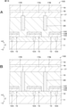
- FIGS. 9A to 9D and FIGS. 10A to 10D are diagrams for explaining the manufacturing method of the display device 10B according to the second embodiment.
- the step of forming the first laminated body in which the lower electrode 13A, the organic layer 13B, the first upper electrode 13D, and the protective layer 15 are laminated in this order on the substrate 11 on which the insulating layer 12 is formed is carried out as shown below. ..
- a drive circuit, a power supply circuit, and the like are formed on the first surface of the substrate 11 by using a thin film forming technique, a photolithography technique, and an etching technique.
- a CVD method an insulating layer 12 is formed on the first surface of the substrate 11 so as to cover the drive circuit and the power supply circuit, and then a plurality of contact plugs 12A are formed on the insulating layer 12.
- a laminated film (lower electrode) of a metal layer and a metal oxide layer is formed on the first surface of the substrate 11 by a sputtering method.
- the hole injection layer, the hole transport layer, the light emitting layer, and the electron transport layer are laminated on the first surface of the first surface of the lower electrode 13A in this order to form an organic layer.
- the first upper electrode 13D is formed on the first surface of the organic layer 13B by a vapor deposition method or a sputtering method.
- the protective layer 15 is formed on the first surface of the first upper electrode 13D by a CVD method or a vapor deposition method.
- the first laminated body 40 is formed.
- a step of forming a first groove from the protective layer 15 to a predetermined depth in the first laminated body 40 at a predetermined position according to the layout of the sub-pixels (first step). Grooving process) is performed.
- the first grooving step is a step of grooving the light emitting element 13 and the protective layer 15 along the layout of the sub-pixels by, for example, a photolithography technique and an etching technique.
- the protective layer 15, the first upper electrode 13D, the organic layer 13B, the lower electrode 13A, and the insulating layer 12 are collectively grooved to form the first groove 22.
- a step of forming the separation film 21 in the first groove 22 is carried out by, for example, a CVD (Chemical Vapor Deposition) method, a coating method, or the like.
- the material forming the separation film 21 is also laminated on the outside of the first groove 22, such as on the surface of the protective layer 15, so that the outer laminated portion of the first groove 22 is as shown in FIG. 9C. Is formed, but the outer laminated portion of the first groove 22 is removed by a CMP (chemical mechanical polishing) method, an etch back method, or the like.
- the second laminated body 41 is formed as shown in FIG. 9D.
- the CVD method for example, an inorganic insulating film such as SiO 2 , SiN, or SiON can be formed.
- an organic insulating film such as polyimide can be formed.
- a step (second groove processing step) of forming the second groove 23 from the protective layer 15 to the position of the first upper electrode 13D is carried out in a predetermined region around the separation film 21.
- the second grooving step is a step in which grooving is performed by, for example, a photolithography technique and an etching technique, similarly to the above-mentioned first groove.
- the depth of the second groove 23 is such that it reaches the first upper electrode 13D, and the first upper electrode 13D is exposed on the bottom surface of the second groove 23.
- Reference numeral 50 in FIG. 10A is a resist for forming the second groove 23.
- a step of forming the second upper electrode 13E in the second groove 23 is carried out.
- the material forming the second upper electrode is also laminated on the outside of the second groove, such as on the surface of the protective film, so that the outer laminated portion of the second groove 23 is laminated as shown in FIG. 10C.
- the outer laminated portion of the second groove is removed by a CMP method, an etchback method, or the like, as in the case of the outer laminated portion of the first groove.
- the third laminated body 42 is formed.
- the outer laminated portion of the second groove 23 is left unremoved in the case of the third modification described later in the second embodiment.
- the color filter 17 is formed on the first surface of the third laminated body 42 by, for example, photolithography.
- the color filter 17 is covered with the filled resin layer 18, and then the facing substrate 19 is placed on the filled resin layer 18.
- the display device 10B is sealed. From the above, the display device 10B is obtained.
- the lower electrode 13A, the organic layer 13B, and the first upper electrode 13D forming the light emitting element 13 by the separation film 21 are separated for each sub-pixel.
- the organic layer 13B is surrounded by the separation film 21 and separated for each sub-pixel, it is possible to suppress the leakage of light in the lateral direction to the adjacent sub-pixels.
- the separation film 21 extends in the vertical direction, an insulating film is formed so as to ride on the peripheral edge of the first electrode patterned and formed for each sub-pixel, and the separation film 21 is separated for each sub-pixel. Therefore, it becomes easier to secure a wider light emitting region of the light emitting element.
- the second upper electrode 13E has a higher reflectance than the first upper electrode 13D, so that the light generated by the light emitting element 13 is reflected by the second upper electrode 13E. This makes it possible to prevent the light generated by the light emitting element 13 from leaking to the adjacent sub-pixel side.
- the separation membrane 21 has a lower refractive index than the second upper electrode 13E, so that the light generated by the light emitting element 13 is the second upper electrode 13E and the separation membrane 21. It becomes easy to totally reflect at the interface of the above, and it becomes possible to suppress the light generated by the light emitting element 13 from leaking to the adjacent sub-pixel side (suppress the light leakage between the adjacent pixels).
- the light generated by the light emitting element 13 is suppressed from leaking to the adjacent sub-pixels, so that the color mixing can be suppressed and the viewing angle can be suppressed. Deterioration can be suppressed.
- the shape of the sub-pixels is formed in a rectangular shape as shown in FIGS. 4B and 5A, and a plurality of sub-pixels are arranged separately from each other in a matrix.
- the shape of the sub-pixels is not limited to this, and may be a hexagonal shape or a striped shape as shown in FIGS. 5B and 5C.
- the arrangement of the sub-pixels is not limited to the matrix shape, and may be a honeycomb shape as shown in FIG. 5B. Even in such a case, unintended light emission due to current leakage is suppressed, as described in the above-mentioned action and effect. In addition, it becomes possible to suppress light leakage to adjacent sub-pixels.
- Modification 2 Regarding the display device 10B according to the second embodiment, in the above description, the position of the extended end portion of the second upper electrode 13E and the surface of the protective layer 15 in a state where the second upper electrode 13E is formed on the surface of the separation film 21.
- the case where the positions are aligned is taken as an example.
- the display device 10B according to the second embodiment is not limited to this example, and the extending end portion of the second upper electrode 13E is further above (as shown in FIG. 6A) beyond the position of the surface of the protective layer 15. It may be located in the + Z direction) and enter the color filter 17, or may not reach the position of the surface of the protective layer 15 as shown in FIG. 6B.
- the second upper electrode 13E is formed along the surface of the separation film 21 so as to cover the surface of the separation film 21.
- the display device 10B according to the second embodiment is not limited to this example.
- the second upper electrode 13E is not only formed along the surface of the separation membrane 21 up to the extending end of the separation membrane 21, but also protected from the extending end of the separation membrane 21. It may extend along the surface of the layer 15.
- a portion extending along the surface of the protective layer 15 is referred to as a extending electrode portion 24.
- the extending electrode portion 24 preferably covers the entire surface of the protective layer 15.
- the second upper electrode 13E is a transparent electrode or a translucent electrode from the viewpoint of allowing the light generated from the light emitting element 13 to pass through the extending electrode portion 24 and be efficiently taken out to the outside. It is preferable that it is formed.
- the second upper electrode 13E When the second upper electrode 13E is formed of a translucent electrode, the second upper electrode 13E has an extended electrode portion, and the separation distance between the light emitting surface of the organic layer 13B and the extended electrode portion 24 By adjusting the above, it is possible to improve the light extraction effect accompanying the light resonance effect, and it is possible to obtain a display device 10B having excellent brightness.
- the second upper electrode 13E was formed so as to cover the entire surface of the portion of the separation membrane 21 extending upward from the first upper electrode 13D, but the display device 10B according to the second embodiment is this.
- the present invention is not limited to the example, and as shown in FIGS. 8A and 8B, the separation membrane 21 may be formed so as to cover a part of the portion extending upward from the first upper electrode.
- the portion of the separation membrane 21 extending upward from the first upper electrode 13D corresponding to the apex portion of the adjacent sub-pixel. It may be formed to cover.
- the portion of the separation membrane 21 in which the second upper electrode 13E extends upward from the first upper electrode 13D corresponds to the side portion of the adjacent sub-pixel. It may be formed to cover.
- the side wall protective film may be interposed between the side end surface of the organic layer 13B and the separation film 21 (third embodiment).
- FIG. 11 is a cross-sectional view showing a configuration example of an organic EL display device (display device 10C) according to an example of the third embodiment.
- the display device 10C has a side wall protective film in addition to each configuration of the display device 10B according to the second embodiment. As shown in the example of FIG. 11, the display device 10C includes a substrate 11, an insulating layer 12, a plurality of light emitting elements 13, a protective layer 15, a side wall protective film 25, and a separation film 21 as an inter-element separation wall. A color filter 17, a filling resin layer 18, and a facing substrate 19 are provided.
- the side wall protective film 25 is interposed between the side end surface of the organic layer 13B and the separation film 21. As shown in FIG. 11, it is preferable that the side wall protective film 25 covers the entire side end surface of the organic layer 13B while being in contact with the side end surface of the organic layer 13B.
- the side wall protective film 25 is an insulating film, and is a processed by-product film containing a by-product (depot) generated by etching processing.
- the side wall protective film 25 assists in forming the separation film 21 while restricting the exposure of the organic layer 13B to the external environment.
- the etching process referred to here refers to the process by the etching method in the first groove processing step shown in the description of the manufacturing method of the display device 10C according to the third embodiment described later.
- the etching process either a dry etching method or a wet etching method can be carried out, but from the viewpoint of more reliably realizing the depot, the etching process is preferably a dry etching method.
- the side wall protective film 25 shown in FIG. 11 is formed so that its thickness is uniform, but this is not limited to the case where the thickness of the side wall protective film 25 is uniform.
- the side wall protective film 25 may be formed so that the thickness gradually decreases as the distance from the vicinity of the auxiliary layer 26 described later increases.
- the auxiliary layer 26 is interposed between the lower electrode 13A and the substrate 11 or between the first upper electrode 13D and the protective layer 15. be.
- the auxiliary layer 26 is formed between the lower electrode 13A and the substrate 11 under the lower electrode 13A.
- the contact plug 12A is also formed in the auxiliary layer 26, and the electrical connection with the drive circuit on the substrate 11 side is secured.
- the auxiliary layer 26 is a depot generation film made of a material that easily causes depot during etching.
- a material for the auxiliary layer 26, which easily forms a by-product (depot) during etching for example, a difficult-to-etch material having a lower volatility of a metal halogen compound and a stronger metal-oxygen bond is used. It is preferably used.
- the material of the auxiliary layer 26 it is preferable to use a transition metal oxide such as Al2O3 . However, this does not mean that the material of the auxiliary layer 26 is limited to the transition metal oxide.
- the material of the auxiliary layer 26 may be any material that can form an insulating film on the side end surface of the organic layer 13B.
- the side wall protective film 25 is formed so as to extend from the auxiliary layer 26 along the side end surface 130 of the light emitting element 13 with the auxiliary layer 26 as the base end.
- the side wall protective film 25 contains at least one element forming the auxiliary layer 26.
- the film composition of the side wall protective film 25 is different from the film composition of the separation film 21.
- the auxiliary layer 26, the lower electrode 13A, the organic layer 13B, the first upper electrode 13D, and the protective layer 15 are laminated in this order on the substrate 11 on which the insulating layer 12 is formed, and the first laminated body 43 is formed.
- a resist 51 is provided in the first laminated body 43, and a first groove 27 is formed in the protective layer 15 at a predetermined position as shown in FIG. 12C.
- each layer forming the light emitting element 13 is etched (groove processing step).
- the first groove 27 is further formed downward, and the auxiliary layer 26 is also etched together with the lower electrode 13A, the organic layer 13B, and the first upper electrode 13D forming the light emitting element 13.
- the auxiliary layer 26 is also etched together with the lower electrode 13A, the organic layer 13B, and the first upper electrode 13D forming the light emitting element 13.
- a depot is generated and adheres to the side end faces of the lower electrode 13A, the organic layer 13B, and the first upper electrode 13D to form the side wall protective film 25 (FIG. 12D). In this way, a state in which the side wall protective film 25 is formed along the inner wall of the first groove 27 is formed.
- the same step as the manufacturing method of the display device according to the second embodiment is carried out. That is, a step of forming the separation film 21 in the first groove 27 and a step of forming a second groove 23 from the protective layer 15 to the position of the first upper electrode 13D in a predetermined region around the separation film 21.
- the step of forming the second upper electrode 13E in the second groove 23 is carried out. After the second upper electrode 13E is formed, the color filter 17, the filled resin layer 18, and the facing substrate 19 are laminated. As a result, the display device 10C according to the third embodiment is obtained.
- the side wall protective film is formed so as to cover the side end faces of the organic layer.
- the side wall protective film is a depot generation film formed at the time of etching processing in the step before forming the separation film (first groove processing step). Therefore, even when the separation membrane is formed after the first grooving step, the side end faces of the organic layer are suppressed from being exposed to an external environment (under a low vacuum environment), and the organic layer is prevented from being exposed. The characteristics of can be improved.
- FIGS. 12A to 12D a display device is shown when the auxiliary layer 26 does not remain inside the first groove 27 during the grooving process. That is, in the display device 10C shown in FIG. 11 obtained in this case, the side wall protective film 25 is not provided on the lower end surface of the separation film 21.
- the display device according to the third embodiment is not limited to this, and as shown in FIG. 14A, the side wall protective film 25 may be provided on the lower end surface of the separation film 21. This can be realized by leaving the auxiliary layer 26 in the first groove 27 during the first groove processing step.
- auxiliary layer 26 is located in a predetermined region between the sub-pixels. It may be formed in a limited manner.
- the auxiliary layer 26 is formed at a position corresponding to the side end surface 130 of the light emitting element 13 when the thickness direction of the light emitting element 13 is the line-of-sight direction, and at a position below the lower electrode 13A.
- the side wall protective film 25 extends upward from the auxiliary layer 26.
- the auxiliary layer 26 may be interposed between the first upper electrode 13D and the protective layer 15.
- Such a display device 10C can be manufactured, for example, as follows.
- the lower electrode 13A, the organic layer 13B, and the first upper electrode 13D are formed on the surface of the substrate 11 in the same manner as in the manufacturing method of the display device according to the second embodiment.
- the auxiliary layer 26 is formed on the first upper electrode 13D (FIG. 15A).
- a resist 52 is provided on the auxiliary layer 26 (FIG. 15B), and a first groove 27 is formed in the auxiliary layer 26 at a predetermined position corresponding to a pixel layout such as a sub pixel by using a photolithography technique and an etching technique. do.
- a depot is attached to the inner wall portion of the first groove 27 (FIG. 15C).
- a groove processing step is carried out by a photolithography technique, an etching technique, or the like.
- the lower electrode 13A, the organic layer 13B, and the first upper electrode 13D forming the light emitting element 13 are etched, and the first groove 27 is further formed downward.
- the depot derived from the auxiliary layer 26 also adheres to the side end surfaces of the lower electrode 13A, the organic layer 13B, and the first upper electrode 13D, and the side wall protective film 25 is formed. It is formed (Fig. 15D). In this way, a state in which the side wall protective film 25 is formed in the first groove 27 is formed.
- the separation film 21 is formed inside the first groove 27 by a method such as a CVD method or a coating method.
- a method such as a CVD method or a coating method.
- the material laminated on the outside of the first groove 27 is removed by the CMP method or the etchback method.
- a protective layer 15 is formed on the surface side of the auxiliary layer 26.
- a step of forming a groove in the protective layer 15 is performed at a position corresponding to the first groove 27 with respect to the protective layer 15.
- the separation film 21 is formed inside the groove formed in the protective layer 15 by a method such as a CVD method or a coating method. As a result, the separation film 21 is formed from the surface position of the protective layer 15 to the position of the lower electrode 13A along the thickness direction of the light emitting element 13. From this point onward, a display device can be obtained in the same manner as in the method for manufacturing a display device according to the second embodiment described above.
- a step of forming the second groove 23 from the protective layer 15 to the position of the first upper electrode 13D in a predetermined region around the separation membrane 21, and a step of forming the second upper electrode 13E in the second groove 23. Is carried out. After the second upper electrode 13E is formed, the color filter 17, the filled resin layer 18, and the facing substrate 19 are laminated. As a result, the display device 10C is obtained.
- the side wall protective film 25 shown in FIG. 14B is formed so that its thickness is uniform, but this is not limited to the case where the thickness of the side wall protective film 25 is uniform.
- the side wall protective film 25 may be formed so that the thickness gradually decreases as the distance from the vicinity of the auxiliary layer 26 described later increases.
- the display device according to the fourth embodiment of the present disclosure will be described below by taking the case where the display device is an organic EL display device as in the first embodiment as an example.
- FIGS. 17A and 17B are cross-sectional views showing a configuration example of an organic EL display device (display device 10D) according to an example of the fourth embodiment.
- the display device 10D is a top emission type display device.
- the display device 10D includes a substrate 11, an insulating layer 12, a plurality of light emitting elements 13, a protective layer 15, a light absorbing layer 28, and a color filter 17.
- the description of the insulating layer corresponding to the insulating layer 14 in the first embodiment is omitted. This also applies to FIGS.
- the insulating layer corresponding to the insulating layer 14 is the same as that of the insulating layer 14 in the first embodiment. It may be omitted.
- the substrate 11, the insulating layer 12, the protective layer 15 as the upper surface protective layer, and the color filter 17 are the same as those in the first embodiment.
- a plurality of color filters 17 are provided according to the type of sub-pixels.
- the display device 10D includes a red filter 17R, a green filter 17G, and a blue filter 17B as the color filter 17. The case will be described.
- the red filter 17R, the green filter 17G, and the blue filter 17B are provided facing the light emitting element 13 for the red sub-pixel, the light emitting element 13 for the green sub pixel, and the light emitting element 13 for the blue sub pixel, respectively, and display.
- the gaps or boundaries of the adjacent color filters 17 are located in the gaps of the adjacent light emitting elements 13.
- the light absorption layer 28 is formed at a position of a gap or a boundary between adjacent color filters 17 in a plan view of the display device 10D (in a plan view of the light emitting element 13).
- FIG. 17B is a diagram illustrating the positional relationship between the color filter 17 and the light absorption layer 28.
- the light absorption layer 28 is formed at a position between the color filter 17 and the lower electrode 13A in the thickness direction of the light emitting element 13.
- the light absorption layer 28 has a shape extending from the color filter 17 toward the substrate 11 (downward), and has a width W (width W) in a direction along the in-plane direction (XY plane direction) of the color filter 17. ),
- the length H in the direction along the depth direction of the color filter 17 is formed to be longer (H> W).
- the lower end of the light absorption layer 28 is located above the light emitting element 13. In this case, it is possible to prevent the incident light L of the external light incident obliquely from propagating across the sub-pixels.
- a black color filter, a complementary color filter, a non-adjacent color filter, an absorption film, or the like can be used.
- a black color filter a color filter using carbon, titanium black or the like as a coloring material can be exemplified.
- the complementary color filter a color filter using a complementary color material for the color of the color filter which is the base end of the light absorption layer 28 can be exemplified.
- the non-adjacent color filter can exemplify a color filter corresponding to a color type other than that color type when the color types of the adjacent color filters serving as the base end of the light absorption layer 28 are different.
- the color filter 17 includes a red filter 17R, a green filter 17G, and a blue filter 17B
- the light absorption layer 28 is located at the boundary between the green filter 17G and the red filter 17R.
- an organic material film, an inorganic material film, or the like can be exemplified.
- a resin film containing a black pigment for example, carbon black
- a metal oxide film, a single metal film, or the like is preferable, and a metal oxide film is particularly preferable from the viewpoint of excellent light absorption.
- [4-2 Manufacturing method of display device] The method for manufacturing the display device according to the fourth embodiment can be carried out, for example, as described below. A case where the display devices shown in FIGS. 17A and 17B are manufactured will be described as an example.
- the insulating layer 12, the lower electrode 13A, the organic layer 13B, and the upper electrode 13C are placed on the first surface of the substrate 11 on which the insulating layer 12 is formed.
- the protective layer 15 is laminated to form the first laminated body 44 (FIG. 23A).
- the insulating layer is also formed.
- the first laminated body 44 is grooved along the layout of the sub-pixels by, for example, a photolithography technique and an etching technique to form a groove 29 having a predetermined depth (FIG. 23B). ..
- the groove 29 is formed at a depth within the protective layer 15 to a predetermined position.
- a step of forming the light absorption layer 28 in the groove 29 is carried out by a method such as a CVD method or a coating method.
- the color filter 17 is formed on the surface side of the protective layer 15 by, for example, photolithography (FIG. 24A). Therefore, the color filter 17 is an on-chip type.
- a lens 30 may be formed on the 17th surface of the color filter (FIG. 24B). The lens 30 can be formed by applying an on-chip microlens (OCL) forming method using a melting method, an etchback method, or the like. As a result, the display device 10D shown in FIGS. 17A and 17B can be obtained.
- OCL on-chip microlens
- external light may be incident at an angle, reflected by the lower electrode to form reflected light, and the reflected light may be output to the outside.
- the incident light or reflected light of the obliquely incident external light propagates across the sub-pixels, and the sub-pixels that pass at the time of incident and the sub-pixels that pass after being reflected by the electrode layer are different, the incident light or The sub-pixels through which the reflected light passes may cause color mixing or mixing of the light, resulting in a decrease in the contrast of the display device.
- the display device 10D according to the fourth embodiment since the light absorption layer 28 extends from the color filter 17 toward the protective layer 15, the light is obliquely incident.
- the incident light L of the external light is absorbed by the light absorption layer 28, and it becomes possible to suppress the leakage of the light to the adjacent sub-pixels. Therefore, it is less likely that the incident light or the reflected light of the external light incident obliquely propagates across the sub-pixels, and a display device having excellent contrast can be obtained.
- the light U from the light emitting element is also suppressed from leaking to the adjacent sub-pixels as in the incident light L of the external light incidently incidently. Therefore, it is possible to suppress the color mixing and mixing of light between the sub-pixels.
- the vertical length of the light absorption layer 28 is not limited to the example of FIG. 17A. As shown in FIG. 18B, the light absorption layer 28 may extend from the position of the boundary of the adjacent color filters 17 to the space between the adjacent light emitting elements 13. Further, in that case, the tip of the light absorption layer 28 may penetrate to the insulating layer 12. In the example of FIG. 18B, the light absorption layer 28 separates the adjacent light emitting elements 13, so that the light absorption layer 28 can function as an inter-element separation wall.
- the light absorption layer 28 is not limited to the example of FIG. 17A, and may be formed so that the upper end of the light absorption layer 28 is at a position inside the color filter 17, for example, as shown in FIG. 18A. .. In this case, since the light absorption layer 28 spreads to the inside of the color filter 17, the light from the light emitting element 13 is suppressed from leaking to the adjacent sub-pixels at the position of the color filter 17, and the color of the light is mixed. ⁇ Mixing can be suppressed.
- the adhesion layer 31 may be formed on the surface of the light absorption layer 28. Further, as shown in FIG. 20, the adhesion layer 31 may be formed between the protective layer 15 and the color filter 17. Further, as shown in FIG. 19A, the adhesion layer 31 may be formed between the protective layer 15 and the color filter 17 and on the surface of the light absorption layer 28.
- the adhesion layer 31 can be exemplified by an organic resin or the like.
- the organic resin include acrylic resins and the like. Since the adhesion layer 31 is formed in the display device according to the fourth embodiment, the incident light and the reflected light of the obliquely incident external light can be absorbed by the adhesion layer 31 and propagated across the sub-pixels. The amount of light emitted can be reduced.
- Modification example 4 There may be at least one set of light absorbing layers 28 having different widths W for the widths W of the light absorbing layers 28 formed at different positions when the thickness direction of the color filter 17 is the line-of-sight direction.
- the width W of the light absorption layer 28 may be different for the combination of the light absorption layers 28 adjacent to each other as shown in FIG. 21A.
- Modification 5 There may be at least one set of light absorbing layers 28 having different lengths for the lengths H of the light absorbing layers 28 formed at different positions when the thickness direction of the color filter 17 is the line-of-sight direction.
- the lengths of the light absorption layers 28 may be different for the combination of the light absorption layers 28 adjacent to each other as shown in FIG. 21B.
- the light absorption layer 28 covers the region between the adjacent color filters 17 or the entire boundary of the adjacent color filters 17.
- the display device according to the fourth embodiment is not limited to this, and as shown in FIGS. 22A, 22B, and 22C, is a region between adjacent color filters 17 or a part of a boundary between adjacent color filters 17.
- the light absorption layer 28 may be arranged.
- 22A, 22B, and 22C are diagrams for explaining the positional relationship between the color filter 17 and the light absorption layer 28. FIG.
- FIG. 22A shows an example in which the light absorption layer is arranged between the color filters 17 adjacent to each other in the X direction (between the blue filter 17B and the green filter 17G, and between the red filter 17R and the blue filter 17B).
- FIG. 22B shows an example in which the light absorption layer is arranged between the color filters 17 adjacent to each other in the Y direction (between the red filter 17R and the blue filter 17B, and between the blue filter 17B and the green filter 17G).
- FIG. 22C shows an example in which the light absorption layer 28 is arranged with respect to a half region of the region where the light absorption layer 28 is arranged in FIG. 22A.
- the display devices 10A, 10B, 10C, and 10D according to each of the above-described embodiments may be provided in various electronic devices.
- high resolution is required such as an electronic viewfinder or a head-mounted display of a video camera or a single-lens reflex camera, and it is preferable to prepare for a magnified use near the eyes.
- FIG. 25A is a front view showing an example of the appearance of the digital still camera 310.
- FIG. 25B is a rear view showing an example of the appearance of the digital still camera 310.
- This digital still camera 310 is of an interchangeable lens type single-lens reflex type, has an interchangeable shooting lens unit (interchangeable lens) 312 in the center of the front of the camera body (camera body) 311 and is on the left side of the front. It has a grip portion 313 for the photographer to grip.
- interchangeable lens unit interchangeable lens
- a monitor 314 is provided at a position shifted to the left from the center of the back of the camera body 311.
- An electronic viewfinder (eyepiece window) 315 is provided on the upper part of the monitor 314. By looking into the electronic viewfinder 315, the photographer can visually recognize the optical image of the subject guided from the photographing lens unit 312 and determine the composition.
- the electronic viewfinder 315 any one of the display devices 10A, 10B, 10C, and 10D according to the first to fourth embodiments and modifications described above can be used.
- FIG. 26 is a perspective view showing an example of the appearance of the head-mounted display 320.
- the head-mounted display 320 has, for example, ear hooks 322 for being worn on the user's head on both sides of the eyeglass-shaped display unit 321.
- the display unit 321 any one of the display devices 10A, 10B, 10C, and 10D according to the first to fourth embodiments and modifications described above can be used.
- FIG. 27 is a perspective view showing an example of the appearance of the television device 330.
- the television device 330 has, for example, a video display screen unit 331 including a front panel 332 and a filter glass 333, and the video display screen unit 331 is the first to fourth embodiments and modifications described above. It is composed of any one of the display devices 10A, 10B, 10C, and 10D.
- the configurations, methods, processes, shapes, materials, numerical values, etc. given in the above-mentioned first to fourth embodiments and modifications thereof are merely examples, and different configurations, methods, and the like are required.
- the process, shape, material, numerical value, etc. may be used.
- the present disclosure may also adopt the following configuration.
- a plurality of light emitting elements in which a lower electrode, an organic layer, and an upper electrode are laminated in this order on a substrate.
- An upper surface protective layer laminated on the upper surface side of the light emitting element and covering the upper electrode,
- An inter-element separation wall arranged between the adjacent light emitting elements and covering the side end surface side of the light emitting element, Equipped with A display device in which the inter-element separation wall extends from the light emitting element toward the upper surface protective layer along the thickness direction of the light emitting element.
- a low refractive index portion having a lower refractive index value than the inter-element separation wall is formed in the inter-element separation wall.
- An insulating layer including a plurality of wirings is provided between the substrate and the plurality of light emitting elements.
- the plurality of the wirings are arranged adjacent to each other in the in-plane direction of the substrate.
- the lower end of the low refractive index portion is located between the adjacent wirings or below the adjacent wirings.
- the upper end of the low refractive index portion is located above the interface between the light emitting element and the upper surface protective layer.
- the separation barrier between elements is formed of a material having a step coverage value of less than 1.
- the separation wall between elements has a lower refractive index value than the upper surface protective layer.
- the cross-sectional shape of the low refractive index portion is polygonal.
- the low refractive index portion has a bottom surface portion and a side wall portion rising from the bottom surface portion.
- the taper angle formed by the bottom surface portion and the side wall portion is 90 ° or less.
- the upper electrode is a first upper electrode separated from each other facing the organic layer.
- a second upper electrode connecting the adjacent first upper electrodes is provided.
- the inter-element separation wall extends upward from the first upper electrode.
- the second upper electrode extends from the facing position between the first upper electrode and the inter-element separation wall to the extending end of the inter-element separation wall, and the inter-element separation wall extends. Extends along the surface of the upper surface protective layer from the extending end of the The display device according to (9) above.
- the lower end of the inter-element separation wall is located at the lower end of the lower electrode or below the lower electrode.
- the length of the inter-element separation wall along the thickness direction of the light emitting element is thicker than the sum of the thickness of the lower electrode, the thickness of the organic layer, and the thickness of the first upper electrode.
- the reflectance of the second upper electrode is larger than the reflectance of the first upper electrode.
- the refractive index of the inter-element separation wall is smaller than the refractive index of the second upper electrode.
- a side wall protective film is interposed between the side end surface of the organic layer and the separation wall between elements.
- the side wall protective film contains by-products produced by etching.
- An auxiliary layer is interposed between the lower electrode and the substrate or between the upper electrode and the upper surface protective layer.
- the side wall protective film extends from the auxiliary layer as a base end, and the side wall protective film extends.
- the side wall protective film contains at least one element forming the auxiliary layer.
- the display device according to (15) or (16) above. (18) A plurality of light emitting elements in which a lower electrode, an organic layer, and an upper electrode are laminated on a substrate in this order are provided. An upper surface protective layer covering the upper electrode is laminated on the upper surface side of the light emitting element. An inter-element separation wall is formed in at least one of the adjacent light emitting elements and the adjacent upper surface protective layer. A low refractive index portion is formed in the separation wall between elements. Display device.
- a plurality of light emitting elements in which a lower electrode, an organic layer, and a first upper electrode are laminated on a substrate in this order are provided in a state of being separated for each sub-pixel.
- An inter-element separation wall covering the side end surface side of the light emitting element is formed between the adjacent light emitting elements.
- the inter-element separation wall extends upward from the first upper electrode in the direction from the light emitting element toward the upper surface protective layer along the thickness direction of the light emitting element.
- a second upper electrode connecting the adjacent first upper electrodes is formed along the surface of the inter-element separation wall.
- Display device (20) The surface of the portion of the separation wall between elements extending upward from the first upper electrode is covered with the second upper electrode.
- a side wall protective film is interposed between the side end surface of the organic layer and the separation wall between elements.
- a plurality of light emitting elements in which a lower electrode, an organic layer, and an upper electrode are laminated on a substrate in this order are provided.
- a color filter is provided on the upper surface side of each of the light emitting elements.
- a light absorption layer is provided between the color filter and the lower electrode, The length of the light absorbing layer in the direction along the thickness direction of the color filter is longer than the width of the light absorbing layer in the direction along the in-plane direction of the color filter.
- the light absorption layer is a black color filter.
- the light absorption layer is a complementary color filter corresponding to the complementary color of the color filter located at the base end of the light absorption layer.
- the light absorption layer is a non-adjacent color filter corresponding to a color different from the color filter located at the base end of the light absorption layer.
- the light absorption layer is an inorganic material film.
- a part of the light absorption layer has entered the inside of the color filter.
- At least one of the light absorption layer and the color filter is provided with an adhesion layer formed of a resin material.
- the display device according to any one of (22) to (27) above.
- (29) When comparing the widths of the light absorption layers formed at different positions with the thickness direction of the color filter as the line-of-sight direction, at least one combination of the light absorption layers having different widths exists (22).
- the display device according to any one of (28).
- (30) When the lengths of the light absorption layers formed at different positions with the thickness direction of the color filter as the line-of-sight direction are compared, at least one combination of the light absorption layers having different lengths exists (the above). 22) The display device according to any one of (29).
- (31) An electronic device provided with the display device according to any one of (1) to (30) above.
- a step of forming a second upper electrode in the second groove How to manufacture a display device.
- the first groove is formed to a predetermined depth by etching at a predetermined position in the first laminated body, and the auxiliary layer is formed along the inner wall of the first groove by the etching process.
Landscapes
- Engineering & Computer Science (AREA)
- Microelectronics & Electronic Packaging (AREA)
- Manufacturing & Machinery (AREA)
- Physics & Mathematics (AREA)
- General Physics & Mathematics (AREA)
- Theoretical Computer Science (AREA)
- Electroluminescent Light Sources (AREA)
Abstract
隣接する画素間での光漏れを抑制することの可能な表示装置、表示装置の製造方法、並びに、表示装置を用いた電子機器を提供する。 表示装置が、基板上に下部電極と有機層と上部電極をこの順に積層した複数の発光素子と、前記発光素子の上面側に積層され、前記上部電極を覆う上面保護層と、隣り合う前記発光素子の間に配置され、前記発光素子の側端面側を覆う素子間分離壁と、を備え、前記素子間分離壁は、前記発光素子の厚み方向に沿って、前記発光素子から前記上面保護層に向かう方向に延び出ている。
Description
本開示は、表示装置、表示装置の製造方法、並びに、表示装置を用いた電子機器に関する。本開示は、特に、有機層を有する発光素子を備えた表示装置、その表示装置の製造方法、並びに、その表示装置を用いた電子機器に関する。
発光層となる有機層と電極を備えた発光素子を複数形成している表示装置では、隣接する画素間での光漏れを抑制することが望まれている。
特許文献1の技術では、複数の発光素子と複数の発光素子を保護するための保護層とを含む表示装置が開示されている。この表示装置では、発光素子は、絶縁部で分離された複数の下部電極と、下部電極上に配された有機層と、有機層を覆う上部電極とを有している。また、隣り合う下部電極の間の上方側に対応した部分に保護層とは異なる屈折率を有する分離部が設けられている。
特許文献1の技術では、隣接する画素間での光漏れを抑制する点でさらなる改善の余地がある。
本開示は、上述した点に鑑みてなされたものであり、隣接する画素間での光漏れを抑制することの可能な表示装置、表示装置の製造方法、並びに、表示装置を用いた電子機器の提供を目的の一つとする。
本開示は、例えば、(1)基板上に下部電極と有機層と上部電極をこの順に積層した複数の発光素子と、
前記発光素子の上面側に積層され、前記上部電極を覆う上面保護層と、
隣り合う前記発光素子の間に配置され、前記発光素子の側端面側を覆う素子間分離壁と、
を備え、
前記素子間分離壁は、前記発光素子の厚み方向に沿って、前記発光素子から前記上面保護層に向かう方向に延び出ている、表示装置である。
前記発光素子の上面側に積層され、前記上部電極を覆う上面保護層と、
隣り合う前記発光素子の間に配置され、前記発光素子の側端面側を覆う素子間分離壁と、
を備え、
前記素子間分離壁は、前記発光素子の厚み方向に沿って、前記発光素子から前記上面保護層に向かう方向に延び出ている、表示装置である。
本開示は、(2)前記素子間分離壁内に低屈折率部が形成されている上記(1)に記載の表示装置でもよい。
本開示は、(3)前記上部電極は、前記有機層に対面する互いに分離された第1上部電極であり、
隣接する前記第1上部電極間を繋ぐ第2上部電極が設けられており、
前記第2上部電極は、前記素子間分離壁の表面に沿って配置されている
上記(1)に記載の表示装置でもよい。
隣接する前記第1上部電極間を繋ぐ第2上部電極が設けられており、
前記第2上部電極は、前記素子間分離壁の表面に沿って配置されている
上記(1)に記載の表示装置でもよい。
また、本開示は、例えば、(4)基板上に下部電極と有機層と第1上部電極と上面保護層をこの順に積層した第1の積層体を形成する工程と、
前記第1の積層体において予め定められた位置に、前記上面保護層から所定の深さまで第1の溝を形成する工程と、
前記第1の溝内に素子間分離壁を形成することで第2の積層体を形成する工程と、
前記第2の積層体において前記素子間分離壁の周囲の所定領域に前記上面保護層から前記第1上部電極の位置まで第2の溝を形成する工程と、
前記第2の溝内に第2上部電極を形成する工程とを有する、
表示装置の製造方法である。
前記第1の積層体において予め定められた位置に、前記上面保護層から所定の深さまで第1の溝を形成する工程と、
前記第1の溝内に素子間分離壁を形成することで第2の積層体を形成する工程と、
前記第2の積層体において前記素子間分離壁の周囲の所定領域に前記上面保護層から前記第1上部電極の位置まで第2の溝を形成する工程と、
前記第2の溝内に第2上部電極を形成する工程とを有する、
表示装置の製造方法である。
本開示は、例えば、(5)下部電極と有機層と第1上部電極と上面保護層をこの順に積層した積層体と補助層とを基板上に設けた第1の積層体を形成する工程と、
前記第1の積層体において画素のパターンに応じて定められた位置に、エッチング加工によって所定の深さまで第1の溝を形成し、且つ、前記エッチング加工にともない前記第1の溝の内壁に沿って前記補助層を基端とする側壁保護膜を形成する工程と、
前記第1の溝内に素子間分離壁を形成することで第2の積層体を形成する工程と、
前記第2の積層体において前記素子間分離壁の周囲の所定領域に前記上面保護層から前記第1上部電極の位置まで第2の溝を形成する工程と、
前記第2の溝内に第2上部電極を形成する工程とを有する、
表示装置の製造方法である。
前記第1の積層体において画素のパターンに応じて定められた位置に、エッチング加工によって所定の深さまで第1の溝を形成し、且つ、前記エッチング加工にともない前記第1の溝の内壁に沿って前記補助層を基端とする側壁保護膜を形成する工程と、
前記第1の溝内に素子間分離壁を形成することで第2の積層体を形成する工程と、
前記第2の積層体において前記素子間分離壁の周囲の所定領域に前記上面保護層から前記第1上部電極の位置まで第2の溝を形成する工程と、
前記第2の溝内に第2上部電極を形成する工程とを有する、
表示装置の製造方法である。
本開示は、(6)上記(1)に記載の表示装置を備えた電子機器であってもよい。
以下、本開示にかかる一実施例等について図面を参照しながら説明する。なお、説明は以下の順序で行う。本明細書及び図面において、実質的に同一の機能構成を有する構成については、同一の符号を付することにより重複説明を省略する。
なお、説明は以下の順序で行うものとする。
1.第1の実施形態
2.第2の実施形態
3.第3の実施形態
4.第4の実施形態
5.応用例
1.第1の実施形態
2.第2の実施形態
3.第3の実施形態
4.第4の実施形態
5.応用例
以下の説明は本開示の好適な具体例であり、本開示の内容は、これらの実施の形態等に限定されるものではない。また、以下の説明において、説明の便宜を考慮して前後、左右、上下等の方向を示すが、本開示の内容はこれらの方向に限定されるものではない。図1、図2Aから図2Eの例では、Z軸方向を上下方向(上側が+Z方向、下側が-Z方向)、X軸方向を前後方向(前側が+X方向、後ろ側が-X方向)、Y軸方向を左右方向(右側が+Y方向、左側が-Y方向)であるものとし、これに基づき説明を行う。これは、図3Aから図3E、図4から図24についても同様である。図1等の各図に示す各層の大きさや厚みの相対的な大小比率は便宜上の記載であり、実際の大小比率を限定するものではない。これらの方向に関する定めや大小比率については、図3から図24までの各図についても同様である。
[1.第1の実施形態]
本開示の第1の実施形態にかかる表示装置について、表示装置が有機EL(Electro luminescence)表示装置である場合を例として以下に説明する。
本開示の第1の実施形態にかかる表示装置について、表示装置が有機EL(Electro luminescence)表示装置である場合を例として以下に説明する。
[1-1. 表示装置の構成]
図1は、本開示の第1~第4の実施形態にかかる有機EL表示装置(以下、単に「表示装置10A」という。)の一構成例を示す断面図である。表示装置10Aは、基板11と、絶縁層12と、複数の発光素子13と、絶縁層14と、保護層15と、保護層16と、カラーフィルタ17と、充填樹脂層18と、対向基板19とを備える。
図1は、本開示の第1~第4の実施形態にかかる有機EL表示装置(以下、単に「表示装置10A」という。)の一構成例を示す断面図である。表示装置10Aは、基板11と、絶縁層12と、複数の発光素子13と、絶縁層14と、保護層15と、保護層16と、カラーフィルタ17と、充填樹脂層18と、対向基板19とを備える。
表示装置10Aは、トップエミッション方式の表示装置である。基板11が表示装置10Aの裏面側を構成し、対向基板19が表示装置10Aの表示面側を構成している。対向基板19側がトップ側となり、基板11側がボトム側となる。以下の説明において、表示装置10Aを構成する各層において、表示装置10Aの表示面側となる面を第1の面といい、表示装置10Aの裏面側となる面を第2の面という。図1の例では、+Z方向を向いた面を第1の面と呼び、-Z方向を向いた面を第2の面と呼ぶ。
表示装置10Aは、マイクロディスプレイであってもよい。表示装置10Aは、各種の電子機器に用いられてもよい。表示装置10Aが用いられる電子機器としては、例えば、VR(Virtual Reality)用、MR(Mixed Reality)用もしくはAR(Augmented Reality)用の表示装置、電子ビューファインダ(Electronic View Finder:EVF)または小型プロジェクタ等が挙げられる。なお、このことは、後述の表示装置10Bから表示装置10Dについても同じである。
(基板11)
基板11は、いわゆるバックプレーンであり、複数の発光素子13を駆動する。基板11の第1の面上には、複数の発光素子13の駆動を制御するサンプリング用トランジスタと駆動用トランジスタを含む駆動回路及び複数の発光素子13に電力を供給する電源回路(いずれも図示せず)が設けられている。
基板11は、いわゆるバックプレーンであり、複数の発光素子13を駆動する。基板11の第1の面上には、複数の発光素子13の駆動を制御するサンプリング用トランジスタと駆動用トランジスタを含む駆動回路及び複数の発光素子13に電力を供給する電源回路(いずれも図示せず)が設けられている。
基板11は、例えば、水分及び酸素の透過性が低いガラスまたは樹脂で構成されていてもよく、トランジスタ等の形成が容易な半導体で形成されてもよい。具体的には、基板11は、ガラス基板、半導体基板または樹脂基板等であってもよい。ガラス基板は、例えば、高歪点ガラス、ソーダガラス、ホウケイ酸ガラス、フォルステライト、鉛ガラスまたは石英ガラス等を含む。半導体基板は、例えば、アモルファスシリコン、多結晶シリコンまたは単結晶シリコン等を含む。樹脂基板は、例えば、ポリメチルメタクリレート、ポリビニルアルコール、ポリビニルフェノール、ポリエーテルスルホン、ポリイミド、ポリカーボネート、ポリエチレンテレフタラート及びポリエチレンナフタレート等からなる群より選ばれる少なくとも1種を含む。
(絶縁層12)
絶縁層12は、基板11の第1の面上に設けられ、駆動回路及び電源回路等を覆っている。絶縁層12は、複数のコンタクトプラグ12Aおよび複数の配線(図示せず)を備える。コンタクトプラグ12Aは、発光素子13を構成する下部電極13Aと駆動回路とを接続する。また、複数の配線は、基板11の面内方向(XY平面方向)に隣接して配置されており、それぞれの配線は、コンタクトプラグ12Aなどで下部電極13Aおよび発光素子13に電気的に接続される。
絶縁層12は、基板11の第1の面上に設けられ、駆動回路及び電源回路等を覆っている。絶縁層12は、複数のコンタクトプラグ12Aおよび複数の配線(図示せず)を備える。コンタクトプラグ12Aは、発光素子13を構成する下部電極13Aと駆動回路とを接続する。また、複数の配線は、基板11の面内方向(XY平面方向)に隣接して配置されており、それぞれの配線は、コンタクトプラグ12Aなどで下部電極13Aおよび発光素子13に電気的に接続される。
絶縁層12は、例えば有機材料または無機材料により構成される。有機材料は、例えば、ポリイミド及びアクリル樹脂のうちの少なくとも1種を含む。無機材料は、例えば、酸化シリコン、窒化シリコン、酸窒化シリコン及び酸化アルミニウムのうちの少なくとも1種を含む。
(発光素子13)
複数の発光素子13は、基板11の第1の面側に設けられている。複数の発光素子13は、例えば、マトリクス状等の規定の配置パターンで2次元配置されている。発光素子13は、白色光を発光可能に構成されている。発光素子13は、例えば、白色OLEDまたは白色Micro-OLED(MOLED)である。本実施形態では、表示装置10Aにおけるカラー化の方式としては、発光素子13とカラーフィルタ17とを用いる方式が用いられる。但し、カラー化の方式はこれに限定されるものではなく、RGBの塗り分け方式等を用いてもよい。また、カラーフィルタ17に代えて、単色のフィルタを用いるようにしてよい。カラー化の方式は、後述の表示装置10Bから表示装置10Dについても同じである。
複数の発光素子13は、基板11の第1の面側に設けられている。複数の発光素子13は、例えば、マトリクス状等の規定の配置パターンで2次元配置されている。発光素子13は、白色光を発光可能に構成されている。発光素子13は、例えば、白色OLEDまたは白色Micro-OLED(MOLED)である。本実施形態では、表示装置10Aにおけるカラー化の方式としては、発光素子13とカラーフィルタ17とを用いる方式が用いられる。但し、カラー化の方式はこれに限定されるものではなく、RGBの塗り分け方式等を用いてもよい。また、カラーフィルタ17に代えて、単色のフィルタを用いるようにしてよい。カラー化の方式は、後述の表示装置10Bから表示装置10Dについても同じである。
発光素子13は、下部電極13Aと、有機層13Bと、上部電極13Cとを備える。下部電極13A、有機層13B及び上部電極13Cは、基板11側から対向基板19に向かって、この順序で積層されている。
(下部電極13A)
下部電極13Aは、絶縁層12の第1の面上に設けられている。図2Aに示すように、下部電極13Aは、サブ画素毎に電気的に分離されている。下部電極13Aは、アノードである。下部電極13Aは、反射層としての機能も兼ねており、できるだけ反射率が高く、かつ仕事関数が大きい材料によって構成されることが、発光効率を高める上で好ましい。サブ画素は、画面を構成する区画単位となる画素をさらに分割した1種の色で構成される最小の表示区画単位を示すものとする。例えば、隣接する赤色の副画素と緑色の副画素と青色の副画素の組み合わせにより、一つの画素(ピクセル)が構成される。
下部電極13Aは、絶縁層12の第1の面上に設けられている。図2Aに示すように、下部電極13Aは、サブ画素毎に電気的に分離されている。下部電極13Aは、アノードである。下部電極13Aは、反射層としての機能も兼ねており、できるだけ反射率が高く、かつ仕事関数が大きい材料によって構成されることが、発光効率を高める上で好ましい。サブ画素は、画面を構成する区画単位となる画素をさらに分割した1種の色で構成される最小の表示区画単位を示すものとする。例えば、隣接する赤色の副画素と緑色の副画素と青色の副画素の組み合わせにより、一つの画素(ピクセル)が構成される。
下部電極13Aは、金属層及び金属酸化物層のうちの少なくとも一層により構成されている。より具体的には、下部電極13Aは、金属層もしくは金属酸化物層の単層膜、または金属層と金属酸化物層の積層膜により構成されている。下部電極13Aが積層膜により構成されている場合、金属酸化物層が有機層13B側に設けられていてもよいし、金属層が有機層13B側に設けられていてもよいが、高い仕事関数を有する層を有機層13Bに隣接させる観点からすると、金属酸化物層が有機層13B側に設けられていることが好ましい。
金属層は、例えば、クロム(Cr)、金(Au)、白金(Pt)、ニッケル(Ni)、銅(Cu)、モリブデン(Mo)、チタン(Ti)、タンタル(Ta)、アルミニウム(Al)、マグネシウム(Mg)、鉄(Fe)、タングステン(W)及び銀(Ag)からなる群より選ばれる少なくとも1種の金属元素を含む。金属層は、上記少なくとも1種の金属元素を合金の構成元素として含んでいてもよい。合金の具体例としては、アルミニウム合金または銀合金が挙げられる。アルミニウム合金の具体例としては、例えば、AlNdまたはAlCuが挙げられる。
金属酸化物層は、例えば、インジウム酸化物と錫酸化物の混合体(ITO)、インジウム酸化物と亜鉛酸化物の混合体(IZO)及び酸化チタン(TiO)のうちの少なくとも1種を含む。
(上部電極13C)
上部電極13Cは、下部電極13Aと対向して設けられている。上部電極13Cは、後述する個々の有機層13Bの直上に形成されており、隣り合う上部電極13Cは、サブ画素毎に空間的に分離した状態に形成されており、図示しない電極接続部で互いに電気的に接続している。電極接続部は、上部電極13Cと一体的でも別体でもよい。上部電極13Cは、カソードである。上部電極13Cは、有機層13Bで発生した光に対して透過性を有する透明電極である。ここで、透明電極には、半透過性反射層も含まれるものとする。上部電極13Cは、できるだけ透過性が高く、かつ仕事関数が小さい材料によって構成されることが、発光素子13で生じた光の利用効率を高める上で好ましい。
上部電極13Cは、下部電極13Aと対向して設けられている。上部電極13Cは、後述する個々の有機層13Bの直上に形成されており、隣り合う上部電極13Cは、サブ画素毎に空間的に分離した状態に形成されており、図示しない電極接続部で互いに電気的に接続している。電極接続部は、上部電極13Cと一体的でも別体でもよい。上部電極13Cは、カソードである。上部電極13Cは、有機層13Bで発生した光に対して透過性を有する透明電極である。ここで、透明電極には、半透過性反射層も含まれるものとする。上部電極13Cは、できるだけ透過性が高く、かつ仕事関数が小さい材料によって構成されることが、発光素子13で生じた光の利用効率を高める上で好ましい。
上部電極13Cは、金属層及び金属酸化物層のうちの少なくとも一層により構成されている。より具体的には、上部電極13Cは、金属層もしくは金属酸化物層の単層膜、または金属層と金属酸化物層の積層膜により構成されている。上部電極13Cが積層膜により構成されている場合、金属層が有機層13B側に設けられてもよいし、金属酸化物層が有機層13B側に設けられてもよいが、低い仕事関数を有する層を有機層13Bに隣接させる観点からすると、金属層が有機層13B側に設けられていることが好ましい。
金属層は、例えば、マグネシウム(Mg)、アルミニウム(Al)、銀(Ag)、カルシウム(Ca)及びナトリウム(Na)からなる群より選ばれる少なくとも1種の金属元素を含む。金属層は、上記少なくとも1種の金属元素を合金の構成元素として含んでいてもよい。合金の具体例としては、MgAg合金、MgAl合金またはAlLi合金等が挙げられる。金属酸化物は、例えば、インジウム酸化物と錫酸化物の混合体(ITO)、インジウム酸化物と亜鉛酸化物の混合体(IZO)及び酸化亜鉛(ZnO)のうちの少なくとも1種を含む。
(有機層13B)
有機層13Bは、下部電極13Aと上部電極13Cの間に設けられている。有機層13Bは、サブ画素の配置に応じてパターン形成されている。有機層13Bは、図2Bに示すように、サブ画素毎に分離した状態に形成されている。有機層13Bは、白色光を発光可能に構成されている。
有機層13Bは、下部電極13Aと上部電極13Cの間に設けられている。有機層13Bは、サブ画素の配置に応じてパターン形成されている。有機層13Bは、図2Bに示すように、サブ画素毎に分離した状態に形成されている。有機層13Bは、白色光を発光可能に構成されている。
有機層13Bは、下部電極13Aから上部電極13Cに向かって正孔注入層、正孔輸送層、発光層、電子輸送層がこの順序で積層された構成を有する。なお、有機層13Bの構成はこれに限定されるものではなく、発光層以外の層は必要に応じて設けられるものである。
正孔注入層は、発光層への正孔注入効率を高めるためのものであると共に、リークを抑制するためのバッファ層である。正孔輸送層は、発光層への正孔輸送効率を高めるためのものである。発光層は、電界をかけることにより電子と正孔との再結合が起こり、光を発生するものである。発光層は、有機発光材料を含む有機発光層である。電子輸送層は、発光層への電子輸送効率を高めるためのものである。電子輸送層と上部電極13Cとの間には、電子注入層を設けてもよい。この電子注入層は、電子注入効率を高めるためのものである。
(絶縁層14)
絶縁層14は、絶縁層12の第1の面上に設けられている。絶縁層14は、各下部電極13Aを発光素子13毎(すなわちサブ画素毎)に電気的に分離する。絶縁層14は、複数の開口14Aを有し、分離された下部電極13Aの第1の面(上部電極13Cとの対向面)が開口14Aから露出している。絶縁層14が、分離された下部電極13Aの第1の面の周縁部から側面(端面)にかけて覆っていてもよい。本明細書において、第1の面の周縁部とは、第1の面の周縁から内側に向かって、所定の幅を有する領域をいう。
絶縁層14は、絶縁層12の第1の面上に設けられている。絶縁層14は、各下部電極13Aを発光素子13毎(すなわちサブ画素毎)に電気的に分離する。絶縁層14は、複数の開口14Aを有し、分離された下部電極13Aの第1の面(上部電極13Cとの対向面)が開口14Aから露出している。絶縁層14が、分離された下部電極13Aの第1の面の周縁部から側面(端面)にかけて覆っていてもよい。本明細書において、第1の面の周縁部とは、第1の面の周縁から内側に向かって、所定の幅を有する領域をいう。
(保護層)
保護層15は、発光素子13の上面側の主面(+Z側の表面)を保護する上面保護層である。保護層15は、上部電極13Cの第1の面上に設けられ、上部電極13Cを覆うことで発光素子13を覆う。保護層15は、発光素子13の上面側からの発光素子13と外気との接触を抑制し、外部環境から発光素子13への水分浸入を抑制する。また、上部電極13Cが金属層により構成されている場合には、保護層15は、この金属層の酸化を抑制する機能を有していてもよい。
保護層15は、発光素子13の上面側の主面(+Z側の表面)を保護する上面保護層である。保護層15は、上部電極13Cの第1の面上に設けられ、上部電極13Cを覆うことで発光素子13を覆う。保護層15は、発光素子13の上面側からの発光素子13と外気との接触を抑制し、外部環境から発光素子13への水分浸入を抑制する。また、上部電極13Cが金属層により構成されている場合には、保護層15は、この金属層の酸化を抑制する機能を有していてもよい。
保護層15は、例えば、無機材料により構成されている。保護層15を構成する無機材料としては、吸湿性が低いものが好ましい。具体的には、保護層15を構成する無機材料は、酸化シリコン(SiO)、窒化シリコン(SiN)、酸化窒化シリコン(SiNO)、酸化チタン(TiO)及び酸化アルミニウム(AlO)からなる群より選ばれる少なくとも1種を含むことが好ましい。保護層15は、単層構造であってもよいが、厚さを大きくする場合には多層構造としてもよい。保護層15における内部応力を緩和するためである。
(保護層16)
保護層16は、保護層15の直上に位置する第1保護部16Aと第1保護部16Aを除く部分で構成される第2保護部16Bを有しており、第1保護部16Aと第2保護部16Bは同一の材料で連続一体的に形成されている。第1保護部は、上面保護層となる保護層15の表面を覆い、第2保護部16Bとともに表面(+Z側の表面)の平滑面化をもたらし、また発光素子13の劣化を抑制する。第2保護部16Bは、隣り合う第1保護部16Aの間に形成されるとともに、隣り合う保護層15から隣り合う発光素子13の間にかけて入り込むように形成されている。この例では、第2保護部16Bは、絶縁層12内にも入り込んでいる。第2保護部16Bは、発光素子13の側端面130を覆う素子間分離壁となっている。素子間分離壁は、絶縁層14と異なり、発光素子13の各層(下部電極13A、有機層13B、上部電極13C)いずれかの第1の面上に乗り上げる方向とは異なる方向に延び出た壁構造部である。第2保護部16Bは、発光素子13の側端面130を覆うことで外気による発光素子13の劣化を抑制することができる。第2保護部16Bは、発光素子13の側端面130に対面する位置を基準とすると、発光素子13の厚み方向(Z軸方向)に沿って、発光素子13から保護層15に向かう方向(+Z方向)に延び出ている。そして、図1の例では、第2保護部16Bの上端(延び出し端)が第1保護部16Aの上面側に一致し、第1保護部16Aの表面と第2保護部16Bの上端面が面一となっている。第2保護部16Bの下端は、図1の例に示すように、発光素子13の下部電極13Aよりも更に下方に位置していることが、発光素子13よりも更に下方に位置にも後述する低屈折率部(図1の例では空隙部20)を形成することができる観点から好ましい。
保護層16は、保護層15の直上に位置する第1保護部16Aと第1保護部16Aを除く部分で構成される第2保護部16Bを有しており、第1保護部16Aと第2保護部16Bは同一の材料で連続一体的に形成されている。第1保護部は、上面保護層となる保護層15の表面を覆い、第2保護部16Bとともに表面(+Z側の表面)の平滑面化をもたらし、また発光素子13の劣化を抑制する。第2保護部16Bは、隣り合う第1保護部16Aの間に形成されるとともに、隣り合う保護層15から隣り合う発光素子13の間にかけて入り込むように形成されている。この例では、第2保護部16Bは、絶縁層12内にも入り込んでいる。第2保護部16Bは、発光素子13の側端面130を覆う素子間分離壁となっている。素子間分離壁は、絶縁層14と異なり、発光素子13の各層(下部電極13A、有機層13B、上部電極13C)いずれかの第1の面上に乗り上げる方向とは異なる方向に延び出た壁構造部である。第2保護部16Bは、発光素子13の側端面130を覆うことで外気による発光素子13の劣化を抑制することができる。第2保護部16Bは、発光素子13の側端面130に対面する位置を基準とすると、発光素子13の厚み方向(Z軸方向)に沿って、発光素子13から保護層15に向かう方向(+Z方向)に延び出ている。そして、図1の例では、第2保護部16Bの上端(延び出し端)が第1保護部16Aの上面側に一致し、第1保護部16Aの表面と第2保護部16Bの上端面が面一となっている。第2保護部16Bの下端は、図1の例に示すように、発光素子13の下部電極13Aよりも更に下方に位置していることが、発光素子13よりも更に下方に位置にも後述する低屈折率部(図1の例では空隙部20)を形成することができる観点から好ましい。
保護層16を形成する材料(第1保護部16Aと第2保護部16Bを形成する材料)は、保護層16の状態での屈折率が、上面保護層をなす保護層15の屈折率よりも屈折率の値が低いことが好ましい。また、保護層16の屈折率が保護層15の屈折率よりも小さい値となることで、より効果的に発光素子で生じた光を隣接するサブ画素側に漏れ出にくくすることができる。したがって、保護層16を形成する材料が上記したような屈折率を満たすものであることで、より効果的に発光素子で生じた光を隣接するサブ画素側に漏れ出にくくすることができる。
また、保護層16を形成する材料は、ステップカバレッジの値が1未満の材料から形成されていることが好ましい。また、保護層16を形成する材料は、上面保護層となる保護層15よりも透湿性が低い材料から形成されていることが好ましい。このような材料で保護層16が形成されることで、より効率的に空隙部20を形成できるようになる。
保護層16を形成するための材料としては、例えば、PECVD(plasma-enhanced chemical vapor deposition)法、スパッタリング法等の方法で形成されたSiN、Al2O3、TiO2等を挙げることができる。
(低屈折率部)
素子間分離壁をなす第2保護部16Bの内部には、第2保護部16Bよりも屈折率が低い低屈折率部が形成されている。低屈折率部は、図1の例では、発光素子の厚み方向(Z軸方向)に延びた形状に形成されている。低屈折率部は、第2保護部16Bの屈折率よりも低い屈折率を有する部分である。低屈折率部としては、窒素等といった特定の気体で充填された気体空間部、特定の液体で充填された液体部等を例示することができる。気体空間部としては、空気が充填された空隙部を例示することができる。なお、低屈折率部の屈折率及び第2保護部の屈折率は、表示装置における低屈折率部の屈折率及び第2保護部の屈折率である。空隙部20の屈折率が第2保護部16Bの屈折率がよりも小さい場合、保護層16を形成する材料で構成された部分と空隙部20との界面で光の全反射を生じさせることが容易となる。
素子間分離壁をなす第2保護部16Bの内部には、第2保護部16Bよりも屈折率が低い低屈折率部が形成されている。低屈折率部は、図1の例では、発光素子の厚み方向(Z軸方向)に延びた形状に形成されている。低屈折率部は、第2保護部16Bの屈折率よりも低い屈折率を有する部分である。低屈折率部としては、窒素等といった特定の気体で充填された気体空間部、特定の液体で充填された液体部等を例示することができる。気体空間部としては、空気が充填された空隙部を例示することができる。なお、低屈折率部の屈折率及び第2保護部の屈折率は、表示装置における低屈折率部の屈折率及び第2保護部の屈折率である。空隙部20の屈折率が第2保護部16Bの屈折率がよりも小さい場合、保護層16を形成する材料で構成された部分と空隙部20との界面で光の全反射を生じさせることが容易となる。
(空隙部)
図1の表示装置10Aの例では、空隙部20が、低屈折率部として形成されている。以下では、空隙部20が低屈折率部として形成されている場合を例として説明を続ける。
図1の表示装置10Aの例では、空隙部20が、低屈折率部として形成されている。以下では、空隙部20が低屈折率部として形成されている場合を例として説明を続ける。
空隙部20についてその上下方向の長さと位置は、限定されるものではない。空隙部20は、下部電極13A、有機層13B、上部電極13C、保護層15の少なくともいずれか1つ以上の位置で形成されていればよく、その位置に応じた長さを有していればよい。図1、図2Aから図2Eの例では、空隙部20は、上下方向(Z軸方向)の位置で、下部電極13A、有機層13B、上部電極13C、保護層15のいずれの位置にも存在しており、さらに、Z軸方向に、第1保護部16Aの中央近傍の高さ位置まで存在している。空隙部20の例はこれに限定されず、例えば、有機層13Bの位置で有機層13Bの厚みに応じた長さで形成されてもよい。ただし、空隙部20で隣接するサブ画素への光漏れをより的確に抑制する観点からは、空隙部20の上端が、発光素子13と保護層15との界面よりも上側(+Z方向側)であることが好ましい。空隙部20は、基板11の第1の面近傍位置からカラーフィルタ17の第2の面近傍位置まで形成されることが、有機層13Bで生じた光を隣接するサブ画素側により確実に漏れ出にくくすることができる観点からはさらに好ましい。下部電極13Aの下方の絶縁層12に配線を形成されている場合には、空隙部20の下端は、第2保護部16Bの下端と同様に、下部電極13Aの下方に位置していることが好ましく、絶縁層12において隣接する配線間の位置又は隣接する配線間位置よりも下方位置であることがより好ましい。この場合、XY平面方向に隣り合う配線間に空隙部20が配置されるようになるため、空隙部20が存在しない場合に比べて、隣り合う配線で形成されるコンデンサの静電容量(寄生容量)を低減することが可能となる。
空隙部20の断面形状は、図1の例では、底面部20Aとその底面部20Aと側壁部20Bとを有している。空隙部20は、光の取り出し効率を高める観点から、底面部20Aと側壁部20Bとのなすテーパー角(図1中、角α)が90°以下であることが好ましい。また、光の全反射を生じやすくして光漏れを抑制する観点で、テーパー角αが30°以下の順テーパー状に形成されていることが、より好ましい。ただし、このことは、空隙部20の形状が逆テーパー状であることを禁止するものではなく、空隙部20の形状が逆テーパー状であってもよい。
空隙部20の断面形状は、図1の例では、断面台形状であったが、これに限定されず三角形や、四角形以上の多角形であってもよく、曲面部を有してもよい。
なお、発光素子13の有機層13Bから生じて上下方向に対して斜め上方に進む光の反射を抑制する効果のみを重視すれば、空隙部20は隣り合う保護層15の間のみに形成されていてもよい。その場合、保護層16における第2保護部16Bは、隣り合う保護層15の間の部分のみに形成されていてもよいし、隣り合う保護層15の間と隣り合う発光素子13の間の両方の部分にわたって形成されてもよい。第2保護部16Bが隣り合う保護層15の間の部分のみに形成されている場合、有機層13Bと上部電極13Cは、サブ画素毎に分離されず、サブ画素間で共有される。
(カラーフィルタ)
カラーフィルタ17は、保護層16上に設けられている。カラーフィルタ17は、例えば、オンチップカラーフィルタ(On Chip Color Filter:OCCF)である。カラーフィルタ17は、例えば、赤色フィルタ、緑色フィルタ及び青色フィルタを備える。赤色フィルタ、緑色フィルタ、青色フィルタはそれぞれ、赤色サブ画素用の発光素子13、緑色サブ画素用の発光素子13、青色サブ画素用の発光素子13に対向して設けられている。これにより、赤色サブ画素、緑色サブ画素、青色サブ画素内の各発光素子13から発せられた白色光がそれぞれ、上記の赤色フィルタ、緑色フィルタ及び青色フィルタを透過することによって、赤色光、緑色光、青色光がそれぞれ表示面から出射される。また、各色のカラーフィルタ間、すなわちサブ画素間の領域には、遮光層(図示せず)が設けられていてもよい。なお、カラーフィルタ17は、オンチップカラーフィルタに限定されるものではなく、対向基板19の一主面に設けられたものであってもよい。
カラーフィルタ17は、保護層16上に設けられている。カラーフィルタ17は、例えば、オンチップカラーフィルタ(On Chip Color Filter:OCCF)である。カラーフィルタ17は、例えば、赤色フィルタ、緑色フィルタ及び青色フィルタを備える。赤色フィルタ、緑色フィルタ、青色フィルタはそれぞれ、赤色サブ画素用の発光素子13、緑色サブ画素用の発光素子13、青色サブ画素用の発光素子13に対向して設けられている。これにより、赤色サブ画素、緑色サブ画素、青色サブ画素内の各発光素子13から発せられた白色光がそれぞれ、上記の赤色フィルタ、緑色フィルタ及び青色フィルタを透過することによって、赤色光、緑色光、青色光がそれぞれ表示面から出射される。また、各色のカラーフィルタ間、すなわちサブ画素間の領域には、遮光層(図示せず)が設けられていてもよい。なお、カラーフィルタ17は、オンチップカラーフィルタに限定されるものではなく、対向基板19の一主面に設けられたものであってもよい。
(充填樹脂層)
充填樹脂層18は、カラーフィルタ17と対向基板19の間に設けられている。充填樹脂層18は、カラーフィルタ17と対向基板19とを接着する接着層としての機能を有している。充填樹脂層18は、例えば、熱硬化型樹脂及び紫外線硬化型樹脂のうちの少なくとも1種を含む。
充填樹脂層18は、カラーフィルタ17と対向基板19の間に設けられている。充填樹脂層18は、カラーフィルタ17と対向基板19とを接着する接着層としての機能を有している。充填樹脂層18は、例えば、熱硬化型樹脂及び紫外線硬化型樹脂のうちの少なくとも1種を含む。
(対向基板)
対向基板19は、基板11に対向して設けられている。より具体的には、対向基板19は、対向基板19の第2の面と基板11の第1の面とが対向するように設けられている。対向基板19及び充填樹脂層18は、発光素子13及びカラーフィルタ17等を封止する。対向基板19は、カラーフィルタ17からから出射される各色光に対して透明なガラス等の材料により構成される。
対向基板19は、基板11に対向して設けられている。より具体的には、対向基板19は、対向基板19の第2の面と基板11の第1の面とが対向するように設けられている。対向基板19及び充填樹脂層18は、発光素子13及びカラーフィルタ17等を封止する。対向基板19は、カラーフィルタ17からから出射される各色光に対して透明なガラス等の材料により構成される。
[1-2 表示装置の製造方法]
以下、本開示の第1の実施形態にかかる表示装置10Aの製造方法の一例について説明する。
以下、本開示の第1の実施形態にかかる表示装置10Aの製造方法の一例について説明する。
まず、例えば薄膜形成技術、フォトリソグラフィ技術及びエッチング技術を用いて、基板11の第1の面上に駆動回路及び電源回路等を形成する。次に、例えばCVD法により、駆動回路及び電源回路を覆うように絶縁層12を基板11の第1の面上に形成したのち、絶縁層12に複数のコンタクトプラグ12Aを形成する。
次に、例えばスパッタリング法により、金属層と金属酸化物層の積層膜を基板11の第1の面上に形成したのち、例えばフォトリソグラフィ技術及びエッチング技術を用いて積層膜をパターニングすることにより、発光素子13毎(すなわちサブ画素毎)に分離された下部電極13Aを形成する。
次に、例えばCVD法により、複数の下部電極13Aを覆うように絶縁層14を絶縁層12の第1の面上に形成したのち、フォトリソグラフィ技術及びエッチング技術を用いて、絶縁層14をパターニングする。これにより、複数の開口14Aが絶縁層14に形成される。なお、後述する溝を形成する加工(溝加工)によって下部電極13Aがダメージを受けにくい場合には、絶縁層14は省略されてもよい。
次に、例えば蒸着法により、正孔注入層、正孔輸送層、発光層、電子輸送層を下部電極13Aの第1の面の第1の面上にこの順序で積層することにより、有機層13Bを形成する。次に、例えば蒸着法またはスパッタリング法により、上部電極13Cを有機層13Bの第1の面上に形成する。これにより、絶縁層12の第1の面上に複数の発光素子13が形成される。
次に、例えばCVD法または蒸着法により、保護層15を上部電極13Cの第1の面上に形成する。そして、発光素子及び保護層に対して、例えば、フォトリソグラフィ技術及びエッチング技術により、サブ画素のレイアウトに沿って溝加工が施される。図1の表示装置では、絶縁層12の内部まで溝が形成される。さらに、PECVD法、スパッタリング法等の方法で保護層15の表面と溝の内部に保護層16を形成する。このとき、溝のアスペクト比、溝の底面と側面のテーパー角、素子間分離壁としての第2保護部16Bの厚みやカバレッジ等を調製することで、第2保護部16Bに空隙部20が形成される。
保護層16が形成された後、例えばフォトリソグラフィにより、保護層15の第1の面上にカラーフィルタ17を形成する。次に、例えばODF(One Drop Fill)方式を用いて、充填樹脂層18によりカラーフィルタ17を覆った後、対向基板19を充填樹脂層18上に載置する。次に、例えば充填樹脂層18に熱を加えるか、または充填樹脂層18に紫外線を照射し、充填樹脂層18を硬化させることにより、充填樹脂層18を介して基板11と対向基板19とを貼り合せる。これにより、表示装置10Aが封止される。以上により、図1に示す表示装置10Aが得られる。
[1-3 作用効果]
第1の実施形態にかかる表示装置においては、図1に示すように、隣接するサブ画素間に、発光素子13の側端面130に向かい合うように素子間分離壁となる第2保護部16Bを形成し、第2保護部16B内部に低屈折率部が形成されている。これにより、発光素子13で生じた光Uが低屈折率部で反射するようになり、有機層13Bで生じた光が隣接するサブ画素側に漏れ出ることを抑制することができるようになる。
第1の実施形態にかかる表示装置においては、図1に示すように、隣接するサブ画素間に、発光素子13の側端面130に向かい合うように素子間分離壁となる第2保護部16Bを形成し、第2保護部16B内部に低屈折率部が形成されている。これにより、発光素子13で生じた光Uが低屈折率部で反射するようになり、有機層13Bで生じた光が隣接するサブ画素側に漏れ出ることを抑制することができるようになる。
また、第1の実施形態にかかる表示装置においては、低屈折率部が空隙部20である場合であり、且つ、空隙部20が下部電極13Aよりも下側位置として絶縁層12の隣り合う配線間の位置の深さまで形成されている場合には、配線間容量(寄生容量)を低減することができるようになる。
[1-4 変形例]
上記の表示装置10Aの説明では、サブ画素の形状は、矩形状であったが、これに限定されず、図3Aから図3Eに示すような六角形状に形成されていてもよい。また、サブ画素の配置は、マトリクス状に限定されず、図3Aから図3Eに示すようなハニカム状であってもよい。このような場合においても、上記作用効果で述べたのと同様に、隣接するサブ画素に光が漏れることを抑制することができるようになる。
上記の表示装置10Aの説明では、サブ画素の形状は、矩形状であったが、これに限定されず、図3Aから図3Eに示すような六角形状に形成されていてもよい。また、サブ画素の配置は、マトリクス状に限定されず、図3Aから図3Eに示すようなハニカム状であってもよい。このような場合においても、上記作用効果で述べたのと同様に、隣接するサブ画素に光が漏れることを抑制することができるようになる。
[2 第2の実施形態]
本開示の第2の実施形態にかかる表示装置について、第1の実施形態と同様に表示装置が有機EL表示装置である場合を例として以下に説明する。
本開示の第2の実施形態にかかる表示装置について、第1の実施形態と同様に表示装置が有機EL表示装置である場合を例として以下に説明する。
[2-1 表示装置の構成]
図4Aは、第2の実施形態の一例にかかる有機EL表示装置(表示装置10B)の一構成例を示す断面図である。図4Bは、図4AのIVB-IVB線断面の状態を説明する図である。表示装置10Bは、トップエミッション方式の表示装置である。表示装置10Bは、基板11と、絶縁層12と、複数の発光素子13と、上面保護層としての保護層15と、素子間分離壁としての分離膜21と、カラーフィルタ17と、充填樹脂層18と、対向基板19とを備える。
図4Aは、第2の実施形態の一例にかかる有機EL表示装置(表示装置10B)の一構成例を示す断面図である。図4Bは、図4AのIVB-IVB線断面の状態を説明する図である。表示装置10Bは、トップエミッション方式の表示装置である。表示装置10Bは、基板11と、絶縁層12と、複数の発光素子13と、上面保護層としての保護層15と、素子間分離壁としての分離膜21と、カラーフィルタ17と、充填樹脂層18と、対向基板19とを備える。
基板11、絶縁層12、保護層15、カラーフィルタ17、充填樹脂層18、及び対向基板19は、第1の実施形態と同様である。なお、第2の実施形態の表示装置10Bでは、第1の実施形態における絶縁層14の構成を設けなくてもよい。
(発光素子13)
複数の発光素子13は、第1の実施形態と同様に、基板11の第1の面上に設けられており、下部電極13Aと有機層13Bとを備え、有機層13Bに積層される上部電極として第1上部電極13Dを備える。下部電極13Aと有機層13Bについては、第1の実施形態と同様であり、サブ画素ごとに互いに分離形成されている。
複数の発光素子13は、第1の実施形態と同様に、基板11の第1の面上に設けられており、下部電極13Aと有機層13Bとを備え、有機層13Bに積層される上部電極として第1上部電極13Dを備える。下部電極13Aと有機層13Bについては、第1の実施形態と同様であり、サブ画素ごとに互いに分離形成されている。
(上部電極(第1上部電極))
有機層13Bに積層される上部電極は、第1上部電極13Dであり、サブ画素ごとに互いに分離形成されている。第1上部電極13Dは、下部電極13Aに対向しており、第1上部電極13Dは、保護層15と対面する。
有機層13Bに積層される上部電極は、第1上部電極13Dであり、サブ画素ごとに互いに分離形成されている。第1上部電極13Dは、下部電極13Aに対向しており、第1上部電極13Dは、保護層15と対面する。
(第2上部電極)
第2上部電極13Eは、隣接する第1上部電極13D間を互いに電気的に繋ぐ。第2上部電極13Eは、第1上部電極13Dと分離膜21の対面位置を基端として分離膜21の延び出し端21Aまで分離膜21の表面に沿って延出している。図4Aの例では、分離膜21の表面上に第2上部電極13Eを形成した状態で第2上部電極13Eの上端部の位置と保護層15の表面の位置が揃えられている。
第2上部電極13Eは、隣接する第1上部電極13D間を互いに電気的に繋ぐ。第2上部電極13Eは、第1上部電極13Dと分離膜21の対面位置を基端として分離膜21の延び出し端21Aまで分離膜21の表面に沿って延出している。図4Aの例では、分離膜21の表面上に第2上部電極13Eを形成した状態で第2上部電極13Eの上端部の位置と保護層15の表面の位置が揃えられている。
また、図4A、図4Bの例では、第2上部電極13Eは、分離膜21のうち第1上部電極13Dよりも上側に延び出た部分の全体を被覆するように形成されている。この場合、さらに第2上部電極13Eが後述するように反射性材料で形成されていると、発光素子13で生じた光のうち斜めに進行する光を第2上部電極13Eにて効果的に反射させることができ、光の利用効率を高めることができる。図4Bの例では、サブ画素のレイアウトにあわせて第2上部電極13Eが格子状に形成されており、個々の第1上部電極13Dは矩形状に形成され、マトリクス状に配置されている。
第1上部電極13D、第2上部電極13Eは、カソードである。第1上部電極13Dは、有機層13Bで発生した光に対して透過性を有する透明電極である。ここで、透明電極には、半透過性反射層も含まれるものとする。第1上部電極13Dは、できるだけ透過性が高く、かつ仕事関数が小さい材料によって構成されることが、発光効率を高める上で好ましい。
第2上部電極13Eの反射率は、第1上部電極13Dの反射率よりも大きいことが好ましい。第2上部電極13Eの反射率及び第1上部電極13Dの反射率は、表示装置10Bの状態での第2上部電極13Eの反射率及び第1上部電極13Dの反射率である。また、この観点から、第2上部電極13Eの材料としては、第1上部電極13Dと同様の材料を使用することができるだけでなく、そのほかにも、反射性材料を用いることができる。反射性材料としては、銀(Ag)、アルミニウム(Al)、タングステン(W)等を挙げることができる。
(分離膜)
表示装置10Bには、素子間分離壁として、発光素子13の側端面130側を覆う分離膜21が形成されている。分離膜21は、隣り合う発光素子13の間に配置されており、発光素子13を形成する下部電極13A、有機層13B及び第1上部電極13Dをサブ画素ごとに分離する。
表示装置10Bには、素子間分離壁として、発光素子13の側端面130側を覆う分離膜21が形成されている。分離膜21は、隣り合う発光素子13の間に配置されており、発光素子13を形成する下部電極13A、有機層13B及び第1上部電極13Dをサブ画素ごとに分離する。
分離膜21の上端側の部分は、発光素子13の厚み方向(Z軸方向)に沿って、発光素子13から保護層15に向かう方向に延び出ている。分離膜21が、発光素子13の面方向(XY平面方向)ではなく、発光素子13から保護層15に向かう方向(Z軸方向)に延び出た形状となっていることにより、分離膜21が発光素子の発光領域を被覆しにくくなり、発光領域をより広く確保することができる。
分離膜21は、絶縁体で形成されている。分離膜21としては、無機絶縁膜や有機絶縁膜を挙げることができる。無機絶縁膜としては、例えば、SiO2、SiN、SiON等を挙げることができる。有機絶縁膜としては、ポリイミド等を挙げることができる。
分離膜21の上下方向(Z軸方向)の長さは、下部電極13Aの厚みと有機層13Bの厚みと第1上部電極13Dの厚みの合計よりも大きいことが、分離膜21に第1上部電極13Dよりも上方に延び出ている部分を形成させやすくする観点からは好ましい。
分離膜21の下端は、図4Aの例では、下部電極13Aの下端よりも下側の絶縁層12近傍に位置しており、分離膜21が、下部電極13Aをサブ画素ごとに分離する。なお、分離膜21が下部電極13Aの下端に位置していてもよい。分離膜21は、下部電極13Aをサブ画素ごとに分離していればよい。
分離膜21の上端は、図4Aの例では、保護層15の表面の位置よりやや下側に位置し、分離膜21の表面上に第2上部電極13Eを形成した状態で第2上部電極13Eの延び出し端部の位置と保護層15の表面の位置が揃えられる。
(屈折率)
分離膜21の屈折率が、第2上部電極13Eの屈折率よりも小さいことが好ましい。この場合、発光素子13で生じた光のうち斜めに進行する光を第2上部電極13Eと分離膜21の界面にて全反射させることができ、光の利用効率を高めることができる。なお、分離膜21の屈折率及び第2上部電極13Eの屈折率は、表示装置10Bの状態での分離膜21の屈折率及び第2上部電極13Eの屈折率である。
分離膜21の屈折率が、第2上部電極13Eの屈折率よりも小さいことが好ましい。この場合、発光素子13で生じた光のうち斜めに進行する光を第2上部電極13Eと分離膜21の界面にて全反射させることができ、光の利用効率を高めることができる。なお、分離膜21の屈折率及び第2上部電極13Eの屈折率は、表示装置10Bの状態での分離膜21の屈折率及び第2上部電極13Eの屈折率である。
[2-2 表示装置の製造方法]
第2の実施形態にかかる表示装置の製造方法は、例えば、図9Aから図9D、図10Aから図10Dを参照しつつ、次に説明するように実施することができる。図9Aから図9D、図10Aから図10Dは、第2の実施形態にかかる表示装置10Bの製造方法を説明するための図である。
第2の実施形態にかかる表示装置の製造方法は、例えば、図9Aから図9D、図10Aから図10Dを参照しつつ、次に説明するように実施することができる。図9Aから図9D、図10Aから図10Dは、第2の実施形態にかかる表示装置10Bの製造方法を説明するための図である。
絶縁層12を形成した基板11上に下部電極13Aと有機層13Bと第1上部電極13Dと保護層15をこの順に積層した第1の積層体を形成する工程が次に示すように実施される。
例えば薄膜形成技術、フォトリソグラフィ技術及びエッチング技術を用いて、基板11の第1の面上に駆動回路及び電源回路等を形成する。次に、例えばCVD法により、駆動回路及び電源回路を覆うように絶縁層12を基板11の第1の面上に形成したのち、絶縁層12に複数のコンタクトプラグ12Aを形成する。
例えばスパッタリング法により、金属層と金属酸化物層の積層膜(下部電極)を基板11の第1の面上に形成する。次に、例えば蒸着法により、正孔注入層、正孔輸送層、発光層、電子輸送層を下部電極13Aの第1の面の第1の面上にこの順序で積層することにより、有機層13Bを形成する。さらに例えば蒸着法またはスパッタリング法により、第1上部電極13Dを有機層13Bの第1の面上に形成する。これにより、基板11の上(絶縁層12の第1の面上)に複数の発光素子13が形成される。その後、例えばCVD法または蒸着法により、保護層15を第1上部電極13Dの第1の面上に形成する。これにより、図9Aに示すように、第1の積層体40が形成される。
次に、第1の積層体40においてサブ画素のレイアウトに応じて予め定められた位置に、図9Bに示すように、保護層15から所定の深さまで第1の溝を形成する工程(第1の溝加工工程)が行われる。第1の溝加工工程は、サブ画素のレイアウトに沿って発光素子13及び保護層15に対して、例えばフォトリソグラフィ技術及びエッチング技術等により溝加工を施す工程である。図4Aの表示装置では、保護層15、第1上部電極13D、有機層13B、下部電極13A、及び絶縁層12に対して一括した溝加工が施されることで第1の溝22が形成される。
そして、例えばCVD(Chemical Vapor Deposition)法、塗布法等の方法で第1の溝22内に分離膜21を形成する工程が実施される。このとき、保護層15の表面上等といった第1の溝22の外側にも分離膜21を形成する材料が積層されることで、図9Cに示すように、第1の溝22の外側積層部が形成されるが、その第1の溝22の外側積層部は、CMP(chemical mechanical polishing)法やエッチバック法等で除去される。これにより、図9Dのように、第2の積層体41が形成される。なお、CVD法では、例えば、SiO2、SiN、SiON等の無機絶縁膜を形成することができる。塗布法では、例えば、ポリイミド等の有機絶縁膜を形成することができる。
第2の積層体41において分離膜21の周囲の所定領域に保護層15から第1上部電極13Dの位置まで第2の溝23を形成する工程(第2の溝加工工程)が実施される。第2の溝加工工程は、図10A、図10Bのように、上記した第1の溝と同様に例えばフォトリソグラフィ技術及びエッチング技術により溝加工が施される工程である。第2の溝23の深さは、第1上部電極13Dに到達する深さとなっており、第2の溝23の底面に第1上部電極13Dが露出している。なお、図10Aにおける符号50は、第2の溝23を形成するためのレジストである。
そして、第2の溝23内に第2上部電極13Eを形成する工程を実施する。このとき、保護膜の表面上等といった第2の溝の外側にも第2上部電極を形成する材料が積層されることで、図10Cに示すように、第2の溝23の外側積層部が形成されるが、第1の溝の外側積層部の場合と同様に、第2の溝の外側積層部は、CMP法やエッチバック法等で除去される。これにより、図10Dに示すように、第3の積層体42が形成される。なお、第2の溝23の外側積層部は、第2の実施形態の後述する変形例3の場合においては除去されずに残される。
第2上部電極13Eが形成された後、例えばフォトリソグラフィにより、第3の積層体42の第1の面上にカラーフィルタ17を形成する。次に、例えばODF(One Drop Fill)方式を用いて、充填樹脂層18によりカラーフィルタ17を覆った後、対向基板19を充填樹脂層18上に載置する。次に、例えば充填樹脂層18に熱を加えるか、または充填樹脂層18に紫外線を照射し、充填樹脂層18を硬化させることにより、充填樹脂層18を介して基板11と対向基板19とを貼り合せる。これにより、表示装置10Bが封止される。以上により、表示装置10Bが得られる。
[2-3 作用効果]
第2の実施形態にかかる表示装置によれば、分離膜21によって発光素子13を形成する下部電極13A、有機層13B、及び第1上部電極13Dが、サブ画素ごとに分離される。これにより、サブ画素の周辺部での電流リークに伴う意図しない発光を抑制することができる。また、図4Bに示すように有機層13Bの周囲が分離膜21で囲まれてサブ画素ごとに分離されているため、隣接するサブ画素に横方向の光が漏れることを抑制できる。また、分離膜21が上下方向に延び出ているため、サブ画素ごとにパターニング形成された第1の電極の周縁部上に乗り上げるように絶縁膜を形成してサブ画素ごとに分離した場合に比べて、発光素子の発光領域がより広く確保されやすくなる。
第2の実施形態にかかる表示装置によれば、分離膜21によって発光素子13を形成する下部電極13A、有機層13B、及び第1上部電極13Dが、サブ画素ごとに分離される。これにより、サブ画素の周辺部での電流リークに伴う意図しない発光を抑制することができる。また、図4Bに示すように有機層13Bの周囲が分離膜21で囲まれてサブ画素ごとに分離されているため、隣接するサブ画素に横方向の光が漏れることを抑制できる。また、分離膜21が上下方向に延び出ているため、サブ画素ごとにパターニング形成された第1の電極の周縁部上に乗り上げるように絶縁膜を形成してサブ画素ごとに分離した場合に比べて、発光素子の発光領域がより広く確保されやすくなる。
第2の実施形態にかかる表示装置によれば、さらに第2上部電極13Eのほうが第1上部電極13Dよりも反射率が高いことで、発光素子13で生じた光が第2上部電極13Eで反射するようになり、発光素子13で生じた光が隣接するサブ画素側に漏れ出ることを抑制することができるようになる。
第2の実施形態にかかる表示装置によれば、分離膜21のほうが第2上部電極13Eよりも屈折率が小さいことで、発光素子13で生じた光が第2上部電極13Eと分離膜21との界面で全反射しやすくなり、発光素子13で生じた光が隣接するサブ画素側に漏れ出ることを抑制する(隣接する画素間の光漏れを抑制する)ことができるようになる。
そして、第2の実施形態にかかる表示装置によれば、このように発光素子13で生じた光が隣接するサブ画素に漏れることが抑制されることにより、混色を抑制することができ、視野角の劣化を抑制することができる。
[2-4 変形例]
(変形例1)
上記の表示装置10Bの説明では、サブ画素の形状は、図4Bや図5Aに示すように、矩形状に形成され、複数のサブ画素がマトリクス状に互いに分離して配置されている。第2の実施形態にかかる表示装置10Bにおいては、サブ画素の形状は、これに限定されず、図5B、図5Cに示すような六角形状やストライプ状であってもよい。また、サブ画素の配置は、マトリクス状に限定されず、図5Bに示すようなハニカム状であってもよい。このような場合においても、上記作用効果で述べたのと同様に、電流リークに伴う意図しない発光が抑制される。また、隣接するサブ画素に光が漏れることを抑制することができるようになる。
(変形例1)
上記の表示装置10Bの説明では、サブ画素の形状は、図4Bや図5Aに示すように、矩形状に形成され、複数のサブ画素がマトリクス状に互いに分離して配置されている。第2の実施形態にかかる表示装置10Bにおいては、サブ画素の形状は、これに限定されず、図5B、図5Cに示すような六角形状やストライプ状であってもよい。また、サブ画素の配置は、マトリクス状に限定されず、図5Bに示すようなハニカム状であってもよい。このような場合においても、上記作用効果で述べたのと同様に、電流リークに伴う意図しない発光が抑制される。また、隣接するサブ画素に光が漏れることを抑制することができるようになる。
(変形例2)
第2の実施形態にかかる表示装置10Bについて、上記では分離膜21の表面上に第2上部電極13Eを形成した状態で第2上部電極13Eの延び出し端部の位置と保護層15の表面の位置が揃えられている場合を例とした。第2の実施形態にかかる表示装置10Bはこの例に限定されず、第2上部電極13Eの延び出し端部が、図6Aに示すように、保護層15の表面の位置を超えてさらに上側(+Z方向)に位置してカラーフィルタ17に入り込んでもよいし、図6Bに示すように、保護層15の表面の位置に到達していなくてもよい。
第2の実施形態にかかる表示装置10Bについて、上記では分離膜21の表面上に第2上部電極13Eを形成した状態で第2上部電極13Eの延び出し端部の位置と保護層15の表面の位置が揃えられている場合を例とした。第2の実施形態にかかる表示装置10Bはこの例に限定されず、第2上部電極13Eの延び出し端部が、図6Aに示すように、保護層15の表面の位置を超えてさらに上側(+Z方向)に位置してカラーフィルタ17に入り込んでもよいし、図6Bに示すように、保護層15の表面の位置に到達していなくてもよい。
(変形例3)
第2の実施形態にかかる表示装置10Bについて、上記では第2上部電極13Eは、分離膜21の表面を被覆するように分離膜21の表面に沿って形成される。第2の実施形態にかかる表示装置10Bはこの例に限定されない。図7の例に示すように、第2上部電極13Eが、分離膜21の延び出し端まで分離膜21の面に沿って形成されているのみならず、さらに分離膜21の延び出し端から保護層15の表面に沿って拡がっていてもよい。第2上部電極13Eのうち、保護層15の表面に沿って拡がっている部分を延在電極部24と呼ぶ。延在電極部24は、保護層15の表面全体を被覆していることが好ましい。また、この場合、発光素子13から生じた光が延在電極部24を通過して効率的に外部に取り出されるようにする観点からは、第2上部電極13Eは、透明電極又は半透明電極で形成されていることが好適である。
第2の実施形態にかかる表示装置10Bについて、上記では第2上部電極13Eは、分離膜21の表面を被覆するように分離膜21の表面に沿って形成される。第2の実施形態にかかる表示装置10Bはこの例に限定されない。図7の例に示すように、第2上部電極13Eが、分離膜21の延び出し端まで分離膜21の面に沿って形成されているのみならず、さらに分離膜21の延び出し端から保護層15の表面に沿って拡がっていてもよい。第2上部電極13Eのうち、保護層15の表面に沿って拡がっている部分を延在電極部24と呼ぶ。延在電極部24は、保護層15の表面全体を被覆していることが好ましい。また、この場合、発光素子13から生じた光が延在電極部24を通過して効率的に外部に取り出されるようにする観点からは、第2上部電極13Eは、透明電極又は半透明電極で形成されていることが好適である。
第2上部電極13Eが半透明電極で形成されている場合には、第2上部電極13Eが延在電極部を有し、且つ、有機層13Bの発光面と延在電極部24との離間距離を調整することで、光の共振効果に伴う光の取り出し効果の向上をもたらすことができ、輝度に優れた表示装置10Bを得ることが可能となる。
(変形例4)
第2上部電極13Eは、分離膜21のうち第1上部電極13Dから上側に延び出た部分の表面全体を被覆するように形成されていたが、第2の実施形態にかかる表示装置10Bはこの例に限定されず、図8A、図8Bに示すように、分離膜21のうち第1上部電極から上側に延び出た部分の一部を被覆するように形成されてもよい。
第2上部電極13Eは、分離膜21のうち第1上部電極13Dから上側に延び出た部分の表面全体を被覆するように形成されていたが、第2の実施形態にかかる表示装置10Bはこの例に限定されず、図8A、図8Bに示すように、分離膜21のうち第1上部電極から上側に延び出た部分の一部を被覆するように形成されてもよい。
例えば、図8Aの例に示すように、第2上部電極13Eが、分離膜21のうち第1上部電極13Dから上側に延び出た部分のうち、隣接するサブ画素の頂点部分に対応した部分を被覆するように形成されてよい。また、図8Bの例に示すように、第2上部電極13Eが、分離膜21のうち第1上部電極13Dから上側に延び出た部分のうち、隣接するサブ画素の辺部分に対応した部分を被覆するように形成されてよい。
[3 第3の実施形態]
上記第2の実施形態にかかる表示装置10Bにおいて、有機層13Bの側端面と分離膜21との間に側壁保護膜が介在していてもよい(第3の実施形態)。
上記第2の実施形態にかかる表示装置10Bにおいて、有機層13Bの側端面と分離膜21との間に側壁保護膜が介在していてもよい(第3の実施形態)。
本開示の第3の実施形態にかかる表示装置について、第2の実施形態と同様に表示装置が有機EL表示装置である場合を例として、図11等を参照して以下に説明する。図11は、第3の実施形態の一例にかかる有機EL表示装置(表示装置10C)の一構成例を示す断面図である。
[3-1 表示装置の構成]
表示装置10Cは、第2の実施形態にかかる表示装置10Bの各構成に加えて、側壁保護膜を有している。図11の例に示すように、表示装置10Cは、基板11と、絶縁層12と、複数の発光素子13と、保護層15と、側壁保護膜25と、素子間分離壁としての分離膜21と、カラーフィルタ17と、充填樹脂層18と、対向基板19とを備える。
表示装置10Cは、第2の実施形態にかかる表示装置10Bの各構成に加えて、側壁保護膜を有している。図11の例に示すように、表示装置10Cは、基板11と、絶縁層12と、複数の発光素子13と、保護層15と、側壁保護膜25と、素子間分離壁としての分離膜21と、カラーフィルタ17と、充填樹脂層18と、対向基板19とを備える。
(側壁保護膜)
側壁保護膜25は、有機層13Bの側端面と分離膜21との間に介在している。図11に示すように、側壁保護膜25は、有機層13Bの側端面に接しつつ、有機層13Bの側端全域を被覆していることが好ましい。
側壁保護膜25は、有機層13Bの側端面と分離膜21との間に介在している。図11に示すように、側壁保護膜25は、有機層13Bの側端面に接しつつ、有機層13Bの側端全域を被覆していることが好ましい。
側壁保護膜25は、絶縁性の膜であり、エッチング加工で生じる副生成物(デポ)を含む加工副生成物膜である。側壁保護膜25は、有機層13Bを外部環境下に露出することを規制しつつ分離膜21の形成を行うことを補助する。なお、ここにいうエッチング加工は、後述する第3の実施形態にかかる表示装置10Cの製造方法の説明に示す第1の溝加工工程におけるエッチング法による加工を示す。エッチング加工としては、ドライエッチング法とウェットエッチング法のいずれも実施可能であるが、デポをより確実に実現する観点からは、エッチング加工は、ドライエッチング法であることが好ましい。
なお、図11に示す側壁保護膜25は、その厚みが均一であるように形成されているが、このことは、側壁保護膜25の厚みが均一である場合に限定するものではない。例えば、図16Aに示すように、側壁保護膜25は、後述する補助層26の近傍から離れるにつれて徐々に厚みが薄くなるように形成されていてもよい。
(補助層)
エッチング加工時にデポをより確実に形成しやすくする観点から、下部電極13Aと基板11との間又は第1上部電極13Dと保護層15との間に補助層26が介在していることが好適である。図11の例では、補助層26は、下部電極13Aの下側で下部電極13Aと基板11との間に形成されている。なお、図11の例では、補助層26にもコンタクトプラグ12Aが形成されており、基板11側の駆動回路との電気的接続は確保されている。
エッチング加工時にデポをより確実に形成しやすくする観点から、下部電極13Aと基板11との間又は第1上部電極13Dと保護層15との間に補助層26が介在していることが好適である。図11の例では、補助層26は、下部電極13Aの下側で下部電極13Aと基板11との間に形成されている。なお、図11の例では、補助層26にもコンタクトプラグ12Aが形成されており、基板11側の駆動回路との電気的接続は確保されている。
補助層26は、エッチング加工時にデポを生じやすい材料で形成されたデポ生成膜である。補助層26の材料となる、エッチング加工時に副生成物(デポ)を形成しやすい材質のものとしては、例えば、金属ハロゲン化合物の揮発性がより低くさらに金属酸素間結合がより強い難エッチング材料が好適に用いられる。具体的には、補助層26の材料としては、Al2O3等の遷移金属酸化物等が用いられることが好ましい。ただし、このことは、補助層26の材料が遷移金属酸化物に限定するものはない。補助層26の材料は、有機層13Bの側端面に絶縁性の膜を形成することができるような材料であればよい。
補助層26を有する場合には、側壁保護膜25は、補助層26を基端として発光素子13の側端面130に沿って補助層26から延び出るように形成される。そして、この場合、側壁保護膜25には、補助層26を形成する元素が少なくとも1つ含まれる。そして、側壁保護膜25の膜組成は、分離膜21の膜組成とは異なっている。
[3-2 表示装置の製造方法]
第3の実施形態にかかる表示装置の製造方法は、図12Aから図12Dを参照して、例えば次に説明するように実施することができる。
第3の実施形態にかかる表示装置の製造方法は、図12Aから図12Dを参照して、例えば次に説明するように実施することができる。
図12Aに示すように、絶縁層12を形成した基板11上に補助層26と下部電極13Aと有機層13Bと第1上部電極13Dと保護層15をこの順に積層して第1の積層体43を形成する。また、図12Bに示すように第1の積層体43にレジスト51を設け、図12Cに示すように予め定められた位置に保護層15に第1の溝27を形成する。このような第1の溝27を形成した保護層15をハードマスクとして、発光素子13を形成する各層のエッチング加工が行われる(溝加工工程)。溝加工工程時には、第1の溝27はさらに下方に向かって形成され、発光素子13を形成する下部電極13Aと有機層13Bと第1上部電極13Dとともに、補助層26もエッチング加工される。補助層26のエッチング加工の際に、デポが生じ、下部電極13Aと有機層13Bと第1上部電極13Dの側端面に付着して、側壁保護膜25が形成される(図12D)。こうして第1の溝27の内壁に沿って側壁保護膜25を形成した状態が形成される。
溝加工工程の後は、第2の実施形態にかかる表示装置の製造方法と同様の工程が実施される。すなわち、第1の溝27内に分離膜21を形成する工程と、分離膜21の周囲の所定領域に保護層15から第1上部電極13Dの位置まで第2の溝23を形成する工程と、第2の溝23内に第2上部電極13Eを形成する工程が実施される。第2上部電極13Eが形成された後、カラーフィルタ17、充填樹脂層18、対向基板19が積層される。これにより第3の実施形態にかかる表示装置10Cが得られる。
[3-3 作用効果]
第3の実施形態にかかる表示装置によれば、有機層の側端面を覆うように側壁保護膜が形成される。側壁保護膜は、分離膜の形成前の工程(第1の溝加工工程)時のエッチング加工時に形成されるデポ生成膜である。このため、第1の溝加工工程の後に実施される分離膜の形成時においても有機層の側端面が外部環境下(低真空環境下)に露出することが抑制されるようになり、有機層の特性を向上させることができる。
第3の実施形態にかかる表示装置によれば、有機層の側端面を覆うように側壁保護膜が形成される。側壁保護膜は、分離膜の形成前の工程(第1の溝加工工程)時のエッチング加工時に形成されるデポ生成膜である。このため、第1の溝加工工程の後に実施される分離膜の形成時においても有機層の側端面が外部環境下(低真空環境下)に露出することが抑制されるようになり、有機層の特性を向上させることができる。
[3-4 変形例]
(変形例1)
図12Aから図12Dの例では、溝加工工程時に、第1の溝27内部に補助層26が残っていない場合の表示装置について示されている。すなわち、この場合に得られる図11に示す表示装置10Cにおいては、分離膜21の下端面に側壁保護膜25が設けられていない。第3の実施形態にかかる表示装置はこれに限定されず、図14Aに示すように、分離膜21の下端面に側壁保護膜25が設けられていてもよい。これは、第1の溝加工工程時に、第1の溝27内に補助層26が残されていることで実現できる。
(変形例1)
図12Aから図12Dの例では、溝加工工程時に、第1の溝27内部に補助層26が残っていない場合の表示装置について示されている。すなわち、この場合に得られる図11に示す表示装置10Cにおいては、分離膜21の下端面に側壁保護膜25が設けられていない。第3の実施形態にかかる表示装置はこれに限定されず、図14Aに示すように、分離膜21の下端面に側壁保護膜25が設けられていてもよい。これは、第1の溝加工工程時に、第1の溝27内に補助層26が残されていることで実現できる。
(変形例2)
図11の例では、補助層26が下部電極13Aの下側に一面に形成されている場合について説明したが、図13Aの例に示すように、補助層26は、サブ画素間の所定領域に限定して形成されていてもよい。図13Aの例では、発光素子13の厚み方向を視線方向とする場合における発光素子13の側端面130に対応した位置にあって、且つ下部電極13Aの下側の位置に、補助層26が形成されている。また、側壁保護膜25は、補助層26から上方向に向かって延び出ている。
図11の例では、補助層26が下部電極13Aの下側に一面に形成されている場合について説明したが、図13Aの例に示すように、補助層26は、サブ画素間の所定領域に限定して形成されていてもよい。図13Aの例では、発光素子13の厚み方向を視線方向とする場合における発光素子13の側端面130に対応した位置にあって、且つ下部電極13Aの下側の位置に、補助層26が形成されている。また、側壁保護膜25は、補助層26から上方向に向かって延び出ている。
(変形例3)
図11の例では、補助層26が下部電極13Aの下側に形成されている場合について説明したが、図13Bの例に示すように、補助層26は、上下方向に下部電極13Aと同じ位置に形成されていてもよい。この場合、図13Bの例では、下部電極13Aの側端面は補助層26の端面と対面しており、補助層26の端縁部から上方向に向かって側壁保護膜25が延び出ており、有機層13Bの側端面が側壁保護膜25で覆われている。
図11の例では、補助層26が下部電極13Aの下側に形成されている場合について説明したが、図13Bの例に示すように、補助層26は、上下方向に下部電極13Aと同じ位置に形成されていてもよい。この場合、図13Bの例では、下部電極13Aの側端面は補助層26の端面と対面しており、補助層26の端縁部から上方向に向かって側壁保護膜25が延び出ており、有機層13Bの側端面が側壁保護膜25で覆われている。
(変形例4)
第3の実施形態にかかる表示装置10Cにおいては、図14Bに示すように、補助層26は、第1上部電極13Dと保護層15との間に介在していてもよい。
第3の実施形態にかかる表示装置10Cにおいては、図14Bに示すように、補助層26は、第1上部電極13Dと保護層15との間に介在していてもよい。
このような表示装置10Cについては、例えば次のように製造することができる。
まず、第2の実施形態にかかる表示装置の製造方法と同様にして、基板11面上に、下部電極13A、有機層13B及び第1上部電極13Dが形成される。次いで、第1上部電極13Dの上に補助層26が形成される(図15A)。さらに、補助層26上にレジスト52を設け(図15B)、フォトリソグラフィ技術及びエッチング技術を用いて、サブ画素等の画素レイアウトに対応して所定位置に補助層26に第1の溝27を形成する。このとき、第1の溝27の内壁部には、デポが付着している(図15C)。第1の溝27を形成した補助層26をハードマスクとして、フォトリソグラフィ技術及びエッチング技術等による溝加工工程が実施される。この溝加工工程では、発光素子13を形成する下部電極13Aと有機層13Bと第1上部電極13Dがエッチング加工され、第1の溝27はさらに下方に向かって形成される。第1の溝27の深さが深くなるとともに、補助層26に由来するデポが下部電極13Aと有機層13Bと第1上部電極13Dのそれぞれの側端面にも付着して、側壁保護膜25が形成される(図15D)。こうして第1の溝27に側壁保護膜25を形成した状態が形成される。
次に、CVD法、塗布法等の方法で第1の溝27の内部に分離膜21を形成する。分離膜を形成するための材料が第1の溝27の外側に積層される場合、第1の溝27の外側に積層されたその材料は、CMP法やエッチバック法で除去される。
さらに補助層26の表面側に、保護層15が一面形成される。保護層15に対して第1の溝27に対応した位置に、保護層15に溝を形成する工程が行われる。そして、さらに、CVD法、塗布法等の方法で保護層15に形成された溝の内部に分離膜21を形成する。これにより、発光素子13の厚み方向に沿って保護層15の表面位置から下部電極13Aの位置までにかけて分離膜21が形成される。これ以降については上記した第2の実施形態にかかる表示装置の製造方法と同様にして、表示装置を得ることができる。すなわち、分離膜21の周囲の所定領域に保護層15から第1上部電極13Dの位置まで第2の溝23を形成する工程と、第2の溝23内に第2上部電極13Eを形成する工程が実施される。第2上部電極13Eが形成された後、カラーフィルタ17、充填樹脂層18、対向基板19が積層される。これにより表示装置10Cが得られる。
なお、図14Bに示す側壁保護膜25は、その厚みが均一であるように形成されているが、このことは、側壁保護膜25の厚みが均一である場合に限定するものではない。例えば、図16Bに示すように、側壁保護膜25は、後述する補助層26の近傍から離れるにつれて徐々に厚みが薄くなるように形成されていてもよい。
[4 第4の実施形態]
本開示の第4の実施形態にかかる表示装置について、第1の実施形態と同様に表示装置が有機EL表示装置である場合を例として以下に説明する。
本開示の第4の実施形態にかかる表示装置について、第1の実施形態と同様に表示装置が有機EL表示装置である場合を例として以下に説明する。
[4-1 表示装置の構成]
図17A、図17Bは、第4の実施形態の一例にかかる有機EL表示装置(表示装置10D)の一構成例を示す断面図である。表示装置10Dは、トップエミッション方式の表示装置である。表示装置10Dは、基板11と、絶縁層12と、複数の発光素子13と、保護層15と、光吸収層28と、カラーフィルタ17とを備える。図17に示す第4の実施形態にかかる表示装置の例では、説明の便宜上、第1の実施形態における絶縁層14に対応する絶縁層の記載が省略されている。このことは、図18A、図18B、図19A、図19B、図20、図21A、図21B、図23A、図23B、図23B、図24A、図24Bについても同様である。図18Bに示すように、光吸収層28によって隣り合う発光素子13の分離が行われる場合には、絶縁層14に対応する絶縁層は、第1の実施形態における絶縁層14の場合と同様に省略されてよい。
図17A、図17Bは、第4の実施形態の一例にかかる有機EL表示装置(表示装置10D)の一構成例を示す断面図である。表示装置10Dは、トップエミッション方式の表示装置である。表示装置10Dは、基板11と、絶縁層12と、複数の発光素子13と、保護層15と、光吸収層28と、カラーフィルタ17とを備える。図17に示す第4の実施形態にかかる表示装置の例では、説明の便宜上、第1の実施形態における絶縁層14に対応する絶縁層の記載が省略されている。このことは、図18A、図18B、図19A、図19B、図20、図21A、図21B、図23A、図23B、図23B、図24A、図24Bについても同様である。図18Bに示すように、光吸収層28によって隣り合う発光素子13の分離が行われる場合には、絶縁層14に対応する絶縁層は、第1の実施形態における絶縁層14の場合と同様に省略されてよい。
基板11、絶縁層12、上面保護層となる保護層15、カラーフィルタ17は、第1の実施形態と同様である。第1の実施形態でも説明したように、カラーフィルタ17は、サブ画素の種類に応じて複数設けられている。第4の実施形態にかかる表示装置の一例についての以下の説明では、図17等にも示すように、表示装置10Dが、カラーフィルタ17として、赤色フィルタ17R、緑色フィルタ17G及び青色フィルタ17Bを備える場合について説明する。赤色フィルタ17R、緑色フィルタ17G、青色フィルタ17Bはそれぞれ、赤色サブ画素用の発光素子13、緑色サブ画素用の発光素子13、青色サブ画素用の発光素子13に対向して設けられており、表示装置10Dの平面視上(発光素子の平面視上)、隣接するカラーフィルタ17の隙間又は境界が、隣り合う発光素子13の隙間に位置している。
(光吸収層)
光吸収層28は、図17Bに示すように、表示装置10Dの平面視上(発光素子13の平面視上)、隣接するカラーフィルタ17の隙間又は境界の位置に形成されている。図17Bは、カラーフィルタ17と光吸収層28の位置関係を説明する図である。また、光吸収層28は、発光素子13の厚み方向に、カラーフィルタ17と下部電極13Aとの間の位置に形成されている。光吸収層28は、カラーフィルタ17から基板11に向かう方向(下向き)に延びた形状となっており、カラーフィルタ17の面内方向(XY平面方向)に沿った方向の幅長W(幅W)よりもカラーフィルタ17の深さ方向に沿った方向の長さHの方が長くなるような形状(H>W)に形成されている。
光吸収層28は、図17Bに示すように、表示装置10Dの平面視上(発光素子13の平面視上)、隣接するカラーフィルタ17の隙間又は境界の位置に形成されている。図17Bは、カラーフィルタ17と光吸収層28の位置関係を説明する図である。また、光吸収層28は、発光素子13の厚み方向に、カラーフィルタ17と下部電極13Aとの間の位置に形成されている。光吸収層28は、カラーフィルタ17から基板11に向かう方向(下向き)に延びた形状となっており、カラーフィルタ17の面内方向(XY平面方向)に沿った方向の幅長W(幅W)よりもカラーフィルタ17の深さ方向に沿った方向の長さHの方が長くなるような形状(H>W)に形成されている。
図17Aの例では、光吸収層28の下端は、発光素子13の上側に位置している。この場合、斜めに入射した外光の入射光Lがサブ画素を跨いで伝搬することを抑制することができる。
光吸収層28としては、黒色カラーフィルタ、補色カラーフィルタ、非隣接色カラーフィルタ、吸収膜等を用いることができる。黒色カラーフィルタは、炭素やチタンブラック等を色材として用いたカラーフィルタを例示することができる。補色カラーフィルタは、光吸収層28の基端となるカラーフィルタの色に対する補色の色材を用いたカラーフィルタを例示することができる。非隣接色カラーフィルタは、光吸収層28の基端となる隣り合うカラーフィルタの色種が異なる場合に、その色種以外の色種に対応したカラーフィルタを例示することができる。具体的には、例えば、カラーフィルタ17が赤色フィルタ17R、緑色フィルタ17G及び青色フィルタ17Bを備える場合にあって、光吸収層28が緑色フィルタ17Gと赤色フィルタ17Rの境界に位置している場合には、光吸収層28として、青色フィルタ17Bが用いられてよい。
また、吸収膜としては、有機材料膜、無機材料膜等を例示することができる。有機材料膜としては、黒色顔料(例えばカーボンブラック)を含む樹脂膜が好ましい。無機材膜としては、金属酸化物膜、メタル単体膜等が好ましく、光吸収性に優れる観点から、特に金属酸化物膜が好ましい。
[4-2 表示装置の製造方法]
第4の実施形態にかかる表示装置の製造方法は、例えば次に説明するように実施することができる。なお、図17A、図17Bに示す表示装置を製造する場合を例として説明する。
第4の実施形態にかかる表示装置の製造方法は、例えば次に説明するように実施することができる。なお、図17A、図17Bに示す表示装置を製造する場合を例として説明する。
まず、第1の実施形態にかかる表示装置の製造方法と同様にして、絶縁層12を形成した基板11の第1の面上に、絶縁層12、下部電極13A、有機層13B、上部電極13C、保護層15を積層して第1の積層体44を形成する(図23A)。下部電極13Aをサブ画素ごとに分離する絶縁層が設けられている場合には、その絶縁層も形成する。
次に、第1の積層体44には、サブ画素のレイアウトに沿って、例えばフォトリソグラフィ技術及びエッチング技術により溝加工が施されて、所定の深さの溝29が形成される(図23B)。図23Bに示す例では、溝29は、保護層15内の所定位置までの深さで形成される。
そして、例えばCVD法、塗布法等の方法で溝29内に光吸収層28を形成する工程が実施される。
光吸収層28が形成された後、例えばフォトリソグラフィにより、保護層15の表面側にカラーフィルタ17を形成する(図24A)。このため、カラーフィルタ17はオンチップタイプである。カラーフィルタ17面上には、レンズ30が形成されてもよい(図24B)。レンズ30は、溶融法やエッチバック法等を用いたオンチップマイクロレンズ(OCL)形成方法を適用することで形成することができる。以上により、図17A、図17Bに示す表示装置10Dが得られる。
[4-3 作用効果]
表示装置においては、外光が斜めから入射し、下部電極で反射して反射光が形成され、その反射光が外部へ出力されることがある。この場合に、斜めに入射した外光の入射光や反射光がサブ画素を跨いで伝搬して、入射時に通過したサブ画素と電極層で反射した後に通過するサブ画素が異なると、入射光や反射光の通過するサブ画素で光の混色や混合を生じて表示装置のコントラストが低下することがある。
表示装置においては、外光が斜めから入射し、下部電極で反射して反射光が形成され、その反射光が外部へ出力されることがある。この場合に、斜めに入射した外光の入射光や反射光がサブ画素を跨いで伝搬して、入射時に通過したサブ画素と電極層で反射した後に通過するサブ画素が異なると、入射光や反射光の通過するサブ画素で光の混色や混合を生じて表示装置のコントラストが低下することがある。
この点、第4の実施形態にかかる表示装置10Dによれば、図17Aに示すように、カラーフィルタ17から光吸収層28が保護層15側に向けて延び出ているため、斜めに入射した外光の入射光Lが光吸収層28で吸収されるようになり、隣接するサブ画素に光が漏れることを抑制することができるようになる。したがって、斜めに入射した外光の入射光や反射光がサブ画素を跨いで伝搬することが生じにくくなり、コントラストに優れた表示装置を得ることができる。
また、第4の実施形態にかかる表示装置によれば、発光素子からの光Uについても、斜めに入射した外光の入射光Lと同様に、隣接するサブ画素への光漏れが抑制されるようになり、サブ画素間での光の混色や混合を抑制することができる。
[4-4 変形例]
(変形例1)
光吸収層28の上下方向の長さは、図17Aの例に限定されない。図18Bに示すように、光吸収層28は、隣り合うカラーフィルタ17の境界の位置を基端として、隣り合う発光素子13の間まで延び出ていてもよい。また、その場合に、光吸収層28の先端が絶縁層12まで入り込んでもよい。図18Bの例では、光吸収層28は、隣接する発光素子13を分離するようになるため、素子間分離壁として機能できるようになる。
(変形例1)
光吸収層28の上下方向の長さは、図17Aの例に限定されない。図18Bに示すように、光吸収層28は、隣り合うカラーフィルタ17の境界の位置を基端として、隣り合う発光素子13の間まで延び出ていてもよい。また、その場合に、光吸収層28の先端が絶縁層12まで入り込んでもよい。図18Bの例では、光吸収層28は、隣接する発光素子13を分離するようになるため、素子間分離壁として機能できるようになる。
(変形例2)
光吸収層28は、図17Aの例に限定されず、例えば、図18Aに示すように、光吸収層28の上端がカラーフィルタ17の内部に入り込んだ位置となるように形成されていてもよい。この場合、光吸収層28がカラーフィルタ17内部にまで広がるため、発光素子13からの光がカラーフィルタ17の位置で隣接するサブ画素への漏れ出ることが抑制されるようになり、光の混色・混合を抑制することができるようになる。
光吸収層28は、図17Aの例に限定されず、例えば、図18Aに示すように、光吸収層28の上端がカラーフィルタ17の内部に入り込んだ位置となるように形成されていてもよい。この場合、光吸収層28がカラーフィルタ17内部にまで広がるため、発光素子13からの光がカラーフィルタ17の位置で隣接するサブ画素への漏れ出ることが抑制されるようになり、光の混色・混合を抑制することができるようになる。
(変形例3)
図19Bに示すように、光吸収層28の表面には、密着層31が形成されていてもよい。また、図20に示すように、密着層31は、保護層15とカラーフィルタ17の間に形成されていてもよい。さらに、図19Aに示すように、密着層31は、保護層15とカラーフィルタ17の間及び光吸収層28の表面に形成されてもよい。
図19Bに示すように、光吸収層28の表面には、密着層31が形成されていてもよい。また、図20に示すように、密着層31は、保護層15とカラーフィルタ17の間に形成されていてもよい。さらに、図19Aに示すように、密着層31は、保護層15とカラーフィルタ17の間及び光吸収層28の表面に形成されてもよい。
密着層31は、有機樹脂等を例示することができる。有機樹脂としては、アクリル系樹脂等を例示することができる。第4の実施形態にかかる表示装置において密着層31が形成されていることで、斜めに入射した外光の入射光や反射光を密着層31でも吸収させることができ、サブ画素を跨いで伝搬する光量を低減することができる。
(変形例4)
カラーフィルタ17の厚み方向を視線方向とした場合における異なる位置に形成された光吸収層28の幅Wについて、幅Wの異なる光吸収層28の組合せが少なくとも1組存在してもよい。例えば、図21Aのように隣り合う光吸収層28の組合せについて、光吸収層28の幅Wが異なっていてもよい。光吸収層28の幅を多様化することで、斜めに入射した外光の入射光や反射光の吸収効率をサブ画素に応じた値とすることができる。
カラーフィルタ17の厚み方向を視線方向とした場合における異なる位置に形成された光吸収層28の幅Wについて、幅Wの異なる光吸収層28の組合せが少なくとも1組存在してもよい。例えば、図21Aのように隣り合う光吸収層28の組合せについて、光吸収層28の幅Wが異なっていてもよい。光吸収層28の幅を多様化することで、斜めに入射した外光の入射光や反射光の吸収効率をサブ画素に応じた値とすることができる。
(変形例5)
カラーフィルタ17の厚み方向を視線方向とした場合における異なる位置に形成された光吸収層28の長さHについて、長さの異なる光吸収層28の組合せが少なくとも1組存在してもよい。例えば、図21Bのように隣り合う光吸収層28の組合せについて、光吸収層28の長さが異なっていてもよい。光吸収層28の長さを多様化することで、斜めに入射した外光の入射光や反射光の吸収効率をサブ画素に応じた値とすることができる。
カラーフィルタ17の厚み方向を視線方向とした場合における異なる位置に形成された光吸収層28の長さHについて、長さの異なる光吸収層28の組合せが少なくとも1組存在してもよい。例えば、図21Bのように隣り合う光吸収層28の組合せについて、光吸収層28の長さが異なっていてもよい。光吸収層28の長さを多様化することで、斜めに入射した外光の入射光や反射光の吸収効率をサブ画素に応じた値とすることができる。
(変形例6)
カラーフィルタ17の厚み方向を視線方向とした場合における光吸収層の配設領域について、図17Bの例では、隣り合うカラーフィルタ17間の領域又は隣り合うカラーフィルタ17の境界全体にわたって光吸収層28が配置されていた。第4の実施形態にかかる表示装置は、これに限定されず、図22A、図22B、図22Cに示すように、隣り合うカラーフィルタ17間の領域又は隣り合うカラーフィルタ17の境界の一部に光吸収層28が配置されていてもよい。図22A、図22B、図22Cは、カラーフィルタ17と光吸収層28の位置関係を説明するための図である。図22Aは、X方向に隣り合うカラーフィルタ17の間(青色フィルタ17Bと緑色フィルタ17Gとの間、及び赤色フィルタ17Rと青色フィルタ17Bの間)に光吸収層が配置されている例を示す。図22Bは、Y方向に隣り合うカラーフィルタ17の間(赤色フィルタ17Rと青色フィルタ17Bとの間、及び青色フィルタ17Bと緑色フィルタ17Gの間)に光吸収層が配置されている例を示す。図22Cは、図22Aにおいて光吸収層28の配置されている領域の半分の領域に対して光吸収層28が配置されている例を示す。
カラーフィルタ17の厚み方向を視線方向とした場合における光吸収層の配設領域について、図17Bの例では、隣り合うカラーフィルタ17間の領域又は隣り合うカラーフィルタ17の境界全体にわたって光吸収層28が配置されていた。第4の実施形態にかかる表示装置は、これに限定されず、図22A、図22B、図22Cに示すように、隣り合うカラーフィルタ17間の領域又は隣り合うカラーフィルタ17の境界の一部に光吸収層28が配置されていてもよい。図22A、図22B、図22Cは、カラーフィルタ17と光吸収層28の位置関係を説明するための図である。図22Aは、X方向に隣り合うカラーフィルタ17の間(青色フィルタ17Bと緑色フィルタ17Gとの間、及び赤色フィルタ17Rと青色フィルタ17Bの間)に光吸収層が配置されている例を示す。図22Bは、Y方向に隣り合うカラーフィルタ17の間(赤色フィルタ17Rと青色フィルタ17Bとの間、及び青色フィルタ17Bと緑色フィルタ17Gの間)に光吸収層が配置されている例を示す。図22Cは、図22Aにおいて光吸収層28の配置されている領域の半分の領域に対して光吸収層28が配置されている例を示す。
次に、表示装置の応用例として、第1の実施形態から第4の実施形態のいずれかにかかる表示装置を用いた電子機器の例について説明する。
[5 応用例]
(電子機器)
上述の各実施形態にかかる表示装置10A、10B、10C、10Dは、種々の電子機器に備えられてもよい。特にビデオカメラや一眼レフカメラの電子ビューファインダまたはヘッドマウント型ディスプレイ等の高解像度が要求され、目の近くで拡大して使用されるものに備えられることが好ましい。
(電子機器)
上述の各実施形態にかかる表示装置10A、10B、10C、10Dは、種々の電子機器に備えられてもよい。特にビデオカメラや一眼レフカメラの電子ビューファインダまたはヘッドマウント型ディスプレイ等の高解像度が要求され、目の近くで拡大して使用されるものに備えられることが好ましい。
(具体例1)
図25Aは、デジタルスチルカメラ310の外観の一例を示す正面図である。図25Bは、デジタルスチルカメラ310の外観の一例を示す背面図である。このデジタルスチルカメラ310は、レンズ交換式一眼レフレックスタイプのものであり、カメラ本体部(カメラボディ)311の正面略中央に交換式の撮影レンズユニット(交換レンズ)312を有し、正面左側に撮影者が把持するためのグリップ部313を有している。
図25Aは、デジタルスチルカメラ310の外観の一例を示す正面図である。図25Bは、デジタルスチルカメラ310の外観の一例を示す背面図である。このデジタルスチルカメラ310は、レンズ交換式一眼レフレックスタイプのものであり、カメラ本体部(カメラボディ)311の正面略中央に交換式の撮影レンズユニット(交換レンズ)312を有し、正面左側に撮影者が把持するためのグリップ部313を有している。
カメラ本体部311の背面中央から左側にずれた位置には、モニタ314が設けられている。モニタ314の上部には、電子ビューファインダ(接眼窓)315が設けられている。撮影者は、電子ビューファインダ315を覗くことによって、撮影レンズユニット312から導かれた被写体の光像を視認して構図決定を行うことが可能である。電子ビューファインダ315としては、上述の第1~第4の実施形態及び変形例にかかる表示装置10A、10B、10C、10Dのいずれかを用いることができる。
(具体例2)
図26は、ヘッドマウントディスプレイ320の外観の一例を示す斜視図である。ヘッドマウントディスプレイ320は、例えば、眼鏡形の表示部321の両側に、使用者の頭部に装着するための耳掛け部322を有している。表示部321としては、上述の第1~第4の実施形態及び変形例にかかる表示装置10A、10B、10C、10Dのいずれかを用いることができる。
図26は、ヘッドマウントディスプレイ320の外観の一例を示す斜視図である。ヘッドマウントディスプレイ320は、例えば、眼鏡形の表示部321の両側に、使用者の頭部に装着するための耳掛け部322を有している。表示部321としては、上述の第1~第4の実施形態及び変形例にかかる表示装置10A、10B、10C、10Dのいずれかを用いることができる。
(具体例3)
図27は、テレビジョン装置330の外観の一例を示す斜視図である。このテレビジョン装置330は、例えば、フロントパネル332及びフィルターガラス333を含む映像表示画面部331を有しており、この映像表示画面部331は、上述の第1~第4の実施形態及び変形例にかかる表示装置10A、10B、10C、10Dのいずれかにより構成される。
図27は、テレビジョン装置330の外観の一例を示す斜視図である。このテレビジョン装置330は、例えば、フロントパネル332及びフィルターガラス333を含む映像表示画面部331を有しており、この映像表示画面部331は、上述の第1~第4の実施形態及び変形例にかかる表示装置10A、10B、10C、10Dのいずれかにより構成される。
以上、本開示の第1~第4の実施形態及びそれらの変形例について具体的に説明したが、本開示は、上述の第1~第4の実施形態及びそれらの変形例に限定されるものではなく、本開示の技術的思想に基づく各種の変形が可能である。
例えば、上述の第1~第4の実施形態及びそれらの変形例において挙げた構成、方法、工程、形状、材料及び数値等はあくまでも例に過ぎず、必要に応じてこれと異なる構成、方法、工程、形状、材料及び数値等を用いてもよい。
上述の第1~第4の実施形態及びそれらの変形例の構成、方法、工程、形状、材料及び数値等は、本開示の主旨を逸脱しない限り、互いに組み合わせることが可能である。
上述の第1~第4の実施形態及びそれらの変形例に例示した材料は、特に断らない限り、1種を単独でまたは2種以上を組み合わせて用いることができる。
また、本開示は以下の構成を採用することもできる。
(1)基板上に下部電極と有機層と上部電極をこの順に積層した複数の発光素子と、
前記発光素子の上面側に積層され、前記上部電極を覆う上面保護層と、
隣り合う前記発光素子の間に配置され、前記発光素子の側端面側を覆う素子間分離壁と、
を備え、
前記素子間分離壁は、前記発光素子の厚み方向に沿って、前記発光素子から前記上面保護層に向かう方向に延び出ている、表示装置。
(2)前記素子間分離壁内に、前記素子間分離壁よりも屈折率の値が低い低屈折率部が形成されている、
上記(1)に記載の表示装置。
(3)前記基板と前記複数の発光素子の間に複数の配線を含む絶縁層を備え、
複数の前記配線は、前記基板の面内方向に隣接して配置されており、
前記低屈折率部の下端が、隣接する前記配線間または隣接する前記配線間の下側に位置しており、
前記低屈折率部の上端が、前記発光素子と前記上面保護層との界面よりも上側に位置している、
上記(2)に記載の表示装置。
(4)記素子間分離壁は、ステップカバレッジの値が1未満の材料からから形成されている、
上記(2)又は(3)に記載の表示装置。
(5)前記素子間分離壁は、前記上面保護層よりも屈折率の値が低い、
上記(2)から(4)のいずれかに記載の表示装置。
(6)前記低屈折率部の断面形状は、多角形である、
上記(2)から(5)のいずれかに記載の表示装置。
(7)前記低屈折率部は、底面部と前記底面部から立ちあがる側壁部とを有しており、
前記底面部と前記側壁部とのなすテーパー角が90°以下である、
上記(2)から(6)のいずれかに記載の表示装置。
(8)前記上部電極は、前記有機層に対面する互いに分離された第1上部電極であり、
隣接する前記第1上部電極間を繋ぐ第2上部電極が設けられており、
前記第2上部電極は、前記素子間分離壁の表面に沿って配置されている
上記(1)に記載の表示装置。
(9)前記素子間分離壁は、前記第1上部電極よりも上側に向かって延び出ている、
上記(8)に記載の表示装置。
(10)前記第2上部電極は、前記第1上部電極と前記素子間分離壁の対面位置を基端として前記素子間分離壁の延び出し端まで延出しており、且つ、前記素子間分離壁の延び出し端から前記上面保護層の表面に沿って拡がっている、
上記(9)に記載の表示装置。
(11)前記素子間分離壁の下端は、前記下部電極の下端又は前記下部電極よりも下側に位置している、
上記(8)から(10)のいずれかに記載の表示装置。
(12)前記発光素子の厚み方向に沿った前記素子間分離壁の長さは、前記下部電極の厚みと前記有機層の厚みと前記第1上部電極の厚みの合計よりも厚い、
上記(8)から(11)のいずれかに記載の表示装置。
(13)前記第2上部電極の反射率が、前記第1上部電極の反射率よりも大きい、
上記(8)から(12)のいずれかに記載の表示装置。
(14)前記素子間分離壁の屈折率は、前記第2上部電極の屈折率よりも小さい、
上記(8)から(13)のいずれかに記載の表示装置。
(15)前記有機層の側端面と素子間分離壁との間に側壁保護膜が介在している、
上記(8)から(14)のいずれかに記載の表示装置。
(16)前記側壁保護膜は、エッチング加工で生じる副生成物を含む、
上記(15)に記載の表示装置。
(17)前記下部電極と前記基板との間又は前記上部電極と前記上面保護層との間に補助層が介在しており、
該補助層を基端として前記側壁保護膜が延び出ており、
前記側壁保護膜は、前記補助層を形成する元素を少なくとも1つ含む、
上記(15)または(16)に記載の表示装置。
(18)下部電極と有機層と上部電極をこの順に基板上に積層した発光素子を複数備え、
前記発光素子の上面側には、前記上部電極を覆う上面保護層が積層され、
隣り合う前記発光素子の間と隣り合う前記上面保護層の間の少なくともいずれか一方に素子間分離壁が形成されており、
前記素子間分離壁内に低屈折率部が形成されている、
表示装置。
(19)下部電極と有機層と第1上部電極をこの順に基板上に積層した発光素子をサブ画素ごとに分離された状態で複数備え、
隣り合う前記発光素子の間には、前記発光素子の側端面側を覆う素子間分離壁が形成されており、
前記素子間分離壁は、前記発光素子の厚み方向に沿って、前記発光素子から前記上面保護層に向かう方向に、前記第1上部電極よりも上方側に延び出ており、
隣接する前記第1上部電極間を繋ぐ第2上部電極が前記素子間分離壁の表面に沿って形成されている、
表示装置。
(20)前記素子間分離壁のうち前記第1上部電極よりも上側に向かって延び出ている部分の表面が、前記第2上部電極で覆われている、
上記(19)に記載の表示装置。
(21)前記有機層の側端面と素子間分離壁との間に側壁保護膜が介在している、
上記(19)または(20)に記載の表示装置。
(22)下部電極と有機層と上部電極をこの順に基板上に積層した発光素子を複数備え、
それぞれの前記発光素子の上面側にカラーフィルタを有し、
カラーフィルタと下部電極との間に光吸収層が設けられており、
前記光吸収層は、カラーフィルタの面内方向に沿った方向の前記光吸収層の幅よりもカラーフィルタの厚み方向に沿った方向の前記光吸収層の長さの方が長い、
表示装置。
(23)前記光吸収層は、黒色カラーフィルタである、
上記(22)に記載の表示装置。
(24)前記光吸収層は、該光吸収層の基端に位置する前記カラーフィルタの補色に対応した補色カラーフィルタである、
上記(22)又は(23)に記載の表示装置。
(25)前記光吸収層は、該光吸収層の基端に位置する前記カラーフィルタとは異なる色に対応した非隣接カラーフィルタである、
上記(22)又は(23)に記載の表示装置。
(26)前記光吸収層は、無機材料膜である、
上記(22)又は(23)に記載の表示装置。
(27)前記光吸収層の一部が、前記カラーフィルタの内部に入り込んでいる、
上記(22)から(26)のいずれかに記載の表示装置。
(28)前記光吸収層及び前記カラーフィルタの少なくともいずれか一方には、樹脂材料から形成された密着層が設けられている、
上記(22)から(27)のいずれかに記載の表示装置。
(29)前記カラーフィルタの厚み方向を視線方向として異なる位置に形成された前記光吸収層の幅を比較した場合に、幅の異なる前記光吸収層の組合せが少なくとも1組存在する
上記(22)から(28)のいずれかに記載の表示装置。
(30)前記カラーフィルタの厚み方向を視線方向として異なる位置に形成された前記光吸収層の長さを比較した場合に、長さの異なる前記光吸収層の組合せが少なくとも1組存在する
上記(22)から(29)のいずれか1つに記載の表示装置。
(31)上記(1)から(30)のいずれか1つに記載の表示装置を備えた、電子機器。
(32)基板上に下部電極と有機層と第1上部電極と上面保護層をこの順に積層した第1の積層体を形成する工程と、
前記第1の積層体において予め定められた位置に、前記上面保護層から所定の深さまで第1の溝を形成する工程と、
前記第1の溝内に素子間分離壁を形成することで第2の積層体を形成する工程と、
前記第2の積層体において前記素子間分離壁の周囲の所定領域に前記上面保護層から前記第1上部電極の位置まで第2の溝を形成する工程と、
前記第2の溝内に第2上部電極を形成する工程とを有する、
表示装置の製造方法。
(33)下部電極と有機層と第1上部電極と上面保護層をこの順に積層した積層体と補助層とを基板上に設けた第1の積層体を形成する工程と、
前記第1の積層体において予め定められた位置に、エッチング加工によって所定の深さまで第1の溝を形成し、且つ、前記エッチング加工にともない前記第1の溝の内壁に沿って前記補助層を基端とする側壁保護膜を形成する工程と、
前記第1の溝内に素子間分離壁を形成することで第2の積層体を形成する工程と、
前記第2の積層体において前記素子間分離壁の周囲の所定領域に前記上面保護層から前記第1上部電極の位置まで第2の溝を形成する工程と、
前記第2の溝内に第2上部電極を形成する工程とを有する、
表示装置の製造方法。
(1)基板上に下部電極と有機層と上部電極をこの順に積層した複数の発光素子と、
前記発光素子の上面側に積層され、前記上部電極を覆う上面保護層と、
隣り合う前記発光素子の間に配置され、前記発光素子の側端面側を覆う素子間分離壁と、
を備え、
前記素子間分離壁は、前記発光素子の厚み方向に沿って、前記発光素子から前記上面保護層に向かう方向に延び出ている、表示装置。
(2)前記素子間分離壁内に、前記素子間分離壁よりも屈折率の値が低い低屈折率部が形成されている、
上記(1)に記載の表示装置。
(3)前記基板と前記複数の発光素子の間に複数の配線を含む絶縁層を備え、
複数の前記配線は、前記基板の面内方向に隣接して配置されており、
前記低屈折率部の下端が、隣接する前記配線間または隣接する前記配線間の下側に位置しており、
前記低屈折率部の上端が、前記発光素子と前記上面保護層との界面よりも上側に位置している、
上記(2)に記載の表示装置。
(4)記素子間分離壁は、ステップカバレッジの値が1未満の材料からから形成されている、
上記(2)又は(3)に記載の表示装置。
(5)前記素子間分離壁は、前記上面保護層よりも屈折率の値が低い、
上記(2)から(4)のいずれかに記載の表示装置。
(6)前記低屈折率部の断面形状は、多角形である、
上記(2)から(5)のいずれかに記載の表示装置。
(7)前記低屈折率部は、底面部と前記底面部から立ちあがる側壁部とを有しており、
前記底面部と前記側壁部とのなすテーパー角が90°以下である、
上記(2)から(6)のいずれかに記載の表示装置。
(8)前記上部電極は、前記有機層に対面する互いに分離された第1上部電極であり、
隣接する前記第1上部電極間を繋ぐ第2上部電極が設けられており、
前記第2上部電極は、前記素子間分離壁の表面に沿って配置されている
上記(1)に記載の表示装置。
(9)前記素子間分離壁は、前記第1上部電極よりも上側に向かって延び出ている、
上記(8)に記載の表示装置。
(10)前記第2上部電極は、前記第1上部電極と前記素子間分離壁の対面位置を基端として前記素子間分離壁の延び出し端まで延出しており、且つ、前記素子間分離壁の延び出し端から前記上面保護層の表面に沿って拡がっている、
上記(9)に記載の表示装置。
(11)前記素子間分離壁の下端は、前記下部電極の下端又は前記下部電極よりも下側に位置している、
上記(8)から(10)のいずれかに記載の表示装置。
(12)前記発光素子の厚み方向に沿った前記素子間分離壁の長さは、前記下部電極の厚みと前記有機層の厚みと前記第1上部電極の厚みの合計よりも厚い、
上記(8)から(11)のいずれかに記載の表示装置。
(13)前記第2上部電極の反射率が、前記第1上部電極の反射率よりも大きい、
上記(8)から(12)のいずれかに記載の表示装置。
(14)前記素子間分離壁の屈折率は、前記第2上部電極の屈折率よりも小さい、
上記(8)から(13)のいずれかに記載の表示装置。
(15)前記有機層の側端面と素子間分離壁との間に側壁保護膜が介在している、
上記(8)から(14)のいずれかに記載の表示装置。
(16)前記側壁保護膜は、エッチング加工で生じる副生成物を含む、
上記(15)に記載の表示装置。
(17)前記下部電極と前記基板との間又は前記上部電極と前記上面保護層との間に補助層が介在しており、
該補助層を基端として前記側壁保護膜が延び出ており、
前記側壁保護膜は、前記補助層を形成する元素を少なくとも1つ含む、
上記(15)または(16)に記載の表示装置。
(18)下部電極と有機層と上部電極をこの順に基板上に積層した発光素子を複数備え、
前記発光素子の上面側には、前記上部電極を覆う上面保護層が積層され、
隣り合う前記発光素子の間と隣り合う前記上面保護層の間の少なくともいずれか一方に素子間分離壁が形成されており、
前記素子間分離壁内に低屈折率部が形成されている、
表示装置。
(19)下部電極と有機層と第1上部電極をこの順に基板上に積層した発光素子をサブ画素ごとに分離された状態で複数備え、
隣り合う前記発光素子の間には、前記発光素子の側端面側を覆う素子間分離壁が形成されており、
前記素子間分離壁は、前記発光素子の厚み方向に沿って、前記発光素子から前記上面保護層に向かう方向に、前記第1上部電極よりも上方側に延び出ており、
隣接する前記第1上部電極間を繋ぐ第2上部電極が前記素子間分離壁の表面に沿って形成されている、
表示装置。
(20)前記素子間分離壁のうち前記第1上部電極よりも上側に向かって延び出ている部分の表面が、前記第2上部電極で覆われている、
上記(19)に記載の表示装置。
(21)前記有機層の側端面と素子間分離壁との間に側壁保護膜が介在している、
上記(19)または(20)に記載の表示装置。
(22)下部電極と有機層と上部電極をこの順に基板上に積層した発光素子を複数備え、
それぞれの前記発光素子の上面側にカラーフィルタを有し、
カラーフィルタと下部電極との間に光吸収層が設けられており、
前記光吸収層は、カラーフィルタの面内方向に沿った方向の前記光吸収層の幅よりもカラーフィルタの厚み方向に沿った方向の前記光吸収層の長さの方が長い、
表示装置。
(23)前記光吸収層は、黒色カラーフィルタである、
上記(22)に記載の表示装置。
(24)前記光吸収層は、該光吸収層の基端に位置する前記カラーフィルタの補色に対応した補色カラーフィルタである、
上記(22)又は(23)に記載の表示装置。
(25)前記光吸収層は、該光吸収層の基端に位置する前記カラーフィルタとは異なる色に対応した非隣接カラーフィルタである、
上記(22)又は(23)に記載の表示装置。
(26)前記光吸収層は、無機材料膜である、
上記(22)又は(23)に記載の表示装置。
(27)前記光吸収層の一部が、前記カラーフィルタの内部に入り込んでいる、
上記(22)から(26)のいずれかに記載の表示装置。
(28)前記光吸収層及び前記カラーフィルタの少なくともいずれか一方には、樹脂材料から形成された密着層が設けられている、
上記(22)から(27)のいずれかに記載の表示装置。
(29)前記カラーフィルタの厚み方向を視線方向として異なる位置に形成された前記光吸収層の幅を比較した場合に、幅の異なる前記光吸収層の組合せが少なくとも1組存在する
上記(22)から(28)のいずれかに記載の表示装置。
(30)前記カラーフィルタの厚み方向を視線方向として異なる位置に形成された前記光吸収層の長さを比較した場合に、長さの異なる前記光吸収層の組合せが少なくとも1組存在する
上記(22)から(29)のいずれか1つに記載の表示装置。
(31)上記(1)から(30)のいずれか1つに記載の表示装置を備えた、電子機器。
(32)基板上に下部電極と有機層と第1上部電極と上面保護層をこの順に積層した第1の積層体を形成する工程と、
前記第1の積層体において予め定められた位置に、前記上面保護層から所定の深さまで第1の溝を形成する工程と、
前記第1の溝内に素子間分離壁を形成することで第2の積層体を形成する工程と、
前記第2の積層体において前記素子間分離壁の周囲の所定領域に前記上面保護層から前記第1上部電極の位置まで第2の溝を形成する工程と、
前記第2の溝内に第2上部電極を形成する工程とを有する、
表示装置の製造方法。
(33)下部電極と有機層と第1上部電極と上面保護層をこの順に積層した積層体と補助層とを基板上に設けた第1の積層体を形成する工程と、
前記第1の積層体において予め定められた位置に、エッチング加工によって所定の深さまで第1の溝を形成し、且つ、前記エッチング加工にともない前記第1の溝の内壁に沿って前記補助層を基端とする側壁保護膜を形成する工程と、
前記第1の溝内に素子間分離壁を形成することで第2の積層体を形成する工程と、
前記第2の積層体において前記素子間分離壁の周囲の所定領域に前記上面保護層から前記第1上部電極の位置まで第2の溝を形成する工程と、
前記第2の溝内に第2上部電極を形成する工程とを有する、
表示装置の製造方法。
10A、10B、10C、10D 表示装置
11 基板
12 絶縁層
13A 下部電極
13B 有機層
13C 上部電極
13D 第1上部電極
13E 第2上部電極
14 絶縁層
15 保護層
16 保護層
16A 第1保護部
16B 第2保護部
17 カラーフィルタ
18 充填樹脂層
19 対向基板
20 空隙部
21 分離膜
25 側壁保護膜
28 光吸収層
310 デジタルスチルカメラ(電子機器)
320 ヘッドマウントディスプレイ(電子機器)
330 テレビジョン装置(電子機器)
11 基板
12 絶縁層
13A 下部電極
13B 有機層
13C 上部電極
13D 第1上部電極
13E 第2上部電極
14 絶縁層
15 保護層
16 保護層
16A 第1保護部
16B 第2保護部
17 カラーフィルタ
18 充填樹脂層
19 対向基板
20 空隙部
21 分離膜
25 側壁保護膜
28 光吸収層
310 デジタルスチルカメラ(電子機器)
320 ヘッドマウントディスプレイ(電子機器)
330 テレビジョン装置(電子機器)
Claims (20)
- 基板上に下部電極と有機層と上部電極をこの順に積層した複数の発光素子と、
前記発光素子の上面側に積層され、前記上部電極を覆う上面保護層と、
隣り合う前記発光素子の間に配置され、前記発光素子の側端面側を覆う素子間分離壁と、
を備え、
前記素子間分離壁は、前記発光素子の厚み方向に沿って、前記発光素子から前記上面保護層に向かう方向に延び出ている、
表示装置。 - 前記素子間分離壁内に、前記素子間分離壁よりも屈折率の値が低い低屈折率部が形成されている、
請求項1に記載の表示装置。 - 前記基板と前記複数の発光素子の間に複数の配線を含む絶縁層を備え、
複数の前記配線は、前記基板の面内方向に隣接して配置されており、
前記低屈折率部の下端が、隣接する前記配線間または隣接する前記配線間の下側に位置しており、
前記低屈折率部の上端が、前記発光素子と前記上面保護層との界面よりも上側に位置している、
請求項2に記載の表示装置。 - 前記素子間分離壁は、ステップカバレッジの値が1未満の材料から形成されている、
請求項2に記載の表示装置。 - 前記素子間分離壁は、前記上面保護層よりも屈折率の値が低い、
請求項2に記載の表示装置。 - 前記低屈折率部の断面形状は、多角形である、
請求項2に記載の表示装置。 - 前記低屈折率部は、底面部と前記底面部から立ちあがる側壁部とを有しており、
前記底面部と前記側壁部とのなすテーパー角が90°以下である
請求項2に記載の表示装置。 - 前記上部電極は、前記有機層に対面する互いに分離された第1上部電極であり、
隣接する前記第1上部電極間を繋ぐ第2上部電極が設けられており、
前記第2上部電極は、前記素子間分離壁の表面に沿って配置されている
請求項1に記載の表示装置。 - 前記素子間分離壁は、前記第1上部電極よりも上側に向かって延び出ている、
請求項8に記載の表示装置。 - 前記第2上部電極は、前記第1上部電極と前記素子間分離壁の対面位置を基端として前記素子間分離壁の延び出し端まで延出しており、且つ、前記素子間分離壁の延び出し端から前記上面保護層の表面に沿って拡がっている、
請求項9に記載の表示装置。 - 前記素子間分離壁の下端は、前記下部電極の下端又は前記下部電極よりも下側に位置している、
請求項8に記載の表示装置。 - 前記発光素子の厚み方向に沿った前記素子間分離壁の長さは、前記下部電極の厚みと前記有機層の厚みと前記第1上部電極の厚みの合計よりも厚い、
請求項8に記載の表示装置。 - 前記第2上部電極の反射率が、前記第1上部電極の反射率よりも大きい、
請求項8に記載の表示装置。 - 前記素子間分離壁の屈折率は、前記第2上部電極の屈折率よりも小さい、
請求項8に記載の表示装置。 - 前記有機層の側端面と素子間分離壁との間に側壁保護膜が介在している、
請求項8に記載の表示装置。 - 前記側壁保護膜は、エッチング加工で生じる副生成物を含む、
請求項15に記載の表示装置。 - 前記下部電極と前記基板との間又は前記上部電極と前記上面保護層との間に補助層が介在しており、
該補助層を基端として前記側壁保護膜が延び出ており、
前記側壁保護膜は、前記補助層を形成する元素を少なくとも1つ含む、
請求項15に記載の表示装置。 - 請求項1に記載の表示装置を備えた、
電子機器。 - 基板上に下部電極と有機層と第1上部電極と上面保護層をこの順に積層した第1の積層体を形成する工程と、
前記第1の積層体において予め定められた位置に、前記上面保護層から所定の深さまで第1の溝を形成する工程と、
前記第1の溝内に素子間分離壁を形成することで第2の積層体を形成する工程と、
前記第2の積層体において前記素子間分離壁の周囲の所定領域に前記上面保護層から前記第1上部電極の位置まで第2の溝を形成する工程と、
前記第2の溝内に第2上部電極を形成する工程とを有する、
表示装置の製造方法。 - 下部電極と有機層と第1上部電極と上面保護層をこの順に積層した積層体と補助層とを基板上に設けた第1の積層体を形成する工程と、
前記第1の積層体において画素のパターンに応じて定められた位置に、エッチング加工によって所定の深さまで第1の溝を形成し、且つ、前記エッチング加工にともない前記第1の溝の内壁に沿って前記補助層を基端とする側壁保護膜を形成する工程と、
前記第1の溝内に素子間分離壁を形成することで第2の積層体を形成する工程と、
前記第2の積層体において前記素子間分離壁の周囲の所定領域に前記上面保護層から前記第1上部電極の位置まで第2の溝を形成する工程と、
前記第2の溝内に第2上部電極を形成する工程とを有する、
表示装置の製造方法。
Priority Applications (3)
| Application Number | Priority Date | Filing Date | Title |
|---|---|---|---|
| US18/016,738 US20230284513A1 (en) | 2020-08-12 | 2021-08-06 | Display device, method of manufacturing display device, and electronic apparatus using display device |
| JP2022542837A JP7704496B2 (ja) | 2020-08-12 | 2021-08-06 | 表示装置、表示装置の製造方法、並びに、表示装置を用いた電子機器 |
| CN202180057676.2A CN116114005A (zh) | 2020-08-12 | 2021-08-06 | 显示设备、制造显示设备的方法及使用显示设备的电子装置 |
Applications Claiming Priority (2)
| Application Number | Priority Date | Filing Date | Title |
|---|---|---|---|
| JP2020-136364 | 2020-08-12 | ||
| JP2020136364 | 2020-08-12 |
Publications (1)
| Publication Number | Publication Date |
|---|---|
| WO2022034862A1 true WO2022034862A1 (ja) | 2022-02-17 |
Family
ID=80247807
Family Applications (1)
| Application Number | Title | Priority Date | Filing Date |
|---|---|---|---|
| PCT/JP2021/029374 Ceased WO2022034862A1 (ja) | 2020-08-12 | 2021-08-06 | 表示装置、表示装置の製造方法、並びに、表示装置を用いた電子機器 |
Country Status (4)
| Country | Link |
|---|---|
| US (1) | US20230284513A1 (ja) |
| JP (1) | JP7704496B2 (ja) |
| CN (1) | CN116114005A (ja) |
| WO (1) | WO2022034862A1 (ja) |
Cited By (5)
| Publication number | Priority date | Publication date | Assignee | Title |
|---|---|---|---|---|
| WO2022153138A1 (ja) * | 2021-01-14 | 2022-07-21 | 株式会社半導体エネルギー研究所 | 表示装置、表示装置の作製方法、及び電子機器 |
| WO2023219169A1 (ja) * | 2022-05-12 | 2023-11-16 | ソニーセミコンダクタソリューションズ株式会社 | 発光装置、電子機器、及び発光装置の製造方法 |
| WO2024117213A1 (ja) * | 2022-11-30 | 2024-06-06 | ソニーセミコンダクタソリューションズ株式会社 | 表示装置および電子機器 |
| WO2024117219A1 (ja) * | 2022-11-30 | 2024-06-06 | ソニーセミコンダクタソリューションズ株式会社 | 発光装置および電子機器 |
| WO2024117193A1 (ja) * | 2022-11-30 | 2024-06-06 | ソニーセミコンダクタソリューションズ株式会社 | 表示装置、表示装置の製造方法及び電子機器 |
Families Citing this family (1)
| Publication number | Priority date | Publication date | Assignee | Title |
|---|---|---|---|---|
| KR20250029316A (ko) * | 2023-08-22 | 2025-03-05 | 삼성디스플레이 주식회사 | 표시 장치 및 표시 장치의 제조 방법 |
Citations (5)
| Publication number | Priority date | Publication date | Assignee | Title |
|---|---|---|---|---|
| JP2006252839A (ja) * | 2005-03-09 | 2006-09-21 | Seiko Epson Corp | 発光装置、及びこれを備えた電子機器 |
| JP2013229292A (ja) * | 2012-03-28 | 2013-11-07 | Sony Corp | 表示装置及びその製造方法、並びに、電子機器 |
| WO2018034040A1 (ja) * | 2016-08-19 | 2018-02-22 | ソニーセミコンダクタソリューションズ株式会社 | 発光素子、表示素子、および発光素子の製造方法 |
| US20180122875A1 (en) * | 2016-10-31 | 2018-05-03 | Lg Display Co., Ltd. | Organic light-emitting display device and method of manufacturing the same |
| US20180190740A1 (en) * | 2016-12-30 | 2018-07-05 | Lg Display Co., Ltd. | Organic light emitting display device |
Family Cites Families (5)
| Publication number | Priority date | Publication date | Assignee | Title |
|---|---|---|---|---|
| US6841266B2 (en) * | 2002-03-08 | 2005-01-11 | Industrial Technology Research Institute | Photosensitive insulating film of organic light emitting diode (OLED) |
| US7492092B2 (en) * | 2002-12-17 | 2009-02-17 | Seiko Epson Corporation | Self-emitting element, display panel, display apparatus, and method of manufacturing self-emitting element |
| WO2009113239A1 (ja) * | 2008-03-13 | 2009-09-17 | パナソニック株式会社 | 有機elディスプレイパネル及びその製造方法 |
| JP5676949B2 (ja) * | 2010-07-21 | 2015-02-25 | キヤノン株式会社 | 有機el表示装置 |
| WO2015083823A1 (ja) * | 2013-12-06 | 2015-06-11 | シャープ株式会社 | 発光体基板、太陽電池、表示装置、照明装置、電子機器、有機el素子、及び発光体基板の製造方法 |
-
2021
- 2021-08-06 US US18/016,738 patent/US20230284513A1/en active Pending
- 2021-08-06 CN CN202180057676.2A patent/CN116114005A/zh active Pending
- 2021-08-06 JP JP2022542837A patent/JP7704496B2/ja active Active
- 2021-08-06 WO PCT/JP2021/029374 patent/WO2022034862A1/ja not_active Ceased
Patent Citations (5)
| Publication number | Priority date | Publication date | Assignee | Title |
|---|---|---|---|---|
| JP2006252839A (ja) * | 2005-03-09 | 2006-09-21 | Seiko Epson Corp | 発光装置、及びこれを備えた電子機器 |
| JP2013229292A (ja) * | 2012-03-28 | 2013-11-07 | Sony Corp | 表示装置及びその製造方法、並びに、電子機器 |
| WO2018034040A1 (ja) * | 2016-08-19 | 2018-02-22 | ソニーセミコンダクタソリューションズ株式会社 | 発光素子、表示素子、および発光素子の製造方法 |
| US20180122875A1 (en) * | 2016-10-31 | 2018-05-03 | Lg Display Co., Ltd. | Organic light-emitting display device and method of manufacturing the same |
| US20180190740A1 (en) * | 2016-12-30 | 2018-07-05 | Lg Display Co., Ltd. | Organic light emitting display device |
Cited By (5)
| Publication number | Priority date | Publication date | Assignee | Title |
|---|---|---|---|---|
| WO2022153138A1 (ja) * | 2021-01-14 | 2022-07-21 | 株式会社半導体エネルギー研究所 | 表示装置、表示装置の作製方法、及び電子機器 |
| WO2023219169A1 (ja) * | 2022-05-12 | 2023-11-16 | ソニーセミコンダクタソリューションズ株式会社 | 発光装置、電子機器、及び発光装置の製造方法 |
| WO2024117213A1 (ja) * | 2022-11-30 | 2024-06-06 | ソニーセミコンダクタソリューションズ株式会社 | 表示装置および電子機器 |
| WO2024117219A1 (ja) * | 2022-11-30 | 2024-06-06 | ソニーセミコンダクタソリューションズ株式会社 | 発光装置および電子機器 |
| WO2024117193A1 (ja) * | 2022-11-30 | 2024-06-06 | ソニーセミコンダクタソリューションズ株式会社 | 表示装置、表示装置の製造方法及び電子機器 |
Also Published As
| Publication number | Publication date |
|---|---|
| JP7704496B2 (ja) | 2025-07-08 |
| CN116114005A (zh) | 2023-05-12 |
| US20230284513A1 (en) | 2023-09-07 |
| JPWO2022034862A1 (ja) | 2022-02-17 |
Similar Documents
| Publication | Publication Date | Title |
|---|---|---|
| US12238962B2 (en) | Electroluminescent device having light transmitting region of non-through-hole structure | |
| JP7704496B2 (ja) | 表示装置、表示装置の製造方法、並びに、表示装置を用いた電子機器 | |
| KR102538983B1 (ko) | 유기 발광 표시 장치 | |
| JP7756111B2 (ja) | 表示装置及び電子機器 | |
| US20240196714A1 (en) | Display device and electronic apparatus | |
| KR102751324B1 (ko) | 발광 표시 장치 및 그 제조 방법 | |
| US20240373728A1 (en) | Light emitting device and electronic device | |
| KR20180002471A (ko) | 유기발광 표시장치, 그의 제조방법, 및 그를 포함한 헤드 장착형 디스플레이 | |
| TW201740557A (zh) | 光電裝置、電子機器 | |
| JP7691172B2 (ja) | 表示装置及び電子機器 | |
| US20240180002A1 (en) | Display device, electronic device, and method of manufacturing display device | |
| WO2022124401A1 (ja) | 表示装置および電子機器 | |
| JP7742400B2 (ja) | 発光装置、表示装置及び電子機器 | |
| WO2022138828A1 (ja) | 表示装置および電子機器 | |
| KR20230036076A (ko) | 표시 장치, 발광 장치 및 전자 기기 | |
| JP7713469B2 (ja) | 表示装置および電子機器 | |
| JP2026030981A (ja) | 表示装置 | |
| CN118383083A (zh) | 显示装置及其制造方法和电子设备 |
Legal Events
| Date | Code | Title | Description |
|---|---|---|---|
| 121 | Ep: the epo has been informed by wipo that ep was designated in this application |
Ref document number: 21855941 Country of ref document: EP Kind code of ref document: A1 |
|
| ENP | Entry into the national phase |
Ref document number: 2022542837 Country of ref document: JP Kind code of ref document: A |
|
| NENP | Non-entry into the national phase |
Ref country code: DE |
|
| 122 | Ep: pct application non-entry in european phase |
Ref document number: 21855941 Country of ref document: EP Kind code of ref document: A1 |