WO2022030199A1 - 表示装置 - Google Patents
表示装置 Download PDFInfo
- Publication number
- WO2022030199A1 WO2022030199A1 PCT/JP2021/026300 JP2021026300W WO2022030199A1 WO 2022030199 A1 WO2022030199 A1 WO 2022030199A1 JP 2021026300 W JP2021026300 W JP 2021026300W WO 2022030199 A1 WO2022030199 A1 WO 2022030199A1
- Authority
- WO
- WIPO (PCT)
- Prior art keywords
- insulating film
- transistor
- oxide semiconductor
- semiconductor layer
- display device
- Prior art date
- Legal status (The legal status is an assumption and is not a legal conclusion. Google has not performed a legal analysis and makes no representation as to the accuracy of the status listed.)
- Ceased
Links
Images





Classifications
-
- G—PHYSICS
- G09—EDUCATION; CRYPTOGRAPHY; DISPLAY; ADVERTISING; SEALS
- G09G—ARRANGEMENTS OR CIRCUITS FOR CONTROL OF INDICATING DEVICES USING STATIC MEANS TO PRESENT VARIABLE INFORMATION
- G09G3/00—Control arrangements or circuits, of interest only in connection with visual indicators other than cathode-ray tubes
- G09G3/20—Control arrangements or circuits, of interest only in connection with visual indicators other than cathode-ray tubes for presentation of an assembly of a number of characters, e.g. a page, by composing the assembly by combination of individual elements arranged in a matrix no fixed position being assigned to or needed to be assigned to the individual characters or partial characters
- G09G3/22—Control arrangements or circuits, of interest only in connection with visual indicators other than cathode-ray tubes for presentation of an assembly of a number of characters, e.g. a page, by composing the assembly by combination of individual elements arranged in a matrix no fixed position being assigned to or needed to be assigned to the individual characters or partial characters using controlled light sources
- G09G3/30—Control arrangements or circuits, of interest only in connection with visual indicators other than cathode-ray tubes for presentation of an assembly of a number of characters, e.g. a page, by composing the assembly by combination of individual elements arranged in a matrix no fixed position being assigned to or needed to be assigned to the individual characters or partial characters using controlled light sources using electroluminescent panels
- G09G3/32—Control arrangements or circuits, of interest only in connection with visual indicators other than cathode-ray tubes for presentation of an assembly of a number of characters, e.g. a page, by composing the assembly by combination of individual elements arranged in a matrix no fixed position being assigned to or needed to be assigned to the individual characters or partial characters using controlled light sources using electroluminescent panels semiconductive, e.g. using light-emitting diodes [LED]
- G09G3/3208—Control arrangements or circuits, of interest only in connection with visual indicators other than cathode-ray tubes for presentation of an assembly of a number of characters, e.g. a page, by composing the assembly by combination of individual elements arranged in a matrix no fixed position being assigned to or needed to be assigned to the individual characters or partial characters using controlled light sources using electroluminescent panels semiconductive, e.g. using light-emitting diodes [LED] organic, e.g. using organic light-emitting diodes [OLED]
- G09G3/3225—Control arrangements or circuits, of interest only in connection with visual indicators other than cathode-ray tubes for presentation of an assembly of a number of characters, e.g. a page, by composing the assembly by combination of individual elements arranged in a matrix no fixed position being assigned to or needed to be assigned to the individual characters or partial characters using controlled light sources using electroluminescent panels semiconductive, e.g. using light-emitting diodes [LED] organic, e.g. using organic light-emitting diodes [OLED] using an active matrix
- G09G3/3233—Control arrangements or circuits, of interest only in connection with visual indicators other than cathode-ray tubes for presentation of an assembly of a number of characters, e.g. a page, by composing the assembly by combination of individual elements arranged in a matrix no fixed position being assigned to or needed to be assigned to the individual characters or partial characters using controlled light sources using electroluminescent panels semiconductive, e.g. using light-emitting diodes [LED] organic, e.g. using organic light-emitting diodes [OLED] using an active matrix with pixel circuitry controlling the current through the light-emitting element
-
- H—ELECTRICITY
- H10—SEMICONDUCTOR DEVICES; ELECTRIC SOLID-STATE DEVICES NOT OTHERWISE PROVIDED FOR
- H10K—ORGANIC ELECTRIC SOLID-STATE DEVICES
- H10K59/00—Integrated devices, or assemblies of multiple devices, comprising at least one organic light-emitting element covered by group H10K50/00
- H10K59/10—OLED displays
- H10K59/12—Active-matrix OLED [AMOLED] displays
- H10K59/121—Active-matrix OLED [AMOLED] displays characterised by the geometry or disposition of pixel elements
- H10K59/1213—Active-matrix OLED [AMOLED] displays characterised by the geometry or disposition of pixel elements the pixel elements being TFTs
-
- G—PHYSICS
- G09—EDUCATION; CRYPTOGRAPHY; DISPLAY; ADVERTISING; SEALS
- G09F—DISPLAYING; ADVERTISING; SIGNS; LABELS OR NAME-PLATES; SEALS
- G09F9/00—Indicating arrangements for variable information in which the information is built-up on a support by selection or combination of individual elements
- G09F9/30—Indicating arrangements for variable information in which the information is built-up on a support by selection or combination of individual elements in which the desired character or characters are formed by combining individual elements
-
- G—PHYSICS
- G09—EDUCATION; CRYPTOGRAPHY; DISPLAY; ADVERTISING; SEALS
- G09F—DISPLAYING; ADVERTISING; SIGNS; LABELS OR NAME-PLATES; SEALS
- G09F9/00—Indicating arrangements for variable information in which the information is built-up on a support by selection or combination of individual elements
- G09F9/30—Indicating arrangements for variable information in which the information is built-up on a support by selection or combination of individual elements in which the desired character or characters are formed by combining individual elements
- G09F9/33—Indicating arrangements for variable information in which the information is built-up on a support by selection or combination of individual elements in which the desired character or characters are formed by combining individual elements being semiconductor devices, e.g. diodes
- G09F9/335—Indicating arrangements for variable information in which the information is built-up on a support by selection or combination of individual elements in which the desired character or characters are formed by combining individual elements being semiconductor devices, e.g. diodes being organic light emitting diodes [OLED]
-
- H—ELECTRICITY
- H05—ELECTRIC TECHNIQUES NOT OTHERWISE PROVIDED FOR
- H05B—ELECTRIC HEATING; ELECTRIC LIGHT SOURCES NOT OTHERWISE PROVIDED FOR; CIRCUIT ARRANGEMENTS FOR ELECTRIC LIGHT SOURCES, IN GENERAL
- H05B33/00—Electroluminescent light sources
- H05B33/02—Details
-
- H—ELECTRICITY
- H10—SEMICONDUCTOR DEVICES; ELECTRIC SOLID-STATE DEVICES NOT OTHERWISE PROVIDED FOR
- H10D—INORGANIC ELECTRIC SEMICONDUCTOR DEVICES
- H10D30/00—Field-effect transistors [FET]
- H10D30/01—Manufacture or treatment
- H10D30/021—Manufacture or treatment of FETs having insulated gates [IGFET]
-
- H—ELECTRICITY
- H10—SEMICONDUCTOR DEVICES; ELECTRIC SOLID-STATE DEVICES NOT OTHERWISE PROVIDED FOR
- H10D—INORGANIC ELECTRIC SEMICONDUCTOR DEVICES
- H10D30/00—Field-effect transistors [FET]
- H10D30/60—Insulated-gate field-effect transistors [IGFET]
- H10D30/67—Thin-film transistors [TFT]
-
- H—ELECTRICITY
- H10—SEMICONDUCTOR DEVICES; ELECTRIC SOLID-STATE DEVICES NOT OTHERWISE PROVIDED FOR
- H10D—INORGANIC ELECTRIC SEMICONDUCTOR DEVICES
- H10D30/00—Field-effect transistors [FET]
- H10D30/60—Insulated-gate field-effect transistors [IGFET]
- H10D30/67—Thin-film transistors [TFT]
- H10D30/674—Thin-film transistors [TFT] characterised by the active materials
- H10D30/6755—Oxide semiconductors, e.g. zinc oxide, copper aluminium oxide or cadmium stannate
-
- H—ELECTRICITY
- H10—SEMICONDUCTOR DEVICES; ELECTRIC SOLID-STATE DEVICES NOT OTHERWISE PROVIDED FOR
- H10K—ORGANIC ELECTRIC SOLID-STATE DEVICES
- H10K59/00—Integrated devices, or assemblies of multiple devices, comprising at least one organic light-emitting element covered by group H10K50/00
- H10K59/10—OLED displays
- H10K59/12—Active-matrix OLED [AMOLED] displays
- H10K59/131—Interconnections, e.g. wiring lines or terminals
-
- G—PHYSICS
- G09—EDUCATION; CRYPTOGRAPHY; DISPLAY; ADVERTISING; SEALS
- G09G—ARRANGEMENTS OR CIRCUITS FOR CONTROL OF INDICATING DEVICES USING STATIC MEANS TO PRESENT VARIABLE INFORMATION
- G09G2300/00—Aspects of the constitution of display devices
- G09G2300/08—Active matrix structure, i.e. with use of active elements, inclusive of non-linear two terminal elements, in the pixels together with light emitting or modulating elements
- G09G2300/0809—Several active elements per pixel in active matrix panels
- G09G2300/0814—Several active elements per pixel in active matrix panels used for selection purposes, e.g. logical AND for partial update
-
- G—PHYSICS
- G09—EDUCATION; CRYPTOGRAPHY; DISPLAY; ADVERTISING; SEALS
- G09G—ARRANGEMENTS OR CIRCUITS FOR CONTROL OF INDICATING DEVICES USING STATIC MEANS TO PRESENT VARIABLE INFORMATION
- G09G2300/00—Aspects of the constitution of display devices
- G09G2300/08—Active matrix structure, i.e. with use of active elements, inclusive of non-linear two terminal elements, in the pixels together with light emitting or modulating elements
- G09G2300/0809—Several active elements per pixel in active matrix panels
- G09G2300/0819—Several active elements per pixel in active matrix panels used for counteracting undesired variations, e.g. feedback or autozeroing
-
- H—ELECTRICITY
- H10—SEMICONDUCTOR DEVICES; ELECTRIC SOLID-STATE DEVICES NOT OTHERWISE PROVIDED FOR
- H10K—ORGANIC ELECTRIC SOLID-STATE DEVICES
- H10K59/00—Integrated devices, or assemblies of multiple devices, comprising at least one organic light-emitting element covered by group H10K50/00
- H10K59/80—Constructional details
- H10K59/87—Passivation; Containers; Encapsulations
- H10K59/873—Encapsulations
- H10K59/8731—Encapsulations multilayered coatings having a repetitive structure, e.g. having multiple organic-inorganic bilayers
Definitions
- One embodiment of the present invention relates to a display device.
- the present invention relates to the pixel configuration of the display device.
- organic electroluminescence (hereinafter referred to as organic EL) display devices are being actively researched because of their advantages such as high viewing angle, high-speed response, and usable as a sheet display.
- a light emitting element is provided for each pixel, and an image is displayed by individually controlling light emission.
- the light emitting device has a structure in which a layer containing an organic EL material (hereinafter, also referred to as “light emitting layer”) is sandwiched between a pair of electrodes distinguished by using one as an anode and the other as a cathode.
- the cathode When electrons are injected from the cathode and holes are injected from the anode into the light emitting layer, the electrons and holes are recombined. The surplus energy emitted by this excites the luminescent molecules in the light emitting layer, and then deexcites to emit light.
- oxide semiconductors have been attracting attention as semiconductor layers constituting organic EL display devices.
- Transistors using an oxide semiconductor layer are expected to be applied to display devices with low power consumption because they have a low off-leakage current and can be driven at a low frequency.
- the effect of reducing power consumption is great.
- Transistors using an oxide semiconductor layer have the problem of low reliability, such as the threshold voltage changing over time.
- a transistor using an oxide semiconductor layer is formed with a bottom gate structure or a dual gate structure, it is difficult to secure sufficient reliability.
- one of the objects of the embodiment of the present invention is to improve the reliability of the display device.
- the substrate, the light emitting element, the first transistor for controlling the current value flowing from the drive power supply line to the light emitting element, and the voltage corresponding to the light emitting brightness of the light emitting element are set to the first transistor.
- the first transistor includes the first gate electrode provided on the substrate, the first insulating film provided on the first gate electrode, and the first insulation.
- the second transistor includes the first conductive layer, the first insulating film provided on the substrate, the second oxide semiconductor layer provided on the first insulating film, the first oxide semiconductor layer, and the second transistor.
- the first conductive layer is electrically connected to the light emitting device, including the second gate electrode having the above.
- the first transistor includes the first gate electrode provided on the substrate, the first insulating film provided on the first gate electrode, and the first insulation.
- the second transistor includes a first oxide semiconductor layer provided on the film and having a region overlapping with the first gate electrode, and the second transistor is provided on the first insulating film provided on the substrate and on the first insulating film.
- the second gate electrode provided on the two insulating films and having a region overlapping with the second oxide semiconductor layer is included, and the first oxide semiconductor layer sandwiches the first channel region and the first channel region. It has a low-concentration impurity region provided and a first high-concentration impurity region provided adjacent to the low-concentration impurity region, and the second oxide semiconductor layer has a second channel region and a second channel region. It has a second high-concentration impurity region provided sandwiched between them.
- these plurality of films when one film is processed to form a plurality of films, these plurality of films may have different functions and roles. However, these plurality of films are derived from the films formed as the same layer in the same process, and have the same layer structure and the same material. Therefore, these multiple films are defined as existing in the same layer.
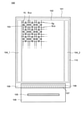
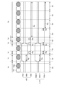
- the display device 100 includes a display area 102 and a peripheral area 109 provided on the substrate 101.
- the display area 102 has a plurality of pixels 103 arranged in a matrix.
- Each of the plurality of pixels 103 has a plurality of transistors and light emitting elements.
- the peripheral area 109 is provided so as to surround the display area 102.
- the peripheral region 109 refers to a region on the substrate 101 from the display region 102 to the end of the substrate 101. In other words, the peripheral region 109 refers to an region other than the display region 102 provided on the substrate 101 (that is, an region outside the display region 102).
- the peripheral region 109 includes gate drive circuits 104_1 and 104_2, a terminal portion 107 including a plurality of terminals 106, and a driver IC 105.
- the gate drive circuits 104_1 and 104_1 are provided so as to sandwich the display area 102.
- the driver IC 105 is connected to a plurality of terminals 106, and the plurality of terminals 106 are connected to a flexible printed circuit 108.
- FIG. 1 shows an example in which a source drive circuit is incorporated in the driver IC 105, but the present invention is not limited to this form, and a source drive circuit may be provided on the substrate 101 separately from the driver IC 105.
- the driver IC 105 is shown in an example in which it is arranged on the substrate 101 in the form of an IC chip, the driver IC 105 is not limited to this form and may be arranged in the flexible printed circuit 108.
- the driver IC 105 is connected to the gate drive circuits 104_1 and 104_1 and a plurality of video signal line VLs.
- the gate drive circuit 104_1 or the gate drive circuit 104_1 is connected to the pixel 103 via the write control scanning line Sg.
- the plurality of write control scan lines Sg for example, the odd-numbered line write control scan line Sg is connected to the gate drive circuit 104_1, and the even-numbered line write control scan line Sg is connected to the gate drive circuit 104_1.
- the video signal line VL is connected to the pixel 103.
- a control signal SG for selecting each pixel 103 is given to the display area 102 from the driver IC 105 via the gate drive circuits 104_1 and 104_2 and the write control scanning line Sg. Further, the video signal Vsig is given to the display area 102 from the driver IC 105 via the video signal line VL. By these signals, the transistor included in the pixel 103 can be driven to display an image in the display area 102 according to the video signal Vsig.
- the high-potential power supply SLa and the low-potential power supply electrode SLb connected to the pixel 103 are connected to different terminals 106, respectively.
- the substrate 101 a glass substrate or a flexible plastic substrate is used.
- a flexible plastic substrate is used as the substrate 101, the region between the display region 102 and the terminal portion 107 can be bent. As a result, the frame of the display device 100 can be narrowed.
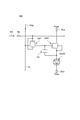
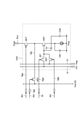
- FIG. 2 is an equivalent circuit diagram of pixels 103 included in the display device 100 according to the embodiment of the present invention.
- the display device 100 has a high-potential power supply SLa, a low-potential power supply electrode SLb, a write control scanning line Sg, and a video signal line VL.
- the high-potential power source SLa is given a high-potential power supply Pvdd
- the low-potential power supply electrode SLb is given a low-potential power supply Pvss.
- the write control scanning line Sg is connected to the gate drive circuits 104_1 and 104_1, and the video signal line VL is connected to the driver IC 105.
- Each pixel 103 has at least a drive transistor DRT, a write transistor SST, and a light emitting element OLED.
- the anode (also referred to as a pixel electrode) of the light emitting element OLED is provided with a high potential power supply Pvdd via the drive transistor DRT, and the cathode (also referred to as a common electrode) is provided with a low potential power supply Pvss.
- the drive transistor DRT is connected in series with the light emitting element OLED between the high-potential power supply SLa and the low-potential power supply electrode SLb.
- the drive transistor DRT functions as a current control element that controls the current value flowing through the light emitting element OLED according to the gate-source voltage.
- the write transistor SST functions as a switching element for selecting conduction or non-conduction between two nodes, and writes a voltage corresponding to the emission luminance of the light emitting element OLED.
- a holding capacitance Cs may be provided between the gate and the source of the drive transistor DRT. The holding capacitance Cs holds the gate-source voltage of the drive transistor DRT for a certain period of time.
- the write transistor SST has a first terminal, a second terminal, and a control terminal.
- the drive transistor DRT has a first terminal, a second terminal, a first control terminal, and a second control terminal.
- the first terminal will be described as a source electrode, the second terminal as a drain electrode, the first control terminal as a first gate electrode, and the second control terminal as a second gate electrode.
- the first gate electrode and the second gate electrode are connected to the write control scanning line Sg, the source electrode is connected to the video signal line VL, and the drain electrode is connected to the first gate electrode of the drive transistor DRT. Be connected.
- the drain electrode is connected to the high potential power supply SLa, and the source electrode is connected to one electrode (here, the anode) of the second gate electrode and the light emitting element OLED.
- the other electrode (here, the cathode) of the light emitting element OLED is connected to the low potential power supply electrode SLb.
- the drive transistor DRT outputs a drive current of a current amount corresponding to the video signal Vsig to the light emitting element OLED.
- amorphous silicon, low-temperature polysilicon, or oxide semiconductor is used as the semiconductor layer of the transistor constituting the display device 100.
- the transistor using the oxide semiconductor layer has a low off-leakage current and can be driven at a low frequency, it is possible to realize a display device 100 with low power consumption. Further, the transistor using the oxide semiconductor layer has better saturation characteristics than the transistor having the low temperature polysilicon layer because the kink effect is not observed. In this embodiment, a case where an oxide semiconductor layer is used as the semiconductor layer of the transistor constituting the display device 100 will be described.
- Transistors using an oxide semiconductor layer have the problem of low reliability, such as changes in the threshold voltage over time.
- a writing transistor and a driving transistor are formed in a dual gate structure in order to increase the on-current of a transistor using an oxide semiconductor layer
- a voltage applied to the oxide semiconductor layer is likely to be applied to the driving transistor.
- a large amount of current flows through the drive transistor.
- the oxide semiconductor layer is thermally deteriorated, and the reliability of the drive transistor is lowered.
- the on-current can be increased by forming the gate insulating film as thin as 100 nm or more and 200 nm or less, and the subthreshold swing value can be increased. (Hereinafter referred to as S value) can be reduced. Therefore, when a transistor having a top gate structure is used as a writing transistor, the effect that the switching characteristics are improved due to the small S value can be obtained. On the other hand, when a transistor having a top gate structure is used as a drive transistor, it is driven by a current, so that there is a problem that the current change becomes large due to a small S value.
- the transistor using the oxide semiconductor layer is formed with a bottom gate structure
- the voltage applied to the oxide semiconductor layer is less likely to be applied by increasing the thickness of the gate insulating film, so that the current flowing through the transistor is reduced. The amount can be reduced. Therefore, when a transistor having a bottom gate structure with a thick gate insulating film is used as a driving transistor, thermal deterioration of the oxide semiconductor layer is suppressed and the reliability of the transistor is improved.
- the on-current ion of the writing transistor decreases due to the thick gate insulating film. Tend.
- a transistor using an oxide semiconductor layer when applied to a display device, it is preferable to provide a transistor having different characteristics and structures according to a required function.
- a write transistor is provided with a transistor having good switching characteristics and a high on-current
- a drive transistor is provided with a transistor that is lower than the switching characteristics of a write transistor, suppresses thermal deterioration, and has high reliability. It is preferable to provide it.
- the write transistor SST having a switching function and the transistors constituting the gate drive circuits 104_1 and 104_1 are top gate driven or dual gate driven, and have a current control function.
- the drive transistor shall be bottom gate driven.
- the top gate drive is controlled to be turned on and off by a gate electrode arranged above the oxide semiconductor layer.
- the transistor for driving the top gate may have a top gate structure composed of gate electrodes arranged above the oxide semiconductor layer, or gate electrodes arranged above and below the oxide semiconductor layer. It may be a dual gate structure configured.
- the bottom gate drive is one in which on / off is controlled by a gate electrode arranged below the oxide semiconductor layer.
- the bottom gate drive transistor may have a bottom gate structure composed of gate electrodes arranged below the oxide semiconductor layer, or gate electrodes arranged above and below the oxide semiconductor layer. It may be a dual gate structure configured. Further, in the present specification, the dual gate drive means that on / off is controlled by inputting the same control signal to the gate electrodes arranged above and below the oxide semiconductor layer.
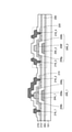
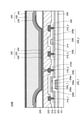
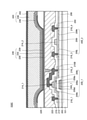
- FIG. 3 is a diagram illustrating a cross-sectional structure of a pixel 103 of a display device 100 according to an embodiment of the present invention.
- a transistor 210 and a transistor 220 are provided on the substrate 101 via a base film 202.
- the transistor 210 is connected to the light emitting element 230.
- the transistor 210 corresponds to the drive transistor DRT
- the transistor 220 corresponds to the write transistor SST
- the light emitting element 230 corresponds to the light emitting element OLED.
- the transistor 210 that functions as a drive transistor DRT has a dual gate structure.
- the transistor 210 includes a conductive layer 204_1, an insulating film 206 provided on the conductive layer 204_1, an oxide semiconductor layer 208_1 provided on the insulating film 206, and an insulating film 212 provided on the oxide semiconductor layer 208_1. And at least the conductive layer 214_1 provided on the insulating film 212.
- the first control terminal that controls the switching of the transistor 210 is the conductive layer 204_1. Therefore, the transistor 210 is bottom gate driven.
- the conductive layer 204_1 also functions as a light-shielding layer for suppressing the irradiation of the back surface of the oxide semiconductor layer 208 with light.
- the second control terminal is the conductive layer 214_1.
- the oxide semiconductor layer 208_1 has a channel region 208a and high-concentration impurity regions 208b and 208c.
- the high-concentration impurity regions 208b and 208c are provided with the channel region 208a interposed therebetween.
- the channel region 208a overlaps with the conductive layer 204_1.
- the insulating film 206 functions as a gate insulating film of the transistor 210.
- An insulating film 216 is provided on the oxide semiconductor layer 208_1.
- the insulating film 216 functions as an interlayer insulating film.
- a source electrode or a drain electrode 218_1 and 218_2 are provided on the insulating film 216.
- the source electrode or drain electrode 218_1 is connected to the high-concentration impurity region 208b via a contact hole provided in the insulating film 212 and 216.
- the source electrode or drain electrode 218_2 is connected to the high-concentration impurity region 208c and the conductive layer 214_1.
- the conductive layer 214_1 is connected to the pixel electrode 226 of the light emitting element OLED via the source electrode or the drain electrode 218_2.
- the conductive layer 204_1 is electrically connected to either the source electrode or the drain electrode 218_3 or 218_4.
- the connection of the conductive layer 214_1 may be connected to, for example, a fixed potential in addition to the embodiment shown in FIG. As an example of the fixed potential, there is a high potential power supply Pvdd, which is a drive power supply for the light emitting element OLED, a low potential power supply Pvss, or the like.
- the transistor 220 that functions as a write transistor SST has a dual gate structure.
- the transistor 220 includes a conductive layer 204_2, an insulating film 206 provided on the conductive layer 204_2, an oxide semiconductor layer 208_2 provided on the insulating film 206, and an insulating film 212 provided on the oxide semiconductor layer 208_2. And at least the conductive layer 214_2 provided on the insulating film 212.
- the first control terminals that control the switching of the transistor 220 are the conductive layer 204_2 and the conductive layer 214_2. Therefore, the transistor 220 is a dual gate drive.
- the conductive layer 204_1 also functions as a light-shielding layer for suppressing the irradiation of the back surface of the oxide semiconductor layer 208 with light.
- the insulating film 206 and the insulating film 212 function as a gate insulating film.
- the oxide semiconductor layer 208_2 has a channel region 208f and high-concentration impurity regions 208g and 208h.
- the high-concentration impurity regions 208g and 208h are provided with the channel region 208f interposed therebetween.
- the channel region 208f is superimposed on the conductive layer 214_2.
- An insulating film 216 is provided on the conductive layer 214_2.
- a source electrode or a drain electrode 218_3 and 218_4 are provided on the insulating film 216.
- the source electrode or drain electrode 218_3 and 218_4 are connected to the high-concentration impurity regions 208g and 208h via contact holes provided in the insulating films 212 and 216.
- a dual gate drive transistor having a dual gate structure is provided as a write transistor SST, and a bottom gate drive transistor having a dual gate structure is provided as a drive transistor DRT.
- a write transistor SST write transistor
- a bottom gate drive transistor having a dual gate structure is provided as a drive transistor DRT.
- the thickness of the gate insulating film can be made different between the writing transistor SST and the driving transistor DRT.
- the write transistor SST is configured as a dual gate drive, but the threshold voltage is dominated by the voltage applied by the conductive layer 214_2 provided via the thin insulating film 212.
- the gate insulating film of the write transistor SST can be made thinner than the gate insulating film of the drive transistor DRT, an electric field is likely to be applied to the oxide semiconductor layer 208_2, and the on-current can be increased. Further, in the writing transistor SST, since the impurity element is added to the oxide semiconductor layer 208_2 with the conductive layer 214_2 as a mask, the channel length L can be shortened. In one embodiment of the present invention, the channel length L of the write transistor SST and the drive transistor DRT can be, for example, 1.5 ⁇ m or more and 4.0 ⁇ m or less. As a result, the S value of the write transistor SST can be reduced, so that the switching characteristics of the write transistor SST are improved.
- the gate insulating film of the drive transistor DRT can be made thicker than the gate insulating film of the write transistor SST, it is difficult for an electric field to be applied to the oxide semiconductor layer 208_1, and the on-current of the drive transistor DRT is reduced. Can be done. Further, since the S value of the drive transistor DRT can be increased, the current change can be reduced in the low gradation region controlled by a minute current, and the gradation can be finely controlled. As a result, it is possible to suppress the occurrence of display unevenness in the display area 102. Further, since it is possible to suppress the continuous flow of a large amount of current through the drive transistor DRT, it is possible to suppress the deterioration of reliability due to thermal deterioration.
- the conductive layer 214_1 and the high-concentration impurity region 208c are connected via the source electrode or the drain electrode 218_2.
- the conductive layer 214_1 is connected to the pixel electrode 226 of the light emitting element OLED via the source electrode or the drain electrode 218_2.
- the gate drive circuits 104_1 and 104_1 can be driven at high speed.
- a flattening film 222 is provided on the source electrode or the drain electrode 218_1 to 218_4.
- an organic resin material such as polyimide, polyamide, acrylic, or epoxy can be used. These materials can form a film by a solution coating method and have a high flattening effect.
- the flattening film 222 is not provided in the peripheral region 109.
- the transistor 210 is connected to the light emitting element 230.
- the light emitting element 230 has a pixel electrode 226, an organic layer 232, and a common electrode 234.
- the display device 100 may be a top emission type or a bottom emission type. In the present embodiment, the case where the display device 100 has a top emission structure will be described. In the case of the top emission structure, the pixel electrode 226 serves as an anode and the common electrode 234 serves as a cathode.
- a pixel electrode 226 is provided on the flattening film 222.
- the pixel electrode 226 is provided for each pixel 103.
- the pixel electrode 226 is connected to the source electrode or the drain electrode 218_2 of the transistor 210 via a contact hole provided in the flattening film 222.
- a metal film having high reflectance is used as the pixel electrode 226.
- a laminated structure of a transparent conductive layer having a high work function such as an indium oxide-based transparent conductive layer (for example, ITO) or a zinc oxide-based transparent conductive layer (for example, IZO, ZnO) and a metal film can be used. can.
- An insulating layer 228 is provided so as to cover the end of the pixel electrode 226.
- the insulating layer 228 is also referred to as a partition wall or a bank.
- photosensitive acrylic is used as in the flattening film 222. It is preferable that the insulating layer 228 is opened so that the pixel electrode 226 is exposed, and the end portion of the opening has a gently tapered shape. If the end of the opening has a steep shape, poor coverage of the organic layer 232 formed later occurs.
- a plurality of organic materials constituting the organic layer 232 are laminated on the pixel electrode 226 and the insulating layer 228.
- the organic layer 232 is provided by laminating a hole transport layer, a light emitting layer, an electron transport layer, and the like in order from the pixel electrode 226 side. These layers may be formed by thin film deposition or may be formed by coating on solvent dispersion. Further, the hole transport layer, the electron transport layer, and the like may be selectively formed for each sub-pixel, or may be formed on the entire surface of the display region 102.
- a common electrode 234 is provided on the organic layer 232. In the present embodiment, since it has a top emission structure, the common electrode 234 needs to have translucency. When MgAg is used as the common electrode 234, it is formed of a thin film that allows the emitted light from the organic layer 232 to pass through.
- the common electrode 234 is connected to the wiring layer at the cathode contact portion provided in the peripheral region 109 and is electrically connected to the terminal 106.
- a sealing film 240 is provided on the common electrode 234.
- the sealing film 240 is provided to prevent moisture that has entered from the outside from entering the organic layer 232.
- an example of forming the sealing film 240 with a three-layer structure of an inorganic insulating layer 236, an organic insulating layer 238, and an inorganic insulating layer 242 is shown.
- silicon nitride having a high gas barrier property as the inorganic insulating layer 236 and 233
- an organic resin material having high flexibility as the organic insulating layer 238.
- a silicon oxide film or an amorphous silicon film may be provided between the silicon nitride and the organic resin material. This makes it possible to improve the adhesion between the silicon nitride and the organic resin material.
- an overcoat layer may be provided on the inorganic insulating layer 242 for flattening.
- a touch sensor 110 is provided on the sealing film 240.
- the touch sensor 110 may be formed directly on the sealing film 240.
- a cover glass on which the touch sensor 110 is formed may be provided on the sealing film 240.
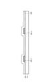
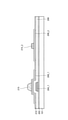
- FIG. 4 is a diagram illustrating a process of forming the base film 202 to the insulating film 206 on the substrate 101.
- a glass substrate, a quartz substrate, or a flexible substrate polyimide, polyethylene terephthalate, polyethylene naphthalate, triacetyl cellulose, cyclic olefin copolymer, cycloolefin polymer, or other flexible resin substrate
- polyimide polyethylene terephthalate, polyethylene naphthalate, triacetyl cellulose, cyclic olefin copolymer, cycloolefin polymer, or other flexible resin substrate
- the base film 202 is formed on the substrate 101. Silicon oxide or silicon nitride may be used as a single layer as the base film 202, or silicon oxide and silicon nitride may be used in combination in a laminated manner.
- Conductive layers 204_1 and 204_1 are formed on the base film 202.
- the conductive layers 204_1 and 204_1 are formed by forming a conductive film on the base film 202 and processing it by a photolithography method. Examples of the conductive layers 204_1 and 204_1 include aluminum (Al), titanium (Ti), chromium (Cr), cobalt (Co), nickel (Ni), zinc (Zn), molybdenum (Mo), copper (Cu), and indium.
- In tin (Sn), hafnium (Hf), tantalum (Ta), tungsten (W), platinum (Pt), bismuth (Bi) and the like can be used. Further, alloys of these metals may be used.
- the insulating film 206 is formed on the conductive layers 204_1 and 204_2.
- silicon oxide or silicon nitride may be used as a single layer, or silicon oxide and silicon nitride may be used in combination and laminated.
- the film thickness of the insulating film 206 is preferably larger than the film thickness of the insulating film 212, which will be described later.
- the film thickness of the insulating film 206 is preferably formed to be, for example, 250 nm or more and 500 nm or less.
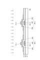
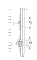
- FIG. 5 is a diagram illustrating a process of forming the oxide semiconductor layers 208_1 and 208_2 to the conductive layers 214_1 and 214_2 on the insulating film 206.
- the oxide semiconductor layers 208_1 and 208_2 are formed on the insulating film 206.
- the oxide semiconductor layers 208_1 and 208_2 are formed by forming an oxide semiconductor film by a sputtering method and processing it by a photolithography method.
- the oxide semiconductor film is preferably formed with a film thickness of 30 nm or more and 100 nm or less by, for example, a sputtering method.
- the oxide semiconductor layers 208_1 and 208_2 may contain Group 13 elements such as indium and gallium.
- the oxide semiconductor layers 208_1 and 208_2 may further contain Group 12 elements, and examples thereof include compounds containing indium, gallium, and zinc (IGZO).
- the oxide semiconductor layers 208_1 and 208_2 may contain other elements, and may contain tin which is a Group 14 element, titanium and zirconium which are Group 4 elements, and the like.
- oxide semiconductor layers 208_1 and 208_1 are InO x , ZnO x , SnOx, In—Ga—O, In—Zn—O, In—Al—O, In—Sn—O, and In—Hf ⁇ .
- the crystallinity of the oxide semiconductor layers 208_1 and 208_1 is not limited, and may be single crystal, polycrystal, microcrystal, or amorphous.
- the power source applied to the oxide semiconductor target may be a direct current (DC) or an alternating current power source (AC), and can be determined by the shape and composition of the oxide semiconductor target.
- oxygen gas As the sputtering gas for forming the oxide semiconductor film, oxygen gas, a mixed gas of oxygen and a rare gas, or a rare gas can be used.
- the sputtering gas for forming the oxide semiconductor film it is preferable to carry out the sputtering gas in a mixed gas atmosphere of oxygen and a rare gas, and it is more preferable that the oxygen gas flow rate ratio to the rare gas is 5% or more. It is preferable to set the oxygen gas flow rate ratio to 5% or more because oxygen is easily added to the oxide semiconductor film.
- the insulating film 212 is formed on the oxide semiconductor layers 208_1 and 208_2.
- Silicon oxide or silicon nitride may be used as a single layer as the insulating film 212, or silicon oxide and silicon nitride may be used in combination in a laminated manner.
- the film thickness of the insulating film 212 is preferably smaller than the film thickness of the insulating film 206.
- the film thickness of the insulating film 212 is preferably formed to be, for example, 100 nm or more and 200 nm or less.
- the heat treatment may be performed at least once after the oxide semiconductor film is formed, the oxide semiconductor layers 208_1 and 208_2 are formed, or the insulating film 212 is formed. Since the volumes of the oxide semiconductor layers 208_1 and 208_2 may be reduced (shrinked) by the heat treatment, it is preferable to perform the heat treatment before the processing by the photolithography method.
- the hydrogen concentration of the oxide semiconductor layers 208_1 and 208_2 is subjected to heat treatment at least once after the oxide semiconductor film is formed, the oxide semiconductor layers 208_1 and 208_2 are formed, or after the insulating film 212 is formed. It is possible to improve the film quality, such as reducing the amount of oxides and improving the density.
- the heat treatment performed on the oxide semiconductor film or the oxide semiconductor layers 208_1 and 208_2 can be performed at atmospheric pressure or low pressure (vacuum) in the presence of nitrogen, dry air, or the atmosphere.
- the heating temperature is 250 ° C. to 500 ° C., preferably 350 ° C. to 450 ° C.
- the heating time is, for example, 15 minutes or more and 1 hour or less.
- oxygen is introduced into the oxygen deficiency of the oxide semiconductor layers 208_1 and 208_2 or oxygen is dislocated, so that the oxide semiconductor layers 208_1 and 208_2 having few crystal defects and high crystallinity can be obtained. Further, the hydrogen concentration of the oxide semiconductor layers 208_1 and 208_1 can be reduced by the heat treatment.
- the conductive layers 214_1 and 214_2 are formed on the insulating film 212.
- the conductive layers 214_1 and 214_1 are formed by forming a conductive film on the insulating film 212 and processing it by a photolithography method.
- the conductive layers 214_1 and 214_1 for example, the same materials as those of the conductive layers 204_1 and 204_1 can be used.
- the conductive layer 214_1 is formed in a region overlapping the conductive layer 204_1 and the oxide semiconductor layer 208_1, and the conductive layer 214_1 is formed in a region overlapping the conductive layer 204_1 and the oxide semiconductor layer 208_1.
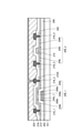
- FIG. 6 is a diagram illustrating a step of adding an impurity element to the oxide semiconductor layers 208_1 and 208_2 by ion implantation.
- Impurity elements are added to the oxide semiconductor layers 208_1 and 208_1 by ion implantation using the conductive layers 214_1 and 214_1 as masks.
- hydrogen, argon, phosphorus, boron or the like is used as the impurity element. Since the addition of the impurity element to the oxide semiconductor layer is not intended to control the conductive type of the transistor, the type of the impurity element is not particularly limited.
- the concentration (dose amount) of the impurity element is set to 1 ⁇ 10 14 atoms / cm 2 to 5 ⁇ 10 15 atoms / cm 2 and added to the oxide semiconductor layers 208_1 and 208_2.
- the high-concentration impurity regions 208b and 208c are formed in the region that does not overlap with the conductive layer 214_1, and the channel region 208a is formed in the region that overlaps with the conductive layer 214_1.
- high-concentration impurity regions 208g and 208h are formed in a region that does not overlap with the conductive layer 214_2, and a channel region 208f is formed in a region that overlaps with the conductive layer 214_2.
- the high-concentration impurity regions 208b, 208c, 208g, 208h contain impurity elements at a concentration of about 5 ⁇ 10 13 atoms / cm 3 to 2.5 ⁇ 10 15 atoms / cm 3 .
- the concentration of the impurity element contained in the oxide semiconductor layers 208_1 and 208_1 can be measured by, for example, a secondary ion mass spectrometry (SIMS).
- the oxide semiconductor layers 208_1 and 208_2 By adding an impurity element to the oxide semiconductor layers 208_1 and 208_2, defects occur in the crystals of the oxide semiconductor layers 208_1 and 208_2, so that the resistance in the region is reduced.
- the resistance of the oxide semiconductor layers 208_1 and 208_2 can be reduced depending on the concentration of the added impurity element.
- the channel regions 208a and 208f have few crystal defects and a low hydrogen concentration, so that the resistance remains high. In this way, the resistance of the high-concentration impurity regions 208b, 208c, 208g, 208h can be made lower than the resistance of the channel regions 208a, 208f.
- FIG. 7 is a diagram illustrating a step of forming the source electrode or the drain electrode 218_1 to 218_4 from the insulating film 216 on the oxide semiconductor layers 208_1 and 208_2.
- the insulating film 216 is formed on the oxide semiconductor layers 208_1 and 208_2.
- silicon oxide or silicon nitride may be used as a single layer, or silicon oxide and silicon nitride may be combined and laminated.
- the film thickness of the insulating film 216 is preferably larger than the film thickness of the insulating film 212.
- the thickness of the insulating film 216 is preferably formed to be, for example, 250 nm or more and 500 nm or less.
- the source electrode or the drain electrode 218_1 to 218_4 is formed on the insulating film 216.
- the source electrode or drain electrode 218_1 to 218_4 is formed by forming a conductive film on the insulating film 216 and processing the conductive film by a photolithography method. As a result, the source electrode or drain electrode 218_1 is connected to the high-concentration impurity region 208b, and the source electrode or drain electrode 218_1 is connected to the high-concentration impurity region 208c and the conductive layer 214_1.
- the source electrode or drain electrode 218_3 is connected to the high concentration impurity region 208g, and the source electrode or drain electrode 218_4 is connected to the high concentration impurity region 208h.
- the same material as the conductive layers 204_1 and 204_2 can be used.
- contact holes that reach the conductive layer 204_1 may be formed in the insulating films 206, 212, and 216 during this step. Thereby, the conductive layer 204_1 can be connected to the source electrode or the drain electrode 218_3.
- the transistors 210 and 220 can be formed.
- FIG. 8 is a diagram illustrating a process of forming the flattening film 222 and the pixel electrode 226.
- a flattening film 222 is formed on the source or drain electrodes 218_1 to 218_4.
- an organic resin material such as polyimide, acrylic, or epoxy can be used. These materials are characterized in that a film can be formed by a solution coating method and a flattening effect is high.
- the light emitting element 230 is formed by forming the pixel electrode 226, the organic layer 232, and the common electrode 234. First, a contact hole that reaches the source electrode or the drain electrode 218_2 is formed in the flattening film 222. Next, the pixel electrode 226 is formed on the flattening film 222. The pixel electrode 226 is formed by forming a conductive film on the flattening film 222 and processing the conductive film by a photolithography method. An insulating layer 228 is formed so as to expose the pixel electrode 226. Next, a plurality of organic materials constituting the organic layer 232 are formed on the pixel electrode 226 and the insulating layer 228. Next, the common electrode 234 is formed on the organic layer 232.
- the sealing film 240 is formed by forming the inorganic insulating layer 236, the organic insulating layer 238, and the inorganic insulating layer 242 on the common electrode 234.
- the inorganic insulating layer 236 is formed on the common electrode 234.
- the organic insulating layer 238 is formed on the inorganic insulating layer 236.
- the inorganic insulating layer 242 is formed on the organic insulating layer 238.
- the display device 100 having the configuration of the pixel 103 shown in FIG. 3 can be manufactured.
- two types of transistors having different characteristics and structures can be more easily produced without increasing the process even in a small area of one pixel. Can be formed.
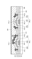
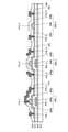
- FIG. 9 is a diagram illustrating a cross-sectional structure of the pixel 103A of the display device 100 according to the embodiment of the present invention.
- the transistor 210 and the transistor 250 are provided on the substrate 101 via the base film 202.
- the transistor 210 corresponds to the drive transistor DRT shown in FIG. 3
- the transistor 250 corresponds to the write transistor SST shown in FIG. Since the structure of the transistor 210 is the same as that of the transistor 210 shown in FIG. 3, the description thereof will be omitted.
- the transistor 250 that functions as a write transistor SST has a top gate structure.
- the transistor 250 has at least an oxide semiconductor layer 208_3 provided on the insulating film 206, an insulating film 212 provided on the oxide semiconductor layer 208_3, and a conductive layer 214_3 provided on the insulating film 212. ..
- the control terminal that controls the switching of the transistor 250 is the conductive layer 214_3.
- the insulating film 212 functions as a gate insulating film.
- the oxide semiconductor layer 208 has a channel region 208i and high-concentration impurity regions 208j and 208k.
- An insulating film 212 is provided on the conductive layer 214_3.
- a source electrode or a drain electrode 218_5 and 218_6 are provided on the insulating film 212.
- the source electrode or drain electrode 218_5, 218_6 is connected to the high-concentration impurity regions 208j and 208k via contact holes provided in the insulating film 212 and 216.
- the gate insulating film of the write transistor SST can be made thinner than the gate insulating film of the drive transistor DRT, an electric field is likely to be applied to the oxide semiconductor layer 208_3, and the on-current can be increased. Further, since the channel length L can be shortened, the switching characteristics are improved. On the other hand, since the gate insulating film of the drive transistor DRT can be made thicker than the gate insulating film of the write transistor SST, it is difficult for an electric field to be applied to the oxide semiconductor layer 208_1, and the on-current can be reduced. In particular, in a low gradation region controlled by a minute current, the current change of the drive transistor DRT can be made small, so that the gradation can be finely controlled.
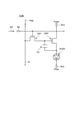
- FIG. 10 is an equivalent circuit diagram of the pixel 103B included in the display device 100 according to the embodiment of the present invention.
- the difference from the equivalent circuit diagram shown in FIG. 2 is the configuration of the drive transistor DRT.
- the drive transistor DRT is bottom gate driven and the write transistor SST is top gate drive.
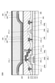
- FIG. 11 is a diagram illustrating a cross-sectional structure of the pixel 103B of the display device 100 according to the embodiment of the present invention.
- the transistor 210A and the transistor 250 are provided on the substrate 101 via the base film 202.
- the transistor 250 corresponds to the write transistor SST shown in FIG. 10
- the transistor 210A corresponds to the drive transistor DRT shown in FIG. Since the structure of the transistor 250 is the same as the structure of the transistor 250 shown in FIG. 9, detailed description thereof will be omitted.
- the transistor 210A that functions as a drive transistor DRT has a bottom gate structure.
- the transistor 210A has at least a conductive layer 204_1, an insulating film 206 provided on the conductive layer 204_1, and an oxide semiconductor layer 208_1 provided on the insulating film 206.
- the oxide semiconductor layer 208_1 has a channel region 208a, high-concentration impurity regions 208b and 208c, and low-concentration impurity regions 208d and 208e.
- the low-concentration impurity regions 208d and 208e are provided with the channel region 208a interposed therebetween.
- the high-concentration impurity regions 208b and 208c are provided adjacent to the low-concentration impurity regions 208d and 208e.
- the channel region 208a and the low-concentration impurity regions 208d and 208e are superimposed on the conductive layer 204_1.
- the insulating film 206 functions as a gate insulating film of the transistor 210.
- An insulating film 212 is provided on the oxide semiconductor layer 208_1, and an insulating film 216 is further provided on the insulating film 212.
- the film thickness of the insulating film 206 is preferably larger than the film thickness of the insulating film 212.
- the film thickness of the insulating film 206 is 250 nm or more and 500 nm or less.
- the film thickness of the insulating film 212 is 100 nm or more and 200 nm or less.
- a source electrode or a drain electrode 218_1 and 218_2 are provided on the insulating film 216.
- the source electrode or drain electrode 218_1 and 218_2 are connected to the high-concentration impurity regions 208b and 208c via contact holes provided in the insulating films 212 and 216.
- the conductive layer 204_1 is electrically connected to either the source electrode or the drain electrode 218_3 or 218_4.
- low-concentration impurity regions 208d and 208e are provided between the channel regions 208a and the high-concentration impurity regions 208b and 208c in the oxide semiconductor layer 208_1.
- the electric field applied in the vicinity of the end of the channel region 208a becomes small, so that the source / drain resistance can be improved.
- the source / drain resistance can be further improved.
- a transistor having a top gate structure is provided as a writing transistor SST, and a transistor having a bottom gate structure is provided as a driving transistor DRT on the same substrate.
- the insulating film 212 functions as a gate insulating film in the writing transistor SST, and the insulating film 206 is used in the drive transistor DRT. Functions as a gate insulating film.
- the film thickness of the insulating film 212 is smaller than the film thickness of the insulating film 206.
- the thickness of the gate insulating film can be made different between the writing transistor SST and the driving transistor DRT. That is, a thin gate insulating film can be applied to the SST driven by the top gate, and a thick gate insulating film can be applied to the drive transistor DRT driven by the bottom gate.
- the gate insulating film of the write transistor SST can be made thinner than the gate insulating film of the drive transistor DRT, an electric field is likely to be applied to the oxide semiconductor layer 208_2, and the on-current can be increased. Further, in the writing transistor SST, since the impurity element is added to the oxide semiconductor layer 208_2 via the conductive layer 214_2, the channel length L can be shortened. As a result, the S value of the write transistor SST can be reduced. On the other hand, since the gate insulating film of the drive transistor DRT can be made thicker than the gate insulating film of the write transistor SST, it is difficult for an electric field to be applied to the oxide semiconductor layer 208_1, and the on-current can be reduced.
- the current change of the drive transistor DRT can be made small, so that the gradation can be finely controlled.
- the gradation can be finely controlled.
- it is possible to suppress the continuous flow of a large amount of current through the drive transistor DRT it is possible to suppress the deterioration of reliability due to thermal deterioration.
- the BT stress of the gate becomes larger than the case where the one-side gate drive is performed. Therefore, although there is an advantage that the on / off characteristics of the transistor are sharpened, reliability may be sacrificed to some extent. Therefore, when the drive capacity is sufficient for the top gate drive and the back surface does not need to be shielded from light, the reliability can be improved by omitting the gate electrode on the bottom side.
- FIGS. 12 to 15 a method of manufacturing the display device 100 according to the embodiment of the present invention will be described with reference to FIGS. 12 to 15. From the step of forming the base film 202 on the substrate 101 to the step of forming the insulating film 212, the description of FIGS. 4 and 5 may be referred to.
- FIG. 12 is a diagram illustrating a process of forming the conductive layer 214_2 and the resist mask 215 on the insulating film 212.
- the conductive layer 214_2 is formed on the insulating film 212.
- the conductive layer 214_4 is formed by forming a conductive film on the insulating film 212 and processing it by a photolithography method.
- the conductive layer 214_2 is formed in a region overlapping with the oxide semiconductor layer 208_2.
- the resist mask 215 is formed in a part of the region that overlaps with the oxide semiconductor layer 208_1 provided on the insulating film 212.
- the resist mask 215 is formed so that the end portion has a tapered shape.
- the resist mask 215 is not limited to a tapered shape as long as the film thickness decreases as it approaches the end portion.
- FIG. 13 is a diagram illustrating a step of adding an impurity element to the oxide semiconductor layers 208_1 and 208_2 by ion implantation.
- impurity elements are added to the oxide semiconductor layers 208_1 and 208_2 by ion implantation.
- the concentration of the impurity element is set to 1 ⁇ 10 14 atoms / cm 2 to 5 ⁇ 10 15 atoms / cm 2 and added to the oxide semiconductor layers 208_1 and 208_2.
- the high-concentration impurity regions 208g and 208h are formed in the region that does not overlap with the conductive layer 214_2, and the channel region 208f is formed in the region that overlaps with the conductive layer 214_2.
- the high-concentration impurity regions 208 g and 208 h contain impurity elements at a concentration of about 5 ⁇ 10 13 atoms / cm 3 to 2.5 ⁇ 10 15 atoms / cm 3 .
- high-concentration impurity regions 208b and 208c are formed in the regions where the resist mask 215 does not overlap.
- the impurity element is added to the region where the resist mask 215 overlaps with the tapered shape via the resist mask 215, the low-concentration impurity regions 208d and 208e are formed. Further, a channel region 208a is formed in a region of the resist mask 215 that overlaps with a portion other than the tapered shape.
- the high-concentration impurity regions 208b and 208c contain impurity elements at a concentration of about 5 ⁇ 10 13 atoms / cm 3 to 2.5 ⁇ 10 15 atoms / cm 3 .
- the impurity elements are added to the low-concentration impurity regions 208d and 208e via the resist mask 215, the impurity elements are about 2.5 ⁇ 10 12 atoms / cm 3 to 5 ⁇ 10 13 atoms / cm 3 . Included in concentration.
- the oxide semiconductor layers 208_1 and 208_2 By adding an impurity element to the oxide semiconductor layers 208_1 and 208_2, defects occur in the crystals of the oxide semiconductor layers 208_1 and 208_2, so that the resistance in the region is reduced.
- the resistance of the oxide semiconductor layers 208_1 and 208_2 can be reduced depending on the concentration of the added impurity element. Therefore, the resistance of the high-concentration impurity regions 208b, 208c, 208g, 208h can be lower than the resistance of the low-concentration impurity regions 208d, 208e.
- the resist mask 215 having a tapered shape and the conductive layer 214_2 as masks, a structure having low-concentration impurity regions 208d and 208e is formed in the oxide semiconductor layer 208_1 in one step of adding an impurity element. Therefore, the oxide semiconductor layer 208_2 can be formed with a structure having no low-concentration impurity region.
- the channel regions 208a and 208f have few crystal defects and a low hydrogen concentration, so that the resistance remains high. In this way, different oxide semiconductor layers 208_1 and 208_2 can be formed in the same process. After adding the impurity element, the resist mask 215 is removed.
- FIG. 14 is a diagram illustrating a step of forming the pixel electrode 226 from the step of forming the insulating film 216.
- the description in FIG. 8 may be referred to.
- the manufacturing method described in the first embodiment may be applied.
- the display device 100 having the configuration of the pixel 103B shown in FIG. 11 can be manufactured.
- the oxide semiconductor layer 208_1 containing the high-concentration impurity regions 208b and 208c and the low-concentration impurity regions 208d and 208e and the oxide semiconductor layer 208_1 containing the high-concentration impurity regions 208g and 208h can be formed at the same time.
- FIG. 15 is a diagram illustrating a cross-sectional structure of the pixel 103C of the display device 100 according to the embodiment of the present invention.
- the transistor 210B and the transistor 250 are provided on the substrate 101 via the base film 202.
- the transistor 250 corresponds to the write transistor SST shown in FIG. 10
- the transistor 210B corresponds to the drive transistor DRT shown in FIG.
- the conductive layer 214_1 and the high-concentration impurity region 208b are connected to each other via the source electrode or the drain electrode 218_2 in the configuration of the transistor 210A.
- the impurity elements are added in an amount of about 5 ⁇ 10 12 atoms / cm 2 to 1 ⁇ 10 14 atoms / cm 2 using the conductive layers 214_1 and 214_1 as masks.
- the impurity element is added in an amount of about 1 ⁇ 10 14 atoms / cm 2 to 5 ⁇ 10 13 atoms / cm squared .
- the channel region 208a, the high-concentration impurity regions 208b, 208c, and the low-concentration impurity regions 208d, 208e may be formed on the oxide semiconductor layer 208_1 of the drive transistor DRT.
- FIG. 16 is an equivalent circuit diagram of the pixel 103E included in the display device 100 according to the embodiment of the present invention.
- the display device 100 has a high-potential power supply SLa, a low-potential power supply electrode SLb, a light emission control scanning line Sga, a writing control scanning line Sgb, a reset control scanning line Sgc, and a video signal line VL.
- the high-potential power source SLa is given a high-potential power supply Pvdd
- the low-potential power supply electrode SLb is given a low-potential power supply Pvss.
- the light emission control scan line Sga, the write control scan line Sgb, and the reset control scan line Sgc are connected to the gate drive circuits 104_1 and 104_1. Further, the video signal line VL is connected to the driver IC 105.
- Pixel 103E has a write transistor SST, a drive transistor DRT, a holding capacity Cs, and an additional capacity CAD.
- the holding capacity Cs and the additional capacity Cad are capacitors.
- the additional capacitance CAD is an element provided for adjusting the amount of light emission current, and may not be necessary in some cases.
- the parasitic capacitance Cel is the capacitance of the light emitting element itself (the parasitic capacitance of the light emitting element OLED).
- the light emitting element OLED also functions as a capacitor.
- Each pixel 103E has an output transistor BCT.
- the four pixels 103E adjacent to each other in the row direction X and the column direction Y share one output transistor BCT.
- the gate drive circuits 104_1 and 104_2 are provided with a plurality of reset transistors RST.
- the reset transistor RST and the reset control scanning line Sgr are connected one-to-one.
- the drive transistor DRT has the structure of the transistor 210 shown in the first embodiment, and the write transistor SST, the output transistor BCT, and the reset transistor RST have the structure of the transistor 220 shown in the first embodiment. There is. Alternatively, the drive transistor DRT has the structure of the transistor 210A or the transistor 210B shown in the second embodiment, and the write transistor SST, the output transistor BCT, and the reset transistor RST are the transistor 220 or the transistor 250 shown in the second embodiment. It may have the structure of. In the display device 100 according to the present embodiment, each drive transistor and each transistor constituting each switch are formed in the same process.
- Each of the write transistor SST, the drive transistor DRT, the output transistor BCT, and the reset transistor RST has a first terminal, a second terminal, and a control terminal.
- the first terminal is a source electrode
- the second terminal is a drain electrode
- the control terminal is a gate electrode.
- the drive transistor DRT is connected in series with the light emitting element OLED between the high potential power supply SLa and the low potential power supply electrode SLb.
- the drain electrode is connected to the high potential power supply SLa, the source electrode is connected to the drain electrode of the drive transistor DRT, and the gate electrode is connected to the light emission control scanning line Sga.
- the output transistor BCT is controlled on (conducting state) and off (non-conducting state) by the control signal BG (1 to m / 2) from the light emission control scanning line Sga.
- the output transistor BCT controls the light emission time of the light emitting element OLED in response to the control signal BG.
- the drain electrode is connected to the source electrode of the output transistor BCT and the reset control scanning line Sgr, and the source electrode is connected to one electrode (here, the anode) of the light emitting element OLED.
- the other electrode (here, the cathode) of the light emitting element OLED is connected to the low potential power supply electrode SLb.
- the drive transistor DRT outputs a drive current of a current amount corresponding to the video signal Vsig to the light emitting element OLED.
- the source electrode is connected to the video signal line VL (1 to n)
- the drain electrode is connected to the gate electrode of the drive transistor DRT
- the gate electrode is a write control that functions as a gate wiring for signal write control. It is connected to the scanning line Sgb (1 to m).
- the write transistor SST is turned on and off by a control signal SG (1 to m) supplied from the write control scan line Sgb. Then, the write transistor SST controls the connection / non-connection between the pixel circuit and the video signal line VL (1 to n) in response to the control signal SG (1 to m), and the corresponding video signal line VL ( The video signal Vsig is taken into the pixel circuit from 1 to n).
- the reset transistor RST is provided in the gate drive circuits 104_1 and 104_1 every two rows.
- the reset transistor RST is connected between the drain electrode of the drive transistor DRT and the reset power supply.
- the source electrode is connected to the reset power supply line SLc connected to the reset power supply
- the drain electrode is connected to the reset control scanning line Sgr
- the gate electrode is the reset control scanning line Sgc that functions as a gate wiring for reset control. It is connected to the.
- the reset power supply line SLc is connected to the reset power supply and fixed to the reset potential Vrst which is a constant potential.
- the reset transistor RST is in a conductive state (on) or a non-conducting state (off) between the reset power supply line SLc and the reset control scanning line Sgr according to the control signal RG (1 to m / 2) given through the reset control scanning line Sgc. ). By switching the reset transistor RST to the ON state, the potential of the source electrode of the drive transistor DRT is initialized.
- the gate drive circuits 104_1 and 104_1 include shift registers, output buffers, etc. (not shown), sequentially transfer the horizontal scan start pulse supplied from the outside to the next stage, and control three types to the pixel 103E of each row via the output buffer.
- the signals that is, the control signal BG (1 to m / 2), the control signal SG (1 to m), and the control signal RG (1 to m / 2) are supplied.
- the control signal RG is not directly supplied to the pixel 103E, a predetermined voltage is supplied from the reset power supply line SLc fixed to the reset potential Vrst at a predetermined timing according to the control signal RG.
- the light emission control scan line Sga, the write control scan line Sgb, and the reset control scan line Sgc are driven by the control signals BG, SG, and RG, respectively.
- FIG. 17 is a gate drive circuit 104_1 and 104_2 timing chart for driving the pixel shown in FIG.
- FIG. 17 shows the control signal RGk, the control signal BGk, and the control signal SGk on the k-line, and the control signal RGk + 1, the control signal BGk + 1, and the control signal SGk + 1 on the k + 1 line.
- Each section indicated by G1 to G4 is one horizontal period, and although omitted thereafter, it continues until the last line. The period indicated by T0 to in FIG. 16 will be described in detail below.
- DRT source initialization operation In this period, the control signal BG becomes L level, the control signal RG becomes H level, the control signal SG becomes L level, the output transistor BCT is turned off, the reset transistor RST is turned on, and the write transistor SST is turned off.
- the holding capacity Cs holds "a voltage corresponding to the video signal written in the previous frame". If the video signal Vsig is larger than the reset potential Vrst, the source side also approaches the reset potential Vrst through the drive transistor DRT. Further, since the reset potential Vrst has almost the same potential as the low potential power supply Pvss, the current supply to the light emitting element OLED is stopped. As a result, the potential on the source side of the drive transistor DRT becomes the lowest state in the pixel system.
- DRT gate initialization> During this period, the control signal BG is at L level, the control signal RG is at H level, the control signal SG is at H level, the video signal line VL is at the initialization potential Vini, the output transistor BCT is turned off, the reset transistor RST is turned on, and so on.
- the write transistor SST turns on.
- the gate of the drive transistor DRT is fixed to the initialization potential Vini via the write transistor SST.
- the initialization potential Vini is set to a potential larger than the threshold value of the drive transistor DRT with respect to the reset potential Vrst. That is, by this operation, the drive transistor DRT is turned on.
- the source of the drive transistor DRT is charged by the current supplied from the high potential power supply Pvdd, and its potential rises.
- the drive transistor DRT since the gate potential of the drive transistor DRT is Vini, the drive transistor DRT is turned off when the source of the drive transistor DRT becomes (Vini-Vth), and the increase in potential stops. Since Vth is the threshold voltage of the drive transistor DRT and varies depending on the pixel 103E, the potential of the source of the drive transistor DRT when the increase in potential is stopped differs depending on the pixel. That is, by this operation, a voltage corresponding to the threshold voltage of the drive transistor DRT is acquired in each pixel 103E.
- the control signal BG is H level
- the control signal RG is L level
- the control signal SG is H level
- the video signal line VL is the video signal Vsig
- the output transistor BCT is turned on
- the reset transistor RST is turned off
- the write transistor SST is set. Turn on.
- the video signal Vsig is input to the gate of the drive transistor DRT, and the gate potential of the drive transistor DRT changes from the initialization potential Vini to the video signal Vsig.
- the source potential of the drive transistor DRT is still (Vini-Vth), and as a result, the gate-source voltage of the drive transistor DRT becomes ⁇ Vsig- (Vini-Vth) ⁇ , which is the threshold value between the pixels 103E. The variation is reflected.
- the video signal writing operation is sequentially performed line by line.
- Luminous operation The control signal BG becomes H level, the control signal RG becomes L level, the control signal SG becomes L level, the output transistor BCT is turned on, the reset transistor RST is turned off, and the write transistor SST is turned off.
- a current is supplied from the high potential power supply Pvdd to the drive transistor DRT through the output transistor BCT.
- the drive transistor DRT causes a current corresponding to the gate-source voltage set up to the previous stage to flow through the light emitting element OLED, and the light emitting element OLED emits light with brightness corresponding to the current.
- the voltage between the anode and the cathode of the light emitting element OLED becomes a voltage corresponding to the current, so that the potential on the anode side rises, but the voltage between the gate and the source of the drive transistor DRT is maintained by the holding capacitance Cs. Therefore, as the potential on the anode side rises, the gate potential of the drive transistor DRT also rises due to the coupling of the holding capacitance Cs. Actually, since the gate of the drive transistor DRT has not only the holding capacitance Cs but also the additional capacitance Cad and other parasitic capacitances, the gate potential of the drive transistor DRT is higher than the potential increase on the anode side. Although the rise is slightly smaller, since this value is known, the potential of the video signal Vsig may be determined so as to obtain a desired current value at the gate-source voltage of the final drive transistor DRT.
- any one of the bottom gate drive transistors 210, 210A, 210B described in the first embodiment and the second embodiment is applied to the drive transistor DRT.
- any of the top gate drive transistors 220 and 250 described in the first embodiment and the second embodiment is applied to the reset transistor RST, the initialization transistor IST, and the like in addition to the write transistor SST.
- the S value of the drive transistor DRT is large, the current change of the drive transistor DRT can be reduced in the low gradation region where it is necessary to control with a minute current, and the gradation can be finely controlled. ..
- display unevenness can be suppressed in the display area 102.
- FIG. 18 is an equivalent circuit diagram of a pixel circuit of pixel 103F.
- the light emission control scan line Sga, the write control scan line Sgb, the reset control scan line Sgc, and the initialization control scan line Sgd are connected to the gate drive circuits 104_1 and 104_1 provided outside the display area 102, respectively.
- Each pixel 103F is provided with an output transistor BCT, an initialization transistor IST, a write transistor SST, and a drive transistor DRT. Some transistors may be shared between a plurality of adjacent pixels 103F.
- One reset transistor RST is provided outside the display area, for example, one for each row.
- a holding capacitance Cs may be provided between the gate and the source of the drive transistor DRT.
- the parasitic capacitance Cel is the parasitic capacitance between the anode and the cathode of the light emitting element OLED.
- a high potential power supply Pvdd is given to the anode of the light emitting element OLED via an output transistor BCT and a drive transistor DRT, and a low potential power supply Pvss is given to the cathode.
- the output transistor BCT, the initialization transistor IST, and the write transistor SST function as a switching element that selects conduction or non-conduction between the two nodes, and the drive transistor DRT flows to the OLED according to the gate-source voltage. It functions as a current control element that controls the current value.
- the transistor 210 is applied as the drive transistor DRT
- the structure of the transistor 220 is applied as the output transistor BCT, the initialization transistor IST, and the write transistor SST.
- FIG. 19 is a timing chart of the gate drive circuits 104_1 and 104_2 for driving the pixels shown in FIG.
- Each section indicated by G1 to G3 is one horizontal period and continues until the last line. The period represented by T0 to T6 in FIG. 19 will be described below.
- the reset potential Vrst has almost the same potential as the low potential power supply Pvss, the current supply to the light emitting element OLED is stopped. As a result, the potential on the source side of the drive transistor DRT becomes the lowest state in the pixel system.
- Gate initialization of drive transistor DRT> The control signal IG becomes H level, and the initialization transistor IST turns on. In each pixel of the row, the gate of the drive transistor DRT is fixed to the initialization potential Vini via the initialization transistor IST. The initialization potential Vini is set to a potential larger than the threshold value of the drive transistor DRT with respect to the reset potential Vrst. That is, by this operation, the drive transistor DRT is turned on. However, since the output transistor BCT is off, no current flows through the drive transistor DRT yet.
- the control signal BG is at H level
- the control signal RG is at L level
- the control signal IG is at H level
- the output transistor BCT is turned on
- the reset transistor RST is turned off
- the initialization transistor IST is turned on. Since the drive transistor DRT is turned on by the previous operation, a current is supplied from Pvdd to the drive transistor DRT through the output transistor BCT. At this stage, the voltage between the anode and the cathode of the light emitting element OLED does not exceed the light emission start voltage, so no current flows. Therefore, the source of the drive transistor DRT is charged by the current supplied from the high potential power supply Pvdd, and its potential rises.
- the drive transistor DRT since the gate potential of the drive transistor DRT is the initialization potential Vini, the drive transistor DRT is turned off when the source of the drive transistor DRT becomes (Vini-Vth), and the increase in potential stops.
- Vth is the threshold voltage of the drive transistor DRT, and since it varies depending on the pixel 103F, the potential of the source of the DRT when the increase in potential is stopped differs depending on the pixel. That is, by this operation, a voltage corresponding to the threshold voltage of the drive transistor DRT is acquired in each pixel.
- T1. ⁇ T3. The operation of is performed in parallel for two lines, but this is not the case. It may be carried out sequentially for each line, or three or more lines may be carried out in parallel.
- the control signal BG is H level
- the control signal RG is L level
- the control signal IG is L level
- the control signal SG is H level
- the output transistor BCT is turned on
- the reset transistor RST is turned off
- the initialization transistor IST is turned off.
- the write transistor SST turns on.
- the video signal Vsig is input to the gate of the drive transistor DRT, and the gate potential of the drive transistor DRT changes from Vini to Vsig.
- the source potential of the drive transistor DRT is still (Vini-Vth), and as a result, the gate-source voltage of the drive transistor DRT becomes ⁇ Vsig- (Vini-Vth) ⁇ , and the threshold value varies between pixels. Will be reflected.
- the writing operation of the video signal VSig is sequentially performed line by line.
- the control signal BG is H level
- the control signal RG is L level
- the control signal IG is L level
- the control signal SG is L level
- the output transistor BCT is turned on
- the reset transistor RST is turned off
- the initialization transistor IST is turned off.
- the write transistor SST turns off.
- a current is supplied from the high potential power supply Pvdd to the drive transistor DRT through the output transistor BCT.
- the drive transistor DRT causes a current corresponding to the gate-source voltage set up to the previous stage to flow through the light emitting element OLED, and the light emitting element OLED emits light with brightness corresponding to the current.
- the voltage between the anode and the cathode of the light emitting element OLED becomes a voltage corresponding to the current, so that the potential on the anode side rises, but the voltage between the gate and the source of the drive transistor DRT is maintained by the holding capacitance Cs. Therefore, as the potential on the anode side rises, the gate potential of the drive transistor DRT also rises due to the coupling of the holding capacitance Cs. Actually, since the gate of the drive transistor DRT has not only the holding capacitance Cs but also the additional capacitance Cad and other parasitic capacitance Cel, the gate potential of the drive transistor DRT is higher than the potential increase on the anode side. However, since this value is known, the potential of the video signal Vsig may be determined so as to obtain a desired current value at the gate-source voltage of the final drive transistor DRT.
- any one of the bottom gate drive transistors 210, 210A, 210B described in the first embodiment and the second embodiment is applied to the drive transistor DRT.
- any of the top gate drive transistors 220 and 250 described in the first embodiment and the second embodiment is applied to the reset transistor RST, the initialization transistor IST, and the like in addition to the write transistor SST.
- the S value of the drive transistor DRT is large, the current change of the drive transistor DRT can be reduced in the low gradation region where it is necessary to control with a minute current, and the gradation can be finely controlled. ..
- display unevenness can be suppressed in the display area 102.
- a dual gate type bottom gate drive transistor, a dual gate type top gate drive transistor, and a top gate type transistor are formed on the same substrate, and the results of evaluating the characteristics of each transistor will be described.
- a method for manufacturing the dual gate type bottom gate drive transistor 310, the dual gate type top gate drive transistor 320, and the top gate type transistor 350 created in this embodiment will be described with reference to FIG. 20.
- a base film 302 was formed on the substrate 301 by using a single layer of silicon oxide or silicon nitride, or a laminate thereof.
- Conductive layers 304_1 and 304_2 were formed using (In), tin (Sn), hafnium (Hf), tantalum (Ta), tungsten (W), platinum (Pt), and bismuth (Bi).
- an insulating film 306 was formed on the conductive layers 304_1 and 304_1 by using a single layer of silicon oxide or silicon nitride or a laminate thereof.
- the film thickness of the insulating film 306 is preferably formed to be, for example, 250 nm or more and 500 nm or less.
- the oxide semiconductor layers 308_1 to 308_3 were formed on the insulating film 306.
- the oxide semiconductor film is preferably formed with a film thickness of 30 nm or more and 100 nm or less by, for example, a sputtering method.
- an insulating film 312 was formed on the oxide semiconductor layers 308_1 to 308_3 by using a single layer of silicon oxide or silicon nitride or a laminate thereof.
- the thickness of the insulating film 312 is preferably formed to be, for example, 100 nm or more and 200 nm or less.
- the conductive layers 314_1 to 314_3 were formed.
- ion implantation was performed with impurity elements 1 ⁇ 10 14 atoms / cm 2 to 5 ⁇ 10 15 atoms / cm 2 .
- impurity element hydrogen, argon, phosphorus, boron or the like may be used.
- the channel region 308a and the high-concentration impurity regions 308b and 308c are formed in the oxide semiconductor layer 308_1.
- a channel region 308f and high-concentration impurity regions 308g and 308h are formed on the oxide semiconductor layer 308_2.
- a channel region 308i and high-concentration impurity regions 308j and 208k are formed on the oxide semiconductor layer 308_3.
- an insulating film 316 was formed on the conductive layers 314_1 to 314_3 by using a single layer of silicon oxide or silicon nitride or a laminate thereof.
- the thickness of the insulating film 316 is preferably formed to be, for example, 250 nm or more and 500 nm or less.
- transistors 310, transistors 320, and transistors 350 having different gate insulating film thicknesses were simultaneously formed on the substrate 101.
- the conductive layer 304_1 functions as a gate electrode
- the conductive layer 314_2 functions as a gate electrode
- the conductive layer 314___ functions as a gate electrode.
- the channel width is set to 3 ⁇ m and the channel length is set to 4 ⁇ m.
- the channel width and channel length correspond to the width and length of the region where the conductive layer functioning as the gate electrode and the oxide semiconductor layer overlap.
- 28 transistors 310, transistors 320, and transistors 350 were formed on the same substrate.
- the Id-Vg characteristics of the transistor 310, the transistor 320, and the transistor 350 were measured.
- the measurement of the Id-Vg characteristic was applied as a gate voltage (Vg) applied to the gate electrode of each transistor from ⁇ 5 V to + 10 V in 0.1 V steps.
- the source voltage (Vs) applied to the source electrode was set to 0V
- the drain voltage (Vd) applied to the drain electrode was set to 0.1V and 10V.
- the back gate voltage applied to the conductive layer 304_2 was set to 0V.
- FIG. 21 is a graph of the Id-Vg characteristics of the transistor 310 of the dual gate type bottom gate drive.
- FIG. 22 is a graph of Id-Vg characteristics of the transistor 320 of the dual gate type top gate drive.
- FIG. 23 is a graph of the Id-Vg characteristics of the top gate type transistor 350.
- the vertical axis is the drain current Id [A]
- the horizontal axis is the gate voltage Vg [V].
- FIG. 21 is a graph of the Id-Vg characteristics of the transistor 310 of the dual gate type bottom gate drive.
- FIG. 22 is a graph of Id-Vg characteristics of the transistor 320 of the dual gate type top gate drive.
- FIG. 23 is a graph of the Id-Vg characteristics of the top gate type transistor 350.
- Tables 1 to 3 show the mobility ⁇ FE (Lin) [m 2 / V ⁇ s] in the linear region and the mobility ⁇ FE (Sat) [m 2 / V ⁇ s] in the saturation region of the transistors 310, 320, and 350, respectively.
- Threshold voltage Vth [V] subthreshold swing value S. It is a table summarizing S [V / decade] (S value).
- ⁇ FE (Sat) threshold voltage Vth, subthreshold swing value S.
- S (S value) the maximum value (Max), the average (ave.), The minimum value (min), and the standard deviation (3 ⁇ ) were calculated, respectively.
- the S values of the transistors 320 and 350 are smaller than the S values of the transistors 310. It is considered that this is because the film thickness of the insulating film 312 that functions as the gate insulating film of the transistors 320 and 350 is thinner than the film thickness of the insulating film 306 that functions as the gate insulating film of the transistors 310.
- the mobility ⁇ FE (Lin) in the linear region of the transistor 320 and the transistor 350 and the mobility ⁇ FE (Sat) in the saturation region are the mobility ⁇ FE (Lin) in the linear region of the transistor 310 and the mobility ⁇ FE (Lin) in the saturation region. It was shown to be larger than Sat). It is considered that this is because the film thickness of the insulating film 312 that functions as the gate insulating film of the transistor 320 and the transistor 350 is thinner than the film thickness of the insulating film 306 that functions as the gate insulating film of the transistor 310.
- the test temperature was set to 35 ° C.
- the stress current was set to 160 nA
- the drain voltage and the gate voltage were adjusted, and the current was continuously applied for 12 hours.
- FIG. 24 is the result of the constant current stress test of the transistor 350
- FIG. 25 is the result of the constant current stress test of the transistor 310.
- the vertical axis represents the deterioration rate of the on-current (Ion) of the transistor
- the horizontal axis represents the stress time.
- the deterioration rate of the transistor 350 after 10 hours is 1.9%
- the deterioration rate of the transistor 310 after 10 hours is 1.0%. there were.
- FIGS. 24 and 25 it can be seen that both the transistors 310 and 350 have high reliability.
- the deterioration rate of the on-current after 10 hours has passed is extremely small. From the above results, it was shown that the transistor according to the embodiment of the present invention has high reliability.
- 100 Display device, 101: Substrate, 102: Display area, 103: Pixel, 103A to 103C, 103E, 103F: Pixel, 104_1, 104_2: Gate drive circuit, 105: Driver IC, 106: Terminal, 107: Terminal part, 108: Flexible printed circuit, 109: Peripheral area, 110: Touch sensor, 202: Underlayer, 204_1, 204_2: Conductive layer, 206: Insulation film, 208_1, 208_2: Oxide semiconductor layer, 208a: Channel area, 208b: High Concentration impurity region, 208c: High concentration impurity region, 208d: Low concentration impurity region, 208e: Low concentration impurity region, 208f: Channel region, 208g: High concentration impurity region, 208h: High concentration impurity region, 208i: Channel region, 208j : High concentration impurity region, 208k: High concentration impurity region, 210, 210A: Transistor,
Landscapes
- Engineering & Computer Science (AREA)
- Physics & Mathematics (AREA)
- Microelectronics & Electronic Packaging (AREA)
- General Physics & Mathematics (AREA)
- Theoretical Computer Science (AREA)
- Computer Hardware Design (AREA)
- Optics & Photonics (AREA)
- Geometry (AREA)
- Electroluminescent Light Sources (AREA)
- Thin Film Transistor (AREA)
- Devices For Indicating Variable Information By Combining Individual Elements (AREA)
Abstract
Description
本発明の一実施形態に係る表示装置100について、図1~図9を参照して説明する。
図2は、本発明の一実施形態に係る表示装置100が有する画素103の等価回路図である。表示装置100は、高電位電源SLa、低電位電源電極SLb、書込制御走査線Sg、及び映像信号線VLを有している。高電位電源SLaは、高電位電源Pvddが与えられ、低電位電源電極SLbは、低電位電源Pvssが与えられる。書込制御走査線Sgは、ゲート駆動回路104_1、104_2に接続され、映像信号線VLは、ドライバIC105に接続される。
図3は、本発明の一実施形態に係る表示装置100の画素103の断面構造を説明する図である。図3に示すように、基板101上に下地膜202を介してトランジスタ210及びトランジスタ220が設けられている。トランジスタ210は、発光素子230と接続されている。ここで、トランジスタ210は、駆動トランジスタDRTに対応し、トランジスタ220は、書込トランジスタSSTに対応し、発光素子230は、発光素子OLEDに対応する。
次に、本発明の一実施形態に係る表示装置100の製造方法について、図4乃至図8を参照して説明する。
次に、図3に示す画素103の構成とは、一部異なる構成を有する画素103Aについて、図9を参照して説明する。
本実施形態では、第1実施形態で説明した画素103の構成とは一部異なる構成を有する画素103Bの構成について、図10及び図11を参照して説明する。なお、画素103Bの構成について、画素103と同一部分又は同様の機能を有する部分については同一の符号を付し、繰り返しの説明は省略する。
図10は、本発明の一実施形態に係る表示装置100が有する画素103Bの等価回路図である。図10に示す等価回路図において、図2に示す等価回路図と異なる点は、駆動トランジスタDRTの構成である。図10において、駆動トランジスタDRTはボトムゲート駆動であり、書込トランジスタSSTはトップゲート駆動である。
図11は、本発明の一実施形態に係る表示装置100の画素103Bの断面構造を説明する図である。図11に示すように、基板101上に下地膜202を介してトランジスタ210A及びトランジスタ250が設けられている。ここで、トランジスタ250は、図10に示す書込トランジスタSSTに対応し、トランジスタ210Aは、図10に示す駆動トランジスタDRTに対応する。なお、トランジスタ250の構造は、図9に示すトランジスタ250の構造と同様であるため、詳細な説明は省略する。
次に、本発明の一実施形態に係る表示装置100の製造方法について、図12~図15を参照して説明する。なお、基板101上に、下地膜202を形成する工程から絶縁膜212を構成する工程までは、図4及び図5の説明を参照すればよい。
図15は、本発明の一実施形態に係る表示装置100の画素103Cの断面構造を説明する図である。図15に示すように、基板101上に下地膜202を介してトランジスタ210B及びトランジスタ250が設けられている。ここで、トランジスタ250は、図10に示す書込トランジスタSSTに対応し、トランジスタ210Bは、図10に示す駆動トランジスタDRTに対応する。
本実施形態では、表示装置100が有する画素の回路構成及び動作方法について、図16及び図17を参照して説明する。
図16は、本発明の一実施形態に係る表示装置100が有する画素103Eの等価回路図である。表示装置100は、高電位電源SLa、低電位電源電極SLb、発光制御走査線Sga、書込制御走査線Sgb、リセット制御走査線Sgc、映像信号線VL、を有している。高電位電源SLaは、高電位電源Pvddが与えられ、低電位電源電極SLbは、低電位電源Pvssが与えられる。発光制御走査線Sga、書込制御走査線Sgb、及びリセット制御走査線Sgcは、ゲート駆動回路104_1、104_2に接続される。また、映像信号線VLは、ドライバIC105に接続される。
図17は、図16に示した画素を駆動するためのゲート駆動回路104_1、104_2タイミングチャートである。図17では、k行の制御信号RGk、制御信号BGk、及び制御信号SGkと、k+1行の制御信号RGk+1、制御信号BGk+1、及び制御信号SGk+1とを示す。G1~G4で示される各区間が1水平期間であり、以後省略するが最終行まで継続する。図16中、T0~で示される期間について、以下詳細に説明する。
あるフレーム期間での処理が開始されるまでの間、画素は前フレームの発光状態を継続している。
この期間ではまず制御信号BGがLレベル、制御信号RGがHレベル、制御信号SGがLレベルとなり、出力トランジスタBCTがオフし、リセットトランジスタRSTがオンし、書込トランジスタSSTがオフする。ここで、保持容量Csには、「前フレームで書き込まれた映像信号に対応する電圧」が保持されている。映像信号Vsigがリセット電位Vrstよりもより大きければ、駆動トランジスタDRTを通じて、ソース側もリセット電位Vrstに近づく。また、リセット電位Vrstは、低電位電源Pvssとほぼ同じ電位となるため、発光素子OLEDへの電流供給が停止する。これにより、駆動トランジスタDRTのソース側の電位は、画素の系のなかで最も低い状態となる。
この期間では、制御信号BGがLレベル、制御信号RGがHレベル、制御信号SGがHレベル、映像信号線VLが初期化電位Viniとなり、出力トランジスタBCTがオフし、リセットトランジスタRSTがオンし、書込トランジスタSSTがオンする。当該各行の各画素103Eにおいて、書込トランジスタSSTを介して、駆動トランジスタDRTのゲートが初期化電位Viniに固定される。初期化電位Viniは、リセット電位Vrstに対して駆動トランジスタDRTのしきい値よりも大きい電位に設定されている。つまり、この操作によって、駆動トランジスタDRTはオン状態となる。ただし、出力トランジスタBCTがオフ状態であるので、駆動トランジスタDRTにはまだ電流は流れない。なお、T1.DRTソース初期化動作において、映像信号Vsigがリセット電位Vrstよりも大きい状態でなかったとしても、この期間で、駆動トランジスタDRTのソースも初期化することができる。
この期間では、制御信号BGがHレベル、制御信号RGがLレベル、制御信号SGがHレベル、映像信号線VLが初期化電位Viniとなり、出力トランジスタBCTがオンし、リセットトランジスタRSTがオフし、書込トランジスタSSTがオンする。駆動トランジスタDRTは前動作によってオン状態であるから、出力トランジスタBCTを通じて高電位電源Pvddから駆動トランジスタDRTに電流が供給される。この段階では、発光素子OLEDのアノード・カソード間の電圧は発光開始電圧を上回っていないので、電流が流れない。従って、高電位電源Pvddから供給された電流によって、駆動トランジスタDRTのソースが充電され、その電位が上昇する。このとき、駆動トランジスタDRTのゲート電位はViniとなっているので、駆動トランジスタDRTのソースが(Vini-Vth)となった段階で駆動トランジスタDRTがオフし、電位の上昇が停止する。Vthとは、駆動トランジスタDRTのしきい値電圧であり、画素103Eによってばらつきがあるため、電位の上昇が停止したときの駆動トランジスタDRTのソースの電位は画素によって異なる。つまり、本動作によって、各画素103Eで駆動トランジスタDRTのしきい値電圧に相当する電圧が取得される。このとき、発光素子OLEDのアノード・カソード間には、{(Vini-Vth)-Pvss}の電圧が印加されているが、この電圧は依然発光開始電圧を上回っていないので、発光素子OLEDには電流が流れない。
制御信号BGがHレベル、制御信号RGがLレベル、制御信号SGがHレベル、映像信号線VLが映像信号Vsigとなり、出力トランジスタBCTがオンし、リセットトランジスタRSTがオフし、書込トランジスタSSTがオンする。当該行の各画素103Eにおいて、映像信号Vsigが駆動トランジスタDRTのゲートに入力され、駆動トランジスタDRTのゲート電位は初期化電位Viniから映像信号Vsigに変化する。一方、駆動トランジスタDRTのソース電位は依然(Vini-Vth)であり、結果、駆動トランジスタDRTのゲート、ソース間電圧は、{Vsig-(Vini-Vth)}となり、画素103E間のしきい値のばらつきが反映されたものとなる。
制御信号BGがHレベル、制御信号RGがLレベル、制御信号SGがLレベルとなり、出力トランジスタBCTがオンし、リセットトランジスタRSTがオフし、書込トランジスタSSTがオフする。出力トランジスタBCTを通じて高電位電源Pvddから駆動トランジスタDRTに電流が供給される。駆動トランジスタDRTは前段階までで設定されたゲート・ソース間電圧に応じた電流を発光素子OLEDに流し、発光素子OLEDがその電流に応じた輝度で発光する。このときの発光素子OLEDのアノード・カソード間電圧は、その電流に応じた電圧となるため、アノード側の電位が上昇するが、保持容量Csによって駆動トランジスタDRTのゲート・ソース間電圧が保持されるので、アノード側の電位上昇に伴って、保持容量Csのカップリングによって駆動トランジスタDRTのゲート電位も上昇する。実際には、駆動トランジスタDRTのゲートに対しては、保持容量Csのみならず付加容量Cadや、その他の寄生容量が付いているため、アノード側の電位上昇よりも、駆動トランジスタDRTのゲート電位の上昇はわずかに小さくなるが、この値は既知であるから、最終的な駆動トランジスタDRTのゲート・ソース間電圧において所望の電流値となるように、映像信号Vsigの電位を決定すれば良い。
本実施形態では、表示装置100が有する画素103Fの回路構成及び動作方法について、図18及び図19を参照して説明する。
図18は、画素103Fの画素回路の等価回路図である。発光制御走査線Sga、書込制御走査線Sgb、リセット制御走査線Sgc、及び初期化制御走査線Sgdは、それぞれ表示領域102の外側に設けられたゲート駆動回路104_1、104_2と接続される。各画素103Fには、出力トランジスタBCT、初期化トランジスタIST、書込トランジスタSST、及び駆動トランジスタDRTが設けられる。一部のトランジスタは隣接する複数の画素103F間で共有されても良い。リセットトランジスタRSTは、表示領域の外側に、例えば各行に1つ設けられる。駆動トランジスタDRTのゲート・ソース間には保持容量Csが設けられても良い。寄生容量Celは、発光素子OLEDのアノード・カソード間の寄生容量である。発光素子OLEDのアノードには、出力トランジスタBCT、及び駆動トランジスタDRTを介して高電位電源Pvddが与えられ、カソードには、低電位電源Pvssが与えられる。出力トランジスタBCT、初期化トランジスタIST、及び書込トランジスタSSTは、2ノード間の導通、非導通を選択するスイッチング素子として機能し、駆動トランジスタDRTは、そのゲート・ソース間電圧に応じてOLEDに流れる電流値を制御する電流制御素子として機能する。本実施形態では、駆動トランジスタDRTとして、トランジスタ210を適用し、出力トランジスタBCT、初期化トランジスタIST、及び書込トランジスタSSTとして、トランジスタ220の構造を適用する。
図19は、図18に示した画素を駆動するためのゲート駆動回路104_1、104_2のタイミングチャートである。G1~G3で示される各区間が1水平期間であり、最終行まで継続する。図19中、T0~T6で示される期間について、以下に説明する。
あるフレーム期間での処理が開始されるまでの間、画素は前フレームの発光状態を継続している。
この期間ではまず制御信号BGがLレベル、制御信号RGがHレベル、制御信号IGがLレベル、制御信号SGがLレベルとなり、出力トランジスタBCTがオフし、リセットトランジスタRSTがオンし、初期化トランジスタISTはオフし、書込トランジスタSSTがオフする。ここで、保持容量Csには、「前フレームで書き込まれた映像信号に対応する電圧」が保持されている。映像信号Vsigがリセット電位Vrstよりもより大きければ、駆動トランジスタDRTを通じて、ソース側もリセット電位Vrstに近づく。また、リセット電位Vrstは、低電位電源Pvssとほぼ同じ電位となるため、発光素子OLEDへの電流供給が停止する。これにより、駆動トランジスタDRTのソース側の電位は、画素の系のなかで最も低い状態となる。
制御信号IGがHレベルとなり、初期化トランジスタISTがオンする。当該行の各画素において、初期化トランジスタISTを介して駆動トランジスタDRTのゲートが初期化電位Viniに固定される。初期化電位Viniは、リセット電位Vrstに対して駆動トランジスタDRTのしきい値よりも大きい電位に設定されている。つまり、この操作によって、駆動トランジスタDRTはオン状態となる。ただし、出力トランジスタBCTがオフしているので、駆動トランジスタDRTにはまだ電流は流れない。
制御信号BGがHレベル、制御信号RGがLレベル、制御信号IGがHレベルとなり、出力トランジスタBCTがオンし、リセットトランジスタRSTがオフし、初期化トランジスタISTがオンする。駆動トランジスタDRTは前動作によってオン状態であるから、出力トランジスタBCTを通じてPvddから駆動トランジスタDRTに電流が供給される。この段階では、発光素子OLEDのアノード・カソード間の電圧は発光開始電圧を上回っていないので、電流が流れない。従って、高電位電源Pvddから供給された電流によって、駆動トランジスタDRTのソースが充電され、その電位が上昇する。このとき、駆動トランジスタDRTのゲート電位は初期化電位Viniとなっているので、駆動トランジスタDRTのソースが(Vini-Vth)となった段階で駆動トランジスタDRTがオフし、電位の上昇が停止する。Vthとは、駆動トランジスタDRTのしきい値電圧であり、画素103Fによってばらつきがあるため、電位の上昇が停止したときのDRTのソースの電位は画素によって異なる。つまり、本動作によって、各画素で駆動トランジスタDRTのしきい値電圧に相当する電圧が取得される。このとき、発光素子OLEDのアノード・カソード間には、{(Vini-Vth)-Pvss}の電圧が印加されているが、この電圧は依然発光開始電圧を上回っていないので、発光素子OLEDには電流が流れない。
制御信号BGがHレベル、制御信号RGがLレベル、制御信号IGがLレベル、制御信号SGがHレベルとなり、出力トランジスタBCTがオンし、リセットトランジスタRSTがオフし、初期化トランジスタISTがオフし、書込トランジスタSSTがオンする。当該行の各画素において、映像信号Vsigが駆動トランジスタDRTのゲートに入力され、駆動トランジスタDRTのゲート電位はViniからVsigに変化する。一方、駆動トランジスタDRTのソース電位は依然(Vini-Vth)であり、結果、駆動トランジスタDRTのゲート、ソース間電圧は、{Vsig-(Vini-Vth)}となり、画素間のしきい値のばらつきが反映されたものとなる。
制御信号BGがHレベル、制御信号RGがLレベル、制御信号IGがLレベル、制御信号SGがLレベルとなり、出力トランジスタBCTがオンし、リセットトランジスタRSTがオフし、初期化トランジスタISTがオフし、書込トランジスタSSTがオフする。出力トランジスタBCTを通じて高電位電源Pvddから駆動トランジスタDRTに電流が供給される。駆動トランジスタDRTは前段階までで設定されたゲート・ソース間電圧に応じた電流を発光素子OLEDに流し、発光素子OLEDがその電流に応じた輝度で発光する。このときの発光素子OLEDのアノード・カソード間電圧は、その電流に応じた電圧となるため、アノード側の電位が上昇するが、保持容量Csによって駆動トランジスタDRTのゲート・ソース間電圧が保持されるので、アノード側の電位上昇に伴って、保持容量Csのカップリングによって駆動トランジスタDRTのゲート電位も上昇する。実際には、駆動トランジスタDRTのゲートに対しては、保持容量Csのみならず付加容量Cadや、その他の寄生容量Celが付いているため、アノード側の電位上昇よりも、駆動トランジスタDRTのゲート電位の上昇はわずかに小さくなるが、この値は既知であるから、最終的な駆動トランジスタDRTのゲート-ソース間電圧において所望の電流値となるように、映像信号Vsigの電位を決定すれば良い。
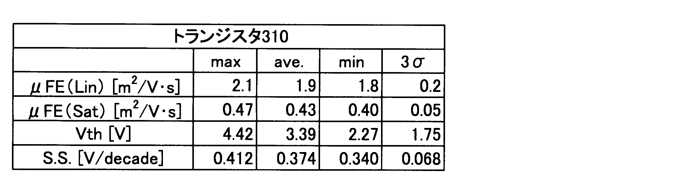
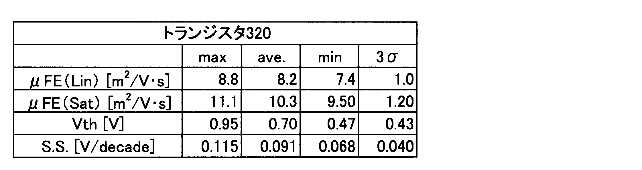
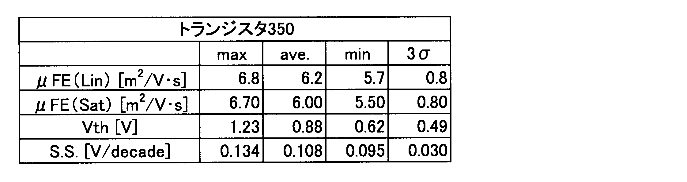
Claims (14)
- 基板と、
発光素子と、
駆動電源線から前記発光素子に流す電流値を制御する第1トランジスタと、
前記発光素子の発光輝度に対応する電圧を前記第1トランジスタの第1ゲート電極に書き込む第2トランジスタと、を含み、
前記第1トランジスタは、
前記基板上に設けられた前記第1ゲート電極と、
前記第1ゲート電極上に設けられた第1絶縁膜と、
前記第1絶縁膜上に設けられ、前記第1ゲート電極と重畳する領域を有する第1酸化物半導体層と、
前記第1酸化物半導体層上に設けられた第2絶縁膜と、
前記第2絶縁膜上に設けられた第1導電層と、を含み、
前記第2トランジスタは、
前記基板上に設けられた前記第1絶縁膜と、
前記第1絶縁膜上に設けられた第2酸化物半導体層と、
前記第1酸化物半導体層及び前記第2酸化物半導体層上に設けられ、前記第1絶縁膜の膜厚よりも小さい膜厚を有する第2絶縁膜と、
前記第2絶縁膜上に設けられ、前記第2酸化物半導体層と重畳する領域を有する第2ゲート電極と、を含み、
前記第1導電層は、前記発光素子と電気的に接続される、表示装置。 - 前記第1絶縁膜の膜厚は、250nm以上500nm以下であり、
前記第2絶縁膜の膜厚は、100nm以上200nm以下である、請求項1に記載の表示装置。 - 前記第2トランジスタは、前記第2絶縁膜上に設けられた第2導電層をさらに有し、
前記第1ゲート電極は、前記第2導電層と電気的に接続される、請求項1に記載の表示装置。 - 前記基板と前記第1絶縁膜との間に、前記第2酸化物半導体層及び前記第2ゲート電極と重畳する第3導電層をさらに有する、請求項1に記載の表示装置。
- 前記駆動電源線と電気的に接続された第3トランジスタをさらに有し、
前記第3トランジスタは、
前記基板上に設けられた前記第1絶縁膜と、
前記第1絶縁膜上に設けられた第3酸化物半導体層と、
前記第3酸化物半導体層上に設けられた前記第2絶縁膜と、
前記第2絶縁膜上に設けられ、前記第3酸化物半導体層と重畳する領域を有する第3ゲート電極と、を含む、請求項1に記載の表示装置。 - 基板と、
発光素子と、
駆動電源線から前記発光素子に流す電流値を制御する第1トランジスタと、
前記発光素子の発光輝度に対応する電圧を前記第1トランジスタの第1ゲート電極に書き込む第2トランジスタと、を含み、
前記第1トランジスタは、
前記基板上に設けられた第1ゲート電極と、
前記第1ゲート電極上に設けられた第1絶縁膜と、
前記第1絶縁膜上に設けられ、前記第1ゲート電極と重畳する領域を有する第1酸化物半導体層と、を含み、
前記第2トランジスタは、
前記基板上に設けられた前記第1絶縁膜と、
前記第1絶縁膜上に設けられた第2酸化物半導体層と、
前記第1酸化物半導体層及び前記第2酸化物半導体層上に設けられ、前記第1絶縁膜の膜厚よりも小さい膜厚を有する第2絶縁膜と、
前記第2絶縁膜上に設けられ、前記第2酸化物半導体層と重畳する領域を有する第2ゲート電極と、を含み、
前記第1酸化物半導体層は、第1チャネル領域と、前記第1チャネル領域を挟んで設けられた低濃度不純物領域と、前記低濃度不純物領域に隣接して設けられた第1高濃度不純物領域とを有し、
前記第2酸化物半導体層は、第2チャネル領域と、前記第2チャネル領域を挟んで設けられた第2高濃度不純物領域とを有する、表示装置。 - 前記低濃度不純物領域は、前記第1ゲート電極と重畳する、請求項6に記載の表示装置。
- 前記第1絶縁膜の膜厚は、250nm以上500nm以下であり、
前記第2絶縁膜の膜厚は、100nm以上200nm以下である、請求項6に記載の表示装置。 - 前記第1高濃度不純物領域に含まれる不純物元素と、前記第2高濃度不純物領域に含まれる不純物元素とは同じ元素である、請求項6に記載の表示装置。
- 前記第1高濃度不純物領域及び前記第2高濃度不純物領域に含まれる不純物元素の濃度は、1×10¹⁵atoms/cm3以上であり、
前記低濃度不純物領域に含まれる不純物元素の濃度は、2.5×10¹²atoms/cm3以上5×1013atoms/cm3未満である、請求項6に記載の表示装置。 - 前記第2トランジスタは、前記第2絶縁膜上に設けられた第1導電層をさらに有し、
前記第1ゲート電極は、前記第1導電層と電気的に接続される、請求項6に記載の表示装置。 - 前記第1酸化物半導体層上に設けられた第2絶縁膜と、
前記第2絶縁膜に設けられた第2導電層と、をさらに有し、
前記第2導電層は、前記発光素子と電気的に接続される、請求項6に記載の表示装置。 - 前記基板と前記第1絶縁膜との間に、前記第2酸化物半導体層及び前記第2ゲート電極と重畳する第3導電層をさらに有する、請求項6に記載の表示装置。
- 前記駆動電源線と電気的に接続された第3トランジスタをさらに有し、
前記第3トランジスタは、
前記基板上に設けられた第4導電層と、
前記第4導電層上に設けられた前記第1絶縁膜と、
前記第1絶縁膜上に設けられ、前記第4導電層と重畳する領域を有する第3酸化物半導体層と、
前記第3酸化物半導体層上に設けられた前記第2絶縁膜と、
前記第2絶縁膜上に設けられ、前記第3酸化物半導体層と重畳する領域を有する第3ゲート電極と、を含む、請求項6に記載の表示装置。
Priority Applications (4)
| Application Number | Priority Date | Filing Date | Title |
|---|---|---|---|
| CN202180057008.XA CN116057610B (zh) | 2020-08-07 | 2021-07-13 | 显示装置 |
| KR1020237003020A KR102954170B1 (ko) | 2020-08-07 | 2021-07-13 | 표시 장치 |
| US18/104,300 US12505796B2 (en) | 2020-08-07 | 2023-02-01 | Display device |
| US19/406,977 US20260087993A1 (en) | 2020-08-07 | 2025-12-03 | Display device |
Applications Claiming Priority (2)
| Application Number | Priority Date | Filing Date | Title |
|---|---|---|---|
| JP2020135399A JP7610936B2 (ja) | 2020-08-07 | 2020-08-07 | 表示装置 |
| JP2020-135399 | 2020-08-07 |
Related Child Applications (1)
| Application Number | Title | Priority Date | Filing Date |
|---|---|---|---|
| US18/104,300 Continuation US12505796B2 (en) | 2020-08-07 | 2023-02-01 | Display device |
Publications (1)
| Publication Number | Publication Date |
|---|---|
| WO2022030199A1 true WO2022030199A1 (ja) | 2022-02-10 |
Family
ID=80118007
Family Applications (1)
| Application Number | Title | Priority Date | Filing Date |
|---|---|---|---|
| PCT/JP2021/026300 Ceased WO2022030199A1 (ja) | 2020-08-07 | 2021-07-13 | 表示装置 |
Country Status (4)
| Country | Link |
|---|---|
| US (2) | US12505796B2 (ja) |
| JP (1) | JP7610936B2 (ja) |
| CN (1) | CN116057610B (ja) |
| WO (1) | WO2022030199A1 (ja) |
Cited By (1)
| Publication number | Priority date | Publication date | Assignee | Title |
|---|---|---|---|---|
| WO2023226082A1 (zh) * | 2022-05-23 | 2023-11-30 | 深圳市华星光电半导体显示技术有限公司 | 像素电路及显示面板 |
Families Citing this family (4)
| Publication number | Priority date | Publication date | Assignee | Title |
|---|---|---|---|---|
| KR20230166546A (ko) * | 2022-05-31 | 2023-12-07 | 엘지디스플레이 주식회사 | 박막 트랜지스터 및 이를 포함하는 표시 장치 |
| US12511463B2 (en) * | 2022-08-31 | 2025-12-30 | Apple Inc. | Backside contacts for signal routing |
| KR20240170614A (ko) * | 2023-05-24 | 2024-12-04 | 삼성디스플레이 주식회사 | 표시 장치 |
| KR20260005442A (ko) * | 2024-07-02 | 2026-01-12 | 삼성디스플레이 주식회사 | 표시 패널 검사 방법 |
Citations (6)
| Publication number | Priority date | Publication date | Assignee | Title |
|---|---|---|---|---|
| WO2015118472A1 (en) * | 2014-02-07 | 2015-08-13 | Semiconductor Energy Laboratory Co., Ltd. | Semiconductor device |
| JP2017017683A (ja) * | 2015-07-02 | 2017-01-19 | 株式会社半導体エネルギー研究所 | 半導体装置および電子機器 |
| US20170098666A1 (en) * | 2015-10-05 | 2017-04-06 | Samsung Display Co., Ltd. | Thin film transistor substrate, display apparatus including thin film transistor substrate, method of manufacturing thin film transistor substrate, and method of manufacturing display apparatus |
| WO2019130915A1 (ja) * | 2017-12-26 | 2019-07-04 | 株式会社ジャパンディスプレイ | 表示装置 |
| JP2020012971A (ja) * | 2018-07-18 | 2020-01-23 | 株式会社ジャパンディスプレイ | 表示装置 |
| JP2020113628A (ja) * | 2019-01-10 | 2020-07-27 | 株式会社ジャパンディスプレイ | 半導体装置及び表示装置 |
Family Cites Families (7)
| Publication number | Priority date | Publication date | Assignee | Title |
|---|---|---|---|---|
| JP2009200528A (ja) * | 2009-06-03 | 2009-09-03 | Sharp Corp | 薄膜トランジスタ装置及びその製造方法 |
| KR20250172710A (ko) | 2012-05-10 | 2025-12-09 | 가부시키가이샤 한도오따이 에네루기 켄큐쇼 | 반도체 장치 |
| US10290573B2 (en) | 2015-07-02 | 2019-05-14 | Semiconductor Energy Laboratory Co., Ltd. | Semiconductor device and electronic device |
| KR102584959B1 (ko) * | 2016-08-31 | 2023-10-06 | 엘지디스플레이 주식회사 | 표시장치 |
| JP2019121696A (ja) * | 2018-01-05 | 2019-07-22 | 株式会社ジャパンディスプレイ | 半導体装置およびその製造方法 |
| US11342362B2 (en) * | 2018-03-30 | 2022-05-24 | Sharp Kabushiki Kaisha | Display device |
| JP2019186273A (ja) * | 2018-04-03 | 2019-10-24 | 株式会社ジャパンディスプレイ | 半導体装置及び表示装置 |
-
2020
- 2020-08-07 JP JP2020135399A patent/JP7610936B2/ja active Active
-
2021
- 2021-07-13 CN CN202180057008.XA patent/CN116057610B/zh active Active
- 2021-07-13 WO PCT/JP2021/026300 patent/WO2022030199A1/ja not_active Ceased
-
2023
- 2023-02-01 US US18/104,300 patent/US12505796B2/en active Active
-
2025
- 2025-12-03 US US19/406,977 patent/US20260087993A1/en active Pending
Patent Citations (6)
| Publication number | Priority date | Publication date | Assignee | Title |
|---|---|---|---|---|
| WO2015118472A1 (en) * | 2014-02-07 | 2015-08-13 | Semiconductor Energy Laboratory Co., Ltd. | Semiconductor device |
| JP2017017683A (ja) * | 2015-07-02 | 2017-01-19 | 株式会社半導体エネルギー研究所 | 半導体装置および電子機器 |
| US20170098666A1 (en) * | 2015-10-05 | 2017-04-06 | Samsung Display Co., Ltd. | Thin film transistor substrate, display apparatus including thin film transistor substrate, method of manufacturing thin film transistor substrate, and method of manufacturing display apparatus |
| WO2019130915A1 (ja) * | 2017-12-26 | 2019-07-04 | 株式会社ジャパンディスプレイ | 表示装置 |
| JP2020012971A (ja) * | 2018-07-18 | 2020-01-23 | 株式会社ジャパンディスプレイ | 表示装置 |
| JP2020113628A (ja) * | 2019-01-10 | 2020-07-27 | 株式会社ジャパンディスプレイ | 半導体装置及び表示装置 |
Cited By (2)
| Publication number | Priority date | Publication date | Assignee | Title |
|---|---|---|---|---|
| WO2023226082A1 (zh) * | 2022-05-23 | 2023-11-30 | 深圳市华星光电半导体显示技术有限公司 | 像素电路及显示面板 |
| US12293710B2 (en) | 2022-05-23 | 2025-05-06 | Shenzhen China Star Optoelectronics Semiconductor Display Technology Co., Ltd. | Pixel circuit and display panel |
Also Published As
| Publication number | Publication date |
|---|---|
| KR20230029910A (ko) | 2023-03-03 |
| JP2022031020A (ja) | 2022-02-18 |
| US20260087993A1 (en) | 2026-03-26 |
| US12505796B2 (en) | 2025-12-23 |
| CN116057610B (zh) | 2025-07-08 |
| JP7610936B2 (ja) | 2025-01-09 |
| CN116057610A (zh) | 2023-05-02 |
| US20230169922A1 (en) | 2023-06-01 |
Similar Documents
| Publication | Publication Date | Title |
|---|---|---|
| US12068335B2 (en) | Light-emitting device | |
| US20230268348A1 (en) | Oxide semiconductor, thin film transistor, and display device | |
| WO2022030199A1 (ja) | 表示装置 | |
| CN118198138A (zh) | 薄膜晶体管及其制造方法以及包括薄膜晶体管的显示装置 | |
| CN102013433B (zh) | 有机发光二极管显示器 | |
| JP2026041807A (ja) | 表示装置 | |
| US20240381693A1 (en) | Display device | |
| CN117637760A (zh) | 包括氧化物半导体图案的薄膜晶体管阵列基板及包括其的显示设备 | |
| JP2025138825A (ja) | 発光装置 | |
| KR102954170B1 (ko) | 표시 장치 | |
| JP2016103605A (ja) | 薄膜トランジスタおよびその製造方法、ならびに表示装置および電子機器 | |
| US20250113709A1 (en) | Display device |
Legal Events
| Date | Code | Title | Description |
|---|---|---|---|
| 121 | Ep: the epo has been informed by wipo that ep was designated in this application |
Ref document number: 21852433 Country of ref document: EP Kind code of ref document: A1 |
|
| ENP | Entry into the national phase |
Ref document number: 20237003020 Country of ref document: KR Kind code of ref document: A |
|
| NENP | Non-entry into the national phase |
Ref country code: DE |
|
| 122 | Ep: pct application non-entry in european phase |
Ref document number: 21852433 Country of ref document: EP Kind code of ref document: A1 |
|
| WWG | Wipo information: grant in national office |
Ref document number: 202180057008.X Country of ref document: CN |