WO2022024932A1 - 配線基板、発光素子搭載用パッケージおよび発光装置 - Google Patents
配線基板、発光素子搭載用パッケージおよび発光装置 Download PDFInfo
- Publication number
- WO2022024932A1 WO2022024932A1 PCT/JP2021/027374 JP2021027374W WO2022024932A1 WO 2022024932 A1 WO2022024932 A1 WO 2022024932A1 JP 2021027374 W JP2021027374 W JP 2021027374W WO 2022024932 A1 WO2022024932 A1 WO 2022024932A1
- Authority
- WO
- WIPO (PCT)
- Prior art keywords
- resin layer
- insulating resin
- wiring board
- ridge line
- closed pore
- Prior art date
Links
- 229920005989 resin Polymers 0.000 claims abstract description 229
- 239000011347 resin Substances 0.000 claims abstract description 229
- 239000011148 porous material Substances 0.000 claims abstract description 187
- 229910052751 metal Inorganic materials 0.000 claims abstract description 91
- 239000002184 metal Substances 0.000 claims abstract description 91
- 239000004020 conductor Substances 0.000 claims abstract description 23
- 239000000758 substrate Substances 0.000 claims description 89
- 239000010954 inorganic particle Substances 0.000 claims description 19
- 238000009826 distribution Methods 0.000 claims description 14
- 239000002245 particle Substances 0.000 claims description 14
- 230000000149 penetrating effect Effects 0.000 claims description 2
- 239000000463 material Substances 0.000 description 14
- 239000000853 adhesive Substances 0.000 description 10
- 230000001070 adhesive effect Effects 0.000 description 10
- 238000004519 manufacturing process Methods 0.000 description 10
- 229920001187 thermosetting polymer Polymers 0.000 description 9
- 230000002093 peripheral effect Effects 0.000 description 8
- 239000003822 epoxy resin Substances 0.000 description 6
- 229920000647 polyepoxide Polymers 0.000 description 6
- VYPSYNLAJGMNEJ-UHFFFAOYSA-N Silicium dioxide Chemical compound O=[Si]=O VYPSYNLAJGMNEJ-UHFFFAOYSA-N 0.000 description 5
- 229910052782 aluminium Inorganic materials 0.000 description 4
- XAGFODPZIPBFFR-UHFFFAOYSA-N aluminium Chemical compound [Al] XAGFODPZIPBFFR-UHFFFAOYSA-N 0.000 description 4
- 238000010438 heat treatment Methods 0.000 description 4
- 238000010191 image analysis Methods 0.000 description 4
- RYGMFSIKBFXOCR-UHFFFAOYSA-N Copper Chemical compound [Cu] RYGMFSIKBFXOCR-UHFFFAOYSA-N 0.000 description 3
- 238000013461 design Methods 0.000 description 3
- 238000011156 evaluation Methods 0.000 description 3
- 238000000034 method Methods 0.000 description 3
- 230000035882 stress Effects 0.000 description 3
- PXHVJJICTQNCMI-UHFFFAOYSA-N Nickel Chemical compound [Ni] PXHVJJICTQNCMI-UHFFFAOYSA-N 0.000 description 2
- 239000000919 ceramic Substances 0.000 description 2
- 239000003795 chemical substances by application Substances 0.000 description 2
- 229910052802 copper Inorganic materials 0.000 description 2
- 239000010949 copper Substances 0.000 description 2
- 238000005336 cracking Methods 0.000 description 2
- 238000010030 laminating Methods 0.000 description 2
- 230000014759 maintenance of location Effects 0.000 description 2
- 238000012545 processing Methods 0.000 description 2
- 239000002994 raw material Substances 0.000 description 2
- 229910000679 solder Inorganic materials 0.000 description 2
- 238000012360 testing method Methods 0.000 description 2
- 230000008646 thermal stress Effects 0.000 description 2
- 229910015363 Au—Sn Inorganic materials 0.000 description 1
- 229910000881 Cu alloy Inorganic materials 0.000 description 1
- 229910052581 Si3N4 Inorganic materials 0.000 description 1
- HCHKCACWOHOZIP-UHFFFAOYSA-N Zinc Chemical compound [Zn] HCHKCACWOHOZIP-UHFFFAOYSA-N 0.000 description 1
- PNEYBMLMFCGWSK-UHFFFAOYSA-N aluminium oxide Inorganic materials [O-2].[O-2].[O-2].[Al+3].[Al+3] PNEYBMLMFCGWSK-UHFFFAOYSA-N 0.000 description 1
- 238000012790 confirmation Methods 0.000 description 1
- 239000011889 copper foil Substances 0.000 description 1
- 238000005520 cutting process Methods 0.000 description 1
- 230000002950 deficient Effects 0.000 description 1
- QGBSISYHAICWAH-UHFFFAOYSA-N dicyandiamide Chemical compound NC(N)=NC#N QGBSISYHAICWAH-UHFFFAOYSA-N 0.000 description 1
- 230000000694 effects Effects 0.000 description 1
- 238000009713 electroplating Methods 0.000 description 1
- 230000017525 heat dissipation Effects 0.000 description 1
- 238000009413 insulation Methods 0.000 description 1
- 239000007788 liquid Substances 0.000 description 1
- 238000005259 measurement Methods 0.000 description 1
- 229910052759 nickel Inorganic materials 0.000 description 1
- 230000035515 penetration Effects 0.000 description 1
- 238000007747 plating Methods 0.000 description 1
- 238000002360 preparation method Methods 0.000 description 1
- 239000004065 semiconductor Substances 0.000 description 1
- 239000000377 silicon dioxide Substances 0.000 description 1
- HQVNEWCFYHHQES-UHFFFAOYSA-N silicon nitride Chemical compound N12[Si]34N5[Si]62N3[Si]51N64 HQVNEWCFYHHQES-UHFFFAOYSA-N 0.000 description 1
- 229910052725 zinc Inorganic materials 0.000 description 1
- 239000011701 zinc Substances 0.000 description 1
Images


Classifications
-
- H—ELECTRICITY
- H01—ELECTRIC ELEMENTS
- H01L—SEMICONDUCTOR DEVICES NOT COVERED BY CLASS H10
- H01L33/00—Semiconductor devices having potential barriers specially adapted for light emission; Processes or apparatus specially adapted for the manufacture or treatment thereof or of parts thereof; Details thereof
- H01L33/48—Semiconductor devices having potential barriers specially adapted for light emission; Processes or apparatus specially adapted for the manufacture or treatment thereof or of parts thereof; Details thereof characterised by the semiconductor body packages
- H01L33/62—Arrangements for conducting electric current to or from the semiconductor body, e.g. lead-frames, wire-bonds or solder balls
-
- H—ELECTRICITY
- H01—ELECTRIC ELEMENTS
- H01L—SEMICONDUCTOR DEVICES NOT COVERED BY CLASS H10
- H01L23/00—Details of semiconductor or other solid state devices
- H01L23/12—Mountings, e.g. non-detachable insulating substrates
-
- H—ELECTRICITY
- H05—ELECTRIC TECHNIQUES NOT OTHERWISE PROVIDED FOR
- H05K—PRINTED CIRCUITS; CASINGS OR CONSTRUCTIONAL DETAILS OF ELECTRIC APPARATUS; MANUFACTURE OF ASSEMBLAGES OF ELECTRICAL COMPONENTS
- H05K1/00—Printed circuits
- H05K1/02—Details
- H05K1/03—Use of materials for the substrate
- H05K1/05—Insulated conductive substrates, e.g. insulated metal substrate
- H05K1/056—Insulated conductive substrates, e.g. insulated metal substrate the metal substrate being covered by an organic insulating layer
-
- H—ELECTRICITY
- H01—ELECTRIC ELEMENTS
- H01L—SEMICONDUCTOR DEVICES NOT COVERED BY CLASS H10
- H01L25/00—Assemblies consisting of a plurality of individual semiconductor or other solid state devices ; Multistep manufacturing processes thereof
- H01L25/03—Assemblies consisting of a plurality of individual semiconductor or other solid state devices ; Multistep manufacturing processes thereof all the devices being of a type provided for in the same subgroup of groups H01L27/00 - H01L33/00, or in a single subclass of H10K, H10N, e.g. assemblies of rectifier diodes
- H01L25/04—Assemblies consisting of a plurality of individual semiconductor or other solid state devices ; Multistep manufacturing processes thereof all the devices being of a type provided for in the same subgroup of groups H01L27/00 - H01L33/00, or in a single subclass of H10K, H10N, e.g. assemblies of rectifier diodes the devices not having separate containers
- H01L25/075—Assemblies consisting of a plurality of individual semiconductor or other solid state devices ; Multistep manufacturing processes thereof all the devices being of a type provided for in the same subgroup of groups H01L27/00 - H01L33/00, or in a single subclass of H10K, H10N, e.g. assemblies of rectifier diodes the devices not having separate containers the devices being of a type provided for in group H01L33/00
- H01L25/0753—Assemblies consisting of a plurality of individual semiconductor or other solid state devices ; Multistep manufacturing processes thereof all the devices being of a type provided for in the same subgroup of groups H01L27/00 - H01L33/00, or in a single subclass of H10K, H10N, e.g. assemblies of rectifier diodes the devices not having separate containers the devices being of a type provided for in group H01L33/00 the devices being arranged next to each other
-
- H—ELECTRICITY
- H01—ELECTRIC ELEMENTS
- H01L—SEMICONDUCTOR DEVICES NOT COVERED BY CLASS H10
- H01L33/00—Semiconductor devices having potential barriers specially adapted for light emission; Processes or apparatus specially adapted for the manufacture or treatment thereof or of parts thereof; Details thereof
- H01L33/48—Semiconductor devices having potential barriers specially adapted for light emission; Processes or apparatus specially adapted for the manufacture or treatment thereof or of parts thereof; Details thereof characterised by the semiconductor body packages
- H01L33/483—Containers
- H01L33/486—Containers adapted for surface mounting
-
- H—ELECTRICITY
- H01—ELECTRIC ELEMENTS
- H01L—SEMICONDUCTOR DEVICES NOT COVERED BY CLASS H10
- H01L33/00—Semiconductor devices having potential barriers specially adapted for light emission; Processes or apparatus specially adapted for the manufacture or treatment thereof or of parts thereof; Details thereof
- H01L33/48—Semiconductor devices having potential barriers specially adapted for light emission; Processes or apparatus specially adapted for the manufacture or treatment thereof or of parts thereof; Details thereof characterised by the semiconductor body packages
- H01L33/64—Heat extraction or cooling elements
- H01L33/641—Heat extraction or cooling elements characterized by the materials
Definitions
- This disclosure relates to a wiring board, a package for mounting a light emitting element, and a light emitting device.
- LEDs Light Emitting Diodes
- LDs Laser Diodes
- a light source device using these semiconductor elements is required to have high heat dissipation. Therefore, a metal substrate is used for the light source device.
- An insulating layer made of an organic resin is laminated on the metal substrate to form a wiring board or a package for mounting a light emitting element (see, for example, Patent Document 1).
- the wiring board of the present disclosure has a metal substrate, an insulating resin layer located on the metal substrate, and a conductor layer located on the insulating resin layer.
- the insulating resin layer includes a first surface facing the metal substrate, a second surface located opposite to the first surface, and a third surface located between the first surface and the second surface. It includes a first ridge line portion where the first surface and the third surface intersect, and a second ridge line portion where the second surface and the third surface intersect.
- the insulating resin layer has a first closed pore group in which a plurality of closed pores are densely packed closer to the first ridge line portion than to the second ridge line portion.
- the wiring board of the present disclosure has a metal substrate, an insulating resin layer located on the metal substrate, and a conductor layer located on the insulating resin layer.
- the insulating resin layer includes a first surface facing the metal substrate, a second surface located opposite to the first surface, a through hole penetrating the first surface to the second surface, and the inside of the through hole.
- the fourth surface located between the first surface and the second surface, the third ridge line portion where the first surface and the fourth surface intersect, and the second surface and the fourth ridge line portion. I have.
- the insulating resin layer has a second closed pore group in which a plurality of closed pores are densely packed closer to the third ridge line portion than to the fourth ridge line portion.
- a submount for mounting the light emitting element is arranged on the above wiring board.
- the light emitting device of the present disclosure includes a light emitting element on a submount of the above-mentioned light emitting element mounting package.
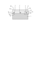
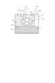
- FIG. 1 is an external perspective view of a wiring board shown as an example of an embodiment.
- FIG. 2 is a sectional view taken along line II-II of FIG.
- FIG. 3 is a cross-sectional view taken along the line III-III of FIG.
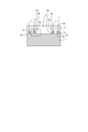
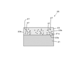
- FIG. 4 is an enlarged cross-sectional view of the P1 portion of FIG.
- FIG. 5 is an external perspective view showing another aspect of the wiring board.
- FIG. 6 is a sectional view taken along line VI-VI of FIG.
- FIG. 7 is a sectional view taken along line VII-VII of FIG.
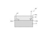
- FIG. 8 is an enlarged cross-sectional view of the P2 portion of FIG.
- FIG. 9 is a schematic cross-sectional view of a light emitting device shown as an example of the embodiment.
- FIG. 1 is an external perspective view of a wiring board shown as an example of an embodiment.
- FIG. 2 is a sectional view taken along line II-II of FIG.
- FIG. 3 is a cross-sectional view
- FIG. 10A is a cross-sectional view showing a part of the manufacturing process of the wiring board A and a state before the laminated body is pressure-heated.
- FIG. 10B is a cross-sectional view showing a part of the manufacturing process of the wiring board A and a state after the laminated body is pressure-heated.
- FIG. 11A is a cross-sectional view showing a part of the manufacturing process of the wiring board B and showing a state before the laminated body is pressure-heated.
- FIG. 11B is a cross-sectional view showing a part of the manufacturing process of the wiring board B and showing a state after the laminated body is pressure-heated.
- the light emitting element mounting package disclosed in Patent Document 1 has a structure in which an insulating layer made of an organic resin is laminated on a metal substrate.
- a metal substrate may be referred to as a substrate.
- An insulating layer made of an organic resin may be referred to as an insulating layer.
- the substrate and the insulating layer are made of different materials. Therefore, it is basically difficult to firmly bond the substrate and the insulating layer.
- the package for mounting a light emitting element is exposed to a sudden temperature change, there may be a problem that the insulating layer is peeled off from the substrate. This is because the substrate and the insulating layer have a large difference in thermal expansion coefficient between them.
- the insulating layer has high rigidity even if it is made of an organic resin.
- the Young's modulus of the insulating layer made of an organic resin increases sharply, especially when the ambient temperature is lower than the normal temperature (25 ° C.). Due to such factors, the insulating layer of a light emitting device mounting package having a structure in which an insulating layer made of an organic resin is laminated on a metal substrate is easily peeled off from the substrate.
- the present disclosure provides, for example, a wiring board, a package for mounting a light emitting element, and a light emitting device in which the insulating layer is not easily peeled off from the substrate even in a structure in which an insulating layer made of an organic resin is laminated on a metal substrate.
- FIG. 1 is an external perspective view of a wiring board shown as an example of an embodiment.
- FIG. 2 is a sectional view taken along line II-II of FIG.
- FIG. 3 is a cross-sectional view taken along the line III-III of FIG.
- FIG. 4 is an enlarged cross-sectional view of the P1 portion of FIG.
- the wiring board A shown in FIG. 1 has a metal substrate 1, an insulating resin layer 3, and a conductor layer 5.
- the insulating resin layer 3 is located on the metal substrate 1.
- the insulating resin layer 3 is laminated on the metal substrate 1.
- the conductor layer 5 is located on the insulating resin layer 3.
- the conductor layer 5 is arranged toward the end of the second surface 3b of the insulating resin layer 3, but the position of the conductor layer 5 is not limited to this.
- the conductor layer 5 may be arranged at any place required by the pattern design. Further, in FIG. 1, the number of the conductor layers 5 is two, but the number of the conductor layers 5 may be arranged as many as necessary.
- the insulating resin layer 3 has a first surface 3a, a second surface 3b, and a third surface 3c.
- the first surface 3a is a surface facing the metal substrate 1.
- the second surface 3b is a surface located on the opposite side of the first surface 3a.
- the third surface 3c is a surface located between the first surface 3a and the second surface 3b.
- the first surface 3a and the second surface 3b are the main surfaces of the insulating resin layer 3.
- the third surface 3c is a so-called side surface of the insulating resin layer 3.
- the third surface 3c is oriented so as to intersect the first surface 3a or the second surface 3b.
- the third surface 3c has a structure that faces in a direction perpendicular to the first surface 3a and the second surface 3b, but is not limited to the direction perpendicular to the first surface 3a and the second surface 3b.
- the wiring board A shown in FIG. 1 has four third surfaces 3c.
- the insulating resin layer 3 has a first ridge line portion 3d and a second ridge line portion 3e.
- the first ridge line portion 3d is located at a position where the first surface 3a and the third surface 3c intersect.
- the second ridge line portion 3e is located at the intersection of the second surface 3b and the third surface 3c.
- the first ridge line portion 3d is a ridge line closer to the metal substrate 1 than the second ridge line portion 3e.
- the first ridge line portion 3d is arranged so as to surround the first surface 3a of the insulating resin layer 3.
- the second ridge line portion 3e is arranged so as to surround the second surface 3b of the insulating resin layer 3.
- the insulating resin layer 3 has a large number of closed pores 7a.
- the insulating resin layer 3 among a large number of closed pores 7a, there is a portion in which a plurality of closed pores are densely packed.
- the portion in which a plurality of closed pores 7a are densely packed is hereinafter referred to as a closed pore group.
- the closed pore group existing in the insulating resin layer 3 of the wiring board A is referred to as the first closed pore group 7.
- the state in which a plurality of closed pores 7a are densely referred to means a state in which the number of closed pores 7a existing in a predetermined volume is larger than that in other regions.
- the volume may be replaced with a predetermined area (unit area) of the cross section of the insulating resin layer 3.
- the unit area can be drawn by monotonically connecting the contours of the plurality of closed pores 7a located on the outermost periphery in the portion where the plurality of closed pores are densely packed.
- the area of the circle In this case, the porosity of the first closed pore group 7 is preferably 50% or more of the porosity in the unit area. As a guide, the porosity of the first closed pore group is up to 80%.
- the first closed pore group 7 exists closer to the first ridge line portion 3d than the second ridge line portion 3e of the insulating resin layer 3. In other words, the first closed pore group 7 exists in the vicinity of the first ridge line portion 3d in the insulating resin layer 3. Furthermore, the first closed pore group 7 exists in the insulating resin layer 3 near the outer peripheral edge of the first surface 3a.
- the proportion of the resin forming the insulating resin layer 3 is smaller than in the other regions of the insulating resin layer 3. Therefore, in the insulating resin layer 3, the region where the first closed pore group 7 exists has a lower elastic modulus than the other regions of the insulating resin layer 3.
- a portion having a lower elastic modulus than other regions is formed in the vicinity of the first ridge line portion 3d of the insulating resin layer 3. As a result, the stress generated between the metal substrate 1 and the insulating resin layer 3 can be relaxed. As a result, the probability that the metal substrate 1 and the insulating resin layer 3 are separated from each other can be reduced.
- the possibility that the insulating resin layer 3 will be peeled off from the metal substrate 1 can be reduced.
- the thermal expansion rate is different between the metal substrate 1 and the insulating resin layer 3, the insulating resin layer 3 is easily peeled off from the peripheral edge 3co.
- the insulating resin layer 3 tends to be easily peeled off from the corner portion 3 coc.
- the first closed pore group 7 exists in the vicinity of the first ridge line portion 3d in the insulating resin layer 3. Therefore, it is possible to prevent the insulating resin layer 3 from peeling off from the corner portion 3coc and the peripheral edge 3co.
- the elastic modulus of the portion where the first closed pore group 7 exists has a low elastic modulus.
- the portion where the first closed pore group 7 exists is easily deformed. Therefore, the adhesive force of the metal substrate 1 to the surface 1a is increased.
- the portion where the first closed pore group 7 exists is close to the surface 1a of the metal substrate 1 in the direction of the thickness of the insulating resin layer 3 and is close to the surface 1a of the metal substrate 1.
- the insulating resin layer 3 is viewed in a plan view, it is a portion close to the peripheral edge 3co of the insulating resin layer 3.
- the other region is from the surface 1a of the metal substrate 1 in the direction of the thickness of the insulating resin layer 3 rather than the place where the first closed pore group 7 exists. It is a distant place, and when the insulating resin layer 3 is viewed in a plan view, it is located closer to the center 3cc than the peripheral edge 3co of the insulating resin layer 3.
- the first closed pore group 7 includes a plurality of closed pores 7a.
- the closed pores 7a are pores existing inside the insulating resin layer 3.
- the closed pore 7a has a closed space.
- the closed pores 7a do not face the first surface 3a, the second surface 3b, the side surface (third surface 3c), and the first ridge line portion 3d of the insulating resin layer 3.
- the closed pores 7a have a resin between the first surface 3a, the second surface 3b, the side surface (third surface 3c), and the first ridge line portion 3d constituting the insulating resin layer 3.
- the closed pore 7a does not have a portion opened in the first surface 3a, the second surface 3b, the side surface (third surface 3c), and the first ridge line portion 3d of the insulating resin layer 3.
- the closed pores 7a are present alone in other regions of the portion that is the first closed pore group 7.
- the closed pores 7a constituting the first closed pore group 7 have a larger average diameter than the closed pores 7a existing in a region other than the portion of the first closed pore group 7.
- the average diameter D1 of the closed pores 7a constituting the first closed pore group 7 is 1.5 to 1.5 of the average diameter D2 of the closed pores 7a existing in the region other than the portion of the first closed pore group 7. It may be 5 times.
- Confirmation of the region from the large number of closed pores 7a included in the insulating resin layer 3 to the first closed pore group 7 is performed as follows. First, a cross section as shown in FIG. 3 is extracted from the wiring board A. Next, the cross section is observed with an electron microscope, for example, and the presence of the closed pores 7a is confirmed from the photograph. Next, a candidate for the first closed pore group 7, which is a portion where the closed pores 7a are densely packed, is searched for, and a provisional division is performed visually with the region where the closed pores 7a are not densely packed.
- the diameter of each closed pore 7a is obtained by image analysis of the candidate portion of the first closed pore group 7.
- the diameter of each closed pore 7a is obtained by converting the area of the closed pore 7a obtained from the image analysis into the area of a circle.
- the range from the measured value of the diameter of each of the obtained closed pores 7a to the range in which the closed pores 7a larger than the threshold diameter are present is defined as the range of the first closed pore group 7.
- the threshold value of the diameter of the closed pore 7a is 0.05 ⁇ m in the specific example described later. If the closed pores having a diameter smaller than 0.05 ⁇ m exist between the closed pores 7a constituting the first closed pore group 7, the closed pores 7a having such a small diameter are also the first.
- thermosetting resin is suitable as the material of the insulating resin layer 3.
- Epoxy resin is suitable as the thermosetting resin.
- Inorganic particles may be contained in the insulating resin layer 3.
- Copper foil is suitable as the conductor layer 5.
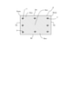
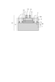
- FIG. 5 is an external perspective view showing another aspect of the wiring board.
- FIG. 6 is a sectional view taken along line VI-VI of FIG.
- FIG. 7 is a sectional view taken along line VII-VII of FIG.
- FIG. 8 is an enlarged cross-sectional view of the P2 portion of FIG.
- the wiring board B shown in FIG. 5 has a metal substrate 1, an insulating resin layer 3, and a conductor layer 5.
- the insulating resin layer 3 is located on the metal substrate 1.
- the conductor layer 5 is located on the insulating resin layer 3.
- the conductor layer 5 is arranged toward the end of the second surface 3b of the insulating resin layer 3, but the position of the conductor layer 5 is not limited to this. It is arranged in the required place by the pattern design of the conductor layer 5.
- the number of the conductor layers 5 is 2, but the number of the conductor layers 5 may be the number required by the pattern design.
- the insulating resin layer 3 has a first surface 3a and a second surface 3b.
- the insulating resin layer 3 has a through hole 9.
- the wiring board B shown in FIG. 5 is different from the wiring board A described above in that the insulating resin layer 3 has a through hole 9.
- the through hole 9 is formed so as to penetrate between the first surface 3a and the second surface 3b of the insulating resin layer 3.
- the through hole 9 has an inner surface 9a.
- the inner surface 9a is located between the first surface 3a and the second surface 3b of the insulating resin layer 3.
- the through hole 9 shown in FIG. 5 has a rectangular shape in a plan view.
- the inner surface 9a of the through hole 9 is composed of four surfaces.
- one of the inner surfaces 9a of the through hole 9 is referred to as the fourth surface 9aa.
- the inner surface 9a of the through hole 9 shown in FIG. 5 has four fourth surfaces 9aa.
- the fourth surface 9aa is oriented so as to intersect with the first surface 3a.
- the fourth surface 9aa which is one of the four fourth surfaces 9aa, will be described.
- the fourth surface 9aa is located between the first surface 3a and the second surface 3b of the insulating resin layer 3.
- the insulating resin layer 3 has a third ridge line portion 9b and a fourth ridge line portion 9c.
- the third ridge line portion 9b is a portion where the first surface 3a and the fourth surface 9aa of the insulating resin layer 3 intersect.
- the fourth ridge line portion 9c is a portion where the second surface 3b and the fourth surface 9aa of the insulating resin layer 3 intersect.
- the insulating resin layer 3 constituting the wiring board B also has a large number of closed pores as in the case of the wiring board A.
- the insulating resin layer 3 constituting the wiring board B also has a group of closed pores having the same form as that of the wiring board A.
- the closed pore group existing near the through hole 9 formed in the insulating resin layer 3 is referred to as the second closed pore group 11.
- the closed pores constituting the second closed pore group 11 are hereinafter represented by reference numerals 11a.
- the first closed pore group 7 and the closed pore group 7a, the second closed pore group 11 and the closed pore 11a are represented by different reference numerals for convenience of explanation.
- the first closed pore group 7 and the closed pore group 7a and the second closed pore group 11 and the closed pore 11a may have the same size and distribution state, respectively.
- the second closed pore group 11 exists closer to the third ridge line portion 9b than the fourth ridge line portion 9c of the insulating resin layer 3. In other words, the second closed pore group 11 exists in the vicinity of the third ridge line portion 9b in the insulating resin layer 3. In the region where the second closed pore group 11 exists, the proportion of the resin forming the insulating resin layer 3 is smaller than that in the other regions of the insulating resin layer 3.
- the region where the second closed pore group 11 exists has a lower elastic modulus than the other regions of the insulating resin layer 3.
- a portion having a lower elastic modulus than other regions is formed in the vicinity of the third ridge line portion 9b of the insulating resin layer 3.
- the probability that the through hole 9 side of the insulating resin layer 3 is separated from the metal substrate 1 can be reduced.
- the possibility that the through hole 9 side of the insulating resin layer 3 is peeled off from the metal substrate 1 can be reduced.
- the thermal expansion rate is different between the metal substrate 1 and the insulating resin layer 3
- the inner surface 9a of the through hole 9 which is the end surface of the insulating resin layer 3 is likely to be partially peeled off like the peripheral edge 3co.
- the second closed pore group 11 exists in the insulating resin layer 3 near the third ridge line portion 9b. Therefore, the insulating resin layer 3 can be prevented from peeling off from the inner surface 9a side of the through hole 9.
- the elastic modulus of the portion where the second closed pore group 11 exists has a low elastic modulus. Further, the portion where the second closed pore group 11 exists is easily deformed. Therefore, the adhesive force of the metal substrate 1 to the surface 1a is increased.
- the portion where the second closed pore group 11 exists is close to the surface 1a of the metal substrate 1 in the direction of the thickness of the insulating resin layer 3 and is close to the surface 1a.
- the insulating resin layer 3 is viewed in a plan view, it is a portion close to the inner surface 9a of the through hole 9.
- the other region is from the surface 1a of the metal substrate 1 in the direction of the thickness of the insulating resin layer 3 rather than the place where the second closed pore group 11 exists. It is a distant place, and when the insulating resin layer 3 is viewed in a plan view, it is a position close to the peripheral edge 3co from the inner surface 9a of the through hole 9.
- the second closed pore group 11 includes a plurality of closed pores 11a.
- the closed pores 11a are pores existing inside the insulating resin layer 3.
- the closed pore 11a has a closed space.
- the closed pores 11a are the first surface 3a, the second surface 3b, the fourth surface 9aa, the side surface (third surface 3c), the first ridge line portion 3d, the second ridge line portion 3e, and the third ridge line portion 9b of the insulating resin layer 3. It does not face the surface and has a resin between each of these parts and the outside world.
- the closed pores 11a are the first surface 3a, the second surface 3b, the fourth surface 9aa, the side surface (third surface 3c), the first ridge line portion 3d, the second ridge line portion 3e, and the third surface of the insulating resin layer 3. It does not have an opening in the ridgeline portion 9b.
- the closed pores 11a independently exist in the insulating resin layer 3 in a region different from the portion forming the second closed pore group 11.
- the closed pores 11a constituting the second closed pore group 11 have a larger average diameter than the closed pores 11a existing in a region other than the portion of the second closed pore group 11.
- the average diameter D3 of the closed pores 11a constituting the second closed pore group 11 is 1.5 to 1.5 of the average diameter D4 of the closed pores 11a existing in the region other than the portion of the second closed pore group 11. It may be 5 times.
- the wiring board B may have the first closed pore group 7 in the insulating resin layer 3.
- the wiring board B may have a first closed pore group 7 and a second closed pore group 11 in the insulating resin layer 3. That is, the insulating resin layer 3 constituting the wiring board B may have a first closed pore group 7 in which a plurality of closed pores 7a are densely packed near the first ridge line portion 3d.
- the through hole 9 is provided. It is possible to prevent the insulating resin layer 3 laminated on the metal substrate 1 from peeling off from the peripheral edge 3co and the corner portion 3coc as well as the inner surface 9a side.
- the first closed pore group 7 may be located in the entire area extending over the first ridge line portion 3d.
- the insulating resin layer 3 is less likely to be peeled off from the metal substrate 1 in the entire area.
- the second closed pore group 11 may be located in the entire area extending over the third ridge line portion 9b.
- the fact that the first closed pore group 7 is located in the entire area means that the first closed pore group 7 has the maximum length when the maximum length L of the first closed pore group 7 is 1. It means that they are arranged along the first ridge line portion 3d at a pitch of 10 times or less of L. The same applies when the second closed pore group 11 is arranged along the third ridge line portion 9b.
- the insulating resin layer 3 may contain a plurality of inorganic particles, but in this case, it is preferable that the plurality of inorganic particles have two peaks in their particle size distribution.
- the particle size distribution of the inorganic particles contained in the insulating resin layer 3 has two peaks, a structure is formed in which the inorganic particles having a small diameter enter between the large diameter inorganic particles contained in the insulating resin layer 3. can. Therefore, in the insulating resin layer 3, it is possible to obtain the insulating resin layer 3 showing high strength even if the volume ratio of the inorganic particles is low.
- the insulating resin layer 3 can increase the adhesive strength with respect to the metal substrate 1.
- the volume ratio of the inorganic particles is low because the volume ratio of the voids is originally high. Therefore, the effect of stress relaxation due to the presence of the first closed pore group 7 and the second closed pore group 11 in the insulating resin layer 3 can be maintained.
- the particle size distribution of the inorganic particles has two peaks, as long as the particle size distribution of the inorganic particles can be measured and the distribution can be graphed.
- the skirt extending from the peak having the smaller particle size and the skirt extending from the peak having the larger particle size may overlap.
- FIG. 9 is a schematic cross-sectional view of the light emitting device D shown as an example of the embodiment.
- the light emitting device D shown in FIG. 9 has a light emitting element mounting package C and a light emitting element 13.
- a light emitting element 13 As the light emitting element 13, an LD (Laser Diode) can be exemplified in addition to the LED element.
- LD Laser Diode
- the light emitting element mounting package C shown in FIG. 9 is based on the wiring board B shown in FIG.
- the light emitting element mounting package C has a wiring board B, a submount board 15, and a bonding material 17.
- the submount substrate 15 is fitted into a through hole 9 formed in the insulating resin layer 3 constituting the wiring board B.
- the submount substrate 15 is arranged on the metal substrate 1 constituting the wiring board B.
- the bonding material 17 is arranged on the metal substrate 1 in the through hole 9 formed in the insulating resin layer 3 constituting the wiring board B.
- the joining material 17 joins the metal substrate 1 and the submount substrate 15.
- the submount substrate 15 is preferably equipped with a light emitting element 13 that easily generates heat during operation, and thus has the properties of high thermal conductivity, high strength, high toughness, and low thermal expansion. From the viewpoint of having such characteristics, it is preferable to use ceramics for the submount substrate 15. For example, ceramics containing silicon nitride as a main component are preferable. As the bonding material 17, solder, Au-Sn, or the like is preferable. The submount substrate 15, the metal substrate 1, and the insulating resin layer 3 may have different thermal expansion rates.
- the light emitting element mounting package C When the light emitting element 13 is mounted on the light emitting element mounting package C and the light emitting element 13 operates continuously or discontinuously, the light emitting element mounting package C generates heat due to the operation of the light emitting element 13. Thermal stress is generated between the metal substrate 1 bonded to each other and the insulating resin layer 3 due to the difference in the thermal expansion coefficient and Young's modulus of the two. In the case of the light emitting device D, since the second closed pore group 11 exists in the insulating resin layer 3 of the wiring board B constituting the light emitting element mounting package C as described above, the metal substrate 1 and the insulating resin layer are present.
- the submount board 15 is arranged on the second surface 3b of the insulating resin layer 3 of the wiring board A.
- the submount substrate 15 is arranged on the second surface 3b of the insulating resin layer 3 via the bonding material 17.
- FIG. 10A is a cross-sectional view showing a state before the laminated body is pressure-heated.
- FIG. 10B is a cross-sectional view showing a state after the laminated body is pressure-heated.
- the metal plate 21 is a material for obtaining the metal substrate 1.
- the organic resin sheet 23 is a material for obtaining the insulating resin layer 3.
- the metal plate 21 and the organic resin sheet 23 are each processed into a predetermined shape. It is better to use a mechanical cutting machine such as dicing for processing the metal plate.
- a thermosetting resin as the material of the organic resin sheet 23. Epoxy resin is preferable as the material of the thermosetting resin.
- a curing agent may be added to the thermosetting resin.
- the organic resin sheet 23 may contain inorganic particles. As the inorganic particles, silica, alumina and the like are preferable. In this case, the inorganic particles preferably have two peaks when the particle size distribution is measured.
- the organic resin sheet 23 is adhered to the surface 21a of the metal plate 21 to prepare the laminated body 25.
- a laminating machine capable of pressurizing in a heated state is used for the adhesion between the metal plate 21 and the organic resin sheet 23.
- the thermosetting resin used is cured at a temperature higher than the temperature at which the thermosetting resin can be cured.
- the epoxy resin is cured at about 200 ° C.
- the curing temperature is set to a higher temperature of 10 ° C. or higher and 60 ° C. or lower.
- the surface of the insulating resin layer 3 tends to be flattened by dissolving a part of the resin component during pressurization and heating. At this time, the temperature is maintained at the maximum temperature for a predetermined time. When the laminate 25 is produced under such conditions, the bubbles 27 contained inside the organic resin sheet 23 are released from the organic resin sheet 23.
- the bubbles 27 are easily removed from the surface of the organic resin sheet 23 that is not in contact with the metal plate 21, but the bubbles 27 are difficult to be removed from the surface 23a facing the metal plate 21. This is because the surface 23a of the organic resin sheet 23 is in contact with the metal plate 21, so that the bubbles 27 that should be released from the organic resin sheet 23 are blocked by the metal plate 21. Therefore, the bubbles 27 tend to accumulate in the vicinity of the surface 23a of the organic resin sheet 23 facing the metal plate 21.
- the bubbles 27 dispersed in the organic resin sheet 23 are concentrated in the vicinity of the surface 23a facing the metal plate 21. In this way, the ratio of open pores can be reduced from the surface of the insulating resin layer 3.
- a film sheet having holes is placed on the surface of the organic resin sheet 23 opposite to the metal plate 21 so that air bubbles can easily escape.
- the bubbles 27 originally contained in the organic resin sheet 23 are not in contact with the metal plate 21 at the first stage of the pressure heat treatment, and the organic resin sheet 23 is formed. Move towards the part that is released inside.
- the open portion of the organic resin sheet 23 is, for example, the side surface 23b of the organic resin sheet 23.
- the insulating resin layer 3 formed by curing the organic resin sheet 23 is formed with the first closed pore group 7 in which a plurality of closed pores are densely packed.
- the first closed pore group 7 is formed in a region close to the side surface (third surface 3c) of the insulating resin layer 3 and close to the metal plate 21.
- the organic resin sheet 23 since the organic resin sheet 23 has a simple plate shape, the bubbles 27 contained in the organic resin sheet 23 gather in a region close to the side surface 23b of the organic resin sheet 23. In this way, it is possible to obtain a wiring board A having a first closed pore group 7 in which a plurality of closed pores 7a are densely packed closer to the first ridge line portion 3d than the second ridge line portion 3e of the insulating resin layer 3.
- the holding time is short, some of the resin components will not dissolve and the surface will not be flat. Further, when the curing temperature is set to around the above-mentioned normal temperature (for example, 200 ° C.), the surface of the insulating resin layer 3 tends to have an uneven shape, and open pores are likely to be formed. This is because the resin component is difficult to dissolve during pressurization and heating.
- FIG. 11A and 11B show a part of the manufacturing process of the wiring board B.
- FIG. 11A is a cross-sectional view showing a state before the laminated body is pressure-heated.
- FIG. 11B is a cross-sectional view showing a state after the laminated body is pressure-heated.
- the organic resin sheet 23 forms a hole 29 which later becomes a through hole 9 of the insulating resin layer 3.
- a laser processing machine is used in addition to the mold to form the holes 29.
- the bubbles 27 also collect in the region close to the inner surface 29a of the holes 29. As shown in FIG.
- the bubbles 27 gather in both the region near the side surface 23b of the organic resin sheet 23 and the region near the inner surface 29a of the hole 29.
- a plurality of through holes 9 formed in the insulating resin layer 3 are located near the third ridge line portion 9b located closer to the metal substrate 1 than the fourth ridge line portion 9c located on the side farther from the metal substrate 1. It is possible to obtain a wiring board B having a second closed pore group 11 in which closed pores are densely packed.
- the first closed pore group 7 is also formed.
- a film sheet having holes is placed on the surface of the organic resin sheet 23 opposite to the metal plate 21 so that air bubbles can easily escape.
- the organic resin sheet 23 uses inorganic particles having two peaks when the particle size distribution is measured, the organic resin sheet 23 is formed. Since the mechanical strength of the insulating resin layer 3 can be increased, the adhesive strength of the insulating resin layer 3 to the metal substrate 1 can be improved.
- the bonding material 17 is arranged in the through hole 9 of the produced wiring board B.
- the submount substrate 15 is placed on the upper surface of the bonding material 17 and heat-treated.
- the light emitting element 13 is mounted on the surface of the submount substrate 15.
- the light emitting element 13 is electrically connected to the conductor layer 5 provided on the second surface 3b of the insulating resin layer 3 constituting the wiring board B by a bonding wire. In this way, the light emitting device D can be obtained.
- a wiring board was manufactured and its reliability was evaluated.
- a wiring board B was manufactured as a wiring board.
- Aluminum was used for the metal substrate.
- the organic resin sheet to be the insulating resin layer was prepared by mixing an epoxy resin and silica particles. The content of silica particles was 30% by volume. Two types of silica particles were used: a raw material having two peaks in the particle size distribution and a raw material having only one peak in the particle size distribution. Further, 1 part by mass of a curing agent (dicyandiamide) was added to 100 parts by mass of the epoxy resin.
- the through hole of the insulating resin layer was formed by using a mold.
- the conductor layer was formed by an electrolytic plating method using a nickel plating solution containing zinc.
- Table 1 shows the conditions for pressurization and heating when producing the laminate.
- a film sheet with holes was placed on the surface of the insulating resin layer opposite to the metal substrate.
- the manufactured wiring board had the following sizes.
- the area of the plane of the metal substrate and the insulating resin layer is 40 mm ⁇ 40 mm
- the area of the through holes provided in the insulating resin layer is 20 mm ⁇ 20 mm
- the thickness of the metal substrate is 2 mm
- the thickness of the insulating resin layer is 0. It is .2 mm.
- the following evaluation was performed on the prepared sample.
- the evaluation items are the presence or absence of the first closed pore group and the second closed pore group formed in the insulating resin layer, the presence or absence of peeling of the insulating resin layer from the metal substrate, the presence or absence of cracks generated in the insulating resin layer, and the presence or absence of the metal substrate.
- the adhesive strength of the insulating resin layer was defined.
- the presence or absence of the first closed pore group and the second closed pore group formed on the insulating resin layer was determined as follows. First, a cross section as shown in FIG. 3 was extracted from the produced wiring board. Next, the cross section was observed using, for example, a scanning electron microscope, and the presence of closed pores was confirmed from the photograph. Next, candidates for the first closed pore group and the second closed pore group, which are the portions where the closed pores are dense, were searched for, and provisional classification was performed visually with the region where the closed pores were not dense. Next, the diameters of the closed pores were determined by image analysis of the candidate portions of the first closed pore group and the second closed pore group.
- the diameter of each closed pore was obtained by converting the area of the closed pore obtained from the image analysis into the area of a circle.
- the range from the measured value of the diameter of each of the obtained closed pores to the range in which the closed pores larger than the threshold diameter exist was defined as the range of the first closed pore group and the second closed pore group.
- the threshold value of the diameter of the closed pores was set to 0.05 ⁇ m. If the closed pores having a diameter smaller than 0.05 ⁇ m exist between the closed pores constituting the first closed pore group and the second closed pore group, the closed pores having the smaller diameter are also present. It was included in the area of the first closed pore group and the second closed pore group.
- the closed pores having a diameter of 0.01 ⁇ m or less were not measured and were excluded from the measurement target.
- the second closed pore group was formed in the insulating resin layer closer to the third ridge line portion than to the fourth ridge line portion. Further, it was confirmed that the second closed pore group was formed over the entire circumference of the inner wall (inner surface) formed by the four surfaces (fourth surface) constituting the through hole.
- the porosity of the first closed pore group and the second closed pore group was 50% or more. In this case, the porosity of the first closed pore group and the second closed pore group was 70% at the maximum.
- the presence or absence of peeling of the insulating resin layer from the metal substrate was evaluated using a method of immersing the insulating resin layer in a solder bath set at 300 ° C. for 30 seconds.
- the presence or absence of cracks generated in the insulating resin layer was confirmed after the temperature cycle test.
- the conditions of the temperature cycle test are: minimum temperature -55 ° C, maximum temperature 150 ° C, minimum temperature retention time, maximum temperature retention time, and temperature change from minimum temperature to maximum temperature and vice versa. The time for each was set to 15 minutes. The number of temperature cycles was set to 3000.
- the state of peeling and cracking in the insulating resin layer was confirmed by the method of immersing in the red check solution. A sample in which the red check solution was found to have penetrated into the insulating resin layer was judged to be defective. At the same time, the penetration of the red check liquid between the metal substrate and the insulating resin layer was also evaluated.
- the adhesive strength of the insulating resin layer to the metal substrate was measured using a tensile tester (autograph). In all of these evaluations, the number of samples was 10. In this case, the sample in which peeling or cracking was observed even in one of the evaluated samples (10) was described as “presence”. The average value was calculated for the adhesive strength.
Landscapes
- Engineering & Computer Science (AREA)
- Microelectronics & Electronic Packaging (AREA)
- Power Engineering (AREA)
- Computer Hardware Design (AREA)
- Manufacturing & Machinery (AREA)
- Physics & Mathematics (AREA)
- Condensed Matter Physics & Semiconductors (AREA)
- General Physics & Mathematics (AREA)
- Insulated Metal Substrates For Printed Circuits (AREA)
- Production Of Multi-Layered Print Wiring Board (AREA)
- Led Device Packages (AREA)
Abstract
Description

C・・・・・・・・発光素子搭載用パッケージ
D・・・・・・・・発光装置
1・・・・・・・・金属基板
3・・・・・・・・絶縁樹脂層
3a・・・・・・・第1面
3b・・・・・・・第2面
3c・・・・・・・第3面
3d・・・・・・・第1稜線部
3e・・・・・・・第2稜線部
5・・・・・・・・導体層
7・・・・・・・・第1閉気孔群
7a、11a・・・閉気孔
9・・・・・・・・貫通孔
9a・・・・・・・内面
9aa・・・・・・第4面
9b・・・・・・・第3稜線部
9c・・・・・・・第4稜線部
11・・・・・・・第2閉気孔群
13・・・・・・・発光素子
15・・・・・・・サブマウント基板
17・・・・・・・接合材
Claims (8)
- 金属基板と、該金属基板上に位置する絶縁樹脂層と、該絶縁樹脂層上に位置する導体層とを有し、
前記絶縁樹脂層は、前記金属基板に対向する第1面と、該第1面の反対に位置する第2面と、前記第1面および前記第2面の間に位置する第3面と、前記第1面と前記第3面とが交わる第1稜線部と、前記第2面と前記第3面とが交わる第2稜線部とを備え、
前記絶縁樹脂層は、前記第2稜線部よりも前記第1稜線部の近くに、複数の閉気孔が密集した第1閉気孔群を有している、配線基板。 - 金属基板と、該金属基板上に位置する絶縁樹脂層と、該絶縁樹脂層上に位置する導体層とを有し、
前記絶縁樹脂層は、前記金属基板に対向する第1面と、該第1面の反対に位置する第2面と、前記第1面から前記第2面を貫く貫通孔と、該貫通孔内において前記第1面および前記第2面の間に位置する第4面と、前記第1面と前記第4面とが交わる第3稜線部と、前記第2面と前記第4面とが交わる第4稜線部とを備え、
前記絶縁樹脂層は、前記第4稜線部よりも前記第3稜線部の近くに、複数の閉気孔が密集した第2閉気孔群を有している、配線基板。 - 前記絶縁樹脂層は、前記第1面および前記第2面の間に位置する第3面と、前記第1面と前記第3面とが交わる第1稜線部と、前記第2面と前記第3面とが交わる第2稜線部とを備え、
前記絶縁樹脂層は、前記第2稜線部よりも前記第1稜線部の近くに、複数の閉気孔が密集した第1閉気孔群を有している、請求項2に記載の配線基板。 - 前記第1閉気孔群は、前記第1稜線部の全域にわたって配置している、請求項1または3に記載の配線基板。
- 前記第2閉気孔群は、前記第3稜線部の全域にわたって配置している、請求項2または3に記載の配線基板。
- 前記絶縁樹脂層は、複数の無機粒子を有しており、該複数の無機粒子の粒度分布が2つのピークを有する、請求項1乃至5のうちいずれか1つに記載の配線基板。
- 請求項1乃至6のうちいずれか1つに記載の配線基板に、発光素子を搭載するためのサブマウント基板が配置されている、発光素子搭載用パッケージ。
- 請求項7に記載の発光素子搭載用パッケージのサブマウント基板上に発光素子を備えている、発光装置。
Priority Applications (4)
| Application Number | Priority Date | Filing Date | Title |
|---|---|---|---|
| JP2022540252A JPWO2022024932A1 (ja) | 2020-07-29 | 2021-07-21 | |
| US18/017,925 US20230282791A1 (en) | 2020-07-29 | 2021-07-21 | Wiring board, light emitting element mounting-use package, and light emitting device |
| CN202180060551.5A CN116134605A (zh) | 2020-07-29 | 2021-07-21 | 布线基板、发光元件搭载用封装件以及发光装置 |
| EP21850243.3A EP4191660A1 (en) | 2020-07-29 | 2021-07-21 | Wiring board, package for mounting light-emitting element, and light-emitting device |
Applications Claiming Priority (2)
| Application Number | Priority Date | Filing Date | Title |
|---|---|---|---|
| JP2020128333 | 2020-07-29 | ||
| JP2020-128333 | 2020-07-29 |
Publications (1)
| Publication Number | Publication Date |
|---|---|
| WO2022024932A1 true WO2022024932A1 (ja) | 2022-02-03 |
Family
ID=80036866
Family Applications (1)
| Application Number | Title | Priority Date | Filing Date |
|---|---|---|---|
| PCT/JP2021/027374 WO2022024932A1 (ja) | 2020-07-29 | 2021-07-21 | 配線基板、発光素子搭載用パッケージおよび発光装置 |
Country Status (5)
| Country | Link |
|---|---|
| US (1) | US20230282791A1 (ja) |
| EP (1) | EP4191660A1 (ja) |
| JP (1) | JPWO2022024932A1 (ja) |
| CN (1) | CN116134605A (ja) |
| WO (1) | WO2022024932A1 (ja) |
Citations (4)
| Publication number | Priority date | Publication date | Assignee | Title |
|---|---|---|---|---|
| JPH06310825A (ja) * | 1993-04-20 | 1994-11-04 | Denki Kagaku Kogyo Kk | 金属ベース回路基板及び製造方法 |
| JP2006517738A (ja) * | 2003-02-07 | 2006-07-27 | 松下電器産業株式会社 | 発光体用金属ベース基板、発光光源、照明装置及び表示装置 |
| JP2013038452A (ja) | 2009-06-02 | 2013-02-21 | Mitsubishi Chemicals Corp | 金属基板及び光源装置 |
| JP2017160440A (ja) * | 2011-11-02 | 2017-09-14 | 日立化成株式会社 | エポキシ樹脂組成物、半硬化エポキシ樹脂組成物、硬化エポキシ樹脂組成物、樹脂シート、プリプレグ、積層板、金属基板、配線板、半硬化エポキシ樹脂組成物の製造方法及び硬化エポキシ樹脂組成物の製造方法 |
-
2021
- 2021-07-21 US US18/017,925 patent/US20230282791A1/en active Pending
- 2021-07-21 JP JP2022540252A patent/JPWO2022024932A1/ja active Pending
- 2021-07-21 CN CN202180060551.5A patent/CN116134605A/zh active Pending
- 2021-07-21 EP EP21850243.3A patent/EP4191660A1/en active Pending
- 2021-07-21 WO PCT/JP2021/027374 patent/WO2022024932A1/ja active Application Filing
Patent Citations (4)
| Publication number | Priority date | Publication date | Assignee | Title |
|---|---|---|---|---|
| JPH06310825A (ja) * | 1993-04-20 | 1994-11-04 | Denki Kagaku Kogyo Kk | 金属ベース回路基板及び製造方法 |
| JP2006517738A (ja) * | 2003-02-07 | 2006-07-27 | 松下電器産業株式会社 | 発光体用金属ベース基板、発光光源、照明装置及び表示装置 |
| JP2013038452A (ja) | 2009-06-02 | 2013-02-21 | Mitsubishi Chemicals Corp | 金属基板及び光源装置 |
| JP2017160440A (ja) * | 2011-11-02 | 2017-09-14 | 日立化成株式会社 | エポキシ樹脂組成物、半硬化エポキシ樹脂組成物、硬化エポキシ樹脂組成物、樹脂シート、プリプレグ、積層板、金属基板、配線板、半硬化エポキシ樹脂組成物の製造方法及び硬化エポキシ樹脂組成物の製造方法 |
Also Published As
| Publication number | Publication date |
|---|---|
| EP4191660A1 (en) | 2023-06-07 |
| CN116134605A (zh) | 2023-05-16 |
| US20230282791A1 (en) | 2023-09-07 |
| JPWO2022024932A1 (ja) | 2022-02-03 |
Similar Documents
| Publication | Publication Date | Title |
|---|---|---|
| KR101992924B1 (ko) | 마이크로-라디에이터로 인쇄회로기판을 제조하는 방법 | |
| US9226382B2 (en) | Printed wiring board | |
| KR101086014B1 (ko) | 고방열성 광소자용 기판 및 그 제조방법 | |
| US9844142B2 (en) | Radiant heat circuit board and method for manufacturing the same | |
| CN1929721A (zh) | 用于在绝缘树脂层上形成配线的方法 | |
| US20130081861A1 (en) | Printed circuit board, mount structure thereof, and methods of producing these | |
| JPWO2013069232A1 (ja) | 配線板とそれを用いた発光装置及びそれらの製造方法 | |
| KR101945057B1 (ko) | 광학 반도체 장치용 베이스 및 그의 제조 방법, 및 광학 반도체 장치 | |
| WO2022024932A1 (ja) | 配線基板、発光素子搭載用パッケージおよび発光装置 | |
| EP3345464B1 (en) | Method of making an led device | |
| JP2007165735A (ja) | Led実装基板及びその製造方法 | |
| JP2018207083A (ja) | プリント配線板およびその製造方法 | |
| JP5400290B2 (ja) | 発光装置 | |
| KR101125752B1 (ko) | 인쇄 회로 기판 및 그 제조 방법 | |
| JP2005072382A (ja) | 放熱用リードフレーム基板及びその製造方法並びに半導体装置 | |
| JP6062801B2 (ja) | 発光素子用基板および発光装置 | |
| JP2011199066A (ja) | 発光部品、発光器及び発光部品の製造方法 | |
| JP7248803B2 (ja) | 発光素子搭載用パッケージおよび発光装置 | |
| JP7475360B2 (ja) | 発光素子搭載用パッケージおよび発光装置 | |
| JP2011199067A (ja) | 発光部品、発光器及び発光部品の製造方法 | |
| KR100328251B1 (ko) | 패키지 기판 | |
| KR101464635B1 (ko) | 회로 기판 및 이의 제조 방법 | |
| JP2008244325A (ja) | プリント配線基板およびボールグリッドアレイパッケージ | |
| JP2009123823A (ja) | 発光素子パッケージおよびそれを実装した発光装置 | |
| CN1399508A (zh) | 制备高性能网格焊球阵列板的方法以及可用于该方法的夹具 |
Legal Events
| Date | Code | Title | Description |
|---|---|---|---|
| 121 | Ep: the epo has been informed by wipo that ep was designated in this application |
Ref document number: 21850243 Country of ref document: EP Kind code of ref document: A1 |
|
| ENP | Entry into the national phase |
Ref document number: 2022540252 Country of ref document: JP Kind code of ref document: A |
|
| WWE | Wipo information: entry into national phase |
Ref document number: 2021850243 Country of ref document: EP |
|
| ENP | Entry into the national phase |
Ref document number: 2021850243 Country of ref document: EP Effective date: 20230228 |
|
| NENP | Non-entry into the national phase |
Ref country code: DE |