WO2022024697A1 - プラグ及びコネクタセット - Google Patents
プラグ及びコネクタセット Download PDFInfo
- Publication number
- WO2022024697A1 WO2022024697A1 PCT/JP2021/025624 JP2021025624W WO2022024697A1 WO 2022024697 A1 WO2022024697 A1 WO 2022024697A1 JP 2021025624 W JP2021025624 W JP 2021025624W WO 2022024697 A1 WO2022024697 A1 WO 2022024697A1
- Authority
- WO
- WIPO (PCT)
- Prior art keywords
- wall
- sub
- plug
- region
- case
- Prior art date
- Legal status (The legal status is an assumption and is not a legal conclusion. Google has not performed a legal analysis and makes no representation as to the accuracy of the status listed.)
- Ceased
Links
Images








Classifications
-
- H—ELECTRICITY
- H01—ELECTRIC ELEMENTS
- H01R—ELECTRICALLY-CONDUCTIVE CONNECTIONS; STRUCTURAL ASSOCIATIONS OF A PLURALITY OF MUTUALLY-INSULATED ELECTRICAL CONNECTING ELEMENTS; COUPLING DEVICES; CURRENT COLLECTORS
- H01R13/00—Details of coupling devices of the kinds covered by groups H01R12/70 or H01R24/00 - H01R33/00
- H01R13/648—Protective earth or shield arrangements on coupling devices, e.g. anti-static shielding
- H01R13/658—High frequency shielding arrangements, e.g. against EMI [Electro-Magnetic Interference] or EMP [Electro-Magnetic Pulse]
- H01R13/6581—Shield structure
Definitions
- the present invention relates to a plug, more particularly a plug to which a transmission line including a signal line and a ground conductor is connected.
- the present invention also relates to a connector set, more particularly a connector set comprising a plug thereof and a receptacle mounted on a circuit board.
- Patent Document 1 discloses a base connector mounted on a printed circuit board.
- the base connector is used to electrically connect the coaxial cable and the printed circuit board.
- the coaxial cable is a transmission line and includes a core wire (center conductor) that functions as a signal line and a braided wire (outer conductor) that functions as a ground conductor.
- the coaxial cable is connected to the plug.
- the base connector that accepts the plug is also called a receptacle.
- a connector set is made up of a combination of a plug and a receptacle.
- the plug of Patent Document 1 is provided with a box-shaped shell (case) having conductivity, and a contact (signal terminal) is housed in the shell.
- Coaxial cable is inserted from the rear of the shell into the rear end of the shell. Then, by crimping the coaxial cable near the rear end of the contact, the core wire of the coaxial cable is pressed against the rear end of the contact. As a result, the coaxial cable is connected to the contact. Also, by crimping the coaxial cable behind the contact, the braided wire of the coaxial cable is electrically connected to the shell.
- the front end of the contact contacts the strip line (signal line) of the printed circuit board. As a result, the contact is connected to the signal line of the printed circuit board.
- the signal is transmitted to the signal line of the printed circuit board and the core wire of the coaxial cable.
- noise is likely to be emitted at the front end of the contact. This is because the front end portion of the contact comes into contact with the signal line of the printed circuit board, and impedance mismatch is likely to occur at this contact portion.
- the braided wire of the coaxial cable is exposed behind the contact. The exposed braided wire is easy to pick up noise.
- Noise may be emitted from the braided wire exposed behind the contact.
- the noise generated behind the contact propagates around the contact in the shell and reaches the front end of the contact. This can happen when the phases are out of phase and there is a potential difference.
- One object of the present invention is to provide a plug capable of suppressing deterioration of a transmission signal.
- Another object of the present invention is to provide a connector set capable of suppressing deterioration of a transmission signal.
- a transmission line including a signal line and a ground conductor is connected to the plug according to the embodiment of the present invention.
- the plug includes a case, a holder, and a signal terminal.
- the case is conductive, has a bottom wall and has an opening on the top surface.
- the case includes a main fitting region, a sub-fitting region extending behind the main fitting region, a connection caulking region extending behind the sub-fitting region, and a ground caulking region extending behind the connection caulking region.
- the main fitting area comprises a front wall, a right wall and a left wall.
- the sub-fitting area comprises a right wall and a left wall.
- the caulking area comprises a right wall and a left wall.
- the ground caulking region is connected to the ground conductor of the transmission line.
- the holder is insulating and is held inside the case.
- the signal terminal is formed of a conductive member and is held by a holder.
- the signal terminal includes a signal terminal front end portion, a signal terminal rear end portion, and a signal terminal intermediate portion.
- the front end of the signal terminal is located in the main fitting area of the case and is exposed in the opening of the case.
- the rear end of the signal terminal is arranged in the connection caulking region of the case and is connected to the signal line of the transmission line.
- the intermediate portion of the signal terminal connects the front end portion of the signal terminal and the rear end portion of the signal terminal.
- the distance between the right wall and the left wall in the sub-fitting area is smaller than the distance between the right wall and the left wall in the main fitting area.
- the distance between the right wall and the left wall in the sub-fitting region is smaller than the distance between the right wall and the left wall in the connection caulking region.
- the case includes a first sub-right wall, a first sub-left wall, a second sub-right wall, and a second sub-left wall.
- the first sub-right wall connects the right wall of the main fitting region and the right wall of the sub-fitting region.
- the first sub-left wall connects the left wall of the main fitting region and the left wall of the sub-fitting region.
- the second sub-right wall connects the right wall of the connection caulking region and the right wall of the sub-fitting region.
- the second sub-left wall connects the left wall of the connection caulking region and the left wall of the sub-fitting region.
- the connector set according to the embodiment of the present invention includes the above plug and a receptacle mounted on a circuit board and combined with the plug.
- the receptacle comprises a housing and an external terminal.
- the housing is insulating and accepts the main and sub-fitting areas of the plug case.
- the external terminals are conductive and are held in the housing.
- External terminals include a main front wall portion, a main right wall portion, a main left wall portion, a sub right wall portion, and a sub left wall portion.
- the main front wall portion comes into contact with the front wall of the main fitting area.
- the main right wall portion comes into contact with the right wall of the main fitting area.
- the main left wall portion comes into contact with the left wall of the main fitting area.
- the sub-right wall portion comes into contact with the right wall of the sub-fitting area.
- the sub-left wall portion comes into contact with the left wall of the sub-fitting area.
- deterioration of the transmission signal can be suppressed. Further, according to the connector set according to the embodiment of the present invention, deterioration of the transmission signal can be suppressed.
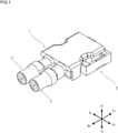
- FIG. 1 is a perspective view of a connector set including the plug of the first embodiment.
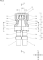
- FIG. 2 is a perspective view of the plug of the first embodiment.
- FIG. 3 is a top view of the plug of the first embodiment.
- FIG. 4 is a bottom view of the plug of the first embodiment.
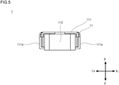
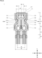
- FIG. 5 is a plan view of the plug of the first embodiment when viewed from the front.
- FIG. 6 is a plan view of the plug of the first embodiment when viewed from the rear.
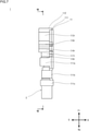
- FIG. 7 is a right side view of the plug of the first embodiment.
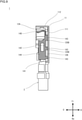
- FIG. 8 is a cross-sectional view taken along the line VIII-VIII of FIG.
- FIG. 9 is a cross-sectional view taken along the line IX-IX of FIG. FIG.
- FIG. 10 is a cross-sectional view taken along the line XX of FIG.
- FIG. 11 is a cross-sectional view taken along the line XI-XI of FIG.
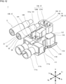
- FIG. 12 is a perspective view showing each element of the plug of the first embodiment in an exploded manner.
- FIG. 13 is a perspective view of the receptacle of the first embodiment.
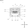
- FIG. 14 is a bottom view of the receptacle of the first embodiment.
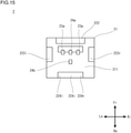
- FIG. 15 is a top view of the receptacle of the first embodiment.
- FIG. 16 is a right side view of the connector set of the first embodiment.
- FIG. 17 is a cross-sectional view taken along the line XVII-XVII of FIG. FIG.
- FIG. 18 is a cross-sectional view taken along the line XVIII-XVIII of FIG.
- FIG. 19 is a perspective view showing a modified example of the receptacle of the first embodiment.
- FIG. 20 is a perspective view of the plug of the second embodiment.
- FIG. 21 is a cross-sectional view of the plug of the second embodiment corresponding to FIG.
- FIG. 22 is a cross-sectional view of the plug of the second embodiment corresponding to FIG.
- FIG. 23 is a perspective view of a connector set including the plug of the third embodiment.
- FIG. 24 is a perspective view of the plug of the third embodiment.
- FIG. 25 is a perspective view of the receptacle of the third embodiment.
- FIG. 26 is a perspective view of the receptacle of the fourth embodiment.
- FIG. 27 is a perspective view of a connector set including the receptacle of the fourth embodiment.
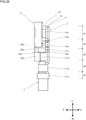
- FIG. 28 is a right side view of the connector set of the fourth embodiment.
- the plug according to this embodiment is connected to a transmission line including a signal line and a ground conductor.
- the plug includes a case, a holder, and a signal terminal.
- the case is conductive, has a bottom wall and has an opening on the top surface.
- the case includes a main fitting region, a sub-fitting region extending behind the main fitting region, a connection caulking region extending behind the sub-fitting region, and a ground caulking region extending behind the connection caulking region.
- the main fitting area comprises a front wall, a right wall and a left wall.
- the sub-fitting area comprises a right wall and a left wall.
- the caulking area comprises a right wall and a left wall.
- the ground caulking region is connected to the ground conductor of the transmission line.
- the holder is insulating and is held inside the case.
- the signal terminal is formed of a conductive member and is held by a holder.
- the signal terminal includes a signal terminal front end portion, a signal terminal rear end portion, and a signal terminal intermediate portion.
- the front end of the signal terminal is located in the main fitting area of the case and is exposed in the opening of the case.
- the rear end of the signal terminal is arranged in the connection caulking region of the case and is connected to the signal line of the transmission line.
- the intermediate portion of the signal terminal connects the front end portion of the signal terminal and the rear end portion of the signal terminal.
- the distance between the right wall and the left wall in the sub-fitting area is smaller than the distance between the right wall and the left wall in the main fitting area.
- the distance between the right wall and the left wall in the sub-fitting region is smaller than the distance between the right wall and the left wall in the connection caulking region.
- the case includes a first sub-right wall, a first sub-left wall, a second sub-right wall, and a second sub-left wall.
- the first sub-right wall connects the right wall of the main fitting region and the right wall of the sub-fitting region.
- the first sub-left wall connects the left wall of the main fitting region and the left wall of the sub-fitting region.
- the second sub-right wall connects the right wall of the connection caulking region and the right wall of the sub-fitting region.
- the second sub-left wall connects the left wall of the connection caulking region and the left wall of the sub-fitting region (first configuration).
- the plug of the first configuration electrically connects the transmission line connected to the plug (eg, coaxial cable, flexible circuit board, etc.) and the circuit board of the other party (eg, rigid circuit board, flexible circuit board, etc.).
- the signal line of the transmission line is connected to the rear end of the signal terminal.
- the ground conductor of the transmission line is electrically connected to the plug case. Behind the caulking region, that is, behind the signal terminal, the ground conductor of the transmission line is exposed.
- the front end of the signal terminal of the plug comes into contact with the signal line of the circuit board of the other party.
- the front end of the signal terminal of the plug may come into contact with the terminal connected to the signal line of the circuit board of the other party.
- the plug of the first configuration the following effects can be obtained. First, even if noise is generated at the front end of the signal terminal that is in direct or indirect contact with the signal line of the other circuit board, the first sub-right wall and the first sub-left wall move to the sub-fitting region of the noise. Propagation is blocked. Therefore, in the case of the plug, it is possible to suppress the noise generated at the front end of the signal terminal from entering the sub-fitting region, the connection caulking region, and the ground caulking region. As a result, the noise generated at the front end of the signal terminal does not easily reach the ground conductor of the transmission line exposed behind the signal terminal.
- the propagation of the noise to the sub-fitting region is blocked by the second sub-right wall and the second sub-left wall. Be done. Therefore, in the case of the plug, it is possible to suppress the noise generated behind the signal terminal from entering the sub-fitting region and the main fitting region. As a result, the noise generated behind the signal terminal does not easily reach the front end of the signal terminal of the plug.
- the plug of the first configuration it is possible to suppress the traffic of noise around the signal terminal in the case. As a result, the transmission signal becomes stable. That is, deterioration of the transmission signal can be suppressed.
- the other plug according to this embodiment is connected to a transmission line including a signal line and a ground conductor.
- the plug comprises a case, a holder, and two signal terminals.
- the case is conductive, has a bottom wall and has an opening on the top surface.
- the case includes a main fitting region, a sub-fitting region extending behind the main fitting region, a connection caulking region extending behind the sub-fitting region, and a ground caulking region extending behind the connection caulking region.
- the main fitting area comprises a front wall, a right wall and a left wall.
- the sub-fitting area comprises a right wall and a left wall.
- the caulking area comprises a right wall and a left wall.
- the ground caulking region is connected to the ground conductor of the transmission line.
- the holder is insulating and is held inside the case.
- the two signal terminals are formed of a conductive member, are arranged in parallel in the left-right direction with each other, and are held by a holder.
- Each of the signal terminals includes a signal terminal front end portion, a signal terminal rear end portion, and a signal terminal intermediate portion.
- the front end of the signal terminal is located in the main fitting area of the case and is exposed in the opening of the case.
- the rear end of the signal terminal is located in the caulking region of the case and is connected to the signal line of the corresponding transmission line.
- the intermediate portion of the signal terminal connects the front end portion of the signal terminal and the rear end portion of the signal terminal.
- the distance between the right wall and the left wall in the sub-fitting area is smaller than the distance between the right wall and the left wall in the main fitting area.
- the distance between the right wall and the left wall in the sub-fitting region is smaller than the distance between the right wall and the left wall in the connection caulking region.
- the case includes a first sub-right wall, a first sub-left wall, a second sub-right wall, and a second sub-left wall.
- the first sub-right wall connects the right wall of the main fitting region and the right wall of the sub-fitting region.
- the first sub-left wall connects the left wall of the main fitting region and the left wall of the sub-fitting region.
- the second sub-right wall connects the right wall of the connection caulking region and the right wall of the sub-fitting region.
- the second sub-left wall connects the left wall of the connection caulking region and the left wall of the sub-fitting region (second configuration).
- the plug of the second configuration electrically connects two transmission lines connected to the plug (eg, coaxial cable, flexible circuit board, etc.) and the circuit board of the other party (eg, rigid circuit board, flexible circuit board, etc.). Used to connect.
- the signal lines of the transmission line are connected to the rear end of the corresponding signal terminal.
- the ground conductor of the transmission line is electrically connected to the plug case. Behind the caulking region, that is, behind the signal terminal, the ground conductor of the transmission line is exposed.
- the front end of the signal terminal of the plug comes into contact with the signal line of the circuit board of the other party.
- the front end of the signal terminal of the plug may come into contact with the terminal connected to the signal line of the circuit board of the other party.
- the plug of the second configuration the following effects can be obtained in the same manner as the plug of the first configuration.
- the first sub-right wall and the first sub-left wall move to the sub-fitting region of the noise. Propagation is blocked. Therefore, in the case of the plug, it is possible to suppress the noise generated at the front end of the signal terminal from entering the sub-fitting region, the connection caulking region, and the ground caulking region. As a result, the noise generated at the front end of the signal terminal does not easily reach the ground conductor of the transmission line exposed behind the signal terminal.
- the propagation of the noise to the sub-fitting region is blocked by the second sub-right wall and the second sub-left wall. Be done. Therefore, in the case of the plug, it is possible to suppress the noise generated behind the signal terminal from entering the sub-fitting region and the main fitting region. As a result, the noise generated behind the signal terminal does not easily reach the front end of the signal terminal of the plug.
- the plug of the second configuration it is possible to suppress the traffic of noise around the signal terminal in the case. As a result, the transmission signal becomes stable. That is, deterioration of the transmission signal can be suppressed.
- the transmission line is a coaxial cable.
- Coaxial cable includes a center conductor (core wire) and an outer conductor (braided wire).
- the central conductor is the signal line and the outer conductor is the ground (GND) conductor.
- the rear end of the signal terminal of the plug includes the socket part.
- the center conductor is exposed in the caulking region, and the exposed center conductor is inserted into the socket portion. Then, by caulking the coaxial cable in the caulking region, the central conductor is connected to the rear end of the signal terminal. That is, the center conductor of the coaxial cable is connected to the signal terminal of the plug. Also, the outer conductor is exposed in the ground caulking region. By caulking the coaxial cable in the ground caulking region, the outer conductor of the coaxial cable is electrically connected to the case of the plug.
- the transmission line is a flexible circuit board.
- Flexible circuit boards include signal lines and ground (GND) conductors.
- the flexible circuit board includes a first region and a second region extending outside the first region.
- the first region has a stripline structure and includes a signal line, two ground conductors sandwiching the signal line between them, and an insulating layer insulating between the signal line and the ground conductor.
- the two ground conductors are removed and the insulating layer covering the signal lines is exposed.
- two ground conductors may be connected to each other at predetermined intervals along a signal line, or a plurality of ground vias connected to different ground portions of a flexible circuit board may be arranged. ..
- the ground conductor is electrically connected to the plug case. Further, in the connection caulking region, the socket portion at the rear end of the signal terminal is inserted into the insulating layer in the second region to sandwich the signal line. By crimping the second region in this state, the signal line is connected to the rear end of the signal terminal. That is, the signal line of the flexible circuit board is connected to the signal terminal of the plug.
- a readout electrode connected to the signal line may be provided on one surface of the insulating layer, and the readout electrode and the socket portion may be connected by solder or the like.
- the socket portion may have a flat plate shape so as to overlap the readout electrode.
- the distance between the right wall and the left wall in the sub-fitting region (hereinafter, may be abbreviated as “spacing D2”) is the distance between the right wall and the left in the main fitting region. It is smaller than the distance from the wall (hereinafter, may be abbreviated as “distance D1”) and is smaller than the distance between the right wall and the left wall in the connection caulking region (hereinafter, may be abbreviated as "distance D3"). As long as it is small, it is not particularly limited. However, from the viewpoint of sufficiently securing the first sub-right wall and the first sub-left wall, the interval D2 is preferably 4/5 or less of the interval D1.
- the interval D2 is preferably 4/5 or less of the interval D3.
- Each of these intervals D1, D2 and D3 means the shortest distance in the left-right direction from the inner surface of one wall to the inner surface of the other wall.
- the case is provided with protrusions on the left and right side edges of the bottom wall of the connection caulking region.
- each of the protrusions is bent to crimp the transmission line and surround the rear end of the signal terminal connected to the signal line of the transmission line together with the bottom wall (third configuration).
- the signal line of the transmission line is exposed due to the connection with the rear end of the signal terminal of the plug. Therefore, noise may be radiated from the exposed signal line.
- the rear end portion of the signal terminal is surrounded by the protruding portion and the bottom wall of the case, respectively, in the connection caulking region.
- the protruding portion and the bottom wall of the case are the ground (GND).
- the plug is provided with a ground terminal.
- the ground terminal is formed of a conductive member.
- the ground terminal is arranged in parallel with the signal terminal between the signal terminals and held in the holder.
- the ground terminal includes a ground terminal front end portion, a ground terminal rear end portion, and a ground terminal intermediate portion.
- the front end of the ground terminal is located in the main fitting area of the case and is exposed in the opening of the case.
- the rear end of the ground terminal is arranged in the caulking region of the case, is in contact with the bottom wall of the case, and is indirectly connected to the ground conductor of the transmission line.
- the ground terminal intermediate portion connects the front end portion of the ground terminal and the rear end portion of the ground terminal (fourth configuration).
- the ground terminal is arranged in parallel with the signal terminal between the signal terminals. In this case, the ground terminal absorbs noise between the signal terminals. Therefore, it is possible to suppress noise leakage from one signal terminal to the other signal terminal.
- the ground terminal preferably includes a plate portion protruding upward from the ground terminal intermediate portion and the ground terminal rear end portion (fifth configuration).
- the noise from one signal terminal to the other signal terminal is blocked by the plate portion of the ground terminal. Therefore, noise leakage from one signal terminal to the other signal terminal can be further suppressed.
- the case is provided with protrusions on the left and right side edges of the bottom wall of the connection caulking region.
- each of the protrusions is bent to crimp the transmission line and surround the rear end of the signal terminal connected to the signal line of the transmission line together with the bottom wall and the plate portion of the ground terminal (sixth configuration). ..
- the signal line of the transmission line is exposed due to the connection with the rear end of the signal terminal of the plug. Therefore, noise may be radiated from the exposed signal line.
- the rear end portion of the signal terminal is surrounded by the protruding portion and the bottom wall of the case, and the plate portion of the ground terminal, respectively, in the connection caulking region of the case. In this case, even if noise is radiated from the exposed signal line, the leakage of the noise to the outside of the case can be suppressed by the protruding portion and the bottom wall of the case and the plate portion of the ground terminal.
- each of the protruding portions of the case comes into contact with the upper edge of the plate portion of the ground terminal in the connection caulking region (seventh configuration).
- each of the protruding portions of the case is the plate portion of the ground terminal. Contact the upper edge. Therefore, the ground property of the ground terminal can be improved.
- the holder may have a right side surface and a left side surface.
- the right side surface of the holder is close to or in contact with the right wall of the sub-fitting area
- the left side surface of the holder is close to or in contact with the left wall of the sub-fitting area (eighth configuration).
- the plug fits into the receptacle mounted on the circuit board of the other party, for example.
- an inward pressing force is applied from the receptacle to the outer surfaces of the front wall, the right wall, and the left wall of the main fitting region of the case.
- an inward pressing force is also applied from the receptacle to the outer surfaces of the right wall and the left wall of the sub-fitting region of the case.
- the right wall and the left wall of the sub-fitting area of the case are displaced inward by the inward pressing force acting on the outer surfaces of the front wall, the right wall and the left wall of the main fitting area of the case, respectively. do. If this displacement is excessive, the inward pressing force acting on the outer surfaces of the right wall and the left wall of the sub-fitting region of the case is substantially weakened. Therefore, the fitting between the plug and the receptacle becomes loose, and the fitting state becomes unstable.
- the right side surface of the holder since the right side surface of the holder is close to the right wall of the sub-fitting area, excessive inward displacement of the right wall of the sub-fitting area is restricted. Similarly, the left side surface of the holder is in close proximity to the left wall of the sub-fitting area, limiting the excessive inward displacement of the left wall of the sub-fitting area. Further, if the right side surface of the holder is in contact with the right wall of the sub-fitting region, the right wall of the sub-fitting region is not displaced inward. Similarly, if the left side surface of the holder is in contact with the left wall of the sub-fitting region, the left wall of the sub-fitting region is not displaced inward.
- proximity means that the gap between the right side surface of the holder and the right wall of the sub-fitting area and the gap between the left side surface of the holder and the left wall of the sub-fitting area are more than 0 mm and 100 ⁇ m or less. means.
- the contact means a situation in which the gap between the right side surface of the holder and the right wall of the sub-fitting area and the gap between the left side surface of the holder and the left wall of the sub-fitting area are 0 mm.
- the right wall of the sub-fitting area may have a ridge that projects toward the right side surface of the holder, and the left wall of the sub-fitting area faces the left side surface of the holder. May have a protruding portion (9th configuration).
- the right side surface of the holder is close to or in contact with the raised portion of the right wall of the sub-fitting area
- the left side surface of the holder is close to or in contact with the raised portion of the left wall of the sub-fitting area. do. Therefore, the fitting between the plug and the receptacle becomes more stable.
- any one of the first to ninth configurations when the wavelength of the maximum frequency of the signal transmitted to the signal terminal is represented by ⁇ , it is preferable to satisfy the following conditions.
- the distance D2 between the right wall and the left wall in the sub-fitting region is larger than the heights of the right wall and the left wall in the sub-fitting region and smaller than 1/2 ⁇ ⁇ (10th configuration).
- the traffic of noise can be surely suppressed in the space existing around the signal terminal in the case in consideration of the frequency range of the signal transmitted to the signal terminal. .. Therefore, according to the plug having the tenth configuration, deterioration of the transmission signal can be further suppressed.
- any one of the first to ninth configurations when the wavelength of the maximum frequency of the signal transmitted to the signal terminal is represented by ⁇ and the relative permittivity of the holder is represented by ⁇ r, the following conditions are satisfied. Is preferable.
- the distance D2 between the right wall and the left wall in the sub-fitting region is larger than the heights of the right wall and the left wall in the sub-fitting region and smaller than 1/2 ⁇ ⁇ / ⁇ ( ⁇ r) (11th). Configuration).
- the traffic of noise can be surely suppressed by the holder existing around the signal terminal in the case in consideration of the frequency range of the signal transmitted to the signal terminal. .. Therefore, according to the plug of the eleventh configuration, deterioration of the transmission signal can be further suppressed.
- the connector set according to this embodiment includes a plug having any one of the first to eleventh configurations and a receptacle mounted on a circuit board and combined with the plug.
- the receptacle comprises a housing and an external terminal.
- the housing is insulating and accepts the main and sub-fitting areas of the plug case.
- the external terminals are conductive and are held in the housing.
- External terminals include a main front wall portion, a main right wall portion, a main left wall portion, a sub right wall portion, and a sub left wall portion.
- the main front wall portion comes into contact with the front wall of the main fitting area.
- the main right wall portion comes into contact with the right wall of the main fitting area.
- the main left wall portion comes into contact with the left wall of the main fitting area.
- the sub-right wall portion comes into contact with the right wall of the sub-fitting area.
- the sub-left wall portion comes into contact with the left wall of the sub-fitting region (12th configuration).
- the main front wall portion, the main right wall portion, the main left wall portion, the sub right wall portion, and the sub left wall portion are joined to the ground portion of the circuit board for the external terminals of the receptacle. Will be done. Then, the main front wall portion, the main right wall portion, and the main left wall portion each come into contact with the corresponding wall in the main fitting region of the plug, and the sub right wall portion and the sub left wall portion respectively subfit the plug. Contact the corresponding wall of the area. Therefore, the ground property of the plug case can be improved.
- the external terminal of the receptacle includes the connecting wall portion connecting the sub-right wall portion and the sub-left wall portion, and the connecting wall portion is preferably exposed on the back surface of the housing (13th). composition).
- the connecting wall portion of the receptacle can be joined to the ground portion of the circuit board. Therefore, the connecting wall portion, the sub-right wall portion, and the sub-left wall portion effectively become the ground (GND). Then, in the sub-fitting region, the signal terminal is surrounded by the bottom wall, the right wall and the left wall of the case, and the connecting wall portion, the sub-right wall portion and the sub-left wall portion of the receptacle. Therefore, it is possible to further suppress the entry of noise from the main fitting region to the sub-fitting region and the entry of noise from the connection caulking region to the sub-fitting region.
- the other connector set according to the present embodiment includes a plug having any one of the third, sixth, and seventh configurations, and a receptacle mounted on a circuit board and combined with the plug.
- the receptacle comprises a housing and an external terminal.
- the housing is insulating and accepts the main and sub-fitting areas of the plug case.
- the external terminals are conductive and are held in the housing.
- External terminals include a main front wall portion, a main right wall portion, a main left wall portion, a sub right wall portion, and a sub left wall portion.
- the main front wall portion comes into contact with the front wall of the main fitting area.
- the main right wall portion comes into contact with the right wall of the main fitting area.
- the main left wall portion comes into contact with the left wall of the main fitting area.
- the sub-right wall portion comes into contact with the right wall of the sub-fitting area.
- the sub-left wall portion comes into contact with the left wall of the sub-fitting area.
- the external terminal of the receptacle includes a connecting wall portion connecting the sub-right wall portion and the sub-left wall portion, and the connecting wall portion is exposed on the back surface of the housing.
- the external terminal of the receptacle includes an extension portion arranged behind the connecting wall portion, the sub-right wall portion, and the sub-left wall portion.
- the extending portion includes a base portion, a right standing portion, and a left standing portion.
- the base extends laterally, extending rearward from the connecting wall.
- the right standing portion stands up from the right end of the base and comes into contact with the right protruding portion of the left and right protrusions in the case of the plug.
- the left standing portion stands up from the left end of the base and comes into contact with the left protruding portion of the left and right protruding portions in the case of the plug (14th configuration).
- the main front wall portion, the main right wall portion, the main left wall portion, the sub right wall portion, and the sub left wall portion of the external terminals of the receptacle are respectively. , Joined to the ground part of the circuit board. Then, the main front wall portion, the main right wall portion, and the main left wall portion each come into contact with the corresponding wall in the main fitting region of the plug, and the sub right wall portion and the sub left wall portion respectively subfit the plug. Contact the corresponding wall of the area. Therefore, the ground property of the plug case can be improved.
- the connecting wall portion of the receptacle can be joined to the ground portion of the circuit board as in the 13th configuration. Therefore, the connecting wall portion, the sub-right wall portion, and the sub-left wall portion effectively become the ground (GND). Then, in the sub-fitting region, the signal terminal is surrounded by the bottom wall, the right wall and the left wall of the case, and the connecting wall portion, the sub-right wall portion and the sub-left wall portion of the receptacle. Therefore, it is possible to further suppress the entry of noise from the main fitting region to the sub-fitting region and the entry of noise from the connection caulking region to the sub-fitting region.
- the external terminal of the receptacle includes an extension portion, and the extension portion includes a base portion, a right standing portion, and a left standing portion. Then, the right upright portion and the left upright portion come into contact with the corresponding protrusions of the connection caulking region of the plug, respectively. In the caulking region, the protrusion of the plug surrounds the rear end of the signal terminal. In the sub-fitting region in front of the caulking region, the connecting wall portion of the receptacle is joined to the ground portion of the circuit board and electrically connected.
- the protruding portion of the plug is electrically connected to the connecting wall portion of the receptacle directly through the extending portion of the receptacle. Therefore, the electrical distance from the protrusion of the plug to the connecting wall of the receptacle is short.
- the connection caulking region where the protruding portion of the plug is present and the connecting wall portion of the receptacle are present.
- a ground potential difference is unlikely to occur between the sub-fitting region and the sub-fitting region. Therefore, it is possible to suppress the generation of noise due to the potential difference in the ground.
- FIG. 1 is a perspective view of a connector set including the plug 1 of the first embodiment.
- the connector set comprises a plug 1 and a receptacle 2.
- Two coaxial cables 3 are connected to the plug 1.
- a circuit board (not shown) is connected to the receptacle 2.
- the receptacle 2 accepts the plug 1 and is combined with the plug 1.
- the plug 1 is fitted to the receptacle 2, and each coaxial cable 3 and the circuit board (not shown) are electrically connected to each other.
- FIG. 2 is a perspective view of the plug 1.
- FIG. 3 is a top view of the plug 1.
- FIG. 4 is a bottom view of the plug 1.
- FIG. 5 is a plan view of the plug 1 when viewed from the front.
- FIG. 6 is a plan view of the plug 1 when viewed from the rear.
- FIG. 7 is a right side view of the plug 1.
- FIG. 8 is a cross-sectional view taken along the line VIII-VIII of FIG.
- FIG. 9 is a cross-sectional view taken along the line IX-IX of FIG.
- FIG. 10 is a cross-sectional view taken along the line XX of FIG.
- FIG. 11 is a cross-sectional view taken along the line XI-XI of FIG.
- FIG. 12 is a perspective view showing each element of the plug 1 in an exploded manner. 2 and 12 show a situation when the plug 1 is viewed from the upper surface side.
- the upper surface of the plug 1 means the surface facing the receptacle 2.
- the bottom surface of the plug 1 means a surface opposite to the surface facing the receptacle 2. Therefore, in the situation where the plug 1 is arranged below the receptacle 2, the upper surface of the plug 1 faces upward, and in the situation where the plug 1 is arranged above the receptacle 2, the upper surface of the plug 1 faces downward.
- the front-rear direction the direction in which the coaxial cable 3 extends
- the side where the coaxial cable 3 exists is called the rear, and the side opposite to it is called the front.
- the direction perpendicular to the front-back direction and the up-down direction is called the left-right direction.
- the top is indicated by U
- the bottom is indicated by D
- the front is indicated by Fr
- the rear is indicated by Re
- the right is indicated by Ri
- the left is indicated by Le.
- the coaxial cable 3 includes a central conductor 31, an insulator 33, an outer conductor 32, and a protective film 34 in order from the axis.
- the insulator 33 insulates the central conductor 31 from the outer conductor 32.
- the plug 1 includes a case 11, a holder 12, two signal terminals 13, and a ground terminal 14.
- the case 11 is conductive and includes an opening 110 on the upper surface.
- the case 11 is made of, for example, a metal plate.
- the case 11 is manufactured by bending a metal plate.
- the material of the case 11 (metal plate) is, for example, a copper alloy.
- the case 11 (metal plate) may be plated (eg, Ni (nickel) plating, Au (gold) plating).
- Case 11 includes a bottom wall 111.
- the bottom wall 111 is divided into a main fitting area A1, a sub-fitting area A2, and a connection caulking area A3 in order from the front side. That is, the sub-fitting region A2 is connected to the rear of the main fitting region A1, and the connection caulking region A3 is connected to the rear of the sub-fitting region A2.
- the portion of the sub-fitting region A2 is constricted.
- the ground caulking region A4 is connected behind the connection caulking region A3.
- the case 11 includes a main fitting region A1, a sub-fitting region A2, a connection caulking region A3, and a ground caulking region A4.
- the cable caulking region A5 is connected behind the ground caulking region A4.
- the main fitting region A1 includes a front wall 112, a right wall 113r, and a left wall 113l.
- the sub-fitting region A2 includes a right wall 114r and a left wall 114l.
- the connection caulking region A3 includes a right wall 115r and a left wall 115l.
- the distance D2 between the right wall 114r and the left wall 114l in the sub-fitting region A2 is set between the right wall 113r and the left wall 113l in the main fitting region A1. It is smaller than the distance D1 and smaller than the distance D3 between the right wall 115r and the left wall 115l in the connection caulking region A3 (see FIGS. 3 and 8).
- the case 11 further includes a first sub-right wall 116r, a first sub-left wall 116l, a second sub-right wall 117r, and a second sub-left wall 117l.
- the first sub-right wall 116r connects the right wall 113r of the main fitting region A1 and the right wall 114r of the sub-fitting region A2.
- the first sub-left wall 116l connects the left wall 113l of the main fitting region A1 and the left wall 114l of the sub-fitting region A2.
- the second sub-right wall 117r connects the right wall 115r of the connection caulking region A3 and the right wall 114r of the sub-fitting region A2.
- the second sub-left wall 117l connects the left wall 115l of the connection caulking region A3 and the left wall 114l of the sub-fitting region A2.
- These walls 112, 113r, 113l, 114r, 114l, 115r, 115l, 116r, 116l, 117r and 117l are integrated with the bottom wall 111 and project upward from the bottom wall 111.
- the upper surface located on the opposite side of the bottom wall 111 is the opening 110.
- the right wall 114r of the sub-fitting region A2 has a raised portion 114ra in the vicinity of the first sub-right wall 116r.
- the raised portion 114ra projects inward in the left-right direction. That is, the raised portion 114ra projects toward the right side surface 120Ar of the holder 12.
- the left wall 114l of the sub-fitting region A2 has a raised portion 114la in the vicinity of the first sub-left wall 116l.
- the raised portion 114la projects inward in the left-right direction. That is, the raised portion 114la projects toward the left side surface 120Al of the holder 12.
- protrusions 111a and 111a are provided on the left and right side edges of the bottom wall 111.
- Each of the protrusions 111a and 111a is bent inward to crimp the coaxial cable 3. More specifically, the tip of the central conductor 31 of the coaxial cable 3 is inserted into the socket portion 131a of the signal terminal rear end portion 131, which will be described in detail later, whereby the central conductor 31 is connected to the signal terminal 13. At this time, the center conductor 31 of the coaxial cable 3 is exposed due to the connection with the signal terminal rear end portion 131 of the plug 1.
- the insulator 33 of the coaxial cable 3 is sandwiched between each of the bent protrusions 111a and 111a and the bottom wall 111. As a result, the coaxial cable 3 is held in the case 11. In this way, in the connection caulking region A3, the signal terminal rear end 131 connected to the central conductor 31 of the coaxial cable 3 is surrounded by the protrusions 111a and 111a and the bottom wall 111 (see FIG. 10). ).
- each of the projecting portions 111a and 111a sandwiches the holder 12 together with the coaxial cable 3.
- the signal terminal 13 and the ground terminal 14, which will be described in detail later, are held in the case 11 together with the holder 12.
- cylinder portions 111b and 111b are provided at positions corresponding to the coaxial cables 3 respectively. Notches are provided in each of the tubular portions 111b and 111b, and each of the tubular portions 111b and 111b can be expanded or contracted. Each of the tubular portions 111b and 111b is integrated with the bottom wall 111 and is electrically connected to the bottom wall 111. Each of the tubular portions 111b and 111b is reduced and deformed to crimp the coaxial cable 3. More specifically, the outer conductor 32 of the coaxial cable 3 is exposed, and the exposed outer conductor 32 is inserted into the tubular portions 111b and 111b.
- the outer conductor 32 of the coaxial cable 3 is sandwiched between the reduced and deformed tubular portions 111b and 111b.
- the coaxial cable 3 is held in the case 11, and the case 11 is electrically connected to the outer conductor 32 of the coaxial cable 3.
- the cable caulking region A5 is provided with cylinder portions 111c and 111c at positions corresponding to the coaxial cables 3, respectively. Notches are provided in each of the tubular portions 111c and 111c, and each of the tubular portions 111c and 111c can be expanded or contracted. Each of the tubular portions 111c and 111c is integrated with the bottom wall 111 via the tubular portions 111b and 111b of the ground caulking region A4. Each of the tubular portions 111c and 111c is reduced and deformed to crimp the coaxial cable 3. More specifically, the coaxial cable 3 is inserted into the tubular portions 111c and 111c. Then, the protective film 34 of the coaxial cable 3 is sandwiched between the reduced and deformed tubular portions 111c and 111c. This ensures that the coaxial cable 3 is held in the case 11.
- the holder 12 has an insulating property. That is, the holder 12 is a dielectric.
- the holder 12 is held in the case 11.
- the holder 12 is made of, for example, a resin.
- the holder 12 is manufactured by injection molding.
- the material of the holder 12 is, for example, a liquid crystal polymer.
- the holder 12 is composed of a first holder 12A and a second holder 12B that are stacked on each other (see FIGS. 9 and 12).
- the first holder 12A is arranged on the opening 110 side of the case 11, and the second holder 12B is arranged on the bottom wall 111 side of the case 11.
- the first holder 12A and the second holder 12B hold two signal terminals 13 and a ground terminal 14, which will be described in detail later.
- the first holder 12A and the second holder 12B are individually injection molded. However, the second holder 12B may be insert-molded so as to be integrated with the case 11.
- the second holder 12B has a plate shape.
- the second holder 12B overlaps the bottom wall 111 of the case 11.
- the second holder 12B has a slit 120B at a position corresponding to the ground terminal 14, which will be described in detail later.
- the ground terminal 14 comes into contact with the bottom wall 111 of the case 11 through the slit 120B. As a result, the ground terminal 14 is electrically connected to the case 11 and eventually to the outer conductor 32 of the coaxial cable 3.
- the first holder 12A includes a base 120A and a recess 121A.
- the base 120A is housed in the sub-fitting area A2 of the case 11.
- the recess 121A is housed in the main fitting region A1 of the case 11.
- the right side surface 120Ar of the base portion 120A is close to the raised portion 114ra of the right wall 114r of the sub-fitting region A2.
- the left side surface 120Al of the base portion 120A is close to the raised portion 114la of the left wall 114l of the sub-fitting region A2.
- the right side surface 120Ar of the base portion 120A may come into contact with the raised portion 114ra of the right wall 114r of the sub-fitting region A2.
- the left side surface 120Al of the base portion 120A may come into contact with the raised portion 114la of the left wall 114l of the sub-fitting region A2.
- the recess 121A accommodates the signal terminal front end 130 of each signal terminal 13, which will be described in detail later, and the ground terminal front end 140 of the ground terminal 14. In the recess 121A, the portions corresponding to the front end 130 of each signal terminal and the front end 140 of the ground terminal penetrate.
- the two signal terminals 13 and the ground terminal 14 are held in the holder 12 (first holder 12A and second holder 12B). Specifically, the second holder 12B overlaps on the bottom wall 111 of the case 11, and two signal terminals 13 and a ground terminal 14 are arranged on the second holder 12B.
- the two signal terminals 13 are arranged in parallel with each other in the left-right direction.
- the ground terminal 14 is arranged in parallel with the signal terminal 13 between the signal terminals 13.
- Each signal terminal 13 and ground terminal 14 extend in the front-rear direction.
- the signal terminal 13 is formed of a conductive member.
- the signal terminal 13 is made of a metal plate. That is, the signal terminal 13 has conductivity.
- the signal terminal 13 is manufactured by bending an elongated metal plate.
- the material of the signal terminal 13 (metal plate) is, for example, a copper alloy.
- the signal terminal 13 (metal plate) may be plated (eg, Ni (nickel) plating, Au (gold) plating).
- the ground terminal 14 is formed of a conductive member.
- the ground terminal 14 is made of a metal plate. That is, the ground terminal 14 has conductivity.
- the ground terminal 14 is manufactured by bending an elongated metal plate.
- the material of the ground terminal 14 (metal plate) is, for example, a copper alloy.
- the ground terminal 14 (metal plate) may be plated (eg, Ni (nickel) plating, Au (gold) plating).
- the signal terminal 13 includes a signal terminal front end portion 130, a signal terminal rear end portion 131, and a signal terminal intermediate portion (not shown).
- the signal terminal intermediate portion connects the signal terminal front end portion 130 and the signal terminal rear end portion 131.
- the signal terminal front end portion 130 is located in front of the signal terminal intermediate portion and is arranged in the main fitting region A1 of the case 11.
- the signal terminal rear end portion 131 is located behind the signal terminal intermediate portion and is arranged in the connection caulking region A3.
- the signal terminal front end 130 bends toward the opening 110 of the case 11 and is exposed to the opening 110.
- the signal terminal 13 includes a socket portion 131a.
- the socket portion 131a stands up from the rear end of the signal terminal rear end portion 131.
- the socket portion 131a has a notch.
- the tip of the center conductor 31 of the coaxial cable 3 is inserted into the notch in the socket portion 131a.
- the coaxial cable 3 is caulked, and the center conductor 31 is connected to the rear end portion 131 of the signal terminal.
- the ground terminal 14 includes a ground terminal front end portion 140, a ground terminal rear end portion 141, and a ground terminal intermediate portion 142 (see FIG. 9).
- the ground terminal intermediate portion 142 connects the ground terminal front end portion 140 and the ground terminal rear end portion 141.
- the ground terminal front end portion 140 is located in front of the ground terminal intermediate portion 142 and is arranged in the main fitting region A1 of the case 11.
- the rear end portion 141 of the ground terminal is located behind the intermediate portion 142 of the ground terminal and is arranged in the connection caulking region A3.
- the front end portion 140 of the ground terminal bends toward the opening 110 of the case 11 and is exposed to the opening 110.
- each signal terminal 13 and the ground terminal 14 are held by the holder 12 (first holder 12A and second holder 12B) in the case 11. Specifically, each signal terminal 13 and ground terminal 14 are arranged on the second holder 12B. A second holder 12B exists between each signal terminal 13 and the bottom wall 111 of the case 11. Since the second holder 12B has an insulating property, the signal terminal 13 is insulated from the case 11.
- the second holder 12B also exists between the ground terminal 14 and the bottom wall 111 of the case 11.
- the second holder 12B has a slit 120B.
- the ground terminal 14 has a protrusion 143 at a position corresponding to the slit 120B, and the protrusion 143 contacts the bottom wall 111 of the case 11 through the slit 120B.
- the ground terminal 14 is electrically connected to the case 11.
- the ground terminal 14 is electrically connected to the outer conductor 32 of the coaxial cable 3 via the case 11.
- the protrusion 143 is provided at the rear end portion 141 of the ground terminal. Therefore, the ground terminal 14 is electrically connected to the bottom wall 111 of the case 11 at the rear end portion 141 of the ground terminal existing in the connection caulking region A3.
- the protrusion 143 is also provided on the ground terminal front end portion 140 and the ground terminal intermediate portion 142, and the second holder 12B is provided with a slit 120B at a position corresponding to each protrusion 143. Therefore, the ground terminal 14 is electrically connected to the bottom wall 111 of the case 11 even at the ground terminal front end portion 140 existing in the main fitting region A1 and the ground terminal intermediate portion 142 existing in the sub-fitting region A2.
- the ground terminal 14 includes the plate portion 144 (see FIGS. 3, 8 to 12).
- the plate portion 144 projects upward from the ground terminal intermediate portion 142 and the ground terminal rear end portion 141.
- the signal terminal rear end 131 connected to the central conductor 31 of the coaxial cable 3 has the protrusions 111a and 111a of the case 11 and the bottom wall 111 of the case 11. And surrounded by the plate portion 144 of the ground terminal 14. In this case, each of the protruding portions 111a and 111a of the case 11 comes into contact with the upper edge of the plate portion 144 of the ground terminal 14.
- the distance D2 between the right wall 114r and the left wall 114l in the sub-fitting region A2 satisfies the following condition (a).
- the interval D2 is larger than each height H1 of the right wall 114r and the left wall 114l in the sub-fitting region A2, and smaller than 1/2 ⁇ ⁇ .
- ⁇ means the wavelength of the maximum frequency of the signal transmitted to the signal terminal 13. Since the transmitted signal has a predetermined frequency range, the wavelength at the maximum value of the frequency range corresponds to ⁇ . For example, the frequency of the transmission signal is 20 GHz or higher.
- the interval D2 may satisfy the following condition (b) instead of the above condition (a).
- condition (b) The interval D2 is larger than each height H1 of the right wall 114r and the left wall 114l in the sub-fitting region A2, and smaller than 1/2 ⁇ ⁇ / ⁇ ( ⁇ r).
- ⁇ means the same as the above condition (a).
- ⁇ r means the relative permittivity of the holder 12. For example, when the material of the holder 12 is a liquid crystal polymer, its relative permittivity is 3 to 5.
- FIG. 13 is a perspective view of the receptacle 2.
- FIG. 14 is a bottom view of the receptacle 2.
- FIG. 15 is a top view of the receptacle 2.
- the surface and direction of the receptacle 2 conform to the surface and direction of the plug 1. That is, the bottom surface of the receptacle 2 means the surface facing the plug 1.
- the upper surface of the receptacle 2 means a surface opposite to the surface facing the plug 1. Therefore, in the situation where the receptacle 2 is arranged below the plug 1, the upper surface of the receptacle 2 faces downward, and in the situation where the receptacle 2 is arranged above the plug 1, the upper surface of the receptacle 2 faces upward.
- the receptacle 2 includes a housing 21 and an external terminal 22. Further, in the present embodiment, the receptacle 2 includes two signal terminals 23 and a ground terminal 24.
- the housing 21 has an insulating property.
- the housing 21 is made of, for example, a resin.
- the housing 21 is manufactured by injection molding.
- the material of the housing 21 is, for example, a liquid crystal polymer.
- the housing 21 holds two signal terminals 23 and a ground terminal 24, which will be described in detail later.
- the housing 21 may be insert-molded so as to be integrated with an external terminal 22, which will be described in detail later. Further, the housing 21 may be insert-molded so as to be integrated with each signal terminal 23 and the ground terminal 24.
- the housing 21 includes a recess 210.
- the recess 210 has a shape capable of receiving the main fitting region A1 and the sub-fitting region A2 in the case 11 of the plug 1. Therefore, the housing 21 includes a front wall 212, a right wall 213r, a left wall 213l, a right rear wall 214r, and a left rear wall 214l. Further, the housing 21 includes a top wall 211 which is the bottom of the recess 210. The top wall 211 can be read as a bottom wall when viewed as a single housing 21. In the state where the housing 21 receives the plug 1, the front wall 212 faces the front wall 112 of the main fitting region A1.
- the right wall 213r faces the right wall 113r of the main fitting region A1.
- the left wall 213l faces the left wall 113l of the main fitting region A1.
- the right rear wall 214r generally faces the first sub-right wall 116r.
- the left rear wall 214l generally faces the first sub-left wall 116l.
- the two signal terminals 23 and the ground terminal 24 are fixed to the top wall 211. Specifically, the two signal terminals 23 are arranged in parallel with each other in the left-right direction. The ground terminal 24 is arranged in parallel with the signal terminal 23 between the signal terminals 23.
- the signal terminal 23 is formed of a conductive member.
- the signal terminal 23 is made of a metal plate. That is, the signal terminal 23 has conductivity.
- the signal terminal 23 is manufactured by bending an elongated metal plate.
- the material of the signal terminal 23 (metal plate) is, for example, a copper alloy.
- the signal terminal 23 (metal plate) may be plated (eg, Ni (nickel) plating, Au (gold) plating).
- the ground terminal 24 is formed of a conductive member.
- the ground terminal 24 is made of a metal plate. That is, the ground terminal 24 has conductivity.
- the ground terminal 24 is manufactured by bending an elongated metal plate.
- the material of the ground terminal 24 (metal plate) is, for example, a copper alloy.
- the signal terminal 23 (metal plate) may be plated (eg, Ni (nickel) plating, Au (gold) plating).
- the signal terminal 23 has a convexly curved shape. One end portion 23a of the signal terminal 23 penetrates the top wall 211 and is exposed on the back surface of the top wall 211.
- the ground terminal 24 has a convexly curved shape. One end 24a and the other end 24b of the ground terminal 24 penetrate the top wall 211 and are exposed on the back surface of the top wall 211.
- the external terminal 22 has conductivity and is held in the housing 21.
- the external terminal 22 includes a main front wall portion 222, a main right wall portion 223r, a main left wall portion 223l, a sub right wall portion 224r, and a sub left wall portion 224l.
- the main front wall portion 222 is provided on the inner surface of the front wall 212 of the housing 21.
- the main right wall portion 223r is provided on the inner surface of the right wall 213r of the housing 21.
- the main left wall portion 223 l is provided on the inner surface of the left wall 213 l of the housing 21.
- the sub-right wall portion 224r is provided on the side surface of the right rear wall 214r of the housing 21.
- the sub-left wall portion 224 l is provided inside the left rear wall 214 l of the housing 21. Each wall portion 222, 223r, 223l, 224r and 224l is exposed on the back surface of the top wall 211 (see FIG. 15).
- the external terminal 22 includes a connecting wall portion 224i.
- the connecting wall portion 224i connects the sub-right wall portion 224r and the sub-left wall portion 224l along the top wall 211.
- the connecting wall portion 224i is also exposed on the back surface of the top wall 211 (see FIG. 15).
- the external terminal 22 is made of, for example, a metal plate.
- the external terminal 22 is manufactured by bending the metal plate.
- the material of the external terminal 22 (metal plate) is, for example, a copper alloy.
- the external terminal 22 (metal plate) may be plated (eg, Ni (nickel) plating, Au (gold) plating).
- Such a receptacle 2 is mounted on a circuit board (not shown).
- the circuit board is a flexible circuit board.
- signal line contacts are formed at the positions of the signal terminals 23 exposed on the back surface of the top wall 211.
- a ground (GND) portion is formed on the circuit board at the position of the ground terminal 24 exposed on the back surface of the top wall 211.
- ground (GND) portions are formed at positions of the wall portions 222, 223r, 223l, 224r, 224l, and 224i exposed on the back surface of the top wall 211.
- the receptacle 2 is superposed on the circuit board, and each signal terminal 23 of the receptacle 2 is joined to the contact of the corresponding signal line of the circuit board by soldering. As a result, each signal terminal 23 is electrically connected to the signal line of the circuit board.
- the ground terminal 24 of the receptacle 2 is also joined to the corresponding ground portion of the circuit board by soldering. As a result, the ground terminal 24 of the receptacle 2 is electrically connected to the ground portion of the circuit board.
- Each wall portion 222, 223r, 223l, 224r, 224l and 224i of the receptacle 2 is also joined to the corresponding ground portion of the circuit board by soldering. As a result, each wall portion 222, 223r, 223l, 224r, 224l and 224i of the receptacle 2 is electrically connected to the ground portion of the circuit board.
- FIG. 16 to 18 show a connector set in which the plug 1 of the first embodiment is combined with the receptacle 2.
- FIG. 16 is a right side view of the connector set.
- FIG. 17 is a cross-sectional view taken along the line XVII-XVII of FIG.
- FIG. 18 is a cross-sectional view taken along the line XVIII-XVIII of FIG.
- the plug 1 when the plug 1 is combined with the receptacle 2, the main fitting region A1 and the sub-fitting region A2 in the case 11 of the plug 1 are fitted with the receptacle 2.
- the main front wall portion 222 of the receptacle 2 comes into contact with the front wall 112 of the main fitting region A1.
- the main right wall portion 223r of the receptacle 2 comes into contact with the right wall 113r of the main fitting region A1.
- the main left wall portion 223 l of the receptacle 2 comes into contact with the left wall 113 l of the main fitting region A1.
- the sub-right wall portion 224r of the receptacle 2 comes into contact with the right wall 114r of the sub-fitting region A2.
- the sub-left wall portion 224l of the receptacle 2 comes into contact with the left wall 114l of the sub-fitting region A2.
- the signal terminal front end 130 of the plug 1 comes into contact with the signal terminal 23 of the receptacle 2.
- the signal terminal 13 of the plug 1 conducts with the signal terminal 23 of the receptacle 2.
- the ground terminal front end 140 of the plug 1 comes into contact with the ground terminal 24 of the receptacle 2.
- the ground terminal 14 of the plug 1 becomes conductive with the ground terminal 24 of the receptacle 2.
- the coaxial cable 3 connected to the plug 1 and the circuit board of the other party on which the receptacle 2 is mounted can be electrically connected.
- the receptacle 2 includes a signal terminal 23 and a ground terminal 24.
- the receptacle 2 does not have to include the signal terminal 23 and the ground terminal 24.
- the receptacle 2 in that case is shown in FIG.
- an opening 211a is provided in the top wall 211 of the receptacle 2.
- the receptacle 2 is mounted on a circuit board (not shown), and the contact points of the signal lines of the circuit board are arranged and the ground conductor is arranged in the opening 211a. Then, as the plug 1 and the receptacle 2 are fitted, the signal terminal front end 130 of the plug 1 is brought into direct contact with the contact of the signal line of the circuit board. Further, the ground terminal front end portion 140 of the plug 1 is brought into direct contact with the ground portion of the circuit board.
- Noise is likely to occur at the front end 130 of the signal terminal that comes into direct or indirect contact with the signal line of the circuit board of the other party.
- the plug 1 of the present embodiment even if noise is generated at the front end portion 130 of the signal terminal, the propagation of the noise to the sub-fitting region A2 is blocked by the first sub-right wall 116r and the first sub-left wall 116l. .. Therefore, in the case 11 of the plug 1, it is possible to suppress the noise generated at the front end portion 130 of the signal terminal from entering the sub-fitting region A2, the connection caulking region A3, and the ground caulking region A4. As a result, the noise generated at the front end 130 of the signal terminal does not easily reach the outer conductor 32 (ground conductor) of the coaxial cable 3 (transmission line) exposed behind the signal terminal 13.
- noise may be radiated from the outer conductor 32 of the coaxial cable 3 exposed behind the signal terminal 13.
- the noise is propagated to the sub-fitting region A2 by the second sub-right wall 117r and the second sub-left wall 117l. Is blocked. Therefore, it is possible to prevent noise generated behind the signal terminal 13 from entering the sub-fitting region A2 and the main fitting region A1 in the case 11 of the plug 1. As a result, the noise generated behind the signal terminal 13 is unlikely to reach the signal terminal front end 130 of the plug 1.
- the plug 1 of the present embodiment it is possible to suppress the traffic of noise around the signal terminal 13 in the case 11. As a result, deterioration of the transmission signal can be suppressed.
- the ground terminal 14 is arranged in parallel with the signal terminal 13 between the signal terminals 13. In this case, the ground terminal 14 absorbs the noise between the signal terminals 13. Therefore, it is possible to suppress noise leakage from one signal terminal 13 to the other signal terminal 13.
- the ground terminal 14 includes the plate portion 144.
- the plate portion 144 of the ground terminal 14 blocks the noise from one signal terminal 13 to the other signal terminal 13. Therefore, noise leakage from one signal terminal 13 to the other signal terminal 13 can be further suppressed.
- connection caulking region A3 of the case 11 the central conductor 31 (signal line) of the coaxial cable 3 (transmission line) is exposed. Therefore, noise may be radiated from the exposed center conductor 31.
- the signal terminal rear end portions 131 are the protrusions 111a and 111a of the case 11, the bottom wall 111 of the case 11, and the ground terminal 14, respectively. Surrounded by a plate portion 144. In this case, even if noise is radiated from the exposed center conductor 31, the protrusions 111a and 111a of the case 11, the bottom wall 111 of the case 11, and the plate portion 144 of the ground terminal 14 cause the noise to be emitted.
- each of the protruding portions 111a and 111a of the case 11, the bottom wall 111 of the case 11, and the plate portion 144 of the ground terminal 14 are grounded (GND).
- the rear end portion 141 of the ground terminal comes into contact with the bottom wall 111 of the case 11 and is indirectly connected to the outer conductor 32 (ground conductor) of the coaxial cable 3 (transmission line).
- each of the projecting portions 111a and 111a of the case 11 comes into contact with the upper edge of the plate portion 144 of the ground terminal 14. Therefore, the ground property of the ground terminal 14 can be improved.
- An inward pressing force acts from 223 l. Further, the right wall 114r of the sub-fitting region A2 of the case 11 comes into contact with the sub-right wall portion 224r of the external terminal 22. The left wall 114l of the sub-fitting region A2 of the case 11 comes into contact with the sub-left wall portion 224l of the external terminal 22. Due to these contacts, inward pressing force acts on the outer surfaces of the right wall 114r and the left wall 114l of the sub-fitting region A2 of the case 11 from the sub-right wall portion 224r and the sub-left wall portion 224l of the external terminal 22. ..
- the inward pressing force acting on the outer surfaces of the front wall 112, the right wall 113r and the left wall 113l of the main fitting region A1 of the case 11 causes the right wall 114r and the left of the sub-fitting region A2 of the case 11
- Each of the walls 114l is displaced inward. If this displacement is excessive, the inward pressing force acting on the outer surfaces of the right wall 114r and the left wall 114l of the sub-fitting region A2 of the case 11 is substantially weakened. Therefore, the fitting between the plug 1 and the receptacle 2 becomes loose, and the fitting state becomes unstable.
- the right side surface 120Ar of the base portion 120A of the holder 12 is close to the raised portion 114ra of the right wall 114r of the sub-fitting region A2. Therefore, the excessive inward displacement of the right wall 114r of the sub-fitting region A2 is limited.
- the left side surface 120Al of the base portion 120A of the holder 12 is close to the raised portion 114la of the left wall 114l of the sub-fitting region A2. Therefore, the excessive inward displacement of the left wall 114l of the sub-fitting region A2 is limited.
- the inward pressing force acting on the outer surfaces of the right wall 114r and the left wall 114l of the sub-fitting region A2 of the case 11 is not weakened. Therefore, the fitting between the plug 1 and the receptacle 2 is not loosened, and the fitting state is stable.
- the contact state between the right wall 114r of the sub-fitting area A2 of the case 11 and the sub-right wall portion 224r of the external terminal 22 is stable, and the left wall 114l of the sub-fitting area A2 of the case 11 and the sub of the external terminal 22 are subordinate.
- the contact state with the left wall portion 224l is stable. Therefore, the ground connection at these contact portions is stable.
- the main front wall portion 222, the main right wall portion 223r, the main left wall portion 223l, the sub right wall portion 224r, and the sub left wall portion 224l are circuits, respectively. It is joined to the ground part of the substrate. Then, the main front wall portion 222, the main right wall portion 223r, and the main left wall portion 223l come into contact with the corresponding walls 112, 113r, and 113l of the main fitting region A1 of the plug 1, respectively, and the sub right wall portion 224r and the sub The left wall portion 224l comes into contact with the corresponding walls 114r and 114l of the sub-fitting region A2 of the plug 1, respectively. Therefore, the ground property of the case 11 of the plug 1 can be improved.
- the connecting wall portion 224i of the receptacle 2 can be joined to the ground portion of the circuit board. Therefore, the connecting wall portion 224i, the sub-right wall portion 224r, and the sub-left wall portion 224l effectively become the ground (GND). Then, in the sub-fitting region A2, the signal terminal 13 is provided by the bottom wall 111 of the case 11, the right wall 114r and the left wall 114l, and the connecting wall portion 224i, the sub-right wall portion 224r, and the sub-left wall portion 224l of the receptacle 2. Besieged.
- FIG. 20 is a perspective view of the plug 1.
- FIG. 21 is a cross-sectional view corresponding to FIG.
- FIG. 22 is a cross-sectional view corresponding to FIG.
- the plug 1 of the present embodiment does not include the ground terminal 14 of the first embodiment. That is, in the plug 1, two signal terminals 13 are arranged in parallel in the case 11 in the left-right direction. There is no ground terminal between the signal terminals 13.
- the receptacle 2 does not include the ground terminal 24 of the first embodiment. That is, in the receptacle 2, the two signal terminals 23 are arranged in parallel with each other in the left-right direction. There is no ground terminal between the signal terminals 23.
- the signal terminal rear end 131 connected to the central conductor 31 of the coaxial cable 3 is the projecting portions 111a and 111a of the case 11, respectively, and the case. Surrounded by the bottom wall 111 of 11 (see FIG. 22).
- the case 11 includes the first sub-right wall 116r, the first sub-left wall 116l, the second sub-right wall 117r, and the second sub-left wall 117l.
- the effect is obtained.
- the signal terminal rear end portions 131 connected to the central conductor 31 of the coaxial cable 3 are the projecting portions 111a and 111a of the case 11, and the bottom wall 111 of the case 11, respectively. Since it is surrounded by, the effect of (4) above can be obtained. Moreover, the above-mentioned effects (6) to (8) can also be obtained.
- FIG. 23 is a perspective view of a connector set including the plug 1.
- FIG. 24 is a perspective view of the plug 1.
- FIG. 25 is a perspective view of the receptacle 2.
- the plug 1 of the present embodiment includes one signal terminal 13 of the first embodiment and does not include a ground terminal 14. That is, in the plug 1, one signal terminal 13 is arranged in the case 11. There is no ground terminal.
- the receptacle 2 includes one signal terminal 23 of the first embodiment and does not include a ground terminal 24. That is, one signal terminal 23 is arranged in the receptacle 2. There is no ground terminal.
- the case 11 includes the first sub-right wall 116r, the first sub-left wall 116l, the second sub-right wall 117r, and the second sub-left wall 117l.
- the effect is obtained.
- the above-mentioned effects (6) to (8) can also be obtained.
- FIG. 26 is a perspective view of the receptacle 2.
- FIG. 27 is a perspective view of a connector set including the receptacle 2.
- FIG. 28 is a right side view of the connector set.
- the external terminal 22 includes an extension portion 225 arranged behind the connecting wall portion 224i, the sub-right wall portion 224r, and the sub-left wall portion 224l.
- the extending portion 225 includes a base portion 225i, a right standing portion 225r, and a left standing portion 225l.
- the base portion 225i extends in the left-right direction while extending rearward from the connecting wall portion 224i.
- the right standing portion 225r stands up from the right end of the base portion 225i. From another viewpoint, the right standing portion 225r projects from the right end of the base portion 225i toward the protruding portion 111a of the case 11 of the plug 1.
- the left standing portion 225l stands up from the left end of the base portion 225i. From another viewpoint, the left standing portion 225l projects from the left end of the base portion 225i toward the protruding portion 111a of the case 11 of the plug 1.
- the plug 1 if the plug 1 is combined with the receptacle 2, the main fitting region A1 and the sub-fitting region A2 in the case 11 of the plug 1 will be the receptacle 2 as in the first embodiment. Fits with. Further, the connection caulking region A3 in the case 11 of the plug 1 fits with the receptacle 2. Specifically, the protruding portions 111a and 111a of the case 11 of the plug 1 are fitted with the extending portion 225 of the external terminal 22 of the receptacle 2.
- the right standing portion 225r of the receptacle 2 comes into contact with the right protruding portion 111a of the left and right protruding portions 111a and 111a in the case 11 of the plug 1.
- the left standing portion 225l of the receptacle 2 comes into contact with the left protruding portion 111a of the left and right protruding portions 111a and 111a in the case 11 of the plug 1.
- the case 11 of the plug 1 conducts with the external terminal 22 of the receptacle 2 in the connection caulking region A3.
- the protruding portions 111a and 111a of the plug 1 are directly electrically connected to the connecting wall portion 224i of the receptacle 2 through the extending portion 225 of the receptacle 2, and become a ground potential.
- the protruding portions 111a and 111a of the plug 1 surround the rear end portion 131 of the signal terminal.
- the connecting wall portion 224i of the receptacle 2 is joined to the ground portion of the circuit board and electrically connected. Since the protruding portions 111a and 111a of the plug 1 are electrically connected to the connecting wall portion 224i of the receptacle 2 directly through the extending portion 225 of the receptacle 2, the connecting wall of the receptacle 2 is directly connected to the protruding portions 111a and 111a of the plug 1. The electrical distance to section 224i is short.
- the protrusions 111a and 111a of the plug 1 pass through the bottom wall 111 of the connection caulking region A3, and further the bottom wall 111, the right wall 114r and the left of the sub-fitting region A2. Through the wall 114l, it is electrically connected to the connecting wall portion 224i of the receptacle 2. In this case, the electrical distance from the protrusions 111a and 111a of the plug 1 to the connecting wall portion 224i of the receptacle 2 is relatively long.
- connection caulking region A3 where the protruding portions 111a and 111a of the plug 1 exist and the connecting wall portion 224i of the receptacle 2 A ground potential difference is likely to occur between the sub-fitting region A2 and the sub-fitting region A2 in which the ground is present. If a ground potential difference occurs between the connection caulking region A3 and the sub-fitting region A2, resonance may occur and noise may occur.
- the connection caulking region where the protruding portions 111a and 111a of the plug 1 exist since the electrical distance from the protruding portions 111a and 111a of the plug 1 to the connecting wall portion 224i of the receptacle 2 is short, the connection caulking region where the protruding portions 111a and 111a of the plug 1 exist. A ground potential difference is unlikely to occur between A3 and the sub-fitting region A2 in which the connecting wall portion 224i of the receptacle 2 exists. Therefore, it is possible to suppress the generation of noise due to the potential difference in the ground.
- a circuit board eg, a flexible circuit board
- the plug 1 instead of the coaxial cable 3.
- Plug A1 Main fitting area A2: Sub-fitting area A3: Connection caulking area 11: Case 111: Bottom wall 112: Front wall 113r: Right wall 113l: Left wall 114r: Right wall 114l: Left wall 115r: Right Wall 115l: Left wall 116r: First secondary right wall 116l: First secondary left wall 117r: Second secondary right wall 117l: Second secondary left wall 12: Holder 120Ar: Right side surface 120Al: Left side surface 13: Signal terminal 130: Signal terminal front end 14: Ground terminal 140: Ground terminal front end 144: Plate 2: Receptacle 21: Housing 211: Top wall 22: External terminal 222: Main front wall 223r: Main right wall 223l: Main left wall 224r: Sub-right wall part 224l: Sub-left wall part 224i: Connecting wall part 23: Signal terminal 24: Ground terminal 3: Coaxial cable (transmission line)
Landscapes
- Details Of Connecting Devices For Male And Female Coupling (AREA)
- Coupling Device And Connection With Printed Circuit (AREA)
Abstract
Description
図1は、第1実施形態のプラグ1を備えるコネクタセットの斜視図である。図1を参照して、コネクタセットは、プラグ1とレセプタクル2とを備える。プラグ1には、2つの同軸ケーブル3が接続される。レセプタクル2には、回路基板(図示省略)が接続される。レセプタクル2はプラグ1を受け入れて、プラグ1と組み合わされる。これにより、プラグ1がレセプタクル2と嵌合し、各同軸ケーブル3と回路基板(図示省略)とが相互に電気的に接続される。
図2~図12に第1実施形態のプラグ1を示す。図2は、プラグ1の斜視図である。図3は、プラグ1の上面図である。図4は、プラグ1の底面図である。図5は、プラグ1を前方から見たときの平面図である。図6は、プラグ1を後方から見たときの平面図である。図7は、プラグ1の右側面図である。図8は、図7の線VIII-VIIIにおける断面図である。図9は、図3の線IX-IXにおける断面図である。図10は、図3の線X-Xにおける断面図である。図11は、図3の線XI-XIにおける断面図である。図12は、プラグ1の各要素を分解して示す斜視図である。図2及び図12には、プラグ1を上面側から見たときの状況が示される。
(条件(a))
間隔D2は、副嵌合領域A2における右壁114r及び左壁114lの各高さH1よりも大きくて、1/2×λよりも小さい。ここで言うλは、信号端子13に伝送される信号の最大周波数の波長を意味する。伝送信号は所定の周波数域を有するため、その周波数域の最大値での波長がλに相当する。例えば、伝送信号の周波数は20GHz以上である。
(条件(b))
間隔D2は、副嵌合領域A2における右壁114r及び左壁114lの各高さH1よりも大きくて、1/2×λ/√(εr)よりも小さい。ここで言うλは、上記の条件(a)と同じものを意味する。εrは、ホルダ12の比誘電率を意味する。例えば、ホルダ12の材質が液晶ポリマの場合、その比誘電率は3~5である。
図13~図15に、第1実施形態のプラグ1と組み合わされるレセプタクル2を示す。図13は、レセプタクル2の斜視図である。図14は、レセプタクル2の底面図である。図15は、レセプタクル2の上面図である。
図16~図18に、第1実施形態のプラグ1がレセプタクル2と組み合わされたコネクタセットを示す。図16は、コネクタセットの右側面図である。図17は、図16の線XVII-XVIIにおける断面図である。図18は、図16の線XVIII-XVIIIにおける断面図である。
本実施形態のプラグ1及びコネクタセットによれば、以下の効果が得られる。
以下に、図20~図22を参照して第2実施形態を説明する。第2実施形態は、上記第1実施形態のプラグ1を変形したものである。以下、第1実施形態と重複する構成についての説明は適宜省略する。後述する実施形態でも同様とする。図20は、プラグ1の斜視図である。図21は、図8に相当する断面図である。図22は、図10に相当する断面図である。
以下に、図23~図25を参照して第3実施形態を説明する。第3実施形態は、上記第1実施形態のプラグ1を変形したものである。図23は、プラグ1を備えるコネクタセットの斜視図である。図24は、プラグ1の斜視図である。図25は、レセプタクル2の斜視図である。
以下に、図26~図28を参照して第4実施形態を説明する。第4実施形態は、上記第1実施形態のレセプタクル2を変形したものである。図26は、レセプタクル2の斜視図である。図27は、レセプタクル2を備えるコネクタセットの斜視図である。図28は、コネクタセットの右側面図である。
A1:主嵌合領域
A2:副嵌合領域
A3:結線かしめ領域
11:ケース
111:底壁
112:前壁
113r:右壁
113l:左壁
114r:右壁
114l:左壁
115r:右壁
115l:左壁
116r:第1副右壁
116l:第1副左壁
117r:第2副右壁
117l:第2副左壁
12:ホルダ
120Ar:右側面
120Al:左側面
13:信号端子
130:信号端子前端部
14:グラウンド端子
140:グラウンド端子前端部
144:板部
2:レセプタクル
21:ハウジング
211:天壁
22:外部端子
222:主前壁部
223r:主右壁部
223l:主左壁部
224r:副右壁部
224l:副左壁部
224i:連結壁部
23:信号端子
24:グラウンド端子
3:同軸ケーブル(伝送線路)
Claims (14)
- 信号線及びグラウンド導体を含む伝送線路が接続されるプラグであって、
当該プラグは、
導電性を有し、底壁を備えるとともに上面に開口を有するケースであって、
前壁、右壁及び左壁を備える主嵌合領域、
前記主嵌合領域の後方に連なり、右壁及び左壁を備える副嵌合領域、
前記副嵌合領域の後方に連なり、右壁及び左壁を備える結線かしめ領域、及び
前記結線かしめ領域の後方に連なり、前記伝送線路の前記グラウンド導体に接続されるグラウンドかしめ領域、を含む前記ケースと、
絶縁性を有し、前記ケース内に保持されるホルダと、
導電性部材で形成され、前記ホルダに保持される信号端子であって、
前記ケースの前記主嵌合領域に配置され、前記ケースの前記開口に表出する信号端子前端部、
前記ケースの前記結線かしめ領域に配置され、前記伝送線路の前記信号線に接続される信号端子後端部、及び
前記信号端子前端部と前記信号端子後端部とをつなぐ信号端子中間部、を含む前記信号端子と、を備え、
前記副嵌合領域における前記右壁と前記左壁との間隔が、前記主嵌合領域における前記右壁と前記左壁との間隔よりも小さく、
前記副嵌合領域における前記右壁と前記左壁との間隔が、前記結線かしめ領域における前記右壁と前記左壁との間隔よりも小さく、
前記ケースは、
前記主嵌合領域の前記右壁と前記副嵌合領域の前記右壁とをつなぐ第1副右壁と、
前記主嵌合領域の前記左壁と前記副嵌合領域の前記左壁とをつなぐ第1副左壁と、
前記結線かしめ領域の前記右壁と前記副嵌合領域の前記右壁とをつなぐ第2副右壁と、
前記結線かしめ領域の前記左壁と前記副嵌合領域の前記左壁とをつなぐ第2副左壁と、を備える、プラグ。 - 各々が信号線及びグラウンド導体を含む2つの伝送線路が接続されるプラグであって、
当該プラグは、
導電性を有し、底壁を備えるとともに上面に開口を有するケースであって、
前壁、右壁及び左壁を備える主嵌合領域、
前記主嵌合領域の後方に連なり、右壁及び左壁を備える副嵌合領域、
前記副嵌合領域の後方に連なり、右壁及び左壁を備える結線かしめ領域、及び
前記結線かしめ領域の後方に連なり、前記伝送線路の前記グラウンド導体に接続されるグラウンドかしめ領域、を含む前記ケースと、
絶縁性を有し、前記ケース内に保持されるホルダと、
導電性部材で形成され、相互に左右方向で並列に配置されて前記ホルダに保持される2つの信号端子であって、各々が、
前記ケースの前記主嵌合領域に配置され、前記ケースの前記開口に表出する信号端子前端部、
前記ケースの前記結線かしめ領域に配置され、対応する前記伝送線路の前記信号線に接続される信号端子後端部、及び
前記信号端子前端部と前記信号端子後端部とをつなぐ信号端子中間部、を含む前記信号端子と、を備え、
前記副嵌合領域における前記右壁と前記左壁との間隔が、前記主嵌合領域における前記右壁と前記左壁との間隔よりも小さく、
前記副嵌合領域における前記右壁と前記左壁との間隔が、前記結線かしめ領域における前記右壁と前記左壁との間隔よりも小さく、
前記ケースは、
前記主嵌合領域の前記右壁と前記副嵌合領域の前記右壁とをつなぐ第1副右壁と、
前記主嵌合領域の前記左壁と前記副嵌合領域の前記左壁とをつなぐ第1副左壁と、
前記結線かしめ領域の前記右壁と前記副嵌合領域の前記右壁とをつなぐ第2副右壁と、
前記結線かしめ領域の前記左壁と前記副嵌合領域の前記左壁とをつなぐ第2副左壁と、を備える、プラグ。 - 請求項2に記載のプラグであって、
前記ケースは、前記結線かしめ領域の前記底壁の左右の側縁に突出部を備え、
前記突出部の各々は、折り曲げられて前記伝送線路をかしめ、前記伝送線路の前記信号線に接続された前記信号端子後端部を、前記底壁と共に包囲する、プラグ。 - 請求項2に記載のプラグであって、
当該プラグは、
導電性部材で形成され、前記信号端子同士の間に前記信号端子と並列に配置されて前記ホルダに保持されるグラウンド端子を備え、
前記グラウンド端子は、
前記ケースの前記主嵌合領域に配置され、前記ケースの前記開口に表出するグラウンド端子前端部、
前記ケースの前記結線かしめ領域に配置され、前記ケースの前記底壁と接触して前記伝送線路の前記グラウンド導体に間接的に接続されるグラウンド端子後端部、及び
前記グラウンド端子前端部と前記グラウンド端子後端部とをつなぐグラウンド端子中間部、を含む、プラグ。 - 請求項4に記載のプラグであって、
前記グラウンド端子は、前記グラウンド端子中間部及び前記グラウンド端子後端部から上方に突出する板部を含む、プラグ。 - 請求項5に記載のプラグであって、
前記ケースは、前記結線かしめ領域の前記底壁の左右の側縁に突出部を備え、
前記突出部の各々は、折り曲げられて前記伝送線路をかしめ、前記伝送線路の前記信号線に接続された前記信号端子後端部を、前記底壁及び前記グラウンド端子の前記板部と共に包囲する、プラグ。 - 請求項6に記載のプラグであって、
前記結線かしめ領域において、前記ケースの前記突出部の各々が前記グラウンド端子の前記板部の上縁と接触する、プラグ。 - 請求項1~7のいずれか1項に記載のプラグであって、
前記ホルダは右側面及び左側面を有し、
前記ホルダの前記右側面が前記副嵌合領域の前記右壁と近接又は接触し、
前記ホルダの前記左側面が前記副嵌合領域の前記左壁と近接又は接触する、プラグ。 - 請求項8に記載のプラグであって、
前記副嵌合領域の前記右壁は、前記ホルダの前記右側面に向けて突出する隆起部を有し、
前記副嵌合領域の前記左壁は、前記ホルダの前記左側面に向けて突出する隆起部を有する、プラグ。 - 請求項1~9のいずれか1項に記載のプラグであって、
前記信号端子に伝送される信号の最大周波数の波長をλで表したとき、前記副嵌合領域における前記右壁と前記左壁との間隔は、前記副嵌合領域における前記右壁及び前記左壁の各高さよりも大きくて、1/2×λよりも小さい、プラグ。 - 請求項1~9のいずれか1項に記載のプラグであって、
前記信号端子に伝送される信号の最大周波数の波長をλで表し、前記ホルダの比誘電率をεrで表したとき、前記副嵌合領域における前記右壁と前記左壁との間隔は、前記副嵌合領域における前記右壁及び前記左壁の各高さよりも大きくて、1/2×λ/√(εr)よりも小さい、プラグ。 - 請求項1~11のいずれか1項に記載のプラグと、
回路基板に実装されて前記プラグと組み合わされるレセプタクルと、を備えるコネクタセットであって、
前記レセプタクルは、
絶縁性を有し、前記プラグの前記ケースのうちの前記主嵌合領域及び前記副嵌合領域を受け入れるハウジングと、
導電性を有し、前記ハウジングに保持される外部端子であって、
前記主嵌合領域の前記前壁と接触する主前壁部、
前記主嵌合領域の前記右壁と接触する主右壁部、
前記主嵌合領域の前記左壁と接触する主左壁部、
前記副嵌合領域の前記右壁と接触する副右壁部、及び
前記副嵌合領域の前記左壁と接触する副左壁部、を含む前記外部端子と、を備える、コネクタセット。 - 請求項12に記載のコネクタセットであって、
前記レセプタクルの前記外部端子は、前記副右壁部と前記副左壁部とをつなぐ連結壁部を含み、前記連結壁部は前記ハウジングの裏面に露出する、コネクタセット。 - 請求項3、6及び7のいずれか1項に記載のプラグと、
回路基板に実装されて前記プラグと組み合わされるレセプタクルと、を備えるコネクタセットであって、
前記レセプタクルは、
絶縁性を有し、前記プラグの前記ケースのうちの前記主嵌合領域及び前記副嵌合領域を受け入れるハウジングと、
導電性を有し、前記ハウジングに保持される外部端子であって、
前記主嵌合領域の前記前壁と接触する主前壁部、
前記主嵌合領域の前記右壁と接触する主右壁部、
前記主嵌合領域の前記左壁と接触する主左壁部、
前記副嵌合領域の前記右壁と接触する副右壁部、及び
前記副嵌合領域の前記左壁と接触する副左壁部、を含む前記外部端子と、を備え、
前記レセプタクルの前記外部端子は、前記副右壁部と前記副左壁部とをつなぐ連結壁部を含み、前記連結壁部は前記ハウジングの裏面に露出しており、
さらに、前記レセプタクルの前記外部端子は、前記連結壁部、前記副右壁部及び前記副左壁部の後方に配置される延出部を含み、
前記延出部は、
前記連結壁部から後方に延びつつ、左右方向に広がる基部と、
前記基部の右端から起立する右起立部であって、前記プラグの前記ケースにおける左右の前記突出部のうちの右側の前記突出部と接触する前記右起立部と、
前記基部の左端から起立する左起立部であって、前記プラグの前記ケースにおける左右の前記突出部のうちの左側の前記突出部と接触する前記左起立部と、を含む、コネクタセット。
Priority Applications (2)
| Application Number | Priority Date | Filing Date | Title |
|---|---|---|---|
| CN202190000636.XU CN220569998U (zh) | 2020-07-31 | 2021-07-07 | 插头和连接器组件 |
| JP2022540116A JP7235175B2 (ja) | 2020-07-31 | 2021-07-07 | プラグ及びコネクタセット |
Applications Claiming Priority (2)
| Application Number | Priority Date | Filing Date | Title |
|---|---|---|---|
| JP2020-130889 | 2020-07-31 | ||
| JP2020130889 | 2020-07-31 |
Publications (1)
| Publication Number | Publication Date |
|---|---|
| WO2022024697A1 true WO2022024697A1 (ja) | 2022-02-03 |
Family
ID=80036241
Family Applications (1)
| Application Number | Title | Priority Date | Filing Date |
|---|---|---|---|
| PCT/JP2021/025624 Ceased WO2022024697A1 (ja) | 2020-07-31 | 2021-07-07 | プラグ及びコネクタセット |
Country Status (3)
| Country | Link |
|---|---|
| JP (1) | JP7235175B2 (ja) |
| CN (1) | CN220569998U (ja) |
| WO (1) | WO2022024697A1 (ja) |
Citations (4)
| Publication number | Priority date | Publication date | Assignee | Title |
|---|---|---|---|---|
| JP2013125694A (ja) * | 2011-12-15 | 2013-06-24 | Jst Mfg Co Ltd | ベースコネクタ |
| JP2019197685A (ja) * | 2018-05-10 | 2019-11-14 | 第一精工株式会社 | ケーブルコネクタ装置 |
| JP2019220253A (ja) * | 2018-06-15 | 2019-12-26 | 日本圧着端子製造株式会社 | 同軸コネクタ |
| JP2020068163A (ja) * | 2018-10-26 | 2020-04-30 | 第一精工株式会社 | 同軸コネクタ装置 |
-
2021
- 2021-07-07 JP JP2022540116A patent/JP7235175B2/ja active Active
- 2021-07-07 WO PCT/JP2021/025624 patent/WO2022024697A1/ja not_active Ceased
- 2021-07-07 CN CN202190000636.XU patent/CN220569998U/zh active Active
Patent Citations (4)
| Publication number | Priority date | Publication date | Assignee | Title |
|---|---|---|---|---|
| JP2013125694A (ja) * | 2011-12-15 | 2013-06-24 | Jst Mfg Co Ltd | ベースコネクタ |
| JP2019197685A (ja) * | 2018-05-10 | 2019-11-14 | 第一精工株式会社 | ケーブルコネクタ装置 |
| JP2019220253A (ja) * | 2018-06-15 | 2019-12-26 | 日本圧着端子製造株式会社 | 同軸コネクタ |
| JP2020068163A (ja) * | 2018-10-26 | 2020-04-30 | 第一精工株式会社 | 同軸コネクタ装置 |
Also Published As
| Publication number | Publication date |
|---|---|
| JP7235175B2 (ja) | 2023-03-08 |
| JPWO2022024697A1 (ja) | 2022-02-03 |
| CN220569998U (zh) | 2024-03-08 |
Similar Documents
| Publication | Publication Date | Title |
|---|---|---|
| US7347721B2 (en) | Connector | |
| TWI442650B (zh) | Electrical connector | |
| CN103004034B (zh) | 连接器 | |
| US7892028B2 (en) | Cable connector assembly | |
| WO2000016449A1 (en) | Connector socket, connector plug and connector assembly | |
| US12347984B2 (en) | Electrical connector | |
| US8007325B2 (en) | Cable connecting apparatus | |
| US11769970B2 (en) | Connector and connector device | |
| US20100221933A1 (en) | Cable connector assembly with grounding device | |
| JP6721845B2 (ja) | フレキシブルケーブル用コネクタ、フレキシブルケーブル用アダプタ、及び、フレキシブルケーブル | |
| KR20090012085A (ko) | 커넥터 및 그것을 구비한 전자기기 | |
| US6674645B2 (en) | High frequency signal switching unit | |
| JP7387412B2 (ja) | コネクタ組立体 | |
| CN110416763B (zh) | 电连接器 | |
| US20250087917A1 (en) | Connector set and connector | |
| JP7235175B2 (ja) | プラグ及びコネクタセット | |
| JP5114297B2 (ja) | グランドバー及びケーブルアセンブリ | |
| US20240213726A1 (en) | Electrical connector with ground contact | |
| TW202431732A (zh) | 連接器裝置 | |
| WO2022004398A1 (ja) | 第1コネクタ、第2コネクタ、及びコネクタセット | |
| JP2022141246A (ja) | 電気コネクタ | |
| US20250062574A1 (en) | Electrical-connector-equipper cable | |
| EP4391247A1 (en) | Cable connector | |
| US7651377B2 (en) | Electrical card connector assembly | |
| JP7363228B2 (ja) | コネクタ装置、コネクタ、及びコネクタ構造 |
Legal Events
| Date | Code | Title | Description |
|---|---|---|---|
| 121 | Ep: the epo has been informed by wipo that ep was designated in this application |
Ref document number: 21849234 Country of ref document: EP Kind code of ref document: A1 |
|
| ENP | Entry into the national phase |
Ref document number: 2022540116 Country of ref document: JP Kind code of ref document: A |
|
| WWE | Wipo information: entry into national phase |
Ref document number: 202190000636.X Country of ref document: CN |
|
| NENP | Non-entry into the national phase |
Ref country code: DE |
|
| 122 | Ep: pct application non-entry in european phase |
Ref document number: 21849234 Country of ref document: EP Kind code of ref document: A1 |