WO2022024510A1 - 接着剤用組成物及びフィルム状接着剤、並びに、フィルム状接着剤を用いた半導体パッケージ及びその製造方法 - Google Patents
接着剤用組成物及びフィルム状接着剤、並びに、フィルム状接着剤を用いた半導体パッケージ及びその製造方法 Download PDFInfo
- Publication number
- WO2022024510A1 WO2022024510A1 PCT/JP2021/018947 JP2021018947W WO2022024510A1 WO 2022024510 A1 WO2022024510 A1 WO 2022024510A1 JP 2021018947 W JP2021018947 W JP 2021018947W WO 2022024510 A1 WO2022024510 A1 WO 2022024510A1
- Authority
- WO
- WIPO (PCT)
- Prior art keywords
- adhesive
- film
- phenoxy resin
- inorganic filler
- mass
- Prior art date
- Legal status (The legal status is an assumption and is not a legal conclusion. Google has not performed a legal analysis and makes no representation as to the accuracy of the status listed.)
- Ceased
Links
- 0 CC(C)(NC)O*C(C)=C Chemical compound CC(C)(NC)O*C(C)=C 0.000 description 1
Images



Classifications
-
- C—CHEMISTRY; METALLURGY
- C09—DYES; PAINTS; POLISHES; NATURAL RESINS; ADHESIVES; COMPOSITIONS NOT OTHERWISE PROVIDED FOR; APPLICATIONS OF MATERIALS NOT OTHERWISE PROVIDED FOR
- C09J—ADHESIVES; NON-MECHANICAL ASPECTS OF ADHESIVE PROCESSES IN GENERAL; ADHESIVE PROCESSES NOT PROVIDED FOR ELSEWHERE; USE OF MATERIALS AS ADHESIVES
- C09J163/00—Adhesives based on epoxy resins; Adhesives based on derivatives of epoxy resins
-
- C—CHEMISTRY; METALLURGY
- C09—DYES; PAINTS; POLISHES; NATURAL RESINS; ADHESIVES; COMPOSITIONS NOT OTHERWISE PROVIDED FOR; APPLICATIONS OF MATERIALS NOT OTHERWISE PROVIDED FOR
- C09D—COATING COMPOSITIONS, e.g. PAINTS, VARNISHES OR LACQUERS; FILLING PASTES; CHEMICAL PAINT OR INK REMOVERS; INKS; CORRECTING FLUIDS; WOODSTAINS; PASTES OR SOLIDS FOR COLOURING OR PRINTING; USE OF MATERIALS THEREFOR
- C09D163/00—Coating compositions based on epoxy resins; Coating compositions based on derivatives of epoxy resins
-
- C—CHEMISTRY; METALLURGY
- C08—ORGANIC MACROMOLECULAR COMPOUNDS; THEIR PREPARATION OR CHEMICAL WORKING-UP; COMPOSITIONS BASED THEREON
- C08L—COMPOSITIONS OF MACROMOLECULAR COMPOUNDS
- C08L71/00—Compositions of polyethers obtained by reactions forming an ether link in the main chain; Compositions of derivatives of such polymers
-
- C—CHEMISTRY; METALLURGY
- C09—DYES; PAINTS; POLISHES; NATURAL RESINS; ADHESIVES; COMPOSITIONS NOT OTHERWISE PROVIDED FOR; APPLICATIONS OF MATERIALS NOT OTHERWISE PROVIDED FOR
- C09J—ADHESIVES; NON-MECHANICAL ASPECTS OF ADHESIVE PROCESSES IN GENERAL; ADHESIVE PROCESSES NOT PROVIDED FOR ELSEWHERE; USE OF MATERIALS AS ADHESIVES
- C09J11/00—Features of adhesives not provided for in group C09J9/00, e.g. additives
- C09J11/02—Non-macromolecular additives
- C09J11/04—Non-macromolecular additives inorganic
-
- C—CHEMISTRY; METALLURGY
- C09—DYES; PAINTS; POLISHES; NATURAL RESINS; ADHESIVES; COMPOSITIONS NOT OTHERWISE PROVIDED FOR; APPLICATIONS OF MATERIALS NOT OTHERWISE PROVIDED FOR
- C09J—ADHESIVES; NON-MECHANICAL ASPECTS OF ADHESIVE PROCESSES IN GENERAL; ADHESIVE PROCESSES NOT PROVIDED FOR ELSEWHERE; USE OF MATERIALS AS ADHESIVES
- C09J171/00—Adhesives based on polyethers obtained by reactions forming an ether link in the main chain; Adhesives based on derivatives of such polymers
-
- C—CHEMISTRY; METALLURGY
- C09—DYES; PAINTS; POLISHES; NATURAL RESINS; ADHESIVES; COMPOSITIONS NOT OTHERWISE PROVIDED FOR; APPLICATIONS OF MATERIALS NOT OTHERWISE PROVIDED FOR
- C09J—ADHESIVES; NON-MECHANICAL ASPECTS OF ADHESIVE PROCESSES IN GENERAL; ADHESIVE PROCESSES NOT PROVIDED FOR ELSEWHERE; USE OF MATERIALS AS ADHESIVES
- C09J7/00—Adhesives in the form of films or foils
- C09J7/10—Adhesives in the form of films or foils without carriers
-
- C—CHEMISTRY; METALLURGY
- C09—DYES; PAINTS; POLISHES; NATURAL RESINS; ADHESIVES; COMPOSITIONS NOT OTHERWISE PROVIDED FOR; APPLICATIONS OF MATERIALS NOT OTHERWISE PROVIDED FOR
- C09J—ADHESIVES; NON-MECHANICAL ASPECTS OF ADHESIVE PROCESSES IN GENERAL; ADHESIVE PROCESSES NOT PROVIDED FOR ELSEWHERE; USE OF MATERIALS AS ADHESIVES
- C09J7/00—Adhesives in the form of films or foils
- C09J7/30—Adhesives in the form of films or foils characterised by the adhesive composition
-
- H—ELECTRICITY
- H10—SEMICONDUCTOR DEVICES; ELECTRIC SOLID-STATE DEVICES NOT OTHERWISE PROVIDED FOR
- H10B—ELECTRONIC MEMORY DEVICES
- H10B80/00—Assemblies of multiple devices comprising at least one memory device covered by this subclass
-
- H—ELECTRICITY
- H10—SEMICONDUCTOR DEVICES; ELECTRIC SOLID-STATE DEVICES NOT OTHERWISE PROVIDED FOR
- H10P—GENERIC PROCESSES OR APPARATUS FOR THE MANUFACTURE OR TREATMENT OF DEVICES COVERED BY CLASS H10
- H10P95/00—Generic processes or apparatus for manufacture or treatments not covered by the other groups of this subclass
-
- H—ELECTRICITY
- H10—SEMICONDUCTOR DEVICES; ELECTRIC SOLID-STATE DEVICES NOT OTHERWISE PROVIDED FOR
- H10W—GENERIC PACKAGES, INTERCONNECTIONS, CONNECTORS OR OTHER CONSTRUCTIONAL DETAILS OF DEVICES COVERED BY CLASS H10
- H10W72/00—Interconnections or connectors in packages
- H10W72/071—Connecting or disconnecting
-
- H—ELECTRICITY
- H10—SEMICONDUCTOR DEVICES; ELECTRIC SOLID-STATE DEVICES NOT OTHERWISE PROVIDED FOR
- H10W—GENERIC PACKAGES, INTERCONNECTIONS, CONNECTORS OR OTHER CONSTRUCTIONAL DETAILS OF DEVICES COVERED BY CLASS H10
- H10W72/00—Interconnections or connectors in packages
- H10W72/30—Die-attach connectors
-
- H—ELECTRICITY
- H10—SEMICONDUCTOR DEVICES; ELECTRIC SOLID-STATE DEVICES NOT OTHERWISE PROVIDED FOR
- H10W—GENERIC PACKAGES, INTERCONNECTIONS, CONNECTORS OR OTHER CONSTRUCTIONAL DETAILS OF DEVICES COVERED BY CLASS H10
- H10W72/00—Interconnections or connectors in packages
- H10W72/30—Die-attach connectors
- H10W72/341—Dispositions of die-attach connectors, e.g. layouts
- H10W72/344—Dispositions of die-attach connectors, e.g. layouts relative to underlying supporting features, e.g. bond pads, RDLs or vias
-
- H—ELECTRICITY
- H10—SEMICONDUCTOR DEVICES; ELECTRIC SOLID-STATE DEVICES NOT OTHERWISE PROVIDED FOR
- H10W—GENERIC PACKAGES, INTERCONNECTIONS, CONNECTORS OR OTHER CONSTRUCTIONAL DETAILS OF DEVICES COVERED BY CLASS H10
- H10W90/00—Package configurations
-
- H—ELECTRICITY
- H10—SEMICONDUCTOR DEVICES; ELECTRIC SOLID-STATE DEVICES NOT OTHERWISE PROVIDED FOR
- H10W—GENERIC PACKAGES, INTERCONNECTIONS, CONNECTORS OR OTHER CONSTRUCTIONAL DETAILS OF DEVICES COVERED BY CLASS H10
- H10W90/00—Package configurations
- H10W90/20—Configurations of stacked chips
-
- H—ELECTRICITY
- H10—SEMICONDUCTOR DEVICES; ELECTRIC SOLID-STATE DEVICES NOT OTHERWISE PROVIDED FOR
- H10W—GENERIC PACKAGES, INTERCONNECTIONS, CONNECTORS OR OTHER CONSTRUCTIONAL DETAILS OF DEVICES COVERED BY CLASS H10
- H10W90/00—Package configurations
- H10W90/20—Configurations of stacked chips
- H10W90/24—Configurations of stacked chips at least one of the stacked chips being laterally offset from a neighbouring stacked chip, e.g. chip stacks having a staircase shape
-
- C—CHEMISTRY; METALLURGY
- C08—ORGANIC MACROMOLECULAR COMPOUNDS; THEIR PREPARATION OR CHEMICAL WORKING-UP; COMPOSITIONS BASED THEREON
- C08G—MACROMOLECULAR COMPOUNDS OBTAINED OTHERWISE THAN BY REACTIONS ONLY INVOLVING UNSATURATED CARBON-TO-CARBON BONDS
- C08G2650/00—Macromolecular compounds obtained by reactions forming an ether link in the main chain of the macromolecule
- C08G2650/28—Macromolecular compounds obtained by reactions forming an ether link in the main chain of the macromolecule characterised by the polymer type
- C08G2650/56—Polyhydroxyethers, e.g. phenoxy resins
-
- C—CHEMISTRY; METALLURGY
- C08—ORGANIC MACROMOLECULAR COMPOUNDS; THEIR PREPARATION OR CHEMICAL WORKING-UP; COMPOSITIONS BASED THEREON
- C08K—Use of inorganic or non-macromolecular organic substances as compounding ingredients
- C08K2201/00—Specific properties of additives
- C08K2201/002—Physical properties
- C08K2201/003—Additives being defined by their diameter
-
- C—CHEMISTRY; METALLURGY
- C09—DYES; PAINTS; POLISHES; NATURAL RESINS; ADHESIVES; COMPOSITIONS NOT OTHERWISE PROVIDED FOR; APPLICATIONS OF MATERIALS NOT OTHERWISE PROVIDED FOR
- C09J—ADHESIVES; NON-MECHANICAL ASPECTS OF ADHESIVE PROCESSES IN GENERAL; ADHESIVE PROCESSES NOT PROVIDED FOR ELSEWHERE; USE OF MATERIALS AS ADHESIVES
- C09J2203/00—Applications of adhesives in processes or use of adhesives in the form of films or foils
- C09J2203/326—Applications of adhesives in processes or use of adhesives in the form of films or foils for bonding electronic components such as wafers, chips or semiconductors
-
- C—CHEMISTRY; METALLURGY
- C09—DYES; PAINTS; POLISHES; NATURAL RESINS; ADHESIVES; COMPOSITIONS NOT OTHERWISE PROVIDED FOR; APPLICATIONS OF MATERIALS NOT OTHERWISE PROVIDED FOR
- C09J—ADHESIVES; NON-MECHANICAL ASPECTS OF ADHESIVE PROCESSES IN GENERAL; ADHESIVE PROCESSES NOT PROVIDED FOR ELSEWHERE; USE OF MATERIALS AS ADHESIVES
- C09J2301/00—Additional features of adhesives in the form of films or foils
- C09J2301/30—Additional features of adhesives in the form of films or foils characterized by the chemical, physicochemical or physical properties of the adhesive or the carrier
- C09J2301/312—Additional features of adhesives in the form of films or foils characterized by the chemical, physicochemical or physical properties of the adhesive or the carrier parameters being the characterizing feature
Definitions
- the present invention relates to an adhesive composition and a film-like adhesive, and a semiconductor package using the film-like adhesive and a method for producing the same.
- a film-like adhesive (dia-attach film) is used for adhering the wiring substrate and the semiconductor chip in the manufacturing process of such a memory package, and for adhering between the semiconductor chips (so-called die-attach), and this film-like form is used.
- the adhesive is required to have sufficient adhesiveness.
- it is also required to reduce the thickness of the film-like adhesive.
- Patent Document 1 contains an acrylic acid ester-based polymer, a polyfunctional isocyanate-based cross-linking agent, an epoxy resin, a phenol resin, and silica, and shores.
- a film roll for manufacturing a semiconductor device provided with an adhesive layer having a defined A hardness is described.
- Patent Document 2 is a heat-dissipating film-like adhesive containing two or more types of heat-conducting fillers having different moth hardness and having a blade wear amount of 50 ⁇ m / m or less in a dying step, which is an epoxy.
- a film-like adhesive containing a resin, an epoxy resin curing agent, and a phenoxy resin is described.
- the semiconductor wafer to which the film-like adhesive is bonded is diced using a dicing tape as a base and individualized into semiconductor chips.
- the semiconductor chip with the film-like adhesive which has been separated into individual pieces, is thermocompression-bonded to the surface of the wiring substrate or the surface of the semiconductor element through a pickup process in which the dicing tape is peeled off from the lower part of the dicing tape by a jig such as a needle or a slider. .. Since the surface of the wiring substrate and the surface of the semiconductor element are not necessarily in a smooth surface state, air may be entrained at the interface between the film-like adhesive and the adherend during thermocompression bonding.
- the entrained air (void) not only reduces the adhesive force after thermosetting, but can also cause a decrease in heat dissipation.
- the film-like adhesive may leave jig marks such as needles and sliders on the surface of the film-like adhesive in the pickup process. Such jig marks become voids when the film-like adhesive is thermocompression-bonded, which may cause problems such as a decrease in the adhesive strength described above.
- the problem that the above-mentioned jig marks remain and become voids becomes more apparent as the film-like adhesive becomes thinner (for example, less than 20 ⁇ m).
- the present invention has been made in view of the above-mentioned problems of the prior art, and even if the film-like adhesive is used as a thin film, the traces of the jig in the pick-up process are unlikely to remain on the surface of the film-like adhesive, and further, when mounting the film-like adhesive, the present invention is made. It is an object of the present invention to provide a film-like adhesive having good die attachability, which can suppress the formation of voids, and an adhesive composition suitable for obtaining the film-like adhesive. A further object of the present invention is to provide a semiconductor package using this film-like adhesive and a method for manufacturing the same.
- the present inventor has adopted a combination of an epoxy resin, an epoxy resin curing agent, a phenoxy resin, and an inorganic filler as a raw material for a film-like adhesive, and is constant as this phenoxy resin.
- the content of the phenoxy resin in the total content of the epoxy resin and the phenoxy resin is set to a certain value or more, and the nanoindentation hardness and the young rate before curing are constant values. It has been found that the above-mentioned problems can be solved by using a film-like adhesive controlled so as to be as described above. Based on these findings, the present invention has been further studied and completed.
- An adhesive composition containing an epoxy resin (A), an epoxy resin curing agent (B), a phenoxy resin (C), and an inorganic filler (D).
- the elastic modulus of the phenoxy resin (C) at 25 ° C. is 500 MPa or more.
- the ratio of the phenoxy resin (C) to the total content of the epoxy resin (A) and the phenoxy resin (C) is 10 to 60% by mass.
- An adhesive composition formed by using the adhesive composition which has a nanoindentation hardness of 0.10 MPa or more and a Young's modulus of 100 MPa or more at 25 ° C. of a film-like adhesive before curing.
- the average particle size (d50) of the inorganic filler (D) is 0.01 to 5.0 ⁇ m.
- the ratio of the inorganic filler (D) to the total content of the epoxy resin (A), the epoxy resin curing agent (B), the phenoxy resin (C), and the inorganic filler (D) is 5.
- the film-like adhesive according to [5] or [6] is thermocompression bonded to provide an adhesive layer on the back surface of a semiconductor wafer having at least one semiconductor circuit formed on the front surface, and dicing is provided via the adhesive layer.
- the fourth step of thermosetting the adhesive layer and A method for manufacturing a semiconductor package including. [8] A semiconductor package in which a semiconductor chip and a wiring substrate or a semiconductor chip are bonded by a thermosetting body of the film-like adhesive according to [5] or [6].
- the numerical range represented by using "-" means a range including the numerical values before and after "-" as the lower limit value and the upper limit value.
- (meth) acrylic means one or both of acrylic and methacrylic. The same applies to (meth) acrylate.
- the film-like adhesive of the present invention is a film-like adhesive having good die attachability, which makes it difficult for jig marks to remain on the surface of the film-like adhesive in the pickup process and can suppress the formation of voids during mounting. Is.
- the adhesive composition of the present invention is suitable for obtaining the above-mentioned film-like adhesive. According to the manufacturing method of the present invention, a semiconductor package can be manufactured using the film-like adhesive.
- FIG. 1 is a schematic vertical sectional view showing a preferred embodiment of the first step of the method for manufacturing a semiconductor package of the present invention.
- FIG. 2 is a schematic vertical sectional view showing a preferred embodiment of the second step of the method for manufacturing a semiconductor package of the present invention.
- FIG. 3 is a schematic vertical sectional view showing a preferred embodiment of the third step of the method for manufacturing a semiconductor package of the present invention.
- FIG. 4 is a schematic vertical sectional view showing a preferred embodiment of a step of connecting bonding wires in the method for manufacturing a semiconductor package of the present invention.
- FIG. 5 is a schematic vertical sectional view showing an example of a multi-stage laminated embodiment of the method for manufacturing a semiconductor package of the present invention.
- FIG. 6 is a schematic vertical sectional view showing another example of a multi-stage laminated embodiment of the method for manufacturing a semiconductor package of the present invention.
- FIG. 7 is a schematic vertical sectional view showing a preferred embodiment of a semiconductor package manufactured by the method for manufacturing a semiconductor package of the present invention.
- the adhesive composition of the present invention can be suitably used for forming a film-like adhesive.
- the adhesive composition of the present invention contains an epoxy resin (A), an epoxy resin curing agent (B), a phenoxy resin (C), and an inorganic filler (D).
- the elastic modulus of the phenoxy resin (C) at 25 ° C. is 500 MPa or more.
- the ratio of the phenoxy resin (C) to the total content of the epoxy resin (A) and the phenoxy resin (C) is 10 to 60% by mass.
- the uncured film-like adhesive formed using the adhesive composition has a nanoindentation hardness of 0.10 MPa or more and a Young's modulus of 100 MPa or more at 25 ° C.
- the film-like adhesive before curing means a state before the epoxy resin (A) is thermally cured.
- the film-like adhesive before heat curing specifically means a film-like adhesive that has not been exposed to temperature conditions of 25 ° C. or higher after the formation of the film-like adhesive.
- the cured film-like adhesive refers to a state in which the epoxy resin (A) is thermally cured.
- the above description is for clarifying the characteristics of the adhesive composition of the present invention, and the film-like adhesive of the present invention is not exposed to a temperature condition of 25 ° C. or higher. Not limited. Further, when measuring the nanoindentation hardness and Young's modulus, it does not prevent the person from being exposed to a temperature at which it does not substantially cure.
- the nanoindentation hardness of the film-like adhesive before curing at 25 ° C. is 0.10 MPa or more.
- the nanoindentation hardness is preferably 0.10 to 5.00 MPa, more preferably 0.20 to 3.00 MPa, further preferably 1.00 to 2.50 MPa, and particularly preferably 1.40 to 2.20 MPa.
- the nanoindentation hardness is measured by the method described in Examples in accordance with ISO14577 (2015 edition).
- the nanoindentation hardness can be controlled by adjusting the content of each resin component, the elastic modulus of the phenoxy resin (C), the content and type of the inorganic filler, and the like.
- the Young's modulus of the film-like adhesive before curing at 25 ° C. is 100 MPa or more.
- the Young's modulus is preferably 100 to 5000 MPa, more preferably 200 to 3000 MPa, and even more preferably 1000 to 2000 MPa. Young's modulus can be measured by the method described in Examples. Young's modulus can be controlled by adjusting the content of each resin component, the elastic modulus of the phenoxy resin (C), the content and type of the inorganic filler, and the like.
- the nanoindentation hardness and Young's modulus are values assuming that the film-like adhesive before curing has a thickness of 100 ⁇ m, and the film-like adhesive having a thickness of 100 ⁇ m as in the examples described later. Can be prepared to determine nanoindentation hardness and Young's modulus.
- the epoxy resin (A) is a thermosetting resin having an epoxy group, and the epoxy equivalent is 500 g / eq or less.
- the epoxy resin (A) may be liquid, solid or semi-solid.
- a liquid means a softening point of less than 25 ° C.
- a solid means a softening point of 60 ° C. or higher
- a semi-solid means a softening point of the above liquid and a solid. It means that it is between the softening point of (25 ° C or higher and lower than 60 ° C).
- the epoxy resin (A) used in the present invention has a softening point of 100 ° C.
- the softening point is a value measured by a softening point test (ring-ball type) method (measurement conditions: based on JIS-2817).
- the crosslink density of the cured product is high, and as a result, the contact probability between the inorganic fillers (D) to be blended is high and the contact area is widened, so that higher thermal conductivity is achieved.
- the epoxy equivalent is preferably 150 to 450 g / eq.
- the epoxy equivalent means the number of grams (g / eq) of the resin containing 1 gram equivalent of the epoxy group.
- the mass average molecular weight of the epoxy resin (A) is usually preferably less than 10,000, more preferably 5,000 or less. The lower limit is not particularly limited, but 300 or more is practical.
- the mass average molecular weight is a value obtained by GPC (Gel Permeation Chromatography) analysis.
- the skeleton of the epoxy resin (A) includes phenol novolac type, orthocresol novolak type, cresol novolak type, dicyclopentadiene type, biphenyl type, fluorenbisphenol type, triazine type, naphthol type, naphthalenediol type, triphenylmethane type, Examples thereof include tetraphenyl type, bisphenol A type, bisphenol F type, bisphenol AD type, bisphenol S type, and trimethylolmethane type.
- triphenylmethane type bisphenol A type, cresol novolak type, and orthocresol novolak type are preferable from the viewpoint of obtaining a film-like adhesive having a low crystallinity of the resin and a good appearance.
- the content of the epoxy resin (A) is 3 in 100 parts by mass of the total content of the components (specifically, components other than the solvent) constituting the film-like adhesive in the adhesive composition of the present invention. It is preferably up to 70 parts by mass, preferably 3 to 30 parts by mass, and more preferably 5 to 30 parts by mass.
- epoxy resin curing agent (B) As the epoxy resin curing agent (B), any curing agent such as amines, acid anhydrides, and polyhydric phenols can be used.
- a film-like adhesive having a low melt viscosity, exhibiting curability at a high temperature exceeding a certain temperature, having quick curability, and having high storage stability capable of long-term storage at room temperature. From this point of view, it is preferable to use a latent curing agent.
- Potential curing agents include dicyandiamide compounds, imidazole compounds, curing catalyst complex polyvalent phenol compounds, hydrazide compounds, boron trifluoride-amine complexes, amineimide compounds, polyamine salts, and modified products thereof and microcapsules of these. Can be mentioned. These may be used alone or in combination of two or more. It is more preferable to use an imidazole compound from the viewpoint of having more excellent potential (excellent stability at room temperature and exhibiting curability by heating) and having a faster curing rate.
- the content of the epoxy resin curing agent (B) with respect to 100 parts by mass of the epoxy resin (A) is preferably 0.5 to 100 parts by mass, more preferably 1 to 80 parts by mass, still more preferably 2 to 50 parts by mass, and 4 Up to 20 parts by mass is more preferable.
- the curing time can be shortened by setting the content to the above-mentioned preferable lower limit value or more, and on the other hand, by setting the content to the above-mentioned preferable upper limit value or less, the residual of excess curing agent in the film-like adhesive can be suppressed. Can be done. As a result, the adsorption of water in the residual curing agent is suppressed, and the reliability of the semiconductor device can be improved.
- the phenoxy resin (C) is a component that suppresses film tackiness at room temperature (25 ° C.) and imparts film-forming property (film-forming property) when a film-like adhesive is formed.
- the phenoxy resin (C) has an elastic modulus of 500 MPa or more at room temperature (25 ° C.).
- the normal temperature (25 ° C.) elastic modulus of the phenoxy resin (C) is preferably 1000 MPa or more, more preferably 1500 MPa or more.
- the upper limit of the elastic modulus at room temperature (25 ° C.) is not particularly limited, but is preferably 2000 MPa or less.
- the elastic modulus at room temperature (25 ° C.) can be determined by the method described in Examples described later.
- the normal temperature (25 ° C.) elastic modulus when the composition for adhesive contains two or more kinds of phenoxy resins is used as an adhesive as a phenoxy resin film for measuring the normal temperature elastic modulus in the method described in Examples described later. It can be determined by using a film prepared by blending a phenoxy resin in a mixing ratio constituting the composition for use.
- the mass average molecular weight of the phenoxy resin (C) is usually 10,000 or more.
- the upper limit is not particularly limited, but 5,000,000 or less is practical.
- the mass average molecular weight of the phenoxy resin (C) is determined by GPC [Gel Permeation Chromatography] in terms of polystyrene.
- the glass transition temperature (Tg) of the phenoxy resin (C) is preferably less than 120 ° C, more preferably less than 100 ° C, and even more preferably less than 90 ° C.
- the lower limit is preferably 0 ° C. or higher, more preferably 10 ° C. or higher.
- the glass transition temperature of the phenoxy resin (C) is the glass transition temperature measured by DSC at a heating rate of 0.1 ° C./min.
- the composition for an adhesive contains at least one kind of phenoxy resin as the phenoxy resin (C).
- the phenoxy resin (C) has an epoxy equivalent (mass of the resin per equivalent epoxy group) exceeding 500 g / eq. That is, a resin having a structure of a phenoxy resin but having an epoxy equivalent of 500 g / eq or less is classified as an epoxy resin (A).
- the phenoxy resin (C) can be obtained by a reaction between a bisphenol or a biphenol compound and epichlorohydrin such as epichlorohydrin, or a reaction between a liquid epoxy resin and a bisphenol or a biphenol compound.
- the bisphenol or biphenol compound is preferably a compound represented by the following general formula (A).
- La represents a single bond or a divalent linking group
- Ra 1 and Ra 2 each independently represent a substituent
- ma and na each independently represent an integer from 0 to 4.
- the divalent linking group is preferably an alkylene group, a phenylene group, -O-, -S-, -SO-, -SO 2- , or a group in which an alkylene group and a phenylene group are combined.
- the alkylene group preferably has 1 to 10 carbon atoms, more preferably 1 to 6 carbon atoms, further preferably 1 to 3 carbon atoms, particularly preferably 1 or 2 carbon atoms, and most preferably 1.
- the alkylene group is preferably —C (R ⁇ ) (R ⁇ ) —, where R ⁇ and R ⁇ independently represent a hydrogen atom, an alkyl group and an aryl group, respectively.
- R ⁇ and R ⁇ may be combined with each other to form a ring.
- R ⁇ and R ⁇ are preferably hydrogen atoms or alkyl groups (eg, methyl, ethyl, isopropyl, n-propyl, n-butyl, isobutyl, hexyl, octyl, 2-ethylhexyl).
- the alkylene group is preferably -CH 2- , -CH (CH 3 ), -C (CH 3 ) 2- , more preferably -CH 2- , -CH (CH 3 ), and further -CH 2- . preferable.
- the phenylene group preferably has 6 to 12 carbon atoms, more preferably 6 to 8 carbon atoms, and even more preferably 6.
- Examples of the phenylene group include p-phenylene, m-phenylene and o-phenylene, and p-phenylene and m-phenylene are preferable.
- an alkylene-phenylene-alkylene group is preferable, and -C (R ⁇ ) (R ⁇ ) -phenylene-C (R ⁇ ) (R ⁇ )-is more preferable.
- the ring formed by combining R ⁇ and R ⁇ is preferably a 5- or 6-membered ring, more preferably a cyclopentane ring or a cyclohexane ring, and even more preferably a cyclohexane ring.
- La is preferably a single bond or an alkylene group, —O—, —SO2- , and more preferably an alkylene group.
- an alkyl group, an aryl group, an alkoxy group, an alkylthio group and a halogen atom are preferable, an alkyl group, an aryl group and a halogen atom are more preferable, and an alkyl group is further preferable.
- Ma and na are preferably 0 to 2, more preferably 0 or 1, and even more preferably 0.
- the bisphenol or biphenol compound is, for example, bisphenol A, bisphenol AD, bisphenol AP, bisphenol AF, bisphenol B, bisphenol BP, bisphenol C, bisphenol E, bisphenol F, bisphenol G, bisphenol M, bisphenol S, bisphenol P, bisphenol PH, Bisphenol TMC, Bisphenol Z, 4,4'-biphenol, 2,2'-dimethyl-4,4'-biphenol, 2,2', 6,6'-tetramethyl-4,4'-biphenol, cardo skeleton
- Examples thereof include bisphenol A, bisphenol AD, bisphenol C, bisphenol E, bisphenol F and 4,4'-biphenol, more preferably bisphenol A, bisphenol E and bisphenol F, and particularly preferably bisphenol A.
- the liquid epoxy resin the aliphatic diol compound diglycidyl ether is preferable, and the compound represented by the following general formula (B) is more preferable.
- X represents an alkylene group and nb represents an integer of 1 to 10.
- the alkylene group preferably has 2 to 10 carbon atoms, more preferably 2 to 8 carbon atoms, still more preferably 3 to 8 carbon atoms, particularly preferably 4 to 6 carbon atoms, and most preferably 6 carbon atoms.
- Examples thereof include ethylene, propylene, butylene, pentylene, hexylene and octylene, with ethylene, trimethylene, tetramethylene, pentamethylene, heptamethylene, hexamethylene and octamethylene being preferred.
- Nb is preferably 1 to 6, more preferably 1 to 3, and even more preferably 1.
- nb is 2 to 10
- ethylene or propylene is preferable for X, and ethylene is more preferable.
- Examples of the aliphatic diol compound in diglycidyl ether include ethylene glycol, propylene glycol, diethylene glycol, triethylene glycol, polyethylene glycol, 1,3-propanediol, 1,4-butanediol, 1,5-heptanediol, and 1,6.
- -Hexene diol, 1,7-pentane diol, 1,8-octane diol can be mentioned.
- phenoxy resin one or more of bisphenol or biphenol compound can be used in the above reaction.
- aliphatic diol compound one kind or two or more kinds can be used.
- a phenoxy resin obtained by reacting diglycidyl ether of 1,6-hexanediol with a mixture of bisphenol A and bisphenol F can be mentioned.
- the phenoxy resin (C) is preferably a phenoxy resin obtained by reacting a liquid epoxy resin with a bisphenol or a biphenol compound, and more preferably a repeating unit phenoxy resin represented by the following general formula (I).
- La, Ra1 , Ra2 , ma and na are synonymous with La , Ra1 , Ra2 , ma and na in the general formula ( A ), and the preferred range is also the same.
- X and nb are synonymous with X and nb in the general formula (B), and the preferred range is also the same.
- a polymer of bisphenol A and diglycidyl ether of 1,6-hexanediol is preferable. Focusing on the skeleton of the phenoxy resin, in the present invention, a bisphenol A type phenoxy resin and a bisphenol A / F type copolymer phenoxy resin can be preferably used. Further, a low elasticity and high heat resistant phenoxy resin can be preferably used.
- the mass average molecular weight of the phenoxy resin (C) is preferably 10,000 or more, more preferably 10,000 to 100,000. Further, the amount of the epoxy group slightly remaining in the phenoxy resin (C) is preferably more than 5000 g / eq in terms of epoxy equivalent.
- the glass transition temperature (Tg) of the phenoxy resin (C) is preferably less than 100 ° C, more preferably less than 90 ° C.
- the lower limit is preferably 0 ° C. or higher, more preferably 10 ° C. or higher.
- the phenoxy resin (C) may be synthesized by the method as described above, or a commercially available product may be used.
- commercially available products include 1256 (bisphenol A type phenoxy resin, manufactured by Mitsubishi Chemical Corporation), YP-50 (bisphenol A type phenoxy resin, manufactured by Shin Nikka Epoxy Manufacturing Co., Ltd.), YP-70 (bisphenol A).
- F-type phenoxy resin manufactured by Shin-Nikka Epoxy Mfg. Co., Ltd.
- FX-316 bisphenol F-type phenoxy resin, manufactured by Shin-Nikka Epoxy Mfg.
- the ratio of the phenoxy resin (C) to the total content of the epoxy resin (A) and the phenoxy resin (C) in the adhesive composition is 10 to 60% by mass, and 15 to 50% by mass. It is also preferable, and it is also preferable that it is 18 to 45% by mass.
- the inorganic filler usually used in the adhesive composition can be used without particular limitation.
- the inorganic filler (D) include ceramics such as silica, clay, gypsum, calcium carbonate, barium sulfate, alumina (aluminum oxide), beryllium oxide, magnesium oxide, silicon carbide, silicon nitride, aluminum nitride, and boron nitride.
- Ceramics such as silica, clay, gypsum, calcium carbonate, barium sulfate, alumina (aluminum oxide), beryllium oxide, magnesium oxide, silicon carbide, silicon nitride, aluminum nitride, and boron nitride.
- the average particle size (d50) of the inorganic filler (D) is not particularly limited, but is preferably 0.01 to 6.0 ⁇ m from the viewpoint of improving the die attachability while suppressing the formation of jig marks, preferably 0.01. It is preferably ⁇ 5.0 ⁇ m, more preferably 0.1 to 3.5 ⁇ m, and even more preferably 0.6 to 1.0 ⁇ m.
- the average particle size (d50) is the so-called median diameter, and the particle size when the particle size distribution is measured by the laser diffraction / scattering method and the total particle size is 100% in the cumulative distribution, the particle size is 50% cumulative. Means.
- composition for an adhesive of the present invention includes an inorganic filler having an average particle size (d50) of 0.1 to 3.5 ⁇ m when focusing on the inorganic filler (D).
- another preferred embodiment includes an inorganic filler having an average particle size (d50) of more than 3.5 ⁇ m.
- the Mohs hardness of the inorganic filler is not particularly limited, but is preferably 2 or more, more preferably 2 to 9, and 8 to 9 from the viewpoint of improving the die attachability while suppressing the generation of jig marks. It is more preferably 9.
- the Mohs hardness can be measured with a Mohs hardness meter.
- the inorganic filler (D) can also be an inorganic filler having thermal conductivity. Such an inorganic filler (D) imparts thermal conductivity to the adhesive layer.
- the adhesive composition of the present invention may include an inorganic filler having thermal conductivity (an inorganic filler having a thermal conductivity of 12 W / m ⁇ K or more).
- the embodiment may include an inorganic filler having no thermal conductivity (an inorganic filler having a thermal conductivity of less than 12 W / m ⁇ K).
- the thermally conductive inorganic filler (D) is a particle made of a thermally conductive material or a particle surface-coated with the thermally conductive material, and the thermal conductivity of these thermally conductive materials is 12 W / m. -It is preferably K or more, and more preferably 30 W / m ⁇ K or more.
- the thermal conductivity of the heat conductive material is at least the preferable lower limit value, the amount of the inorganic filler (D) blended to obtain the desired heat conductivity can be reduced, and the adhesive layer is melted. The increase in viscosity is suppressed, and the embedding property in the uneven portion of the substrate when crimping to the substrate can be further improved.
- the thermal conductivity of the above-mentioned thermally conductive material means the thermal conductivity at 25 ° C.
- the literature values of each material can be used. Even if there is no description in the literature, for example, the value measured by JIS R 1611 can be substituted for ceramics, and the value measured by JIS H 7801 can be substituted for metal.
- thermally conductive inorganic filler (D) examples include thermally conductive ceramics, which include alumina particles (thermal conductivity: 36 W / m ⁇ K) and aluminum nitride particles (thermal conductivity: 150 to 290 W). / M ⁇ K), boron nitride particles (thermal conductivity: 60 W / m ⁇ K), zinc oxide particles (thermal conductivity: 54 W / m ⁇ K), silicon nitride filler (thermal conductivity: 27 W / m ⁇ K) , Silicon carbide particles (thermal conductivity: 200 W / m ⁇ K) and magnesium oxide particles (thermal conductivity: 59 W / m ⁇ K) are preferably mentioned.
- alumina particles have high thermal conductivity and are preferable in terms of dispersibility and availability.
- aluminum nitride particles and boron nitride particles are preferable from the viewpoint of having a higher thermal conductivity than the alumina particles.
- alumina particles and aluminum nitride particles are particularly preferable.
- particles whose surface is coated with a metal having thermal conductivity can also be mentioned.
- silicone surface-coated with a metal such as silver (thermal conductivity: 429 W / m ⁇ K), nickel (heat conductivity: 91 W / m ⁇ K) and gold (heat conductivity: 329 W / m ⁇ K).
- Resin particles, acrylic resin particles and the like are preferably mentioned.
- silicone resin particles surface-coated with silver are preferable from the viewpoint of stress relaxation and high heat resistance.
- the inorganic filler (D) may be surface-treated or surface-modified, and the surface modifier used for such surface treatment or surface modification includes a silane coupling agent, phosphoric acid or a phosphoric acid compound, and the like.
- Surface active agents are mentioned, and other than the matters described in the present specification, for example, silane in the section of heat conductive filler in International Publication No. 2018/203527 or the section of aluminum nitride filler in International Publication No. 2017/158949. Descriptions of coupling agents, phosphoric acid or phosphoric acid compounds and surfactants can be applied.
- a powdery inorganic filler and, if necessary, are used.
- a method of blending a slurry-like inorganic filler in which an inorganic filler treated with a surface treatment agent such as the above is dispersed in an organic solvent can be used.
- the method for treating the inorganic filler (D) with the silane coupling agent is not particularly limited, and is a wet method in which the inorganic filler (D) and the silane coupling agent are mixed in a solvent, and inorganic filling in the gas phase. Examples thereof include a dry method in which the material (D) and a silane coupling agent are mixed, and the above-mentioned inorganic blending method.
- aluminum nitride particles contribute to high thermal conductivity, they tend to generate ammonium ions by hydrolysis, so they should be used in combination with a phenol resin with a low moisture absorption rate, or hydrolysis should be suppressed by surface modification. Is preferable.
- a method for modifying the surface of aluminum nitride a method of providing an oxide layer of aluminum oxide on the surface layer to improve water resistance and surface treatment with phosphoric acid or a phosphoric acid compound to improve the affinity with the resin is particularly preferable. ..
- a silane coupling agent is one in which at least one hydrolyzable group such as an alkoxy group or an aryloxy group is bonded to a silicon atom, and in addition to this, an alkyl group, an alkenyl group or an aryl group may be bonded. good.
- the alkyl group is preferably substituted with an amino group, an alkoxy group, an epoxy group or a (meth) acryloyloxy group, and is preferably an amino group (preferably a phenylamino group), an alkoxy group (preferably a glycidyloxy group), or a (meth) acryloyl. Those substituted with an oxy group are more preferable.
- silane coupling agent examples include 2- (3,4-epoxycyclohexyl) ethyltrimethoxysilane, 3-glycidyloxypropyltrimethoxysilane, 3-glycidyloxypropyltriethoxysilane, and 3-glycidyloxypropylmethyldimethoxy.
- Silane 3-glycidyloxypropylmethyldiethoxysilane, dimethyldimethoxysilane, dimethyldiethoxysilane, methyltrimethoxysilane, methyltriethoxysilane, phenyltrimethoxysilane, phenyltriethoxysilane, N-phenyl-3-aminopropyltri Examples thereof include methoxysilane, 3-methacryloyl oxypropylmethyldimethoxysilane, 3-methacryloyl oxypropyltrimethoxysilane, 3-methacryloxypropylmethyldiethoxysilane, and 3-methacryloyl oxypropyltriethoxysilane.
- the surface modifier is preferably contained in an amount of 0.1 to 25.0 parts by mass, more preferably 0.1 to 10 parts by mass, and 0.1 to 10 parts by mass with respect to 100 parts by mass of the inorganic filler (D). It is more preferable to contain ⁇ 2.0 parts by mass.
- the semiconductor assembly heating step for example, reflow step
- the semiconductor assembly heating step of excess silane coupling agent and surfactant while suppressing aggregation of the inorganic filler (D). It is possible to suppress peeling at the adhesive interface due to volatilization, suppress the generation of voids, and improve the die attachability.
- the shape of the inorganic filler (D) may be flake-shaped, needle-shaped, filament-shaped, spherical, or scaly-shaped, but spherical is preferable from the viewpoint of high filling and fluidity.
- the adhesive composition of the present invention comprises the inorganic filler (D) in the total content of the epoxy resin (A), the epoxy resin curing agent (B), the phenoxy resin (C) and the inorganic filler (D). Is preferably 5 to 70% by volume.
- the content ratio of the inorganic filler (D) is at least the above lower limit value, it is possible to improve the die attachability while suppressing the generation of jig marks when the film-like adhesive is used. Further, it may be possible to impart a desired melt viscosity. Further, when it is not more than the above upper limit value, a desired melt viscosity can be imparted to the film-like adhesive, and the generation of voids can be suppressed.
- the ratio of the inorganic filler (D) to the total content of the epoxy resin (A), the epoxy resin curing agent (B), the phenoxy resin (C) and the inorganic filler (D) is 20 to 70% by volume.
- 20 to 60% by volume is more preferable, and 20 to 50% by volume is further preferable.
- the above ratio may be 30 to 70% by volume, 30 to 50% by volume, or 35 to 50% by volume.
- the content (% by volume) of the inorganic filler (D) is calculated from the content mass and specific gravity of the epoxy resin (A), the epoxy resin curing agent (B), the phenoxy resin (C) and the inorganic filler (D). be able to.
- the preferred form of the adhesive composition of the present invention is that the average particle size (d50) of the inorganic filler (D) is 0.01 to 5.0 ⁇ m, and the epoxy resin (A) and the epoxy resin curing agent (B) are used.
- the ratio of the inorganic filler (D) to the total content of the phenoxy resin (C) and the inorganic filler (D) is 5 to 70% by volume.
- the composition for an adhesive of the present invention is, in addition to the epoxy resin (A), the epoxy resin curing agent (B), the phenoxy resin (C) and the inorganic filler (D), to the extent that the effects of the present invention are not impaired. It may contain a polymer compound other than these. Examples of the polymer compound include natural rubber, butyl rubber, isoprene rubber, chloroprene rubber, silicone rubber, ethylene-vinyl acetate copolymer, ethylene- (meth) acrylic acid copolymer, and ethylene- (meth) acrylic acid ester.
- Copolymers polybutadiene resin, polycarbonate resin, thermoplastic polyimide resin, polyamide resin such as 6-nylon and 6,6-nylon, (meth) acrylic resin, polyester resin such as polyethylene terephthalate and polybutylene terephthalate, polyamideimide resin, Fluororesin and the like can be mentioned. These polymer compounds may be used alone or in combination of two or more. Further, the adhesive composition of the present invention further contains an organic solvent (methyl ethyl ketone, etc.), an ion trapping agent (ion trapping agent), a curing catalyst, a viscosity modifier, an antioxidant, a flame retardant, a coloring agent, and the like. You may. For example, other additives of International Publication No. 2017/158949 can be included.
- the ratio of the total content of the epoxy resin (A), the epoxy resin curing agent (B), the phenoxy resin (C) and the inorganic filler (D) to the adhesive composition of the present invention is, for example, 60. It can be mass% or more, preferably 70% by mass or more, more preferably 80% by mass or more, and even 90% by mass or more. Further, the above ratio may be 100% by mass or 95% by mass or less.
- the adhesive composition of the present invention can be suitably used for obtaining the film-like adhesive of the present invention. However, the adhesive is not limited to a film-like adhesive, and can be suitably used for obtaining a liquid adhesive.
- the composition for an adhesive of the present invention can be obtained by mixing each of the above components at a temperature at which the epoxy resin (A) does not substantially cure.
- the order of mixing is not particularly limited. Resin components such as the epoxy resin (A) and the phenoxy resin (C) may be mixed with a solvent, if necessary, and then the inorganic filler (D) and the epoxy resin curing agent (B) may be mixed. In this case, the mixing in the presence of the epoxy resin curing agent (B) may be performed at a temperature at which the epoxy resin (A) does not substantially cure, and the resin component in the absence of the epoxy resin curing agent (B) may be used. May be mixed at a higher temperature.
- the adhesive composition of the present invention is preferably stored under a temperature condition of 10 ° C. or lower before use (before forming a film-like adhesive). ..
- the film-like adhesive of the present invention is a film-like adhesive obtained from the adhesive composition of the present invention, and is the above-mentioned epoxy resin (A), epoxy resin curing agent (B), and phenoxy resin. It contains (C) and an inorganic filler (D).
- additives other than the organic solvent may be contained.
- the organic solvent is usually removed from the adhesive composition by drying, but may be contained as long as it is about 0.1 to 1000 ppm.
- the film means a thin film having a thickness of 200 ⁇ m or less.
- the shape, size, etc. are not particularly limited and can be appropriately adjusted according to the usage mode.
- the film-like adhesive of the present invention has the above-mentioned nanoindentation hardness and Young's modulus before curing.
- the film-like adhesive of the present invention suppresses the formation of jig marks and is also excellent in die attachability.
- the composition for an adhesive containing an epoxy resin (A), an epoxy resin curing agent (B), a phenoxy resin (C) and an inorganic filler (D) is prepared, and then the phenoxy resin is used.
- the surface hardness is maintained and it is difficult for jig marks to remain, and at the time of mounting, the melt viscosity is low, and while absorbing the jig marks and unevenness of the adherend to some extent, the air caught in the interface with the adherend is absorbed. It is thought that it is due to the fact that it can be discharged.
- the film-like adhesive of the present invention has a melt viscosity of 100 at 120 ° C. when the temperature of the film-like adhesive before thermosetting is raised from 25 ° C. to 5 ° C./min. It is preferably in the range of ⁇ 10000 Pa ⁇ s, more preferably in the range of 200 to 10000 Pa ⁇ s, more preferably in the range of 500 to 10000 Pa ⁇ s, and more preferably in the range of 1000 to 10000 Pa ⁇ s. Is more preferably in the range of 1500 to 10000 Pa ⁇ s, more preferably in the range of 8000 to 10000 Pa ⁇ s, and even more preferably in the range of 8000 to 9200 Pa ⁇ s.
- the melt viscosity can be determined by the method described in Examples described later.
- the melt viscosity is determined by the coexistence of the epoxy resin (A), the epoxy resin curing agent (B), the phenoxy resin (C), etc., in addition to the content of the inorganic filler (D) and the type of the inorganic filler (D). It can be controlled by the type of compound or resin to be used and the content thereof.
- the film-like adhesive of the present invention preferably has a thickness of 1 to 60 ⁇ m.
- the thickness is more preferably 3 to 30 ⁇ m, and particularly preferably 5 to 20 ⁇ m. Even if the film-like adhesive is made into a thin film, it is in the form of a film from the viewpoint that the effect of the present invention can be further exhibited, that is, it exhibits excellent die attachability that can suppress the generation of jig marks and voids at the time of pickup.
- the thickness of the adhesive is preferably 5 to 15 ⁇ m.
- the thickness of the film-like adhesive can be measured by a contact / linear gauge method (desktop contact type thickness measuring device).
- the film-like adhesive of the present invention is formed by preparing the adhesive composition (varnish) of the present invention, applying this composition on a release-treated base film, and drying it as necessary. can do.
- the composition for an adhesive usually contains an organic solvent.
- any known film may be used as long as it functions as a cover film for the obtained film-like adhesive.
- PP polypropylene
- PE polyethylene
- PET mold-released polyethylene terephthalate
- the coating method a known method can be appropriately adopted, and examples thereof include a method using a roll knife coater, a gravure coater, a die coater, a reverse coater, and the like.
- Drying may be performed by removing the organic solvent from the adhesive composition to obtain a film-like adhesive without curing the epoxy resin (A).
- the drying temperature can be appropriately set depending on the types of the epoxy resin (A), the phenoxy resin (C) and the epoxy resin curing agent (B) used, and is held at a temperature of 80 to 150 ° C. for 1 to 20 minutes, for example. It can be done by doing.
- the film-like adhesive of the present invention may be composed of the film-like adhesive of the present invention alone, and the above-mentioned release-treated base film is bonded to at least one surface of the film-like adhesive. It may be in the form. Further, the film-like adhesive of the present invention may be in the form of a film cut out to an appropriate size, or may be in the form of a roll of the film.
- the film-like adhesive of the present invention preferably has an arithmetic average roughness Ra of at least one surface (that is, at least one surface to be bonded to the adherend) of 3.0 ⁇ m or less, and is bonded to the adherend. It is more preferable that the arithmetic average roughness Ra of the surface on either side is 3.0 ⁇ m or less.
- the arithmetic mean roughness Ra is more preferably 2.0 ⁇ m or less, and further preferably 1.5 ⁇ m or less.
- the lower limit is not particularly limited, but it is practically 0.1 ⁇ m or more.
- the film-like adhesive of the present invention is preferably stored under a temperature condition of 10 ° C. or lower before use (before curing) from the viewpoint of suppressing the curing of the epoxy resin (A).
- the semiconductor package of the present invention is formed by adhering at least one between a semiconductor chip and a wiring substrate and between the semiconductor chips with a heat-cured body of the film-like adhesive of the present invention.
- As the half-way chip and the wiring board ordinary ones can be used. The bonding conditions will be described later in the description of the manufacturing method.
- the semiconductor package manufacturing method of the present invention is manufactured by a normal semiconductor package manufacturing method except that the film-like adhesive of the present invention is used for bonding at least one of the semiconductor chip and the wiring substrate and between the semiconductor chips. be able to.
- 1 to 7 are schematic vertical sectional views showing a preferred embodiment of each step of the method for manufacturing a semiconductor package of the present invention.
- 1 to 7 are schematic views, and for convenience of explanation, the size and relative magnitude relationship of each member such as a semiconductor wafer may differ from the actual ones.
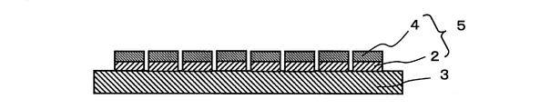
- the back surface of the semiconductor wafer 1 having at least one semiconductor circuit formed on the front surface that is, that is, The film-like adhesive of the present invention is thermocompression-bonded to the surface of the semiconductor wafer 1 on which the semiconductor circuit is not formed
- the dicing tape 3 is provided via the adhesive.
- the product in which the adhesive layer 2 and the dicing tape 3 are integrated may be thermocompression bonded to the back surface of the semiconductor wafer 1 at one time.
- the conditions for thermocompression bonding are such that the epoxy resin (A) is not substantially thermoset. For example, the conditions of 70 ° C.
- the semiconductor wafer 1 a semiconductor wafer having at least one semiconductor circuit formed on its surface can be appropriately used, and examples thereof include a silicon wafer, a SiC wafer, a GaAs wafer, and a GaN wafer.
- the adhesive layer 2 the film-like adhesive of the present invention may be used alone as one layer or may be used by laminating two or more layers.
- a method of providing such an adhesive layer 2 on the back surface of the wafer 1 a method capable of laminating a film-like adhesive on the back surface of the semiconductor wafer 1 can be appropriately adopted, and the method can be appropriately adopted on the back surface of the semiconductor wafer 1.
- a method of sequentially laminating the film-shaped adhesive until the desired thickness is obtained, or after laminating the film-shaped adhesive to the desired thickness in advance examples thereof include a method of bonding to the back surface of the semiconductor wafer 1.
- the device used when providing such an adhesive layer 2 on the back surface of the semiconductor wafer 1 is not particularly limited, and for example, a known device such as a roll laminator or a manual laminator can be appropriately used.
- the dicing tape 3 is not particularly limited, and a known dicing tape can be used as appropriate.
- the semiconductor wafer 1 semiconductor wafer 4
- the adhesive layer 2 are placed on the dicing tape 3.
- a semiconductor chip 5 with an adhesive layer comprising the above is obtained.
- the device used for dicing is not particularly limited, and a known dicing device can be used as appropriate.
- the dicing tape 3 is removed from the adhesive layer 2, and the semiconductor chip 5 with the adhesive layer and the wiring substrate 6 are thermocompression bonded via the adhesive layer 2.
- the semiconductor chip 5 with an adhesive layer is mounted on the wiring board 6.
- a substrate having a semiconductor circuit formed on its surface can be appropriately used.
- a printed circuit board (PCB) various lead frames, and electronic components such as resistance elements and capacitors are mounted on the surface of the substrate. The board is mentioned.
- a pick-up method using a normal jig can be adopted, specifically, a needle, a slider, or the like.
- a method of peeling from the dicing tape 3 with a jig can be mentioned.
- jig marks are less likely to occur on the surface of the film-like adhesive in this step.
- the method of mounting the semiconductor chip 5 with an adhesive layer on the wiring board 6 is not particularly limited, and the semiconductor chip 5 with an adhesive layer is mounted on the wiring board 6 or the surface of the wiring board 6 by using the adhesive layer 2.
- a conventional method capable of adhering to the electronic component is appropriately adopted.
- a mounting method conventionally known heating such as a method using a mounting technique using a flip-chip bonder having a heating function from the upper part, a method using a die bonder having a heating function only from the lower part, and a method using a laminator. , Pressurization method can be mentioned.
- the mounting (thermocompression bonding) conditions are such that the epoxy resin (A) is not substantially thermoset. For example, the conditions of 120 ° C., pressure of 0.1 MPa, and 1.0 second can be mentioned.
- the uneven portion on the wiring board 5 caused by the electronic components is formed. Since the film-like adhesive can be made to follow, the semiconductor chip 4 and the wiring substrate 6 can be brought into close contact with each other and fixed. According to the manufacturing method of the present invention, in this step, voids are less likely to occur at the interface between the adhesive layer made of a film-like adhesive and the wiring substrate, and mounting can be performed with high reliability.
- the adhesive layer 2 (the film-like adhesive of the present invention) is thermoset to obtain a thermosetting body.
- the thermosetting temperature is not particularly limited as long as it is equal to or higher than the thermosetting start temperature of the film-shaped adhesive of the present invention. It varies depending on the type and cannot be unconditionally stated, but for example, 100 to 180 ° C. is preferable, and 140 to 180 ° C. is more preferable from the viewpoint that curing at a higher temperature is possible in a short time. .. If the temperature is lower than the thermosetting start temperature, the thermosetting does not proceed sufficiently and the strength of the adhesive layer 2 tends to decrease.
- the curing treatment time is preferably, for example, 10 to 120 minutes.
- connection method is not particularly limited, and a conventionally known method, for example, a wire bonding method, a TAB (Tape Automated Bonding) method, or the like can be appropriately adopted.
- a plurality of semiconductor chips 4 can be laminated by thermocompression bonding, thermosetting, and reconnecting to the wiring board 6 by a wire bonding method on the surface of the mounted semiconductor chip 4. For example, a method of staggering and laminating semiconductor chips as shown in FIG. 5, or a method of laminating while embedding a bonding wire 7 by thickening the second and subsequent adhesive layers 2 as shown in FIG. be.
- the method for manufacturing a semiconductor package of the present invention as shown in FIG. 7, it is preferable to seal the wiring board 6 and the semiconductor chip 5 with an adhesive layer with a sealing resin 8, and thus the semiconductor package 9 is formed.
- the encapsulating resin 8 is not particularly limited, and an appropriately known encapsulating resin that can be used for manufacturing a semiconductor package can be used. Further, the sealing method using the sealing resin 8 is not particularly limited, and a known method can be appropriately adopted.
- the formation of jig marks in the pickup process can be suppressed even in the form of a thin film, and the generation of voids in the die attach process can be suppressed.
- room temperature means 25 ° C.
- MEK is methyl ethyl ketone
- PET is polyethylene terephthalate.
- Triphenylmethane type epoxy resin (trade name: EPPN-501H, mass average molecular weight: 1000, softening point: 55 ° C, semi-solid, epoxy equivalent: 167 g / eq, manufactured by Nippon Kayaku Co., Ltd.) 56 parts by mass, bisphenol A Type Epoxy resin (trade name: YD-128, mass average molecular weight: 400, softening point: 25 ° C or less, liquid, epoxy equivalent: 190 g / eq, manufactured by Shin Nikka Epoxy Manufacturing Co., Ltd.) 49 parts by mass, bisphenol A type Phenoxy resin (trade name: YP-50, mass average molecular weight: 70000, Tg: 84 ° C., room temperature (25 ° C.) elasticity: 1700 MPa, manufactured by Shin Nikka Epoxy Manufacturing Co., Ltd.) 30 parts by mass and 67 parts by mass of MEK 1000 ml A resin varnish was obtained by heating and stirring at a temperature of 110 ° C
- a film-like adhesive with a film was obtained.
- the obtained film-like adhesive was stored at 10 ° C. or lower. After the above drying, the epoxy resin has not been cured.
- Example 2 Alumina filler (trade name: AO-502, manufactured by Admatex Co., Ltd., average particle size (d50): 0.6 ⁇ m, Mohs hardness: 9 Mohs, thermal conductivity: 36 W / m ⁇ K) is used in an amount of 320 parts by mass.
- a film-like adhesive with a release film was produced in the same manner as in Example 1.
- Example 3 Alumina filler (trade name: AO-502, manufactured by Admatex Co., Ltd., average particle size (d50): 0.6 ⁇ m, Mohs hardness: 9 Mohs, thermal conductivity: 36 W / m ⁇ K) is used in an amount of 480 parts by mass.
- a film-like adhesive with a release film was produced in the same manner as in Example 1.
- Example 4 Replacing the phenoxy resin with a bisphenol A / F copolymerized phenoxy resin (trade name: YP-70, mass average molecular weight: 55000, Tg: 72 ° C., room temperature elasticity 1400 MPa, manufactured by Shin-Nippon Epoxy Manufacturing Co., Ltd.) A film-like adhesive with a release film was produced in the same manner as in Example 2 except for the above.
- Example 5 Except for replacing the phenoxy resin with a low elasticity and high heat resistant phenoxy resin (trade name: FX-310, mass average molecular weight: 40,000, Tg: 110 ° C, normal temperature elastic modulus 500 MPa, manufactured by Shin Nikka Epoxy Manufacturing Co., Ltd.) A film-like adhesive with a release film was produced in the same manner as in Example 2.
- Example 6 Bisphenol A type phenoxy resin (trade name: YP-50, mass average molecular weight: 70000, Tg: 84 ° C., normal temperature elastic modulus 1700 MPa, manufactured by Shin Nikka Epoxy Manufacturing Co., Ltd.) is used in 44 parts by mass, and the alumina filler is used. (Product name: AO-502, manufactured by Admatex Co., Ltd., average particle size (d50): 0.6 ⁇ m, moth hardness: 9 Mohs, thermal conductivity: 36 W / m ⁇ K) was used in an amount of 350 parts by mass. A film-like adhesive with a release film was produced in the same manner as in Example 1 except for the above.
- Example 7 Bisphenol A type phenoxy resin (trade name: YP-50, mass average molecular weight: 70000, Tg: 84 ° C., normal temperature elastic modulus 1700 MPa, manufactured by Shin Nikka Epoxy Manufacturing Co., Ltd.) is used in an amount of 70 parts by mass, and the alumina filler is used. (Product name: AO-502, manufactured by Admatex Co., Ltd., average particle size (d50): 0.6 ⁇ m, moth hardness: 9 Mohs, thermal conductivity: 36 W / m ⁇ K) was used in an amount of 400 parts by mass. A film-like adhesive with a release film was produced in the same manner as in Example 1 except for the above.
- Example 8 Bisphenol A type phenoxy resin (trade name: YP-50, mass average molecular weight: 70000, Tg: 84 ° C., normal temperature elastic modulus 1700 MPa, manufactured by Shin Nikka Epoxy Manufacturing Co., Ltd.) is used in an amount of 50 parts by mass and is filled with inorganic substances.
- Material is silver filler (trade name: AG-4-8F, manufactured by DOWA Electronics Co., Ltd., average particle size (d50): 2.0 ⁇ m, moth hardness: 2 Mohs, thermal conductivity: 429 W / m ⁇ K) 360 parts by mass
- a film-like adhesive with a release film was produced in the same manner as in Example 1 except that the adhesive was replaced with.
- Example 9 Bisphenol A type phenoxy resin (trade name: YP-50, mass average molecular weight: 70000, Tg: 84 ° C., normal temperature elastic modulus 1700 MPa, manufactured by Shin Nikka Epoxy Manufacturing Co., Ltd.) is used in an amount of 50 parts by mass and is filled with inorganic substances.
- Material is silver filler (trade name: AG-4-8F, manufactured by DOWA Electronics Co., Ltd., average particle size (d50): 2.0 ⁇ m, moth hardness: 2 Mohs, thermal conductivity: 429 W / m ⁇ K) 610 parts by mass.
- a film-like adhesive with a release film was produced in the same manner as in Example 1 except that the adhesive was replaced with.
- Example 10 Bisphenol A type phenoxy resin (trade name: YP-50, mass average molecular weight: 70000, Tg: 84 ° C., normal temperature elastic modulus 1700 MPa, manufactured by Shin Nikka Epoxy Manufacturing Co., Ltd.) is used in an amount of 50 parts by mass and is filled with inorganic substances.
- Material is silver filler (trade name: AG-4-8F, manufactured by DOWA Electronics Co., Ltd., average particle size (d50): 2.0 ⁇ m, moth hardness: 2 Mohs, thermal conductivity: 429 W / m ⁇ K) 950 parts by mass
- a film-like adhesive with a release film was produced in the same manner as in Example 1 except that the adhesive was replaced with.
- Example 11 Replace the inorganic filler with 14 parts by mass of silica filler (trade name: SO-25R, manufactured by SO-25R Co., Ltd., average particle size (d50): 0.5 ⁇ m, moth hardness: 7 Mohs, thermal conductivity: 1 W / m ⁇ K).
- silica filler trade name: SO-25R, manufactured by SO-25R Co., Ltd., average particle size (d50): 0.5 ⁇ m, moth hardness: 7 Mohs, thermal conductivity: 1 W / m ⁇ K.
- Example 12 Replace the inorganic filler with 67 parts by mass of silica filler (trade name: SO-25R, manufactured by SO-25R, average particle size (d50): 0.5 ⁇ m, moth hardness: 7 Mohs, thermal conductivity: 1 W / m ⁇ K).
- silica filler trade name: SO-25R, manufactured by SO-25R, average particle size (d50): 0.5 ⁇ m, moth hardness: 7 Mohs, thermal conductivity: 1 W / m ⁇ K.
- Example 13 Replaced the inorganic filler with 14 parts by mass of nanosilica filler (trade name: RY-200, manufactured by Nippon Aerosil Co., Ltd., average particle size (d50): 12 nm, moth hardness: 7 Mohs, thermal conductivity: 1 W / m ⁇ K).
- nanosilica filler trade name: RY-200, manufactured by Nippon Aerosil Co., Ltd., average particle size (d50): 12 nm, moth hardness: 7 Mohs, thermal conductivity: 1 W / m ⁇ K.
- Example 14 Replaced the inorganic filler with 67 parts by mass of nanosilica filler (trade name: RY-200, manufactured by Nippon Aerosil Co., Ltd., average particle size (d50): 12 nm, moth hardness: 7 Mohs, thermal conductivity: 1 W / m ⁇ K).
- nanosilica filler trade name: RY-200, manufactured by Nippon Aerosil Co., Ltd., average particle size (d50): 12 nm, moth hardness: 7 Mohs, thermal conductivity: 1 W / m ⁇ K.
- Example 15 Except for the fact that the amount of bisphenol A type phenoxy resin (trade name: YP-50, mass average molecular weight: 70000, Tg: 84 ° C., normal temperature elastic modulus 1700 MPa, manufactured by Shin Nikka Epoxy Manufacturing Co., Ltd.) was set to 15 parts by mass. Made a film-like adhesive in the same manner as in Example 1.
- bisphenol A type phenoxy resin trade name: YP-50, mass average molecular weight: 70000, Tg: 84 ° C., normal temperature elastic modulus 1700 MPa, manufactured by Shin Nikka Epoxy Manufacturing Co., Ltd.
- Example 16 Except for the fact that the amount of bisphenol A type phenoxy resin (trade name: YP-50, mass average molecular weight: 70000, Tg: 84 ° C., normal temperature elastic modulus 1700 MPa, manufactured by Shin Nikka Epoxy Manufacturing Co., Ltd.) was set to 130 parts by mass. Made a film-like adhesive in the same manner as in Example 1.
- bisphenol A type phenoxy resin trade name: YP-50, mass average molecular weight: 70000, Tg: 84 ° C., normal temperature elastic modulus 1700 MPa, manufactured by Shin Nikka Epoxy Manufacturing Co., Ltd.
- Example 17 Silica filler whose particle size distribution is adjusted using a 10.0 ⁇ m mesh filter for the inorganic filler (trade name: FB-7SDS, DENKA Co., Ltd., average particle size (d50): 5.4 ⁇ m, moth hardness: 7Mohs, thermal conductivity Rate: 1 W / m ⁇ K)
- a film-like adhesive was produced in the same manner as in Example 1 except that it was replaced with 30 parts by mass.
- Phenoxy resin is bisphenol F + 1,6-hexanediol diglycidyl ether type phenoxy resin (trade name: YX-7180, mass average molecular weight: 50,000, Tg: 15 ° C., room temperature elasticity 200 MPa, manufactured by Mitsubishi Chemical Co., Ltd.) 10 parts by mass Instead, use an alumina filler (trade name: AO-502, manufactured by Admatex Co., Ltd., average particle size (d50): 0.6 ⁇ m, moth hardness: 9 Mohs, thermal conductivity: 36 W / m ⁇ K).
- a film-like adhesive with a release film was produced in the same manner as in Example 1 except that the amount was 275 parts by mass.
- Phenoxy resin is bisphenol F + 1,6-hexanediol diglycidyl ether type phenoxy resin (trade name: YX-7180, mass average molecular weight: 50,000, Tg: 15 ° C., room temperature elasticity 200 MPa, manufactured by Mitsubishi Chemical Co., Ltd.) 190 parts by mass Instead, use an alumina filler (trade name: AO-502, manufactured by Admatex Co., Ltd., average particle size (d50): 0.6 ⁇ m, moth hardness: 9 Mohs, thermal conductivity: 36 W / m ⁇ K).
- a film-like adhesive with a release film was produced in the same manner as in Example 1 except that the amount was 670 parts by mass.
- Phenoxy resin is bisphenol F + 1,6-hexanediol diglycidyl ether type phenoxy resin (trade name: YX-7180, mass average molecular weight: 50,000, Tg: 15 ° C., room temperature elasticity 200 MPa, manufactured by Mitsubishi Chemical Corporation) 30 parts by mass.
- a film-like adhesive was produced in the same manner as in Example 1 except that the adhesive was replaced with.
- Epoxy resin is a triphenylmethane type epoxy resin (trade name: EPPN-501H, mass average molecular weight: 1000, softening point: 55 ° C., semi-solid, epoxy equivalent: 167 g / eq, manufactured by Nippon Kayaku Co., Ltd.) 50 parts by mass
- the amount of bisphenol A type phenoxy resin (trade name: YP-50, mass average molecular weight: 70000, Tg: 84 ° C., room temperature elasticity 1700 MPa, manufactured by Shin Nikka Epoxy Manufacturing Co., Ltd.) was set to 100 parts by mass.
- Alumina filler (trade name: AO-502, manufactured by Admatex Co., Ltd., average particle size (d50): 0.6 ⁇ m, moth hardness: 9 Mohs, thermal conductivity: 36 W / m ⁇ K) is used in an amount of 450 parts by mass.
- a film-like adhesive with a release film was produced in the same manner as in Example 1 except that the amount of the silane coupling agent (trade name: Sila Ace S-510, manufactured by JNC Co., Ltd.) was 7.0 parts by mass. did.
- Silicone filler for inorganic filler (trade name: MSP-SN05, manufactured by Nikko Rika Co., Ltd., average particle size (d50): 0.5 ⁇ m, moth hardness: 1 Mohs or less, thermal conductivity: 0.2 W / m ⁇ K)
- a film-like adhesive with a release film was produced in the same manner as in Example 1 except that the amount was 8 parts by mass.
- Silicone filler for inorganic filler (trade name: MSP-SN05, manufactured by Nikko Rika Co., Ltd., average particle size (d50): 0.5 ⁇ m, moth hardness: 1 Mohs or less, thermal conductivity: 0.2 W / m ⁇ K)
- a film-like adhesive with a release film was produced in the same manner as in Example 1 except that the amount was 95 parts by mass.
- Silicone filler for inorganic filler (trade name: MSP-SN05, manufactured by Nikko Rika Co., Ltd., average particle size (d50): 0.5 ⁇ m, moth hardness: 1 Mohs or less, thermal conductivity: 0.2 W / m ⁇ K)
- a film-like adhesive with a release film was produced in the same manner as in Example 1 except that the amount was 220 parts by mass.
- the elastic modulus of the phenoxy resin and the acrylic resin used in each Example and Comparative Example at 25 ° C. was measured as follows. ⁇ Normal temperature (25 ° C) elastic modulus> 30 parts by mass of various phenoxy resins and 70 parts by mass of MEK (methyl ethyl ketone) were heated and stirred in a 500 ml separable flask at a temperature of 110 ° C. for 2 hours to obtain a resin varnish. Next, this resin varnish was applied onto a PET film (release film) having a thickness of 38 ⁇ m and subjected to a mold release treatment, and dried by heating at 130 ° C. for 10 minutes.
- This phenoxy resin film is cut into a size of 5 mm ⁇ 17 mm, and a dynamic viscoelasticity measuring device (trade name: Rheogel-E4000F, manufactured by UBM Co., Ltd.) is used to measure a temperature range of 0 to 100 ° C. and a temperature rise rate of 5. The measurement was carried out under the conditions of ° C./min and a frequency of 1 Hz, and the value of the elastic modulus at 25 ° C. was determined. As with the phenoxy resin, the elastic modulus of the acrylic resin at 25 ° C. was determined according to the above method.
- the average particle size (d50) of the inorganic filler used in each Example and Comparative Example was measured as follows. ⁇ Measurement of average particle size (d50)> 0.1 g of each inorganic filler used above and 9.9 g of MEK were weighed, and a mixture thereof was subjected to ultrasonic dispersion treatment for 5 minutes to prepare a sample for measurement. For this measurement sample, the average particle size (d50) was obtained from the cumulative curve of the volume fraction of the particle size distribution measured by the laser diffraction / scattering method (model: LMS-2000e, manufactured by Seishin Co., Ltd.). rice field.
- a triangular pyramid diamond indenter (Berkovich type; 115 °) was pushed from the surface of the film-like adhesive at a loading time of 80 seconds, a waiting time of 17 seconds, and an unloading time of 80 seconds, and measurements were carried out. Young's modulus and nanoindentation hardness were determined from the Poisson's ratio of each sample. Although the test pieces are bonded at 70 ° C. when prepared, the epoxy resin does not substantially undergo a curing reaction even when exposed to 70 ° C. for the above short time. Therefore, the above measurement result is substantially the same as the result using the film-like adhesive which has not been exposed to the temperature of 25 ° C. or higher.
- melt viscosity From the film-like adhesive with a release film obtained in each Example and Comparative Example, a square having a size of 5.0 cm in length ⁇ 5.0 cm in width was cut out, and the sample cut out with the release film peeled off was laminated and laminated at 70 ° C. A test piece having a thickness of about 1.0 mm was obtained by laminating with a hand roller on the stage of. For this test piece, a rheometer (RS6000, manufactured by Hake) was used to measure the change in viscous resistance in a temperature range of 20 to 250 ° C. and a heating rate of 5 ° C./min. From the obtained temperature-viscosity resistance curve, the melt viscosity (Pa ⁇ s) at 120 ° C. was calculated.
- RS6000 rheometer
- the film-like adhesive with a release film obtained in each Example and Comparative Example was subjected to dummy silicon at a temperature of 70 ° C. and a pressure of 0.3 MPa using a manual laminator (trade name: FM-114, manufactured by Technovision Co., Ltd.). It was adhered to one surface of a wafer (8 inch size, thickness 100 ⁇ m). Then, after peeling the release film from the film-like adhesive, a dicing tape (trade name:) is used on the surface of the film-like adhesive on the surface opposite to the dummy silicon wafer at room temperature and pressure of 0.3 MPa using the same manual laminator.
- a manual laminator trade name: FM-114, manufactured by Technovision Co., Ltd.
- dicing frame (trade name: DTF2-8-1H001, manufactured by DISCO) were adhered.
- a dicing device (trade name: DFD-6340, manufactured by DISCO) equipped with a two-axis dicing blade (Z1: NBC-ZH2050 (27HEDD), Z2: NBC-ZH127F-SE (BC), DISCO). Dicing was performed from the dummy silicon wafer side so as to have a size of 5 mm ⁇ 5 mm using DISCO) to obtain a dummy chip with a film-like adhesive.
- a die bonder (trade name: DB-800, manufactured by Hitachi High-Technologies Corporation) picks up the dummy chip with a film-like adhesive from the dicing tape under the following conditions, and puts it on the film-like adhesive after pickup. The state of the needle mark was observed, and the needle mark was evaluated by the following evaluation. In this test, evaluation ranks "AA" and "A” are pass levels. Pickup conditions 4 needles, needle R150 ( ⁇ m), needle pitch 3.5 mm, push-up speed 5 mm / sec, push-up height 200 ⁇ m, pick-up time 100 msec Evaluation criteria AA: Film-like in all 24 picked-up semiconductor chips No needle marks are observed on the adhesive surface.
- Needle marks were observed on the surface of the film-like adhesive in 1 to 3 of the 24 semiconductor chips picked up, and the number of needle marks on the surface of the film-like adhesive in which the needle marks were observed was 1 to 3.
- Is. B Needle marks are observed on the surface of the film-like adhesive in 1 to 3 of the 24 semiconductor chips picked up, and the number of needle marks on the surface of the film-like adhesive in which the needle marks are observed is 4. .. C: Needle marks are observed on the surface of the film-like adhesive in 4 or more of the 24 semiconductor chips picked up.
- the film-like adhesive with a release film obtained in each Example and Comparative Example was subjected to dummy silicon at a temperature of 70 ° C. and a pressure of 0.3 MPa using a manual laminator (trade name: FM-114, manufactured by Technovision Co., Ltd.). It was adhered to one surface of a wafer (8 inch size, thickness 100 ⁇ m). Then, after peeling the release film from the film-like adhesive, a dicing tape (trade name:) is used on the surface of the film-like adhesive on the surface opposite to the dummy silicon wafer at room temperature and pressure of 0.3 MPa using the same manual laminator.
- a manual laminator trade name: FM-114, manufactured by Technovision Co., Ltd.
- dicing frame (trade name: DTF2-8-1H001, manufactured by DISCO) were adhered.
- a dicing device (trade name: DFD-6340, manufactured by DISCO) equipped with a two-axis dicing blade (Z1: NBC-ZH2050 (27HEDD), Z2: NBC-ZH127F-SE (BC), DISCO). Dicing was performed from the dummy silicon wafer side so as to have a size of 10 mm ⁇ 10 mm using DISCO) to obtain a dummy chip with a film-like adhesive.
- the dummy chip with a film-like adhesive was picked up from the dicing tape by a die bonder (trade name: DB-800, manufactured by Hitachi High-Technologies Co., Ltd.), 120 ° C., pressure 0.1 MPa (load 400 gf), time. Under the condition of 1.0 second, heat is applied so that the film-like adhesive side of the dummy chip with the film-like adhesive and the mounting surface side of the lead frame substrate (42 Alloy system, manufactured by Letterpress Printing Co., Ltd.) are bonded together. It was crimped.
- the mounting surface of the lead frame substrate is a metal surface having a slight surface roughness.
- the film-like adhesives obtained by using the adhesive compositions that do not satisfy any of the composition, the ratio of the phenoxy resin, the Young's modulus, and the nanoindentation hardness specified in the present invention are all used for needle mark evaluation and needle mark evaluation.
- One of the die attachability evaluations failed, and the suppression of jig marks and the improvement of the die attachability could not be achieved.
- the film-like adhesives obtained by using the adhesive compositions of Examples 1 to 17 of the present invention did not easily leave jig marks and were excellent in die attachability.
Landscapes
- Chemical & Material Sciences (AREA)
- Organic Chemistry (AREA)
- Inorganic Chemistry (AREA)
- Chemical Kinetics & Catalysis (AREA)
- Medicinal Chemistry (AREA)
- Polymers & Plastics (AREA)
- Health & Medical Sciences (AREA)
- Life Sciences & Earth Sciences (AREA)
- Engineering & Computer Science (AREA)
- Materials Engineering (AREA)
- Wood Science & Technology (AREA)
- Adhesives Or Adhesive Processes (AREA)
- Adhesive Tapes (AREA)
- Die Bonding (AREA)
- Dicing (AREA)
Priority Applications (5)
| Application Number | Priority Date | Filing Date | Title |
|---|---|---|---|
| MYPI2022005764A MY202084A (en) | 2020-07-30 | 2021-05-19 | Adhesive composition and film-like adhesive, and semiconductor package using film-like adhesive and producing method thereof |
| CN202180030059.3A CN115461423B (zh) | 2020-07-30 | 2021-05-19 | 粘接剂用组合物和膜状粘接剂、以及使用了膜状粘接剂的半导体封装及其制造方法 |
| KR1020227036608A KR102655890B1 (ko) | 2020-07-30 | 2021-05-19 | 접착제용 조성물 및 필름형 접착제와 필름형 접착제를 사용한 반도체 패키지 및 그 제조 방법 |
| JP2021552639A JP7042986B1 (ja) | 2020-07-30 | 2021-05-19 | 接着剤用組成物及びフィルム状接着剤、並びに、フィルム状接着剤を用いた半導体パッケージ及びその製造方法 |
| US17/970,402 US20230108567A1 (en) | 2020-07-30 | 2022-10-20 | Adhesive composition and film-like adhesive, and semiconductor package using film-like adhesive and producing method thereof |
Applications Claiming Priority (2)
| Application Number | Priority Date | Filing Date | Title |
|---|---|---|---|
| JP2020-129493 | 2020-07-30 | ||
| JP2020129493 | 2020-07-30 |
Related Child Applications (1)
| Application Number | Title | Priority Date | Filing Date |
|---|---|---|---|
| US17/970,402 Continuation US20230108567A1 (en) | 2020-07-30 | 2022-10-20 | Adhesive composition and film-like adhesive, and semiconductor package using film-like adhesive and producing method thereof |
Publications (1)
| Publication Number | Publication Date |
|---|---|
| WO2022024510A1 true WO2022024510A1 (ja) | 2022-02-03 |
Family
ID=80037969
Family Applications (1)
| Application Number | Title | Priority Date | Filing Date |
|---|---|---|---|
| PCT/JP2021/018947 Ceased WO2022024510A1 (ja) | 2020-07-30 | 2021-05-19 | 接着剤用組成物及びフィルム状接着剤、並びに、フィルム状接着剤を用いた半導体パッケージ及びその製造方法 |
Country Status (7)
| Country | Link |
|---|---|
| US (1) | US20230108567A1 (https=) |
| JP (1) | JP7042986B1 (https=) |
| KR (1) | KR102655890B1 (https=) |
| CN (1) | CN115461423B (https=) |
| MY (1) | MY202084A (https=) |
| TW (1) | TWI843947B (https=) |
| WO (1) | WO2022024510A1 (https=) |
Cited By (3)
| Publication number | Priority date | Publication date | Assignee | Title |
|---|---|---|---|---|
| KR20230158517A (ko) * | 2022-03-30 | 2023-11-20 | 후루카와 덴키 고교 가부시키가이샤 | 열 전도성 필름형 접착제용 조성물 및 열 전도성 필름형 접착제, 그리고 열 전도성 필름형 접착제를 사용한 반도체 패키지 및 그 제조 방법 |
| WO2025013945A1 (ja) * | 2023-07-12 | 2025-01-16 | 日東シンコー株式会社 | セラミックシート及び半導体装置 |
| WO2025204162A1 (ja) * | 2024-03-26 | 2025-10-02 | ナミックス株式会社 | 樹脂組成物、それを用いた熱硬化性フィルム、熱硬化性フィルムの硬化物、及び半導体装置 |
Citations (11)
| Publication number | Priority date | Publication date | Assignee | Title |
|---|---|---|---|---|
| JP2008124141A (ja) * | 2006-11-09 | 2008-05-29 | Shin Etsu Chem Co Ltd | ダイシング・ダイボンド用接着フィルム |
| JP2009167372A (ja) * | 2008-01-21 | 2009-07-30 | Sekisui Chem Co Ltd | 電気部品用接着剤 |
| JP2012049388A (ja) * | 2010-08-27 | 2012-03-08 | Shin Etsu Chem Co Ltd | 半導体ウエハ保護膜形成用シート |
| WO2013161864A1 (ja) * | 2012-04-26 | 2013-10-31 | 新日鉄住金化学株式会社 | フィルム状接着剤用組成物及びその製造方法、フィルム状接着剤、並びに、フィルム状接着剤を用いた半導体パッケージ及びその製造方法 |
| JP2016065209A (ja) * | 2014-09-25 | 2016-04-28 | 日東電工株式会社 | 熱剥離型粘着シート |
| JP2017183642A (ja) * | 2016-03-31 | 2017-10-05 | 古河電気工業株式会社 | 電子デバイスパッケージ用テープ |
| JP2017179055A (ja) * | 2016-03-29 | 2017-10-05 | 味の素株式会社 | 熱硬化性樹脂組成物 |
| WO2017168820A1 (ja) * | 2016-03-31 | 2017-10-05 | 古河電気工業株式会社 | 電子デバイスパッケージ用テープ |
| JP2018182276A (ja) * | 2017-04-17 | 2018-11-15 | 日東電工株式会社 | ダイシングダイボンドフィルム |
| JP2018188540A (ja) * | 2017-05-01 | 2018-11-29 | 古河電気工業株式会社 | 接着フィルム、半導体ウェハ加工用テープ、半導体パッケージおよびその製造方法 |
| JP2020061423A (ja) * | 2018-10-05 | 2020-04-16 | 日東電工株式会社 | ダイシングダイボンドフィルム |
Family Cites Families (7)
| Publication number | Priority date | Publication date | Assignee | Title |
|---|---|---|---|---|
| JPS5322609U (https=) | 1976-08-05 | 1978-02-25 | ||
| JP4421422B2 (ja) | 2004-08-20 | 2010-02-24 | 信越化学工業株式会社 | ダイアタッチ可能な半導体チップの製造方法 |
| JP5871428B2 (ja) * | 2011-03-16 | 2016-03-01 | 古河電気工業株式会社 | 高熱伝導性フィルム状接着剤用組成物、高熱伝導性フィルム状接着剤、並びに、それを用いた半導体パッケージとその製造方法 |
| KR20180116756A (ko) * | 2017-04-17 | 2018-10-25 | 닛토덴코 가부시키가이샤 | 다이싱 다이 본드 필름 |
| JP6889398B2 (ja) | 2017-07-20 | 2021-06-18 | 昭和電工マテリアルズ株式会社 | 放熱性ダイボンディングフィルム及びダイシングダイボンディングフィルム |
| JP6800129B2 (ja) * | 2017-11-07 | 2020-12-16 | 古河電気工業株式会社 | フィルム状接着剤、フィルム状接着剤を用いた半導体パッケージの製造方法 |
| CN116601250A (zh) * | 2020-12-25 | 2023-08-15 | 株式会社力森诺科 | 电路连接用黏合剂膜、以及电路连接结构体及其制造方法 |
-
2021
- 2021-05-19 KR KR1020227036608A patent/KR102655890B1/ko active Active
- 2021-05-19 CN CN202180030059.3A patent/CN115461423B/zh active Active
- 2021-05-19 WO PCT/JP2021/018947 patent/WO2022024510A1/ja not_active Ceased
- 2021-05-19 MY MYPI2022005764A patent/MY202084A/en unknown
- 2021-05-19 JP JP2021552639A patent/JP7042986B1/ja active Active
- 2021-05-21 TW TW110118462A patent/TWI843947B/zh active
-
2022
- 2022-10-20 US US17/970,402 patent/US20230108567A1/en active Pending
Patent Citations (11)
| Publication number | Priority date | Publication date | Assignee | Title |
|---|---|---|---|---|
| JP2008124141A (ja) * | 2006-11-09 | 2008-05-29 | Shin Etsu Chem Co Ltd | ダイシング・ダイボンド用接着フィルム |
| JP2009167372A (ja) * | 2008-01-21 | 2009-07-30 | Sekisui Chem Co Ltd | 電気部品用接着剤 |
| JP2012049388A (ja) * | 2010-08-27 | 2012-03-08 | Shin Etsu Chem Co Ltd | 半導体ウエハ保護膜形成用シート |
| WO2013161864A1 (ja) * | 2012-04-26 | 2013-10-31 | 新日鉄住金化学株式会社 | フィルム状接着剤用組成物及びその製造方法、フィルム状接着剤、並びに、フィルム状接着剤を用いた半導体パッケージ及びその製造方法 |
| JP2016065209A (ja) * | 2014-09-25 | 2016-04-28 | 日東電工株式会社 | 熱剥離型粘着シート |
| JP2017179055A (ja) * | 2016-03-29 | 2017-10-05 | 味の素株式会社 | 熱硬化性樹脂組成物 |
| JP2017183642A (ja) * | 2016-03-31 | 2017-10-05 | 古河電気工業株式会社 | 電子デバイスパッケージ用テープ |
| WO2017168820A1 (ja) * | 2016-03-31 | 2017-10-05 | 古河電気工業株式会社 | 電子デバイスパッケージ用テープ |
| JP2018182276A (ja) * | 2017-04-17 | 2018-11-15 | 日東電工株式会社 | ダイシングダイボンドフィルム |
| JP2018188540A (ja) * | 2017-05-01 | 2018-11-29 | 古河電気工業株式会社 | 接着フィルム、半導体ウェハ加工用テープ、半導体パッケージおよびその製造方法 |
| JP2020061423A (ja) * | 2018-10-05 | 2020-04-16 | 日東電工株式会社 | ダイシングダイボンドフィルム |
Cited By (4)
| Publication number | Priority date | Publication date | Assignee | Title |
|---|---|---|---|---|
| KR20230158517A (ko) * | 2022-03-30 | 2023-11-20 | 후루카와 덴키 고교 가부시키가이샤 | 열 전도성 필름형 접착제용 조성물 및 열 전도성 필름형 접착제, 그리고 열 전도성 필름형 접착제를 사용한 반도체 패키지 및 그 제조 방법 |
| KR102742635B1 (ko) | 2022-03-30 | 2024-12-17 | 후루카와 덴키 고교 가부시키가이샤 | 열 전도성 필름형 접착제용 조성물 및 열 전도성 필름형 접착제, 그리고 열 전도성 필름형 접착제를 사용한 반도체 패키지 및 그 제조 방법 |
| WO2025013945A1 (ja) * | 2023-07-12 | 2025-01-16 | 日東シンコー株式会社 | セラミックシート及び半導体装置 |
| WO2025204162A1 (ja) * | 2024-03-26 | 2025-10-02 | ナミックス株式会社 | 樹脂組成物、それを用いた熱硬化性フィルム、熱硬化性フィルムの硬化物、及び半導体装置 |
Also Published As
| Publication number | Publication date |
|---|---|
| CN115461423B (zh) | 2024-07-05 |
| US20230108567A1 (en) | 2023-04-06 |
| TWI843947B (zh) | 2024-06-01 |
| JPWO2022024510A1 (https=) | 2022-02-03 |
| MY202084A (en) | 2024-04-03 |
| CN115461423A (zh) | 2022-12-09 |
| JP7042986B1 (ja) | 2022-03-28 |
| TW202204558A (zh) | 2022-02-01 |
| KR20230046274A (ko) | 2023-04-05 |
| KR102655890B1 (ko) | 2024-04-11 |
Similar Documents
| Publication | Publication Date | Title |
|---|---|---|
| US11952513B2 (en) | Adhesive composition, film-like adhesive and production method thereof, and semiconductor package using film-like adhesive and production method thereof | |
| JP7178529B1 (ja) | 熱伝導性フィルム状接着剤、半導体パッケージ及びその製造方法 | |
| JP6902641B1 (ja) | ダイシングダイアタッチフィルム、並びに、ダイシングダイアタッチフィルムを用いた半導体パッケージ及びその製造方法 | |
| US20230108567A1 (en) | Adhesive composition and film-like adhesive, and semiconductor package using film-like adhesive and producing method thereof | |
| JP6989721B1 (ja) | ダイシングダイアタッチフィルム及びその製造方法、並びに半導体パッケージ及びその製造方法 | |
| KR102683506B1 (ko) | 접착제용 조성물 및 필름형 접착제와 필름형 접착제를 사용한 반도체 패키지 및 그 제조 방법 | |
| KR102779253B1 (ko) | 접착제용 조성물 및 필름형 접착제, 그리고 필름형 접착제를 사용한 반도체 패키지 및 그 제조 방법 | |
| HK40077351B (zh) | 粘接剂用组合物和膜状粘接剂、以及使用了膜状粘接剂的半导体封装及其制造方法 | |
| HK40077351A (en) | Composition for adhesive, film-like adhesive, and semiconductor package in which film-like adhesive is used and method for manufacturing same | |
| WO2023286389A1 (ja) | 熱伝導性フィルム状接着剤、半導体パッケージ及びその製造方法 | |
| WO2025205832A1 (ja) | フィルム状接着剤、接着剤用組成物、ダイシング・ダイアタッチフィルム、並びに半導体パッケージ及び半導体パッケージの製造方法 | |
| HK40059508B (zh) | 切晶粘晶膜、以及使用了该切晶粘晶膜的半导体封装及其制造方法 |
Legal Events
| Date | Code | Title | Description |
|---|---|---|---|
| ENP | Entry into the national phase |
Ref document number: 2021552639 Country of ref document: JP Kind code of ref document: A |
|
| 121 | Ep: the epo has been informed by wipo that ep was designated in this application |
Ref document number: 21850819 Country of ref document: EP Kind code of ref document: A1 |
|
| NENP | Non-entry into the national phase |
Ref country code: DE |
|
| 122 | Ep: pct application non-entry in european phase |
Ref document number: 21850819 Country of ref document: EP Kind code of ref document: A1 |