WO2022019112A1 - フィルタ装置およびそれを備える高周波フロントエンド回路 - Google Patents
フィルタ装置およびそれを備える高周波フロントエンド回路 Download PDFInfo
- Publication number
- WO2022019112A1 WO2022019112A1 PCT/JP2021/025591 JP2021025591W WO2022019112A1 WO 2022019112 A1 WO2022019112 A1 WO 2022019112A1 JP 2021025591 W JP2021025591 W JP 2021025591W WO 2022019112 A1 WO2022019112 A1 WO 2022019112A1
- Authority
- WO
- WIPO (PCT)
- Prior art keywords
- parallel resonator
- common electrode
- resonator
- filter device
- capacitor
- Prior art date
- Legal status (The legal status is an assumption and is not a legal conclusion. Google has not performed a legal analysis and makes no representation as to the accuracy of the status listed.)
- Ceased
Links
Images












Classifications
-
- H—ELECTRICITY
- H01—ELECTRIC ELEMENTS
- H01F—MAGNETS; INDUCTANCES; TRANSFORMERS; SELECTION OF MATERIALS FOR THEIR MAGNETIC PROPERTIES
- H01F17/00—Fixed inductances of the signal type
- H01F17/0006—Printed inductances
- H01F17/0013—Printed inductances with stacked layers
-
- H—ELECTRICITY
- H01—ELECTRIC ELEMENTS
- H01F—MAGNETS; INDUCTANCES; TRANSFORMERS; SELECTION OF MATERIALS FOR THEIR MAGNETIC PROPERTIES
- H01F27/00—Details of transformers or inductances, in general
- H01F27/28—Coils; Windings; Conductive connections
- H01F27/2804—Printed windings
-
- H—ELECTRICITY
- H01—ELECTRIC ELEMENTS
- H01G—CAPACITORS; CAPACITORS, RECTIFIERS, DETECTORS, SWITCHING DEVICES, LIGHT-SENSITIVE OR TEMPERATURE-SENSITIVE DEVICES OF THE ELECTROLYTIC TYPE
- H01G4/00—Fixed capacitors; Processes of their manufacture
- H01G4/30—Stacked capacitors
-
- H—ELECTRICITY
- H01—ELECTRIC ELEMENTS
- H01G—CAPACITORS; CAPACITORS, RECTIFIERS, DETECTORS, SWITCHING DEVICES, LIGHT-SENSITIVE OR TEMPERATURE-SENSITIVE DEVICES OF THE ELECTROLYTIC TYPE
- H01G4/00—Fixed capacitors; Processes of their manufacture
- H01G4/40—Structural combinations of fixed capacitors with other electric elements, the structure mainly consisting of a capacitor, e.g. RC combinations
-
- H—ELECTRICITY
- H01—ELECTRIC ELEMENTS
- H01P—WAVEGUIDES; RESONATORS, LINES, OR OTHER DEVICES OF THE WAVEGUIDE TYPE
- H01P1/00—Auxiliary devices
- H01P1/20—Frequency-selective devices, e.g. filters
- H01P1/201—Filters for transverse electromagnetic waves
- H01P1/203—Strip line filters
- H01P1/20327—Electromagnetic interstage coupling
- H01P1/20354—Non-comb or non-interdigital filters
- H01P1/20381—Special shape resonators
-
- H—ELECTRICITY
- H03—ELECTRONIC CIRCUITRY
- H03H—IMPEDANCE NETWORKS, e.g. RESONANT CIRCUITS; RESONATORS
- H03H7/00—Multiple-port networks comprising only passive electrical elements as network components
- H03H7/01—Frequency selective two-port networks
- H03H7/0115—Frequency selective two-port networks comprising only inductors and capacitors
-
- H—ELECTRICITY
- H03—ELECTRONIC CIRCUITRY
- H03H—IMPEDANCE NETWORKS, e.g. RESONANT CIRCUITS; RESONATORS
- H03H7/00—Multiple-port networks comprising only passive electrical elements as network components
- H03H7/01—Frequency selective two-port networks
- H03H7/17—Structural details of sub-circuits of frequency selective networks
- H03H7/1708—Comprising bridging elements, i.e. elements in a series path without own reference to ground and spanning branching nodes of another series path
-
- H—ELECTRICITY
- H03—ELECTRONIC CIRCUITRY
- H03H—IMPEDANCE NETWORKS, e.g. RESONANT CIRCUITS; RESONATORS
- H03H7/00—Multiple-port networks comprising only passive electrical elements as network components
- H03H7/01—Frequency selective two-port networks
- H03H7/17—Structural details of sub-circuits of frequency selective networks
- H03H7/1741—Comprising typical LC combinations, irrespective of presence and location of additional resistors
- H03H7/1775—Parallel LC in shunt or branch path
-
- H—ELECTRICITY
- H01—ELECTRIC ELEMENTS
- H01F—MAGNETS; INDUCTANCES; TRANSFORMERS; SELECTION OF MATERIALS FOR THEIR MAGNETIC PROPERTIES
- H01F17/00—Fixed inductances of the signal type
- H01F17/0006—Printed inductances
- H01F17/0013—Printed inductances with stacked layers
- H01F2017/0026—Multilayer LC-filter
-
- H—ELECTRICITY
- H01—ELECTRIC ELEMENTS
- H01F—MAGNETS; INDUCTANCES; TRANSFORMERS; SELECTION OF MATERIALS FOR THEIR MAGNETIC PROPERTIES
- H01F27/00—Details of transformers or inductances, in general
- H01F27/28—Coils; Windings; Conductive connections
- H01F27/2804—Printed windings
- H01F2027/2809—Printed windings on stacked layers
-
- H—ELECTRICITY
- H03—ELECTRONIC CIRCUITRY
- H03H—IMPEDANCE NETWORKS, e.g. RESONANT CIRCUITS; RESONATORS
- H03H1/00—Constructional details of impedance networks whose electrical mode of operation is not specified or applicable to more than one type of network
- H03H2001/0021—Constructional details
- H03H2001/0085—Multilayer, e.g. LTCC, HTCC, green sheets
Definitions
- the present disclosure relates to a filter device and a high frequency front-end circuit including the filter device, and more specifically, to a technique for improving the characteristics of a laminated LC filter.
- Patent Document 1 discloses a laminated bandpass filter in which a four-stage LC parallel resonator is arranged between an input terminal and an output terminal.
- the bandpass filter of International Publication No. 2019/097744 Patent Document 1
- two capacitors first
- a capacitor capacitor, second capacitor
- a third capacitor is formed between the connection node of the two capacitors and the grounding point.
- the inductors that form each LC parallel resonator included in the bandpass filter of International Publication No. 2019/097744 include two via conductors formed in the stacking direction of the dielectric substrate having a multilayer structure and the said one. It is formed by line conductors connecting via conductors, and the line conductors of each LC parallel resonator are arranged apart from each other.
- it is generally performed by changing the position (interval) of the via conductor forming the inductor or changing the spacing between the resonators. ..
- the Q value may decrease because the air core diameter of the inductor changes. Further, when the distance between specific resonators is changed, the magnetic coupling with other resonators is also affected, and the loss may be rather large.
- the bandpass filter as described above may be used in a portable communication device represented by a mobile phone or a smartphone.
- a mobile terminal further miniaturization and thinning are required, but if the filter is miniaturized accordingly, the degree of freedom in the arrangement of the via conductor is further limited, so that the space between the resonators is further limited. Adjustment of magnetic coupling can be difficult.
- the present disclosure has been made to solve such a problem, and an object thereof is a resonator in a multi-stage laminated filter including a plurality of LC parallel resonators while suppressing a decrease in Q value. It is to adjust the magnetic coupling between them.
- the filter device includes an input terminal, an output terminal, a main body, a common electrode provided in the main body, a ground terminal, and first to third LC parallel resonators connected to the common electrode and the ground terminal.
- Each resonator includes a capacitor, a first via, and a second via.
- One end of the first via is connected to a common electrode, and the other end is connected to a ground terminal via a capacitor.
- One end of the second via is connected to a common electrode, and the other end is connected to a ground terminal without a capacitor.
- the second via is connected between the portions of the common electrode to which the first vias of two adjacent resonators are connected.
- a plurality of LC parallel resonators (first LC parallel resonator to third LC parallel resonator) magnetically coupled to each other are connected by a common electrode.
- the arrangement of vias constituting the inductor of each resonator is not limited, and the magnetic coupling between adjacent LC parallel resonators is adjusted by the shape of the common electrode. Therefore, in the multi-stage LC filter, it is possible to adjust the magnetic coupling between the resonators while suppressing the decrease in the Q value.
- FIG. 3 is a block diagram of a communication device having a high frequency front-end circuit to which the filter device of the first embodiment is applied. It is an equivalent circuit diagram of the filter apparatus of Embodiment 1.
- FIG. It is an external perspective view of the filter apparatus of FIG. It is an exploded perspective view which shows an example of the laminated structure of the filter apparatus of FIG. It is a top view of the common electrode in the filter apparatus of FIG. It is a figure for demonstrating the arrangement of the resonator in the filter apparatus of the comparative example. It is a figure which shows the passing characteristic of the filter apparatus of FIG. It is a figure for demonstrating the 1st example of a magnetic coupling adjustment. It is a figure which shows the passage characteristic in the 1st example of FIG.
- FIG. It is a figure for demonstrating the 2nd example of a magnetic coupling adjustment. It is a figure which shows the passage characteristic in the 2nd example of FIG. It is a top view of the common electrode in the filter apparatus of the modification 1.
- FIG. It is a top view of the common electrode in the filter apparatus of the modification 2.
- FIG. It is a top view of the common electrode in the filter apparatus of the modification 3.
- FIG. It is a top view of the common electrode in the filter apparatus of the modification 4.
- FIG. It is an exploded perspective view which shows an example of the laminated structure of the filter apparatus of Embodiment 2. It is a top view of the common electrode in the filter apparatus of FIG. It is a figure which shows the passing characteristic of the filter apparatus of FIG.
- FIG. It is an equivalent circuit diagram of the filter apparatus of Embodiment 3.
- FIG. It is an exploded perspective view which shows the laminated structure of the filter apparatus of FIG. It is a top view of the common electrode in the filter apparatus of FIG. It is a figure which shows the passing characteristic of the filter apparatus of FIG. It is a top view of the common electrode in the filter apparatus of the modification 5. It is a top view of the common electrode in the filter apparatus of the modification 6. It is an exploded perspective view which shows an example of the laminated structure of the filter apparatus of Embodiment 4.
- FIG. It is a figure which shows the passing characteristic of the filter apparatus of FIG. It is a figure for demonstrating the influence of an external shield by the presence or absence of a common electrode and an internal shield.
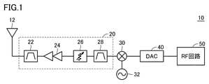
- FIG. 1 is a block diagram of a communication device 10 having a high frequency front-end circuit 20 to which the filter device of the first embodiment is applied.
- the communication device 10 is, for example, a mobile phone base station.
- the communication device 10 includes an antenna 12, a high frequency front end circuit 20, a mixer 30, a local oscillator 32, a digital-to-analog converter (DAC) 40, and an RF circuit 50. Further, the high frequency front end circuit 20 includes bandpass filters 22 and 28, an amplifier 24, and an attenuator 26. Note that FIG. 1 describes a case where the high-frequency front-end circuit 20 includes a transmission circuit that transmits a high-frequency signal from the antenna 12, but the high-frequency front-end circuit 20 is a reception circuit that receives a high-frequency signal via the antenna 12. May include.
- the communication device 10 up-converts the transmission signal transmitted from the RF circuit 50 into a high-frequency signal and radiates it from the antenna 12.
- the modulated digital signal which is a transmission signal output from the RF circuit 50, is converted into an analog signal by the D / A converter 40.
- the mixer 30 mixes the transmission signal converted from the digital signal to the analog signal by the D / A converter 40 with the oscillation signal from the local oscillator 32 and up-converts it into a high frequency signal.
- the bandpass filter 28 removes unnecessary waves generated by up-conversion and extracts only transmission signals in a desired frequency band.
- the attenuator 26 adjusts the strength of the transmitted signal.
- the amplifier 24 power-amplifies the transmitted signal that has passed through the attenuator 26 to a predetermined level.
- the bandpass filter 22 removes unnecessary waves generated in the amplification process and allows only signal components in the frequency band defined by the communication standard to pass through.
- the transmitted signal that has passed through the bandpass filter 22 is radiated
- a filter device corresponding to the present disclosure can be adopted.
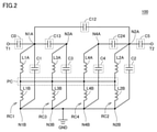
- FIG. 2 is an equivalent circuit diagram of the filter device 100.
- the filter device 100 includes an input terminal T1, an output terminal T2, and resonators RC1 to RC4.
- Each of the resonators RC1 to RC4 is an LC parallel resonator in which an inductor and a capacitor are connected in parallel.
- the resonator RC1 includes inductors L1A and L1B connected in series and capacitors C1 connected in parallel to the inductors L1A and L1B.
- the connection node N1A between the inductor L1A and the capacitor C1 is connected to the input terminal T1 via the capacitor C0.
- the connection node N1B between the inductor L1B and the capacitor C1 is connected to the ground terminal GND.
- the resonator RC2 includes inductors L2A and L2B connected in series and capacitors C2 connected in parallel to the inductors L2A and L2B.
- the connection node N2A between the inductor L2A and the capacitor C2 is connected to the output terminal T2 via the capacitor C5.
- the connection node N2B between the inductor L2B and the capacitor C2 is connected to the ground terminal GND.
- the resonator RC3 includes inductors L3A and L3B connected in series and capacitors C3 connected in parallel to the inductors L3A and L3B.
- the connection node N3A between the inductor L3A and the capacitor C3 is connected to the connection node N1A of the resonator RC1 via the capacitor C13.
- the connection node N3B between the inductor L3B and the capacitor C3 is connected to the ground terminal GND.
- the resonator RC4 includes inductors L4A and L4B connected in series and capacitors C4 connected in parallel to the inductors L4A and L4B.
- the connection node N4A between the inductor L4A and the capacitor C4 is connected to the connection node N2A of the resonator RC2 via the capacitor C24.
- the connection node N4B between the inductor L4B and the capacitor C4 is connected to the ground terminal GND.
- connection node N1A of the resonator RC1 and the connection node N2A of the resonator RC2 are connected via the capacitor C12. Further, the connection nodes of the two inductors in each resonator are connected to each other. The portion to which the resonator is commonly connected corresponds to the common electrode PC described later in FIG. 4 and the like.
- Each resonator is coupled by magnetic coupling.
- the filter device 100 has a configuration in which a four-stage resonator magnetically coupled to each other is arranged between the input terminal T1 and the output terminal T2. By adjusting the resonance frequency of each resonator, the filter device 100 functions as a bandpass filter for passing a signal in a desired frequency band.
- the capacitor C0 connected to the input terminal T1 and the capacitor C5 connected to the output terminal T2 are not indispensable, and the resonators RC1 and RC2 may be directly connected to the input terminal T1 and the output terminal T2, respectively.
- FIG. 3 is an external perspective view of the filter device 100
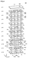
- FIG. 4 is an exploded perspective view showing an example of the laminated structure of the filter device 100.
- the filter device 100 includes a rectangular parallelepiped or substantially rectangular parallelepiped main body 110 formed by laminating a plurality of dielectric layers LY1 to LY12 in the stacking direction.
- the dielectric layers LY1 to LY12 are formed of, for example, a ceramic such as low temperature co-fired ceramics (LTCC: Low Temperature Co-fired Ceramics) or a resin.
- LTCC Low Temperature Co-fired Ceramics
- a plurality of electrodes provided in each dielectric layer and a plurality of vias provided between the dielectric layers form an inductor and a capacitor for forming an LC resonance circuit.
- "via” means a conductor provided in a dielectric layer for connecting electrodes provided in different dielectric layers. Vias are formed, for example, by conductive paste, plating, and / or metal pins.
- the stacking direction of the dielectric layers LY1 to LY12 in the main body 110 is defined as the “Z-axis direction”, and the direction perpendicular to the Z-axis direction and along the long side of the main body 110 is the “X-axis direction”.
- the direction along the short side of the main body 110 is defined as the "Y-axis direction”.
- the positive direction of the Z axis in each figure may be referred to as an upper side
- the negative direction may be referred to as a lower side.
- a directional mark DM for specifying the direction of the filter device 100 is arranged on the upper surface 111 (first layer LY1) of the main body 110.
- External terminals (input terminal T1, output terminal T2, and ground terminal GND) for connecting the filter device 100 and an external device are arranged on the lower surface 112 (12th layer LY12) of the main body 110.
- Each of the input terminal T1, the output terminal T2, and the ground terminal GND is a flat plate-shaped electrode, and is an LGA (Land Grid Array) terminal regularly arranged on the lower surface 112 of the main body 110.
- the filter device 100 has a four-stage LC parallel resonator. More specifically, a resonator RC1 including vias V1A, V1B and a capacitor electrode P2, a resonator RC2 including vias V2A, V2B and a capacitor electrode P8, vias V3A, V3B and a capacitor. It includes a resonator RC3 configured to include an electrode P3 and a resonator RC4 configured to include vias V4A, V4B and a capacitor electrode P7.
- the capacitor electrode P2 of the resonator RC1 and the capacitor electrode P8 of the resonator RC2 are provided in the 10th layer LY10.
- the capacitor electrode P2 faces the flat plate electrode P1 provided on the LY11 in the 11th layer.
- the capacitor C0 of FIG. 2 is configured by the capacitor electrode P2 and the flat plate electrode P1.
- the flat plate electrode P1 is connected to the input terminal T1 provided in the twelfth layer LY12 by the via V0.
- the capacitor electrode P8 faces the flat plate electrode P9 provided on the LY11 in the 11th layer.
- the capacitor C5 of FIG. 2 is configured by the capacitor electrode P8 and the flat plate electrode P9.
- the flat plate electrode P9 is connected to the output terminal T2 provided in the twelfth layer LY12 by the via V5.
- the capacitor electrode P2 of the resonator RC1 is connected to the common electrode PC provided in the second layer LY2 by the via V1A. Further, the common electrode PC is connected to the flat plate electrode PG1 provided in the 9th layer LY9 by the via V1B.
- the flat plate electrode PG1 is connected to the flat plate electrode PG2 provided in the 11th layer LY11 by the vias VG1, VG2, and VG3. Further, the flat plate electrode PG2 is connected to the ground terminal GND provided in the 12th layer LY12 by the vias VG4 and VG5.
- a part of the capacitor electrode P2 also faces the flat plate electrode PG1, and the capacitor electrode P2 and the flat plate electrode PG1 form the capacitor C1 in FIG. 2.
- the via V1A and the via V1B correspond to the inductor L1A and the inductor L1B in FIG. 2, respectively.
- the capacitor electrode P8 of the resonator RC2 is connected to the common electrode PC provided in the second layer LY2 by the via V2A. Further, the common electrode PC is connected to the flat plate electrode PG1 provided in the 9th layer LY9 by the via V2B. A part of the capacitor electrode P8 also faces the flat plate electrode PG1, and the capacitor electrode P8 and the flat plate electrode PG1 form the capacitor C2 in FIG. 2.
- the via V2A and the via V2B correspond to the inductor L2A and the inductor L2B in FIG. 2, respectively.
- the capacitor electrode P3 of the resonator RC3 and the capacitor electrode P7 of the resonator RC4 are provided on the eighth layer LY8.
- the capacitor electrode P3 is connected to the common electrode PC provided in the second layer LY2 by the via V3A. Further, the common electrode PC is connected to the flat plate electrode PG1 provided in the 9th layer LY9 by the via V3B.
- the capacitor electrode P3 faces the flat plate electrode PG1, and the capacitor electrode P3 and the flat plate electrode PG1 form the capacitor C3 of FIG. 2.
- the via V3A and the via V3B correspond to the inductor L3A and the inductor L3B in FIG. 2, respectively.
- the capacitor electrode P7 is connected to the common electrode PC provided in the second layer LY2 by the via V4A. Further, the common electrode PC is connected to the flat plate electrode PG1 provided in the 9th layer LY9 by the via V4B. The capacitor electrode P7 faces the flat plate electrode PG1, and the capacitor electrode P7 and the flat plate electrode PG1 form the capacitor C4 of FIG. 2.
- the via V4A and the via V4B correspond to the inductor L4A and the inductor L4B in FIG. 2, respectively.
- the via V1A of the resonator RC1 is also connected to the flat plate electrode P4 provided in the seventh layer LY7.
- a part of the flat plate electrode P4 faces the capacitor electrode P3 of the resonator RC3.
- the plate electrode P4 and the capacitor electrode P3 constitute the capacitor C13 in FIG. 2.
- the via V2A of the resonator RC2 is also connected to the flat plate electrode P6 provided in the seventh layer LY7.
- a part of the flat plate electrode P6 faces the capacitor electrode P7 of the resonator RC4.
- the plate electrode P6 and the capacitor electrode P7 constitute the capacitor C24 in FIG. 2.
- the flat plate electrodes P4 to P6 constitute the capacitor C12 in FIG. 2.
- first via the vias V1A, V2A, V3A, and V4A connected to the ground terminal GND via the capacitor in each resonator
- second vias the vias V1B, V2B, V3B, and V4B connected to the ground terminal GND without passing through a capacitor in each resonator are referred to as "second vias”.
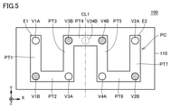
- FIG. 5 is a plan view of the common electrode PC in the filter device 100.
- the common electrode PC is composed of a band-shaped wiring pattern having a first end portion E1 and a second end portion E2.
- the common electrode PC has wiring patterns PT1, PT3, PT5, PT7 along the short side (Y-axis) of the main body 110 and wiring patterns PT2, PT4, along the long side (X-axis) of the main body 110. It has a meander shape in which PT6 and PT6 are alternately connected.
- the line widths of the wiring patterns PT1 to PT7 are the same.
- Via V1A of the resonator RC1 is connected to the first end E1 of the common electrode PC (that is, one end of the wiring pattern PT1).
- the via V1B of the resonator RC1 is connected to the other end of the wiring pattern PT1 (that is, one end of the wiring pattern PT2).
- the via V3A of the resonator RC3 is connected to the other end of the wiring pattern PT2 (that is, one end of the wiring pattern PT3).
- the via V3B of the resonator RC3 is connected to the other end of the wiring pattern PT3 (that is, one end of the wiring pattern PT4).
- the via V4B of the resonator RC4 is connected to the other end of the wiring pattern PT4 (that is, one end of the wiring pattern PT5).
- the via V4A of the resonator RC3 is connected to the other end of the wiring pattern PT5 (that is, one end of the wiring pattern PT6).
- the via V2B of the resonator RC2 is connected to the other end of the wiring pattern PT6 (that is, one end of the wiring pattern PT7).
- the via V2A of the resonator RC2 is connected to the other end of the wiring pattern PT7 (that is, the second end portion E2 of the common electrode PC).
- each via is arranged so as to be axisymmetric with respect to the virtual line CL1 in order to ensure the symmetry of the filter characteristics.
- the via V1B (second via) of the resonator RC1 is arranged between the via V1A of the resonator RC1 and the via V3A (first via) of the resonator RC3 along the common electrode PC. .. Further, a via V2B (second via) of the resonator RC2 is arranged between the via V2A of the resonator RC2 and the via V4A (first via) of the resonator RC4 along the common electrode PC.
- the via V3A of the resonator RC3 and the via V4A (first via) of the resonator RC4 the via V3B of the resonator RC3 and the via V3B of the resonator RC4 (second via). Is arranged.
- the second via is connected between the portions of the two adjacent resonators to which the first via is connected in the path along the common electrode PC. Since the adjacent vias V3B and via V4B are both connected to the ground terminal GND via the flat plate electrodes PG1 and PG2 and vias VG1, VG2, VG3, VG4 and VG5, these two vias are shown in FIG. It can be thought of as one via, such as the broken via V34B in. Then, the first via and the second via are alternately arranged from the first end portion E1 to the second end portion E2 along the common electrode PC.
- a plurality of LC parallel resonators are connected to the band-shaped common electrode and connected to the ground terminal GND via the capacitor, and to the ground terminal GND without the capacitor.
- adjacent resonators are inductively coupled to each other.
- a configuration is known in which the line conductors constituting each resonator are arranged apart from each other.
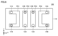
- Patent Document 1 International Publication No. 2019/097774 (Patent Document 1), as in the filter device 200 shown in FIG. 6, the vias constituting the inductor of each resonator are individually independent of each other for each resonator. It is connected by wiring electrodes PD1 to PD4.
- the Q value is affected by the air core diameter of the inductor in each resonator, that is, the via spacing. Specifically, the larger the air core diameter of the inductor in each resonator, the higher the Q value tends to be. Therefore, in the filter device, the vias are arranged so that the via spacing of each resonator is as wide as possible.
- the strength of the magnetic coupling between the resonators can be adjusted by the distance (interval) between the resonators, but in the case of a multi-stage filter device, the resonators are coupled to each other, and a specific resonator is used. Adjustment by the distance between the resonators may be difficult in design because the coupling state of other resonators may change when the distance between the resonators is changed. Therefore, the Q value may be low due to the simplicity of design, but a method of adjusting the coupling state by changing the via spacing is generally used. However, when the filter device is further miniaturized, the degree of freedom in arranging the vias is further limited, and there is a possibility that the desired filter characteristics cannot be realized.
- vias constituting the inductors of the plurality of LC parallel resonators RC1 to RC4 are connected to the common electrode PC and connected to the ground terminal GND via the capacitor.
- the "first via” to be connected and the “second via” connected to the ground terminal GND without a capacitor are arranged alternately along the common electrode PC.
- the coupling state between the resonators can be changed by adjusting the shape of the common electrode (for example, the line width or the line length).
- the via can be arranged at a position where the optimum Q value can be realized, so that it is possible to adjust the magnetic coupling between the resonators while suppressing the decrease in the Q value.
- FIG. 7 shows the insertion loss (solid line LN10) from the input terminal T1 to the output terminal T2 in the filter device 100 having the common electrode PC having the shape shown in FIG. 5, and the filter device 200 of the comparative example shown in FIG. It is a figure which showed the insertion loss (dashed line LN11).
- FIG. 7 (b) in the lower row is an enlarged view of a portion of the region RG1 in FIG. 7 (a) in the upper row.
- the attenuation pole in the non-passing band on the low frequency side of the pass band moves to the pass band side as compared with the filter device 200 of the comparative example.
- the filter device 100 of the first embodiment the amount of attenuation of the attenuation pole in the non-passing band on the higher frequency side than the pass band is larger than that of the filter device 200 of the comparative example.
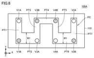
- FIG. 8 is a plan view of the common electrode PC in the filter device 100A.
- the line width W1 of the wiring pattern PT2 and the wiring pattern PT6 in the common electrode PC is wider than that of the common electrode PC of the filter device 100 shown in FIG. That is, in the filter device 100A, the line width of the wiring pattern PT2 and the wiring pattern PT6 in the common electrode PC is wider than the line width of the wiring patterns PT1, PT3, PT4, PT5, PT7.
- FIG. 8 is a plan view of the common electrode PC in the filter device 100A.
- FIG. 9 is a diagram showing an insertion loss in the filter device 100A having the common electrode PC having the shape shown in FIG.
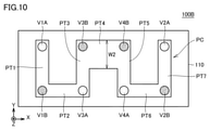
- FIG. 10 is a plan view of the common electrode PC in the filter device 100.
- the line width W2 of the wiring pattern PT4 in the common electrode PC is wider than that in the common electrode PC of the filter device 100 shown in FIG. That is, in the filter device 100B, the line width of the wiring pattern PT4 in the common electrode PC is wider than the line width of the wiring patterns PT1 to PT3 and PT5 to PT7.
- FIG. 11 is a diagram showing an insertion loss in a filter device 100B having a common electrode PC having the shape shown in FIG. In FIGS. 9 and 11, for comparison, the insertion loss in the case of FIG. 5 is shown by the broken line LN10.
- each resonator is connected by a common electrode, and the shape of the common electrode is changed to obtain magnetic coupling between the resonators.
- the coupling state can be adjusted according to the desired filter characteristics. In this case, since it is not necessary to change the arrangement of the vias constituting the inductor in each resonator, it is possible to suppress a decrease in the Q value.
- FIG. 12 is a plan view of the common electrode PC1 in the filter device 100C of the modification 1.
- the filter device 100C is an example of a configuration including three LC parallel resonators.
- the first vias V10A, V11A, V12A in each resonator are arranged along one long side parallel to the X axis in the main body 110, and the other long side.
- the second vias V10B and V11B are arranged along the above.
- the common electrode PC1 is provided in a substantially W shape so as to reach the via V12A from the via V10A via the via V10B, the via V11A, and the via V11B. That is, in the common electrode PC1, the first vias and the second vias are alternately arranged in a zigzag shape along the path from the first end to the second end.
- the second via of the resonator including the via V11A is shared with the via V10B and / or the via V11B in order to arrange the vias line-symmetrically with respect to the virtual line CL1. ..
- the first and second stages are used.
- the magnetic coupling of the resonator and the magnetic coupling of the first and third stage resonators can be adjusted.
- the magnetic coupling of the second-stage and third-stage resonators is performed. Can be adjusted.
- the magnetic coupling of the second-stage and third-stage resonators is performed.
- the magnetic coupling of the first and third stage resonators can be adjusted.
- each resonator is connected to the common electrode and the line width of the common electrode is changed to resonate without changing the via position.
- the coupling state between the vessels can be adjusted. Therefore, it is possible to adjust the coupling between the resonators while suppressing the decrease in the Q value.
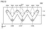
- FIG. 13 is a plan view of the common electrode PC2 in the filter device 100D of the modification 2.
- the filter device 100D includes four LC parallel resonators as in the first embodiment, but the arrangement of vias is different from that of the filter device 100.
- the first vias V20A to V23A are arranged along one long side of the main body 110, and the first vias V20A to V23A are arranged along the other long side, as in the first modification.
- Two vias V20B to V22B are arranged.
- the common electrode PC2 is provided from the via V20A to the via V23A via the via V20B, the via V21A, the via V21B, the via V22A, and the via V22B. That is, in the common electrode PC2, the first vias and the second vias are alternately arranged in a zigzag shape along the path from the first end to the second end.
- the second via of one of the resonators is shared with the second via of the adjacent resonator.
- the line width of the wiring pattern connecting the vias V20A and V20B and the wiring pattern connecting the vias V20B and V21A is adjusted in the direction of the arrow AR21 to perform the first and second stages.
- the magnetic coupling of the resonators, the magnetic coupling of the first-stage and third-stage resonators, and the magnetic coupling of the first-stage and fourth-stage resonators can be adjusted.
- the magnetic coupling of the second-stage and third-stage resonators is performed. Can be adjusted.
- the magnetic coupling of the first-stage and fourth-stage resonators is performed.
- the magnetic coupling of the second and fourth stage resonators and the magnetic coupling of the third and fourth stage resonators can be adjusted.
- each resonator is connected to the common electrode and the line width of the common electrode is changed so that the via position is not changed between the resonators.
- the coupling state can be adjusted. Therefore, it is possible to adjust the coupling between the resonators while suppressing the decrease in the Q value.
- FIG. 14 is a plan view of the common electrode PC3 in the filter device 100E of the modification 3.
- the filter device 100E is an example of a configuration including five LC parallel resonators.
- the first via V30A, the second via V31B, the second via V32B, and the first via V34A are arranged along one long side of the main body 110, and the other.
- the second via V30B, the first via V31A to V33A, and the second via V33B are arranged along the long side of the above.
- the common electrode PC3 is provided from the via V30A to the via V34A via the via V30B, the via V31A, the via V31B, the via V32A, the via V32B, the via V33A, and the via V33B.
- the second via of one of the resonators is shared with the second via of the adjacent resonator.
- the vias may be arranged in a zigzag shape as in the modified example 1 and the modified example 2.
- the first and second stages are used.
- Adjust the magnetic coupling of the resonator, the magnetic coupling of the 1st and 3rd stage resonators, the magnetic coupling of the 1st and 4th stage resonators, and the magnetic coupling of the 1st and 5th stage resonators. can do.
- the magnetic coupling of the second-stage and third-stage resonators is performed.
- the magnetic coupling of the second and fourth stage resonators can be adjusted.
- the magnetic coupling of the second-stage and fourth-stage resonators is performed.
- the magnetic coupling of the third and fourth stage resonators can be adjusted.
- the magnetic coupling of the first-stage and fifth-stage resonators is performed.
- the magnetic coupling of the second and fifth stage resonators, the magnetic coupling of the third and fifth stage resonators, and the magnetic coupling of the fourth and fifth stage resonators can be adjusted.
- each resonator is connected to the common electrode and the line width of the common electrode is changed to resonate without changing the via position.
- the coupling state between the vessels can be adjusted. Therefore, it is possible to adjust the coupling between the resonators while suppressing the decrease in the Q value.
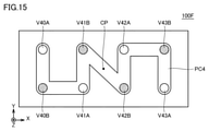
- FIG. 15 is a plan view of the common electrode PC4 in the filter device 100F of the modified example 4.
- the filter device 100F includes four LC parallel resonators as in the first embodiment and the second modification, but the arrangement of vias is further different. More specifically, in the filter device 100F, the vias are arranged so as to be point-symmetrical.
- the first via V40A, the second via V41B, the first via V42A, and the second via V43B are arranged along one long side of the main body 110, and the other.
- the second via V40B, the first via V41A, the second via V42B, and the first via V43A are arranged along the long side of the above.
- the common electrode PC4 is provided so as to reach the via V43A from the via V40A via the via V40B, the via V41A, the via V41B, the via V42B, the via V42A, and the via V43B.
- vias are arranged so as to be point-symmetrical with respect to the point CP.
- the resonators are connected to the common electrode and the line width of the common electrode is changed without changing the via position.
- the coupling state between them can be adjusted. Therefore, it is possible to adjust the coupling between the resonators while suppressing the decrease in the Q value.
- FIGS. 8 and 10 of the first embodiment a method of adjusting the magnetic coupling by adjusting the line width of the wiring pattern connecting the resonators has been described.
- FIG. 16 is an exploded perspective view showing an example of the laminated structure of the filter device 100G of the second embodiment. Further, FIG. 17 is a plan view of the common electrode PC1 in the filter device 100G of FIG.
- the common electrode PC in the filter device 100 described in FIG. 4 of the first embodiment is replaced with the common electrode PC1, and the vias V3B and V4B are as described in FIG. It has been replaced with one via V34B, and a flat plate electrode P10 provided in the seventh layer LY7 has been added.
- the description of the elements overlapping with FIG. 4 is not repeated.
- the flat plate electrode P10 has a substantially U-shape, and is arranged between the flat plate electrode P4 and the flat plate electrode P6 in the seventh layer LY7.
- the flat plate electrode P10 is connected to the via V34B, and is connected to the common electrode PC1 and the flat plate electrode PG1 (that is, the ground terminal GND) via the via V34B.
- the flat plate electrode P10 is capacitively coupled to the flat plate electrode P5 provided in the sixth layer LY6 and the capacitor electrodes P3 and P7 provided in the eighth layer LY8.
- the plate electrode P10 increases the capacitance of the capacitors C1 to C4 (FIG. 2) in the resonators RC1 to RC4.
- the connection position of is moved in the positive direction of the Y axis.
- the wiring pattern PT2 is formed between the portion of the wiring pattern PT1 to which the via V1A (first via) of the resonator RC1 is connected and the portion to which the via V1B (second via) is connected, and wiring.
- the wiring pattern PT6 includes a portion of the wiring pattern PT7 to which the via V2A (first via) of the resonator RC2 is connected and a portion to which the via V2B (second via) is connected, and a wiring pattern. It is connected between the portion of the resonator RC4 in PT5 to which the via V4A (first via) is connected and the portion to which the via V34B (second via) is connected.
- the wiring pattern PT2 connecting the resonator RC1 and the resonator RC3 approaches the open end side (that is, the via V1A side) of the resonator RC1, the shortest distance of the path from the via V1A to the via V34B becomes shorter.
- the magnetic coupling between the resonator RC1 and the resonator RC3 can be strengthened.
- the wiring pattern PT6 connecting the resonator RC2 and the resonator RC4 approaches the open end side (that is, the via V2A side) of the resonator RC4, so that the shortest distance of the path from the via V2A to the via V34B is reduced.
- the magnetic coupling between the resonator RC2 and the resonator RC4 can be strengthened. That is, the resonator RC1 is adjusted by adjusting the distance LG1 from the end of the wiring pattern PT1 on the via V1A side to the wiring pattern PT2 and the distance LG1 from the end of the wiring pattern PT7 on the via V2A side to the wiring pattern PT6. , The magnetic coupling between RC2 and other resonators can be adjusted.
- the inductance value of the wiring patterns PT2 and PT6 can be adjusted by adjusting the line width W1 of the wiring patterns PT2 and PT6. Further, as described with reference to FIG. 10, the inductance value of the wiring pattern PT4 can be adjusted by adjusting the line width W2 of the wiring pattern PT4 between the resonators RC3 and RC4.
- the wiring patterns PT2 and PT6 have the negative side of the Y-axis fixed to the end of the wiring patterns PT1 and PT7 on the negative side of the Y-axis.
- the line width W1 if the line width W1 is narrowed and the inductance value is increased, the distance LG1 becomes long, so that the magnetic coupling between the resonators becomes weak.
- the line width W1 is widened and the inductance value is made small, the distance LG1 becomes short, so that the magnetic coupling between the resonators becomes strong. That is, the magnitude of the inductance value of the inductor connecting the resonators and the magnetic coupling between the resonators change in conjunction with each other. Therefore, for example, when it is desired to increase the inductance value between the resonators and further strengthen the magnetic coupling between the resonators, such as in a small filter device, the desired filter characteristics cannot be realized by such an adjustment method. Cases can occur.
- the inductance value between the resonators is adjusted by the line width W1 of the wiring patterns PT2 and PT6, and the magnetic coupling between the resonators is the connection position of the wiring patterns PT2 and PT6 (that is, that is).
- the distance LG1 By adjusting the distance LG1, the inductance value between the resonators and the magnetic coupling between the resonators can be adjusted independently. Therefore, the degree of freedom in design is increased, and it becomes easy to realize desired filter characteristics.
- Increasing the inductance value between the resonators has the effect of increasing the impedance of the resonator.
- Increasing the magnetic coupling between the resonator RC1 and the resonator RC4 has the effect of shifting the attenuation pole near the passband to the passband side. Further, by increasing the magnetic coupling between the resonator RC2 and the resonator RC3, the pass bandwidth can be expanded.
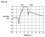
- FIG. 18 shows the connection positions of the wiring patterns PT2 and PT6 in the filter device 100G of the second embodiment and the filter device 100 of the first embodiment with the wiring patterns PT2 and PT6 having the same line width W1. That is, it is a figure comparing the insertion loss when the distance LG1) is changed.
- the connection positions of the wiring patterns PT2 and PT6 in the filter device 100G are closer to the vias V1A and V2A than the connection positions of the wiring patterns PT2 and PT6 in the filter device 100.
- the solid line LN40 shows the case of the filter device 100G
- the broken line LN41 shows the case of the filter device 100.
- the frequency at which the attenuation pole is generated is closer to the pass band side than the filter device 100 due to the stronger magnetic coupling between the resonators. That is, the steepness of attenuation in the non-passband can be increased.
- the line width W2 and the connection position may be individually adjusted for the wiring pattern PT4 that connects the resonator RC3 and the resonator RC4.
- the degree of freedom in design is achieved by individually adjusting the inductance value by the line width of the wiring pattern connecting each resonator and adjusting the magnetic coupling between the resonators by the connection position of the wiring pattern. Can be enhanced to achieve the desired filter characteristics.
- the "wiring pattern PT2" and “wiring pattern PT6" in the second embodiment correspond to the "first part” and the “second part” in the present disclosure, respectively.
- FIG. 19 is an equivalent circuit diagram of the filter device 100H according to the third embodiment.
- the capacitors C0 and C5 provided at the input / output ends in the equivalent circuit of the filter device 100 shown in FIG. 2 are removed, and the inductors L3B and L4B in the resonators RC3 and RC4 are shared as the inductor L34B. Further, the resonators RC3 and RC4 are coupled by the capacitor C34.
- FIG. 19 the description of the elements overlapping with FIG. 2 will not be repeated.
- FIG. 20 is an exploded perspective view showing an example of the laminated structure of the filter device 100H of the third embodiment.
- the resonators RC1 to RC4 are configured in the main body 110 having the plurality of dielectric layers LY1 to LY12, similarly to the filter device 100.
- the resonator RC1 includes vias V51A and V51B and a capacitor electrode P12.
- the resonator RC2 includes vias V52A, V52B and a capacitor electrode P19.
- the resonator RC3 includes vias V53A, V534B and a capacitor electrode P13.
- the resonator RC4 includes vias V54A, V534B and a capacitor electrode P18.
- a directional mark DM for specifying the direction of the filter device 100 is arranged on the upper surface 111 (first layer LY1) of the main body 110. Further, an external terminal (input terminal T1, output terminal T2, and ground terminal GND) for connecting to an external device is arranged on the lower surface 112 (12th layer LY12) of the main body 110.
- the input terminal T1 is connected to the flat plate electrode P11 of the 11th layer LY11 by the via V50.
- the via V51A of the resonator RC1 is connected to the flat plate electrode P11.
- the via V51A is connected to the common electrode PC11 provided in the second layer LY2.
- the common electrode PC11 is connected to the flat plate electrode PG11 provided in the 10th layer LY10 by the via V51B.
- the flat plate electrode PG11 is connected to the ground terminal GND provided in the 12th layer LY12 by the vias VG4 and VG5.
- the via V51A is connected to the capacitor electrode P12 in the 9th layer LY9, and further connected to the capacitor electrode P14 in the 7th layer LY7. A part of the capacitor electrode P12 faces the flat plate electrode PG11 of the 10th layer LY10. The capacitor electrode P12 and the flat plate electrode PG11 constitute the capacitor C1 in FIG. 19.
- the via V51A and the via V51B correspond to the inductor L1A and the inductor L1B in FIG. 19, respectively.
- the output terminal T2 is connected to the flat plate electrode P20 of the 11th layer LY11 by the via V55.
- the via V52A of the resonator RC2 is connected to the flat plate electrode P20.
- the via V52A is connected to the common electrode PC11 of the second layer LY2. Further, the common electrode PC11 is connected to the flat plate electrode PG11 provided in the 10th layer LY10 by the via V52B.
- the via V52A is connected to the capacitor electrode P19 in the 9th layer LY9, and further connected to the capacitor electrode P17 in the 7th layer LY7. A part of the capacitor electrode P19 faces the flat plate electrode PG11 of the 10th layer LY10. The capacitor electrode P19 and the flat plate electrode PG11 constitute the capacitor C2 in FIG. 19.
- the via V52A and the via V52B correspond to the inductor L2A and the inductor L2B in FIG. 19, respectively.
- the capacitor electrode P14 provided in the 7th layer LY7 faces the capacitor electrode P13 of the resonator RC3 provided in the 8th layer LY8.
- the capacitor electrode P13 and the capacitor electrode P14 constitute the capacitor C13 in FIG. 19.
- the capacitor electrode P13 is connected to the common electrode PC11 of the second layer LY2 by the via V53A. Further, the common electrode PC11 is connected to the flat plate electrode PG11 of the 10th layer LY10 by the via V534B. The capacitor electrode P13 faces the flat plate electrode PG11, and the capacitor electrode P13 and the flat plate electrode PG11 constitute the capacitor C3 of FIG.
- the via V53A corresponds to the inductor L3A in FIG. Further, the via V534B corresponds to the inductor L34B in FIG.
- the capacitor electrode P17 of the 7th layer LY7 faces the capacitor electrode P18 of the resonator RC4 provided in the 8th layer LY8.
- the capacitor electrode P17 and the capacitor electrode P18 constitute the capacitor C24 in FIG. 19.
- the capacitor electrode P18 is connected to the common electrode PC11 of the second layer LY2 by the via V54A. Further, the common electrode PC11 is connected to the flat plate electrode PG11 of the 10th layer LY10 by the via V534B as described above. The capacitor electrode P18 faces the flat plate electrode PG11, and the capacitor electrode P18 and the flat plate electrode PG11 constitute the capacitor C4 of FIG.
- the via V54A corresponds to the inductor L4A in FIG.
- the capacitor electrodes P14, P15, and P17 constitute the capacitor C12 in FIG. 19.
- the sixth layer LY6 is further provided with a capacitor electrode P16.
- the capacitor electrode P16 partially faces the capacitor electrodes P13 and P18 of the eighth layer LY8.
- the capacitor electrodes P13, P16, and P18 constitute the capacitor C34 in FIG. 19.
- the vias V51A, V52A, V53A, and V54A connected to the ground terminal GND via the capacitor in each resonator are referred to as "first vias”.
- the vias V51B, V52B, and V534B connected to the ground terminal GND without passing through a capacitor in each resonator are referred to as "second vias”.
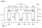
- FIG. 21 is a plan view of the common electrode PC 11 in the filter device 100H.
- the common electrode PC 11 is configured by a band-shaped wiring pattern having a first end portion E11 and a second end portion E12. As shown in FIG. 21, the common electrode PC 11 extends along the wiring patterns PT11, PT14, PT16 extending along the short side (Y axis) of the main body 110 and along the long side (X axis) of the main body 110. Wiring patterns PT12, PT13, and PT15 are included. The wiring patterns PT12, PT13, and PT15 are connected in series between the wiring pattern PT11 and the wiring pattern PT16. The wiring pattern PT14 is connected to the wiring pattern PT13. That is, the common electrode PC 11 has a substantially E-shape.
- the via V51A of the resonator RC1 is connected to the first end portion E11 of the common electrode PC11 (that is, one end of the wiring pattern PT11).
- the via V51B of the resonator RC1 is connected to the other end of the wiring pattern PT11.
- the via V52A of the resonator RC2 is connected to the second end E12 (that is, one end of the wiring pattern PT16) of the common electrode PC11.
- the via V52B of the resonator RC2 is connected to the other end of the wiring pattern PT12.
- the via V53A of the resonator RC3 is connected to the end portion on the wiring pattern PT11 side. Further, in the wiring pattern PT13, the via V54A of the resonator RC4 is connected to the end portion on the wiring pattern PT16 side.
- the wiring pattern PT12 is connected between the wiring pattern PT11 and the wiring pattern PT13.
- the wiring pattern PT15 is connected between the wiring pattern PT11 and the wiring pattern PT16.
- Via V534B which is common to the resonators RC3 and RC4, is connected to one end of the wiring pattern PT14.
- the other end of the wiring pattern PT14 is connected to the wiring pattern PT13.
- the via V51A, the via V51B, the via V53A, the via V54A, the via V52B, and the via V52A are formed along the common electrode PC11 from the first end portion E11 to the second end portion E12. They are connected to the common electrode PC11 in order.
- FIG. 5 shows that the common electrode PC11 has a substantially E-shape, and the portion to which the via V53A of the resonator RC3 is connected and the portion to which the via 54A of the resonator RC4 is connected are adjacent to each other.
- the shortest distance along the common electrode PC11 between the via V51A of the resonator RC1 and the via V54A of the resonator RC4 is shorter than that of the meander-shaped common electrode PC of the first embodiment shown. That is, the magnetic coupling between the resonator RC1 and the resonator RC4 is stronger than that of the filter device 100 of the first embodiment.
- the shortest distance along the PC 11 is also shortened.
- the magnetic coupling between the resonator RC2 and the resonator RC3 and the magnetic coupling between the resonator RC1 and the resonator RC2 become stronger.
- the magnetic coupling between the first-stage resonator and the third-stage resonator, and the second-stage resonator and the fourth stage resonator are present. It is known that when the magnetic coupling with the resonator of the stage is strengthened, the amount of attenuation on the high frequency side of the passing band increases. Further, it is known that when the magnetic coupling between the first-stage resonator and the fourth-stage resonator is strengthened, the attenuation on the low frequency side of the pass band increases. Therefore, by shaping the common electrode PC 11 as shown in FIG. 21, it is possible to improve the attenuation characteristics in the vicinity of the pass band.
- FIG. 22 is a diagram for explaining the passing characteristics of the filter device 100H of FIG.
- the horizontal axis shows the frequency
- the vertical axis shows the insertion loss.
- a portion on the high frequency side of the pass band is shown.
- the solid line LN50 in FIG. 22 shows the case of the filter device 100H of the third embodiment
- the broken line LN51 shows the case of the filter device 100 of the first embodiment.
- the filter device 100H (solid line LN50) has a larger insertion loss (attenuation amount) on the high frequency side than the attenuation pole as compared with the filter device 100 (dashed line LN51). Therefore, in the filter device 100H, the damping characteristics can be further improved as compared with the configuration of the first embodiment.
- the distance LG11 of the wiring patterns PT12 and PT15 from the positive end of the common electrode PC11 in the positive direction is changed to adjust the line width of the wiring patterns PT12 and PT15. Then, since the shortest distance between the vias does not change, the inductance value between the resonators can be changed while maintaining the degree of magnetic coupling.
- the distance LG12 of the wiring patterns PT12 and PT15 from the negative end of the common electrode PC11 in the negative direction is changed to adjust the line width of the wiring patterns PT12 and PT15. Since the shortest distance between the vias changes, the strength of the magnetic coupling can be changed and the inductance value between the resonators can be adjusted.
- the distance LG13 between the via V53A and the via V54A is shortened, the distance between the resonator RC1 and the resonator RC4, the distance between the resonator RC2 and the resonator RC3, and the distance between the resonator RC3 and the resonator RC4. Can be shortened, so that the magnetic coupling between these resonators can be strengthened.
- the distance between the resonator RC1 and the resonator RC3 and the distance between the resonator RC2 and the resonator RC4 become long, the magnetic coupling between these resonators weakens and the impedance at the input / output end changes. This change in impedance can be matched, for example, by adjusting the values of the capacitors (capacitors C13 and C24 in FIG. 19) between the resonators.
- FIG. 23 is a plan view of the common electrode PC11A in the filter device 100H1 of the modified example 5.
- the resonators RC3 and RC4 have a configuration in which vias connecting the common electrode PC11A and the flat plate electrode PG11 are individually arranged.
- the wiring patterns PT13 and PT14 in FIG. 21 are configured as one wiring pattern P134, and the inductors in the resonators RC3 and RC4 are not shared as one inductor, and vias.
- the via V53B is arranged for the V53A, and the via V53B is arranged for the via V54A.
- the magnetic coupling between the resonator RC3 and the resonator RC4 is weaker than that of the filter device 100H, so that the amount of attenuation of the attenuation pole near the pass band increases while the pass band.
- the width becomes slightly narrower.
- FIG. 24 is a plan view of the common electrode PC11B in the filter device 100H2 of the modification 6.
- the common electrode PC11B has a wiring pattern PT11, PT16, PT17, PT18 extending along the short side (Y axis) of the main body 110 and a wiring pattern PT12 extending along the long side (X axis) of the main body 110. Includes PT13 and PT15.
- the wiring pattern PT12 is connected between the wiring pattern PT11 and the wiring pattern PT17.
- the wiring pattern PT13 is connected between the wiring pattern PT17 and the wiring pattern PT18.
- the wiring pattern PT15 is connected between the wiring pattern PT18 and the wiring pattern PT16.
- the position of the via V53A and the position of the via V53B in the resonator RC3 are exchanged with each other as compared with the filter device 100H1 of the modification 5 shown in FIG. 23, and the position of the via V54A and the via in the resonator RC4 are exchanged.
- the configuration is such that the position of V54B is exchanged.
- the via V51B in the resonator RC1 is shared with the via V53B in the resonator RC3 and deleted
- the via V52B in the resonator RC2 is shared with the via V54B in the resonator RC4 and deleted. There is.
- vias V51A, V52A, V53A, and V54A connected to the ground terminal GND via a capacitor are connected to the negative end of the Y-axis of the wiring patterns PT11, PT16, PT17, and PT18, respectively, and the wiring pattern.
- Vias V53B and V54B connected to the ground terminal GND without a capacitor are connected to the positive end of the Y-axis of PT17 and PT18, respectively.
- the resonator RC1 and the resonator RC1 are more than the configuration of the filter device 100H1 of the modified example 5.
- the magnetic coupling between the resonator RC3 and the resonator RC2 and the resonator RC4 become stronger. Therefore, the amount of attenuation on the high frequency side of the pass band can be increased.
- a configuration in which the vias are arranged in the same arrangement as in the filter device 100H2 is adopted, or as in the filter device 100H1. Whether or not to adopt a configuration in which the vias are arranged in the opposite directions to each other is appropriately selected based on, for example, the size of the entire filter device.
- the size of the filter device particularly the dimension in the Z-axis direction
- the length of the via becomes long and the air core diameter of the coil in each resonator becomes large. Therefore, if the vias of the resonator are arranged in the same manner as in the filter device 100H2 of the modified example 6, the magnetic coupling may become excessive. In such a case, it is preferable to adopt a configuration in which the vias are arranged in the opposite directions to each other as in the filter device 100H1 of the modified example 5 to weaken the magnetic coupling to realize the desired filter characteristics.
- the size of the filter device especially the dimension in the Z-axis direction
- the length of the via is short, so that the magnetic coupling between the resonators tends to be weak. Therefore, it is preferable to realize the desired filter characteristics by strengthening the magnetic coupling by arranging the vias of the resonator in the same arrangement as in the filter device 100H2 of the modification 6.
- the degree of coupling between the resonators can be adjusted by adjusting the line widths of the wiring patterns PT12, PT13, and PT15.
- the common electrode is arranged in the second layer LY2 on the uppermost side of the main body 110. Since this common electrode is a passage path for the current flowing in the resonator, if an external shield is present on the upper surface side of the filter device, capacitive coupling with the external shield will occur, which causes fluctuations in the filter characteristics. Can be.
- the communication device main body should be downsized to secure the distance. It can be a hindrance factor.
- an internal shield connected to the ground terminal GND is arranged in a layer on the upper surface side of the common electrode. This makes it possible to suppress fluctuations in the filter characteristics due to the external shield.
- FIG. 25 is an exploded perspective view showing an example of the laminated structure of the filter device 100I of the fourth embodiment.
- the resonators RC1 to RC4 are configured in the main body 110 having the plurality of dielectric layers LY1 to LY12, similarly to the filter device 100.
- the filter device 100I has a configuration in which the capacitor C34 in the equivalent circuit of the filter device 100H of the third embodiment shown in FIG. 19 is removed.
- the resonator RC1 includes vias V61A, V61B and a capacitor electrode P21.
- the resonator RC2 includes vias V62A, V62B and a capacitor electrode P28.
- the resonator RC3 includes vias V63A, V634B and a capacitor electrode P22.
- the resonator RC4 includes vias V64A, V634B and a capacitor electrode P26.
- a directional mark DM for specifying the direction of the filter device 100 is arranged on the upper surface 111 (first layer LY1) of the main body 110. Further, an external terminal (input terminal T1, output terminal T2, and ground terminal GND) for connecting to an external device is arranged on the lower surface 112 (12th layer LY12) of the main body 110.
- the input terminal T1 is connected to the capacitor electrode P21 of the 11th layer LY11 by the via V60.
- a part of the capacitor electrode P21 faces the flat plate electrode PG21 provided in the 10th layer LY10.
- the capacitor electrode P21 and the flat plate electrode PG21 constitute the capacitor C1 in FIG. 19.
- the via V61A of the resonator RC1 is connected to the capacitor electrode P21.
- the via V61A is connected to the common electrode PC21 provided in the third layer LY3 and the common electrode PC22 provided in the fourth layer LY4.
- the common electrodes PC21 and PC22 are connected to the flat plate electrode PG21 provided in the 10th layer LY10 by the via V61B.
- the flat plate electrode PG21 is connected to the ground terminal GND of the 12th layer LY12 by the via VG4.
- the via VG4 is also connected to the flat plate electrode P27 provided in the 11th layer LY11.
- the plate electrode P27 is connected to the ground terminal GND by vias VG4 and VG5.
- the via V61A is connected to the capacitor electrode P23 in the eighth layer LY8. A part of the capacitor electrode P23 faces the capacitor electrode P22 of the ninth layer LY9.
- the capacitor electrode P22 and the capacitor electrode P23 constitute the capacitor C13 in FIG. 19.
- the via V61A and the via V61B correspond to the inductor L1A and the inductor L1B in FIG. 19, respectively.
- the output terminal T2 is connected to the capacitor electrode P28 of the 11th layer LY11 by the via V65.
- a part of the capacitor electrode P28 faces the flat plate electrode PG21 provided in the 12th layer LY12.
- the capacitor electrode P28 and the flat plate electrode PG21 constitute the capacitor C2 in FIG. 19.
- Via V62A of the resonator RC2 is connected to the capacitor electrode P28.
- the via V62A is connected to the common electrode PC21 provided in the third layer LY3 and the common electrode PC23 provided in the fourth layer LY4. Further, the common electrodes PC21 and PC23 are connected to the flat plate electrode PG21 of the 10th layer LY10 by the via V62B.
- the via V62A is connected to the capacitor electrode P25 in the eighth layer LY8. A part of the capacitor electrode P25 faces the capacitor electrode P26 of the ninth layer LY9.
- the capacitor electrode P25 and the capacitor electrode P26 constitute the capacitor C24 in FIG. 19.
- the via V62A and the via V62B correspond to the inductor L2A and the inductor L2B in FIG. 19, respectively.
- the capacitor electrode P22 of the 9th layer LY9 is connected to the common electrode PC21 of the 3rd layer LY3 and the common electrode PC22 of the 4th layer LY4 by the via V63A. Further, the common electrode PC21 is connected to the flat plate electrode PG21 of the 10th layer LY10 by the via V634B.
- the via V63A corresponds to the inductor L3A in FIG. Further, the via V634B corresponds to the inductor L34B in FIG.
- the capacitor electrode P26 of the 9th layer LY9 is connected to the common electrode PC21 of the 3rd layer LY3 and the common electrode PC23 of the 4th layer LY4 by the via V64A. Further, the common electrode PC21 is connected to the flat plate electrode PG21 of the 10th layer LY10 by the via V634B as described above.
- the via V64A corresponds to the inductor L4A in FIG.
- the 7th layer LY7 is further provided with a capacitor electrode P24.
- the capacitor electrode P24 partially faces the capacitor electrodes P23 and P25 of the eighth layer LY8.
- the capacitor electrodes P23 to P25 constitute the capacitor C12 in FIG. 19.
- the flat plate electrode PG22 is provided on the second layer LY2.
- the flat plate electrode PG22 covers at least the common electrode PC21 of the second layer LY3. In other words, the flat plate electrode PG22 overlaps with the common electrode PC21 when the main body 110 is viewed in a plan view from the stacking direction (Z-axis direction).
- the flat plate electrode PG22 is connected to the flat plate electrode PG21 (that is, the ground terminal GND) via vias V61B, V62B, and V634B.
- the flat plate electrode PG22 functions as an internal shield member for the common electrode PC21.
- the flat plate electrode PG22 can prevent the common electrode PC21 from capacitively coupling with an external shield (not shown) outside the filter device.
- an external shield not shown
- the flat plate electrode PG22 is connected to the flat plate electrode PG21 (that is, the ground terminal GND) by three vias V61B, V62B, and V634B, but the flat plate electrode PG21 and the flat plate electrode PG22 The potential of the flat plate electrode PG22 becomes more stable due to the large number of vias connected to the plate electrode PG22.
- the common electrodes PC22 and PC23 in the fourth layer LY4 are provided to improve the Q value at the input / output ends. By arranging the common electrodes PC22 and PC23, the insertion loss is improved.
- FIG. 26 is a diagram showing the passing characteristics of the filter device 100I of FIG. 25.
- the horizontal axis shows the frequency
- the vertical axis shows the insertion loss and the reflection loss.
- the solid lines LN60 and LN70 show the insertion loss and the reflection loss in the case of the filter device 100I of the fourth embodiment, respectively
- the broken lines LN61 and LN71 show the insertion loss and the reflection loss in the case where the internal shield is not provided. Each is shown.
- the insertion loss in the pass band is almost the same value in both the case with the internal shield and the case without the internal shield.
- the insertion loss of the filter device 100I having an internal shield is large, and the attenuation characteristic is improved.
- the reflection loss in the pass band is reduced in the filter device 100I as compared with the case without the internal filter. Therefore, it can be seen that the deterioration of the filter characteristics is suppressed by providing the internal shield.
- FIG. 27 is a diagram for explaining the influence of the presence / absence of the common electrode and the presence / absence of the internal shield on the filter characteristics of the external shield.
- the degree of deterioration of the insertion loss in the pass band due to the presence or absence of the external shield and the point at which the attenuation on the high frequency side becomes 20 dB (hereinafter referred to as “attenuation point”). Shows the frequency.
- Case 1 is a case where a common electrode is not provided, each resonator is independent, and there is no internal shield, as in the comparative example of FIG. Further, the case 2 has a common electrode but does not have an internal shield, and the case 3 has a common electrode and an internal shield as in the filter device 100I of the fourth embodiment.
- the insertion loss in the pass band is reduced by about 0.30 dB in the case of not having the internal shield (case 1 and case 2), but in the case 3 having the internal shield. Has been improved to a decrease of about 0.06 dB.
- the frequency of the attenuation point on the high frequency side in Case 1, the frequency of the attenuation point is 4 GHz or more lower when the external shield is provided than when the external shield is not provided.
- the frequency of the attenuation point in Case 2 and Case 3, is as high as 1 to 2 GHz. As described above, there is almost no difference in the attenuation point depending on the presence or absence of the internal shield, but the fluctuation of the attenuation point can be suppressed by using the common electrode.
- the filter device 100I of the fourth embodiment provided with the common electrode and the internal shield, it is possible to suppress the deterioration of the filter characteristics due to the external shield.
- the common electrode PC 21 may be a rectangular flat plate electrode, or may have a shape similar to that of the above-described embodiment and modification. Further, in FIG. 24, an example in which the flat plate electrode PG22 is arranged only on the upper surface side as an internal shield is shown, but in addition, the internal shield may be arranged on the side surface portion of the main body 110.
- P21-P26, P28 Capacitor electrode PC, PC1-PC4, PC11, PC21-PC23 common electrode, PD1-PD4 wiring electrode, PT1-PT7, PT11-PT16, PT134 wiring pattern, RC1-RC4 resonator, T1 input terminal , T2 output terminal, V0, V1A to V4A, V1B to V4B, V5, V10A to V12A, V10B, V11B, V23, V20A to V23A, V20B to V22B, V30A to V34A, V30B to V34B, V40A to V43A, V40B to V43B.
Landscapes
- Engineering & Computer Science (AREA)
- Power Engineering (AREA)
- Microelectronics & Electronic Packaging (AREA)
- Manufacturing & Machinery (AREA)
- Physics & Mathematics (AREA)
- Electromagnetism (AREA)
- Filters And Equalizers (AREA)
- Control Of Motors That Do Not Use Commutators (AREA)
- Coils Or Transformers For Communication (AREA)
Abstract
Description
(通信装置の基本構成)
図1は、実施の形態1のフィルタ装置が適用される高周波フロントエンド回路20を有する通信装置10のブロック図である。通信装置10は、たとえば、携帯電話基地局である。
次に図2~図5を用いて、実施の形態1のフィルタ装置100の詳細な構成について説明する。
以下の変形例においては、フィルタ装置に含まれるLC並列共振器の段数が異なる場合、および、共振器のビア配置が異なる場合の例について説明する。
図12は、変形例1のフィルタ装置100Cにおける共通電極PC1の平面図である。フィルタ装置100Cは、3つのLC並列共振器が含まれる構成の例である。
図13は、変形例2のフィルタ装置100Dにおける共通電極PC2の平面図である。フィルタ装置100Dは、実施の形態1と同様に4つのLC並列共振器を含んでいるが、フィルタ装置100と比較してビアの配置が異なっている。
図14は、変形例3のフィルタ装置100Eにおける共通電極PC3の平面図である。フィルタ装置100Eは、5つのLC並列共振器が含まれる構成の例である。
図15は、変形例4のフィルタ装置100Fにおける共通電極PC4の平面図である。フィルタ装置100Fは、実施の形態1および変形例2と同様に4つのLC並列共振器を含んでいるがビアの配置がさらに異なっている。より具体的には、フィルタ装置100Fにおいては、ビアが点対称となるように配置されている。
[実施の形態2]
実施の形態1の図8および図10においては、共振器間を接続する配線パターンの線幅を調整することによって磁気結合を調整する手法について説明した。
実施の形態3においては、通過帯域近傍の減衰特性をさらに向上させたフィルタ装置の構成について説明する。
図23は、変形例5のフィルタ装置100H1における共通電極PC11Aの平面図である。フィルタ装置100H1においては、共振器RC3,RC4について、共通電極PC11Aと平板電極PG11とを接続するビアが個別に配置された構成となっている。
図24は、変形例6のフィルタ装置100H2における共通電極PC11Bの平面図である。共通電極PC11Bは、本体110の短辺(Y軸)に沿って延在する配線パターンPT11,PT16,PT17,PT18と、本体110の長辺(X軸)に沿って延在する配線パターンPT12,PT13,PT15とを含む。配線パターンPT12は、配線パターンPT11と配線パターンPT17との間に接続されている。配線パターンPT13は、配線パターンPT17と配線パターンPT18との間に接続されている。配線パターンPT15は、配線パターンPT18と配線パターンPT16との間に接続されている。
実施の形態4においては、フィルタ装置が収容される通信機器の筐体などに配置された外部シールドによるフィルタ特性の影響を低減するための構成について説明する。
Claims (12)
- 入力端子と、
出力端子と、
本体と、
前記本体に設けられた共通電極と、
接地端子と、
各々が前記共通電極および前記接地端子に接続された、第1LC並列共振器、第2LC並列共振器および第3LC並列共振器とを備え、
前記第1LC並列共振器、前記第2LC並列共振器および前記第3LC並列共振器の各々は、
キャパシタと、
一方端が前記共通電極に接続され、他方端が前記キャパシタを介して前記接地端子に接続された第1ビアと、
一方端が前記共通電極に接続され、他方端が前記キャパシタを介さずに前記接地端子に接続された第2ビアとを含み、
前記共通電極における、隣接する2つのLC並列共振器の第1ビアが接続されている部分の間に第2ビアが接続されている、フィルタ装置。 - 前記共通電極は、帯状であって、第1端部および第2端部を含み、
前記第1LC並列共振器の第1ビアは、前記第1端部に接続されるとともに、前記入力端子に電気的に接続されており、
前記第2LC並列共振器の第1ビアは、前記第2端部に接続されるとともに、前記出力端子に電気的に接続されており、
前記第3LC並列共振器は、前記第1LC並列共振器と前記第2LC並列共振器との間に配置される、請求項1に記載のフィルタ装置。 - 前記第2LC並列共振器と前記第3LC並列共振器との間に並んで配置された第4LC並列共振器をさらに備える、請求項2に記載のフィルタ装置。
- 前記共通電極はメアンダ形状を有しており、
前記共通電極に沿って前記第1端部から前記第2端部に向かって、前記第1LC並列共振器の第1ビア、前記第1LC並列共振器の第2ビア、前記第3LC並列共振器の第1ビア、前記第3LC並列共振器の第2ビア、前記第4LC並列共振器の第2ビア、前記第4LC並列共振器の第1ビア、前記第2LC並列共振器の第2ビア、および前記第2LC並列共振器の第1ビアが、この順に前記共通電極と接続されており、
前記第1LC並列共振器の第2ビアが接続されている部分と前記第3LC並列共振器の第1ビアが接続されている部分との間の前記共通電極の幅、および、前記第2LC並列共振器の第2ビアが接続されている部分と前記第4LC並列共振器の第1ビアが接続されている部分との間の前記共通電極の幅の少なくとも一方は、前記共通電極の他の部分の幅よりも広い、請求項3に記載のフィルタ装置。 - 前記共通電極はメアンダ形状を有しており、
前記共通電極に沿って前記第1端部から前記第2端部に向かって、前記第1LC並列共振器の第1ビア、前記第1LC並列共振器の第2ビア、前記第3LC並列共振器の第1ビア、前記第3LC並列共振器の第2ビア、前記第4LC並列共振器の第2ビア、前記第4LC並列共振器の第1ビア、前記第2LC並列共振器の第2ビア、および前記第2LC並列共振器の第1ビアが、この順に前記共通電極と接続されており、
前記第3LC並列共振器の第2ビアが接続されている部分と前記第4LC並列共振器の第2ビアが接続されている部分との間の前記共通電極の幅は、前記共通電極の他の部分の幅よりも広い、請求項3に記載のフィルタ装置。 - 前記共通電極は、前記第1LC並列共振器が接続されている部分と前記第3LC並列共振器が接続されている部分との間である第1部分を含み、
前記第1部分は、前記第1LC並列共振器の第1ビアが接続されている部分と前記第1LC並列共振器の第2ビアが接続されている部分との間、ならびに、前記第3LC並列共振器の第1ビアが接続されている部分と前記第3LC並列共振器の第2ビアが接続されている部分とアの間に接続されている、請求項3に記載のフィルタ装置。 - 前記共通電極は、前記第2LC並列共振器が接続されている部分と前記第4LC並列共振器が接続されている部分との間である第2部分を含み、
前記第2部分は、前記第2LC並列共振器の第1ビアが接続されている部分と前記第2LC並列共振器の第2ビアが接続されている部分との間、ならびに、前記第4LC並列共振器の第1ビアが接続されている部分と前記第4LC並列共振器の第2ビアが接続されている部分との間に接続されている、請求項3または6に記載のフィルタ装置。 - 前記第1LC並列共振器と前記第3LC並列共振器との間に接続された第1キャパシタと、
前記第2LC並列共振器と前記第4LC並列共振器との間に接続された第2キャパシタと、
前記第1LC並列共振器と前記第2LC並列共振器との間に接続された第3キャパシタとをさらに備える、請求項3~7のいずれか1項に記載のフィルタ装置。 - 前記共通電極に沿って前記第1端部から前記第2端部に向かって、前記第1LC並列共振器の第1ビア、前記第1LC並列共振器の第2ビア、前記第3LC並列共振器の第1ビア、前記第4LC並列共振器の第1ビア、前記第2LC並列共振器の第2ビア、および前記第2LC並列共振器の第1ビアが、この順に前記共通電極と接続されている、請求項3に記載のフィルタ装置。
- 前記共通電極よりも前記本体の上面側に配置され、前記接地端子に接続されたシールド部材をさらに備え、
前記シールド部材は、前記本体の上面側から平面視した場合に、前記共通電極と重なっている、請求項1~9のいずれか1項に記載のフィルタ装置。 - 前記フィルタ装置は、特定の周波数帯域の信号を通過させるバンドパスフィルタである、請求項1~10のいずれか1項に記載のフィルタ装置。
- 請求項1~11のいずれか1項に記載のフィルタ装置を備えた、高周波フロントエンド回路。
Priority Applications (3)
| Application Number | Priority Date | Filing Date | Title |
|---|---|---|---|
| JP2022537908A JP7448011B2 (ja) | 2020-07-20 | 2021-07-07 | フィルタ装置およびそれを備える高周波フロントエンド回路 |
| CN202180047700.4A CN115769490B (zh) | 2020-07-20 | 2021-07-07 | 滤波器装置以及具备该滤波器装置的高频前端电路 |
| US17/970,650 US12375055B2 (en) | 2020-07-20 | 2022-10-21 | Filter device and radio frequency front-end circuit including the same |
Applications Claiming Priority (6)
| Application Number | Priority Date | Filing Date | Title |
|---|---|---|---|
| JP2020-123702 | 2020-07-20 | ||
| JP2020123702 | 2020-07-20 | ||
| JP2020142400 | 2020-08-26 | ||
| JP2020-142400 | 2020-08-26 | ||
| JP2021038540 | 2021-03-10 | ||
| JP2021-038540 | 2021-03-10 |
Related Child Applications (1)
| Application Number | Title | Priority Date | Filing Date |
|---|---|---|---|
| US17/970,650 Continuation US12375055B2 (en) | 2020-07-20 | 2022-10-21 | Filter device and radio frequency front-end circuit including the same |
Publications (1)
| Publication Number | Publication Date |
|---|---|
| WO2022019112A1 true WO2022019112A1 (ja) | 2022-01-27 |
Family
ID=79729699
Family Applications (1)
| Application Number | Title | Priority Date | Filing Date |
|---|---|---|---|
| PCT/JP2021/025591 Ceased WO2022019112A1 (ja) | 2020-07-20 | 2021-07-07 | フィルタ装置およびそれを備える高周波フロントエンド回路 |
Country Status (4)
| Country | Link |
|---|---|
| US (1) | US12375055B2 (ja) |
| JP (1) | JP7448011B2 (ja) |
| CN (1) | CN115769490B (ja) |
| WO (1) | WO2022019112A1 (ja) |
Cited By (8)
| Publication number | Priority date | Publication date | Assignee | Title |
|---|---|---|---|---|
| JP2023141496A (ja) * | 2022-03-24 | 2023-10-05 | Tdk株式会社 | 積層型フィルタ装置 |
| JP2024023011A (ja) * | 2022-08-08 | 2024-02-21 | 株式会社村田製作所 | フィルタ装置およびそれを備えた高周波フロントエンド回路 |
| JP2024024267A (ja) * | 2022-08-09 | 2024-02-22 | Tdk株式会社 | 電子部品 |
| JP2024103199A (ja) * | 2023-01-20 | 2024-08-01 | 株式会社村田製作所 | フィルタ装置および高周波フロントエンド回路 |
| WO2024171800A1 (ja) * | 2023-02-16 | 2024-08-22 | 株式会社村田製作所 | 高周波回路及び通信装置 |
| JP2024113870A (ja) * | 2023-02-10 | 2024-08-23 | 株式会社村田製作所 | フィルタ装置 |
| WO2024236913A1 (ja) * | 2023-05-17 | 2024-11-21 | 株式会社村田製作所 | 高周波回路 |
| WO2025047004A1 (ja) * | 2023-08-28 | 2025-03-06 | 株式会社村田製作所 | 積層帯域通過フィルタ |
Citations (4)
| Publication number | Priority date | Publication date | Assignee | Title |
|---|---|---|---|---|
| WO2012033137A1 (ja) * | 2010-09-09 | 2012-03-15 | Tdk株式会社 | 積層型バンドパスフィルタ |
| JP2017063394A (ja) * | 2015-09-26 | 2017-03-30 | 株式会社村田製作所 | 積層型lcフィルタ |
| WO2017169354A1 (ja) * | 2016-03-31 | 2017-10-05 | 株式会社村田製作所 | 積層帯域通過フィルタ |
| JP2019103108A (ja) * | 2017-12-08 | 2019-06-24 | 株式会社村田製作所 | 積層帯域通過フィルタ |
Family Cites Families (8)
| Publication number | Priority date | Publication date | Assignee | Title |
|---|---|---|---|---|
| JPH09121134A (ja) | 1995-10-25 | 1997-05-06 | Taiyo Yuden Co Ltd | 積層型ローパスフィルタ |
| US7312676B2 (en) * | 2005-07-01 | 2007-12-25 | Tdk Corporation | Multilayer band pass filter |
| TWI398984B (zh) * | 2008-05-23 | 2013-06-11 | Murata Manufacturing Co | Laminated bandpass filter |
| CN205680518U (zh) * | 2013-09-13 | 2016-11-09 | 株式会社村田制作所 | 电感器以及频带去除滤波器 |
| TWI630792B (zh) * | 2016-08-17 | 2018-07-21 | 村田製作所股份有限公司 | Multilayer LC filter |
| TWI648949B (zh) * | 2016-11-18 | 2019-01-21 | 日商村田製作所股份有限公司 | LC filter |
| WO2019097774A1 (ja) | 2017-11-20 | 2019-05-23 | 株式会社村田製作所 | バンドパスフィルタ |
| WO2021005927A1 (ja) * | 2019-07-09 | 2021-01-14 | 株式会社村田製作所 | Lcフィルタ |
-
2021
- 2021-07-07 CN CN202180047700.4A patent/CN115769490B/zh active Active
- 2021-07-07 WO PCT/JP2021/025591 patent/WO2022019112A1/ja not_active Ceased
- 2021-07-07 JP JP2022537908A patent/JP7448011B2/ja active Active
-
2022
- 2022-10-21 US US17/970,650 patent/US12375055B2/en active Active
Patent Citations (4)
| Publication number | Priority date | Publication date | Assignee | Title |
|---|---|---|---|---|
| WO2012033137A1 (ja) * | 2010-09-09 | 2012-03-15 | Tdk株式会社 | 積層型バンドパスフィルタ |
| JP2017063394A (ja) * | 2015-09-26 | 2017-03-30 | 株式会社村田製作所 | 積層型lcフィルタ |
| WO2017169354A1 (ja) * | 2016-03-31 | 2017-10-05 | 株式会社村田製作所 | 積層帯域通過フィルタ |
| JP2019103108A (ja) * | 2017-12-08 | 2019-06-24 | 株式会社村田製作所 | 積層帯域通過フィルタ |
Cited By (15)
| Publication number | Priority date | Publication date | Assignee | Title |
|---|---|---|---|---|
| JP2023141496A (ja) * | 2022-03-24 | 2023-10-05 | Tdk株式会社 | 積層型フィルタ装置 |
| JP7808497B2 (ja) | 2022-03-24 | 2026-01-29 | Tdk株式会社 | 積層型フィルタ装置 |
| JP7732417B2 (ja) | 2022-08-08 | 2025-09-02 | 株式会社村田製作所 | フィルタ装置およびそれを備えた高周波フロントエンド回路 |
| JP2024023011A (ja) * | 2022-08-08 | 2024-02-21 | 株式会社村田製作所 | フィルタ装置およびそれを備えた高周波フロントエンド回路 |
| US12407319B2 (en) | 2022-08-08 | 2025-09-02 | Murata Manufacturing Co., Ltd. | Filter device and radio-frequency front-end circuit including the same |
| JP2024024267A (ja) * | 2022-08-09 | 2024-02-22 | Tdk株式会社 | 電子部品 |
| JP7833987B2 (ja) | 2022-08-09 | 2026-03-23 | Tdk株式会社 | 電子部品 |
| JP2024103199A (ja) * | 2023-01-20 | 2024-08-01 | 株式会社村田製作所 | フィルタ装置および高周波フロントエンド回路 |
| JP7732471B2 (ja) | 2023-01-20 | 2025-09-02 | 株式会社村田製作所 | フィルタ装置および高周波フロントエンド回路 |
| JP7740281B2 (ja) | 2023-02-10 | 2025-09-17 | 株式会社村田製作所 | フィルタ装置 |
| US12519448B2 (en) | 2023-02-10 | 2026-01-06 | Murata Manufacturing Co., Ltd. | Filter apparatus |
| JP2024113870A (ja) * | 2023-02-10 | 2024-08-23 | 株式会社村田製作所 | フィルタ装置 |
| WO2024171800A1 (ja) * | 2023-02-16 | 2024-08-22 | 株式会社村田製作所 | 高周波回路及び通信装置 |
| WO2024236913A1 (ja) * | 2023-05-17 | 2024-11-21 | 株式会社村田製作所 | 高周波回路 |
| WO2025047004A1 (ja) * | 2023-08-28 | 2025-03-06 | 株式会社村田製作所 | 積層帯域通過フィルタ |
Also Published As
| Publication number | Publication date |
|---|---|
| CN115769490B (zh) | 2025-10-31 |
| US20230044655A1 (en) | 2023-02-09 |
| CN115769490A (zh) | 2023-03-07 |
| JPWO2022019112A1 (ja) | 2022-01-27 |
| US12375055B2 (en) | 2025-07-29 |
| JP7448011B2 (ja) | 2024-03-12 |
Similar Documents
| Publication | Publication Date | Title |
|---|---|---|
| JP7448011B2 (ja) | フィルタ装置およびそれを備える高周波フロントエンド回路 | |
| JP7578142B2 (ja) | フィルタ装置およびそれを備える高周波フロントエンド回路 | |
| JPWO2022019112A5 (ja) | ||
| WO2022065201A1 (ja) | フィルタ装置およびそれを備える高周波フロントエンド回路 | |
| US12107312B2 (en) | Band pass filter and high frequency front-end circuit including same | |
| JP7517442B2 (ja) | フィルタ装置およびそれを備えた高周波フロントエンド回路 | |
| JP7662039B2 (ja) | フィルタ装置およびそれを備える高周波フロントエンド回路 | |
| JP7732417B2 (ja) | フィルタ装置およびそれを備えた高周波フロントエンド回路 | |
| JP2024113870A (ja) | フィルタ装置 | |
| JP2024042638A (ja) | フィルタ装置およびそれを備えた高周波フロントエンド回路 | |
| US20250330137A1 (en) | Filter device | |
| CN121602957A (zh) | 滤波器装置 | |
| JP7613477B2 (ja) | フィルタ装置、ならびに、それを搭載した高周波フロントエンド回路およびダイプレクサ | |
| JP7732471B2 (ja) | フィルタ装置および高周波フロントエンド回路 | |
| JP7568070B2 (ja) | フィルタ装置およびそれを備えた高周波フロントエンド回路 | |
| CN121219959A (zh) | 滤波器电路及滤波器装置 | |
| CN117713725A (zh) | 滤波器装置以及具备该滤波器装置的高频前端电路 | |
| WO2023281942A1 (ja) | フィルタ装置および高周波フロントエンド回路 | |
| JP2026013176A (ja) | フィルタ装置および高周波フロントエンド回路 |
Legal Events
| Date | Code | Title | Description |
|---|---|---|---|
| 121 | Ep: the epo has been informed by wipo that ep was designated in this application |
Ref document number: 21846776 Country of ref document: EP Kind code of ref document: A1 |
|
| ENP | Entry into the national phase |
Ref document number: 2022537908 Country of ref document: JP Kind code of ref document: A |
|
| NENP | Non-entry into the national phase |
Ref country code: DE |
|
| 122 | Ep: pct application non-entry in european phase |
Ref document number: 21846776 Country of ref document: EP Kind code of ref document: A1 |
|
| WWG | Wipo information: grant in national office |
Ref document number: 202180047700.4 Country of ref document: CN |