WO2022019017A1 - 半導体装置、半導体モジュール、及び無線通信装置 - Google Patents
半導体装置、半導体モジュール、及び無線通信装置 Download PDFInfo
- Publication number
- WO2022019017A1 WO2022019017A1 PCT/JP2021/023166 JP2021023166W WO2022019017A1 WO 2022019017 A1 WO2022019017 A1 WO 2022019017A1 JP 2021023166 W JP2021023166 W JP 2021023166W WO 2022019017 A1 WO2022019017 A1 WO 2022019017A1
- Authority
- WO
- WIPO (PCT)
- Prior art keywords
- region
- gate electrode
- layer
- semiconductor device
- electrode
- Prior art date
- Legal status (The legal status is an assumption and is not a legal conclusion. Google has not performed a legal analysis and makes no representation as to the accuracy of the status listed.)
- Ceased
Links
Images









Classifications
-
- H—ELECTRICITY
- H10—SEMICONDUCTOR DEVICES; ELECTRIC SOLID-STATE DEVICES NOT OTHERWISE PROVIDED FOR
- H10D—INORGANIC ELECTRIC SEMICONDUCTOR DEVICES
- H10D30/00—Field-effect transistors [FET]
- H10D30/40—FETs having zero-dimensional [0D], one-dimensional [1D] or two-dimensional [2D] charge carrier gas channels
- H10D30/47—FETs having zero-dimensional [0D], one-dimensional [1D] or two-dimensional [2D] charge carrier gas channels having two-dimensional [2D] charge carrier gas channels, e.g. nanoribbon FETs or high electron mobility transistors [HEMT]
- H10D30/471—High electron mobility transistors [HEMT] or high hole mobility transistors [HHMT]
- H10D30/475—High electron mobility transistors [HEMT] or high hole mobility transistors [HHMT] having wider bandgap layer formed on top of lower bandgap active layer, e.g. undoped barrier HEMTs such as i-AlGaN/GaN HEMTs
-
- H—ELECTRICITY
- H10—SEMICONDUCTOR DEVICES; ELECTRIC SOLID-STATE DEVICES NOT OTHERWISE PROVIDED FOR
- H10D—INORGANIC ELECTRIC SEMICONDUCTOR DEVICES
- H10D30/00—Field-effect transistors [FET]
- H10D30/01—Manufacture or treatment
- H10D30/015—Manufacture or treatment of FETs having heterojunction interface channels or heterojunction gate electrodes, e.g. HEMT
-
- H—ELECTRICITY
- H10—SEMICONDUCTOR DEVICES; ELECTRIC SOLID-STATE DEVICES NOT OTHERWISE PROVIDED FOR
- H10D—INORGANIC ELECTRIC SEMICONDUCTOR DEVICES
- H10D62/00—Semiconductor bodies, or regions thereof, of devices having potential barriers
- H10D62/10—Shapes, relative sizes or dispositions of the regions of the semiconductor bodies; Shapes of the semiconductor bodies
- H10D62/17—Semiconductor regions connected to electrodes not carrying current to be rectified, amplified or switched, e.g. channel regions
- H10D62/213—Channel regions of field-effect devices
- H10D62/221—Channel regions of field-effect devices of FETs
- H10D62/235—Channel regions of field-effect devices of FETs of IGFETs
- H10D62/299—Channel regions of field-effect devices of FETs of IGFETs having lateral doping variations
- H10D62/307—Channel regions of field-effect devices of FETs of IGFETs having lateral doping variations the doping variations being parallel to the channel lengths
-
- H—ELECTRICITY
- H10—SEMICONDUCTOR DEVICES; ELECTRIC SOLID-STATE DEVICES NOT OTHERWISE PROVIDED FOR
- H10D—INORGANIC ELECTRIC SEMICONDUCTOR DEVICES
- H10D64/00—Electrodes of devices having potential barriers
- H10D64/20—Electrodes characterised by their shapes, relative sizes or dispositions
- H10D64/27—Electrodes not carrying the current to be rectified, amplified, oscillated or switched, e.g. gates
- H10D64/311—Gate electrodes for field-effect devices
- H10D64/411—Gate electrodes for field-effect devices for FETs
- H10D64/511—Gate electrodes for field-effect devices for FETs for IGFETs
- H10D64/514—Gate electrodes for field-effect devices for FETs for IGFETs characterised by the insulating layers
-
- H—ELECTRICITY
- H10—SEMICONDUCTOR DEVICES; ELECTRIC SOLID-STATE DEVICES NOT OTHERWISE PROVIDED FOR
- H10D—INORGANIC ELECTRIC SEMICONDUCTOR DEVICES
- H10D62/00—Semiconductor bodies, or regions thereof, of devices having potential barriers
- H10D62/80—Semiconductor bodies, or regions thereof, of devices having potential barriers characterised by the materials
- H10D62/85—Semiconductor bodies, or regions thereof, of devices having potential barriers characterised by the materials being Group III-V materials, e.g. GaAs
- H10D62/8503—Nitride Group III-V materials, e.g. AlN or GaN
-
- H—ELECTRICITY
- H10—SEMICONDUCTOR DEVICES; ELECTRIC SOLID-STATE DEVICES NOT OTHERWISE PROVIDED FOR
- H10D—INORGANIC ELECTRIC SEMICONDUCTOR DEVICES
- H10D62/00—Semiconductor bodies, or regions thereof, of devices having potential barriers
- H10D62/80—Semiconductor bodies, or regions thereof, of devices having potential barriers characterised by the materials
- H10D62/85—Semiconductor bodies, or regions thereof, of devices having potential barriers characterised by the materials being Group III-V materials, e.g. GaAs
- H10D62/854—Semiconductor bodies, or regions thereof, of devices having potential barriers characterised by the materials being Group III-V materials, e.g. GaAs further characterised by the dopants
-
- H—ELECTRICITY
- H10—SEMICONDUCTOR DEVICES; ELECTRIC SOLID-STATE DEVICES NOT OTHERWISE PROVIDED FOR
- H10D—INORGANIC ELECTRIC SEMICONDUCTOR DEVICES
- H10D64/00—Electrodes of devices having potential barriers
- H10D64/20—Electrodes characterised by their shapes, relative sizes or dispositions
- H10D64/27—Electrodes not carrying the current to be rectified, amplified, oscillated or switched, e.g. gates
- H10D64/311—Gate electrodes for field-effect devices
- H10D64/411—Gate electrodes for field-effect devices for FETs
- H10D64/511—Gate electrodes for field-effect devices for FETs for IGFETs
- H10D64/512—Disposition of the gate electrodes, e.g. buried gates
- H10D64/513—Disposition of the gate electrodes, e.g. buried gates within recesses in the substrate, e.g. trench gates, groove gates or buried gates
-
- H—ELECTRICITY
- H10—SEMICONDUCTOR DEVICES; ELECTRIC SOLID-STATE DEVICES NOT OTHERWISE PROVIDED FOR
- H10D—INORGANIC ELECTRIC SEMICONDUCTOR DEVICES
- H10D64/00—Electrodes of devices having potential barriers
- H10D64/20—Electrodes characterised by their shapes, relative sizes or dispositions
- H10D64/27—Electrodes not carrying the current to be rectified, amplified, oscillated or switched, e.g. gates
- H10D64/311—Gate electrodes for field-effect devices
- H10D64/411—Gate electrodes for field-effect devices for FETs
- H10D64/511—Gate electrodes for field-effect devices for FETs for IGFETs
- H10D64/517—Gate electrodes for field-effect devices for FETs for IGFETs characterised by the conducting layers
- H10D64/518—Gate electrodes for field-effect devices for FETs for IGFETs characterised by the conducting layers characterised by their lengths or sectional shapes
-
- H—ELECTRICITY
- H10—SEMICONDUCTOR DEVICES; ELECTRIC SOLID-STATE DEVICES NOT OTHERWISE PROVIDED FOR
- H10D—INORGANIC ELECTRIC SEMICONDUCTOR DEVICES
- H10D64/00—Electrodes of devices having potential barriers
- H10D64/60—Electrodes characterised by their materials
- H10D64/66—Electrodes having a conductor capacitively coupled to a semiconductor by an insulator, e.g. MIS electrodes
- H10D64/68—Electrodes having a conductor capacitively coupled to a semiconductor by an insulator, e.g. MIS electrodes characterised by the insulator, e.g. by the gate insulator
- H10D64/691—Electrodes having a conductor capacitively coupled to a semiconductor by an insulator, e.g. MIS electrodes characterised by the insulator, e.g. by the gate insulator comprising metallic compounds, e.g. metal oxides or metal silicates
Definitions
- This disclosure relates to semiconductor devices, semiconductor modules, and wireless communication devices.
- HEMT high electron mobility transistor
- HEMT using the two-dimensional electron gas layer as a channel is expected as a transistor capable of low resistance, high withstand voltage, and high-speed operation. ing.
- HEMT is expected to be applied to power devices, RF (Radio Frequency) devices, and the like.
- a HEMT having a MIS (Metal-Insulator-Semiconductor) structure in which a compound semiconductor layer and a gate metal are bonded via a gate insulating film has been proposed (for example, Patent Document 1).
- MIS-structured HEMT a gate insulating film is present at the interface between the compound semiconductor layer and the gate, and gate leakage during off-operation is suppressed, so that power consumption can be reduced. Therefore, MIS-structured HEMTs are expected to be suitable for portable wireless communication devices.
- a transistor having a MIS structure can realize higher speed operation by thinning the gate insulating film.
- thinning the gate insulating film reduces the dielectric strength of the gate insulating film, which may reduce the gate withstand voltage during off-operation.
- the carrier density of the two-dimensional electron gas layer which is a channel is high, a high electric field is likely to be applied by the gate insulating film. Therefore, in HEMT, it is desired to further improve the gate withstand voltage.
- the semiconductor device includes a channel layer including a first nitride semiconductor, a barrier layer including a second nitride semiconductor, provided on the channel layer, and a barrier layer on the barrier layer.
- the source electrode and the drain electrode provided, the gate electrode provided on the barrier layer between the source electrode and the drain electrode, and the source electrode or the drain electrode and the gate electrode between the gate electrode and the gate electrode.
- the channel layer is provided corresponding to at least a side opening region provided on one side of the side surface of the gate electrode and a planar region provided with the gate electrode and the side opening region, and is more than the other region of the channel layer. It has a low Ns region with a low carrier density.
- the semiconductor module according to the embodiment of the present disclosure includes a semiconductor device, and the semiconductor device includes a channel layer including a first nitride semiconductor and a second nitride semiconductor, and is provided on the channel layer.
- the wireless communication device includes a semiconductor device, and the semiconductor device includes a channel layer including a first nitride semiconductor and a second nitride semiconductor, and is provided on the channel layer.
- the barrier layer exposed by the gate opening provided with the gate electrode and the side opening region provided at least on one side of the side surface of the gate electrode It is possible to control polarization and the like. Therefore, it is possible to form a low Ns region in which the carrier density is reduced in the channel layer corresponding to the barrier layer.
- FIG. 3 is an enlarged vertical sectional view of the vicinity of the gate electrode and the side opening region of FIG. 1. It is a graph which shows the relationship between the carrier density in a low Ns region, and the withstand voltage of a semiconductor device. It is a vertical sectional view explaining one process of the manufacturing method of the semiconductor device which concerns on the same embodiment. It is a vertical sectional view explaining one process of the manufacturing method of the semiconductor device which concerns on the same embodiment. It is a vertical sectional view explaining one process of the manufacturing method of the semiconductor device which concerns on the same embodiment. It is a vertical sectional view explaining one process of the manufacturing method of the semiconductor device which concerns on the same embodiment. It is a vertical sectional view explaining one process of the manufacturing method of the semiconductor device which concerns on the same embodiment.
- FIG. 1 is a vertical sectional view showing the configuration of the semiconductor device 100 according to the present embodiment.
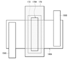
- FIG. 2 is a top view showing the configuration of the semiconductor device 100 according to the present embodiment.
- the semiconductor device 100 includes a substrate 110, a buffer layer 120, a channel layer 130, a low Ns region 131, a barrier layer 140, an ohmic layer 151, a source electrode 150S, and a drain electrode 150D.
- the first insulating layer 161 and the second insulating layer 162, the third insulating layer 163, the gate electrode 170, the gate insulating film 171 and the side opening region 172 are provided.
- the semiconductor device 100 is a high electron mobility transistor (HEMT) having a two-dimensional electron gas layer (2DEG) formed by the difference between the magnitude of the polarization of the channel layer 130 and the magnitude of the polarization of the barrier layer 140 as a channel.
- HEMT high electron mobility transistor
- 2DEG two-dimensional electron gas layer
- the two-dimensional electron gas layer is formed in, for example, the channel layer 130 in the vicinity of the barrier layer 140.
- the substrate 110 is a support for the semiconductor device 100.
- the substrate 110 may be a substrate made of a semiconductor material having a lattice constant close to that of the nitride semiconductor constituting the channel layer 130.
- the substrate 110 may be a substrate made of a III-V compound semiconductor such as a single crystal GaN substrate.
- the substrate 110 can be a substrate made of a material having a lattice constant different from that of the channel layer 130.
- the substrate 110 may be a SiC substrate, a sapphire substrate, a Si substrate, or the like.
- the buffer layer 120 is a nitride semiconductor layer epitaxially grown on the substrate 110.
- the buffer layer 120 can alleviate the lattice mismatch between the substrate 110 and the channel layer 130 by controlling the lattice constant of the surface on which the channel layer 130 is provided. According to this, the buffer layer 120 can improve the crystal state of the channel layer 130 and suppress the warp of the substrate 110.
- the buffer layer 120 may be composed of AlN, AlGaN, or GaN. However, depending on the configuration of the substrate 110 and the channel layer 130, the buffer layer 120 may not be provided.
- the buffer layer 120 may be provided in a single layer structure, or may be provided in a multilayer structure in which a plurality of AlN, AlGaN, or GaN is laminated. Further, when the buffer layer 120 is made of a ternary material such as AlGaN, the buffer layer 120 may be provided so that the composition gradually changes in the thickness direction.
- the channel layer 130 is composed of a nitride semiconductor having a narrower bandgap than the barrier layer 140.
- the channel layer 130 can accumulate carriers on the channel layer 130 side near the interface with the barrier layer 140 due to the difference in the magnitude of polarization from the barrier layer 140.
- the channel layer 130 may be composed of epitaxially grown GaN.
- the channel layer 130 may be composed of undoped u-GaN to which impurities are not added. In such a case, the channel layer 130 can suppress the scattering of impurities of the carriers, so that the mobility of the carriers can be further increased.
- the barrier layer 140 is composed of a nitride semiconductor having a wider bandgap than the channel layer 130.
- a nitride semiconductor having a wider bandgap than the channel layer 130.
- the barrier layer 140 may be composed of an epitaxially grown Al 1-xy Ga x In y N (where 0 ⁇ x ⁇ 1, 0 ⁇ y ⁇ 1). Further, the barrier layer 140 may be composed of an undoped u-Al 1-xy Ga x In y N to which impurities are not added. In such a case, the barrier layer 140 can suppress the scattering of impurities of the carriers in the channel layer 130, so that the mobility of the carriers can be further increased.
- the barrier layer 140 may be composed of a single layer, or may be configured by laminating a plurality of Al 1-xy Ga x In y N having different compositions. Further, the barrier layer 140 may be configured so that the composition gradually changes in the thickness direction.
- the low Ns region 131 is provided in a part of the channel layer 130 and has a lower carrier density than the other regions of the channel layer 130. Specifically, the low Ns region 131 is provided in a part of the channel layer 130 corresponding to the planar region in which the gate electrode 170 and the side opening region 172 are provided. The low Ns region 131 functions as part of the current path between the drain electrode 150D and the source electrode 150S.
- the low Ns region 131 Since the low Ns region 131 has a lower carrier density than the other regions of the channel layer 130, an excessive electric field is applied to the gate insulating film 171 between the low Ns region 131 and the gate electrode 170. It can be suppressed. Further, since the low Ns region 131 is provided so as to extend from the gate electrode 170 only by the side opening region 172, it is possible to suppress the occurrence of electric field concentration at the end of the gate electrode 170. Therefore, the low Ns region 131 can improve the withstand voltage of the semiconductor device 100.
- the laminated structure of the substrate 110, the buffer layer 120, the channel layer 130, and the barrier layer 140 is provided with an active region 140A surrounded by an insulating element separation region.
- the active region 140A is a region in which each configuration of the semiconductor device 100 is provided, and is provided as an island-shaped region surrounded by an element separation region.
- the device separation region is provided by inactivating the channel layer 130 and the barrier layer 140 by implanting ions such as B (boron).
- the element separation region is provided so as to surround the active region 140A, and electrically separates the active regions 140A from each other.
- the element separation region may be formed by removing the channel layer 130 and the barrier layer 140 by etching.
- a source electrode 150S and a drain electrode 150D are provided in the extending direction of the active region 140A, and a gate electrode 170 is provided between the source electrode 150S and the drain electrode 150D.
- the source electrode 150S and the drain electrode 150D may be provided so as to project from each other in a direction orthogonal to the extending direction of the active region 140A.
- the gate electrode 170 may be provided so as to cross the active region 140A in a direction orthogonal to the extending direction of the active region 140A.
- the ohmic layer 151 is provided on both sides of the barrier layer 140 with the gate electrode 170 interposed therebetween.
- the ohmic layer 151 forms an ohmic contact with the barrier layer 140 by heat treatment, thereby reducing the contact resistance between the source electrode 150S and the drain electrode 150D provided on the upper layer and the two-dimensional electron gas layer (2DEG). be able to.
- the ohmic layer 151 may be provided, for example, in a structure in which Ti (titanium), Al (aluminum), Ni (nickel), and Au (gold) are sequentially laminated from the barrier layer 140 side.
- the source electrode 150S and the drain electrode 150D are provided on the ohmic layers 151 provided on both sides of the gate electrode 170, respectively.
- the source electrode 150S and the drain electrode 150D can be electrically connected to the two-dimensional electron gas layer (2DEG) in the channel layer 130 via the ohmic layer 151.
- the source electrode 150S and the drain electrode 150D may be provided in a structure in which Ti (titanium), Al (aluminum), Ni (nickel), and Au (gold) are sequentially laminated from the ohmic layer 151 side.
- a regrowth layer may be provided below the ohmic layer 151.
- the barrier layer 140 and the channel layer 130 are dug from the barrier layer 140 side to a region deeper than the interface between the barrier layer 140 and the channel layer 130, and the dug region is made of an n-type nitride semiconductor. It is provided by embedding.
- the regrowth layer may be provided by selectively epitaxially growing a nitride semiconductor containing an n-type impurity in a region corresponding to a source and a drain using a selection mask.
- the regrowth layer may be provided by epitaxially growing a nitride semiconductor containing an n-type impurity on the entire surface and then removing the deposits on the mask.
- the source electrode 150S and the drain electrode 150D can be electrically connected to the two-dimensional electron gas layer (2DEG) with lower resistance.
- the regrowth layer may be composed of GaN containing n-type impurities such as Si or Ge at 1.0 ⁇ 10 19 pieces / cm 3 or more.
- the regrowth layer may be composed of In 1-x Ga x N (0 ⁇ x ⁇ 1), which is easier to grow at a lower temperature than GaN.
- the first insulating layer 161 is provided with an insulating material so as to cover the barrier layer 140 and the ohmic layer 151. Specifically, the first insulating layer 161 is provided with a material having an insulating property with respect to the barrier layer 140, the ohmic layer 151, and the gate electrode 170. According to this, the first insulating layer 161 protects the surface of the barrier layer 140 from impurities such as ions and improves the interface with the barrier layer 140 to suppress deterioration of the characteristics of the semiconductor device 100. Can be done.
- the first insulating layer 161 may be made of Al 2 O 3 having a film thickness of about 50 nm.
- the first insulating layer 161 is provided with an opening 150H for providing the source electrode 150S and the drain electrode 150D, and is provided with a gate opening 170H for providing the gate electrode 170.
- the gate opening 170H provided in the first insulating layer 161 is provided so as to have a width larger than the gate opening 170H provided in the second insulating layer 162 because the side opening region 172 described later is provided.
- the second insulating layer 162 is provided with an insulating material so as to cover the first insulating layer 161.
- the second insulating layer 162 is provided with a material having an insulating property with respect to the first insulating layer 161, the gate electrode 170, and the gate insulating film 171.
- the second insulating layer 162 can protect the surface of the barrier layer 140 from impurities such as ions.
- the second insulating layer 162 may be made of SiO 2 having a film thickness of about 100 nm.
- the second insulating layer 162 is provided with an opening 150H for providing the source electrode 150S and the drain electrode 150D, and is provided with a gate opening 170H for providing the gate electrode 170.
- the gate opening 170H provided in the second insulating layer 162 is smaller in width than the gate opening 170H provided in the first insulating layer 161. Therefore, the second insulating layer 162 is provided so as to protrude from the first insulating layer 161 inside the gate opening 170H.
- the gate insulating film 171 is uniformly provided on the second insulating layer 162 with an insulating material along the shape of the opening 150H and the gate opening 170H. Specifically, the gate insulating film 171 is formed on the second insulating layer 162, the inner side surface of the opening 150H provided in the first insulating layer 161 and the second insulating layer 162, and the inner side surface of the gate opening 170H. It is uniformly provided on the bottom surface.
- the gate insulating film 171 is provided with a material having an insulating property with respect to the barrier layer 140 and the gate electrode 170.
- the gate insulating film 171 protects the surface of the barrier layer 140 from impurities such as ions and improves the interface with the barrier layer 140 to suppress deterioration of the characteristics of the semiconductor device 100.
- the gate insulating film 171 may be provided as a single-layer film or a laminated film with Al 2 O 3 or HfO 2 having a film thickness of about 10 nm.
- the gate electrode 170 is made of a conductive material and is provided on the gate insulating film 171 inside the gate opening 170H. Specifically, the gate electrode 170 is provided on the gate insulating film 171 on the barrier layer 140 through the gate opening 170H from above the second insulating layer 162. For example, the gate electrode 170 may be provided by laminating Ni (nickel) and Au (gold) from the gate insulating film 171 side.
- the gate electrode 170 can control the carrier concentration of the two-dimensional electron gas layer (2DEG) formed in the channel layer 130 by the applied voltage. Specifically, the gate electrode 170 controls the thickness of the depletion layer formed in the lower barrier layer 140 by the applied voltage, so that the carrier concentration of the two-dimensional electron gas layer (2DEG) formed in the channel layer 130 is controlled. Can be controlled by the electric field effect.
- the side opening region 172 is provided at least on one side of the side surface of the gate electrode 170 between the source electrode 150S or the drain electrode 150D and the gate electrode 170 as a side opening with respect to the first insulating layer 161.
- the side opening region 172 can form a low Ns region 131 in the channel layer 130 by processing the barrier layer 140 via the side opening region 172 and the gate opening 170H. That is, the low Ns region 131 is provided in the channel layer 130 in the plane region where the side opening region 172 and the gate electrode 170 are provided.
- the low Ns region 131 can be formed by recessing, adding a fixed charge, anion doping, or the like to the barrier layer 140 exposed at the side opening region 172 and the gate opening 170H.
- the side opening region 172 may be provided at least on the side surface of the gate electrode 170 between the drain electrode 150D and the gate electrode 170. Electric field concentration at the end of the gate electrode 170 tends to occur on the drain electrode 150D side. Therefore, the side opening region 172 can improve the pressure resistance at the end of the gate electrode 170 by forming the low Ns region 131 on the drain electrode 150D side.
- the side opening region 172 may be provided on both sides of the side surface of the gate electrode 170 between the source electrode 150S and the drain electrode 150D and the gate electrode 170, respectively. According to this, the side opening region 172 can further improve the pressure resistance at the end of the gate electrode 170 by forming the low Ns region 131 on each side of the source electrode 150S and the drain electrode 150D.
- the side opening region 172 provided on the drain electrode 150D side may be provided with a width larger than the side opening region 172 provided on the source electrode 150S side.
- the electric field concentration at the end of the gate electrode 170 tends to occur on the drain electrode 150D side. Therefore, the semiconductor device 100 can further improve the withstand voltage by providing the side opening region 172 and the low Ns region 131 on the drain electrode 150D side with a larger width.
- the side opening region 172 may be provided over the entire side surface of the gate electrode 170.
- a gate opening 170H penetrating the first insulating layer 161 and the second insulating layer 162 is formed by dry etching, and the side surface of the first insulating layer 161 exposed by the gate opening 170H is wetted. It is formed by removing it by etching.
- the side opening region 172 is provided so as to extend from the gate opening 170H to the entire circumference. Since the side opening region 172 can form the low Ns region 131 in the active region 140A directly below, it is possible to suppress excessive electric field application and electric field concentration between the low Ns region 131 and the gate electrode 170. can.
- the third insulating layer 163 is provided on the gate insulating film 171 with an insulating material.
- the third insulating layer 163 is provided with a material having an insulating property with respect to the source electrode 150S, the drain electrode 150D, and the gate electrode 170.
- the third insulating layer 163 may be made of SiO 2 or Si 3 N 4 or the like.
- the third insulating layer 163 is provided with an opening 150H for providing the source electrode 150S and the drain electrode 150D.
- the semiconductor device 100 improves the gate withstand voltage of the semiconductor device 100 by providing a low Ns region 131 with a reduced carrier density in a part of the channel layer 130. be able to.
- the size of the low Ns region 131 and the degree of reduction of the carrier density of the low Ns region 131 can be appropriately set according to the specifications of the semiconductor device 100. However, further expansion of the low Ns region 131 and further reduction of the carrier density of the low Ns region 131 may further improve the withstand voltage of the semiconductor device 100, while increasing the on-resistance of the semiconductor device 100. There is.
- FIG. 3 and FIG. 3 show the suitable size of the low Ns region 131 capable of achieving both the withstand voltage of the semiconductor device 100 and the on-resistance, and the suitable reduction degree of the carrier density of the low Ns region 131. This will be specifically described with reference to FIG.
- FIG. 3 is an enlarged vertical sectional view of the vicinity of the gate electrode 170 and the side opening region 172 of FIG.
- the width w of the side opening region 172 is preferably 0.3 Lg or more and 0.4 Lg or less from the gate electrode 170, and is a low Ns region.
- the width w5 of 131 is preferably 1.6 Lg or more and 1.8 Lg or less.
- the barrier layer 140 is composed of AlInN having an In concentration of 19%
- the side opening region 172 and the low Ns region 131 are provided in the above range to improve the pressure resistance of the semiconductor device 100 while improving the pressure resistance. It is possible not to increase the on-resistance excessively.
- the width w of the side opening region 172 is preferably 100 nm or less from the gate electrode 170, and the low Ns region 131 is a region protruding from the gate electrode 170 on both sides of the source electrode 150S and the drain electrode 150D at 100 nm or less, respectively. It is preferable to be provided in.
- the side opening region 172 is provided with a width within the above range, and the low Ns region 131 is formed in an appropriate range to obtain a withstand voltage of the semiconductor device 100. It is possible not to increase the on-resistance excessively while improving the property.
- the lower limit of the width of the side opening region 172 is not particularly limited, but may be 10 nm from the viewpoint of difficulty in forming the side opening region 172 and cost.
- the degree of reduction of the carrier density in the low Ns region 131 can be appropriately set according to the specifications of the semiconductor device 100.
- the carrier density of the low Ns region 131 is preferably 50% or more and 90% or less with respect to the carrier density of the other regions of the channel layer 130. In such a case, the semiconductor device 100 can improve the withstand voltage and suppress an excessive increase in on-resistance.
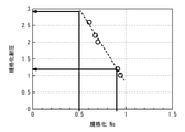
- FIG. 4 is a graph showing the relationship between the carrier density (Ns) of the low Ns region 131 and the withstand voltage of the semiconductor device 100.
- the measurement results of the withstand voltage of each of the semiconductor devices 100 manufactured by varying the carrier density (Ns) of the low Ns region 131 are shown in the carrier density of the semiconductor device 100 including the low Ns region 131 having the highest carrier density.
- the withstand voltage are shown as standardized values set to 1 respectively.
- the withstand voltage was shown by the gate voltage when the drain current Id-gate voltage Vg of the semiconductor device 100 was evaluated and the Id waveform exceeded the threshold value. For example, when the drain voltage Vd is fixed at 0.1 V and the gate voltage Vg is scanned in the off direction, the gate voltage when the drain current Id exceeds 1 ⁇ 10 -6 mA / mm is shown as the withstand voltage.
- the withstand voltage of the semiconductor device 100 increases by reducing the carrier density of the low Ns region 131 by 10%. Further, it can be seen that the withstand voltage of the semiconductor device 100 increases to about 3 times by reducing the carrier density of the low Ns region 131 by 50%. As can be seen from the graph shown in FIG. 4, the increase in the withstand voltage of the semiconductor device 100 with respect to the decrease in the carrier density in the low Ns region 131 is linear. Therefore, the low Ns region 131 similarly reduces the carrier density by 10% or more and 50% or less with respect to the other regions of the channel layer 130 even in comparison with the other regions of the channel layer 130. It is considered that the withstand voltage of the semiconductor device 100 can be improved.
- the low Ns region 131 preferably has a carrier density of 50% or more and 90% or less with respect to the other regions of the channel layer 130. According to this, the semiconductor device 100 can improve the withstand voltage and suppress an excessive increase in on-resistance.
- the barrier layer 140 is composed of AlInN having an In concentration of 19%, by setting the carrier density of the low Ns region 131 within the above range, it is possible to more preferably achieve both the withstand voltage and the on-resistance of the semiconductor device 100. can.
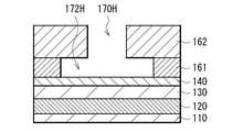
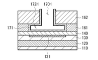
- FIGS. 5A to 5G are vertical cross-sectional views illustrating one step of the manufacturing method of the semiconductor device 100 according to the present embodiment.
- a channel layer 130 is formed by epitaxially growing a buffer layer 120 on a substrate 110 made of, for example, Si, and then epitaxially growing GaN. Subsequently, the barrier layer 140 is formed by epitaxially growing AlGaN (Al 0.3- Ga 0.7 N mixed crystal) on the channel layer 130.
- the ohmic layer 151 (not shown) is formed and the element separation region is formed.
- the ohmic layer 151 is formed on the barrier layers 140 on both sides of the region where the gate electrode 170 is formed in the subsequent stage, and an annealing treatment is performed to electrically connect the barrier layer 140 to the barrier layer 140 with low contact resistance.
- Ohmic layer 151 is formed. It is also possible to provide a re-growth layer in which the n-type nitride semiconductor is selectively re-growth under the ohmic layer 151.
- an element separation region in which the barrier layer 140 and the channel layer 130 have high resistance is formed.
- the element separation region is formed so as to surround the island-shaped active region 140A, for example, and electrically separates the active regions 140A from each other.
- the formation of the element separation region may be performed at an arbitrary timing such as after the formation of the gate electrode 170.
- the first insulating layer 161 is formed by depositing Al 2 O 3 (aluminum oxide) on the barrier layer 140 using the ALD (Atomic Layer Deposition) method. Further, the second insulating layer 162 is formed by depositing SiO 2 (silicon oxide) on the first insulating layer 161 using a CVD (Chemical Vapor Deposition) method.
- a gate opening 170H that exposes the first insulating layer 161 is formed.
- the gate opening 170H can be formed by further suppressing the expansion of the opening width.
- the barrier layer 140 may be damaged in the subsequent process.
- the etching selectivity between the first insulating layer 161 and the second insulating layer 162 is 1 or more, preferably 5 or more, excessive etching to the first insulating layer 161 is suppressed, so that the barrier layer 140 is reached. Damage can be suppressed.
- the first insulating layer 161 is wet-etched to form a side opening 172H on the side surface of the first insulating layer 161 exposed at the gate opening 170H.
- the etching selectivity between the first insulating layer 161 and the second insulating layer 162 is 1 or more, preferably 5 or more
- the first insulating layer 161 is etched while proceeding in the side surface direction. 2 It is possible to suppress the progress of etching on the insulating layer 162. According to this, it is possible to prevent the opening width of the gate opening 170H formed in the second insulating layer 162 from widening due to the wet etching of the first insulating layer 161.
- the low Ns region 131 is formed in the channel layer 130 by recessing the barrier layer 140 exposed at the gate opening 170H and the side opening 172H.
- the self-polarization of the barrier layer 140 a mixture of self-polarization and piezo-polarization depending on the material
- the low Ns region 131 can be formed in the channel layer 130 in the region where the barrier layer 140 is recessed.
- the recess of the barrier layer 140 can be realized, for example, by performing oxidation and wet etching on the barrier layer 140.
- the low Ns region 131 is formed in the channel layer 130 by using the gate opening 170H and the side opening 172H, it is possible to form the low Ns region 131 without adding a mask or the like.
- the end of the low Ns region 131 may coincide with the end of the side opening 172H, or may extend outward from the end of the side opening 172H.
- the gate insulating film 171 is formed by depositing Al 2 O 3 (aluminum oxide) using the ALD (Atomic Layer Deposition) method. Since the ALD method can form a homogeneous film in the entire exposed region, the gate insulating film 171 includes a barrier layer 140 including the inside of the gate opening 170H and the side opening 172H, a first insulating layer 161 and a second. It is formed as a homogeneous film on the exposed surface of the insulating layer 162.
- the gate electrode 170 is formed by sequentially depositing Ni (nickel) and Au (gold) so as to embed the gate opening 170H on the gate insulating film 171. Then, after depositing the third insulating layer 163 on the gate insulating film 171 and forming the source electrode 150S and the drain electrode 150D on the ohmic layer 151 (not shown), the semiconductor device 100 according to the present embodiment is manufactured. can do.
- the side opening region 172 becomes a void, but it is also possible to embed a low dielectric constant material in the side opening region 172.
- a low dielectric constant material is deposited so as to embed the side opening 172H, and the low dielectric constant material deposited on the gate opening 170H is removed by anisotropic etching or the like. Therefore, the side opening region 172 can be embedded with a low dielectric constant material.
- the low Ns region 131 can be formed by a method other than that described with reference to FIG. 5E. A modification of the method for forming the low Ns region 131 will be described with reference to FIGS. 6 to 7B.
- FIG. 6 is a vertical cross-sectional view illustrating a modified example of the method for forming the low Ns region 131.
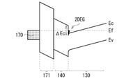
- FIG. 7A is an energy band diagram of the semiconductor device 100 before adding a fixed charge to the barrier layer 140.
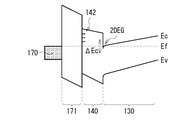
- FIG. 7B is an energy band diagram of the semiconductor device 100 after applying a fixed charge to the barrier layer 140.
- E c indicates the energy level at the lower end of the conduction band
- E v indicates the energy level at the upper end of the valence band
- E f indicates the Fermi level.
- the barrier layer 140 exposed at the gate opening 170H and the side opening 172H is oxidized (that is, ashed) with N 2 plasma or O 2 plasma and fixed to the barrier layer 140.
- the low Ns region 131 can be formed in the channel layer 130.
- the energy band of the channel layer 130 is lifted by the fixed charge 142 of the barrier layer 140, so that the channel layer 130 is used as a two-dimensional electron gas layer (2DEG).
- the accumulated carriers are reduced.
- the low Ns region 131 having a reduced carrier density can be formed in the channel layer 130 corresponding to the barrier layer 140 to which the fixed charge 142 is added. Therefore, the low Ns region 131 can be formed in the channel layer 130 corresponding to the barrier layer 140 exposed by the gate opening 170H and the side opening 172H.
- the low Ns region 131 is formed in the channel layer 130 by using the gate opening 170H and the side opening 172H, it is possible to form the low Ns region 131 without adding a mask or the like.
- the end of the low Ns region 131 may coincide with the end of the side opening 172H, or may extend outward from the end of the side opening 172H.
- FIG. 8 is a schematic perspective view showing the configuration of the semiconductor module 1 according to the second embodiment of the present disclosure.
- the semiconductor module 1 has, for example, an edge antenna 20 formed in an array and a front of a switch 10, a low noise amplifier 41, a bandpass filter 42, a power amplifier 43, and the like. It is an antenna integrated module in which the end parts are mounted as one module.
- the semiconductor module 1 can be used, for example, as a transceiver for wireless communication.
- the semiconductor module 1 includes, for example, the semiconductor device 100 according to the first embodiment as a transistor constituting a switch 10, a low noise amplifier 41, a power amplifier 43, or the like.
- the semiconductor module 1 that uses radio waves in a higher frequency band, the propagation loss of radio waves becomes larger, so the semiconductor module 1 that supports 5G transmits radio waves with higher power. It is desirable to do.
- the semiconductor module 1 including the semiconductor device 100 according to the first embodiment can further improve the withstand voltage, it is possible to perform high output, low power consumption, and high reliability wireless communication. That is, the semiconductor module 1 can be more preferably used for the 5th generation mobile communication (5G).
- FIG. 9 is a block diagram showing a configuration of the wireless communication device 2 according to the third embodiment of the present disclosure.
- the wireless communication device 2 includes an antenna ANT, an antenna switch circuit 3, a high power amplifier HPA, a high frequency integrated circuit RFIC (Radio Frequency Integrated Circuit), a base band unit BB, and an audio output unit. It includes a MIC, a data output unit DT, and an interface unit I / F (for example, wireless LAN (Wireless Local Area Network: W-LAN), Bluetooth (registered trademark), etc.).
- the wireless communication device 2 is a mobile phone system having multiple functions such as voice, data communication, and LAN connection.
- a transmission signal is output from the baseband portion BB to the antenna ANT via the high frequency integrated circuit RFIC, the high power amplifier HPA, and the antenna switch circuit 3 at the time of transmission. Further, in the wireless communication device 2, the received signal is input from the antenna ANT to the baseband portion BB via the antenna switch circuit 3 and the high frequency integrated circuit RFIC at the time of reception.
- the received signal processed by the baseband unit BB is output to the outside of the wireless communication device 2 from, for example, the voice output unit MIC, the data output unit DT, or the interface unit I / F.
- the wireless communication device 2 includes the semiconductor device 100 according to the first embodiment as a transistor constituting the antenna switch circuit 3, the high power amplifier HPA, the high frequency integrated circuit RFIC, the baseband portion BB, and the like. According to this, since the wireless communication device 2 can further improve the withstand voltage, it is possible to perform high output, low power consumption, and highly reliable wireless communication.
- the semiconductor device 100 is composed of a GaN-based compound semiconductor, but the technique according to the present disclosure is not limited to the above examples.
- the semiconductor device 100 may be composed of a GaAs-based compound semiconductor.
- the technology according to the present disclosure may have the following configuration. According to the technique according to the present disclosure having the following configuration, it is possible to form a low Ns region with a reduced carrier density in the channel layer corresponding to the barrier layer exposed by the gate opening and the side opening region. Therefore, in the semiconductor device, the electric field generated between the gate electrode and the channel layer can be relaxed by the low Ns region, so that the gate withstand voltage can be further increased.
- the effects exerted by the techniques according to the present disclosure are not necessarily limited to the effects described herein, and may be any of the effects described in the present disclosure.
- an insulating layer to be embedded between the gate electrode and the source electrode or the drain electrode is provided.
- the low Ns region is provided in the channel layer directly below the gate electrode and the side opening region.
- the carrier density in the low Ns region is 50% or more and 90% or less with respect to the carrier density in the other regions of the channel layer. .. (6)
- the semiconductor device according to any one of (1) to (10) above, wherein the barrier layer contains AlInN as the second nitride semiconductor.
- (12) Equipped with semiconductor devices, The semiconductor device is A channel layer containing a first nitride semiconductor and A barrier layer containing a second nitride semiconductor and provided on the channel layer, The source electrode and the drain electrode provided on the barrier layer, and A gate electrode provided on the barrier layer between the source electrode and the drain electrode, A side opening region provided at least on one side of the side surface of the gate electrode between the source electrode or the drain electrode and the gate electrode.
- a semiconductor module comprising at least a low Ns region provided in the channel layer corresponding to a planar region provided with the gate electrode and the side opening region and having a lower carrier density than the other regions of the channel layer.
- the semiconductor device is A channel layer containing a first nitride semiconductor and A barrier layer containing a second nitride semiconductor and provided on the channel layer, The source electrode and the drain electrode provided on the barrier layer, and A gate electrode provided on the barrier layer between the source electrode and the drain electrode, A side opening region provided at least on one side of the side surface of the gate electrode between the source electrode or the drain electrode and the gate electrode.
- a wireless communication device including at least a low Ns region provided in the channel layer corresponding to a planar region provided with the gate electrode and the side opening region and having a lower carrier density than other regions of the channel layer.
Landscapes
- Junction Field-Effect Transistors (AREA)
Abstract
第1窒化物半導体を含むチャネル層と、第2窒化物半導体を含み、前記チャネル層の上に設けられたバリア層と、前記バリア層の上に設けられたソース電極及びドレイン電極と、前記ソース電極及び前記ドレイン電極の間の前記バリア層の上に設けられたゲート電極と、前記ソース電極又は前記ドレイン電極と、前記ゲート電極との間の前記ゲート電極の側面の片側に少なくとも設けられた側面開口領域と、前記ゲート電極及び前記側面開口領域が設けられた平面領域に対応して前記チャネル層に設けられ、前記チャネル層の他の領域よりもキャリア密度が低い低Ns領域とを備える、半導体装置。
Description
本開示は、半導体装置、半導体モジュール、及び無線通信装置に関する。
近年、化合物半導体のヘテロ接合の界面に形成される二次元電子ガス層をチャネルとする高電子移動度トランジスタ(High Electron Mobility Transistor:HEMT)が提案されている。
二次元電子ガス層は、電子の移動度が高く、かつシート電子密度が高いため、二次元電子ガス層をチャネルとするHEMTは、低抵抗、高耐圧、かつ高速動作が可能なトランジスタとして期待されている。例えば、HEMTは、パワーデバイス又はRF(Radio Frequency)デバイスなどへの適用が期待されている。
例えば、化合物半導体層と、ゲートメタルとがゲート絶縁膜を介して接合するMIS(Metal-Insulator-Semiconductor)構造のHEMTが提案されている(例えば、特許文献1)。MIS構造のHEMTでは、化合物半導体層とゲートとの界面にゲート絶縁膜が存在し、オフ動作時のゲートリークが抑制されるため、消費電力を低減することができる。したがって、MIS構造のHEMTは、携帯可能な無線通信装置に好適であると期待されている。
一般的に、MIS構造のトランジスタは、ゲート絶縁膜を薄膜化することで、さらなる高速動作を実現することができる。一方で、ゲート絶縁膜の薄膜化は、ゲート絶縁膜の絶縁耐圧を低下させるため、オフ動作時のゲート耐圧を低下させる可能性がある。
MIS型のHEMTでは、チャネルである二次元電子ガス層のキャリア密度が高いため、ゲート絶縁膜により高い電界が印加されやすい。そのため、HEMTでは、ゲート耐圧をより向上させることが望まれる。
耐圧性がより向上した半導体装置、並びに該半導体装置を備える半導体モジュール及び無線通信装置が提供されることが望ましい。
本開示の一実施形態に係る半導体装置は、第1窒化物半導体を含むチャネル層と、第2窒化物半導体を含み、前記チャネル層の上に設けられたバリア層と、前記バリア層の上に設けられたソース電極及びドレイン電極と、前記ソース電極及び前記ドレイン電極の間の前記バリア層の上に設けられたゲート電極と、前記ソース電極又は前記ドレイン電極と、前記ゲート電極との間の前記ゲート電極の側面の片側に少なくとも設けられた側面開口領域と、前記ゲート電極及び前記側面開口領域が設けられた平面領域に対応して前記チャネル層に設けられ、前記チャネル層の他の領域よりもキャリア密度が低い低Ns領域とを備える。
本開示の一実施形態に係る半導体モジュールは、半導体装置を備え、前記半導体装置は、第1窒化物半導体を含むチャネル層と、第2窒化物半導体を含み、前記チャネル層の上に設けられたバリア層と、前記バリア層の上に設けられたソース電極及びドレイン電極と、前記ソース電極及び前記ドレイン電極の間の前記バリア層の上に設けられたゲート電極と、前記ソース電極又は前記ドレイン電極と前記ゲート電極との間の前記ゲート電極の側面の片側に少なくとも設けられた側面開口領域と、前記ゲート電極及び前記側面開口領域が設けられた平面領域に対応する前記チャネル層に少なくとも設けられ、前記チャネル層の他の領域よりもキャリア密度が低い低Ns領域とを含む。
本開示の一実施形態に係る無線通信装置は、半導体装置を備え、前記半導体装置は、第1窒化物半導体を含むチャネル層と、第2窒化物半導体を含み、前記チャネル層の上に設けられたバリア層と、前記バリア層の上に設けられたソース電極及びドレイン電極と、前記ソース電極及び前記ドレイン電極の間の前記バリア層の上に設けられたゲート電極と、前記ソース電極又は前記ドレイン電極と前記ゲート電極との間の前記ゲート電極の側面の片側に少なくとも設けられた側面開口領域と、前記ゲート電極及び前記側面開口領域が設けられた平面領域に対応する前記チャネル層に少なくとも設けられ、前記チャネル層の他の領域よりもキャリア密度が低い低Ns領域とを含む。
本開示の一実施形態に係る半導体装置、半導体モジュール、及び無線通信装置では、ゲート電極が設けられるゲート開口、及びゲート電極の側面の片側に少なくとも設けられた側面開口領域によって露出されたバリア層の分極等を制御することができる。よって、該バリア層に対応するチャネル層にキャリア密度が低減された低Ns領域を形成することができる。
以下、本開示における実施形態について、図面を参照して詳細に説明する。以下で説明する実施形態は本開示の一具体例であって、本開示にかかる技術が以下の態様に限定されるわけではない。また、本開示の各構成要素の配置、寸法、及び寸法比等についても、各図に示す様態に限定されるわけではない。
なお、説明は以下の順序で行う。
1.第1の実施形態
1.1.構成例
1.2.製造方法
2.第2の実施形態
3.第3の実施形態
1.第1の実施形態
1.1.構成例
1.2.製造方法
2.第2の実施形態
3.第3の実施形態
<1.第1の実施形態>
(1.1.構成例)
まず、図1及び図2を参照して、本開示の第1の実施形態に係る半導体装置の構成について説明する。図1は、本実施形態に係る半導体装置100の構成を示す縦断面図である。図2は、本実施形態に係る半導体装置100の構成を示す上面図である。
(1.1.構成例)
まず、図1及び図2を参照して、本開示の第1の実施形態に係る半導体装置の構成について説明する。図1は、本実施形態に係る半導体装置100の構成を示す縦断面図である。図2は、本実施形態に係る半導体装置100の構成を示す上面図である。
図1に示すように、半導体装置100は、基板110と、バッファ層120と、チャネル層130と、低Ns領域131と、バリア層140と、オーミック層151と、ソース電極150Sと、ドレイン電極150Dと、第1絶縁層161と、第2絶縁層162と、第3絶縁層163と、ゲート電極170と、ゲート絶縁膜171と、側面開口領域172とを備える。
すなわち、半導体装置100は、チャネル層130の分極の大きさと、バリア層140の分極の大きさとの差によって形成された二次元電子ガス層(2DEG)をチャネルとする高電子移動度トランジスタ(HEMT)である。二次元電子ガス層は、例えば、バリア層140近傍のチャネル層130に形成される。
基板110は、半導体装置100の支持体である。具体的には、基板110は、チャネル層130を構成する窒化物半導体と格子定数が近い半導体材料で構成された基板であってもよい。例えば、基板110は、単結晶GaN基板などのIII-V族化合物半導体で構成された基板であってもよい。
なお、半導体装置100では、バッファ層120が設けられるため、基板110は、チャネル層130と格子定数が異なる材料で構成された基板とすることも可能である。例えば、基板110は、SiC基板、サファイア基板、又はSi基板などであってもよい。
バッファ層120は、基板110の上にエピタキシャル成長された窒化物半導体層である。バッファ層120は、チャネル層130が設けられる面の格子定数を制御することで、基板110と、チャネル層130との間の格子不整合を緩和することができる。これによれば、バッファ層120は、チャネル層130の結晶状態をより良好にするとともに、基板110の反りを抑制することができる。例えば、基板110が単結晶Si基板であり、チャネル層130がGaN層である場合、バッファ層120は、AlN、AlGaN、又はGaNで構成されてもよい。ただし、基板110及びチャネル層130の構成によっ
ては、バッファ層120は設けられなくともよい。
ては、バッファ層120は設けられなくともよい。
バッファ層120は、単層構造で設けられてもよく、AlN、AlGaN、又はGaNを複数積層した多層構造で設けられてもよい。また、バッファ層120がAlGaNなどの三元系材料で構成される場合、バッファ層120は、厚み方向に徐々に組成が変化するように設けられてもよい。
チャネル層130は、バリア層140よりもバンドギャップが狭い窒化物半導体で構成される。チャネル層130は、バリア層140との分極の大きさの差により、バリア層140との界面付近のチャネル層130側にキャリアを蓄積することができる。例えば、チャネル層130は、エピタキシャル成長されたGaNで構成されてもよい。また、チャネル層130は、不純物が添加されていないアンドープのu-GaNで構成されてもよい。このような場合、チャネル層130は、キャリアの不純物散乱を抑制することができるため、キャリアの移動度をより高めることができる。
バリア層140は、チャネル層130よりもバンドギャップが広い窒化物半導体で構成される。バリア層140は、チャネル層130と接合されることで、自発分極又はピエゾ分極によってバリア層140近傍のチャネル層130にキャリアを蓄積させることができる。これにより、チャネル層130のバリア層140近傍に高移動度かつ高キャリア濃度の二次元電子ガス層(2DEG)が形成される。
例えば、バリア層140は、エピタキシャル成長されたAl1-x-yGaxInyN(ただし、0≦x<1、0≦y<1)で構成されてもよい。また、バリア層140は、不純物が添加されていないアンドープのu-Al1-x-yGaxInyNで構成されてもよい。このような場合、バリア層140は、チャネル層130におけるキャリアの不純物散乱を抑制することができるため、キャリアの移動度をより高めることができる。
なお、バリア層140は、単層で構成されてもよく、組成が異なるAl1-x-yGaxInyNを複数積層することで構成されてもよい。また、バリア層140は、厚み方向に徐々に組成が変化するように構成されてもよい。
低Ns領域131は、チャネル層130の一部領域に設けられ、チャネル層130の他の領域よりもキャリア密度が低い領域である。具体的には、低Ns領域131は、ゲート電極170及び側面開口領域172が設けられた平面領域に対応するチャネル層130の一部領域に設けられる。低Ns領域131は、ドレイン電極150Dと、ソース電極150Sとの間の電流パスの一部として機能する。
低Ns領域131は、チャネル層130の他の領域よりもキャリア密度が低減されているため、低Ns領域131とゲート電極170との間でゲート絶縁膜171に過度の電界が印加されることを抑制することができる。また、低Ns領域131は、側面開口領域172だけゲート電極170から広がって設けられることにより、ゲート電極170の端部にて電界集中が生じることを抑制することができる。したがって、低Ns領域131は、半導体装置100の耐圧性を向上させることができる。
また、図2に示すように、基板110、バッファ層120、チャネル層130、及びバリア層140の積層構造体には、絶縁性の素子分離領域で囲まれたアクティブ領域140Aが設けられる。
アクティブ領域140Aは、半導体装置100の各構成が設けられる領域であり、素子分離領域に囲まれた島状の領域として設けられる。素子分離領域は、B(ホウ素)などの
イオン注入によってチャネル層130及びバリア層140を不活性化することで設けられる。素子分離領域は、アクティブ領域140Aを囲むように設けられ、アクティブ領域140Aを互いに電気的に分離する。なお、素子分離領域は、エッチングによるチャネル層130及びバリア層140の除去によって形成されてもよい。
イオン注入によってチャネル層130及びバリア層140を不活性化することで設けられる。素子分離領域は、アクティブ領域140Aを囲むように設けられ、アクティブ領域140Aを互いに電気的に分離する。なお、素子分離領域は、エッチングによるチャネル層130及びバリア層140の除去によって形成されてもよい。
アクティブ領域140Aには、アクティブ領域140Aの延在方向にソース電極150S及びドレイン電極150Dが設けられ、ソース電極150S及びドレイン電極150Dの間にゲート電極170が設けられる。具体的には、ソース電極150S及びドレイン電極150Dは、アクティブ領域140Aの延在方向と直交する方向に互いに反対側に突出するように設けられてもよい。ゲート電極170は、アクティブ領域140Aの延在方向と直交する方向にアクティブ領域140Aを横断するように設けられてもよい。
オーミック層151は、バリア層140の上にゲート電極170を挟んで両側に設けられる。オーミック層151は、熱処理によってバリア層140との間でオーミックコンタクトを形成することで、上層に設けられるソース電極150S及びドレイン電極150Dと、二次元電子ガス層(2DEG)との接触抵抗を低減することができる。オーミック層151は、例えば、バリア層140側からTi(チタン)、Al(アルミニウム)、Ni(ニッケル)、及びAu(金)を順次積層した構造で設けられてもよい。
ソース電極150S及びドレイン電極150Dは、ゲート電極170を挟んで両側に設けられたオーミック層151の上にそれぞれ設けられる。ソース電極150S及びドレイン電極150Dは、オーミック層151を介して、チャネル層130内の二次元電子ガス層(2DEG)と電気的に接続することができる。ソース電極150S及びドレイン電極150Dは、オーミック層151側からTi(チタン)、Al(アルミニウム)、Ni(ニッケル)、及びAu(金)を順次積層した構造で設けられてもよい。
なお、オーミック層151の下には、再成長層が設けられてもよい。再成長層は、例えば、バリア層140側からバリア層140とチャネル層130との界面よりも深い領域までバリア層140及びチャネル層130を掘り込み、掘り込んだ領域をn型窒化物半導体にて埋め込むことで設けられる。
具体的には、再成長層は、選択マスクを用いて、ソース及びドレインに対応する領域にn型不純物を含む窒化物半導体を選択的にエピタキシャル成長させることで設けられてもよい。または、再成長層は、n型不純物を含む窒化物半導体を全面にエピタキシャル成長させた後、マスク上の堆積物を除去することで設けられてもよい。
再成長層は、バリア層140よりも高い導電性を有するため、ソース電極150S及びドレイン電極150Dと、二次元電子ガス層(2DEG)とをより低抵抗で電気的に接続することができる。例えば、再成長層は、Si又はGeなどのn型不純物を1.0×10¹⁹個/cm3以上で含むGaNにて構成されてもよい。または、再成長層は、GaNよりも低温成長させやすいIn1-xGaxN(0≦x<1)にて構成されてもよい。
第1絶縁層161は、バリア層140及びオーミック層151を覆うように絶縁性材料にて設けられる。具体的には、第1絶縁層161は、バリア層140、オーミック層151、及びゲート電極170に対して絶縁性を有する材料にて設けられる。これによれば、第1絶縁層161は、イオンなどの不純物からバリア層140の表面を保護するとともに、バリア層140との界面を良好にすることで半導体装置100の特性の低下を抑止することができる。例えば、第1絶縁層161は、膜厚50nm程度のAl2O3にて構成されてもよい。
また、第1絶縁層161には、ソース電極150S及びドレイン電極150Dを設けるための開口150Hが設けられると共に、ゲート電極170を設けるためのゲート開口170Hが設けられる。第1絶縁層161に設けられるゲート開口170Hは、後述する側面開口領域172が設けられるために、第2絶縁層162に設けられるゲート開口170Hよりも幅が大きくなるように設けられる。
第2絶縁層162は、第1絶縁層161を覆うように絶縁性材料にて設けられる。第2絶縁層162は、第1絶縁層161、ゲート電極170、及びゲート絶縁膜171に対して絶縁性を有する材料にて設けられる。これによれば、第2絶縁層162は、イオンなどの不純物からバリア層140の表面を保護することができる。例えば、第2絶縁層162は、膜厚100nm程度のSiO2にて構成されてもよい。
また、第2絶縁層162には、ソース電極150S及びドレイン電極150Dを設けるための開口150Hが設けられると共に、ゲート電極170を設けるためのゲート開口170Hが設けられる。第2絶縁層162に設けられるゲート開口170Hは、第1絶縁層161に設けられるゲート開口170Hよりも幅が小さい。そのため、第2絶縁層162は、ゲート開口170Hの内部にて第1絶縁層161から突出するように設けられる。
ゲート絶縁膜171は、第2絶縁層162の上に開口150H及びゲート開口170Hの形状に沿って、絶縁性材料にて一様に設けられる。具体的には、ゲート絶縁膜171は、第2絶縁層162の上、第1絶縁層161及び第2絶縁層162に設けられた開口150Hの内部の側面、並びにゲート開口170Hの内部の側面及び底面に一様に設けられる。ゲート絶縁膜171は、バリア層140及びゲート電極170に対して絶縁性を有する材料で設けられる。これによれば、ゲート絶縁膜171は、イオンなどの不純物からバリア層140の表面を保護するとともに、バリア層140との界面を良好にすることで半導体装置100の特性の低下を抑止することができる。例えば、ゲート絶縁膜171は、膜厚10nm程度のAl2O3又はHfO2にて単層膜又は積層膜として設けられてもよい。
ゲート電極170は、導電性材料にてゲート開口170Hの内部のゲート絶縁膜171の上に設けられる。具体的には、ゲート電極170は、第2絶縁層162の上からゲート開口170Hを通って、バリア層140の上のゲート絶縁膜171の上に設けられる。例えば、ゲート電極170は、ゲート絶縁膜171側からNi(ニッケル)及びAu(金)を積層することで設けられてもよい。
ゲート電極170は、印加される電圧によって、チャネル層130に形成される二次元電子ガス層(2DEG)のキャリア濃度を制御することができる。具体的には、ゲート電極170は、下方のバリア層140に形成される空乏層の厚みを印加電圧によって制御することで、チャネル層130に形成される二次元電子ガス層(2DEG)のキャリア濃度を電界効果にて制御することができる。
側面開口領域172は、第1絶縁層161に対する側面開口として、ソース電極150S又はドレイン電極150Dと、ゲート電極170との間のゲート電極170の側面の片側に少なくとも設けられる。側面開口領域172は、側面開口領域172及びゲート開口170Hを介したバリア層140への処理によってチャネル層130に低Ns領域131を形成することができる。すなわち、側面開口領域172及びゲート電極170が設けられた平面領域のチャネル層130に低Ns領域131が設けられる。
例えば、低Ns領域131は、側面開口領域172及びゲート開口170Hにて露出されたバリア層140に対して、リセス、固定電荷の付加、又は陰イオンドーピングなどを
行うことで形成され得る。
行うことで形成され得る。
側面開口領域172は、ドレイン電極150Dと、ゲート電極170との間のゲート電極170の側面に少なくとも設けられてもよい。ゲート電極170の端部における電界集中は、ドレイン電極150D側で生じやすい。そのため、側面開口領域172は、ドレイン電極150D側に低Ns領域131を形成することで、ゲート電極170の端部における耐圧性を向上させることができる。
また、側面開口領域172は、ソース電極150S及びドレイン電極150Dと、ゲート電極170との間のゲート電極170の側面の両側にそれぞれ設けられてもよい。これによれば、側面開口領域172は、ソース電極150S及びドレイン電極150Dの各々の側に低Ns領域131を形成することで、ゲート電極170の端部における耐圧性をより向上させることができる。
なお、このような場合、ドレイン電極150D側に設けられた側面開口領域172は、ソース電極150S側に設けられた側面開口領域172よりも大きな幅で設けられてもよい。上述したようにゲート電極170の端部における電界集中は、ドレイン電極150D側で生じやすい。そのため、ドレイン電極150D側の側面開口領域172及び低Ns領域131がより大きな幅で設けられることにより、半導体装置100は、さらに耐圧性を向上させることができる。
また、図2に示すように、側面開口領域172は、ゲート電極170の側面全周に亘って設けられてもよい。例えば、側面開口領域172は、第1絶縁層161及び第2絶縁層162を貫通するゲート開口170Hをドライエッチングにて形成し、ゲート開口170Hにて露出された第1絶縁層161の側面をウェットエッチングにて除去することで形成される。このような場合、ウェットエッチングは等方的に進行するため、側面開口領域172は、ゲート開口170Hから全周に広がって設けられる。側面開口領域172は、直下のアクティブ領域140Aに低Ns領域131を形成することができるため、低Ns領域131とゲート電極170との間での過度の電界印加、及び電界集中を抑制することができる。
第3絶縁層163は、ゲート絶縁膜171の上に絶縁性材料にて設けられる。第3絶縁層163は、ソース電極150S、ドレイン電極150D、及びゲート電極170に対して絶縁性を有する材料にて設けられる。例えば、第3絶縁層163は、SiO2又はSi3N4などにて構成されてもよい。なお、第3絶縁層163には、ソース電極150S及びドレイン電極150Dを設けるための開口150Hが設けられる。
以上にて説明したように、本実施形態に係る半導体装置100は、チャネル層130の一部領域にキャリア密度が低減された低Ns領域131を設けることで、半導体装置100のゲート耐圧を向上させることができる。
低Ns領域131の大きさ、及び低Ns領域131のキャリア密度の低減度合いは、半導体装置100の仕様によって適宜設定することが可能である。ただし、低Ns領域131のさらなる拡大、及び低Ns領域131のキャリア密度のさらなる低減は、半導体装置100の耐圧性をより向上させることができる一方で、半導体装置100のオン抵抗を増加させる可能性がある。
以下では、半導体装置100の耐圧性と、オン抵抗とを良好に両立させることが可能な低Ns領域131の好適な大きさ、及び低Ns領域131のキャリア密度の好適な低減度合いについて図3及び図4を参照して具体的に説明する。
(低Ns領域131の好適な大きさ)
図3は、図1のゲート電極170及び側面開口領域172の近傍を拡大した縦断面図である。図3に示すように、ゲート電極170のゲート長w6がLgである場合、側面開口領域172の幅wは、ゲート電極170から0.3Lg以上0.4Lg以下となることが好ましく、低Ns領域131の幅w5は、1.6Lg以上1.8Lg以下となることが好ましい。特に、In濃度が19%のAlInNでバリア層140が構成される場合、側面開口領域172、及び低Ns領域131を上記範囲の幅で設けることで、半導体装置100の耐圧性を向上させつつ、オン抵抗を過度に高めないようにすることが可能である。
図3は、図1のゲート電極170及び側面開口領域172の近傍を拡大した縦断面図である。図3に示すように、ゲート電極170のゲート長w6がLgである場合、側面開口領域172の幅wは、ゲート電極170から0.3Lg以上0.4Lg以下となることが好ましく、低Ns領域131の幅w5は、1.6Lg以上1.8Lg以下となることが好ましい。特に、In濃度が19%のAlInNでバリア層140が構成される場合、側面開口領域172、及び低Ns領域131を上記範囲の幅で設けることで、半導体装置100の耐圧性を向上させつつ、オン抵抗を過度に高めないようにすることが可能である。
または、側面開口領域172の幅wは、ゲート電極170から100nm以下であることが好ましく、低Ns領域131は、ゲート電極170からソース電極150S及びドレイン電極150Dの両側にそれぞれ100nm以下で張り出した領域に設けられることが好ましい。特に、In濃度が19%のAlInNでバリア層140が構成される場合、側面開口領域172を上記範囲の幅で設け、低Ns領域131を適切な範囲に形成することで、半導体装置100の耐圧性を向上させつつ、オン抵抗を過度に高めないようにすることが可能である。なお、側面開口領域172の幅の下限値は、特に限定されないが、側面開口領域172の形成の難度及びコストの観点から10nmとしてもよい。
(低Ns領域131のキャリア密度の好適な低減度合い)
上述したように、低Ns領域131のキャリア密度の低減度合いは、半導体装置100の仕様に応じて適宜設定することが可能である。ただし、低Ns領域131のキャリア密度は、チャネル層130の他の領域のキャリア密度に対して50%以上90%以下であることが好ましい。このような場合、半導体装置100は、耐圧性を向上させると共に、オン抵抗の過度な上昇を抑制することができる。
上述したように、低Ns領域131のキャリア密度の低減度合いは、半導体装置100の仕様に応じて適宜設定することが可能である。ただし、低Ns領域131のキャリア密度は、チャネル層130の他の領域のキャリア密度に対して50%以上90%以下であることが好ましい。このような場合、半導体装置100は、耐圧性を向上させると共に、オン抵抗の過度な上昇を抑制することができる。
図4は、低Ns領域131のキャリア密度(Ns)と、半導体装置100の耐圧との関係を示すグラフ図である。図4では、低Ns領域131のキャリア密度(Ns)を変動させて製造した半導体装置100の各々の耐圧の測定結果を、キャリア密度が最も高かった低Ns領域131を備える半導体装置100のキャリア密度及び耐圧をそれぞれ1として規格化した値で示す。
なお、耐圧は、半導体装置100のドレイン電流Id-ゲート電圧Vg評価を実施し、Id波形が閾値を超えた際のゲート電圧にて示した。例えば、ドレイン電圧Vdを0.1Vで固定し、ゲート電圧Vgをオフ方向に走査した際にドレイン電流Idが1×10⁻⁶mA/mmを上回った際のゲート電圧を耐圧として示した。
図4に示すように、低Ns領域131のキャリア密度が10%低減されることで、半導体装置100の耐圧が上昇することがわかる。また、低Ns領域131のキャリア密度が50%低減されることで、半導体装置100の耐圧が3倍程度まで上昇することがわかる。図4に示すグラフ図からわかるように、低Ns領域131のキャリア密度の低減に対する半導体装置100の耐圧の上昇は線形的である。したがって、低Ns領域131は、チャネル層130の他の領域との比較であっても同様に、チャネル層130の他の領域に対してキャリア密度を10%以上50%以下で低減することで、半導体装置100の耐圧を向上させることができると考えられる。
したがって、低Ns領域131は、チャネル層130の他の領域に対して50%以上90%以下のキャリア密度を有することが好ましい。これによれば、半導体装置100は、耐圧性を向上させると共に、オン抵抗の過度な上昇を抑制することができる。特に、In濃度が19%のAlInNでバリア層140が構成される場合、低Ns領域131のキャリア密度を上記範囲とすることで、半導体装置100の耐圧及びオン抵抗をより好適に両立させることができる。
(1.2.製造方法)
続いて、図5A~図5Gを参照して、本実施形態に係る半導体装置100の製造方法について説明する。図5A~図5Gは、本実施形態に係る半導体装置100の製造方法の一工程を説明する縦断面図である。
続いて、図5A~図5Gを参照して、本実施形態に係る半導体装置100の製造方法について説明する。図5A~図5Gは、本実施形態に係る半導体装置100の製造方法の一工程を説明する縦断面図である。
まず、図5Aに示すように、例えば、Siなどで構成された基板110の上に、バッファ層120をエピタキシャル成長させた後、GaNをエピタキシャル成長させることでチャネル層130が形成される。続いて、チャネル層130の上にAlGaN(Al0.3-Ga0.7N混晶)をエピタキシャル成長させることでバリア層140が形成される。
その後、図示を省略したオーミック層151の形成、及び素子分離領域の形成が行われる。
具体的には、後段でゲート電極170が形成される領域の両側のバリア層140の上にオーミック層151を形成し、アニール処理を行うことで、バリア層140と低コンタクト抵抗で電気的に接続するオーミック層151が形成される。なお、オーミック層151の下にn型窒化物半導体を選択的に再成長させた再成長層を設けることも可能である。
また、バリア層140及びチャネル層130の所定の平面領域にB(ホウ素)をイオン注入することで、バリア層140及びチャネル層130を高抵抗化した素子分離領域が形成される。素子分離領域は、例えば、島状のアクティブ領域140Aの周囲を囲むように形成され、アクティブ領域140Aを互いに電気的に分離する。素子分離領域の形成は、ゲート電極170の形成の後など任意のタイミングで行われてもよい。
続いて、図5Bに示すように、ALD(Atomic Layer Deposition)法を用いてバリア層140の上にAl2O3(酸化アルミニウム)を堆積することで、第1絶縁層161が形成される。さらに、CVD(Chemical Vapor Deposition)法を用いて第1絶縁層161の上にSiO2(酸化シリコン)を堆積することで、第2絶縁層162が形成される。
次に、図5Cに示すように、第2絶縁層162をエッチングすることで、第1絶縁層161を露出させるゲート開口170Hが形成される。このとき、ドライエッチングを用いることで、ゲート開口170Hは、開口幅の広がりをより抑制して形成され得る。
なお、第2絶縁層162へのエッチングの際に第1絶縁層161が過度にエッチングされた場合、後段のプロセスにてバリア層140にダメージが入る可能性がある。第1絶縁層161と第2絶縁層162との間のエッチング選択比が1以上、好ましくは5以上である場合、第1絶縁層161への過度のエッチングが抑制されるため、バリア層140へのダメージを抑制することができる。
続いて、図5Dに示すように、第1絶縁層161をウェットエッチングすることで、ゲート開口170Hにて露出された第1絶縁層161の側面に側面開口172Hが形成される。このとき、第1絶縁層161と第2絶縁層162との間のエッチング選択比が1以上、好ましくは5以上である場合、第1絶縁層161の側面方向へのエッチングを進行させつつ、第2絶縁層162に対するエッチングの進行を抑制することができる。これによれば、第1絶縁層161のウェットエッチングによって、第2絶縁層162に形成されたゲート開口170Hの開口幅が広がってしまうことを抑制することができる。
次に、図5Eに示すように、ゲート開口170H及び側面開口172Hにて露出されたバリア層140をリセス(後退)させることで、チャネル層130に低Ns領域131が形成される。具体的には、バリア層140をリセスさせることで、バリア層140の自己分極(材料によっては自己分極及びピエゾ分極の混合)を弱めることができる。したがって、チャネル層130とバリア層140との分極の大きさの差に応じてチャネル層130に蓄積されるキャリア密度を低減することができる。これによれば、バリア層140をリセスさせた領域のチャネル層130に低Ns領域131を形成することができる。なお、バリア層140のリセスは、例えば、バリア層140に対して酸化及びウェットエッチングを行うことで実現することができる。
上記の方法では、ゲート開口170H及び側面開口172Hを用いてチャネル層130に低Ns領域131を形成するため、マスク等を追加することなく、低Ns領域131を形成することが可能である。なお、低Ns領域131の端部は、側面開口172Hの端部と一致していてもよく、側面開口172Hの端部より外側に広がっていてもよい。
続いて、図5Fに示すように、ALD(Atomic Layer Deposition)法を用いてAl2O3(酸化アルミニウム)を堆積することで、ゲート絶縁膜171が形成される。ALD法は、露出した領域全てに均質な膜を形成することができるため、ゲート絶縁膜171は、ゲート開口170H及び側面開口172Hの内部を含むバリア層140、第1絶縁層161、及び第2絶縁層162の露出面に均質な膜として形成される。
次に、図5Gに示すように、ゲート絶縁膜171の上にゲート開口170Hを埋め込むように、Ni(ニッケル)、及びAu(金)を順次堆積することでゲート電極170が形成される。その後、ゲート絶縁膜171の上に第3絶縁層163を堆積した後、図示されないオーミック層151の上にソース電極150S及びドレイン電極150Dを形成することで、本実施形態に係る半導体装置100を製造することができる。
なお、上記の製造方法では、側面開口領域172は空隙となるが、側面開口領域172に低誘電率材料を埋め込むことも可能である。具体的には、ゲート絶縁膜171の形成後に、側面開口172Hを埋め込むように低誘電率材料を堆積し、異方性エッチング等を用いてゲート開口170Hに堆積した低誘電率材料を除去することで、側面開口領域172を低誘電率材料で埋め込むことが可能である。
(変形例)
低Ns領域131は、図5Eを参照して説明した方法以外でも形成することが可能である。図6~図7Bを参照して、低Ns領域131の形成方法の変形例について説明する。図6は、低Ns領域131の形成方法の変形例を説明する縦断面図である。図7Aは、バリア層140に固定電荷を付加する前の半導体装置100のエネルギーバンド図である。図7Bは、バリア層140に固定電荷を付加した後の半導体装置100のエネルギーバンド図である。なお、図7A及び図7Bにおいて、Ecは伝導帯の下端のエネルギー準位を示し、Evは価電子帯の上端のエネルギー準位を示し、Efは、フェルミ準位を示す。
低Ns領域131は、図5Eを参照して説明した方法以外でも形成することが可能である。図6~図7Bを参照して、低Ns領域131の形成方法の変形例について説明する。図6は、低Ns領域131の形成方法の変形例を説明する縦断面図である。図7Aは、バリア層140に固定電荷を付加する前の半導体装置100のエネルギーバンド図である。図7Bは、バリア層140に固定電荷を付加した後の半導体装置100のエネルギーバンド図である。なお、図7A及び図7Bにおいて、Ecは伝導帯の下端のエネルギー準位を示し、Evは価電子帯の上端のエネルギー準位を示し、Efは、フェルミ準位を示す。
図6に示すように、ゲート開口170H及び側面開口172Hにて露出されたバリア層140に対して、N2プラズマ又はO2プラズマにて酸化処理(すなわち、アッシング)を行い、バリア層140に固定電荷142を発生させることで、チャネル層130に低Ns領域131を形成することができる。
具体的には、図7A及び図7Bを比較することで分かるように、バリア層140の固定
電荷142によってチャネル層130のエネルギーバンドが持ち上がるため、二次元電子ガス層(2DEG)としてチャネル層130に蓄積されたキャリアが減少する。これにより、固定電荷142を付加したバリア層140に対応するチャネル層130に、キャリア密度が低減された低Ns領域131を形成することができる。よって、ゲート開口170H及び側面開口172Hにて露出されたバリア層140に対応するチャネル層130に低Ns領域131を形成することができる。
電荷142によってチャネル層130のエネルギーバンドが持ち上がるため、二次元電子ガス層(2DEG)としてチャネル層130に蓄積されたキャリアが減少する。これにより、固定電荷142を付加したバリア層140に対応するチャネル層130に、キャリア密度が低減された低Ns領域131を形成することができる。よって、ゲート開口170H及び側面開口172Hにて露出されたバリア層140に対応するチャネル層130に低Ns領域131を形成することができる。
上記の方法では、ゲート開口170H及び側面開口172Hを用いてチャネル層130に低Ns領域131を形成するため、マスク等を追加することなく、低Ns領域131を形成することが可能である。なお、低Ns領域131の端部は、側面開口172Hの端部と一致していてもよく、側面開口172Hの端部より外側に広がっていてもよい。
<2.第2の実施形態>
続いて、図8を参照して、本開示の第2の実施形態に係る半導体モジュールについて説明する。図8は、本開示の第2の実施形態に係る半導体モジュール1の構成を示す模式的な斜視図である。
続いて、図8を参照して、本開示の第2の実施形態に係る半導体モジュールについて説明する。図8は、本開示の第2の実施形態に係る半導体モジュール1の構成を示す模式的な斜視図である。
図8に示すように、本実施形態に係る半導体モジュール1は、例えば、アレイ状に形成されたエッジアンテナ20と、スイッチ10、低ノイズアンプ41、バンドパスフィルタ42、及びパワーアンプ43等のフロントエンド部品とが1つのモジュールとして実装されたアンテナ一体型モジュールである。半導体モジュール1は、例えば、無線通信用のトランシーバとして用いられ得る。
半導体モジュール1は、例えば、スイッチ10、低ノイズアンプ41、又はパワーアンプ43等を構成するトランジスタとして第1の実施形態に係る半導体装置100を含む。例えば、より高い周波数帯域の電波を使用する第5世代移動体通信(5G)では、電波の伝搬損失がより大きくなってしまうため、5Gに対応した半導体モジュール1では、より高い電力で電波を送信することが望まれる。第1の実施形態に係る半導体装置100を含む半導体モジュール1は、耐圧性をより向上させることができるため、高出力、低消費電力、及び高信頼性の無線通信を行うことが可能である。すなわち、半導体モジュール1は、第5世代移動体通信(5G)に対してより好適に用いることが可能である。
<3.第3の実施形態>
次に、図9を参照して、本開示の第3の実施形態に係る無線通信装置について説明する。図9は、本開示の第3の実施形態に係る無線通信装置2の構成を示すブロック図である。
次に、図9を参照して、本開示の第3の実施形態に係る無線通信装置について説明する。図9は、本開示の第3の実施形態に係る無線通信装置2の構成を示すブロック図である。
図9に示すように、無線通信装置2は、アンテナANTと、アンテナスイッチ回路3と、高電力増幅器HPAと、高周波集積回路RFIC(Radio Frequency Integrated Circuit)と、ベースバンド部BBと、音声出力部MICと、データ出力部DTと、インタフェース部I/F(例えば、無線LAN(Wireless Local Area Network:W-LAN)、又はBluetooth(登録商標)など)とを備える。無線通信装置2は、例えば、音声、データ通信、及びLAN接続などの多機能を有する携帯電話システムである。
無線通信装置2では、送信時に、ベースバンド部BBから高周波集積回路RFIC、高電力増幅器HPA、及びアンテナスイッチ回路3を介してアンテナANTに送信信号が出力される。また、無線通信装置2では、受信時に、アンテナANTからアンテナスイッチ回路3及び高周波集積回路RFICを介してベースバンド部BBに受信信号が入力される。ベースバンド部BBにて処理された受信信号は、例えば、音声出力部MIC、データ出
力部DT、又はインタフェース部I/Fから無線通信装置2の外部に出力される。
力部DT、又はインタフェース部I/Fから無線通信装置2の外部に出力される。
無線通信装置2は、アンテナスイッチ回路3、高電力増幅器HPA、高周波集積回路RFIC、又はベースバンド部BB等を構成するトランジスタとして第1の実施形態に係る半導体装置100を含む。これによれば、無線通信装置2は、耐圧性をより向上させることができるため、高出力、低消費電力、及び高信頼性の無線通信を行うことが可能である。
以上、実施形態を挙げて、本開示にかかる技術を説明した。ただし、本開示にかかる技術は、上記実施形態等に限定されるわけではなく、種々の変形が可能である。
例えば、上記実施形態では、半導体装置100は、GaN系化合物半導体にて構成される例を示したが、本開示に係る技術は、上記例示に限定されない。例えば、半導体装置100は、GaAs系化合物半導体にて構成されてもよい。
さらに、実施形態で説明した構成および動作の全てが本開示の構成および動作として必須であるとは限らない。たとえば、実施形態における構成要素のうち、本開示の最上位概念を示す独立請求項に記載されていない構成要素は、任意の構成要素として理解されるべきである。
本明細書および添付の特許請求の範囲全体で使用される用語は、「限定的でない」用語と解釈されるべきである。例えば、「含む」又は「含まれる」という用語は、「含まれるとして記載された様態に限定されない」と解釈されるべきである。「有する」という用語は、「有するとして記載された様態に限定されない」と解釈されるべきである。
本明細書で使用した用語には、単に説明の便宜のために用いており、構成及び動作を限定する目的で使用したわけではない用語が含まれる。たとえば、「右」、「左」、「上」、「下」などの用語は、参照している図面上での方向を示しているにすぎない。また、「内側」、「外側」という用語は、それぞれ、注目要素の中心に向かう方向、注目要素の中心から離れる方向を示しているにすぎない。これらに類似する用語や同様の趣旨の用語についても同様である。
なお、本開示にかかる技術は、以下のような構成を取ることも可能である。以下の構成を備える本開示にかかる技術によれば、ゲート開口及び側面開口領域によって露出されたバリア層に対応するチャネル層にキャリア密度が低減された低Ns領域を形成することができる。よって、半導体装置は、低Ns領域によって、ゲート電極とチャネル層との間に生じる電界を緩和することができるため、ゲート耐圧をより高めることが可能となる。本開示にかかる技術が奏する効果は、ここに記載された効果に必ずしも限定されるわけではなく、本開示中に記載されたいずれの効果であってもよい。
(1)
第1窒化物半導体を含むチャネル層と、
第2窒化物半導体を含み、前記チャネル層の上に設けられたバリア層と、
前記バリア層の上に設けられたソース電極及びドレイン電極と、
前記ソース電極及び前記ドレイン電極の間の前記バリア層の上に設けられたゲート電極と、
前記ソース電極又は前記ドレイン電極と、前記ゲート電極との間の前記ゲート電極の側面の片側に少なくとも設けられた側面開口領域と、
前記ゲート電極及び前記側面開口領域が設けられた平面領域に対応して前記チャネル層に設けられ、前記チャネル層の他の領域よりもキャリア密度が低い低Ns領域と
を備える、半導体装置。
(2)
前記ゲート電極は、ゲート絶縁膜を介して前記バリア層の上に設けられる、上記(1)に記載の半導体装置。
(3)
前記ゲート電極と、前記ソース電極又は前記ドレイン電極との間を埋め込む絶縁層をさらに備え、
前記側面開口領域は、前記絶縁層の側面開口として設けられる、上記(1)又は(2)に記載の半導体装置。
(4)
前記低Ns領域は、前記ゲート電極及び前記側面開口領域の直下の前記チャネル層に設けられる、上記(1)~(3)のいずれか一項に記載の半導体装置。
(5)
前記低Ns領域のキャリア密度は、前記チャネル層の他の領域のキャリア密度に対して、50%以上90%以下である、上記(1)~(4)のいずれか一項に記載の半導体装置。
(6)
前記側面開口領域は、前記ドレイン電極と、前記ゲート電極との間の前記ゲート電極の側面に少なくとも設けられる、上記(1)~(5)のいずれか一項に記載の半導体装置。(7)
前記側面開口領域は、前記ソース電極及び前記ドレイン電極と、前記ゲート電極との間の前記ゲート電極の側面の両側にそれぞれ設けられる、上記(6)に記載の半導体装置。(8)
前記ドレイン電極と前記ゲート電極との間に設けられた前記側面開口領域の大きさは、前記ソース電極と前記ゲート電極との間に設けられた前記側面開口領域の大きさよりも大きい、上記(7)に記載の半導体装置。
(9)
前記側面開口領域は、前記ゲート電極の側面全周に亘って設けられる、上記(1)~(8)のいずれか一項に記載の半導体装置。
(10)
前記側面開口領域は、前記ゲート電極から100nm以下の幅で設けられる、上記(1)~(9)のいずれか一項に記載の半導体装置。
(11)
前記バリア層は、前記第2窒化物半導体として、AlInNを含む、上記(1)~(10)のいずれか一項に記載の半導体装置。
(12)
半導体装置を備え、
前記半導体装置は、
第1窒化物半導体を含むチャネル層と、
第2窒化物半導体を含み、前記チャネル層の上に設けられたバリア層と、
前記バリア層の上に設けられたソース電極及びドレイン電極と、
前記ソース電極及び前記ドレイン電極の間の前記バリア層の上に設けられたゲート電極と、
前記ソース電極又は前記ドレイン電極と前記ゲート電極との間の前記ゲート電極の側面の片側に少なくとも設けられた側面開口領域と、
前記ゲート電極及び前記側面開口領域が設けられた平面領域に対応する前記チャネル層に少なくとも設けられ、前記チャネル層の他の領域よりもキャリア密度が低い低Ns領域と
を含む、半導体モジュール。
(13)
半導体装置を備え、
前記半導体装置は、
第1窒化物半導体を含むチャネル層と、
第2窒化物半導体を含み、前記チャネル層の上に設けられたバリア層と、
前記バリア層の上に設けられたソース電極及びドレイン電極と、
前記ソース電極及び前記ドレイン電極の間の前記バリア層の上に設けられたゲート電極と、
前記ソース電極又は前記ドレイン電極と前記ゲート電極との間の前記ゲート電極の側面の片側に少なくとも設けられた側面開口領域と、
前記ゲート電極及び前記側面開口領域が設けられた平面領域に対応する前記チャネル層に少なくとも設けられ、前記チャネル層の他の領域よりもキャリア密度が低い低Ns領域と
を含む、無線通信装置。
(1)
第1窒化物半導体を含むチャネル層と、
第2窒化物半導体を含み、前記チャネル層の上に設けられたバリア層と、
前記バリア層の上に設けられたソース電極及びドレイン電極と、
前記ソース電極及び前記ドレイン電極の間の前記バリア層の上に設けられたゲート電極と、
前記ソース電極又は前記ドレイン電極と、前記ゲート電極との間の前記ゲート電極の側面の片側に少なくとも設けられた側面開口領域と、
前記ゲート電極及び前記側面開口領域が設けられた平面領域に対応して前記チャネル層に設けられ、前記チャネル層の他の領域よりもキャリア密度が低い低Ns領域と
を備える、半導体装置。
(2)
前記ゲート電極は、ゲート絶縁膜を介して前記バリア層の上に設けられる、上記(1)に記載の半導体装置。
(3)
前記ゲート電極と、前記ソース電極又は前記ドレイン電極との間を埋め込む絶縁層をさらに備え、
前記側面開口領域は、前記絶縁層の側面開口として設けられる、上記(1)又は(2)に記載の半導体装置。
(4)
前記低Ns領域は、前記ゲート電極及び前記側面開口領域の直下の前記チャネル層に設けられる、上記(1)~(3)のいずれか一項に記載の半導体装置。
(5)
前記低Ns領域のキャリア密度は、前記チャネル層の他の領域のキャリア密度に対して、50%以上90%以下である、上記(1)~(4)のいずれか一項に記載の半導体装置。
(6)
前記側面開口領域は、前記ドレイン電極と、前記ゲート電極との間の前記ゲート電極の側面に少なくとも設けられる、上記(1)~(5)のいずれか一項に記載の半導体装置。(7)
前記側面開口領域は、前記ソース電極及び前記ドレイン電極と、前記ゲート電極との間の前記ゲート電極の側面の両側にそれぞれ設けられる、上記(6)に記載の半導体装置。(8)
前記ドレイン電極と前記ゲート電極との間に設けられた前記側面開口領域の大きさは、前記ソース電極と前記ゲート電極との間に設けられた前記側面開口領域の大きさよりも大きい、上記(7)に記載の半導体装置。
(9)
前記側面開口領域は、前記ゲート電極の側面全周に亘って設けられる、上記(1)~(8)のいずれか一項に記載の半導体装置。
(10)
前記側面開口領域は、前記ゲート電極から100nm以下の幅で設けられる、上記(1)~(9)のいずれか一項に記載の半導体装置。
(11)
前記バリア層は、前記第2窒化物半導体として、AlInNを含む、上記(1)~(10)のいずれか一項に記載の半導体装置。
(12)
半導体装置を備え、
前記半導体装置は、
第1窒化物半導体を含むチャネル層と、
第2窒化物半導体を含み、前記チャネル層の上に設けられたバリア層と、
前記バリア層の上に設けられたソース電極及びドレイン電極と、
前記ソース電極及び前記ドレイン電極の間の前記バリア層の上に設けられたゲート電極と、
前記ソース電極又は前記ドレイン電極と前記ゲート電極との間の前記ゲート電極の側面の片側に少なくとも設けられた側面開口領域と、
前記ゲート電極及び前記側面開口領域が設けられた平面領域に対応する前記チャネル層に少なくとも設けられ、前記チャネル層の他の領域よりもキャリア密度が低い低Ns領域と
を含む、半導体モジュール。
(13)
半導体装置を備え、
前記半導体装置は、
第1窒化物半導体を含むチャネル層と、
第2窒化物半導体を含み、前記チャネル層の上に設けられたバリア層と、
前記バリア層の上に設けられたソース電極及びドレイン電極と、
前記ソース電極及び前記ドレイン電極の間の前記バリア層の上に設けられたゲート電極と、
前記ソース電極又は前記ドレイン電極と前記ゲート電極との間の前記ゲート電極の側面の片側に少なくとも設けられた側面開口領域と、
前記ゲート電極及び前記側面開口領域が設けられた平面領域に対応する前記チャネル層に少なくとも設けられ、前記チャネル層の他の領域よりもキャリア密度が低い低Ns領域と
を含む、無線通信装置。
本出願は、日本国特許庁において2020年7月20日に出願された日本特許出願番号2020-123446号を基礎として優先権を主張するものであり、この出願の全ての内容を参照によって本出願に援用する。
当業者であれば、設計上の要件や他の要因に応じて、種々の修正、コンビネーション、サブコンビネーション、および変更を想到し得るが、それらは添付の請求の範囲やその均等物の範囲に含まれるものであることが理解される。
Claims (13)
- 第1窒化物半導体を含むチャネル層と、
第2窒化物半導体を含み、前記チャネル層の上に設けられたバリア層と、
前記バリア層の上に設けられたソース電極及びドレイン電極と、
前記ソース電極及び前記ドレイン電極の間の前記バリア層の上に設けられたゲート電極と、
前記ソース電極又は前記ドレイン電極と、前記ゲート電極との間の前記ゲート電極の側面の少なくとも片側に設けられた側面開口領域と、
前記ゲート電極及び前記側面開口領域が設けられた平面領域に対応して前記チャネル層に設けられ、前記チャネル層の他の領域よりもキャリア密度が低い低Ns領域と
を備える、半導体装置。 - 前記ゲート電極は、ゲート絶縁膜を介して前記バリア層の上に設けられる、請求項1に記載の半導体装置。
- 前記ゲート電極と、前記ソース電極又は前記ドレイン電極との間を埋め込む絶縁層をさらに備え、
前記側面開口領域は、前記絶縁層の側面開口として設けられる、請求項1に記載の半導体装置。 - 前記低Ns領域は、前記ゲート電極及び前記側面開口領域の直下の前記チャネル層に設けられる、請求項1に記載の半導体装置。
- 前記低Ns領域のキャリア密度は、前記チャネル層の他の領域のキャリア密度に対して、50%以上90%以下である、請求項1に記載の半導体装置。
- 前記側面開口領域は、前記ドレイン電極と、前記ゲート電極との間の前記ゲート電極の側面に少なくとも設けられる、請求項1に記載の半導体装置。
- 前記側面開口領域は、前記ソース電極及び前記ドレイン電極と、前記ゲート電極との間の前記ゲート電極の側面の両側にそれぞれ設けられる、請求項6に記載の半導体装置。
- 前記ドレイン電極と前記ゲート電極との間に設けられた前記側面開口領域の大きさは、前記ソース電極と前記ゲート電極との間に設けられた前記側面開口領域の大きさよりも大きい、請求項7に記載の半導体装置。
- 前記側面開口領域は、前記ゲート電極の側面全周に亘って設けられる、請求項1に記載の半導体装置。
- 前記側面開口領域は、前記ゲート電極から100nm以下の幅で設けられる、請求項1に記載の半導体装置。
- 前記バリア層は、前記第2窒化物半導体として、AlInNを含む、請求項1に記載の半導体装置。
- 半導体装置を備え、
前記半導体装置は、
第1窒化物半導体を含むチャネル層と、
第2窒化物半導体を含み、前記チャネル層の上に設けられたバリア層と、
前記バリア層の上に設けられたソース電極及びドレイン電極と、
前記ソース電極及び前記ドレイン電極の間の前記バリア層の上に設けられたゲート電極と、
前記ソース電極又は前記ドレイン電極と前記ゲート電極との間の前記ゲート電極の側面の片側に少なくとも設けられた側面開口領域と、
前記ゲート電極及び前記側面開口領域が設けられた平面領域に対応する前記チャネル層に少なくとも設けられ、前記チャネル層の他の領域よりもキャリア密度が低い低Ns領域と
を含む、半導体モジュール。 - 半導体装置を備え、
前記半導体装置は、
第1窒化物半導体を含むチャネル層と、
第2窒化物半導体を含み、前記チャネル層の上に設けられたバリア層と、
前記バリア層の上に設けられたソース電極及びドレイン電極と、
前記ソース電極及び前記ドレイン電極の間の前記バリア層の上に設けられたゲート電極と、
前記ソース電極又は前記ドレイン電極と前記ゲート電極との間の前記ゲート電極の側面の片側に少なくとも設けられた側面開口領域と、
前記ゲート電極及び前記側面開口領域が設けられた平面領域に対応する前記チャネル層に少なくとも設けられ、前記チャネル層の他の領域よりもキャリア密度が低い低Ns領域と
を含む、無線通信装置。
Priority Applications (1)
| Application Number | Priority Date | Filing Date | Title |
|---|---|---|---|
| US18/005,058 US12414319B2 (en) | 2020-07-20 | 2021-06-18 | Semiconductor device, semiconductor module, and wireless communication apparatus |
Applications Claiming Priority (2)
| Application Number | Priority Date | Filing Date | Title |
|---|---|---|---|
| JP2020-123446 | 2020-07-20 | ||
| JP2020123446 | 2020-07-20 |
Publications (1)
| Publication Number | Publication Date |
|---|---|
| WO2022019017A1 true WO2022019017A1 (ja) | 2022-01-27 |
Family
ID=79729394
Family Applications (1)
| Application Number | Title | Priority Date | Filing Date |
|---|---|---|---|
| PCT/JP2021/023166 Ceased WO2022019017A1 (ja) | 2020-07-20 | 2021-06-18 | 半導体装置、半導体モジュール、及び無線通信装置 |
Country Status (2)
| Country | Link |
|---|---|
| US (1) | US12414319B2 (ja) |
| WO (1) | WO2022019017A1 (ja) |
Citations (4)
| Publication number | Priority date | Publication date | Assignee | Title |
|---|---|---|---|---|
| JP2009246247A (ja) * | 2008-03-31 | 2009-10-22 | Nec Corp | 窒化物半導体トランジスタ |
| JP2014057092A (ja) * | 2008-02-13 | 2014-03-27 | Toshiba Corp | 半導体装置 |
| JP2014241350A (ja) * | 2013-06-12 | 2014-12-25 | パナソニック株式会社 | 電界効果トランジスタおよびその製造方法 |
| WO2019176434A1 (ja) * | 2018-03-12 | 2019-09-19 | ソニーセミコンダクタソリューションズ株式会社 | 半導体装置および半導体装置の製造方法、並びに電子機器 |
Family Cites Families (5)
| Publication number | Priority date | Publication date | Assignee | Title |
|---|---|---|---|---|
| EP1843390B1 (en) * | 2005-01-25 | 2011-11-09 | Fujitsu Limited | Semiconductor device provided with mis structure and method for manufacturing the same |
| JP2013048212A (ja) * | 2011-07-28 | 2013-03-07 | Sony Corp | 半導体装置および半導体装置の製造方法 |
| JP6056435B2 (ja) * | 2012-12-07 | 2017-01-11 | ソニー株式会社 | 半導体装置 |
| JP6233090B2 (ja) * | 2014-02-21 | 2017-11-22 | 富士通株式会社 | 半導体装置 |
| JP2017092083A (ja) | 2015-11-02 | 2017-05-25 | 富士通株式会社 | 化合物半導体装置及びその製造方法 |
-
2021
- 2021-06-18 WO PCT/JP2021/023166 patent/WO2022019017A1/ja not_active Ceased
- 2021-06-18 US US18/005,058 patent/US12414319B2/en active Active
Patent Citations (4)
| Publication number | Priority date | Publication date | Assignee | Title |
|---|---|---|---|---|
| JP2014057092A (ja) * | 2008-02-13 | 2014-03-27 | Toshiba Corp | 半導体装置 |
| JP2009246247A (ja) * | 2008-03-31 | 2009-10-22 | Nec Corp | 窒化物半導体トランジスタ |
| JP2014241350A (ja) * | 2013-06-12 | 2014-12-25 | パナソニック株式会社 | 電界効果トランジスタおよびその製造方法 |
| WO2019176434A1 (ja) * | 2018-03-12 | 2019-09-19 | ソニーセミコンダクタソリューションズ株式会社 | 半導体装置および半導体装置の製造方法、並びに電子機器 |
Also Published As
| Publication number | Publication date |
|---|---|
| US20230261099A1 (en) | 2023-08-17 |
| US12414319B2 (en) | 2025-09-09 |
Similar Documents
| Publication | Publication Date | Title |
|---|---|---|
| US8698162B2 (en) | Gallium nitride based semiconductor devices and methods of manufacturing the same | |
| EP2763179A2 (en) | High Electron Mobility Transistor (HEMT) | |
| TWI462290B (zh) | 化合物半導體裝置、其製造方法以及電氣裝置 | |
| CN115708221B (zh) | 一种半导体器件及其制作方法、封装结构、电子设备 | |
| US20210043744A1 (en) | Semiconductor device, method of manufacturing semiconductor device, and electronic apparatus | |
| US12347721B2 (en) | Semiconductor device and method of producing the same, and electronic device | |
| JP7746993B2 (ja) | 半導体装置、半導体モジュール、及び無線通信装置 | |
| US11127743B2 (en) | Transistor, semiconductor device, electronic apparatus, and method for producing transistor | |
| CN108352408B (zh) | 半导体装置、电子部件、电子设备以及半导体装置的制造方法 | |
| US20220278210A1 (en) | Semiconductor device, semiconductor module, and electronic apparatus | |
| CN117099212A (zh) | 半导体器件和无线通信装置 | |
| CN117497412A (zh) | 硅基氮化镓hemt器件及其制造方法 | |
| US12414319B2 (en) | Semiconductor device, semiconductor module, and wireless communication apparatus | |
| WO2023286307A1 (ja) | 半導体装置、半導体モジュール及び電子機器 | |
| WO2022163196A1 (ja) | 半導体装置、半導体モジュールおよび電子機器 | |
| WO2021100625A1 (ja) | 半導体装置、電気回路、及び無線通信装置 | |
| US20240234564A1 (en) | Semiconductor device, semiconductor module, and wireless communication apparatus | |
| US20250227972A1 (en) | High electron mobility transistor and semiconductor device | |
| CN115863401B (zh) | 常闭型晶体管及其制备方法 | |
| WO2025134548A1 (ja) | 半導体装置および電子機器 | |
| WO2026053620A1 (ja) | ショットキー障壁接合型高電子移動度トランジスタ、半導体装置、半導体モジュール及び電子機器 | |
| WO2025205119A1 (ja) | 半導体装置、電気回路および電子機器 | |
| CN121511661A (zh) | 半导体器件、半导体模块和无线通信装置 | |
| JP2018041784A (ja) | 半導体装置及び半導体装置の製造方法 | |
| WO2021240990A1 (ja) | 半導体装置、半導体モジュール、及び電子機器 |
Legal Events
| Date | Code | Title | Description |
|---|---|---|---|
| 121 | Ep: the epo has been informed by wipo that ep was designated in this application |
Ref document number: 21846765 Country of ref document: EP Kind code of ref document: A1 |
|
| NENP | Non-entry into the national phase |
Ref country code: DE |
|
| 122 | Ep: pct application non-entry in european phase |
Ref document number: 21846765 Country of ref document: EP Kind code of ref document: A1 |
|
| NENP | Non-entry into the national phase |
Ref country code: JP |
|
| WWG | Wipo information: grant in national office |
Ref document number: 18005058 Country of ref document: US |