WO2022018825A1 - ドライバ回路 - Google Patents
ドライバ回路 Download PDFInfo
- Publication number
- WO2022018825A1 WO2022018825A1 PCT/JP2020/028256 JP2020028256W WO2022018825A1 WO 2022018825 A1 WO2022018825 A1 WO 2022018825A1 JP 2020028256 W JP2020028256 W JP 2020028256W WO 2022018825 A1 WO2022018825 A1 WO 2022018825A1
- Authority
- WO
- WIPO (PCT)
- Prior art keywords
- terminal
- output signal
- driver circuit
- voltage
- transistor
- Prior art date
- Legal status (The legal status is an assumption and is not a legal conclusion. Google has not performed a legal analysis and makes no representation as to the accuracy of the status listed.)
- Ceased
Links
Images


Classifications
-
- G—PHYSICS
- G02—OPTICS
- G02F—OPTICAL DEVICES OR ARRANGEMENTS FOR THE CONTROL OF LIGHT BY MODIFICATION OF THE OPTICAL PROPERTIES OF THE MEDIA OF THE ELEMENTS INVOLVED THEREIN; NON-LINEAR OPTICS; FREQUENCY-CHANGING OF LIGHT; OPTICAL LOGIC ELEMENTS; OPTICAL ANALOGUE/DIGITAL CONVERTERS
- G02F1/00—Devices or arrangements for the control of the intensity, colour, phase, polarisation or direction of light arriving from an independent light source, e.g. switching, gating or modulating; Non-linear optics
- G02F1/01—Devices or arrangements for the control of the intensity, colour, phase, polarisation or direction of light arriving from an independent light source, e.g. switching, gating or modulating; Non-linear optics for the control of the intensity, phase, polarisation or colour
- G02F1/0121—Operation of devices; Circuit arrangements, not otherwise provided for in this subclass
-
- G—PHYSICS
- G02—OPTICS
- G02F—OPTICAL DEVICES OR ARRANGEMENTS FOR THE CONTROL OF LIGHT BY MODIFICATION OF THE OPTICAL PROPERTIES OF THE MEDIA OF THE ELEMENTS INVOLVED THEREIN; NON-LINEAR OPTICS; FREQUENCY-CHANGING OF LIGHT; OPTICAL LOGIC ELEMENTS; OPTICAL ANALOGUE/DIGITAL CONVERTERS
- G02F1/00—Devices or arrangements for the control of the intensity, colour, phase, polarisation or direction of light arriving from an independent light source, e.g. switching, gating or modulating; Non-linear optics
- G02F1/01—Devices or arrangements for the control of the intensity, colour, phase, polarisation or direction of light arriving from an independent light source, e.g. switching, gating or modulating; Non-linear optics for the control of the intensity, phase, polarisation or colour
-
- H—ELECTRICITY
- H02—GENERATION; CONVERSION OR DISTRIBUTION OF ELECTRIC POWER
- H02H—EMERGENCY PROTECTIVE CIRCUIT ARRANGEMENTS
- H02H9/00—Emergency protective circuit arrangements for limiting excess current or voltage without disconnection
- H02H9/04—Emergency protective circuit arrangements for limiting excess current or voltage without disconnection responsive to excess voltage
-
- H—ELECTRICITY
- H02—GENERATION; CONVERSION OR DISTRIBUTION OF ELECTRIC POWER
- H02H—EMERGENCY PROTECTIVE CIRCUIT ARRANGEMENTS
- H02H9/00—Emergency protective circuit arrangements for limiting excess current or voltage without disconnection
- H02H9/04—Emergency protective circuit arrangements for limiting excess current or voltage without disconnection responsive to excess voltage
- H02H9/044—Physical layout, materials not provided for elsewhere
-
- H—ELECTRICITY
- H02—GENERATION; CONVERSION OR DISTRIBUTION OF ELECTRIC POWER
- H02H—EMERGENCY PROTECTIVE CIRCUIT ARRANGEMENTS
- H02H9/00—Emergency protective circuit arrangements for limiting excess current or voltage without disconnection
- H02H9/04—Emergency protective circuit arrangements for limiting excess current or voltage without disconnection responsive to excess voltage
- H02H9/045—Emergency protective circuit arrangements for limiting excess current or voltage without disconnection responsive to excess voltage adapted to a particular application and not provided for elsewhere
- H02H9/046—Emergency protective circuit arrangements for limiting excess current or voltage without disconnection responsive to excess voltage adapted to a particular application and not provided for elsewhere responsive to excess voltage appearing at terminals of integrated circuits
Definitions
- the present invention relates to a driver circuit for driving an optical modulator.
- the modulator driver circuit used in the transmitter for optical communication is used to drive the light modulator in the optical transmitter, and amplifies the amplitude intensity of the transmitted electric signal to a level at which the optical modulator can be driven. Play a role.
- Such a driver circuit is required to have a protection function for preventing a voltage exceeding the withstand voltage from being applied to the transistor used in the circuit. A case where a voltage higher than the withstand voltage is likely to be applied to the transistor is when the power is turned on / off.
- FIG. 4 is a circuit diagram showing the configuration of a conventional driver circuit.
- the driver circuit 100 drives a Mach-Zehnder Modulator (MZM) 200 composed of an optical waveguide (not shown), electrodes 201 and 202, and resistors R200 and R201.
- the driver circuit 100 is a gain control amplifier (GCA) that adjusts the gain so that the input buffer 101 to which the differential signal for driving the MZM 200 is input and the differential signal output from the input buffer 101 have a constant amplitude.
- GCA gain control amplifier
- Gain control amplifier 102
- pre-amplifier 103 that amplifies the differential signal output from the GCA 102
- open collector type output circuit 104 that drives the MZM200 according to the differential signal output from the pre-amplifier 103.
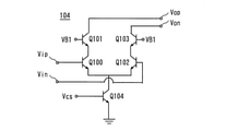
- FIG. 5 is a circuit diagram showing the configuration of the output circuit 104.
- the output circuit 104 is composed of transistors Q100 to Q104.
- Driver circuits generally operate on multiple supply voltages to reduce power consumption. For example, as shown in FIG. 4, the power supply voltage VCS of the driver circuit 100 and the power supply voltage VDC of the MZM200 may be separately configured (see Non-Patent Document 1).
- the power supply voltage VDC of the MZM200 is applied to the output signal terminal Voutp of the driver circuit 100 (non-inverting output terminal Vop of the output circuit 104) via the resistor R200 and the electrode 201.
- a power supply voltage VDC is applied to the output signal terminal Voutn of the driver circuit 100 (inverted output terminal Von of the output circuit 104) via the resistor R201 and the electrode 202. In this way, the power supply voltage of the output circuit 104 is supplied from the MZM200 side.
- the common voltage of the input transistors Q100 and Q102 of the output circuit 104, the bias voltage VB1 applied to the base terminals of the output transistors Q101 and Q103, and the bias voltage Vcs applied to the base terminal of the current source transistor Q104 are the driver circuit 100. Generated from the power supply voltage VCS of.
- the input transistors Q100, Q102 and output transistors Q101, Q103 of the output circuit 104 have a withstand voltage or more. A voltage may be applied and the transistors Q100 to Q103 may be destroyed. Therefore, in the conventional technique, for example, when the power is turned on, the power supply voltages of both the driver circuit 100 and the MZM200 are gradually increased to a desired voltage so that the transistors Q100 to Q103 are not applied with a voltage higher than the withstand voltage. On the contrary, when the power supply was cut off, the power supply voltages of the driver circuit 100 and the MZM200 were gradually lowered.
- the present invention has been made to solve the above problems, and an object of the present invention is to provide a driver circuit capable of simplifying a power supply sequence as compared with the conventional case.
- the driver circuit of the present invention is an open collector type configured to drive an optical modulator connected to a first output signal terminal on the positive phase side and a second output signal terminal on the negative phase side of the driver circuit.
- the output circuit includes first and second transistors in which a differential signal for driving the optical modulator is input to the base terminal, and the base terminal is connected to a first bias voltage.
- the collector terminal is connected to the first output signal terminal, the emitter terminal is connected to the collector terminal of the first transistor, and the base terminal is connected to the first bias voltage.
- the terminal is connected to the second output signal terminal, the emitter terminal is connected to the collector terminal of the second transistor, and the collector terminal is connected to the emitter terminal of the first and second transistors.
- the fifth transistor is configured so that the emitter terminal is connected to the ground and a current corresponding to the second bias voltage applied to the base terminal is passed through the first, second, third, and fourth transistors. It is configured to control the current flowing through the first, second, third, and fourth transistors according to the common voltage between the transistor and the first output signal terminal and the second output signal terminal. It is characterized by being composed of a withstand voltage protection circuit.
- a breakdown voltage protection circuit that controls the current flowing through the first, second, third, and fourth transistors according to the common voltage between the first output signal terminal and the second output signal terminal is output.
- the power supply sequence of the driver circuit and the optical modulator can be simplified as compared with the conventional case.
- the present invention since a complicated power supply control circuit or program is not required, it is possible to realize the withstand voltage protection of the transistor of the output circuit with a small area and low cost.
- FIG. 1 is a circuit diagram showing a configuration of an output circuit of a driver circuit according to a first embodiment of the present invention.
- FIG. 2 is a circuit diagram showing a configuration of an output circuit of a driver circuit according to a second embodiment of the present invention.
- FIG. 3 is a circuit diagram showing a configuration of an output circuit of the driver circuit according to the third embodiment of the present invention.
- FIG. 4 is a circuit diagram showing the configuration of a conventional driver circuit.
- FIG. 5 is a circuit diagram showing a configuration of an output circuit of a conventional driver circuit.
- FIG. 1 is a circuit diagram showing a configuration of an output circuit of a driver circuit according to a first embodiment of the present invention.
- the output circuit 104a is used instead of the output circuit 104. Therefore, the driver circuit 100 and the MZM200 will be described with reference to the reference numerals in FIG.
- the base terminal is connected to the input transistor Q100 connected to the non-inverting input terminal Vip of the output circuit 104a, the base terminal is connected to the bias voltage VB1, and the collector terminal is the non-inverting output terminal Vop (driver) of the output circuit 104a.
- the output transistor Q101 is connected to the output signal terminal Voutp on the positive phase side of the circuit 100, the emitter terminal is connected to the collector terminal of the input transistor Q100, and the base terminal is connected to the inverting input terminal Vin of the output circuit 104a.
- the transistor Q102 and the base terminal are connected to the bias voltage VB1, the collector terminal is connected to the inverting output terminal Von (output signal terminal Voutn on the opposite phase side of the driver circuit 100) of the output circuit 104a, and the emitter terminal is the input transistor Q102.
- the output transistor Q103 connected to the collector terminal, the current source transistor Q104 in which the collector terminal is connected to the emitter terminals of the input transistors Q100 and Q102 and the emitter terminal is connected to the ground, and the output signal terminal Voutp and the output signal terminal Voutn.
- the resistors R102 and R103 connected in series between the two, one end connected to the connection point of the resistors R102 and R103, and one end connected to the other end of the resistor R104 and the other end connected to the ground. It is composed of a resistor R105, a gate terminal connected to a connection point of resistors R104 and R105, a drain terminal connected to a bias voltage Vcs, and a source terminal connected to a base terminal of a current source transistor Q104. ..
- the NOTE transistor Q105 constitutes a switch SW1 connected between the bias voltage Vcs and the base terminal of the current source transistor Q104.
- the switch SW1 is turned off when the connection points of the resistors R102 and R103 are floating or a ground voltage, and is turned on when the connection points of the resistors R102 and R103 are higher than the ground voltage.
- the resistors R102 to R105 and the switch SW1 form a withstand voltage protection circuit 300.
- the power supply voltage VCS of the driver circuit 100, the power supply voltage VDC of the MZM200, and the bias voltages VB1 and Vcs are positive voltages.
- a switch SW1 for turning on / off the application of the bias voltage Vcs to the base terminal of the current source transistor Q104 is provided, and the differential output signal terminals Voutp, Voutn of the driver circuit 100 (output terminal Vop of the output circuit 104a, The switch SW1 is controlled according to the common voltage of Von).
- the control signal applied to the control terminal of the switch SW1 resists the common voltage detected by the resistors R102 and R103 inserted between the output signal terminal Voutp and the output signal terminal Voutn. It is divided by R104 and R105 and shifted to the low voltage side.
- the reason why the common voltage is shifted to the low voltage side by resistance division is that the withstand voltage of the MIMO transistor Q105 used as the switch SW1 is lower than the withstand voltage of the bipolar transistors Q100 to Q104.
- the connection points of the resistors R102 and R103 may be directly connected to the control terminal of the switch SW1 without providing the resistors R104 and R105.
- the pressure resistance protection of this embodiment functions as follows. For example, when only the power supply of the driver circuit 100 is on and the power supply of the MZM200 is off, the differential output signal terminals Voutp and Voutn of the driver circuit 100 are floating or ground voltage. In this state, the control signal applied to the gate terminal of the nanotube transistor Q105 becomes Low, so that the Now's transistor Q105 is turned off. Therefore, the bias voltage Vcs is not supplied to the current source transistors Q104, and no current flows through the transistors Q100 to Q103 of the output circuit 104a, so that the transistors Q100 to Q103 do not receive a voltage higher than the withstand voltage.
- the common voltage of the differential output signal terminals Voutp and Voutn of the driver circuit 100 rises, and the control signal applied to the gate terminal of the MIMO transistor Q105. Is High, and the nanotube transistor Q105 is turned on. In this state, the bias voltage Vcs is supplied to the current source transistors Q104, and the current in normal operation flows through the transistors Q100 to Q103 of the output circuit 104a. Therefore, a voltage higher than the withstand voltage is not applied to the transistors Q100 to Q103.
- the power supply sequence can be simplified as compared with the conventional case. For example, the operation of simply turning on the power of the driver circuit 100 and then turning on the power of the MZM200 may be performed. When the power is cut off, the power of the MZM 200 may be turned off and then the power of the driver circuit 100 may be turned off. Further, in this embodiment, since a complicated power supply control circuit or program is not required, withstand voltage protection can be realized in a small area and at low cost.
- FIG. 2 is a circuit diagram showing a configuration of an output circuit of the driver circuit according to the second embodiment of the present invention.
- the output circuit 104b is used instead of the output circuit 104. Therefore, the driver circuit 100 and the MZM200 will be described with reference to the reference numerals in FIG.
- the output circuit 104b includes transistors Q100 to Q103, a current source transistor Q104 in which the base terminal is connected to the bias voltage Vcs, the collector terminal is connected to the emitter terminals of the input transistors Q100 and Q102, and the emitter terminal is connected to the ground.
- the resistors R102 and R103 and the gate terminal are connected to the connection points of the resistors R102 and R103, the drain terminal is connected to the collector terminal of the output transistor Q101 (the output signal terminal Voutp on the positive phase side of the driver circuit 100), and the source terminal is
- the polyclonal transistor Q106 connected to the power supply voltage VCS and the gate terminal are connected to the connection points of the resistors R102 and R103, and the drain terminal is connected to the collector terminal (output signal terminal Voutn on the opposite phase side of the driver circuit 100) of the output transistor Q103.
- It is composed of a polyclonal transistor Q107 which is connected and whose source terminal is connected to the power supply voltage VCS, and a resistor R106 whose one end is connected to the connection points of the resistors R102 and R103 and the other end is connected to the ground.
- the polyclonal transistor Q106 constitutes a switch SW2 connected between the power supply voltage VCS and the output signal terminal Voutp.
- the polyclonal transistor Q107 constitutes a switch SW3 connected between the power supply voltage VCS and the output signal terminal Voutn.
- the switches SW2 and SW3 are turned on when the connection points of the resistors R102 and R103 are floating or the ground voltage, and are turned off when the connection points of the resistors R102 and R103 are higher than the ground voltage.
- the resistors R102, R103, R106 and the switches SW2 and SW3 form a withstand voltage protection circuit 300a.
- switches SW2 and SW3 for turning on / off the application of the power supply voltage VCS to the collector terminals of the output transistors Q101 and Q103 are provided, and the differential output signal terminals Voutp and Voutn of the driver circuit 100 (output of the output circuit 104b) are provided.
- the switches SW2 and SW3 are controlled according to the common voltage of the terminals Vop and Von).
- the pressure resistance protection of this embodiment functions as follows. For example, when only the power supply of the driver circuit 100 is on and the power supply of the MZM200 is off, the differential output signal terminals Voutp and Voutn of the driver circuit 100 are floating or ground voltage. In this state, the control signal applied to the gate terminals of the polyclonal transistors Q106 and Q107 becomes Low, so that the polyclonal transistors Q106 and Q107 are turned on. At this time, the power supply voltage VCS is supplied to the collector terminals of the output transistors Q101 and Q103, and the current flows through the transistors Q100 to Q103 of the output circuit 104b, so that the transistors Q100 to Q103 are not overvoltage.
- the common voltage of the differential output signal terminals Voutp and Voutn of the driver circuit 100 rises and is applied to the gate terminals of the polyclonal transistors Q106 and Q107.
- the control signal becomes High, and the polyclonal transistors Q106 and Q107 are turned off. In this state, the collector terminals of the output transistors Q101 and Q103 and the power supply voltage VCS are disconnected, and the collector terminals of the output transistors Q101 and Q103 return to the open state.
- the power supply voltage of the output circuit 104b is supplied from the MZM200 side and the current in normal operation flows through the transistors Q100 to Q103 of the output circuit 104b, the voltage exceeding the withstand voltage is not applied to the transistors Q100 to Q103.
- the power supply sequence can be simplified as compared with the conventional case. For example, the operation of simply turning on the power of the driver circuit 100 and then turning on the power of the MZM200 may be performed. When the power is cut off, the power of the MZM 200 may be turned off and then the power of the driver circuit 100 may be turned off. Further, in this embodiment, since a complicated power supply control circuit or program is not required, withstand voltage protection can be realized in a small area and at low cost.
- FIG. 3 is a circuit diagram showing a configuration of an output circuit of the driver circuit according to the third embodiment of the present invention.
- the output circuit 104c is used instead of the output circuit 104. Therefore, the driver circuit 100 and the MZM200 will be described with reference to the reference numerals in FIG.
- the output circuit 104c of the present embodiment has resistors R107 and R108 inserted between the drain terminals of the polyclonal transistors Q106 and Q107 and the collector terminals of the output transistors Q101 and Q103 in the output circuit 104b of the second embodiment. be.
- the resistors R102, R103, R106 to R108 and the switches SW2, SW3 (Prylmonistor Q106, Q107) form a withstand voltage protection circuit 300b.
- the power supply voltage VCS is applied to the collector terminals of the output transistors Q101 and Q103.
- the resistors R107 and R108 are present between the drain terminals of the polyclonal transistors Q106 and Q107 and the differential output signal terminals Voutp and Voutn of the driver circuit 100 (collector terminals of the output transistors Q101 and Q103). Since the influence of the parasitic capacitance of the polyclonal transistors Q106 and Q107 added to the differential output signal terminals Voutp and Voutn is weaker than that in the second embodiment, it is possible to widen the band of the driver circuit 100 during normal operation. Become.
- withstand voltage protection circuit that detects the common voltage of the output circuits 104a to 104c and automatically controls the current of the output circuits 104a to 104c according to the detected common voltage as in the first to third embodiments.
- the configuration of the withstand voltage protection circuit of the present invention is not limited to the first to third embodiments.
- the present invention can be applied to a driver circuit for driving an optical modulator.
Landscapes
- Physics & Mathematics (AREA)
- Nonlinear Science (AREA)
- General Physics & Mathematics (AREA)
- Optics & Photonics (AREA)
- Amplifiers (AREA)
- Optical Modulation, Optical Deflection, Nonlinear Optics, Optical Demodulation, Optical Logic Elements (AREA)
- Electronic Switches (AREA)
Abstract
Description
ドライバ回路は、一般的に消費電力を削減するために、複数の電源電圧で動作する。例えば、図4のようにドライバ回路100の電源電圧VCCとMZM200の電源電圧VDRとを分けた構成をとることがある(非特許文献1参照)。
以下、本発明の実施例について図面を参照して説明する。図1は本発明の第1の実施例に係るドライバ回路の出力回路の構成を示す回路図である。本実施例は、図4に示したドライバ回路100において、出力回路104の代わりに出力回路104aを用いるものなので、ドライバ回路100とMZM200については図4の符号を用いて説明する。
本実施例では、電流源トランジスタQ104のベース端子へのバイアス電圧Vcsの印加をオン/オフするスイッチSW1を設け、ドライバ回路100の差動出力信号端子Voutp,Voutn(出力回路104aの出力端子Vop,Von)のコモン電圧に応じてスイッチSW1の制御を行う。
次に、本発明の第2の実施例について説明する。図2は本発明の第2の実施例に係るドライバ回路の出力回路の構成を示す回路図である。本実施例は、図4に示したドライバ回路100において、出力回路104の代わりに出力回路104bを用いるものなので、ドライバ回路100とMZM200については図4の符号を用いて説明する。
次に、本発明の第3の実施例について説明する。図3は本発明の第3の実施例に係るドライバ回路の出力回路の構成を示す回路図である。本実施例は、図4に示したドライバ回路100において、出力回路104の代わりに出力回路104cを用いるものなので、ドライバ回路100とMZM200については図4の符号を用いて説明する。
抵抗R102,R103,R106~R108とスイッチSW2,SW3(PMOSトランジスタQ106,Q107)とは、耐圧保護回路300bを構成している。
Claims (6)
- ドライバ回路の正相側の第1の出力信号端子と逆相側の第2の出力信号端子とに接続された光変調器を駆動するように構成されたオープンコレクタ型の出力回路を備え、
前記出力回路は、
ベース端子に前記光変調器の駆動のための差動信号が入力される第1、第2のトランジスタと、
ベース端子が第1のバイアス電圧に接続され、コレクタ端子が前記第1の出力信号端子に接続され、エミッタ端子が前記第1のトランジスタのコレクタ端子に接続された第3のトランジスタと、
ベース端子が前記第1のバイアス電圧に接続され、コレクタ端子が前記第2の出力信号端子に接続され、エミッタ端子が前記第2のトランジスタのコレクタ端子に接続された第4のトランジスタと、
コレクタ端子が前記第1、第2のトランジスタのエミッタ端子に接続され、エミッタ端子がグラウンドに接続され、ベース端子に印加される第2のバイアス電圧に応じた電流を前記第1、第2、第3、第4のトランジスタに流すように構成された第5のトランジスタと、
前記第1の出力信号端子と前記第2の出力信号端子とのコモン電圧に応じて前記第1、第2、第3、第4のトランジスタに流れる電流を制御するように構成された耐圧保護回路とから構成されることを特徴とするドライバ回路。 - 請求項1記載のドライバ回路において、
前記耐圧保護回路は、
前記第1の出力信号端子と前記第2の出力信号端子との間に直列に接続された第1、第2の抵抗と、
前記第2のバイアス電圧と前記第5のトランジスタのベース端子との間に接続されたスイッチとから構成され、
前記スイッチは、前記第1、第2の抵抗の接続点がフローティングまたはグラウンド電圧のときにオフ状態となり、前記第1、第2の抵抗の接続点がグラウンド電圧よりも高い電圧のときにオン状態となることを特徴とするドライバ回路。 - 請求項2記載のドライバ回路において、
前記耐圧保護回路は、
一端が前記第1、第2の抵抗の接続点に接続された第3の抵抗と、
一端が前記第3の抵抗の他端に接続され、他端がグラウンドに接続された第4の抵抗とをさらに備え、
前記スイッチは、ゲート端子が前記第3、第4の抵抗の接続点に接続され、ドレイン端子が前記第2のバイアス電圧に接続され、ソース端子が前記第5のトランジスタのベース端子に接続されたNMOSトランジスタからなることを特徴とするドライバ回路。 - 請求項1記載のドライバ回路において、
前記耐圧保護回路は、
前記第1の出力信号端子と前記第2の出力信号端子との間に直列に接続された第1、第2の抵抗と、
ドライバ回路の電源電圧と前記第1の出力信号端子との間に接続された第1のスイッチと、
前記電源電圧と前記第2の出力信号端子との間に接続された第2のスイッチとから構成され、
前記第1、第2のスイッチは、前記第1、第2の抵抗の接続点がフローティングまたはグラウンド電圧のときにオン状態となり、前記第1、第2の抵抗の接続点がグラウンド電圧よりも高い電圧のときにオフ状態となることを特徴とするドライバ回路。 - 請求項4記載のドライバ回路において、
前記耐圧保護回路は、
一端が前記第1、第2の抵抗の接続点に接続され、他端がグラウンドに接続された第3の抵抗をさらに備え、
前記第1のスイッチは、ゲート端子が前記第1、第2の抵抗の接続点に接続され、ドレイン端子が前記第1の出力信号端子に接続され、ソース端子が前記電源電圧に接続された第1のPMOSトランジスタからなり、
前記第2のスイッチは、ゲート端子が前記第1、第2の抵抗の接続点に接続され、ドレイン端子が前記第2の出力信号端子に接続され、ソース端子が前記電源電圧に接続された第2のPMOSトランジスタからなることを特徴とするドライバ回路。 - 請求項4または5記載のドライバ回路において、
前記耐圧保護回路は、
前記第1のスイッチと前記第1の出力信号端子との間に接続された第4の抵抗と、
前記第2のスイッチと前記第2の出力信号端子との間に接続された第5の抵抗とをさらに備えることを特徴とするドライバ回路。
Priority Applications (3)
| Application Number | Priority Date | Filing Date | Title |
|---|---|---|---|
| JP2022538528A JP7371786B2 (ja) | 2020-07-21 | 2020-07-21 | ドライバ回路 |
| US18/006,124 US12345965B2 (en) | 2020-07-21 | 2020-07-21 | Driver circuit |
| PCT/JP2020/028256 WO2022018825A1 (ja) | 2020-07-21 | 2020-07-21 | ドライバ回路 |
Applications Claiming Priority (1)
| Application Number | Priority Date | Filing Date | Title |
|---|---|---|---|
| PCT/JP2020/028256 WO2022018825A1 (ja) | 2020-07-21 | 2020-07-21 | ドライバ回路 |
Publications (1)
| Publication Number | Publication Date |
|---|---|
| WO2022018825A1 true WO2022018825A1 (ja) | 2022-01-27 |
Family
ID=79729120
Family Applications (1)
| Application Number | Title | Priority Date | Filing Date |
|---|---|---|---|
| PCT/JP2020/028256 Ceased WO2022018825A1 (ja) | 2020-07-21 | 2020-07-21 | ドライバ回路 |
Country Status (3)
| Country | Link |
|---|---|
| US (1) | US12345965B2 (ja) |
| JP (1) | JP7371786B2 (ja) |
| WO (1) | WO2022018825A1 (ja) |
Cited By (1)
| Publication number | Priority date | Publication date | Assignee | Title |
|---|---|---|---|---|
| WO2025191838A1 (ja) * | 2024-03-15 | 2025-09-18 | Ntt株式会社 | ドライバ回路 |
Citations (6)
| Publication number | Priority date | Publication date | Assignee | Title |
|---|---|---|---|---|
| US20090245813A1 (en) * | 2008-03-31 | 2009-10-01 | Kitel Technologies Llc | Modulator driver with multi-channel active alignment |
| JP2014050087A (ja) * | 2012-09-04 | 2014-03-17 | Renesas Electronics Corp | 差動出力回路および半導体装置 |
| JP2014160176A (ja) * | 2013-02-20 | 2014-09-04 | Sumitomo Electric Ind Ltd | 駆動回路 |
| WO2016185716A1 (ja) * | 2015-05-20 | 2016-11-24 | パナソニックIpマネジメント株式会社 | 差動出力回路 |
| US20200064707A1 (en) * | 2018-08-24 | 2020-02-27 | Ciena Corporation | Optical modulator and optical modulator driver devices and methods utilizing independent arm bias to mitigate fabrication errors |
| JP2020072321A (ja) * | 2018-10-30 | 2020-05-07 | 日本電信電話株式会社 | 線形増幅器 |
Family Cites Families (3)
| Publication number | Priority date | Publication date | Assignee | Title |
|---|---|---|---|---|
| US6005438A (en) * | 1997-12-10 | 1999-12-21 | National Semiconductor Corporation | Output high voltage clamped circuit for low voltage differential swing applications in the case of overload |
| US6590422B1 (en) * | 2002-03-27 | 2003-07-08 | Analog Devices, Inc. | Low voltage differential signaling (LVDS) drivers and systems |
| JP2016054452A (ja) * | 2014-09-04 | 2016-04-14 | 住友電気工業株式会社 | 光変調器駆動回路 |
-
2020
- 2020-07-21 US US18/006,124 patent/US12345965B2/en active Active
- 2020-07-21 JP JP2022538528A patent/JP7371786B2/ja active Active
- 2020-07-21 WO PCT/JP2020/028256 patent/WO2022018825A1/ja not_active Ceased
Patent Citations (6)
| Publication number | Priority date | Publication date | Assignee | Title |
|---|---|---|---|---|
| US20090245813A1 (en) * | 2008-03-31 | 2009-10-01 | Kitel Technologies Llc | Modulator driver with multi-channel active alignment |
| JP2014050087A (ja) * | 2012-09-04 | 2014-03-17 | Renesas Electronics Corp | 差動出力回路および半導体装置 |
| JP2014160176A (ja) * | 2013-02-20 | 2014-09-04 | Sumitomo Electric Ind Ltd | 駆動回路 |
| WO2016185716A1 (ja) * | 2015-05-20 | 2016-11-24 | パナソニックIpマネジメント株式会社 | 差動出力回路 |
| US20200064707A1 (en) * | 2018-08-24 | 2020-02-27 | Ciena Corporation | Optical modulator and optical modulator driver devices and methods utilizing independent arm bias to mitigate fabrication errors |
| JP2020072321A (ja) * | 2018-10-30 | 2020-05-07 | 日本電信電話株式会社 | 線形増幅器 |
Non-Patent Citations (1)
| Title |
|---|
| WAKITA, H. ET AL.: "Recent Advance in Ultra-High Bandwidth Coherent Driver Modulator", PROCEEDINGS OF SPIE, vol. 10947, no. 109470L, 1 February 2019 (2019-02-01), XP060120314, DOI: 10.1117/12.2511119 * |
Cited By (1)
| Publication number | Priority date | Publication date | Assignee | Title |
|---|---|---|---|---|
| WO2025191838A1 (ja) * | 2024-03-15 | 2025-09-18 | Ntt株式会社 | ドライバ回路 |
Also Published As
| Publication number | Publication date |
|---|---|
| US12345965B2 (en) | 2025-07-01 |
| US20230288735A1 (en) | 2023-09-14 |
| JP7371786B2 (ja) | 2023-10-31 |
| JPWO2022018825A1 (ja) | 2022-01-27 |
Similar Documents
| Publication | Publication Date | Title |
|---|---|---|
| US8054123B2 (en) | Fast differential level shifter and boot strap driver including the same | |
| US20180145644A1 (en) | Transimpedance amplifier with variable inductance input reducing peak variation over gain | |
| JP6520638B2 (ja) | 駆動回路及び可変利得増幅器 | |
| US6081133A (en) | Universal receiver device | |
| US4431972A (en) | Push-pull amplifier | |
| JP7371786B2 (ja) | ドライバ回路 | |
| US10367458B2 (en) | Signal amplifier | |
| US10564450B1 (en) | Electrical amplifier and electro-optical device comprising an electrical amplifier | |
| GB2295287A (en) | Wideband constant impedance amplifiers | |
| JP6359928B2 (ja) | ドライバ回路 | |
| US10423016B2 (en) | Driver for optical modulator | |
| JP2005217194A (ja) | レーザダイオードの駆動回路 | |
| CN117356031A (zh) | 放大电路和电子设备 | |
| JP5666415B2 (ja) | 電界吸収型光変調器の駆動回路 | |
| WO2022018824A1 (ja) | 増幅回路およびドライバ回路 | |
| JP2005210558A (ja) | 光電流・電圧変換回路 | |
| US8164385B2 (en) | Amplifier circuit | |
| JPH05152662A (ja) | 半導体発光素子駆動回路 | |
| US7592794B2 (en) | Integrated low power received signal strength indicator (RSSI) with linear characteristic | |
| JP4036506B2 (ja) | 差動増幅器 | |
| US6870389B2 (en) | Differential circuit with current overshoot suppression | |
| JPS63285990A (ja) | レ−ザダイオ−ド駆動回路 | |
| JPS6110340Y2 (ja) | ||
| KR100265347B1 (ko) | 입력 버퍼링 장치 | |
| JP2021111885A (ja) | 差動増幅回路 |
Legal Events
| Date | Code | Title | Description |
|---|---|---|---|
| 121 | Ep: the epo has been informed by wipo that ep was designated in this application |
Ref document number: 20945947 Country of ref document: EP Kind code of ref document: A1 |
|
| ENP | Entry into the national phase |
Ref document number: 2022538528 Country of ref document: JP Kind code of ref document: A |
|
| NENP | Non-entry into the national phase |
Ref country code: DE |
|
| 122 | Ep: pct application non-entry in european phase |
Ref document number: 20945947 Country of ref document: EP Kind code of ref document: A1 |
|
| WWG | Wipo information: grant in national office |
Ref document number: 18006124 Country of ref document: US |