WO2022018817A1 - 半導体装置 - Google Patents
半導体装置 Download PDFInfo
- Publication number
- WO2022018817A1 WO2022018817A1 PCT/JP2020/028186 JP2020028186W WO2022018817A1 WO 2022018817 A1 WO2022018817 A1 WO 2022018817A1 JP 2020028186 W JP2020028186 W JP 2020028186W WO 2022018817 A1 WO2022018817 A1 WO 2022018817A1
- Authority
- WO
- WIPO (PCT)
- Prior art keywords
- semiconductor device
- package module
- cooler
- resin package
- semiconductor
- Prior art date
- Legal status (The legal status is an assumption and is not a legal conclusion. Google has not performed a legal analysis and makes no representation as to the accuracy of the status listed.)
- Ceased
Links
Images



















Classifications
-
- H—ELECTRICITY
- H10—SEMICONDUCTOR DEVICES; ELECTRIC SOLID-STATE DEVICES NOT OTHERWISE PROVIDED FOR
- H10W—GENERIC PACKAGES, INTERCONNECTIONS, CONNECTORS OR OTHER CONSTRUCTIONAL DETAILS OF DEVICES COVERED BY CLASS H10
- H10W40/00—Arrangements for thermal protection or thermal control
- H10W40/40—Arrangements for thermal protection or thermal control involving heat exchange by flowing fluids
- H10W40/47—Arrangements for thermal protection or thermal control involving heat exchange by flowing fluids by flowing liquids, e.g. forced water cooling
-
- H—ELECTRICITY
- H10—SEMICONDUCTOR DEVICES; ELECTRIC SOLID-STATE DEVICES NOT OTHERWISE PROVIDED FOR
- H10W—GENERIC PACKAGES, INTERCONNECTIONS, CONNECTORS OR OTHER CONSTRUCTIONAL DETAILS OF DEVICES COVERED BY CLASS H10
- H10W40/00—Arrangements for thermal protection or thermal control
- H10W40/20—Arrangements for cooling
- H10W40/25—Arrangements for cooling characterised by their materials
- H10W40/255—Arrangements for cooling characterised by their materials having a laminate or multilayered structure, e.g. direct bond copper [DBC] ceramic substrates
-
- H—ELECTRICITY
- H10—SEMICONDUCTOR DEVICES; ELECTRIC SOLID-STATE DEVICES NOT OTHERWISE PROVIDED FOR
- H10W—GENERIC PACKAGES, INTERCONNECTIONS, CONNECTORS OR OTHER CONSTRUCTIONAL DETAILS OF DEVICES COVERED BY CLASS H10
- H10W70/00—Package substrates; Interposers; Redistribution layers [RDL]
- H10W70/40—Leadframes
- H10W70/421—Shapes or dispositions
-
- H—ELECTRICITY
- H10—SEMICONDUCTOR DEVICES; ELECTRIC SOLID-STATE DEVICES NOT OTHERWISE PROVIDED FOR
- H10W—GENERIC PACKAGES, INTERCONNECTIONS, CONNECTORS OR OTHER CONSTRUCTIONAL DETAILS OF DEVICES COVERED BY CLASS H10
- H10W70/00—Package substrates; Interposers; Redistribution layers [RDL]
- H10W70/40—Leadframes
- H10W70/481—Leadframes for devices being provided for in groups H10D8/00 - H10D48/00
-
- H—ELECTRICITY
- H10—SEMICONDUCTOR DEVICES; ELECTRIC SOLID-STATE DEVICES NOT OTHERWISE PROVIDED FOR
- H10W—GENERIC PACKAGES, INTERCONNECTIONS, CONNECTORS OR OTHER CONSTRUCTIONAL DETAILS OF DEVICES COVERED BY CLASS H10
- H10W74/00—Encapsulations, e.g. protective coatings
- H10W74/10—Encapsulations, e.g. protective coatings characterised by their shape or disposition
- H10W74/111—Encapsulations, e.g. protective coatings characterised by their shape or disposition the semiconductor body being completely enclosed
- H10W74/114—Encapsulations, e.g. protective coatings characterised by their shape or disposition the semiconductor body being completely enclosed by a substrate and the encapsulations
-
- H—ELECTRICITY
- H10—SEMICONDUCTOR DEVICES; ELECTRIC SOLID-STATE DEVICES NOT OTHERWISE PROVIDED FOR
- H10W—GENERIC PACKAGES, INTERCONNECTIONS, CONNECTORS OR OTHER CONSTRUCTIONAL DETAILS OF DEVICES COVERED BY CLASS H10
- H10W72/00—Interconnections or connectors in packages
- H10W72/071—Connecting or disconnecting
- H10W72/073—Connecting or disconnecting of die-attach connectors
- H10W72/07351—Connecting or disconnecting of die-attach connectors characterised by changes in properties of the die-attach connectors during connecting
- H10W72/07354—Connecting or disconnecting of die-attach connectors characterised by changes in properties of the die-attach connectors during connecting changes in dispositions
-
- H—ELECTRICITY
- H10—SEMICONDUCTOR DEVICES; ELECTRIC SOLID-STATE DEVICES NOT OTHERWISE PROVIDED FOR
- H10W—GENERIC PACKAGES, INTERCONNECTIONS, CONNECTORS OR OTHER CONSTRUCTIONAL DETAILS OF DEVICES COVERED BY CLASS H10
- H10W72/00—Interconnections or connectors in packages
- H10W72/071—Connecting or disconnecting
- H10W72/075—Connecting or disconnecting of bond wires
-
- H—ELECTRICITY
- H10—SEMICONDUCTOR DEVICES; ELECTRIC SOLID-STATE DEVICES NOT OTHERWISE PROVIDED FOR
- H10W—GENERIC PACKAGES, INTERCONNECTIONS, CONNECTORS OR OTHER CONSTRUCTIONAL DETAILS OF DEVICES COVERED BY CLASS H10
- H10W72/00—Interconnections or connectors in packages
- H10W72/30—Die-attach connectors
- H10W72/341—Dispositions of die-attach connectors, e.g. layouts
- H10W72/347—Dispositions of multiple die-attach connectors
-
- H—ELECTRICITY
- H10—SEMICONDUCTOR DEVICES; ELECTRIC SOLID-STATE DEVICES NOT OTHERWISE PROVIDED FOR
- H10W—GENERIC PACKAGES, INTERCONNECTIONS, CONNECTORS OR OTHER CONSTRUCTIONAL DETAILS OF DEVICES COVERED BY CLASS H10
- H10W72/00—Interconnections or connectors in packages
- H10W72/50—Bond wires
- H10W72/551—Materials of bond wires
- H10W72/552—Materials of bond wires comprising metals or metalloids, e.g. silver
- H10W72/5524—Materials of bond wires comprising metals or metalloids, e.g. silver comprising aluminium [Al]
-
- H—ELECTRICITY
- H10—SEMICONDUCTOR DEVICES; ELECTRIC SOLID-STATE DEVICES NOT OTHERWISE PROVIDED FOR
- H10W—GENERIC PACKAGES, INTERCONNECTIONS, CONNECTORS OR OTHER CONSTRUCTIONAL DETAILS OF DEVICES COVERED BY CLASS H10
- H10W72/00—Interconnections or connectors in packages
- H10W72/851—Dispositions of multiple connectors or interconnections
-
- H—ELECTRICITY
- H10—SEMICONDUCTOR DEVICES; ELECTRIC SOLID-STATE DEVICES NOT OTHERWISE PROVIDED FOR
- H10W—GENERIC PACKAGES, INTERCONNECTIONS, CONNECTORS OR OTHER CONSTRUCTIONAL DETAILS OF DEVICES COVERED BY CLASS H10
- H10W72/00—Interconnections or connectors in packages
- H10W72/851—Dispositions of multiple connectors or interconnections
- H10W72/853—On the same surface
- H10W72/865—Die-attach connectors and bond wires
-
- H—ELECTRICITY
- H10—SEMICONDUCTOR DEVICES; ELECTRIC SOLID-STATE DEVICES NOT OTHERWISE PROVIDED FOR
- H10W—GENERIC PACKAGES, INTERCONNECTIONS, CONNECTORS OR OTHER CONSTRUCTIONAL DETAILS OF DEVICES COVERED BY CLASS H10
- H10W72/00—Interconnections or connectors in packages
- H10W72/851—Dispositions of multiple connectors or interconnections
- H10W72/874—On different surfaces
- H10W72/884—Die-attach connectors and bond wires
-
- H—ELECTRICITY
- H10—SEMICONDUCTOR DEVICES; ELECTRIC SOLID-STATE DEVICES NOT OTHERWISE PROVIDED FOR
- H10W—GENERIC PACKAGES, INTERCONNECTIONS, CONNECTORS OR OTHER CONSTRUCTIONAL DETAILS OF DEVICES COVERED BY CLASS H10
- H10W72/00—Interconnections or connectors in packages
- H10W72/90—Bond pads, in general
- H10W72/951—Materials of bond pads
- H10W72/952—Materials of bond pads comprising metals or metalloids, e.g. PbSn, Ag or Cu
-
- H—ELECTRICITY
- H10—SEMICONDUCTOR DEVICES; ELECTRIC SOLID-STATE DEVICES NOT OTHERWISE PROVIDED FOR
- H10W—GENERIC PACKAGES, INTERCONNECTIONS, CONNECTORS OR OTHER CONSTRUCTIONAL DETAILS OF DEVICES COVERED BY CLASS H10
- H10W74/00—Encapsulations, e.g. protective coatings
- H10W74/10—Encapsulations, e.g. protective coatings characterised by their shape or disposition
- H10W74/111—Encapsulations, e.g. protective coatings characterised by their shape or disposition the semiconductor body being completely enclosed
-
- H—ELECTRICITY
- H10—SEMICONDUCTOR DEVICES; ELECTRIC SOLID-STATE DEVICES NOT OTHERWISE PROVIDED FOR
- H10W—GENERIC PACKAGES, INTERCONNECTIONS, CONNECTORS OR OTHER CONSTRUCTIONAL DETAILS OF DEVICES COVERED BY CLASS H10
- H10W90/00—Package configurations
- H10W90/701—Package configurations characterised by the relative positions of pads or connectors relative to package parts
- H10W90/731—Package configurations characterised by the relative positions of pads or connectors relative to package parts of die-attach connectors
- H10W90/736—Package configurations characterised by the relative positions of pads or connectors relative to package parts of die-attach connectors between a chip and a stacked lead frame, conducting package substrate or heat sink
-
- H—ELECTRICITY
- H10—SEMICONDUCTOR DEVICES; ELECTRIC SOLID-STATE DEVICES NOT OTHERWISE PROVIDED FOR
- H10W—GENERIC PACKAGES, INTERCONNECTIONS, CONNECTORS OR OTHER CONSTRUCTIONAL DETAILS OF DEVICES COVERED BY CLASS H10
- H10W90/00—Package configurations
- H10W90/701—Package configurations characterised by the relative positions of pads or connectors relative to package parts
- H10W90/751—Package configurations characterised by the relative positions of pads or connectors relative to package parts of bond wires
- H10W90/755—Package configurations characterised by the relative positions of pads or connectors relative to package parts of bond wires between a chip and a laterally-adjacent insulating package substrate, interpose or RDL
Definitions
- the technology disclosed in the specification of the present application relates to a semiconductor device.
- Patent Document 1 discloses a semiconductor device having a semiconductor module bonded to a cooler.
- the semiconductor module contacts the cooler through a metal block exposed from the lower surface of the mold resin, and dissipates the generated heat.
- the technique disclosed in the present specification has been made in view of the above-mentioned problems, and is a technique for effectively dissipating heat from the semiconductor device while keeping the height of the semiconductor device low. be.
- the semiconductor device includes a semiconductor module and a cooler for cooling the semiconductor module, and the semiconductor module is formed on a metal block and an upper surface of the metal block.
- a semiconductor element provided, a terminal connected to the semiconductor element, a part of the terminal, a metal block, and a resin covering the semiconductor element are provided, and the cooler is in contact with the lower surface of the semiconductor module.
- a metal base provided in a region including the semiconductor module in a plan view, and a cooling pipe arranged on the upper surface of the metal base and circulating a refrigerant for cooling the semiconductor module are provided, and the cooling pipe is provided.
- the semiconductor module is provided so as to surround at least a part thereof in a plan view.
- the cooling pipe of the cooler is arranged so as to surround the semiconductor module in a plan view, the height of the entire structure of the semiconductor device can be kept low. can.
- ordinal numbers such as “first” or “second” may be used in the description described below, these terms facilitate the understanding of the content of the embodiments. It is used for convenience, and is not limited to the order that can be generated by these ordinal numbers.
- the upper surface of " or “the lower surface of " in addition to the upper surface itself or the lower surface itself of the target component, the upper surface of the target component.
- it shall include a state in which other components are formed on the lower surface. That is, for example, when the description "B provided on the upper surface of the instep” is described, it does not prevent another component " ⁇ " from intervening between the instep and the second.
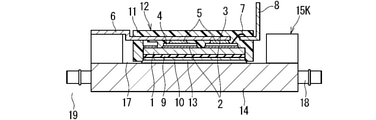
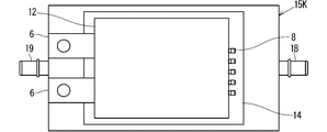
- FIG. 47 is a cross-sectional view schematically showing an example of the configuration of the semiconductor device according to the present embodiment. Further, FIG. 48 is a cross-sectional view from another direction schematically showing an example of the configuration of the semiconductor device according to the present embodiment. Further, FIG. 49 is a plan view schematically showing an example of the configuration of the semiconductor device according to the present embodiment.
- the semiconductor device includes a resin package module 12 and a cooler 15K that cools the resin package module 12 by water cooling.
- the resin package module 12 includes a metal block 1 made of copper or the like, a semiconductor element 3 containing silicon (Si) or the like bonded to the upper surface of the metal block 1 via a brazing material 2 such as solder, and the metal block 1.
- the main terminal 6 made of copper or the like, the signal terminal 8 made of copper or the like connected to the semiconductor element 3 via a wire bond 7 made of aluminum or the like, and the lower surface of the metal block 1 are provided.
- the main terminal 6 and the signal terminal 8 each project from the side surface of the mold resin 11.
- the cooler 15K made of aluminum or the like is arranged in contact with the lower surface of the resin package module 12, specifically, the lower surface of the metal plate 10 while being arranged at a position overlapping the resin package module 12 in a plan view. ..
- the cooler 15K includes a metal base 14 made of copper or the like that contacts the lower surface of the metal plate 10 via the thermal paste 13, and a cooling water introduction nipple 18 that introduces the cooling water 22 into the cooling pipe in the metal base 14.
- a cooling water drainage nipple 19 for discharging the cooling water 22 from the cooling pipe in the metal base 14 is provided.
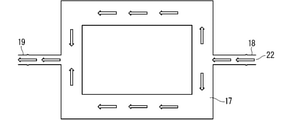
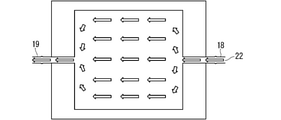
- FIG. 50 is a diagram schematically showing the circulation flow of the cooling water 22 in the cooler 15K.
- the cooler 15K circulates the cooling water 22 in the cooling pipe in the metal base 14. By doing so, the cooler 15K cools the resin package module 12 via the metal base 14.
- FIG. 1 is a cross-sectional view schematically showing an example of the configuration of a semiconductor device according to the present embodiment.
- FIG. 2 is a cross-sectional view from another direction schematically showing an example of the configuration of the semiconductor device according to the present embodiment.
- FIG. 3 is a plan view schematically showing an example of the configuration of the semiconductor device according to the present embodiment.
- the semiconductor device includes a resin package module 12 and a cooler 15 that cools the resin package module 12 by water cooling.
- the resin package module 12 includes a metal block 1 made of copper or the like, a semiconductor element 3 containing silicon (Si) or the like bonded to the upper surface of the metal block 1 via a brazing material 2 such as solder, and the metal block 1.
- the main terminal 6 made of copper or the like, the signal terminal 8 made of copper or the like connected to the semiconductor element 3 via a wire bond 7 made of aluminum or the like, and the lower surface of the metal block 1 are provided.
- the main terminal 6 and the signal terminal 8 each project from the side surface of the mold resin 11.
- the cooler 15 made of aluminum or the like surrounds the resin package module 12 in a plan view, and is arranged in contact with the lower surface of the resin package module 12, specifically, the lower surface of the metal plate 10.
- the cooler 15 is provided in a region larger than the region overlapping the resin package module 12 in a plan view, and has a metal base 16 formed of copper or the like that contacts the lower surface of the metal plate 10 via the thermal paste 13.
- the introduction nipple 18 and the cooling water draining nipple 19 for discharging the cooling water 22 from the cooling pipe 17 are provided.
- the cooler 15 in the present embodiment cools the resin package module 12 by water cooling of the cooling water 22 circulating in the cooling pipe 17, but other refrigerants such as air cooling of the gas circulating in the cooling pipe 17 are used.
- the resin package module 12 may be cooled by the method using the above. This also applies to the cooler in other embodiments.
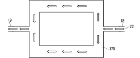
- FIG. 4 is a diagram schematically showing the circulation flow of the cooling water 22 in the cooler 15. As shown in FIG. 4, the cooler 15 circulates the cooling water 22 in the cooling pipe 17. By doing so, the cooler 15 cools the resin package module 12 via the metal base 16.
- the cooler 15 transfers heat generated from the semiconductor element 3 and heat generated from the semiconductor element 4 transmitted through the metal block 1, the insulating material 9, the metal plate 10, and the thermal paste 13 in the resin package module 12. Heat is dissipated by the cooling water 22 circulating in the cooling pipe 17 via the metal base 16.
- the semiconductor element 3 is, for example, an insulated gate type bipolar transistor (that is, an IGBT) or a metal-oxide-semisonic field effect transistor (that is, a MOSFET) or the like. Is. Further, the semiconductor element 4 is, for example, a diode or the like.
- the semiconductor used for the semiconductor element 3 and the semiconductor element 4 in addition to silicon (Si), for example, a wide bandgap semiconductor such as silicon carbide (SiC) is assumed.
- the wide bandgap semiconductor generally refers to a semiconductor having a forbidden band width of about 2 eV or more, a group 3 nitride such as gallium nitride (GaN), a group 2 oxide such as zinc oxide (ZnO), and selenium.
- Group 2 chalcogenides such as zinc oxide (ZnSe), diamonds, silicon carbide and the like are known. In this embodiment, the case where silicon carbide is used will be described, but other semiconductors and wide bandgap semiconductors can be similarly applied.
- the cooling pipe 17 of the cooler 15 is arranged so as to surround the resin package module 12 in a plan view, the height of the entire structure of the semiconductor device can be kept low.
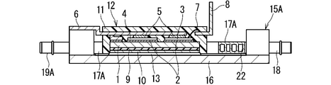
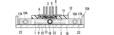
- FIG. 5 is a cross-sectional view schematically showing an example of the configuration of the semiconductor device according to the present embodiment.
- FIG. 6 is a cross-sectional view from another direction schematically showing an example of the configuration of the semiconductor device according to the present embodiment.
- FIG. 7 is a plan view schematically showing an example of the configuration of the semiconductor device according to the present embodiment.
- the semiconductor device includes a resin package module 12 and a cooler 15A that cools the resin package module 12 by water cooling.
- the cooler 15A made of aluminum or the like surrounds the resin package module 12 in a plan view and is arranged in contact with the lower surface of the resin package module 12, specifically, the lower surface of the metal plate 10.
- the cooler 15A is arranged on the upper surface of the metal base 16 and the metal base 16 formed of copper or the like that contacts the lower surface of the metal plate 10 via the thermal paste 13, and the resin package module 12 is partially formed in a plan view.
- Cooling pipe 17A made of aluminum or the like arranged so as to surround (that is, only a part of the side surface), cooling water introduction nipple 18 for introducing cooling water 22 into the cooling pipe 17A, and cooling from the cooling pipe 17A. It is provided with two cooling water drainage nipples 19A for discharging water 22.
- the cooling water introduction nipple 18 is provided on the straight portion of the cooling pipe 17A that partially surrounds the resin package module 12 in a plan view. Further, the two cooling water drainage nipples 19A are provided at both ends of the cooling pipe 17A that partially surrounds the resin package module 12 in a plan view.
- FIG. 8 is a diagram schematically showing the circulation flow of the cooling water 22 in the cooler 15A. As shown in FIG. 8, the cooler 15A circulates the cooling water 22 in the cooling pipe 17A. By doing so, the cooler 15A cools the resin package module 12 via the metal base 16.
- the cooler 15A receives heat generated from the semiconductor element 3 and heat generated from the semiconductor element 4 transmitted through the metal block 1, the insulating material 9, the metal plate 10, and the thermal paste 13 in the resin package module 12. Heat is dissipated by the cooling water 22 circulating in the cooling pipe 17A via the metal base 16.
- the cooling pipe 17A of the cooler 15A is arranged so as to partially surround the resin package module 12 in a plan view, the height of the entire structure of the semiconductor device can be kept low. Further, since the cooling pipe 17A is arranged so as not to surround the entire circumference of the resin package module 12 in a plan view, the occupied area (foot space) of the semiconductor device can be reduced.
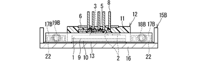
- FIG. 9 is a cross-sectional view schematically showing an example of the configuration of the semiconductor device according to the present embodiment.
- FIG. 10 is a cross-sectional view from another direction schematically showing an example of the configuration of the semiconductor device according to the present embodiment.
- FIG. 11 is a plan view schematically showing an example of the configuration of the semiconductor device according to the present embodiment.
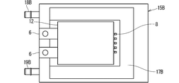
- the semiconductor device includes a resin package module 12 and a cooler 15B that cools the resin package module 12 by water cooling.
- the cooler 15B made of aluminum or the like surrounds the resin package module 12 in a plan view and is arranged in contact with the lower surface of the resin package module 12, specifically, the lower surface of the metal plate 10.
- the cooler 15B has a metal base 16 formed of copper or the like that contacts the lower surface of the metal plate 10 via the thermal paste 13, and is arranged on the upper surface of the metal base 16 and partially comprises the resin package module 12 in a plan view.
- the cooling water introduction nipple 18B is provided at one end in the longitudinal direction of the cooling pipe 17B that partially surrounds the resin package module 12 in a plan view. Further, the cooling water drainage nipple 19B is provided at the other end in the longitudinal direction of the cooling pipe 17B that partially surrounds the resin package module 12 in a plan view.
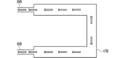
- FIG. 12 is a diagram schematically showing the circulation flow of the cooling water 22 in the cooler 15B. As shown in FIG. 12, the cooler 15B circulates the cooling water 22 in the cooling pipe 17B. By doing so, the cooler 15B cools the resin package module 12 via the metal base 16.
- the cooler 15B receives heat generated from the semiconductor element 3 and heat generated from the semiconductor element 4 transmitted through the metal block 1, the insulating material 9, the metal plate 10, and the thermal paste 13 in the resin package module 12. Heat is dissipated by the cooling water 22 circulating in the cooling pipe 17B via the metal base 16.
- the shape of the cooling pipe 17B shown in FIG. 12 can be applied to other embodiments.
- the cooling pipe 17B of the cooler 15B is arranged so as to partially surround the resin package module 12 in a plan view, the height of the entire structure of the semiconductor device can be kept low. Further, since the cooling pipe 17B is arranged so as not to surround the entire circumference of the resin package module 12 in a plan view, the occupied area (foot space) of the semiconductor device can be reduced. Further, since the nipple is not provided on the straight portion of the cooling pipe 17B, it is possible to suppress the manufacturing cost or improve the assembling property.
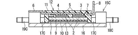
- FIG. 13 is a cross-sectional view schematically showing an example of the configuration of the semiconductor device according to the present embodiment.
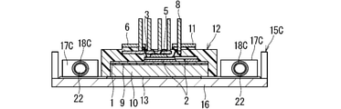
- FIG. 14 is a cross-sectional view from another direction schematically showing an example of the configuration of the semiconductor device according to the present embodiment.
- FIG. 15 is a plan view schematically showing an example of the configuration of the semiconductor device according to the present embodiment.
- the semiconductor device includes a resin package module 12 and a cooler 15C that cools the resin package module 12 by water cooling.
- the cooler 15C made of aluminum or the like surrounds the resin package module 12 in a plan view and is arranged in contact with the lower surface of the resin package module 12, specifically, the lower surface of the metal plate 10.
- the cooler 15C is a pair of a metal base 16 formed of copper or the like that comes into contact with the lower surface of the metal plate 10 via the thermal paste 13, and a pair of resin package modules 12 arranged on the upper surface of the metal base 16 and in a plan view.
- Cooling pipe 17C made of aluminum or the like arranged around the opposite side surfaces, cooling water introduction nipple 18C for introducing cooling water 22 into the cooling pipe 17C, and cooling water for discharging cooling water 22 from the cooling pipe 17C. It is equipped with a drainage nipple 19C.
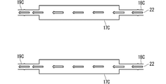
- the cooling pipe 17C is a linear pipe along the sides facing each other, and is divided into two locations.
- the cooling water introduction nipple 18C is provided at one end of each cooling pipe 17C.
- the cooling water drainage nipple 19C is provided at the other end of each cooling pipe 17C.
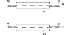
- FIG. 16 is a diagram schematically showing the circulation flow of the cooling water 22 in the cooler 15C. As shown in FIG. 16, the cooler 15C circulates the cooling water 22 in the cooling pipe 17C. By doing so, the cooler 15C cools the resin package module 12 via the metal base 16.
- the cooler 15C receives heat generated from the semiconductor element 3 and heat generated from the semiconductor element 4 transmitted through the metal block 1, the insulating material 9, the metal plate 10, and the thermal paste 13 in the resin package module 12. Heat is dissipated by the cooling water 22 circulating in the cooling pipe 17C via the metal base 16.
- the cooling pipe 17C of the cooler 15C is arranged so as to surround only the pair of opposite side surfaces of the resin package module 12 in a plan view, the height of the entire structure of the semiconductor device is kept low. be able to. Further, since the cooling pipe 17C is arranged so as not to surround the entire circumference of the resin package module 12 in a plan view, the occupied area (foot space) of the semiconductor device can be reduced.
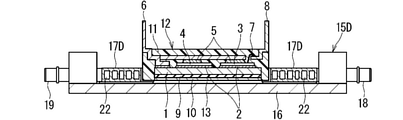
- FIG. 17 is a cross-sectional view schematically showing an example of the configuration of the semiconductor device according to the present embodiment.
- FIG. 18 is a cross-sectional view from another direction schematically showing an example of the configuration of the semiconductor device according to the present embodiment.
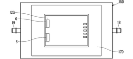
- FIG. 19 is a plan view schematically showing an example of the configuration of the semiconductor device according to the present embodiment.
- the semiconductor device includes a resin package module 12 and a cooler 15D that cools the resin package module 12 by water cooling.
- the cooler 15D made of aluminum or the like surrounds the resin package module 12 in a plan view and is arranged in contact with the lower surface of the resin package module 12, specifically, the lower surface of the metal plate 10.
- the cooler 15D is arranged on the metal base 16 made of copper or the like that contacts the lower surface of the metal plate 10 via the thermal paste 13, and on the upper surface of the metal base 16, and the entire resin package module 12 is arranged in a plan view.
- the inner side surface surrounding the resin package module 12 is in contact with the side surface of the resin package module 12 via thermal paste 13 (not shown) or the like.
- the cooling pipe 17D comes into contact with the side surface of the resin package module 12, it becomes difficult to secure the circular surface distance and the space distance of the main terminal 6 and the signal terminal 8 protruding from the side surface of the resin package module 12. In some cases, these terminals may be modified so as to protrude from the upper surface of the resin package module 12.
- the main terminal 6 and the signal terminal 8 are exposed at the corners of the upper surface of the mold resin 11 and are flush with the upper surface of the mold resin 11. It is formed so as to extend along. Then, the main terminal 6 and the signal terminal 8 are formed so as to extend upward from the corner portion of the upper surface of the mold resin 11 so as to be flush with the side surface of the mold resin 11.
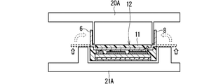
- FIG. 20 is a diagram showing an example of lead forming when the side surfaces of the mold resin 11 are not flush with each other.
- FIG. 21 is a diagram showing an example of lead forming when the upper surface and the side surface of the mold resin 11 are flush with each other.
- the main terminal 6 and the signal terminal 8 are bent by the lead forming die 20 arranged above and the lead forming die 21 arranged below, both of which are made of the mold resin 11. There is no one-sided relationship with the sides.
- the main terminal 6 and the signal terminal 8 are bent by the lead forming die 20A arranged above and the lead forming die 21A arranged below, and both are made of a mold resin. It is formed so as to extend upward while maintaining a flush relationship with the side surface of 11. Further, in the case shown in FIG. 21, the bent main terminal 6 and the signal terminal 8 are flush with the upper surface of the mold resin 11.
- FIG. 22 is a diagram schematically showing the circulation flow of the cooling water 22 in the cooler 15D. As shown in FIG. 22, the cooler 15D circulates the cooling water 22 in the cooling pipe 17D. By doing so, the cooler 15D cools the resin package module 12 via the metal base 16.
- the cooler 15D transfers heat generated from the semiconductor element 3 and heat generated from the semiconductor element 4 transmitted through the metal block 1, the insulating material 9, the metal plate 10, and the thermal paste 13 in the resin package module 12. Heat is dissipated by the cooling water 22 circulating in the cooling pipe 17D via the metal base 16.
- the cooler 15D has an inner side surface in which the heat generated from the semiconductor element 3 and the heat generated from the semiconductor element 4 transmitted through the metal block 1 and the mold resin 11 in the resin package module 12 come into contact with the resin package module 12. It is cooled by the cooling water 22 circulating in the cooling pipe 17D.
- the cooling pipe 17D of the cooler 15D is arranged so as to surround the resin package module 12 in a plan view, the height of the entire structure of the semiconductor device can be kept low. Further, since the cooler 15D cools the heat generated from the semiconductor element 3 and the heat generated from the semiconductor element 4 via the inner side surface in contact with the resin package module 12, the cooling efficiency is improved. Further, if the main terminal 6 and the signal terminal 8 are configured to protrude from the upper surface of the mold resin 11, the allowable range of the voltage applied to the semiconductor element 3 and the semiconductor element 4 is expanded, so that the quality of the semiconductor device is improved. do.
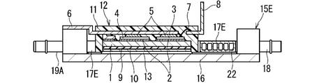
- FIG. 23 is a cross-sectional view schematically showing an example of the configuration of the semiconductor device according to the present embodiment.
- FIG. 24 is a cross-sectional view from another direction schematically showing an example of the configuration of the semiconductor device according to the present embodiment.
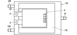
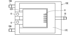
- FIG. 25 is a plan view schematically showing an example of the configuration of the semiconductor device according to the present embodiment.
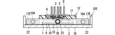
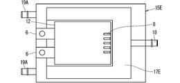
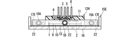
- the semiconductor device includes a resin package module 12 and a cooler 15E that cools the resin package module 12 by water cooling.
- the cooler 15E made of aluminum or the like surrounds the resin package module 12 in a plan view and is arranged in contact with the lower surface of the resin package module 12, specifically, the lower surface of the metal plate 10.
- the cooler 15E is arranged on the upper surface of the metal base 16 and the metal base 16 formed of copper or the like that contacts the lower surface of the metal plate 10 via the thermal paste 13, and partially comprises the resin package module 12 in a plan view.
- the cooling water introduction nipple 18 is provided on the straight portion of the cooling pipe 17E that partially surrounds the resin package module 12 in a plan view. Further, the two cooling water drainage nipples 19A are provided at both ends of the cooling pipe 17E that partially surrounds the resin package module 12 in a plan view.
- the inner side surface surrounding the resin package module 12 is in contact with the side surface of the resin package module 12 via thermal paste 13 (not shown) or the like.
- the signal terminal 8 is formed so as to be exposed at the corner of the upper surface of the mold resin 11 and extend along the upper surface so as to be flush with the upper surface of the mold resin 11. To. Then, the signal terminal 8 is formed so as to extend upward from the corner portion of the upper surface of the mold resin 11 so as to be flush with the side surface of the mold resin 11.
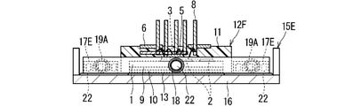
- FIG. 26 is a diagram schematically showing the circulation flow of the cooling water 22 in the cooler 15E. As shown in FIG. 26, the cooler 15E circulates the cooling water 22 in the cooling pipe 17E. By doing so, the cooler 15E cools the resin package module 12 via the metal base 16.
- the cooler 15E transfers heat generated from the semiconductor element 3 and heat generated from the semiconductor element 4 transmitted through the metal block 1, the insulating material 9, the metal plate 10, and the thermal paste 13 in the resin package module 12. Heat is dissipated by the cooling water 22 circulating in the cooling pipe 17E via the metal base 16.
- the cooler 15E has an inner side surface in which the heat generated from the semiconductor element 3 and the heat generated from the semiconductor element 4 transmitted through the metal block 1 and the mold resin 11 in the resin package module 12 come into contact with the resin package module 12. It is cooled by the cooling water 22 circulating in the cooling pipe 17E.
- the cooling pipe 17E of the cooler 15E is arranged so as to partially surround the resin package module 12 in a plan view, the height of the entire structure of the semiconductor device can be kept low. Further, since the cooler 15E cools the heat generated from the semiconductor element 3 and the heat generated from the semiconductor element 4 via the inner side surface in contact with the resin package module 12, the cooling efficiency is improved. Further, if the signal terminal 8 is configured to protrude from the upper surface of the mold resin 11, the allowable range of the voltage applied to the semiconductor element 3 and the semiconductor element 4 is expanded, so that the quality of the semiconductor device is improved. Further, since the cooling pipe 17E is arranged so as not to surround the entire circumference of the resin package module 12 in a plan view, the occupied area (foot space) of the semiconductor device can be reduced.
- FIG. 27 is a cross-sectional view schematically showing an example of the configuration of the semiconductor device according to the present embodiment.
- FIG. 28 is a cross-sectional view from another direction schematically showing an example of the configuration of the semiconductor device according to the present embodiment.
- FIG. 29 is a plan view schematically showing an example of the configuration of the semiconductor device according to the present embodiment.
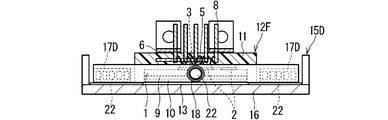
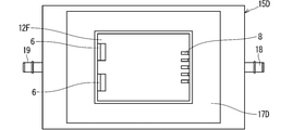
- the semiconductor device includes a resin package module 12F and a cooler 15D that cools the resin package module 12F by water cooling.
- the resin package module 12F includes a metal block 1F made of copper or the like, a semiconductor element 3 containing silicon (Si) or the like bonded to the upper surface of the metal block 1F via a brazing material 2 such as solder, and a metal block 1F.
- a semiconductor element 4 containing silicon (Si) or the like bonded to the upper surface of the semiconductor element 3 via a brazing material 2 such as solder, and bonded to the upper surface of the semiconductor element 3 and the upper surface of the semiconductor element 4 via a brazing material 5 such as solder.
- a main terminal 6 made of copper or the like, a signal terminal 8 made of copper or the like connected to a semiconductor element 3 via a wire bond 7 made of aluminum or the like, a part of the main terminal 6 and a signal. It includes a mold resin 11 formed by enclosing the above configuration while exposing a part of the terminal 8. Further, the lower surface of the metal block 1F is covered with the mold resin 11.
- the cooler 15D made of aluminum or the like is arranged in contact with the lower surface of the resin package module 12F, specifically, the lower surface of the mold resin 11 while surrounding the resin package module 12F in a plan view.
- the cooler 15D is arranged on the metal base 16 made of copper or the like that comes into contact with the lower surface of the mold resin 11 via the thermal paste 13, and on the upper surface of the metal base 16, and the entire resin package module 12F is arranged in a plan view.
- the inner side surface surrounding the resin package module 12F is in contact with the side surface of the resin package module 12F via thermal paste 13 (not shown) or the like.
- the cooler 15D is provided as a cooler for cooling the resin package module 12F, but even if the cooler 15 shown in another embodiment is provided instead. good.
- FIG. 30 is a diagram schematically showing the circulation flow of the cooling water 22 in the cooler 15D. As shown in FIG. 30, the cooler 15D circulates the cooling water 22 in the cooling pipe 17D. By doing so, the cooler 15D cools the resin package module 12F via the metal base 16.
- the cooler 15D cools the heat generated from the semiconductor element 3 and the heat generated from the semiconductor element 4 transmitted through the metal block 1F and the thermal paste 13 in the resin package module 12F via the metal base 16. Heat is dissipated by the cooling water 22 that circulates in the pipe 17D.
- the cooler 15D has an inner side surface in which the heat generated from the semiconductor element 3 and the heat generated from the semiconductor element 4 transmitted through the metal block 1F and the mold resin 11 in the resin package module 12F come into contact with the resin package module 12F. It is cooled by the cooling water 22 circulating in the cooling pipe 17D.
- the cooling pipe 17D of the cooler 15D is arranged so as to surround the resin package module 12F in a plan view, the height of the entire structure of the semiconductor device can be kept low. Further, since the cooler 15D cools the heat generated from the semiconductor element 3 and the heat generated from the semiconductor element 4 via the inner side surface in contact with the resin package module 12F, the cooling efficiency is improved. Further, since the lower surface of the metal block 1F is covered with the mold resin 11 and the resin package module 12F has a sufficient withstand voltage, the resin package module 12F does not need to have a separate insulating material. Therefore, it is possible to improve the assembleability of the semiconductor device and suppress the manufacturing cost.
- FIG. 31 is a cross-sectional view schematically showing an example of the configuration of the semiconductor device according to the present embodiment.
- FIG. 32 is a cross-sectional view from another direction schematically showing an example of the configuration of the semiconductor device according to the present embodiment.
- FIG. 33 is a plan view schematically showing an example of the configuration of the semiconductor device according to the present embodiment.
- the semiconductor device includes a resin package module 12F and a cooler 15E that cools the resin package module 12F by water cooling.
- the resin package module 12F includes a metal block 1F, a semiconductor element 3, a semiconductor element 4, a main terminal 6, a signal terminal 8, and a mold resin 11.
- the cooler 15E is arranged in contact with the lower surface of the resin package module 12F, specifically, the lower surface of the mold resin 11 while surrounding the resin package module 12F in a plan view.
- the cooler 15E includes a metal base 16, a cooling pipe 17E, a cooling water introduction nipple 18, and two cooling water drainage nipples 19A.
- the cooling water introduction nipple 18 is provided on the straight portion of the cooling pipe 17E that partially surrounds the resin package module 12F in a plan view. Further, the two cooling water drainage nipples 19A are provided at both ends of the cooling pipe 17E that partially surrounds the resin package module 12F in a plan view.
- the inner side surface surrounding the resin package module 12F is in contact with the side surface of the resin package module 12F via a thermal paste 13 (not shown) or the like.
- the cooler 15E is provided as a cooler for cooling the resin package module 12F, but even if the cooler 15A shown in another embodiment is provided instead. good.
- FIG. 34 is a diagram schematically showing the circulation flow of the cooling water 22 in the cooler 15E.
- the cooler 15E circulates the cooling water 22 in the cooling pipe 17E. By doing so, the cooler 15E cools the resin package module 12F via the metal base 16.
- the cooler 15E cools the heat generated from the semiconductor element 3 and the heat generated from the semiconductor element 4 transmitted through the metal block 1 and the thermal paste 13 in the resin package module 12F via the metal base 16. Heat is dissipated by the cooling water 22 that circulates in the pipe 17E.
- the cooler 15E has an inner side surface in which the heat generated from the semiconductor element 3 and the heat generated from the semiconductor element 4 transmitted through the metal block 1 and the mold resin 11 in the resin package module 12F come into contact with the resin package module 12F. It is cooled by the cooling water 22 that circulates in the cooling pipe 17E.
- the cooling pipe 17E of the cooler 15E is arranged so as to partially surround the resin package module 12F in a plan view, the height of the entire structure of the semiconductor device can be kept low. Further, since the cooler 15E cools the heat generated from the semiconductor element 3 and the heat generated from the semiconductor element 4 via the inner side surface in contact with the resin package module 12F, the cooling efficiency is improved. Further, since the lower surface of the metal block 1F is covered with the mold resin 11 and the resin package module 12F has a sufficient withstand voltage, the resin package module 12F does not need to have a separate insulating material. Therefore, the assemblability of the semiconductor device can be improved and the manufacturing cost can be suppressed.
- FIG. 35 is a cross-sectional view schematically showing an example of the configuration of the semiconductor device according to the present embodiment.
- FIG. 36 is a cross-sectional view from another direction schematically showing an example of the configuration of the semiconductor device according to the present embodiment.
- FIG. 37 is a plan view schematically showing an example of the configuration of the semiconductor device according to the present embodiment.
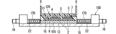
- the semiconductor device includes a resin package module 12G and a cooler 15D that cools the resin package module 12G by water cooling.
- the resin package module 12G includes a metal block 1G made of copper or the like, a semiconductor element 3 containing silicon (Si) or the like bonded to the upper surface of the metal block 1G via a brazing material 2 such as solder, and a metal block 1G.
- a semiconductor element 4 containing silicon (Si) or the like bonded to the upper surface of the semiconductor element 3 via a brazing material 2 such as solder, and bonded to the upper surface of the semiconductor element 3 and the upper surface of the semiconductor element 4 via a brazing material 5 such as solder. It is provided on the lower surface of the metal block 1G, the main terminal 6 made of copper or the like, the signal terminal 8 made of copper or the like connected to the semiconductor element 3 via a wire bond 7 made of aluminum or the like.
- the cooler 15D made of aluminum or the like surrounds the resin package module 12G in a plan view and is arranged in contact with the lower surface of the resin package module 12G, specifically, the lower surface of the metal plate 10G.
- the cooler 15D is arranged on the metal base 16 made of copper or the like that contacts the lower surface of the metal plate 10G via the thermal paste 13, and on the upper surface of the metal base 16, and is the entire resin package module 12G in a plan view.
- the inner side surface surrounding the resin package module 12G is in contact with the side surface of the metal plate 10G via a thermal paste 13 (not shown) or the like.
- FIG. 38 is a diagram schematically showing the circulation flow of the cooling water 22 in the cooler 15D.
- the cooler 15D circulates the cooling water 22 in the cooling pipe 17D. By doing so, the cooler 15D cools the resin package module 12G via the metal base 16.
- the cooler 15D transfers the heat generated from the semiconductor element 3 and the heat generated from the semiconductor element 4 transmitted through the metal block 1G, the insulating material 9, the metal plate 10G, and the thermal paste 13 in the resin package module 12G. Heat is dissipated by the cooling water 22 circulating in the cooling pipe 17D via the metal base 16.
- the cooler 15D contacts the resin package module 12G with the heat generated from the semiconductor element 3 and the heat generated from the semiconductor element 4 transmitted through the metal block 1G, the insulating material 9, and the metal plate 10G in the resin package module 12G. It is cooled by the cooling water 22 circulating in the cooling pipe 17D via the inner side surface.
- the cooling pipe 17D of the cooler 15D is arranged so as to surround the resin package module 12G in a plan view, the height of the entire structure of the semiconductor device can be kept low. Further, since the cooler 15D cools the heat generated from the semiconductor element 3 and the heat generated from the semiconductor element 4 via the inner side surface in contact with the side surface of the metal plate 10G of the resin package module 12G, the cooling efficiency is improved.
- FIG. 39 is a cross-sectional view schematically showing an example of the configuration of the semiconductor device according to the present embodiment.
- FIG. 40 is a cross-sectional view from another direction schematically showing an example of the configuration of the semiconductor device according to the present embodiment.
- FIG. 41 is a plan view schematically showing an example of the configuration of the semiconductor device according to the present embodiment.
- the semiconductor device includes a resin package module 12H and a cooler 15E that cools the resin package module 12H by water cooling.
- the resin package module 12H includes a metal block 1H made of copper or the like, a semiconductor element 3 containing silicon (Si) or the like bonded to the upper surface of the metal block 1H via a brazing material 2 such as solder, and a metal block 1H.
- a semiconductor element 4 containing silicon (Si) or the like bonded to the upper surface of the semiconductor element 3 via a brazing material 2 such as solder, and bonded to the upper surface of the semiconductor element 3 and the upper surface of the semiconductor element 4 via a brazing material 5 such as solder. It is provided on the lower surface of the metal block 1H, the main terminal 6 made of copper or the like, the signal terminal 8 made of copper or the like connected to the semiconductor element 3 via a wire bond 7 made of aluminum or the like.
- the cooler 15E is arranged in contact with the lower surface of the resin package module 12H, specifically, the lower surface of the metal plate 10H, while surrounding the resin package module 12H in a plan view.
- the cooler 15E includes a metal base 16 made of copper or the like that contacts the lower surface of the metal plate 10H via a thermal paste 13, a cooling pipe 17E, a cooling water introduction nipple 18, and two cooling water drainage nipples 19A. To prepare for.
- the cooling water introduction nipple 18 is provided on the straight portion of the cooling pipe 17E that partially surrounds the resin package module 12H in a plan view. Further, the two cooling water drainage nipples 19A are provided at both ends of the cooling pipe 17E that partially surrounds the resin package module 12H in a plan view.
- the inner side surface surrounding the resin package module 12H is in contact with the side surface of the metal plate 10H via a thermal paste 13 (not shown) or the like.
- FIG. 42 is a diagram schematically showing the circulation flow of the cooling water 22 in the cooler 15E.
- the cooler 15E circulates the cooling water 22 in the cooling pipe 17E. By doing so, the cooler 15E cools the resin package module 12H via the metal base 16.
- the cooler 15E transfers the heat generated from the semiconductor element 3 and the heat generated from the semiconductor element 4 transmitted through the metal block 1H, the insulating material 9, the metal plate 10H, and the thermal paste 13 in the resin package module 12H. Heat is dissipated by the cooling water 22 circulating in the cooling pipe 17E via the metal base 16.
- the cooler 15E contacts the resin package module 12H with the heat generated from the semiconductor element 3 and the heat generated from the semiconductor element 4 transmitted through the metal block 1H, the insulating material 9, and the metal plate 10H in the resin package module 12H. It is cooled by the cooling water 22 circulating in the cooling pipe 17E via the inner side surface.
- the cooling pipe 17E of the cooler 15E is arranged so as to partially surround the resin package module 12H in a plan view, the height of the entire structure of the semiconductor device can be kept low. Further, since the cooler 15E cools the heat generated from the semiconductor element 3 and the heat generated from the semiconductor element 4 via the inner side surface in contact with the side surface of the metal plate 10H of the resin package module 12H, the cooling efficiency is improved. Further, since the cooling pipe 17E is arranged so as not to surround the entire circumference of the resin package module 12H in a plan view, the occupied area (foot space) of the semiconductor device can be reduced.
- FIG. 43 is a cross-sectional view schematically showing an example of the configuration of the semiconductor device according to the present embodiment.
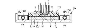
- FIG. 44 is a cross-sectional view from another direction schematically showing an example of the configuration of the semiconductor device according to the present embodiment.
- FIG. 45 is a plan view schematically showing an example of the configuration of the semiconductor device according to the present embodiment.
- the semiconductor device includes a resin package module 12J and a cooler 15C for cooling the resin package module 12J by water cooling.
- the resin package module 12J includes a metal block 1J made of copper or the like, a semiconductor element 3 containing silicon (Si) or the like bonded to the upper surface of the metal block 1J via a brazing material 2 such as solder, and a metal block 1J.
- a semiconductor element 4 containing silicon (Si) or the like bonded to the upper surface of the semiconductor element 3 via a brazing material 2 such as solder, and bonded to the upper surface of the semiconductor element 3 and the upper surface of the semiconductor element 4 via a brazing material 5 such as solder.
- a part of the side surface of the plate 10J (that is, the side surface of the cooler 15C facing the cooling pipe 17C) and the lower surface are exposed, and the mold resin 11 formed by enclosing the above configuration is provided.
- the main terminal 6 and the signal terminal 8 each project from the side surface of the mold resin 11.
- the cooler 15C made of aluminum or the like surrounds the resin package module 12J in a plan view and is arranged in contact with the lower surface of the resin package module 12J, specifically, the lower surface of the metal plate 10J.
- the cooler 15C is arranged on a metal base 16 made of copper or the like that contacts the lower surface of the metal plate 10J via a thermal paste 13, and a resin package module 12J in a plan view.
- Cooling pipe 17C made of aluminum or the like arranged so as to surround the surface, cooling water introduction nipple 18C for introducing cooling water 22 into the cooling pipe 17C, and cooling water drainage nipple 19C for discharging cooling water 22 from the cooling pipe 17C. And prepare.
- FIG. 46 is a diagram schematically showing the circulation flow of the cooling water 22 in the cooler 15C. As shown in FIG. 46, the cooler 15C circulates the cooling water 22 in the cooling pipe 17C. By doing so, the cooler 15C cools the resin package module 12J via the metal base 16.
- the cooler 15C transfers heat generated from the semiconductor element 3 and heat generated from the semiconductor element 4 transmitted through the metal block 1, the insulating material 9, the metal plate 10J, and the thermal paste 13 in the resin package module 12J. Heat is dissipated by the cooling water 22 circulating in the cooling pipe 17C via the metal base 16.
- the cooler 15C contacts the resin package module 12J with the heat generated from the semiconductor element 3 and the heat generated from the semiconductor element 4 transmitted through the metal block 1J, the insulating material 9, and the metal plate 10J in the resin package module 12J. It is cooled by the cooling water 22 circulating in the cooling pipe 17C via the inner side surface.
- the cooling pipe 17C of the cooler 15C is arranged so as to surround only the pair of opposite side surfaces of the resin package module 12J in a plan view, the height of the entire structure of the semiconductor device is kept low. be able to. Further, since the cooling pipe 17C is arranged so as not to surround the entire circumference of the resin package module 12J in a plan view, the occupied area (foot space) of the semiconductor device can be reduced.
- the replacement may be made across a plurality of embodiments. That is, it may be the case that the respective configurations shown in the examples in different embodiments are combined to produce the same effect.
- the semiconductor device includes a semiconductor module and a cooler 15 for cooling the semiconductor module.
- the semiconductor module corresponds to, for example, any one of a resin package module 12, a resin package module 12F, a resin package module 12G, a resin package module 12H, a resin package module 12J, and the like (hereinafter, the module corresponds to any one of them). For convenience, any one of these may be described in association with each other).
- the resin package module 12 includes a metal block 1 (or a metal block 1F, a metal block 1G, a metal block 1H, a metal block 1J), a semiconductor element 3 (or a semiconductor element 4) provided on the upper surface of the metal block 1, and a semiconductor element 3 (or a semiconductor element 4).
- a terminal connected to the semiconductor element 3 and a part of the terminal, a metal block 1, and a resin covering the semiconductor element 3 are provided.
- the terminal corresponds to, for example, any one of the main terminal 6 and the signal terminal 8 (hereinafter, for convenience, any one of these is described in correspondence with each other).
- the resin corresponds to, for example, the mold resin 11.
- the cooler 15 includes a metal base 16 and a cooling pipe 17 (or a cooling pipe 17A, a cooling pipe 17B, a cooling pipe 17C, a cooling pipe 17D, and a cooling pipe 17E).
- the metal base 16 contacts the lower surface of the resin package module 12. Further, the metal base 16 is provided in a region larger than the region overlapping the resin package module 12 in a plan view.
- the cooling pipe 17 is arranged on the upper surface of the metal base 16. Further, the cooling pipe 17 circulates a refrigerant for cooling the resin package module 12.
- the refrigerant corresponds to, for example, cooling water 22 and the like.
- the cooling pipe 17 is provided so as to surround at least a part of the resin package module 12 in a plan view.
- the cooling pipe 17 of the cooler 15 is arranged so as to surround the resin package module 12 in a plan view, the height of the entire structure of the semiconductor device can be kept low. Specifically, the heat generated from the semiconductor element 3 and the semiconductor element 4 in the resin package module 12 is transferred through the metal block 1, the insulating material 9, the metal plate 10, the thermal paste 13, and the metal base 16 in the resin package module 12. By radiating heat to the lower surface of the cooling pipe 17, it is not necessary to arrange the cooling pipe below the resin package module 12, so that the height of the entire structure of the semiconductor device can be kept low. When securing foot space and improving cooling capacity were prioritized, the cooling pipe was placed below the resin package module, which was a factor in increasing the height of the entire structure of the semiconductor device.
- the height of the entire semiconductor device structure can be increased even if the foot space or cooling capacity is sacrificed to some extent. In some cases, it was required to keep it low. According to the above configuration, such a request can be met.
- the lower surface of the metal block 1F is covered with the mold resin 11. Then, the metal base 16 comes into contact with the lower surface of the mold resin 11. According to such a configuration, since the lower surface of the metal block 1F is covered with the mold resin 11 and the resin package module 12F has a sufficient dielectric strength, the resin package module 12F does not need to have a separate insulating material. Therefore, it is possible to improve the assembleability of the semiconductor device and suppress the manufacturing cost.
- the resin package module 12 includes an insulating material 9 provided on the lower surface of the metal block 1 and a metal plate 10 provided on the lower surface of the insulating material 9. Then, the lower surface of the metal plate 10 is exposed from the mold resin 11. Further, the metal base 16 comes into contact with the lower surface of the metal plate 10. According to such a configuration, since the upper surface of the metal base 16 and the lower surface of the metal plate 10 are in contact with each other via the thermal paste 13, the heat generated from the semiconductor element 3 and the heat generated from the semiconductor element 4 are effectively used. Can be cooled.
- the cooler 15D cools the heat generated from the semiconductor element 3 and the heat generated from the semiconductor element 4 through the inner side surface in contact with the side surface of the metal plate 10G of the resin package module 12G. Cooling efficiency is improved.
- the main terminal 6 (or the signal terminal 8) extends from the upper surface of the mold resin 11. According to such a configuration, the allowable range of the voltage applied to the semiconductor element 3 and the semiconductor element 4 is expanded by increasing the insulation distance, so that the quality of the semiconductor device is improved.
- the main terminal 6 (or the signal terminal 8) has a portion extending flush with the upper surface on the upper surface of the mold resin 11. According to such a configuration, the allowable range of the voltage applied to the semiconductor element 3 and the semiconductor element 4 is expanded by increasing the insulation distance, so that the quality of the semiconductor device is improved.
- the main terminal 6 (or the signal terminal 8) has a portion extending on the upper surface of the mold resin 11 so as to be flush with the side surface of the mold resin 11. According to such a configuration, the allowable range of the voltage applied to the semiconductor element 3 and the semiconductor element 4 is expanded by increasing the insulation distance, so that the quality of the semiconductor device is improved.
- the cooling pipe 17D contacts the side surface of the resin package module 12. According to such a configuration, the cooler 15D cools the heat generated from the semiconductor element 3 and the heat generated from the semiconductor element 4 via the inner side surface in contact with the resin package module 12, so that the cooling efficiency is improved.
- the cooling pipe 17 is provided so as to surround the entire circumference of the resin package module 12 in a plan view. According to such a configuration, the resin package module 12 can be effectively cooled.
- the cooling pipe 17A is provided so as to surround only a part of the side surface of the resin package module 12 in a plan view. According to such a configuration, since the cooling pipe 17A is arranged so as not to surround the entire circumference of the resin package module 12 in a plan view, the occupied area (foot space) of the semiconductor device can be reduced.
- the cooling pipe 17B has nipples at both ends in the longitudinal direction of the cooling pipe 17B.
- the nipple corresponds to, for example, any one of the cooling water introduction nipple 18B and the cooling water drainage nipple 19B. According to such a configuration, since the nipple is not provided in the straight portion of the cooling pipe 17B, it is possible to suppress the manufacturing cost or improve the assembling property.
- the cooling pipe 17C is provided so as to surround only the pair of opposite side surfaces of the resin package module 12 in a plan view. According to such a configuration, since the cooling pipe 17C is arranged so as to surround only a pair of facing side surfaces without surrounding the entire circumference of the resin package module 12 in a plan view, the occupied area (foot space) of the semiconductor device is provided. Can be reduced.
- a wide bandgap semiconductor is used for the semiconductor element 3. According to such a configuration, the allowable range of the operating temperature of the semiconductor element is extended by using the wide bandgap semiconductor. Therefore, the tolerance for heat generation imbalance in the semiconductor element and between the semiconductor elements is improved. Therefore, since the required cooling capacity of the cooler is reduced, the cooler can be made compact, and as a result, the size of the semiconductor device can be suppressed.
- the material when the material name or the like is described without being specified, the material contains other additives, for example, an alloy or the like, as long as there is no contradiction. It shall be included.
- each component in the embodiments described above is a conceptual unit, and within the scope of the technique disclosed herein, one component comprises a plurality of structures. It is assumed that one component corresponds to a part of a structure, and further, a case where a plurality of components are provided in one structure is included.
- each component in the above-described embodiment shall include a structure having another structure or shape as long as it exhibits the same function.
Landscapes
- Cooling Or The Like Of Semiconductors Or Solid State Devices (AREA)
- Engineering & Computer Science (AREA)
- Chemical & Material Sciences (AREA)
- Ceramic Engineering (AREA)
- Microelectronics & Electronic Packaging (AREA)
Abstract
半導体装置の高さを低く抑えつつ、半導体装置の放熱を効果的に行う。半導体装置は、半導体モジュールを冷却する冷却器を備え、半導体モジュールは、金属ブロックと、半導体素子と、半導体素子に接続される端子と、端子の一部、金属ブロック、半導体素子を覆う樹脂とを備え、冷却器は、半導体モジュールの下面に接触し、平面視において半導体モジュールを含む金属ベースと、金属ベースの上面に配置され、半導体モジュールを冷却する冷却配管とを備え、冷却配管は、平面視において半導体モジュールを少なくとも一部囲む。
Description
本願明細書に開示される技術は、半導体装置に関するものである。
たとえば特許文献1には、冷却器に接合された半導体モジュールを有する半導体装置が開示されている。当該半導体モジュールは、モールド樹脂の下面から露出する金属ブロックを介して冷却器と接触し、生じる熱を放熱する。
特許文献1に示される技術では、アルミなどで形成される水冷のための冷却器は、半導体装置の下面に配置される。そのため、半導体装置の構造全体の高さが増すという問題がある。
本願明細書に開示される技術は、以上に記載されたような問題を鑑みてなされたものであり、半導体装置の高さを低く抑えつつ、半導体装置の放熱を効果的に行うための技術である。
本願明細書に開示される技術の第1の態様である半導体装置は、半導体モジュールと、前記半導体モジュールを冷却する冷却器とを備え、前記半導体モジュールは、金属ブロックと、前記金属ブロックの上面に設けられる半導体素子と、前記半導体素子に接続される端子と、前記端子の一部、前記金属ブロックおよび前記半導体素子を覆う樹脂とを備え、前記冷却器は、前記半導体モジュールの下面に接触しつつ、平面視において前記半導体モジュールを含む領域に設けられる金属ベースと、前記金属ベースの上面に配置され、かつ、前記半導体モジュールを冷却するための冷媒を循環させる冷却配管とを備え、前記冷却配管は、平面視において前記半導体モジュールを少なくとも一部囲んで設けられる。
本願明細書に開示される技術の少なくとも第1の態様によれば、冷却器の冷却配管が平面視で半導体モジュールを囲んで配置されるため、半導体装置の構造全体の高さを低く抑えることができる。
また、本願明細書に開示される技術に関連する目的と、特徴と、局面と、利点とは、以下に示される詳細な説明と添付図面とによって、さらに明白となる。
以下、添付される図面を参照しながら実施の形態について説明する。以下の実施の形態では、技術の説明のために詳細な特徴なども示されるが、それらは例示であり、実施の形態が実施可能となるためにそれらすべてが必ずしも必須の特徴ではない。
なお、図面は概略的に示されるものであり、説明の便宜のため、適宜、構成の省略、または、構成の簡略化が図面においてなされるものである。また、異なる図面にそれぞれ示される構成などの大きさおよび位置の相互関係は、必ずしも正確に記載されるものではなく、適宜変更され得るものである。また、断面図ではない平面図などの図面においても、実施の形態の内容を理解することを容易にするために、ハッチングが付される場合がある。
また、以下に示される説明では、同様の構成要素には同じ符号を付して図示し、それらの名称と機能とについても同様のものとする。したがって、それらについての詳細な説明を、重複を避けるために省略する場合がある。
また、以下に記載される説明において、ある構成要素を「備える」、「含む」または「有する」などと記載される場合、特に断らない限りは、他の構成要素の存在を除外する排他的な表現ではない。
また、以下に記載される説明において、「第1の」または「第2の」などの序数が用いられる場合があっても、これらの用語は、実施の形態の内容を理解することを容易にするために便宜上用いられるものであり、これらの序数によって生じ得る順序などに限定されるものではない。
また、以下に記載される説明において、等しい状態であることを示す表現、たとえば、「同一」、「等しい」、「均一」または「均質」などは、特に断らない限りは、厳密に等しい状態であることを示す場合、および、公差または同程度の機能が得られる範囲において差が生じている場合を含むものとする。
また、以下に記載される説明において、「上」、「下」、「左」、「右」、「側」、「底」、「表」または「裏」などの特定の位置または方向を意味する用語が用いられる場合があっても、これらの用語は、実施の形態の内容を理解することを容易にするために便宜上用いられるものであり、実際に実施される際の位置または方向とは関係しないものである。
また、以下に記載される説明において、「…の上面」または「…の下面」などと記載される場合、対象となる構成要素の上面自体または下面自体に加えて、対象となる構成要素の上面または下面に他の構成要素が形成された状態も含むものとする。すなわち、たとえば、「甲の上面に設けられる乙」と記載される場合、甲と乙との間に別の構成要素「丙」が介在することを妨げるものではない。
<第1の実施の形態>
以下、本実施の形態に関する半導体装置について説明する。説明の便宜上、まず、発明者が知っている半導体装置の構成に関する技術について説明する。
以下、本実施の形態に関する半導体装置について説明する。説明の便宜上、まず、発明者が知っている半導体装置の構成に関する技術について説明する。
図47は、本実施の形態に関する半導体装置の構成の例を概略的に示す断面図である。また、図48は、本実施の形態に関する半導体装置の構成の例を概略的に示す他の方向からの断面図である。また、図49は、本実施の形態に関する半導体装置の構成の例を概略的に示す平面図である。
図47、図48および図49に例が示されるように、半導体装置は、樹脂パッケージモジュール12と、水冷によって樹脂パッケージモジュール12を冷却する冷却器15Kとを備える。
樹脂パッケージモジュール12は、銅などで形成された金属ブロック1と、金属ブロック1の上面にはんだなどのロウ材2を介して接合されたシリコン(Si)などを含む半導体素子3と、金属ブロック1の上面にはんだなどのロウ材2を介して接合されたシリコン(Si)などを含む半導体素子4と、半導体素子3の上面および半導体素子4の上面にはんだなどのロウ材5を介して接合された銅などで形成された主端子6と、半導体素子3にアルミなどで形成されたワイヤーボンド7を介して接続された銅などで形成された信号端子8と、金属ブロック1の下面に設けられたエポキシ樹脂またはセラミックなどで形成された絶縁材9と、絶縁材9の下面に設けられた銅などで形成された金属板10と、主端子6の一部、信号端子8の一部および金属板10の下面を露出させつつ、上記の構成を封入して形成されたモールド樹脂11とを備える。ここで、主端子6と信号端子8とは、それぞれモールド樹脂11の側面から突出する。
アルミなどで形成された冷却器15Kは、平面視で樹脂パッケージモジュール12と重なる位置に配置されつつ、樹脂パッケージモジュール12の下面、具体的には、金属板10の下面に接触して配置される。
冷却器15Kは、金属板10の下面に放熱グリス13を介して接触する銅などで形成された金属ベース14と、金属ベース14内の冷却配管に冷却水22を導入する冷却水導入ニップル18と、金属ベース14内の冷却配管から冷却水22を排出する冷却水排水ニップル19とを備える。
図50は、冷却器15Kにおける冷却水22の循環の流れを概略的に示す図である。図50に例が示されるように、冷却器15Kは、金属ベース14内の冷却配管に冷却水22を循環させる。そうすることによって、冷却器15Kは、金属ベース14を介して樹脂パッケージモジュール12を冷却する。
<半導体装置の構成について>
図1は、本実施の形態に関する半導体装置の構成の例を概略的に示す断面図である。また、図2は、本実施の形態に関する半導体装置の構成の例を概略的に示す他の方向からの断面図である。また、図3は、本実施の形態に関する半導体装置の構成の例を概略的に示す平面図である。
図1は、本実施の形態に関する半導体装置の構成の例を概略的に示す断面図である。また、図2は、本実施の形態に関する半導体装置の構成の例を概略的に示す他の方向からの断面図である。また、図3は、本実施の形態に関する半導体装置の構成の例を概略的に示す平面図である。
図1、図2および図3に例が示されるように、半導体装置は、樹脂パッケージモジュール12と、水冷によって樹脂パッケージモジュール12を冷却する冷却器15とを備える。
樹脂パッケージモジュール12は、銅などで形成された金属ブロック1と、金属ブロック1の上面にはんだなどのロウ材2を介して接合されたシリコン(Si)などを含む半導体素子3と、金属ブロック1の上面にはんだなどのロウ材2を介して接合されたシリコン(Si)などを含む半導体素子4と、半導体素子3の上面および半導体素子4の上面にはんだなどのロウ材5を介して接続された銅などで形成された主端子6と、半導体素子3にアルミなどで形成されたワイヤーボンド7を介して接続された銅などで形成された信号端子8と、金属ブロック1の下面に設けられたエポキシ樹脂またはセラミックなどで形成された絶縁材9と、絶縁材9の下面に設けられた銅などで形成された金属板10と、主端子6の一部、信号端子8の一部および金属板10の下面を露出させつつ、上記の構成を封入して形成されたモールド樹脂11とを備える。ここで、主端子6と信号端子8とは、それぞれモールド樹脂11の側面から突出する。
アルミなどで形成された冷却器15は、平面視で樹脂パッケージモジュール12を囲みつつ、樹脂パッケージモジュール12の下面、具体的には、金属板10の下面に接触して配置される。
冷却器15は、平面視において樹脂パッケージモジュール12と重なる領域よりも大きな領域に設けられ、かつ、金属板10の下面に放熱グリス13を介して接触する銅などで形成された金属ベース16と、金属ベース16の上面に配置され、かつ、平面視で樹脂パッケージモジュール12の全周囲を囲んで配置されるアルミなどで形成された冷却配管17と、冷却配管17に冷却水22を導入する冷却水導入ニップル18と、冷却配管17から冷却水22を排出する冷却水排水ニップル19とを備える。なお、本実施の形態における冷却器15は、冷却配管17において循環する冷却水22の水冷によって樹脂パッケージモジュール12を冷却するものであるが、冷却配管17において循環する気体の空冷などの他の冷媒を用いる方法によって樹脂パッケージモジュール12を冷却するものであってもよい。このことは、他の実施の形態における冷却器についても同様である。
図4は、冷却器15における冷却水22の循環の流れを概略的に示す図である。図4に例が示されるように、冷却器15は、冷却配管17に冷却水22を循環させる。そうすることによって、冷却器15は、金属ベース16を介して樹脂パッケージモジュール12を冷却する。
具体的には、冷却器15は、樹脂パッケージモジュール12における金属ブロック1、絶縁材9、金属板10、放熱グリス13を介して伝わる、半導体素子3から生じる熱および半導体素子4から生じる熱を、金属ベース16を介して、冷却配管17において循環する冷却水22によって放熱する。
なお、半導体素子3は、たとえば、絶縁ゲート型バイポーラトランジスタ(insulated gate bipolar transistor、すなわち、IGBT)または金属-酸化膜-半導体電界効果トランジスタ(metal-oxide-semiconductor field-effect transistor、すなわち、MOSFET)などである。また、半導体素子4は、たとえば、ダイオードなどである。
また、半導体素子3および半導体素子4に用いられる半導体としては、シリコン(Si)のほかに、たとえば、シリコンカーバイド(SiC)などのワイドバンドギャップ半導体が想定される。ここで、ワイドバンドギャップ半導体とは、一般に、およそ2eV以上の禁制帯幅をもつ半導体を指し、窒化ガリウム(GaN)などの3族窒化物、酸化亜鉛(ZnO)などの2族酸化物、セレン化亜鉛(ZnSe)などの2族カルコゲナイド、ダイヤモンドおよび炭化珪素などが知られる。本実施形態では炭化珪素を用いた場合を説明するが、他の半導体およびワイドバンドギャップ半導体であっても、同様に適用できる。
上記のような構成によれば、冷却器15の冷却配管17が平面視で樹脂パッケージモジュール12を囲んで配置されるため、半導体装置の構造全体の高さを低く抑えることができる。
<第2の実施の形態>
本実施の形態に関する半導体装置について説明する。なお、以下の説明においては、以上に記載された実施の形態で説明された構成要素と同様の構成要素については同じ符号を付して図示し、その詳細な説明については適宜省略するものとする。
本実施の形態に関する半導体装置について説明する。なお、以下の説明においては、以上に記載された実施の形態で説明された構成要素と同様の構成要素については同じ符号を付して図示し、その詳細な説明については適宜省略するものとする。
<半導体装置の構成について>
図5は、本実施の形態に関する半導体装置の構成の例を概略的に示す断面図である。また、図6は、本実施の形態に関する半導体装置の構成の例を概略的に示す他の方向からの断面図である。また、図7は、本実施の形態に関する半導体装置の構成の例を概略的に示す平面図である。
図5は、本実施の形態に関する半導体装置の構成の例を概略的に示す断面図である。また、図6は、本実施の形態に関する半導体装置の構成の例を概略的に示す他の方向からの断面図である。また、図7は、本実施の形態に関する半導体装置の構成の例を概略的に示す平面図である。
図5、図6および図7に例が示されるように、半導体装置は、樹脂パッケージモジュール12と、水冷によって樹脂パッケージモジュール12を冷却する冷却器15Aとを備える。
アルミなどで形成された冷却器15Aは、平面視で樹脂パッケージモジュール12を囲みつつ、樹脂パッケージモジュール12の下面、具体的には、金属板10の下面に接触して配置される。
冷却器15Aは、金属板10の下面に放熱グリス13を介して接触する銅などで形成された金属ベース16と、金属ベース16の上面に配置され、かつ、平面視で樹脂パッケージモジュール12を部分的に(すなわち、一部の側面のみを)囲んで配置されるアルミなどで形成された冷却配管17Aと、冷却配管17Aに冷却水22を導入する冷却水導入ニップル18と、冷却配管17Aから冷却水22を排出する2つの冷却水排水ニップル19Aとを備える。
冷却水導入ニップル18は、平面視で樹脂パッケージモジュール12を部分的に囲む冷却配管17Aの直線部に設けられる。また、2つの冷却水排水ニップル19Aは、平面視で樹脂パッケージモジュール12を部分的に囲む冷却配管17Aの両端に設けられる。
図8は、冷却器15Aにおける冷却水22の循環の流れを概略的に示す図である。図8に例が示されるように、冷却器15Aは、冷却配管17Aに冷却水22を循環させる。そうすることによって、冷却器15Aは、金属ベース16を介して樹脂パッケージモジュール12を冷却する。
具体的には、冷却器15Aは、樹脂パッケージモジュール12における金属ブロック1、絶縁材9、金属板10、放熱グリス13を介して伝わる、半導体素子3から生じる熱および半導体素子4から生じる熱を、金属ベース16を介して、冷却配管17Aにおいて循環する冷却水22によって放熱する。
上記のような構成によれば、冷却器15Aの冷却配管17Aが平面視で樹脂パッケージモジュール12を部分的に囲んで配置されるため、半導体装置の構造全体の高さを低く抑えることができる。また、冷却配管17Aが平面視で樹脂パッケージモジュール12の全周を囲まずに配置されているため、半導体装置の占有面積(フットスペース)を削減することができる。
<第3の実施の形態>
本実施の形態に関する半導体装置について説明する。なお、以下の説明においては、以上に記載された実施の形態で説明された構成要素と同様の構成要素については同じ符号を付して図示し、その詳細な説明については適宜省略するものとする。
本実施の形態に関する半導体装置について説明する。なお、以下の説明においては、以上に記載された実施の形態で説明された構成要素と同様の構成要素については同じ符号を付して図示し、その詳細な説明については適宜省略するものとする。
<半導体装置の構成について>
図9は、本実施の形態に関する半導体装置の構成の例を概略的に示す断面図である。また、図10は、本実施の形態に関する半導体装置の構成の例を概略的に示す他の方向からの断面図である。また、図11は、本実施の形態に関する半導体装置の構成の例を概略的に示す平面図である。
図9は、本実施の形態に関する半導体装置の構成の例を概略的に示す断面図である。また、図10は、本実施の形態に関する半導体装置の構成の例を概略的に示す他の方向からの断面図である。また、図11は、本実施の形態に関する半導体装置の構成の例を概略的に示す平面図である。
図9、図10および図11に例が示されるように、半導体装置は、樹脂パッケージモジュール12と、水冷によって樹脂パッケージモジュール12を冷却する冷却器15Bとを備える。
アルミなどで形成された冷却器15Bは、平面視で樹脂パッケージモジュール12を囲みつつ、樹脂パッケージモジュール12の下面、具体的には、金属板10の下面に接触して配置される。
冷却器15Bは、金属板10の下面に放熱グリス13を介して接触する銅などで形成された金属ベース16と、金属ベース16の上面に配置され、かつ、平面視で樹脂パッケージモジュール12を部分的に囲んで配置されるアルミなどで形成された冷却配管17Bと、冷却配管17Bに冷却水22を導入する冷却水導入ニップル18Bと、冷却配管17Bから冷却水22を排出する冷却水排水ニップル19Bとを備える。
冷却水導入ニップル18Bは、平面視で樹脂パッケージモジュール12を部分的に囲む冷却配管17Bの長手方向の一端に設けられる。また、冷却水排水ニップル19Bは、平面視で樹脂パッケージモジュール12を部分的に囲む冷却配管17Bの長手方向の他端に設けられる。
図12は、冷却器15Bにおける冷却水22の循環の流れを概略的に示す図である。図12に例が示されるように、冷却器15Bは、冷却配管17Bに冷却水22を循環させる。そうすることによって、冷却器15Bは、金属ベース16を介して樹脂パッケージモジュール12を冷却する。
具体的には、冷却器15Bは、樹脂パッケージモジュール12における金属ブロック1、絶縁材9、金属板10、放熱グリス13を介して伝わる、半導体素子3から生じる熱および半導体素子4から生じる熱を、金属ベース16を介して、冷却配管17Bにおいて循環する冷却水22によって放熱する。なお、図12に例が示された冷却配管17Bの形状は、他の実施の形態においても適用可能である。
上記のような構成によれば、冷却器15Bの冷却配管17Bが平面視で樹脂パッケージモジュール12を部分的に囲んで配置されるため、半導体装置の構造全体の高さを低く抑えることができる。また、冷却配管17Bが平面視で樹脂パッケージモジュール12の全周を囲まずに配置されているため、半導体装置の占有面積(フットスペース)を削減することができる。また、冷却配管17Bの直線部にニップルが設けられていないため、製造コストの抑制または組み立て性の向上が可能となる。
<第4の実施の形態>
本実施の形態に関する半導体装置について説明する。なお、以下の説明においては、以上に記載された実施の形態で説明された構成要素と同様の構成要素については同じ符号を付して図示し、その詳細な説明については適宜省略するものとする。
本実施の形態に関する半導体装置について説明する。なお、以下の説明においては、以上に記載された実施の形態で説明された構成要素と同様の構成要素については同じ符号を付して図示し、その詳細な説明については適宜省略するものとする。
<半導体装置の構成について>
図13は、本実施の形態に関する半導体装置の構成の例を概略的に示す断面図である。また、図14は、本実施の形態に関する半導体装置の構成の例を概略的に示す他の方向からの断面図である。また、図15は、本実施の形態に関する半導体装置の構成の例を概略的に示す平面図である。
図13は、本実施の形態に関する半導体装置の構成の例を概略的に示す断面図である。また、図14は、本実施の形態に関する半導体装置の構成の例を概略的に示す他の方向からの断面図である。また、図15は、本実施の形態に関する半導体装置の構成の例を概略的に示す平面図である。
図13、図14および図15に例が示されるように、半導体装置は、樹脂パッケージモジュール12と、水冷によって樹脂パッケージモジュール12を冷却する冷却器15Cとを備える。
アルミなどで形成された冷却器15Cは、平面視で樹脂パッケージモジュール12を囲みつつ、樹脂パッケージモジュール12の下面、具体的には、金属板10の下面に接触して配置される。
冷却器15Cは、金属板10の下面に放熱グリス13を介して接触する銅などで形成された金属ベース16と、金属ベース16の上面に配置され、かつ、平面視で樹脂パッケージモジュール12の一対の対向する側面を囲んで配置されるアルミなどで形成された冷却配管17Cと、冷却配管17Cに冷却水22を導入する冷却水導入ニップル18Cと、冷却配管17Cから冷却水22を排出する冷却水排水ニップル19Cとを備える。
冷却配管17Cは、互いに対向する辺に沿う直線状の配管であり、2箇所に分かれて配置される。そして、冷却水導入ニップル18Cは、それぞれの冷却配管17Cの一端に設けられる。また、冷却水排水ニップル19Cは、それぞれの冷却配管17Cの他端に設けられる。
図16は、冷却器15Cにおける冷却水22の循環の流れを概略的に示す図である。図16に例が示されるように、冷却器15Cは、冷却配管17Cに冷却水22を循環させる。そうすることによって、冷却器15Cは、金属ベース16を介して樹脂パッケージモジュール12を冷却する。
具体的には、冷却器15Cは、樹脂パッケージモジュール12における金属ブロック1、絶縁材9、金属板10、放熱グリス13を介して伝わる、半導体素子3から生じる熱および半導体素子4から生じる熱を、金属ベース16を介して、冷却配管17Cにおいて循環する冷却水22によって放熱する。
上記のような構成によれば、冷却器15Cの冷却配管17Cが平面視で樹脂パッケージモジュール12の一対の対向する側面のみを囲んで配置されるため、半導体装置の構造全体の高さを低く抑えることができる。また、冷却配管17Cが平面視で樹脂パッケージモジュール12の全周を囲まずに配置されているため、半導体装置の占有面積(フットスペース)を削減することができる。
<第5の実施の形態>
本実施の形態に関する半導体装置について説明する。なお、以下の説明においては、以上に記載された実施の形態で説明された構成要素と同様の構成要素については同じ符号を付して図示し、その詳細な説明については適宜省略するものとする。
本実施の形態に関する半導体装置について説明する。なお、以下の説明においては、以上に記載された実施の形態で説明された構成要素と同様の構成要素については同じ符号を付して図示し、その詳細な説明については適宜省略するものとする。
<半導体装置の構成について>
図17は、本実施の形態に関する半導体装置の構成の例を概略的に示す断面図である。また、図18は、本実施の形態に関する半導体装置の構成の例を概略的に示す他の方向からの断面図である。また、図19は、本実施の形態に関する半導体装置の構成の例を概略的に示す平面図である。
図17は、本実施の形態に関する半導体装置の構成の例を概略的に示す断面図である。また、図18は、本実施の形態に関する半導体装置の構成の例を概略的に示す他の方向からの断面図である。また、図19は、本実施の形態に関する半導体装置の構成の例を概略的に示す平面図である。
図17、図18および図19に例が示されるように、半導体装置は、樹脂パッケージモジュール12と、水冷によって樹脂パッケージモジュール12を冷却する冷却器15Dとを備える。
アルミなどで形成された冷却器15Dは、平面視で樹脂パッケージモジュール12を囲みつつ、樹脂パッケージモジュール12の下面、具体的には、金属板10の下面に接触して配置される。
冷却器15Dは、金属板10の下面に放熱グリス13を介して接触する銅などで形成された金属ベース16と、金属ベース16の上面に配置され、かつ、平面視で樹脂パッケージモジュール12の全周囲を囲んで配置されるアルミなどで形成された冷却配管17Dと、冷却配管17Dに冷却水22を導入する冷却水導入ニップル18と、冷却配管17Dから冷却水22を排出する冷却水排水ニップル19とを備える。
ここで、冷却配管17Dは、樹脂パッケージモジュール12を囲む内側の側面が樹脂パッケージモジュール12の側面に放熱グリス13(図示せず)などを介して接触している。
なお、冷却配管17Dの内側の側面が樹脂パッケージモジュール12の側面と接触することで、樹脂パッケージモジュール12の側面から突出する主端子6および信号端子8の円面距離および空間距離の確保が難しくなる場合には、これらの端子を樹脂パッケージモジュール12の上面から突出するように変更がなされてもよい。
その場合の主端子6および信号端子8のリードフォーミングでは、主端子6および信号端子8がモールド樹脂11の上面の角部において露出し、かつ、モールド樹脂11の上面と面一になるように上面に沿って延びるように形成される。そして、主端子6および信号端子8が、モールド樹脂11の上面の角部から、モールド樹脂11の側面に面一になるようにモールド樹脂11の上方へ延びるように形成される。
図20は、モールド樹脂11の側面において面一となっていない場合の、リードフォーミングの例を示す図である。また、図21は、モールド樹脂11の上面および側面において面一となっている場合の、リードフォーミングの例を示す図である。
図20に示される場合では、主端子6および信号端子8は、上方に配置されたリードフォーミング金型20と下方に配置されたリードフォーミング金型21とによって曲げられるが、いずれもモールド樹脂11の側面とは面一の関係にはなっていない。
一方で、図21に示される場合では、主端子6および信号端子8は、上方に配置されたリードフォーミング金型20Aと下方に配置されたリードフォーミング金型21Aとによって曲げられ、いずれもモールド樹脂11の側面と面一の関係を維持しつつ上方へ延びるように形成されている。また、図21に示される場合では、曲げられた主端子6および信号端子8は、モールド樹脂11の上面とも面一となっている。
図22は、冷却器15Dにおける冷却水22の循環の流れを概略的に示す図である。図22に例が示されるように、冷却器15Dは、冷却配管17Dに冷却水22を循環させる。そうすることによって、冷却器15Dは、金属ベース16を介して樹脂パッケージモジュール12を冷却する。
具体的には、冷却器15Dは、樹脂パッケージモジュール12における金属ブロック1、絶縁材9、金属板10、放熱グリス13を介して伝わる、半導体素子3から生じる熱および半導体素子4から生じる熱を、金属ベース16を介して、冷却配管17Dにおいて循環する冷却水22によって放熱する。
また、冷却器15Dは、樹脂パッケージモジュール12における金属ブロック1、モールド樹脂11を介して伝わる、半導体素子3から生じる熱および半導体素子4から生じる熱を、樹脂パッケージモジュール12に接触する内側の側面を介して、冷却配管17Dにおいて循環する冷却水22によって冷却する。
上記のような構成によれば、冷却器15Dの冷却配管17Dが平面視で樹脂パッケージモジュール12を囲んで配置されるため、半導体装置の構造全体の高さを低く抑えることができる。また、冷却器15Dが、樹脂パッケージモジュール12に接触する内側の側面を介して半導体素子3から生じる熱および半導体素子4から生じる熱を冷却するため、冷却効率が向上する。また、主端子6および信号端子8をモールド樹脂11の上面から突出させる構成であれば、半導体素子3および半導体素子4に印加される電圧の許容範囲が拡張されるため、半導体装置の品質が向上する。
<第6の実施の形態>
本実施の形態に関する半導体装置について説明する。なお、以下の説明においては、以上に記載された実施の形態で説明された構成要素と同様の構成要素については同じ符号を付して図示し、その詳細な説明については適宜省略するものとする。
本実施の形態に関する半導体装置について説明する。なお、以下の説明においては、以上に記載された実施の形態で説明された構成要素と同様の構成要素については同じ符号を付して図示し、その詳細な説明については適宜省略するものとする。
<半導体装置の構成について>
図23は、本実施の形態に関する半導体装置の構成の例を概略的に示す断面図である。また、図24は、本実施の形態に関する半導体装置の構成の例を概略的に示す他の方向からの断面図である。また、図25は、本実施の形態に関する半導体装置の構成の例を概略的に示す平面図である。
図23は、本実施の形態に関する半導体装置の構成の例を概略的に示す断面図である。また、図24は、本実施の形態に関する半導体装置の構成の例を概略的に示す他の方向からの断面図である。また、図25は、本実施の形態に関する半導体装置の構成の例を概略的に示す平面図である。
図23、図24および図25に例が示されるように、半導体装置は、樹脂パッケージモジュール12と、水冷によって樹脂パッケージモジュール12を冷却する冷却器15Eとを備える。
アルミなどで形成された冷却器15Eは、平面視で樹脂パッケージモジュール12を囲みつつ、樹脂パッケージモジュール12の下面、具体的には、金属板10の下面に接触して配置される。
冷却器15Eは、金属板10の下面に放熱グリス13を介して接触する銅などで形成された金属ベース16と、金属ベース16の上面に配置され、かつ、平面視で樹脂パッケージモジュール12を部分的に囲んで配置されるアルミなどで形成された冷却配管17Eと、冷却配管17Eに冷却水22を導入する冷却水導入ニップル18と、冷却配管17Eから冷却水22を排出する2つの冷却水排水ニップル19Aとを備える。
冷却水導入ニップル18は、平面視で樹脂パッケージモジュール12を部分的に囲む冷却配管17Eの直線部に設けられる。また、2つの冷却水排水ニップル19Aは、平面視で樹脂パッケージモジュール12を部分的に囲む冷却配管17Eの両端に設けられる。
ここで、冷却配管17Eは、樹脂パッケージモジュール12を囲む内側の側面が樹脂パッケージモジュール12の側面に放熱グリス13(図示せず)などを介して接触している。
なお、冷却配管17Eの内側の側面が樹脂パッケージモジュール12の側面と接触することで、樹脂パッケージモジュール12の側面から突出する信号端子8の円面距離および空間距離の確保が難しくなる場合には、これらの端子を樹脂パッケージモジュール12の上面から突出するように変更がなされてもよい。
その場合の信号端子8のリードフォーミングでは、信号端子8がモールド樹脂11の上面の角部において露出し、かつ、モールド樹脂11の上面と面一になるように上面に沿って延びるように形成される。そして、信号端子8が、モールド樹脂11の上面の角部から、モールド樹脂11の側面に面一になるようにモールド樹脂11の上方へ延びるように形成される。
図26は、冷却器15Eにおける冷却水22の循環の流れを概略的に示す図である。図26に例が示されるように、冷却器15Eは、冷却配管17Eに冷却水22を循環させる。そうすることによって、冷却器15Eは、金属ベース16を介して樹脂パッケージモジュール12を冷却する。
具体的には、冷却器15Eは、樹脂パッケージモジュール12における金属ブロック1、絶縁材9、金属板10、放熱グリス13を介して伝わる、半導体素子3から生じる熱および半導体素子4から生じる熱を、金属ベース16を介して、冷却配管17Eにおいて循環する冷却水22によって放熱する。
また、冷却器15Eは、樹脂パッケージモジュール12における金属ブロック1、モールド樹脂11を介して伝わる、半導体素子3から生じる熱および半導体素子4から生じる熱を、樹脂パッケージモジュール12に接触する内側の側面を介して、冷却配管17Eにおいて循環する冷却水22によって冷却する。
上記のような構成によれば、冷却器15Eの冷却配管17Eが平面視で樹脂パッケージモジュール12を部分的に囲んで配置されるため、半導体装置の構造全体の高さを低く抑えることができる。また、冷却器15Eが、樹脂パッケージモジュール12に接触する内側の側面を介して半導体素子3から生じる熱および半導体素子4から生じる熱を冷却するため、冷却効率が向上する。また、信号端子8をモールド樹脂11の上面から突出させる構成であれば、半導体素子3および半導体素子4に印加される電圧の許容範囲が拡張されるため、半導体装置の品質が向上する。また、冷却配管17Eが平面視で樹脂パッケージモジュール12の全周を囲まずに配置されているため、半導体装置の占有面積(フットスペース)を削減することができる。
<第7の実施の形態>
本実施の形態に関する半導体装置について説明する。なお、以下の説明においては、以上に記載された実施の形態で説明された構成要素と同様の構成要素については同じ符号を付して図示し、その詳細な説明については適宜省略するものとする。
本実施の形態に関する半導体装置について説明する。なお、以下の説明においては、以上に記載された実施の形態で説明された構成要素と同様の構成要素については同じ符号を付して図示し、その詳細な説明については適宜省略するものとする。
<半導体装置の構成について>
図27は、本実施の形態に関する半導体装置の構成の例を概略的に示す断面図である。また、図28は、本実施の形態に関する半導体装置の構成の例を概略的に示す他の方向からの断面図である。また、図29は、本実施の形態に関する半導体装置の構成の例を概略的に示す平面図である。
図27は、本実施の形態に関する半導体装置の構成の例を概略的に示す断面図である。また、図28は、本実施の形態に関する半導体装置の構成の例を概略的に示す他の方向からの断面図である。また、図29は、本実施の形態に関する半導体装置の構成の例を概略的に示す平面図である。
図27、図28および図29に例が示されるように、半導体装置は、樹脂パッケージモジュール12Fと、水冷によって樹脂パッケージモジュール12Fを冷却する冷却器15Dとを備える。
樹脂パッケージモジュール12Fは、銅などで形成された金属ブロック1Fと、金属ブロック1Fの上面にはんだなどのロウ材2を介して接合されたシリコン(Si)などを含む半導体素子3と、金属ブロック1Fの上面にはんだなどのロウ材2を介して接合されたシリコン(Si)などを含む半導体素子4と、半導体素子3の上面および半導体素子4の上面にはんだなどのロウ材5を介して接合された銅などで形成された主端子6と、半導体素子3にアルミなどで形成されたワイヤーボンド7を介して接続された銅などで形成された信号端子8と、主端子6の一部および信号端子8の一部を露出させつつ、上記の構成を封入して形成されたモールド樹脂11とを備える。また、金属ブロック1Fの下面は、モールド樹脂11に覆われる。
アルミなどで形成された冷却器15Dは、平面視で樹脂パッケージモジュール12Fを囲みつつ、樹脂パッケージモジュール12Fの下面、具体的には、モールド樹脂11の下面に接触して配置される。
冷却器15Dは、モールド樹脂11の下面に放熱グリス13を介して接触する銅などで形成された金属ベース16と、金属ベース16の上面に配置され、かつ、平面視で樹脂パッケージモジュール12Fの全周囲を囲んで配置されるアルミなどで形成された冷却配管17Dと、冷却配管17Dに冷却水22を導入する冷却水導入ニップル18と、冷却配管17Dから冷却水22を排出する冷却水排水ニップル19とを備える。
ここで、冷却配管17Dは、樹脂パッケージモジュール12Fを囲む内側の側面が樹脂パッケージモジュール12Fの側面に放熱グリス13(図示せず)などを介して接触している。
なお、本実施の形態では、樹脂パッケージモジュール12Fを冷却するための冷却器として冷却器15Dが設けられているが、他の実施の形態で示された冷却器15などが代わりに設けられてもよい。
図30は、冷却器15Dにおける冷却水22の循環の流れを概略的に示す図である。図30に例が示されるように、冷却器15Dは、冷却配管17Dに冷却水22を循環させる。そうすることによって、冷却器15Dは、金属ベース16を介して樹脂パッケージモジュール12Fを冷却する。
具体的には、冷却器15Dは、樹脂パッケージモジュール12Fにおける金属ブロック1F、放熱グリス13を介して伝わる、半導体素子3から生じる熱および半導体素子4から生じる熱を、金属ベース16を介して、冷却配管17Dにおいて循環する冷却水22によって放熱する。
また、冷却器15Dは、樹脂パッケージモジュール12Fにおける金属ブロック1F、モールド樹脂11を介して伝わる、半導体素子3から生じる熱および半導体素子4から生じる熱を、樹脂パッケージモジュール12Fに接触する内側の側面を介して、冷却配管17Dにおいて循環する冷却水22によって冷却する。
上記のような構成によれば、冷却器15Dの冷却配管17Dが平面視で樹脂パッケージモジュール12Fを囲んで配置されるため、半導体装置の構造全体の高さを低く抑えることができる。また、冷却器15Dが、樹脂パッケージモジュール12Fに接触する内側の側面を介して半導体素子3から生じる熱および半導体素子4から生じる熱を冷却するため、冷却効率が向上する。また、金属ブロック1Fの下面がモールド樹脂11に覆われることで樹脂パッケージモジュール12Fが十分な絶縁耐圧を有するため、樹脂パッケージモジュール12Fが別途絶縁材を有する必要がない。よって、半導体装置の組み立て性を向上させ、かつ、製造コストを抑制することができる。
<第8の実施の形態>
本実施の形態に関する半導体装置について説明する。なお、以下の説明においては、以上に記載された実施の形態で説明された構成要素と同様の構成要素については同じ符号を付して図示し、その詳細な説明については適宜省略するものとする。
本実施の形態に関する半導体装置について説明する。なお、以下の説明においては、以上に記載された実施の形態で説明された構成要素と同様の構成要素については同じ符号を付して図示し、その詳細な説明については適宜省略するものとする。
<半導体装置の構成について>
図31は、本実施の形態に関する半導体装置の構成の例を概略的に示す断面図である。また、図32は、本実施の形態に関する半導体装置の構成の例を概略的に示す他の方向からの断面図である。また、図33は、本実施の形態に関する半導体装置の構成の例を概略的に示す平面図である。
図31は、本実施の形態に関する半導体装置の構成の例を概略的に示す断面図である。また、図32は、本実施の形態に関する半導体装置の構成の例を概略的に示す他の方向からの断面図である。また、図33は、本実施の形態に関する半導体装置の構成の例を概略的に示す平面図である。
図31、図32および図33に例が示されるように、半導体装置は、樹脂パッケージモジュール12Fと、水冷によって樹脂パッケージモジュール12Fを冷却する冷却器15Eとを備える。
樹脂パッケージモジュール12Fは、金属ブロック1Fと、半導体素子3と、半導体素子4と、主端子6と、信号端子8と、モールド樹脂11とを備える。
冷却器15Eは、平面視で樹脂パッケージモジュール12Fを囲みつつ、樹脂パッケージモジュール12Fの下面、具体的には、モールド樹脂11の下面に接触して配置される。
冷却器15Eは、金属ベース16と、冷却配管17Eと、冷却水導入ニップル18と、2つの冷却水排水ニップル19Aとを備える。
冷却水導入ニップル18は、平面視で樹脂パッケージモジュール12Fを部分的に囲む冷却配管17Eの直線部に設けられる。また、2つの冷却水排水ニップル19Aは、平面視で樹脂パッケージモジュール12Fを部分的に囲む冷却配管17Eの両端に設けられる。
ここで、冷却配管17Eは、樹脂パッケージモジュール12Fを囲む内側の側面が樹脂パッケージモジュール12Fの側面に放熱グリス13(図示せず)などを介して接触している。
なお、本実施の形態では、樹脂パッケージモジュール12Fを冷却するための冷却器として冷却器15Eが設けられているが、他の実施の形態で示された冷却器15Aなどが代わりに設けられてもよい。
図34は、冷却器15Eにおける冷却水22の循環の流れを概略的に示す図である。図34に例が示されるように、冷却器15Eは、冷却配管17Eに冷却水22を循環させる。そうすることによって、冷却器15Eは、金属ベース16を介して樹脂パッケージモジュール12Fを冷却する。
具体的には、冷却器15Eは、樹脂パッケージモジュール12Fにおける金属ブロック1、放熱グリス13を介して伝わる、半導体素子3から生じる熱および半導体素子4から生じる熱を、金属ベース16を介して、冷却配管17Eにおいて循環する冷却水22によって放熱する。
また、冷却器15Eは、樹脂パッケージモジュール12Fにおける金属ブロック1、モールド樹脂11を介して伝わる、半導体素子3から生じる熱および半導体素子4から生じる熱を、樹脂パッケージモジュール12Fに接触する内側の側面を介して、冷却配管17Eにおいて循環する冷却水22によって冷却する。
上記のような構成によれば、冷却器15Eの冷却配管17Eが平面視で樹脂パッケージモジュール12Fを部分的に囲んで配置されるため、半導体装置の構造全体の高さを低く抑えることができる。また、冷却器15Eが、樹脂パッケージモジュール12Fに接触する内側の側面を介して半導体素子3から生じる熱および半導体素子4から生じる熱を冷却するため、冷却効率が向上する。また、金属ブロック1Fの下面がモールド樹脂11に覆われることで樹脂パッケージモジュール12Fが十分な絶縁耐圧を有するため、樹脂パッケージモジュール12Fが別途絶縁材を有する必要がない。よって、半導体装置の組み立て性を向上させ、また、製造コストを抑制することができる。
<第9の実施の形態>
本実施の形態に関する半導体装置について説明する。なお、以下の説明においては、以上に記載された実施の形態で説明された構成要素と同様の構成要素については同じ符号を付して図示し、その詳細な説明については適宜省略するものとする。
本実施の形態に関する半導体装置について説明する。なお、以下の説明においては、以上に記載された実施の形態で説明された構成要素と同様の構成要素については同じ符号を付して図示し、その詳細な説明については適宜省略するものとする。
<半導体装置の構成について>
図35は、本実施の形態に関する半導体装置の構成の例を概略的に示す断面図である。また、図36は、本実施の形態に関する半導体装置の構成の例を概略的に示す他の方向からの断面図である。また、図37は、本実施の形態に関する半導体装置の構成の例を概略的に示す平面図である。
図35は、本実施の形態に関する半導体装置の構成の例を概略的に示す断面図である。また、図36は、本実施の形態に関する半導体装置の構成の例を概略的に示す他の方向からの断面図である。また、図37は、本実施の形態に関する半導体装置の構成の例を概略的に示す平面図である。
図35、図36および図37に例が示されるように、半導体装置は、樹脂パッケージモジュール12Gと、水冷によって樹脂パッケージモジュール12Gを冷却する冷却器15Dとを備える。
樹脂パッケージモジュール12Gは、銅などで形成された金属ブロック1Gと、金属ブロック1Gの上面にはんだなどのロウ材2を介して接合されたシリコン(Si)などを含む半導体素子3と、金属ブロック1Gの上面にはんだなどのロウ材2を介して接合されたシリコン(Si)などを含む半導体素子4と、半導体素子3の上面および半導体素子4の上面にはんだなどのロウ材5を介して接合された銅などで形成された主端子6と、半導体素子3にアルミなどで形成されたワイヤーボンド7を介して接続された銅などで形成された信号端子8と、金属ブロック1Gの下面に設けられたエポキシ樹脂またはセラミックなどで形成された絶縁材9と、絶縁材9の下面に設けられた銅などで形成された金属板10Gと、主端子6の一部、信号端子8の一部、金属板10Gの側面および下面を露出させつつ、上記の構成を封入して形成されたモールド樹脂11とを備える。
アルミなどで形成された冷却器15Dは、平面視で樹脂パッケージモジュール12Gを囲みつつ、樹脂パッケージモジュール12Gの下面、具体的には、金属板10Gの下面に接触して配置される。
冷却器15Dは、金属板10Gの下面に放熱グリス13を介して接触する銅などで形成された金属ベース16と、金属ベース16の上面に配置され、かつ、平面視で樹脂パッケージモジュール12Gの全周囲を囲んで配置されるアルミなどで形成された冷却配管17Dと、冷却配管17Dに冷却水22を導入する冷却水導入ニップル18と、冷却配管17Dから冷却水22を排出する冷却水排水ニップル19とを備える。
ここで、冷却配管17Dは、樹脂パッケージモジュール12Gを囲む内側の側面が金属板10Gの側面に放熱グリス13(図示せず)などを介して接触している。
図38は、冷却器15Dにおける冷却水22の循環の流れを概略的に示す図である。図38に例が示されるように、冷却器15Dは、冷却配管17Dに冷却水22を循環させる。そうすることによって、冷却器15Dは、金属ベース16を介して樹脂パッケージモジュール12Gを冷却する。
具体的には、冷却器15Dは、樹脂パッケージモジュール12Gにおける金属ブロック1G、絶縁材9、金属板10G、放熱グリス13を介して伝わる、半導体素子3から生じる熱および半導体素子4から生じる熱を、金属ベース16を介して、冷却配管17Dにおいて循環する冷却水22によって放熱する。
また、冷却器15Dは、樹脂パッケージモジュール12Gにおける金属ブロック1G、絶縁材9、金属板10Gを介して伝わる、半導体素子3から生じる熱および半導体素子4から生じる熱を、樹脂パッケージモジュール12Gに接触する内側の側面を介して、冷却配管17Dにおいて循環する冷却水22によって冷却する。
上記のような構成によれば、冷却器15Dの冷却配管17Dが平面視で樹脂パッケージモジュール12Gを囲んで配置されるため、半導体装置の構造全体の高さを低く抑えることができる。また、冷却器15Dが、樹脂パッケージモジュール12Gの金属板10Gの側面に接触する内側の側面を介して半導体素子3から生じる熱および半導体素子4から生じる熱を冷却するため、冷却効率が向上する。
<第10の実施の形態>
本実施の形態に関する半導体装置について説明する。なお、以下の説明においては、以上に記載された実施の形態で説明された構成要素と同様の構成要素については同じ符号を付して図示し、その詳細な説明については適宜省略するものとする。
本実施の形態に関する半導体装置について説明する。なお、以下の説明においては、以上に記載された実施の形態で説明された構成要素と同様の構成要素については同じ符号を付して図示し、その詳細な説明については適宜省略するものとする。
<半導体装置の構成について>
図39は、本実施の形態に関する半導体装置の構成の例を概略的に示す断面図である。また、図40は、本実施の形態に関する半導体装置の構成の例を概略的に示す他の方向からの断面図である。また、図41は、本実施の形態に関する半導体装置の構成の例を概略的に示す平面図である。
図39は、本実施の形態に関する半導体装置の構成の例を概略的に示す断面図である。また、図40は、本実施の形態に関する半導体装置の構成の例を概略的に示す他の方向からの断面図である。また、図41は、本実施の形態に関する半導体装置の構成の例を概略的に示す平面図である。
図39、図40および図41に例が示されるように、半導体装置は、樹脂パッケージモジュール12Hと、水冷によって樹脂パッケージモジュール12Hを冷却する冷却器15Eとを備える。
樹脂パッケージモジュール12Hは、銅などで形成された金属ブロック1Hと、金属ブロック1Hの上面にはんだなどのロウ材2を介して接合されたシリコン(Si)などを含む半導体素子3と、金属ブロック1Hの上面にはんだなどのロウ材2を介して接合されたシリコン(Si)などを含む半導体素子4と、半導体素子3の上面および半導体素子4の上面にはんだなどのロウ材5を介して接合された銅などで形成された主端子6と、半導体素子3にアルミなどで形成されたワイヤーボンド7を介して接続された銅などで形成された信号端子8と、金属ブロック1Hの下面に設けられたエポキシ樹脂またはセラミックなどで形成された絶縁材9と、絶縁材9の下面に設けられた銅などで形成された金属板10Hと、主端子6の一部、信号端子8の一部、金属板10Hの側面の一部(すなわち、冷却器15Eの冷却配管17Eに対向する側面)および下面を露出させつつ、上記の構成を封入して形成されたモールド樹脂11とを備える。
冷却器15Eは、平面視で樹脂パッケージモジュール12Hを囲みつつ、樹脂パッケージモジュール12Hの下面、具体的には、金属板10Hの下面に接触して配置される。
冷却器15Eは、金属板10Hの下面に放熱グリス13を介して接触する銅などで形成された金属ベース16と、冷却配管17Eと、冷却水導入ニップル18と、2つの冷却水排水ニップル19Aとを備える。
冷却水導入ニップル18は、平面視で樹脂パッケージモジュール12Hを部分的に囲む冷却配管17Eの直線部に設けられる。また、2つの冷却水排水ニップル19Aは、平面視で樹脂パッケージモジュール12Hを部分的に囲む冷却配管17Eの両端に設けられる。
ここで、冷却配管17Eは、樹脂パッケージモジュール12Hを囲む内側の側面が金属板10Hの側面に放熱グリス13(図示せず)などを介して接触している。
図42は、冷却器15Eにおける冷却水22の循環の流れを概略的に示す図である。図42に例が示されるように、冷却器15Eは、冷却配管17Eに冷却水22を循環させる。そうすることによって、冷却器15Eは、金属ベース16を介して樹脂パッケージモジュール12Hを冷却する。
具体的には、冷却器15Eは、樹脂パッケージモジュール12Hにおける金属ブロック1H、絶縁材9、金属板10H、放熱グリス13を介して伝わる、半導体素子3から生じる熱および半導体素子4から生じる熱を、金属ベース16を介して、冷却配管17Eにおいて循環する冷却水22によって放熱する。
また、冷却器15Eは、樹脂パッケージモジュール12Hにおける金属ブロック1H、絶縁材9、金属板10Hを介して伝わる、半導体素子3から生じる熱および半導体素子4から生じる熱を、樹脂パッケージモジュール12Hに接触する内側の側面を介して、冷却配管17Eにおいて循環する冷却水22によって冷却する。
上記のような構成によれば、冷却器15Eの冷却配管17Eが平面視で樹脂パッケージモジュール12Hを部分的に囲んで配置されるため、半導体装置の構造全体の高さを低く抑えることができる。また、冷却器15Eが、樹脂パッケージモジュール12Hの金属板10Hの側面に接触する内側の側面を介して半導体素子3から生じる熱および半導体素子4から生じる熱を冷却するため、冷却効率が向上する。また、冷却配管17Eが平面視で樹脂パッケージモジュール12Hの全周を囲まずに配置されているため、半導体装置の占有面積(フットスペース)を削減することができる。
<第11の実施の形態>
本実施の形態に関する半導体装置について説明する。なお、以下の説明においては、以上に記載された実施の形態で説明された構成要素と同様の構成要素については同じ符号を付して図示し、その詳細な説明については適宜省略するものとする。
本実施の形態に関する半導体装置について説明する。なお、以下の説明においては、以上に記載された実施の形態で説明された構成要素と同様の構成要素については同じ符号を付して図示し、その詳細な説明については適宜省略するものとする。
<半導体装置の構成について>
図43は、本実施の形態に関する半導体装置の構成の例を概略的に示す断面図である。また、図44は、本実施の形態に関する半導体装置の構成の例を概略的に示す他の方向からの断面図である。また、図45は、本実施の形態に関する半導体装置の構成の例を概略的に示す平面図である。
図43は、本実施の形態に関する半導体装置の構成の例を概略的に示す断面図である。また、図44は、本実施の形態に関する半導体装置の構成の例を概略的に示す他の方向からの断面図である。また、図45は、本実施の形態に関する半導体装置の構成の例を概略的に示す平面図である。
図43、図44および図45に例が示されるように、半導体装置は、樹脂パッケージモジュール12Jと、水冷によって樹脂パッケージモジュール12Jを冷却する冷却器15Cとを備える。
樹脂パッケージモジュール12Jは、銅などで形成された金属ブロック1Jと、金属ブロック1Jの上面にはんだなどのロウ材2を介して接合されたシリコン(Si)などを含む半導体素子3と、金属ブロック1Jの上面にはんだなどのロウ材2を介して接合されたシリコン(Si)などを含む半導体素子4と、半導体素子3の上面および半導体素子4の上面にはんだなどのロウ材5を介して接合された銅などで形成された主端子6と、半導体素子3にアルミなどで形成されたワイヤーボンド7を介して接続された銅などで形成された信号端子8と、金属ブロック1Jの下面に設けられたエポキシ樹脂またはセラミックなどで形成された絶縁材9と、絶縁材9の下面に設けられた銅などで形成された金属板10Jと、主端子6の一部、信号端子8の一部、金属板10Jの側面の一部(すなわち、冷却器15Cの冷却配管17Cに対向する側面)および下面を露出させつつ、上記の構成を封入して形成されたモールド樹脂11とを備える。ここで、主端子6と信号端子8とは、それぞれモールド樹脂11の側面から突出する。
アルミなどで形成された冷却器15Cは、平面視で樹脂パッケージモジュール12Jを囲みつつ、樹脂パッケージモジュール12Jの下面、具体的には、金属板10Jの下面に接触して配置される。
冷却器15Cは、金属板10Jの下面に放熱グリス13を介して接触する銅などで形成された金属ベース16と、金属ベース16の上面に配置され、かつ、平面視で樹脂パッケージモジュール12Jを部分的に囲んで配置されるアルミなどで形成された冷却配管17Cと、冷却配管17Cに冷却水22を導入する冷却水導入ニップル18Cと、冷却配管17Cから冷却水22を排出する冷却水排水ニップル19Cとを備える。
図46は、冷却器15Cにおける冷却水22の循環の流れを概略的に示す図である。図46に例が示されるように、冷却器15Cは、冷却配管17Cに冷却水22を循環させる。そうすることによって、冷却器15Cは、金属ベース16を介して樹脂パッケージモジュール12Jを冷却する。
具体的には、冷却器15Cは、樹脂パッケージモジュール12Jにおける金属ブロック1、絶縁材9、金属板10J、放熱グリス13を介して伝わる、半導体素子3から生じる熱および半導体素子4から生じる熱を、金属ベース16を介して、冷却配管17Cにおいて循環する冷却水22によって放熱する。
また、冷却器15Cは、樹脂パッケージモジュール12Jにおける金属ブロック1J、絶縁材9、金属板10Jを介して伝わる、半導体素子3から生じる熱および半導体素子4から生じる熱を、樹脂パッケージモジュール12Jに接触する内側の側面を介して、冷却配管17Cにおいて循環する冷却水22によって冷却する。
上記のような構成によれば、冷却器15Cの冷却配管17Cが平面視で樹脂パッケージモジュール12Jの一対の対向する側面のみを囲んで配置されるため、半導体装置の構造全体の高さを低く抑えることができる。また、冷却配管17Cが平面視で樹脂パッケージモジュール12Jの全周を囲まずに配置されているため、半導体装置の占有面積(フットスペース)を削減することができる。
<以上に記載された実施の形態によって生じる効果について>
次に、以上に記載された実施の形態によって生じる効果の例を示す。なお、以下の説明においては、以上に記載された実施の形態に例が示された具体的な構成に基づいて当該効果が記載されるが、同様の効果が生じる範囲で、本願明細書に例が示される他の具体的な構成と置き換えられてもよい。
次に、以上に記載された実施の形態によって生じる効果の例を示す。なお、以下の説明においては、以上に記載された実施の形態に例が示された具体的な構成に基づいて当該効果が記載されるが、同様の効果が生じる範囲で、本願明細書に例が示される他の具体的な構成と置き換えられてもよい。
また、当該置き換えは、複数の実施の形態に跨ってなされてもよい。すなわち、異なる実施の形態において例が示されたそれぞれの構成が組み合わされて、同様の効果が生じる場合であってもよい。
以上に記載された実施の形態によれば、半導体装置は、半導体モジュールと、半導体モジュールを冷却する冷却器15とを備える。ここで、半導体モジュールは、たとえば、樹脂パッケージモジュール12、樹脂パッケージモジュール12F、樹脂パッケージモジュール12G、樹脂パッケージモジュール12Hおよび樹脂パッケージモジュール12Jなどのうちのいずれか1つに対応するものである(以下では便宜上、これらのうちのいずれか1つを対応させて記載する場合がある)。樹脂パッケージモジュール12は、金属ブロック1(または、金属ブロック1F、金属ブロック1G、金属ブロック1H、金属ブロック1J)と、金属ブロック1の上面に設けられる半導体素子3(または、半導体素子4)と、半導体素子3に接続される端子と、端子の一部、金属ブロック1および半導体素子3を覆う樹脂とを備える。ここで、端子とは、たとえば、主端子6および信号端子8などのうちのいずれか1つに対応するものである(以下では便宜上、これらのうちのいずれか1つを対応させて記載する場合がある)。また、樹脂とは、たとえば、モールド樹脂11などに対応するものである。冷却器15は、金属ベース16と、冷却配管17(または、冷却配管17A、冷却配管17B、冷却配管17C、冷却配管17D、冷却配管17E)とを備える。金属ベース16は、樹脂パッケージモジュール12の下面に接触する。また、金属ベース16は、平面視において樹脂パッケージモジュール12と重なる領域よりも大きな領域に設けられる。冷却配管17は、金属ベース16の上面に配置される。また、冷却配管17は、樹脂パッケージモジュール12を冷却するための冷媒を循環させる。ここで、冷媒とは、たとえば、冷却水22などに対応するものである。そして、冷却配管17は、平面視において樹脂パッケージモジュール12を少なくとも一部囲んで設けられる。
このような構成によれば、冷却器15の冷却配管17が平面視で樹脂パッケージモジュール12を囲んで配置されるため、半導体装置の構造全体の高さを低く抑えることができる。具体的には、樹脂パッケージモジュール12内の半導体素子3および半導体素子4から生じる熱を、樹脂パッケージモジュール12内の金属ブロック1、絶縁材9、金属板10、放熱グリス13、金属ベース16を介して、冷却配管17の下面へ放熱することで、樹脂パッケージモジュール12の下方に冷却配管を配置する必要がなくなるため、半導体装置の構造全体の高さを低く抑えることができる。フットスペースの確保と冷却能力の向上とを優先する場合、冷却配管が樹脂パッケージモジュールの下方に配置され、半導体装置の構造全体の高さが増加する要因となっていた。しかしながら、半導体装置の設置場所の多様化、または、ワイドバンドギャップ半導体による最高使用温度の緩和(上昇)などによって、フットスペースまたは冷却能力を多少犠牲にしてでも、半導体装置の構造全体の高さを低くおさえることが求められる場合も生じていた。上記の構成によれば、そのような要請に応じることができる。
なお、上記の構成に本願明細書に例が示された他の構成を適宜追加した場合、すなわち、上記の構成としては言及されなかった本願明細書中の他の構成が適宜追加された場合であっても、同様の効果を生じさせることができる。
また、以上に記載された実施の形態によれば、金属ブロック1Fの下面は、モールド樹脂11に覆われる。そして、金属ベース16は、モールド樹脂11の下面に接触する。このような構成によれば、金属ブロック1Fの下面がモールド樹脂11に覆われることで樹脂パッケージモジュール12Fが十分な絶縁耐圧を有するため、樹脂パッケージモジュール12Fが別途絶縁材を有する必要がない。よって、半導体装置の組み立て性を向上させ、かつ、製造コストを抑制することができる。
また、以上に記載された実施の形態によれば、樹脂パッケージモジュール12は、金属ブロック1の下面に設けられる絶縁材9と、絶縁材9の下面に設けられる金属板10とを備える。そして、金属板10の下面は、モールド樹脂11から露出する。また、金属ベース16は、金属板10の下面に接触する。このような構成によれば、金属ベース16の上面と金属板10の下面とが放熱グリス13を介して接触しているため、半導体素子3から生じる熱および半導体素子4から生じる熱を効果的に冷却することができる。
また、以上に記載された実施の形態によれば、金属板10Gの少なくとも一部の側面は、モールド樹脂11から露出する。そして、冷却配管17Dは、モールド樹脂11から露出する金属板10Gの側面に接触する。このような構成によれば、冷却器15Dが、樹脂パッケージモジュール12Gの金属板10Gの側面に接触する内側の側面を介して半導体素子3から生じる熱および半導体素子4から生じる熱を冷却するため、冷却効率が向上する。
また、以上に記載された実施の形態によれば、主端子6(または、信号端子8)は、モールド樹脂11の上面から延び出る。このような構成によれば、絶縁距離が増すことで半導体素子3および半導体素子4に印加される電圧の許容範囲が拡張されるため、半導体装置の品質が向上する。
また、以上に記載された実施の形態によれば、主端子6(または、信号端子8)は、モールド樹脂11の上面において上面と面一の状態で延びる部分を有する。このような構成によれば、絶縁距離が増すことで半導体素子3および半導体素子4に印加される電圧の許容範囲が拡張されるため、半導体装置の品質が向上する。
また、以上に記載された実施の形態によれば、主端子6(または、信号端子8)は、モールド樹脂11の上面において、モールド樹脂11の側面と面一の状態で延びる部分を有する。このような構成によれば、絶縁距離が増すことで半導体素子3および半導体素子4に印加される電圧の許容範囲が拡張されるため、半導体装置の品質が向上する。
また、以上に記載された実施の形態によれば、冷却配管17Dは、樹脂パッケージモジュール12の側面に接触する。このような構成によれば、冷却器15Dが、樹脂パッケージモジュール12に接触する内側の側面を介して半導体素子3から生じる熱および半導体素子4から生じる熱を冷却するため、冷却効率が向上する。
また、以上に記載された実施の形態によれば、冷却配管17は、平面視において樹脂パッケージモジュール12の全周を囲んで設けられる。このような構成によれば、樹脂パッケージモジュール12を効果的に冷却することができる。
また、以上に記載された実施の形態によれば、冷却配管17Aは、平面視において樹脂パッケージモジュール12の一部の側面のみを囲んで設けられる。このような構成によれば、冷却配管17Aが平面視で樹脂パッケージモジュール12の全周を囲まずに配置されているため、半導体装置の占有面積(フットスペース)を削減することができる。
また、以上に記載された実施の形態によれば、冷却配管17Bは、冷却配管17Bの長手方向の両端に、ニップルを有する。ここで、ニップルは、たとえば、冷却水導入ニップル18Bおよび冷却水排水ニップル19Bなどのうちのいずれか1つに対応するものである。このような構成によれば、冷却配管17Bの直線部にニップルが設けられていないため、製造コストの抑制または組み立て性の向上が可能となる。
また、以上に記載された実施の形態によれば、冷却配管17Cは、平面視において樹脂パッケージモジュール12の一対の対向する側面のみを囲んで設けられる。このような構成によれば、冷却配管17Cが平面視で樹脂パッケージモジュール12の全周を囲まずに一対の対向する側面のみを囲んで配置されているため、半導体装置の占有面積(フットスペース)を削減することができる。
また、以上に記載された実施の形態によれば、半導体素子3には、ワイドバンドギャップ半導体が用いられる。このような構成によれば、ワイドバンドギャップ半導体を用いることによって、半導体素子の使用温度の許容範囲が拡張される。よって、半導体素子内および半導体素子間での発熱アンバランスに対する許容度が向上する。よって、必要とされる冷却器の冷却能力が低下するため冷却器をコンパクトにすることができ、結果として半導体装置の大きさを抑制することができる。
<以上に記載された実施の形態の変形例について>
以上に記載された実施の形態では、それぞれの構成要素の材質、材料、寸法、形状、相対的配置関係または実施の条件などについても記載する場合があるが、これらはすべての局面においてひとつの例であって、限定的なものではないものとする。
以上に記載された実施の形態では、それぞれの構成要素の材質、材料、寸法、形状、相対的配置関係または実施の条件などについても記載する場合があるが、これらはすべての局面においてひとつの例であって、限定的なものではないものとする。
したがって、例が示されていない無数の変形例、および、均等物が、本願明細書に開示される技術の範囲内において想定される。たとえば、少なくとも1つの構成要素を変形する場合、追加する場合または省略する場合、さらには、少なくとも1つの実施の形態における少なくとも1つの構成要素を抽出し、他の実施の形態における構成要素と組み合わせる場合が含まれるものとする。
また、以上に記載された実施の形態において、特に指定されずに材料名などが記載された場合は、矛盾が生じない限り、当該材料に他の添加物が含まれた、たとえば、合金などが含まれるものとする。
また、矛盾が生じない限り、以上に記載された実施の形態において「1つ」備えられるものとして記載された構成要素は、「1つ以上」備えられていてもよいものとする。
さらに、以上に記載された実施の形態におけるそれぞれの構成要素は概念的な単位であって、本願明細書に開示される技術の範囲内には、1つの構成要素が複数の構造物から成る場合と、1つの構成要素がある構造物の一部に対応する場合と、さらには、複数の構成要素が1つの構造物に備えられる場合とを含むものとする。
また、以上に記載された実施の形態におけるそれぞれの構成要素には、同一の機能を発揮する限り、他の構造または形状を有する構造物が含まれるものとする。
また、本願明細書における説明は、本技術に関連するすべての目的のために参照され、いずれも、従来技術であると認めるものではない。
1,1F,1G,1H,1J 金属ブロック、2,5 ロウ材、3,4 半導体素子、6 主端子、7 ワイヤーボンド、8 信号端子、9 絶縁材、10,10G,10H,10J 金属板、11 モールド樹脂、12,12F,12G,12H,12J 樹脂パッケージモジュール、13 放熱グリス、14,16 金属ベース、15,15A,15B,15C,15D,15E,15K 冷却器、17,17A,17B,17C,17D,17E 冷却配管、18,18B,18C 冷却水導入ニップル、19,19A,19B,19C 冷却水排水ニップル、20,20A,21,21A リードフォーミング金型、22 冷却水。
Claims (13)
- 半導体モジュールと、
前記半導体モジュールを冷却する冷却器とを備え、
前記半導体モジュールは、
金属ブロックと、
前記金属ブロックの上面に設けられる半導体素子と、
前記半導体素子に接続される端子と、
前記端子の一部、前記金属ブロックおよび前記半導体素子を覆う樹脂とを備え、
前記冷却器は、
前記半導体モジュールの下面に接触しつつ、平面視において前記半導体モジュールを含む領域に設けられる金属ベースと、
前記金属ベースの上面に配置され、かつ、前記半導体モジュールを冷却するための冷媒を循環させる冷却配管とを備え、
前記冷却配管は、平面視において前記半導体モジュールを少なくとも一部囲んで設けられる、
半導体装置。 - 請求項1に記載の半導体装置であり、
前記金属ブロックの下面は、前記樹脂に覆われ、
前記金属ベースは、前記樹脂の下面に接触する、
半導体装置。 - 請求項1または2に記載の半導体装置であり、
前記半導体モジュールは、
前記金属ブロックの下面に設けられる絶縁材と、
前記絶縁材の下面に設けられる金属板とをさらに備え、
前記金属板の下面は、前記樹脂から露出し、
前記金属ベースは、前記金属板の下面に接触する、
半導体装置。 - 請求項3に記載の半導体装置であり、
前記金属板の少なくとも一部の側面は、前記樹脂から露出し、
前記冷却配管は、前記樹脂から露出する前記金属板の側面に接触する、
半導体装置。 - 請求項1から4のうちのいずれか1つに記載の半導体装置であり、
前記端子は、前記樹脂の上面から延び出る、
半導体装置。 - 請求項5に記載の半導体装置であり、
前記端子は、前記樹脂の前記上面において前記上面と面一の状態で延びる部分を有する、
半導体装置。 - 請求項5または6に記載の半導体装置であり、
前記端子は、前記樹脂の上面において、前記樹脂の側面と面一の状態で延びる部分を有する、
半導体装置。 - 請求項1から7のうちのいずれか1つに記載の半導体装置であり、
前記冷却配管は、前記半導体モジュールの側面に接触する、
半導体装置。 - 請求項1から8のうちのいずれか1つに記載の半導体装置であり、
前記冷却配管は、平面視において前記半導体モジュールの全周を囲んで設けられる、
半導体装置。 - 請求項1から8のうちのいずれか1つに記載の半導体装置であり、
前記冷却配管は、平面視において前記半導体モジュールの一部の側面のみを囲んで設けられる、
半導体装置。 - 請求項10に記載の半導体装置であり、
前記冷却配管は、前記冷却配管の長手方向の両端に、ニップルを有する、
半導体装置。 - 請求項1から8のうちのいずれか1つに記載の半導体装置であり、
前記冷却配管は、平面視において前記半導体モジュールの一対の対向する側面のみを囲んで設けられる、
半導体装置。 - 請求項1から12のうちのいずれか1つに記載の半導体装置であり、
前記半導体素子には、ワイドバンドギャップ半導体が用いられる、
半導体装置。
Priority Applications (5)
| Application Number | Priority Date | Filing Date | Title |
|---|---|---|---|
| DE112020007445.5T DE112020007445T5 (de) | 2020-07-21 | 2020-07-21 | Halbleitervorrichtung |
| PCT/JP2020/028186 WO2022018817A1 (ja) | 2020-07-21 | 2020-07-21 | 半導体装置 |
| US17/997,120 US20230178454A1 (en) | 2020-07-21 | 2020-07-21 | Semiconductor device |
| CN202080104815.8A CN116157916A (zh) | 2020-07-21 | 2020-07-21 | 半导体装置 |
| JP2022538522A JP7262675B2 (ja) | 2020-07-21 | 2020-07-21 | 半導体装置 |
Applications Claiming Priority (1)
| Application Number | Priority Date | Filing Date | Title |
|---|---|---|---|
| PCT/JP2020/028186 WO2022018817A1 (ja) | 2020-07-21 | 2020-07-21 | 半導体装置 |
Publications (1)
| Publication Number | Publication Date |
|---|---|
| WO2022018817A1 true WO2022018817A1 (ja) | 2022-01-27 |
Family
ID=79729141
Family Applications (1)
| Application Number | Title | Priority Date | Filing Date |
|---|---|---|---|
| PCT/JP2020/028186 Ceased WO2022018817A1 (ja) | 2020-07-21 | 2020-07-21 | 半導体装置 |
Country Status (5)
| Country | Link |
|---|---|
| US (1) | US20230178454A1 (ja) |
| JP (1) | JP7262675B2 (ja) |
| CN (1) | CN116157916A (ja) |
| DE (1) | DE112020007445T5 (ja) |
| WO (1) | WO2022018817A1 (ja) |
Citations (3)
| Publication number | Priority date | Publication date | Assignee | Title |
|---|---|---|---|---|
| JP2012079950A (ja) * | 2010-10-04 | 2012-04-19 | Toyota Motor Corp | 半導体冷却装置 |
| JP2017098442A (ja) * | 2015-11-26 | 2017-06-01 | 株式会社Soken | 半導体装置及びその製造方法 |
| JP2017212286A (ja) * | 2016-05-24 | 2017-11-30 | ローム株式会社 | インテリジェントパワーモジュール、電気自動車またはハイブリッドカー、およびインテリジェントパワーモジュールの組み立て方法 |
Family Cites Families (10)
| Publication number | Priority date | Publication date | Assignee | Title |
|---|---|---|---|---|
| JP4439143B2 (ja) * | 2001-07-03 | 2010-03-24 | 日本インター株式会社 | 樹脂封止型半導体装置 |
| KR101533895B1 (ko) * | 2010-09-02 | 2015-07-03 | 도요타지도샤가부시키가이샤 | 반도체 모듈 |
| JP2012222000A (ja) * | 2011-04-04 | 2012-11-12 | Toyota Motor Corp | 半導体モジュール及びその製造方法 |
| US9913404B2 (en) * | 2014-06-24 | 2018-03-06 | Mitsubishi Electric Corporation | Cooling apparatus |
| WO2016031462A1 (ja) * | 2014-08-28 | 2016-03-03 | 富士電機株式会社 | パワー半導体モジュール |
| JP6299618B2 (ja) * | 2015-01-29 | 2018-03-28 | 株式会社デンソー | 電力変換装置及びその製造方法 |
| JP6718754B2 (ja) * | 2016-06-16 | 2020-07-08 | ローム株式会社 | 半導体装置 |
| JP6717266B2 (ja) * | 2017-06-28 | 2020-07-01 | 株式会社オートネットワーク技術研究所 | 回路装置 |
| US11289401B2 (en) * | 2019-05-15 | 2022-03-29 | Powertech Technology Inc. | Semiconductor package |
| US11664434B2 (en) * | 2020-11-13 | 2023-05-30 | Wolfspeed, Inc. | Semiconductor power devices having multiple gate trenches and methods of forming such devices |
-
2020
- 2020-07-21 CN CN202080104815.8A patent/CN116157916A/zh active Pending
- 2020-07-21 JP JP2022538522A patent/JP7262675B2/ja active Active
- 2020-07-21 WO PCT/JP2020/028186 patent/WO2022018817A1/ja not_active Ceased
- 2020-07-21 DE DE112020007445.5T patent/DE112020007445T5/de active Pending
- 2020-07-21 US US17/997,120 patent/US20230178454A1/en active Pending
Patent Citations (3)
| Publication number | Priority date | Publication date | Assignee | Title |
|---|---|---|---|---|
| JP2012079950A (ja) * | 2010-10-04 | 2012-04-19 | Toyota Motor Corp | 半導体冷却装置 |
| JP2017098442A (ja) * | 2015-11-26 | 2017-06-01 | 株式会社Soken | 半導体装置及びその製造方法 |
| JP2017212286A (ja) * | 2016-05-24 | 2017-11-30 | ローム株式会社 | インテリジェントパワーモジュール、電気自動車またはハイブリッドカー、およびインテリジェントパワーモジュールの組み立て方法 |
Also Published As
| Publication number | Publication date |
|---|---|
| US20230178454A1 (en) | 2023-06-08 |
| JPWO2022018817A1 (ja) | 2022-01-27 |
| CN116157916A (zh) | 2023-05-23 |
| JP7262675B2 (ja) | 2023-04-21 |
| DE112020007445T5 (de) | 2023-05-25 |
Similar Documents
| Publication | Publication Date | Title |
|---|---|---|
| US10778113B2 (en) | Intelligent power module, electric vehicle, and hybrid car | |
| CN111261598B (zh) | 封装结构及其适用的电源模块 | |
| US10777488B2 (en) | Semiconductor device including conductive spacer with small linear coefficient | |
| US7728413B2 (en) | Resin mold type semiconductor device | |
| CN107924893B (zh) | 功率模块、功率模块的散热构造、以及功率模块的接合方法 | |
| US8421087B2 (en) | Semiconductor module including a switch and non-central diode | |
| JP2012175070A (ja) | 半導体パッケージ | |
| KR101017338B1 (ko) | 반도체 패키지의 실장 장치 | |
| US10566295B2 (en) | Semiconductor device | |
| JP2022087498A (ja) | 冷却器及び半導体装置 | |
| WO2013172183A1 (ja) | パワーモジュール | |
| US11569148B2 (en) | Semiconductor device with a metal plate | |
| US11735557B2 (en) | Power module of double-faced cooling | |
| JP6590952B2 (ja) | 半導体装置 | |
| JP2021012897A (ja) | 半導体モジュール、半導体装置、及び半導体モジュールの製造方法 | |
| JP4046623B2 (ja) | パワー半導体モジュールおよびその固定方法 | |
| JP2020141023A (ja) | 半導体装置 | |
| JP7353233B2 (ja) | 半導体装置 | |
| WO2022018817A1 (ja) | 半導体装置 | |
| JP3644161B2 (ja) | パワー半導体モジュール | |
| CN116884932A (zh) | 芯片封装结构 | |
| JP2024127545A (ja) | 半導体装置 | |
| US20220005750A1 (en) | Semiconductor device | |
| JP2005228849A (ja) | 半導体装置 | |
| US20260076183A1 (en) | Electronic device |
Legal Events
| Date | Code | Title | Description |
|---|---|---|---|
| 121 | Ep: the epo has been informed by wipo that ep was designated in this application |
Ref document number: 20946261 Country of ref document: EP Kind code of ref document: A1 |
|
| ENP | Entry into the national phase |
Ref document number: 2022538522 Country of ref document: JP Kind code of ref document: A |
|
| 122 | Ep: pct application non-entry in european phase |
Ref document number: 20946261 Country of ref document: EP Kind code of ref document: A1 |