WO2022014493A1 - 弾性波装置 - Google Patents
弾性波装置 Download PDFInfo
- Publication number
- WO2022014493A1 WO2022014493A1 PCT/JP2021/025975 JP2021025975W WO2022014493A1 WO 2022014493 A1 WO2022014493 A1 WO 2022014493A1 JP 2021025975 W JP2021025975 W JP 2021025975W WO 2022014493 A1 WO2022014493 A1 WO 2022014493A1
- Authority
- WO
- WIPO (PCT)
- Prior art keywords
- film
- electrode
- wave device
- elastic wave
- thickness
- Prior art date
- Legal status (The legal status is an assumption and is not a legal conclusion. Google has not performed a legal analysis and makes no representation as to the accuracy of the status listed.)
- Ceased
Links
Images







Classifications
-
- H—ELECTRICITY
- H03—ELECTRONIC CIRCUITRY
- H03H—IMPEDANCE NETWORKS, e.g. RESONANT CIRCUITS; RESONATORS
- H03H9/00—Networks comprising electromechanical or electro-acoustic elements; Electromechanical resonators
- H03H9/15—Constructional features of resonators consisting of piezoelectric or electrostrictive material
- H03H9/17—Constructional features of resonators consisting of piezoelectric or electrostrictive material having a single resonator
- H03H9/171—Constructional features of resonators consisting of piezoelectric or electrostrictive material having a single resonator implemented with thin-film techniques, i.e. of the film bulk acoustic resonator [FBAR] type
-
- H—ELECTRICITY
- H03—ELECTRONIC CIRCUITRY
- H03H—IMPEDANCE NETWORKS, e.g. RESONANT CIRCUITS; RESONATORS
- H03H9/00—Networks comprising electromechanical or electro-acoustic elements; Electromechanical resonators
- H03H9/02—Details
- H03H9/02007—Details of bulk acoustic wave devices
- H03H9/02086—Means for compensation or elimination of undesirable effects
- H03H9/02102—Means for compensation or elimination of undesirable effects of temperature influence
-
- H—ELECTRICITY
- H03—ELECTRONIC CIRCUITRY
- H03H—IMPEDANCE NETWORKS, e.g. RESONANT CIRCUITS; RESONATORS
- H03H9/00—Networks comprising electromechanical or electro-acoustic elements; Electromechanical resonators
- H03H9/02—Details
- H03H9/02007—Details of bulk acoustic wave devices
- H03H9/02015—Characteristics of piezoelectric layers, e.g. cutting angles
-
- H—ELECTRICITY
- H03—ELECTRONIC CIRCUITRY
- H03H—IMPEDANCE NETWORKS, e.g. RESONANT CIRCUITS; RESONATORS
- H03H9/00—Networks comprising electromechanical or electro-acoustic elements; Electromechanical resonators
- H03H9/02—Details
- H03H9/02007—Details of bulk acoustic wave devices
- H03H9/02157—Dimensional parameters, e.g. ratio between two dimension parameters, length, width or thickness
-
- H—ELECTRICITY
- H03—ELECTRONIC CIRCUITRY
- H03H—IMPEDANCE NETWORKS, e.g. RESONANT CIRCUITS; RESONATORS
- H03H9/00—Networks comprising electromechanical or electro-acoustic elements; Electromechanical resonators
- H03H9/02—Details
- H03H9/02228—Guided bulk acoustic wave devices or Lamb wave devices having interdigital transducers situated in parallel planes on either side of a piezoelectric layer
-
- H—ELECTRICITY
- H03—ELECTRONIC CIRCUITRY
- H03H—IMPEDANCE NETWORKS, e.g. RESONANT CIRCUITS; RESONATORS
- H03H9/00—Networks comprising electromechanical or electro-acoustic elements; Electromechanical resonators
- H03H9/15—Constructional features of resonators consisting of piezoelectric or electrostrictive material
- H03H9/17—Constructional features of resonators consisting of piezoelectric or electrostrictive material having a single resonator
- H03H9/171—Constructional features of resonators consisting of piezoelectric or electrostrictive material having a single resonator implemented with thin-film techniques, i.e. of the film bulk acoustic resonator [FBAR] type
- H03H9/172—Means for mounting on a substrate, i.e. means constituting the material interface confining the waves to a volume
- H03H9/174—Membranes
-
- H—ELECTRICITY
- H03—ELECTRONIC CIRCUITRY
- H03H—IMPEDANCE NETWORKS, e.g. RESONANT CIRCUITS; RESONATORS
- H03H9/00—Networks comprising electromechanical or electro-acoustic elements; Electromechanical resonators
- H03H9/25—Constructional features of resonators using surface acoustic waves
Definitions
- the present invention relates to an elastic wave device.
- Patent Document 1 discloses an elastic wave device using a lamb wave as a plate wave.
- a piezoelectric substrate is provided on the support.
- the support that is, the support substrate is provided with a cavity.
- the piezoelectric substrate overlaps the cavity.
- the piezoelectric substrate consists of LiNbO 3 or LiTaO 3 .
- An IDT electrode is provided on the upper surface of the piezoelectric substrate. A voltage is applied between the plurality of electrode fingers connected to one potential of the IDT electrode and the plurality of electrode fingers connected to the other potential. This encourages Lamb waves. Reflectors are provided on both sides of the IDT electrode. As a result, an elastic wave resonator using a plate wave is constructed.
- An object of the present invention is to provide an elastic wave device capable of improving heat dissipation when a cavity is provided in a support substrate.
- the first is provided on the support portion so as to cover the cavity portion, the support substrate having the support portion, and the cavity portion, and to face each other.
- a piezoelectric film having a main surface and a second main surface, a functional electrode provided on the first main surface of the piezoelectric film, and the first main surface and the second main surface of the piezoelectric film.
- the heat radiating film made of a semiconductor or an insulator is provided, and the functional electrodes have at least a pair of first and second electrodes facing each other.
- the thickness of the piezoelectric film is dx and the distance between the centers of the adjacent first electrode and the second electrode is p, dx / p is 0.5 or less, and the heat radiation film is said in plan view. It overlaps with at least a part of the support portion, the heat conductivity of the heat radiation film is higher than the heat conductivity of the piezoelectric film, and the thickness of the heat radiation film is thinner than the thickness of the piezoelectric film.
- a support substrate having a cavity portion and a support portion, and a support substrate provided on the support portion so as to cover the cavity portion and facing each other.
- a piezoelectric film having a main surface and a second main surface, a functional electrode provided on the first main surface of the piezoelectric film, and the first main surface and the second main surface of the piezoelectric film.
- a heat radiating film provided on at least one of the main surfaces is provided, and the functional electrodes have at least a pair of first and second electrodes facing each other, and the thickness of the piezoelectric film is increased.
- the heat radiation film is at least a part of the support portion in a plan view.
- the thickness of the heat radiating film is thinner than the thickness of the piezoelectric film, and the heat radiating film is a silicon film, a silicon nitride film, or a silicon carbide film.
- heat dissipation can be improved when a cavity is provided in the support substrate.
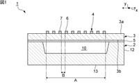
- FIG. 1 is a front sectional view of an elastic wave device according to a first embodiment of the present invention.
- FIG. 2 is a plan view of the elastic wave device according to the first embodiment of the present invention.
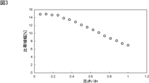
- FIG. 3 is a diagram showing the relationship between the ratio dh / dn and the specific bandwidth between the thickness of the heat dissipation film and the thickness of the lithium niobate film.
- FIG. 4A is a schematic front sectional view for explaining a ram wave propagating in a piezoelectric film of a conventional elastic wave device
- FIG. 4B is an elastic wave according to an embodiment of the present invention. It is a schematic front sectional view for demonstrating the bulk wave of the thickness slip mode propagating in a piezoelectric film in an apparatus.
- FIG. 1 is a front sectional view of an elastic wave device according to a first embodiment of the present invention.
- FIG. 2 is a plan view of the elastic wave device according to the first embodiment of the present invention.
- FIG. 3 is
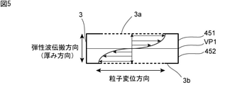
- FIG. 5 is a diagram showing the amplitude direction of the bulk wave in the thickness slip mode.
- FIG. 6 shows the relationship between dn / p and the specific band as a resonator when the distance between the centers of the adjacent first and second electrodes or the distance between the centers is p and the thickness of the piezoelectric film is dn. It is a figure which shows.
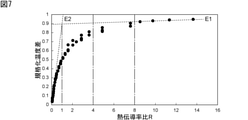
- FIG. 7 is a diagram showing the relationship between the thermal conductivity ratio and the normalized temperature difference.
- FIG. 8 is a front sectional view of an elastic wave device according to a modified example of the first embodiment of the present invention.
- FIG. 9 is a front sectional view of the elastic wave device according to the second embodiment of the present invention.
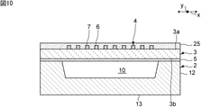
- FIG. 10 is a front sectional view of the elastic wave device according to the third embodiment of the present invention.
- FIG. 11 is a front sectional view of the elastic wave device according to the fourth embodiment of the present invention.
- FIG. 12 is a front sectional view of the elastic wave device according to the fifth embodiment of the present invention.
- FIG. 13 is a diagram showing a map of the specific band with respect to Euler angles (0 °, ⁇ , ⁇ ) of LiNbO 3 when dn / p is brought as close to 0 as possible.
- FIG. 1 is a front sectional view of an elastic wave device according to a first embodiment of the present invention.
- FIG. 2 is a plan view of the elastic wave device according to the first embodiment. Note that FIG. 1 is a cross-sectional view taken along the line I-I in FIG.
- the elastic wave device 1 has a support substrate 2, a lithium niobate film 3 as a piezoelectric film, a functional electrode 4, and a heat dissipation film 5.
- the piezoelectric film of the present invention is the lithium niobate film 3, but the piezoelectric film may be a lithium tantalate film.
- a lithium niobate film 3 is provided on the support substrate 2.
- the heat radiating film 5 is provided between the support substrate 2 and the lithium niobate film 3.
- a functional electrode 4 is provided on the lithium niobate film 3.
- the support substrate 2 has a cavity 10, a support 12, and a bottom 13.
- the support portion 12 has a frame-like shape.
- the cavity 10 is a recess provided in the support substrate 2.
- the cavity 10 is surrounded by a support 12 and a bottom 13 and is open on the lithium niobate film 3 side.
- the cavity 10 may be a through hole.
- the support substrate 2 is a silicon substrate.
- the plane orientation of the support substrate 2 on the surface of the lithium niobate film 3 side is preferably (100), (111) or (110).
- the resistivity of the support substrate 2 is preferably 2 k ⁇ or more.
- the material of the support substrate 2 is not limited to the above. As the material of the support substrate 2, it is preferable to use a material having high thermal conductivity.
- a lithium niobate film 3 is provided on the support portion 12 of the support substrate 2 so as to cover the cavity portion 10.
- the lithium niobate film 3 has a first main surface 3a and a second main surface 3b.
- the first main surface 3a and the second main surface 3b face each other.
- the second main surface 3b is the main surface on the support substrate 2 side.
- the lithium niobate film 3 is a LiNbO 3 film.
- the thickness of the lithium niobate film 3 is preferably 40 nm or more and 1000 nm or less.
- a heat radiating film 5 is provided on the second main surface 3b of the lithium niobate film 3.
- the heat radiating film 5 is provided so as to cover the cavity 10 of the support substrate 2. Therefore, the heat radiating film 5 is provided so as to bridge the support portion 12 of the support substrate 2.
- the thickness of the heat radiating film 5 is thinner than the thickness of the lithium niobate film 3.
- the thermal conductivity of the heat radiating film 5 is higher than that of the lithium niobate film 3.
- the heat radiating film 5 is made of a semiconductor or an insulator. More specifically, as the material of the heat radiating film 5, for example, silicon, aluminum nitride, silicon carbide, diamond, boron nitride, nanocarbon, or the like can be used.
- the heat radiating film 5 may overlap with at least a part of the support portion 12 of the support substrate 2 in a plan view.
- the plan view means the direction seen from above in FIG.
- the functional electrode 4 is provided on the first main surface 3a of the lithium niobate film 3.
- the functional electrode 4 has a plurality of electrodes.
- the plurality of electrodes are arranged in a direction intersecting with each other in the thickness direction of the lithium niobate film 3.
- Each electrode has a rectangular shape.
- the plurality of electrodes include a plurality of pairs of the first electrode 6 and the second electrode 7.
- the first electrode 6 and the second electrode 7 extend in parallel. Adjacent first electrodes 6 and second electrodes 7 face each other in a direction orthogonal to the direction in which the first electrode 6 extends.
- the direction in which the first electrode 6 extends is defined as the y direction
- the direction orthogonal to the y direction is defined as the x direction.
- Both the x-direction and the y-direction are directions that intersect with the thickness direction of the lithium niobate film 3. Therefore, it can be said that the adjacent first electrode 6 and the second electrode 7 face each other in the direction of crossing in the thickness direction of the lithium niobate film 3.
- the functional electrode 4 has a first bus bar 8 and a second bus bar 9.
- the first bus bar 8 and the second bus bar 9 face each other.
- One end of each of the plurality of first electrodes 6 is connected to the first bus bar 8.
- One end of each of the plurality of second electrodes 7 is connected to the second bus bar 9.
- the plurality of first electrodes 6 and the plurality of second electrodes 7 are interleaved with each other.
- the first electrode 6 and the second electrode 7 are connected to different potentials from each other.
- the functional electrode 4 is an IDT electrode.
- the functional electrode 4 is not limited to the IDT electrode.
- the functional electrode 4 may have at least a pair of the first electrode 6 and the second electrode 7.
- the functional electrode 4 is made of an appropriate metal or alloy such as Al or AlCu alloy.
- the Cu in the AlCu alloy is preferably 1% by weight or more and 20% by weight or less.
- the functional electrode 4 may be made of a laminated metal film. In this case, for example, it may have an adhesion layer. Examples of the adhesion layer include a Ti layer and a Cr layer.
- the functional electrode 4 has a crossover region A.
- the crossover region A is a region where adjacent electrodes overlap when viewed from the x direction.
- the crossover region A is a region in the x direction from one of the outermost electrodes of the functional electrode 4 to the other of the outermost electrodes.
- the crossover region A includes the outer end portion of the outermost electrode in the x direction. In a plan view, the entire crossover region A overlaps with the cavity 10.
- the feature of this embodiment is that it has the following configuration. 1) When the thickness of the piezoelectric film is dx and the distance between the centers of the adjacent first electrode 6 and the second electrode 7 is p, dx / p is 0.5 or less. 2) In a plan view, the heat radiation film 5 overlaps with at least a part of the support portion 12 of the support substrate 2. 3) The thermal conductivity of the heat radiating film 5 is higher than the thermal conductivity of the lithium niobate film 3, and the thickness of the heat radiating film 5 is thinner than the thickness of the lithium niobate film 3. Thereby, when the cavity 10 is provided in the support substrate 2, the heat dissipation of the elastic wave device 1 can be improved. This will be described below.
- the size of the elastic wave device 1 can be reduced.
- the miniaturization will be described later.
- the elastic wave device 1 is made smaller, the surface area becomes smaller, so that the heat dissipation property becomes lower.
- the support substrate 2 is provided with the cavity 10, it is difficult to dissipate the heat generated in the portion where the functional electrode 4 is provided.
- the heat radiating film 5 since the heat radiating film 5 is provided, the heat generated in the portion where the functional electrode 4 is provided can be conducted to the heat radiating film 5. Further, in a plan view, the heat radiation film 5 overlaps with at least a part of the support portion 12 of the support substrate 2, so that the distance between the heat radiation film 5 and the support substrate 2 is short. Therefore, heat can be efficiently conducted from the heat radiating film 5 to the support substrate 2. Therefore, when the cavity 10 is provided in the support substrate 2, the heat dissipation of the elastic wave device 1 can be improved. Further, since the thickness of the heat radiating film 5 is thinner than the thickness of the lithium niobate film 3, productivity can be improved.
- heat dissipation can be improved by increasing the size of the IDT electrode.
- the IDT electrode is made large, migration is likely to occur in the electrode finger. Therefore, the power resistance may deteriorate.
- the heat dissipation can be improved without making the functional electrode 4 large. Therefore, the heat dissipation can be improved without causing deterioration of the power resistance.
- the heat radiating film 5 is provided on the second main surface 3b of the lithium niobate film 3 and is in contact with the support substrate 2 as in the present embodiment. Thereby, heat can be further conducted from the heat radiating film 5 to the support substrate 2. It is more preferable that the heat radiating film 5 is provided so as to bridge at least a part of the support portion 12 of the support substrate 2. Thereby, the heat dissipation path can be further increased. In a plan view, it is more preferable that the heat radiating film 5 overlaps all of the cavities 10. In this case, the heat radiating film 5 is provided so as to bridge the entire support portion 12. Therefore, the number of heat dissipation paths can be further increased.
- thermal conductivity of each of the examples of materials that can be used for the heat radiating film 5 is shown in Table 1.
- the thermal conductivity of LiNbO 3 is 4.6 W / mK.
- the thermal conductivity of LiTaO3 is 4.2 W / mK.
- the heat radiation film 5 is preferably a silicon film, a silicon nitride film, or a silicon carbide film. More specifically, the heat radiating film 5 is preferably a Si film, an AlN film or a SiC film. In these cases, heat dissipation can be improved and the cost can be reduced.
- the thermal conductivity of the heat radiating film 5 is preferably 5 times or more the thermal conductivity of the lithium niobate film 3. Thereby, the heat dissipation property can be effectively improved.
- the thermal conductivity of the heat radiating film 5 can be significantly increased, and the heat radiating property can be further improved. This also applies when the piezoelectric film is a lithium tantalate film.
- the thickness of the heat radiating film 5 is dh
- the thickness of the lithium niobate film 3 is dn
- the ratio of the thickness dh of the heat radiating film 5 to the thickness dn of the lithium niobate film 3 is dh / dn.
- FIG. 3 shows the relationship between the ratio dh / dn and the specific bandwidth. A wide specific bandwidth indicates a high coupling coefficient.
- FIG. 3 is a diagram showing the relationship between the ratio dh / dn and the specific bandwidth between the thickness of the heat dissipation film and the thickness of the lithium niobate film.
- the ratio dh / dn is preferably 0.25 or less. That is, the thickness of the heat radiating film 5 is preferably 25% or less of that of the lithium niobate film 3. More specifically, the thickness of the thickest portion of the heat radiating film 5 is preferably 25% or less of that of the lithium niobate film 3. Thereby, the specific bandwidth can be further increased and the coupling coefficient can be further increased. On the other hand, the thickness of the heat radiating film 5 is preferably 5% or more of that of the lithium niobate film 3. In this case, the heat dissipation property can be suitably improved. The thickness of the heat radiating film 5 is more preferably 50% or more of that of the lithium niobate film 3. In this case, the heat dissipation can be further improved. In the following, the specific bandwidth may be referred to as the specific band.
- the reflector is not provided on the lithium niobate film 3.
- the elastic wave device 1 does not have a reflector.
- the propagation loss is suppressed because the elastic wave device 1 uses the bulk wave in the thickness slip mode. More specifically, the elastic wave device 1 utilizes a bulk wave in the thickness slip primary mode.
- the details of the thickness slip mode used by the elastic wave device 1 will be described.
- a plurality of pairs of adjacent first electrode 6 and second electrode 7 structures are provided in the x direction.
- This logarithm does not have to be an integer pair, and may be 1.5 pairs, 2.5 pairs, or the like.
- the case where the electrodes in the functional electrodes 4 are adjacent to each other does not mean the case where the electrodes are arranged so as to be in direct contact with each other, but the case where the electrodes are arranged so as to be spaced apart from each other.
- no other hot electrode or ground electrode is arranged between the first electrode 6 and the second electrode 7.
- an AC voltage is applied between the plurality of first electrodes 6 and the plurality of second electrodes 7. More specifically, an AC voltage is applied between the first bus bar 8 and the second bus bar 9. As a result, it is possible to obtain resonance characteristics using the bulk wave in the thickness slip mode excited by the lithium niobate film 3.
- the region between the first electrode 6 and the second electrode 7 is the excitation region B.
- one excitation region B is shown as an example, but the region between the plurality of first electrodes 6 and the plurality of second electrodes 7 is the excitation region B.
- the excitation region B is included in the crossover region A.
- the heat radiation film 5 preferably overlaps with the crossover region A, and more preferably overlaps with the excitation region B.
- heat is generated in the excitation region B in the crossover region A. Therefore, with the above configuration, heat can be efficiently conducted to the heat radiating film 5 from the heat-generating portion. Therefore, the heat dissipation property can be further improved.
- dx / p is set to 0.5 or less as described above. More specifically, the thickness of the lithium niobate film 3 is dn, and the distance between the centers of the adjacent first electrode 6 and the second electrode 7 of the plurality of pairs of the first electrode 6 and the second electrode 7 is p. , Dn / p is 0.5 or less. Therefore, the bulk wave in the thickness slip mode is effectively excited, and good resonance characteristics can be obtained.
- the distance between the centers of the first electrode 6 and the second electrode 7 is the distance connecting the center of the first electrode 6 in the x direction and the center of the second electrode 7 in the x direction.
- the elastic wave device 1 has the above configuration and uses the thickness slip mode. As a result, even if the logarithm of the first electrode 6 and the second electrode 7 is reduced, the Q value is unlikely to decrease.
- the lithium niobate film 3 is a Z-cut piezoelectric film. Therefore, the x direction is a direction orthogonal to the polarization direction of the lithium niobate film 3. This does not apply when the lithium niobate film 3 is a piezoelectric film having another cut angle.
- FIG. 4A is a schematic front sectional view for explaining a Lamb wave propagating in a piezoelectric film of an elastic wave device as described in Patent Document 1.
- the wave propagates in the piezoelectric film 201 as shown by an arrow.
- the first main surface 201a and the second main surface 201b face each other, and the thickness direction connecting the first main surface 201a and the second main surface 201b is the z direction.
- the x direction is the direction in which the electrode fingers of the IDT electrodes are lined up.
- the Lamb wave propagates in the x direction. Since the Lamb wave is a plate wave, the piezoelectric film 201 vibrates as a whole, but the wave propagates in the x direction. Therefore, reflectors are arranged on both sides of the IDT electrode in the x direction to obtain resonance characteristics.
- the vibration displacement is in the thickness slip direction. Therefore, the wave propagates almost in the z direction and resonates. Therefore, the x-direction component of the wave is significantly smaller than the z-direction component. Since the resonance characteristic is obtained by the propagation of the wave in the z direction, the propagation loss is unlikely to occur even if the number of electrode fingers of the reflector is reduced. Further, even if the logarithm of the electrode pair composed of the first electrode 6 and the second electrode 7 is reduced in order to promote miniaturization, the Q value is unlikely to decrease.
- FIG. 5 schematically shows a bulk wave when a voltage at which the second electrode 7 has a higher potential than that of the first electrode 6 is applied between the first electrode 6 and the second electrode 7.
- the first region 451 is a region of the excitation region between the virtual plane VP1 orthogonal to the thickness direction of the lithium niobate film 3 and dividing the lithium niobate film 3 into two, and the first main surface 3a.
- the second region 452 is a region of the excitation region between the virtual plane VP1 and the second main surface 3b.
- the elastic wave device 1 a plurality of pairs of the first electrode 6 and the second electrode 7 are arranged. Since the thickness slip mode does not propagate the wave in the x direction, it is not necessary to provide a plurality of pairs of electrodes including the first electrode 6 and the second electrode 7. That is, at least a pair of the first electrode 6 and the second electrode 7 need be provided.
- the first electrode 6 is an electrode connected to a hot potential
- the second electrode 7 is an electrode connected to a ground potential.
- the first electrode 6 may be connected to the ground potential and the second electrode 7 may be connected to the hot potential.
- at least one pair of electrodes is an electrode connected to a hot potential or an electrode connected to a ground potential as described above, and is not provided with a floating electrode.
- dn / p is 0.5 or less.
- the dn / p is preferably 0.24 or less. In that case, even better resonance characteristics can be obtained. This will be described with reference to FIG.
- FIG. 6 is a diagram showing the relationship between this dn / p and the specific band as a resonator of the elastic wave device.
- the ratio band is less than 5% even if dn / p is adjusted.
- the ratio band can be set to 5% or more by changing dn / p within that range. Therefore, it is possible to construct a resonator having a high coupling coefficient.
- the specific band can be increased to 7% or more.
- a resonator having a wider specific band can be obtained, and a resonator having a higher coupling coefficient can be realized.
- a value obtained by averaging the thickness may be adopted.
- the distance p between the centers of the adjacent first electrode 6 and the second electrode 7 is preferably 1 ⁇ m or more and 10 ⁇ m or less.
- the widths of the first electrode 6 and the second electrode 7 are preferably 150 nm or more and 1000 nm or less, respectively.
- w the average width of the first electrode and the second electrode
- De the duty ratio of the functional electrode
- Ce the thermal conductivity of the functional electrode
- the thermal conductivity of the lithium niobate film is Cn
- the thickness of the lithium niobate film is dn
- the thermal conductivity of the heat dissipation film is Ci
- the thickness of the heat dissipation film is di.
- R (Ce ⁇ de ⁇ De) / (Cn ⁇ dn + Ci ⁇ di).
- the normalized temperature difference is used as an index of heat dissipation.
- the normalized temperature difference is a standardized difference between the temperature when the elastic wave is not excited and the temperature when the elastic wave is excited in the elastic wave device. When the elastic wave is excited, heat is generated in the portion where the functional electrode is provided, and the temperature of the elastic wave device becomes high.
- the higher the heat dissipation of the elastic wave device the more heat is dissipated. Therefore, the higher the heat dissipation, the smaller the difference between the temperature when the elastic wave is not excited and the temperature when the elastic wave is excited. Therefore, the smaller the normalized temperature difference, the higher the heat dissipation of the elastic wave device.
- FIG. 7 is a diagram showing the relationship between the thermal conductivity ratio and the normalized temperature difference.
- the broken line E1 and the broken line E2 in FIG. 7 indicate the slope of the change in the normalized temperature difference with respect to the change in the thermal conductivity ratio R.
- R ⁇ 8 is preferable, R ⁇ 4 is more preferable, and R ⁇ 1 is even more preferable. As a result, the normalized temperature difference can be effectively reduced, and the heat dissipation can be effectively improved.
- the heat radiating film 5 may overlap with at least a part of the support portion 12 in the support substrate 2 in a plan view.
- a modified example of the first embodiment in which only the arrangement of the heat radiating film is different from that of the first embodiment, will be shown.
- the heat radiating film 5A overlaps a part of the support portion 12 in the support substrate 2 in a plan view. More specifically, in the cross section shown in FIG. 8, one of the facing portions of the support portion 12 overlaps with the heat radiating film 5A in a plan view. The other portion of the facing portions of the support portion 12 does not overlap with the heat radiating film 5A in a plan view. The portion of the support portion 12 that does not overlap with the heat dissipation film 5A is in direct contact with the lithium niobate film 3.
- the heat radiation film 5A also overlaps with the crossover region A of the functional electrode 4 in a plan view. Also in this modification, the heat dissipation can be improved as in the first embodiment.
- FIG. 9 is a front sectional view of the elastic wave device according to the second embodiment.
- This embodiment is different from the first embodiment in that the heat radiating film 25 is provided on the first main surface 3a of the lithium niobate film 3.
- the heat radiating film 5 is not provided on the second main surface 3b.
- the elastic wave device of the present embodiment has the same configuration as the elastic wave device 1 of the first embodiment.
- the heat radiating film 25 is provided on the first main surface 3a of the lithium niobate film 3 so as to cover the functional electrode 4. Also in this embodiment, the thickness of the heat radiating film 25 is thinner than the thickness of the lithium niobate film 3. In a plan view, the heat dissipation film 25 overlaps with the support portion 12 of the support substrate 2.
- the thermal conductivity of the lithium niobate film 3 is low. Therefore, it is difficult to improve the efficiency of heat transfer from the portion of the lithium niobate film 3 where the functional electrode 4 is provided to the portion in contact with the support portion 12.
- heat can be efficiently transferred to the portion overlapping the support portion 12 in a plan view via the heat radiating film 25. Therefore, heat dissipation can be improved.
- the heat radiating film 25 is provided on the first main surface 3a of the lithium niobate film 3, it is preferable that the heat radiating film 25 overlaps all of the cavities 10 in a plan view. Thereby, the heat dissipation path can be increased. Therefore, the heat dissipation property can be effectively improved.
- FIG. 10 is a front sectional view of the elastic wave device according to the third embodiment.
- the first embodiment of the present embodiment is in that the heat radiating film 25 is provided on the first main surface 3a of the lithium niobate film 3 and the heat radiating film 5 is provided on the second main surface 3b. Different from the form. Except for the above points, the elastic wave device of the third embodiment has the same configuration as the elastic wave device 1 of the first embodiment.
- heat can be efficiently transferred to the support substrate 2 via the heat radiating film 5 and the heat radiating film 25 as in the first embodiment and the second embodiment. Therefore, heat dissipation can be improved.
- FIG. 11 is a front sectional view of the elastic wave device according to the fourth embodiment.
- This embodiment is different from the first embodiment in that the heat radiating film 35 and the support substrate 32 are integrally provided, and the shape of the cavity 30 is different from that of the first embodiment. Except for the above points, the elastic wave device 31 of the fourth embodiment has the same configuration as the elastic wave device 1 of the first embodiment.
- the material of the heat radiating film 35 and the material of the support substrate 32 are the same.
- the heat radiating film 35 bridges the support portion 12 of the support substrate 32.
- the heat radiating film 35 bridges the entire support portion 12.
- the heat radiating film 35 and the support portion 12 are flush with each other on the lithium niobate film 3 side.
- the heat radiating film 35 and the support portion 12 are in contact with the second main surface 3b of the lithium niobate film 3.
- the cavity 30 of the support substrate 32 is a recess provided in the support substrate 32. More specifically, the cavity 30 is a recess surrounded by the support 12 and the heat radiation film 35.
- the support substrate 32 of this embodiment does not have a bottom 13 as in the first embodiment.
- the cavity 30 is a recess that is open on the side facing the heat radiating film 35.
- the heat radiating film 35 and the support substrate 32 are integrated. Thereby, heat can be efficiently radiated to the outside of the elastic wave device 31 via the heat radiating film 35 and the support substrate 32. Therefore, the heat dissipation property can be further improved.
- the heat radiating film 35 and the support substrate 32 are obtained, for example, by etching the base material of the support substrate 32.
- the portion other than the portion forming the heat radiating film 35 may be masked with a resist film or the like and then etched.
- the etching rate of the portion of the base material that forms the heat dissipation film 35 and the etching rate of the other portion may be different.
- the base material may be appropriately doped. It may be etched after that.
- the compositions of the heat radiating film 35 and the support portion 12 of the support substrate 32 are different. However, even in this case, the composition of the heat radiating film 35 and the support portion 12 is the same except for the doped component.
- the heat radiating film 35 does not necessarily have to crosslink the support portion 12.
- the heat radiating film 35 may be provided integrally with at least a part of the support portion 12. Even in this case, the heat dissipation can be improved. However, it is preferable that the heat radiating film 35 crosslinks at least a part of the support portion 12, and more preferably all of the support portion 12 is crosslinked. Thereby, the heat dissipation property can be further improved.
- FIG. 12 is a front sectional view of the elastic wave device according to the fifth embodiment.
- the configuration of the heat radiating film 45 is different from that of the first embodiment.
- the elastic wave device of the present embodiment has the same configuration as the elastic wave device 1 of the first embodiment.
- the heat radiating film 45 has a first portion 45a and a second portion 45b.
- the first portion 45a is a portion that overlaps with the first electrode 6 or the second electrode 7 in a plan view.
- the second portion 45b is a portion that overlaps the portion between the first electrode 6 and the second electrode 7 in a plan view.
- the second portion 45b does not overlap with the first electrode and the second electrode 7 in a plan view.
- the thickness of the second portion 45b is thicker than the thickness of the first portion 45a.
- the thickness of at least a part of the second portion 45b may be thicker than the thickness of the first portion 45a.
- the center in the x direction between the center of the first electrode 6 in the x direction and the center of the second electrode 7 in the x direction is defined as the interfinger center portion O. It is preferable that the thickness of the portion of the second portion 45b including the portion overlapping the central portion O between the electrodes in a plan view is thicker than the thickness of the first portion 45a. In the lithium niobate film 3, the portion located at the central portion O between the electrodes of the electrodes generates heat particularly. By increasing the thickness of the portion of the heat radiating film 45, the heat radiating property can be further effectively improved.
- the following shows examples of preferred Euler angles ( ⁇ , ⁇ , ⁇ ) of the lithium niobate film 3.
- FIG. 13 is a diagram showing a map of the specific band with respect to Euler angles (0 °, ⁇ , ⁇ ) of LiNbO 3 when dn / p is brought as close to 0 as possible.
- the portion shown with hatching in FIG. 13 is a region where a specific band of at least 5% or more can be obtained, and when the range of the region is approximated, the following equations (1), (2) and (3) are approximated. ).
- Equation (1) (0 ° ⁇ 10 °, 20 ° ⁇ 80 °, 0 ° ⁇ 60 ° (1- ( ⁇ -50) 2/900) 1/2) or (0 ° ⁇ 10 °, 20 ° ⁇ 80 °, [180 ° -60 ° (1- ( ⁇ - 50) 2/900) 1/2] ⁇ 180 °) ... equation (2) (0 ° ⁇ 10 °, [ 180 ° -30 ° (1- ( ⁇ -90) 2/8100) 1/2] ⁇ 180 °, any [psi) ... Equation (3)
- the thickness of the heat radiating film is preferably 25% or less of that of the lithium tantalate film. Thereby, the specific bandwidth can be further increased and the coupling coefficient can be further increased.
- the thickness of the heat radiating film is preferably 5% or more, more preferably 50% or more of the lithium tantalate film. In this case, the heat dissipation can be further improved.
- the relationship shown in FIG. 7 is similarly established even when the piezoelectric film is a lithium tantalate film.
- the thermal conductivity of the piezoelectric film is Cx
- the thickness of the piezoelectric film is dx.
- Rx ⁇ 8 is preferable, Rx ⁇ 4 is more preferable, and Rx ⁇ 1 is even more preferable.
- the standardized temperature difference can be effectively reduced, and the heat dissipation property can be effectively improved.
Landscapes
- Physics & Mathematics (AREA)
- Acoustics & Sound (AREA)
- Surface Acoustic Wave Elements And Circuit Networks Thereof (AREA)
Abstract
支持基板に空洞部が設けられている場合において、放熱性を高めることができる、弾性波装置を提供する。 本発明に係る弾性波装置1は、空洞部10と、支持部12とを有する支持基板2と、支持部12上に設けられており、かつ第1,第2の主面3a,3bを有する圧電膜(ニオブ酸リチウム膜3)と、第1の主面3aに設けられている機能電極4と、圧電膜の第1,第2の主面3a,3bのうち少なくとも一方に設けられており、半導体または絶縁体からなる放熱膜5とを備える。機能電極4は、少なくとも1対の第1,第2電極6,7を有する。圧電膜の厚みをdx、隣り合う第1,第2電極6,7の中心間距離をpとした場合、dx/pが0.5以下である。平面視において、放熱膜5が支持部12の少なくとも一部と重なっている。放熱膜5の熱伝導率が圧電膜の熱伝導率よりも高く、かつ放熱膜5の厚みが圧電膜の厚みよりも薄い。
Description
本発明は、弾性波装置に関する。
従来、LiNbO3またはLiTaO3からなる圧電膜を伝搬する板波を利用した弾性波装置が知られている。例えば、下記の特許文献1では、板波としてのラム波を利用した弾性波装置が開示されている。ここでは、支持体上に圧電基板が設けられている。支持体、すなわち支持基板には空洞部が設けられている。圧電基板は空洞部と重なっている。圧電基板はLiNbO3またはLiTaO3からなる。圧電基板の上面にIDT電極が設けられている。IDT電極の一方電位に接続される複数の電極指と、他方電位に接続される複数の電極指との間に電圧が印加される。それによって、ラム波が励振される。このIDT電極の両側には反射器が設けられている。それによって、板波を利用した弾性波共振子が構成されている。
特許文献1に記載の弾性波装置では、圧電基板が空洞部に面している部分においては、放熱性が低い。そのため、弾性波装置全体としても放熱性が低い。ここで、IDT電極に電力を加えると、IDT電極が設けられている部分において発熱する。上記弾性波装置のように放熱性が低い場合には、IDT電極が設けられている部分における発熱に起因して、弾性波装置が破損するおそれがある。そのため、放熱性が低い弾性波装置においては、耐電力性を高めることは困難である。
本発明の目的は、支持基板に空洞部が設けられている場合において、放熱性を高めることができる、弾性波装置を提供することにある。
本発明に係る弾性波装置のある広い局面では、空洞部と、支持部とを有する支持基板と、前記空洞部を覆うように、前記支持部上に設けられており、かつ対向し合う第1の主面及び第2の主面を有する圧電膜と、前記圧電膜の前記第1の主面に設けられている機能電極と、前記圧電膜の前記第1の主面及び前記第2の主面のうち少なくとも一方に設けられており、半導体または絶縁体からなる放熱膜とが備えられており、前記機能電極が、互いに対向する、少なくとも1対の第1電極及び第2電極を有し、前記圧電膜の厚みをdx、隣り合う前記第1電極と前記第2電極との中心間距離をpとした場合、dx/pが0.5以下であり、平面視において、前記放熱膜が前記支持部の少なくとも一部と重なっており、前記放熱膜の熱伝導率が前記圧電膜の熱伝導率よりも高く、かつ前記放熱膜の厚みが前記圧電膜の厚みよりも薄い。
本発明に係る弾性波装置の他の広い局面では、空洞部と、支持部とを有する支持基板と、前記空洞部を覆うように、前記支持部上に設けられており、かつ対向し合う第1の主面及び第2の主面を有する圧電膜と、前記圧電膜の前記第1の主面に設けられている機能電極と、前記圧電膜の前記第1の主面及び前記第2の主面のうち少なくとも一方に設けられている放熱膜とが備えられており、前記機能電極が、互いに対向する、少なくとも1対の第1電極及び第2電極を有し、前記圧電膜の厚みをdx、隣り合う前記第1電極と前記第2電極との中心間距離をpとした場合、dx/pが0.5以下であり、平面視において、前記放熱膜が前記支持部の少なくとも一部と重なっており、前記放熱膜の厚みが前記圧電膜の厚みよりも薄く、前記放熱膜が、シリコン膜、窒化ケイ素膜または炭化ケイ素膜である。
本発明に係る弾性波装置によれば、支持基板に空洞部が設けられている場合において、放熱性を高めることができる。
以下、図面を参照しつつ、本発明の具体的な実施形態を説明することにより、本発明を明らかにする。
なお、本明細書に記載の各実施形態は、例示的なものであり、異なる実施形態間において、構成の部分的な置換または組み合わせが可能であることを指摘しておく。
図1は、本発明の第1の実施形態に係る弾性波装置の正面断面図である。図2は第1の実施形態に係る弾性波装置の平面図である。なお、図1は、図2中のI-I線に沿う断面図である。
図1に示すように、弾性波装置1は支持基板2、圧電膜としてのニオブ酸リチウム膜3、機能電極4及び放熱膜5を有する。弾性波装置1においては、本発明の圧電膜はニオブ酸リチウム膜3であるが、圧電膜はタンタル酸リチウム膜であってもよい。支持基板2上にニオブ酸リチウム膜3が設けられている。なお、本実施形態においては、支持基板2とニオブ酸リチウム膜3との間に放熱膜5が設けられている。ニオブ酸リチウム膜3上に機能電極4が設けられている。
支持基板2は空洞部10、支持部12及び底部13を有する。支持部12は枠状の形状を有する。空洞部10は、支持基板2に設けられた凹部である。空洞部10は、支持部12及び底部13により囲まれており、ニオブ酸リチウム膜3側において開口している。なお、空洞部10は、貫通孔であってもよい。
支持基板2はシリコン基板である。支持基板2のニオブ酸リチウム膜3側の面における面方位は(100)、(111)または(110)であることが好ましい。支持基板2の抵抗率は2kΩ以上であることが好ましい。もっとも、支持基板2の材料は上記に限定されない。支持基板2の材料には、熱伝導率が高い材料を用いることが好ましい。
支持基板2の支持部12上に、空洞部10を覆うように、ニオブ酸リチウム膜3が設けられている。ニオブ酸リチウム膜3は第1の主面3a及び第2の主面3bを有する。第1の主面3a及び第2の主面3bは対向し合っている。第1の主面3a及び第2の主面3bのうち、第2の主面3bが支持基板2側の主面である。本実施形態では、ニオブ酸リチウム膜3はLiNbO3膜である。ニオブ酸リチウム膜3の厚みは40nm以上、1000nm以下であることが好ましい。
ニオブ酸リチウム膜3の第2の主面3bに放熱膜5が設けられている。放熱膜5は、支持基板2の空洞部10を覆うように設けられている。よって、放熱膜5は、支持基板2の支持部12を架橋するように設けられている。放熱膜5の厚みはニオブ酸リチウム膜3の厚みよりも薄い。放熱膜5の熱伝導率はニオブ酸リチウム膜3の熱伝導率よりも高い。放熱膜5は半導体または絶縁体からなる。より具体的には、放熱膜5の材料としては、例えば、シリコン、窒化アルミニウム、炭化ケイ素、ダイヤモンド、窒化ホウ素またはナノカーボンなどを用いることができる。
なお、放熱膜5は、平面視において、支持基板2の支持部12の少なくとも一部と重なっていればよい。本明細書において、平面視とは、図1における上方から見る方向をいう。
図2に示すように、ニオブ酸リチウム膜3の第1の主面3aに機能電極4が設けられている。機能電極4は複数の電極を有する。複数の電極は、ニオブ酸リチウム膜3の厚み方向に交叉する方向に並んでいる。各電極は矩形形状を有する。複数の電極は、複数対の第1電極6及び第2電極7を含む。本実施形態においては、第1電極6及び第2電極7は平行に延びている。第1電極6が延びる方向と直交する方向において、隣り合う第1電極6及び第2電極7が対向している。以下においては、第1電極6が延びる方向をy方向とし、y方向と直交する方向をx方向とする。x方向及びy方向の双方は、ニオブ酸リチウム膜3の厚み方向と交叉する方向である。このため、隣り合う第1電極6及び第2電極7は、ニオブ酸リチウム膜3の厚み方向に交叉する方向において対向しているともいえる。
機能電極4は第1のバスバー8及び第2のバスバー9を有する。第1のバスバー8及び第2のバスバー9は対向し合っている。複数の第1電極6の一方端が、それぞれ第1のバスバー8に接続されている。複数の第2電極7の一方端が、それぞれ第2のバスバー9に接続されている。複数の第1電極6及び複数の第2電極7は、互いに間挿し合っている。第1電極6及び第2電極7は、互いに異なる電位に接続される。本実施形態においては、機能電極4はIDT電極である。もっとも、機能電極4はIDT電極には限られない。機能電極4は、少なくとも一対の第1電極6及び第2電極7を有していればよい。
機能電極4は、Al、AlCu合金などの適宜の金属もしくは合金からなる。AlCu合金におけるCuは、1重量%以上、20重量%以下であることが好ましい。機能電極4は、積層金属膜からなっていてもよい。この場合、例えば、密着層を有していてもよい。密着層としては、例えば、Ti層やCr層などが挙げられる。
図2に示すように、機能電極4は交叉領域Aを有する。交叉領域Aは、x方向から見て、隣り合う電極が重なっている領域である。交叉領域Aは、x方向における、機能電極4の最も外側の電極のうちの一方の電極から、最も外側の電極のうちの他方の電極に至る領域である。なお、交叉領域Aは、上記最も外側の電極の、x方向における外側の端部を含む。平面視において、交叉領域Aの全部が空洞部10と重なっている。
本実施形態の特徴は、以下の構成を有することにある。1)圧電膜の厚みをdx、隣り合う第1電極6と第2電極7との中心間距離をpとした場合、dx/pが0.5以下であること。2)平面視において、放熱膜5が支持基板2の支持部12の少なくとも一部と重なっていること。3)放熱膜5の熱伝導率がニオブ酸リチウム膜3の熱伝導率よりも高く、かつ放熱膜5の厚みがニオブ酸リチウム膜3の厚みよりも薄いこと。それによって、支持基板2に空洞部10が設けられている場合において、弾性波装置1の放熱性を高めることができる。これを以下において説明する。
厚み滑りモードのバルク波を利用していることにより、弾性波装置1の小型化を進めることができる。なお、該小型化については後述する。しかしながら、弾性波装置1を小型にすると、表面積が小さくなるため、放熱性が低くなる。加えて、支持基板2に空洞部10が設けられていると、機能電極4が設けられた部分において生じた熱を放熱し難い。
これに対して、本実施形態においては、放熱膜5が設けられていることにより、機能電極4が設けられた部分において生じた熱を、放熱膜5に伝導させることができる。さらに、平面視において、放熱膜5が支持基板2の支持部12の少なくとも一部と重なっていることにより、放熱膜5と支持基板2との距離が近い。よって、放熱膜5から支持基板2に、熱を効率的に伝導させることができる。従って、支持基板2に空洞部10が設けられている場合において、弾性波装置1の放熱性を高めることができる。さらに、放熱膜5の厚みがニオブ酸リチウム膜3の厚みよりも薄いため、生産性を高めることもできる。
なお、従来の板波を利用する素子においても、IDT電極を大型にすることにより、放熱性を高め得る。しかしながら、IDT電極を大型にすると、電極指においてマイグレーションが生じ易くなる。そのため、耐電力性が劣化するおそれがある。これに対して、本実施形態においては、機能電極4を大型にせずして、放熱性を高めることができる。よって、耐電力性の劣化を生じさせることなく、放熱性を高めることができる。
本実施形態のように、放熱膜5がニオブ酸リチウム膜3の第2の主面3bに設けられており、かつ支持基板2と接触していることが好ましい。それによって、放熱膜5から支持基板2に、熱をより一層伝導させることができる。放熱膜5が、支持基板2の支持部12の少なくとも一部を架橋するように設けられていることがより好ましい。それによって、放熱経路をより一層増やすことができる。平面視において、放熱膜5が空洞部10の全てと重なっていることがさらに好ましい。この場合には、放熱膜5が、支持部12の全部を架橋するように設けられている。よって、放熱経路をさらにより一層増やすことができる。
ここで、放熱膜5に用いられ得る材料の例の、それぞれの熱伝導率を表1において示す。なお、LiNbO3の熱伝導率は4.6W/mKである。LiTaO3の熱伝導率は4.2W/mKである。

表1に示す全ての材料の熱伝導率が、LiNbO3及びLiTaO3の熱伝導率よりも大幅に高いことがわかる。放熱膜5は、シリコン膜、窒化ケイ素膜または炭化ケイ素膜であることが好ましい。より具体的には、放熱膜5は、Si膜、AlN膜またはSiC膜であることが好ましい。これらの場合には、放熱性を高めることができ、かつコストを低くすることができる。
放熱膜5の熱伝導率は、ニオブ酸リチウム膜3の熱伝導率の5倍以上であることが好ましい。それによって、放熱性を効果的に高めることができる。もっとも、放熱膜5に、表1に示す材料を用いた場合には、放熱膜5の熱伝導率を大幅に高めることができ、放熱性をより一層高めることができる。これは、圧電膜がタンタル酸リチウム膜である場合も同様である。
ここで、放熱膜5の厚みをdh、ニオブ酸リチウム膜3の厚みをdn、放熱膜5の厚みdhとニオブ酸リチウム膜3の厚みdnとの比をdh/dnとする。図3において、比dh/dnと比帯域幅との関係を示す。比帯域幅が広いことは、結合係数が高いことを示す。
図3は、放熱膜の厚みとニオブ酸リチウム膜の厚みとの比dh/dn、及び比帯域幅の関係を示す図である。
図3に示すように、比dh/dnが小さくなるほど、比帯域幅が広くなっていることがわかる。比dh/dnは、0.25以下であることが好ましい。すなわち、放熱膜5の厚みは、ニオブ酸リチウム膜3の25%以下であることが好ましい。より具体的には、放熱膜5の最も厚い部分の厚みが、ニオブ酸リチウム膜3の25%以下であることが好ましい。それによって、比帯域幅をより一層広くすることができ、結合係数をより一層高めることができる。一方で、放熱膜5の厚みは、ニオブ酸リチウム膜3の5%以上であることが好ましい。この場合には、放熱性を好適に高めることができる。放熱膜5の厚みは、ニオブ酸リチウム膜3の50%以上であることがより好ましい。この場合には、放熱性をより一層高めることができる。なお、以下においては、比帯域幅を比帯域と記載することもある。
ところで、本実施形態においては、ニオブ酸リチウム膜3上に反射器は設けられていない。弾性波装置1は反射器を有しない。この場合にも伝搬損失が抑制されるのは、弾性波装置1が厚み滑りモードのバルク波を利用していることによる。より具体的には、弾性波装置1は厚み滑り1次モードのバルク波を利用している。以下において、弾性波装置1が利用している厚み滑りモードの詳細を説明する。
図2に示すように、隣り合う1対の第1電極6及び第2電極7の構造が、x方向に、複数対設けられている。この対数は、整数対である必要はなく、1.5対や2.5対などであってもよい。なお、機能電極4における電極が隣り合うとは、電極同士が直接接触するように配置されている場合ではなく、電極同士が間隔を介して配置されている場合を指す。また、第1電極6と第2電極7とが隣り合う場合、第1電極6と第2電極7との間には、他のホット電極またはグラウンド電極は配置されない。
弾性波装置1の駆動に際しては、複数の第1電極6と、複数の第2電極7との間に交流電圧を印加する。より具体的には、第1のバスバー8と第2のバスバー9との間に交流電圧を印加する。それによって、ニオブ酸リチウム膜3において励振される厚み滑りモードのバルク波を利用した、共振特性を得ることが可能とされている。このように、第1電極6と第2電極7との間の領域は励振領域Bである。図2においては、例として1つの励振領域Bを示しているが、複数の第1電極6と複数の第2電極7との間の領域は、いずれも励振領域Bである。励振領域Bは交叉領域Aに含まれる。
放熱膜5は、平面視において、交叉領域Aと重なっていることが好ましく、励振領域Bと重なっていることがより好ましい。弾性波装置1においては、交叉領域Aにおける励振領域Bにおいて発熱する。よって、上記構成により、発熱している部分から、熱を効率的に放熱膜5に伝導させることができる。従って、放熱性をより一層高めることができる。
弾性波装置1では、上記のように、dx/pは0.5以下とされている。より具体的には、ニオブ酸リチウム膜3の厚みをdn、複数対の第1電極6及び第2電極7のうちいずれかの隣り合う第1電極6及び第2電極7の中心間距離をpとした場合、dn/pは0.5以下とされている。そのため、上記厚み滑りモードのバルク波が効果的に励振され、良好な共振特性を得ることができる。ここで、第1電極6及び第2電極7の中心間距離とは、第1電極6のx方向における中心と、第2電極7のx方向における中心とを結んだ距離となる。
弾性波装置1は上記構成を備え、厚み滑りモードを利用している。それによって、第1電極6及び第2電極7の対数を少なくしたとしても、Q値の低下が生じ難い。
本実施形態では、ニオブ酸リチウム膜3はZカットの圧電膜である。そのため、x方向は、ニオブ酸リチウム膜3の分極方向と直交する方向となる。ニオブ酸リチウム膜3が他のカット角の圧電膜である場合には、この限りでない。
厚み滑りモードのバルク波と、従来利用されているラム波との相違を、図4(a)及び図4(b)を参照して説明する。
図4(a)は、特許文献1に記載のような弾性波装置の圧電膜を伝搬するラム波を説明するための模式的正面断面図である。ここでは、圧電膜201中を矢印で示すように波が伝搬する。ここで、圧電膜201では、第1の主面201aと、第2の主面201bとが対向しており、第1の主面201aと第2の主面201bとを結ぶ厚み方向がz方向である。x方向は、IDT電極の電極指が並んでいる方向である。図4(a)に示すように、ラム波はx方向に伝搬していく。ラム波は板波であるため、圧電膜201が全体として振動するものの、波はx方向に伝搬する。そのため、IDT電極のx方向両側に反射器を配置して、共振特性を得ている。
これに対して、図4(b)に示すように、本実施形態の弾性波装置では、振動変位は厚み滑り方向である。そのため、波はz方向にほぼ伝搬し、共振する。よって、波のx方向成分がz方向成分に比べて著しく小さい。そして、このz方向の波の伝搬により共振特性が得られるため、反射器の電極指の本数を少なくしても、伝搬損失は生じ難い。さらに、小型化を進めようとして、第1電極6及び第2電極7からなる電極対の対数を減らしたとしても、Q値の低下が生じ難い。
なお、厚み滑りモードのバルク波の振幅方向は、図5に示すように、ニオブ酸リチウム膜3の励振領域に含まれる第1領域451と、励振領域に含まれる第2領域452とにおいて逆になる。図5では、第1電極6と第2電極7との間に、第2電極7が第1電極6よりも高電位となる電圧が印加された場合のバルク波を模式的に示してある。第1領域451は、励振領域のうち、ニオブ酸リチウム膜3の厚み方向に直交しニオブ酸リチウム膜3を2分する仮想平面VP1と、第1の主面3aとの間の領域である。第2領域452は、励振領域のうち、仮想平面VP1と、第2の主面3bとの間の領域である。
上記のように、弾性波装置1では、複数対の第1電極6及び第2電極7が配置されている。厚み滑りモードは、x方向に波を伝搬させるものではないため、第1電極6及び第2電極7からなる電極対は複数対設けられている必要はない。すなわち、少なくとも1対の第1電極6及び第2電極7が設けられてさえおればよい。
弾性波装置1においては、第1電極6がホット電位に接続される電極であり、第2電極7がグラウンド電位に接続される電極である。もっとも、第1電極6がグラウンド電位に接続され、第2電極7がホット電位に接続されてもよい。本実施形態では、少なくとも1対の電極は、上記のように、ホット電位に接続される電極またはグラウンド電位に接続される電極であり、浮き電極は設けられていない。
ところで、本実施形態では、dn/pは0.5以下である。dn/pは0.24以下であることが好ましい。その場合には、より一層良好な共振特性を得ることができる。これを、図6を参照して説明する。
dn/pを変化させ、複数の弾性波装置を得た。図6は、このdn/pと、弾性波装置の共振子としての比帯域との関係を示す図である。
図6から明らかなように、dn/p>0.5では、dn/pを調整しても、比帯域は5%未満である。これに対して、dn/p≦0.5の場合には、その範囲内でdn/pを変化させれば、比帯域を5%以上とすることができる。よって、高い結合係数を有する共振子を構成することができる。また、dn/pが0.24以下の場合には、比帯域を7%以上と高めることができる。加えて、dn/pをこの範囲内で調整すれば、比帯域がより一層広い共振子を得ることができ、より一層高い結合係数を有する共振子を実現することができる。なお、例えば、ニオブ酸リチウム膜3が厚みばらつきを有する場合には、その厚みを平均化した値を採用してもよい。これらの関係は、圧電膜がタンタル酸リチウム膜である場合も同様である。
隣り合う第1電極6及び第2電極7の中心間距離pは、1μm以上、10μm以下であることが好ましい。機能電極4の複数の電極のx方向に沿う寸法を幅としたときに、第1電極6及び第2電極7の幅は、それぞれ、150nm以上、1000nm以下であることが好ましい。
ここで、以下において規定する熱伝導率比と、放熱性との関係を示す。第1電極及び第2電極の幅の平均をw、機能電極のデューティ比をDe、機能電極の熱伝導率をCe、機能電極の厚みをdeとする。なお、De=w/pとする。ニオブ酸リチウム膜の熱伝導率をCn、ニオブ酸リチウム膜の厚みをdn、放熱膜の熱伝導率をCi、放熱膜の厚みをdiとする。機能電極と、ニオブ酸リチウム膜及び放熱膜との熱伝導率比をRとし、R=(Ce×de×De)/(Cn×dn+Ci×di)とする。例えば、放熱膜の熱伝導率Ciが高く、または放熱膜の厚みが厚い場合には、熱伝導率比Rは小さくなる。
なお、放熱性の指標として規格化温度差を用いる。規格化温度差は、弾性波装置において弾性波が励振していないときの温度と、弾性波が励振しているときの温度との差を規格化したものである。弾性波が励振されると、機能電極が設けられている部分において発熱し、弾性波装置の温度は高くなる。これに対して、弾性波装置の放熱性が高いほど放熱される。そのため、放熱性が高いほど、弾性波が励振されていないときの温度と、弾性波が励振されているときの温度との差は小さくなる。従って、規格化温度差が小さいほど、弾性波装置の放熱性が高い。
図7は、熱伝導率比と規格化温度差との関係を示す図である。図7中の破線E1及び破線E2は、熱伝導率比Rの変化に対する、規格化温度差の変化の傾きを示す。
図7に示すように、熱伝導率比Rが小さくなるほど、規格化温度差が小さくなっていることがわかる。ここで、熱伝導率比Rを小さくしていった場合において、R=8となったときから、規格化温度差が顕著に小さくなり始めていることがわかる。R≦4の場合には、規格化温度差がより一層小さくなっている。なお、熱伝導率比Rの変化に対する規格化温度差の変化の傾きは、熱伝導率比Rが小さくなるほど大きくなっている。ここで、破線E1及び破線E2の交点により示すように、R=1が、規格化温度差の変化の変曲点となっている。よって、R≦1のときに規格化温度差をさらにより一層小さくすることができる。
R≦8であることが好ましく、R≦4であることがより好ましく、R≦1であることがさらに好ましい。それによって、規格化温度差を効果的に小さくすることができ、放熱性を効果的に高めることができる。
上記のように、放熱膜5は、平面視において、支持基板2における支持部12の少なくとも一部と重なっていればよい。以下において、放熱膜の配置のみが第1の実施形態と異なる、第1の実施形態の変形例を示す。
図8に示す変形例においては、放熱膜5Aは、平面視において、支持基板2における支持部12の一部と重なっている。より具体的には、図8に示す断面において、支持部12の対向し合う部分のうち一方の部分は、平面視において放熱膜5Aと重なっている。支持部12の対向し合う部分のうち他方の部分は、平面視において放熱膜5Aと重なっていない。支持部12における放熱膜5Aと重なっていない部分は、ニオブ酸リチウム膜3と直接的に接触している。なお、放熱膜5Aは、平面視において、機能電極4の交叉領域Aとも重なっている。本変形例においても、第1の実施形態と同様に、放熱性を高めることができる。
図9は、第2の実施形態に係る弾性波装置の正面断面図である。
本実施形態は、放熱膜25がニオブ酸リチウム膜3の第1の主面3aに設けられている点において、第1の実施形態と異なる。なお、第2の主面3bには、放熱膜5は設けられていない。上記の点以外においては、本実施形態の弾性波装置は第1の実施形態の弾性波装置1と同様の構成を有する。
放熱膜25は、機能電極4を覆うように、ニオブ酸リチウム膜3の第1の主面3aに設けられている。なお、本実施形態においても、放熱膜25の厚みはニオブ酸リチウム膜3の厚みよりも薄い。平面視において、放熱膜25は支持基板2の支持部12と重なっている。
ニオブ酸リチウム膜3の熱伝導率は低い。そのため、ニオブ酸リチウム膜3における機能電極4が設けられている部分から、支持部12と接触している部分に熱を伝達する効率を高めることは困難である。これに対して、本実施形態においては、平面視において支持部12と重なっている部分に、放熱膜25を介して熱を効率的に伝達することができる。従って、放熱性を高めることができる。
ニオブ酸リチウム膜3の第1の主面3aに放熱膜25が設けられている場合においても、平面視において、放熱膜25が空洞部10の全てと重なっていることが好ましい。それによって、放熱経路を増やすことができる。従って、放熱性を効果的に高めることができる。
図10は、第3の実施形態に係る弾性波装置の正面断面図である。
本実施形態は、放熱膜25がニオブ酸リチウム膜3の第1の主面3aに設けられており、かつ放熱膜5が第2の主面3bに設けられている点において、第1の実施形態と異なる。上記の点以外においては、第3の実施形態の弾性波装置は第1の実施形態の弾性波装置1と同様の構成を有する。
本実施形態においても、第1の実施形態及び第2の実施形態と同様に、放熱膜5及び放熱膜25を介して、熱を支持基板2に効率的に伝達することができる。よって、放熱性を高めることができる。
図11は、第4の実施形態に係る弾性波装置の正面断面図である。
本実施形態は、放熱膜35及び支持基板32が一体として設けられている点、及び空洞部30の形状が第1の実施形態と異なる。上記の点以外においては、第4の実施形態の弾性波装置31は第1の実施形態の弾性波装置1と同様の構成を有する。
弾性波装置31においては、放熱膜35の材料と支持基板32の材料とは同じである。放熱膜35は、支持基板32の支持部12を架橋している。本実施形態では、放熱膜35は、支持部12の全部を架橋している。放熱膜35及び支持部12は、ニオブ酸リチウム膜3側において面一である。放熱膜35及び支持部12は、ニオブ酸リチウム膜3の第2の主面3bに接触している。
支持基板32の空洞部30は、支持基板32に設けられた凹部である。より具体的には、空洞部30は、支持部12及び放熱膜35により囲まれた凹部である。本実施形態の支持基板32は、第1の実施形態のような底部13を有しない。空洞部30は、放熱膜35と対向する側において開口している凹部である。
本実施形態においては、放熱膜35及び支持基板32が一体である。それによって、放熱膜35及び支持基板32を介して、弾性波装置31の外部に効率的に放熱することができる。従って、放熱性をより一層高めることができる。
放熱膜35及び支持基板32は、例えば、支持基板32の母材をエッチングすることにより得られる。例えば、上記母材における、放熱膜35を形成する部分以外をレジスト膜などによりマスキングした後に、エッチングしてもよい。あるいは、上記母材における、放熱膜35を形成する部分のエッチングレートと、他の部分のエッチングレートとを異ならせてもよい。エッチングレートを異ならせる場合には、例えば、上記母材に適宜ドーピングを行えばよい。その後にエッチングしてもよい。
なお、放熱膜35の形成に際し、上記母材にドーピングを行った場合には、放熱膜35及び支持基板32の支持部12の組成は異なる。もっとも、この場合においても、放熱膜35及び支持部12においては、ドーピングされた成分以外の組成は同じである。
ところで、放熱膜35は、支持部12を必ずしも架橋していなくともよい。放熱膜35は、支持部12の少なくとも一部と一体として設けられていればよい。この場合においても、放熱性を高めることができる。もっとも、放熱膜35が、支持部12の少なくとも一部を架橋していることが好ましく、支持部12の全部を架橋していることがより好ましい。それによって、放熱性をより一層高めることができる。
図12は、第5の実施形態に係る弾性波装置の正面断面図である。
本実施形態は、放熱膜45の構成が第1の実施形態と異なる。上記以外の点においては、本実施形態の弾性波装置は第1の実施形態の弾性波装置1と同様の構成を有する。
放熱膜45は、第1の部分45a及び第2の部分45bを有する。第1の部分45aは、平面視において第1電極6または第2電極7と重なっている部分である。第2の部分45bは、平面視において第1電極6及び第2電極7の間の部分と重なっている部分である。なお、第2の部分45bは、平面視において第1電極及び第2電極7と重なっていない。第2の部分45bの厚みが、第1の部分45aの厚みよりも厚い。なお、第2の部分45bの少なくとも一部の厚みが、第1の部分45aの厚みよりも厚ければよい。
弾性波として、従来の板波などを利用する場合においては、IDT電極の電極指が設けられている部分において発熱する。他方、本実施形態のように、厚み滑りモードのバルク波を利用する場合においては、ニオブ酸リチウム膜3における、第1電極6及び第2電極7が設けられている部分の間の部分において発熱する。この発熱する部分に、放熱膜45の第2の部分45bが接触している。第2の部分45bの厚みは厚いため、上記発熱する部分から、熱を支持基板2に効率的に伝導することができる。加えて、第1の部分45a及び第2の部分45bにより凹凸が形成されているため、放熱膜45の表面積を大きくすることができる。従って、放熱性をより一層高めることができる。
ここで、第1電極6のx方向における中心、及び第2電極7のx方向における中心の間の、x方向における中心を電極指間中心部Oとする。第2の部分45bにおける、平面視において電極指間中心部Oと重なる部分を含む部分の厚みが、第1の部分45aの厚みよりも厚いことが好ましい。ニオブ酸リチウム膜3における、電極指間中心部Oに位置する部分においては、特に発熱する。放熱膜45における上記部分の厚みが厚いことによって、放熱性をより一層効果的に高めることができる。
以下において、ニオブ酸リチウム膜3の好ましいオイラー角(φ,θ,ψ)の例を示す。
図13は、dn/pを限りなく0に近づけた場合のLiNbO3のオイラー角(0°,θ,ψ)に対する比帯域のマップを示す図である。図13のハッチングを付して示した部分が、少なくとも5%以上の比帯域が得られる領域であり、当該領域の範囲を近似すると、下記の式(1)、式(2)及び式(3)で表される範囲となる。
(0°±10°,0°~20°,任意のψ) …式(1)
(0°±10°,20°~80°,0°~60°(1-(θ-50)2/900)1/2) または (0°±10°,20°~80°,[180°-60°(1-(θ-50)2/900)1/2]~180°) …式(2)
(0°±10°,[180°-30°(1-(ψ-90)2/8100)1/2]~180°,任意のψ) …式(3)
(0°±10°,0°~20°,任意のψ) …式(1)
(0°±10°,20°~80°,0°~60°(1-(θ-50)2/900)1/2) または (0°±10°,20°~80°,[180°-60°(1-(θ-50)2/900)1/2]~180°) …式(2)
(0°±10°,[180°-30°(1-(ψ-90)2/8100)1/2]~180°,任意のψ) …式(3)
従って、上記式(1)、式(2)または式(3)のオイラー角範囲の場合、比帯域を十分に広くすることができ、好ましい。この関係はタンタル酸リチウム膜においても同様である。
なお、図3の関係は、圧電膜がタンタル酸リチウム膜である場合においても同様に成立することがわかっている。よって、放熱膜の厚みは、タンタル酸リチウム膜の25%以下であることが好ましい。それによって、比帯域幅をより一層広くすることができ、結合係数をより一層高めることができる。一方で、放熱膜の厚みは、タンタル酸リチウム膜の5%以上であることが好ましく、50%以上であることがより好ましい。この場合には、放熱性をより一層高めることができる。
さらに、図7の関係は、圧電膜がタンタル酸リチウム膜である場合においても同様に成立することがわかっている。圧電膜がタンタル酸リチウム膜またはニオブ酸リチウム膜である場合において、圧電膜の熱伝導率をCx、圧電膜の厚みをdxとする。機能電極と、圧電膜及び放熱膜との熱伝導率比をRxとし、Rx=(Ce×de×De)/(Cx×dx+Ci×di)とする。上記と同様に、Rx≦8であることが好ましく、Rx≦4であることがより好ましく、Rx≦1であることがさらに好ましい。それによって、規格化温度差を効果的に小さくすることができ、放熱性を効果的に高めることができる。
1…弾性波装置
2…支持基板
3…ニオブ酸リチウム膜
3a,3b…第1,第2の主面
4…機能電極
5,5A…放熱膜
6,7…第1,第2電極
8,9…第1,第2のバスバー
10…空洞部
12…支持部
13…底部
25…放熱膜
30…空洞部
31…弾性波装置
32…支持基板
35…放熱膜
45…放熱膜
45a,45b…第1,第2の部分
201…圧電膜
201a,201b…第1,第2の主面
451,452…第1,第2領域
VP1…仮想平面
2…支持基板
3…ニオブ酸リチウム膜
3a,3b…第1,第2の主面
4…機能電極
5,5A…放熱膜
6,7…第1,第2電極
8,9…第1,第2のバスバー
10…空洞部
12…支持部
13…底部
25…放熱膜
30…空洞部
31…弾性波装置
32…支持基板
35…放熱膜
45…放熱膜
45a,45b…第1,第2の部分
201…圧電膜
201a,201b…第1,第2の主面
451,452…第1,第2領域
VP1…仮想平面
Claims (13)
- 空洞部と、支持部と、を有する支持基板と、
前記空洞部を覆うように、前記支持部上に設けられており、かつ対向し合う第1の主面及び第2の主面を有する圧電膜と、
前記圧電膜の前記第1の主面に設けられている機能電極と、
前記圧電膜の前記第1の主面及び前記第2の主面のうち少なくとも一方に設けられており、半導体または絶縁体からなる放熱膜と、
を備え、
前記機能電極が、互いに対向する、少なくとも1対の第1電極及び第2電極を有し、
前記圧電膜の厚みをdx、隣り合う前記第1電極と前記第2電極との中心間距離をpとした場合、dx/pが0.5以下であり、
平面視において、前記放熱膜が前記支持部の少なくとも一部と重なっており、
前記放熱膜の熱伝導率が前記圧電膜の熱伝導率よりも高く、かつ前記放熱膜の厚みが前記圧電膜の厚みよりも薄い、弾性波装置。 - 空洞部と、支持部と、を有する支持基板と、
前記空洞部を覆うように、前記支持部上に設けられており、かつ対向し合う第1の主面及び第2の主面を有する圧電膜と、
前記圧電膜の前記第1の主面に設けられている機能電極と、
前記圧電膜の前記第1の主面及び前記第2の主面のうち少なくとも一方に設けられている放熱膜と、
を備え、
前記機能電極が、互いに対向する、少なくとも1対の第1電極及び第2電極を有し、
前記圧電膜の厚みをdx、隣り合う前記第1電極と前記第2電極との中心間距離をpとした場合、dx/pが0.5以下であり、
平面視において、前記放熱膜が前記支持部の少なくとも一部と重なっており、
前記放熱膜の厚みが前記圧電膜の厚みよりも薄く、
前記放熱膜が、シリコン膜、窒化ケイ素膜または炭化ケイ素膜である、弾性波装置。 - 前記放熱膜が前記圧電膜の前記第2の主面に設けられており、かつ前記支持基板の前記支持部と接触している、請求項1または2に記載の弾性波装置。
- 前記放熱膜及び前記支持基板が一体として設けられている、請求項3に記載の弾性波装置。
- 平面視において、前記放熱膜が前記空洞部の全てと重なっている、請求項1~4のいずれか1項に記載の弾性波装置。
- 前記放熱膜が、平面視において前記第1電極または前記第2電極と重なっている第1の部分と、平面視において前記第1電極及び前記第2電極の間の部分と重なっている第2の部分と、を有し、
前記第2の部分の少なくとも一部の厚みが、前記第1の部分の厚みよりも厚い、請求項1~5のいずれか1項に記載の弾性波装置。 - 前記放熱膜の熱伝導率が、前記圧電膜の熱伝導率の5倍以上である、請求項1~5のいずれか1項に記載の弾性波装置。
- 前記圧電膜がニオブ酸リチウム膜またはタンタル酸リチウム膜である、請求項1~7のいずれか1項に記載の弾性波装置。
- 前記放熱膜の厚みが、前記圧電膜の厚みの25%以下である、請求項8に記載の弾性波装置。
- 隣り合う前記第1電極と前記第2電極との中心間距離をp、前記第1電極及び前記第2電極の幅の平均をw、前記機能電極のデューティ比をDe、前記機能電極の熱伝導率をCe、前記機能電極の厚みをde、前記圧電膜の熱伝導率をCx、前記圧電膜の厚みをdx、前記放熱膜の熱伝導率をCi、前記放熱膜の厚みをdi、熱伝導率比をRxとし、De=w/pとし、Rx=(Ce×de×De)/(Cx×dx+Ci×di)としたときに、R≦8である、請求項8または9に記載の弾性波装置。
- R≦4である、請求項10に記載の弾性波装置。
- R≦1である、請求項11に記載の弾性波装置。
- 前記圧電膜としての前記ニオブ酸リチウム膜または前記タンタル酸リチウム膜のオイラー角(φ,θ,ψ)が、以下の式(1)、式(2)または式(3)の範囲にある、請求項8~12のいずれか1項に記載の弾性波装置。
(0°±10°,0°~20°,任意のψ) …式(1)
(0°±10°,20°~80°,0°~60°(1-(θ-50)2/900)1/2) または (0°±10°,20°~80°,[180°-60°(1-(θ-50)2/900)1/2]~180°) …式(2)
(0°±10°,[180°-30°(1-(ψ-90)2/8100)1/2]~180°,任意のψ) …式(3)
Priority Applications (2)
| Application Number | Priority Date | Filing Date | Title |
|---|---|---|---|
| CN202180061225.6A CN116195187A (zh) | 2020-07-15 | 2021-07-09 | 弹性波装置 |
| US18/087,864 US12301209B2 (en) | 2020-07-15 | 2022-12-23 | Acoustic wave device |
Applications Claiming Priority (2)
| Application Number | Priority Date | Filing Date | Title |
|---|---|---|---|
| JP2020-121454 | 2020-07-15 | ||
| JP2020121454 | 2020-07-15 |
Related Child Applications (1)
| Application Number | Title | Priority Date | Filing Date |
|---|---|---|---|
| US18/087,864 Continuation US12301209B2 (en) | 2020-07-15 | 2022-12-23 | Acoustic wave device |
Publications (1)
| Publication Number | Publication Date |
|---|---|
| WO2022014493A1 true WO2022014493A1 (ja) | 2022-01-20 |
Family
ID=79555407
Family Applications (1)
| Application Number | Title | Priority Date | Filing Date |
|---|---|---|---|
| PCT/JP2021/025975 Ceased WO2022014493A1 (ja) | 2020-07-15 | 2021-07-09 | 弾性波装置 |
Country Status (3)
| Country | Link |
|---|---|
| US (1) | US12301209B2 (ja) |
| CN (1) | CN116195187A (ja) |
| WO (1) | WO2022014493A1 (ja) |
Cited By (2)
| Publication number | Priority date | Publication date | Assignee | Title |
|---|---|---|---|---|
| WO2023190655A1 (ja) * | 2022-03-29 | 2023-10-05 | 株式会社村田製作所 | 弾性波装置 |
| WO2023210764A1 (ja) * | 2022-04-28 | 2023-11-02 | 株式会社村田製作所 | 弾性波素子および弾性波装置 |
Families Citing this family (1)
| Publication number | Priority date | Publication date | Assignee | Title |
|---|---|---|---|---|
| WO2022131309A1 (ja) * | 2020-12-17 | 2022-06-23 | 株式会社村田製作所 | 弾性波装置 |
Citations (3)
| Publication number | Priority date | Publication date | Assignee | Title |
|---|---|---|---|---|
| JPH05183376A (ja) * | 1991-12-27 | 1993-07-23 | Murata Mfg Co Ltd | 表面波装置 |
| WO2012073871A1 (ja) * | 2010-11-30 | 2012-06-07 | 株式会社村田製作所 | 弾性波装置及びその製造方法 |
| WO2016147687A1 (ja) * | 2015-03-13 | 2016-09-22 | 株式会社村田製作所 | 弾性波装置及びその製造方法 |
Family Cites Families (4)
| Publication number | Priority date | Publication date | Assignee | Title |
|---|---|---|---|---|
| WO2006112260A1 (ja) * | 2005-04-13 | 2006-10-26 | Murata Manufacturing Co., Ltd. | 圧電薄膜フィルタ |
| JP5772256B2 (ja) | 2011-06-08 | 2015-09-02 | 株式会社村田製作所 | 弾性波装置 |
| WO2016052129A1 (ja) * | 2014-09-30 | 2016-04-07 | 株式会社村田製作所 | 弾性波装置及びその製造方法 |
| WO2019226461A1 (en) * | 2018-05-21 | 2019-11-28 | Skyworks Solutions, Inc. | Multi-layer piezoelectric substrate with heat dissipation |
-
2021
- 2021-07-09 CN CN202180061225.6A patent/CN116195187A/zh active Pending
- 2021-07-09 WO PCT/JP2021/025975 patent/WO2022014493A1/ja not_active Ceased
-
2022
- 2022-12-23 US US18/087,864 patent/US12301209B2/en active Active
Patent Citations (3)
| Publication number | Priority date | Publication date | Assignee | Title |
|---|---|---|---|---|
| JPH05183376A (ja) * | 1991-12-27 | 1993-07-23 | Murata Mfg Co Ltd | 表面波装置 |
| WO2012073871A1 (ja) * | 2010-11-30 | 2012-06-07 | 株式会社村田製作所 | 弾性波装置及びその製造方法 |
| WO2016147687A1 (ja) * | 2015-03-13 | 2016-09-22 | 株式会社村田製作所 | 弾性波装置及びその製造方法 |
Cited By (2)
| Publication number | Priority date | Publication date | Assignee | Title |
|---|---|---|---|---|
| WO2023190655A1 (ja) * | 2022-03-29 | 2023-10-05 | 株式会社村田製作所 | 弾性波装置 |
| WO2023210764A1 (ja) * | 2022-04-28 | 2023-11-02 | 株式会社村田製作所 | 弾性波素子および弾性波装置 |
Also Published As
| Publication number | Publication date |
|---|---|
| US20230127479A1 (en) | 2023-04-27 |
| US12301209B2 (en) | 2025-05-13 |
| CN116195187A (zh) | 2023-05-30 |
Similar Documents
| Publication | Publication Date | Title |
|---|---|---|
| JP6984800B1 (ja) | 弾性波装置 | |
| US12301209B2 (en) | Acoustic wave device | |
| WO2021060521A1 (ja) | 弾性波装置 | |
| US12470197B2 (en) | Acoustic wave device | |
| WO2021060522A1 (ja) | 弾性波装置 | |
| WO2022102719A1 (ja) | 弾性波装置 | |
| WO2021200835A1 (ja) | 弾性波装置 | |
| WO2023190655A1 (ja) | 弾性波装置 | |
| WO2022044869A1 (ja) | 弾性波装置 | |
| WO2022019170A1 (ja) | 弾性波装置 | |
| US20250023554A1 (en) | Acoustic wave device | |
| WO2023190370A1 (ja) | 弾性波装置 | |
| US20250023553A1 (en) | Acoustic wave device | |
| US20230327634A1 (en) | Acoustic wave device | |
| US20230275554A1 (en) | Acoustic wave device | |
| WO2023229049A1 (ja) | 弾性波装置及びフィルタ装置 | |
| WO2022118970A1 (ja) | 弾性波装置 | |
| WO2021246446A1 (ja) | 弾性波装置 | |
| WO2022045088A1 (ja) | 弾性波装置 | |
| US12531540B2 (en) | Acoustic wave device | |
| US20230198494A1 (en) | Acoustic wave device | |
| WO2023210762A1 (ja) | 弾性波素子 | |
| WO2023219167A1 (ja) | 弾性波装置 | |
| WO2023136294A1 (ja) | 弾性波装置 | |
| CN117652098A (zh) | 弹性波装置 |
Legal Events
| Date | Code | Title | Description |
|---|---|---|---|
| 121 | Ep: the epo has been informed by wipo that ep was designated in this application |
Ref document number: 21841443 Country of ref document: EP Kind code of ref document: A1 |
|
| NENP | Non-entry into the national phase |
Ref country code: DE |
|
| 122 | Ep: pct application non-entry in european phase |
Ref document number: 21841443 Country of ref document: EP Kind code of ref document: A1 |
|
| NENP | Non-entry into the national phase |
Ref country code: JP |