WO2022014149A1 - 固体撮像素子、車両制御システム、および、固体撮像素子の制御方法 - Google Patents
固体撮像素子、車両制御システム、および、固体撮像素子の制御方法 Download PDFInfo
- Publication number
- WO2022014149A1 WO2022014149A1 PCT/JP2021/018967 JP2021018967W WO2022014149A1 WO 2022014149 A1 WO2022014149 A1 WO 2022014149A1 JP 2021018967 W JP2021018967 W JP 2021018967W WO 2022014149 A1 WO2022014149 A1 WO 2022014149A1
- Authority
- WO
- WIPO (PCT)
- Prior art keywords
- circuit
- scan
- test
- signal processing
- solid
- Prior art date
- Legal status (The legal status is an assumption and is not a legal conclusion. Google has not performed a legal analysis and makes no representation as to the accuracy of the status listed.)
- Ceased
Links
Images







Classifications
-
- H—ELECTRICITY
- H04—ELECTRIC COMMUNICATION TECHNIQUE
- H04N—PICTORIAL COMMUNICATION, e.g. TELEVISION
- H04N25/00—Circuitry of solid-state image sensors [SSIS]; Control thereof
- H04N25/70—SSIS architectures; Circuits associated therewith
- H04N25/71—Charge-coupled device [CCD] sensors; Charge-transfer registers specially adapted for CCD sensors
- H04N25/75—Circuitry for providing, modifying or processing image signals from the pixel array
-
- G—PHYSICS
- G01—MEASURING; TESTING
- G01R—MEASURING ELECTRIC VARIABLES; MEASURING MAGNETIC VARIABLES
- G01R31/00—Arrangements for testing electric properties; Arrangements for locating electric faults; Arrangements for electrical testing characterised by what is being tested not provided for elsewhere
- G01R31/28—Testing of electronic circuits, e.g. by signal tracer
-
- H—ELECTRICITY
- H04—ELECTRIC COMMUNICATION TECHNIQUE
- H04N—PICTORIAL COMMUNICATION, e.g. TELEVISION
- H04N25/00—Circuitry of solid-state image sensors [SSIS]; Control thereof
- H04N25/60—Noise processing, e.g. detecting, correcting, reducing or removing noise
- H04N25/68—Noise processing, e.g. detecting, correcting, reducing or removing noise applied to defects
- H04N25/69—SSIS comprising testing or correcting structures for circuits other than pixel cells
-
- H—ELECTRICITY
- H04—ELECTRIC COMMUNICATION TECHNIQUE
- H04N—PICTORIAL COMMUNICATION, e.g. TELEVISION
- H04N25/00—Circuitry of solid-state image sensors [SSIS]; Control thereof
- H04N25/70—SSIS architectures; Circuits associated therewith
- H04N25/76—Addressed sensors, e.g. MOS or CMOS sensors
- H04N25/77—Pixel circuitry, e.g. memories, A/D converters, pixel amplifiers, shared circuits or shared components
- H04N25/772—Pixel circuitry, e.g. memories, A/D converters, pixel amplifiers, shared circuits or shared components comprising A/D, V/T, V/F, I/T or I/F converters
-
- H—ELECTRICITY
- H04—ELECTRIC COMMUNICATION TECHNIQUE
- H04N—PICTORIAL COMMUNICATION, e.g. TELEVISION
- H04N25/00—Circuitry of solid-state image sensors [SSIS]; Control thereof
- H04N25/70—SSIS architectures; Circuits associated therewith
- H04N25/76—Addressed sensors, e.g. MOS or CMOS sensors
- H04N25/779—Circuitry for scanning or addressing the pixel array
-
- H—ELECTRICITY
- H04—ELECTRIC COMMUNICATION TECHNIQUE
- H04N—PICTORIAL COMMUNICATION, e.g. TELEVISION
- H04N25/00—Circuitry of solid-state image sensors [SSIS]; Control thereof
- H04N25/70—SSIS architectures; Circuits associated therewith
- H04N25/76—Addressed sensors, e.g. MOS or CMOS sensors
- H04N25/7795—Circuitry for generating timing or clock signals
-
- H—ELECTRICITY
- H04—ELECTRIC COMMUNICATION TECHNIQUE
- H04N—PICTORIAL COMMUNICATION, e.g. TELEVISION
- H04N25/00—Circuitry of solid-state image sensors [SSIS]; Control thereof
- H04N25/70—SSIS architectures; Circuits associated therewith
- H04N25/76—Addressed sensors, e.g. MOS or CMOS sensors
- H04N25/78—Readout circuits for addressed sensors, e.g. output amplifiers or A/D converters
Definitions
- This technology relates to a solid-state image sensor. More specifically, the present invention relates to a solid-state image sensor for detecting the presence or absence of a circuit failure, a vehicle control system, and a control method for the solid-state image sensor.
- a BIST Built-In Self Test
- a solid body that detects the presence or absence of a circuit failure by providing two circuits, one for processing pixel data and the other for processing test data with the same value as the pixel data, and comparing the results of each path.
- An image pickup device has been proposed (see, for example, Patent Document 1).
- This technology was created in view of such a situation, and aims to reduce power consumption in a solid-state image sensor that detects the presence or absence of a failure during imaging.
- the present technology has been made to solve the above-mentioned problems, and the first aspect thereof is an analog-digital conversion unit that generates a digital signal within a predetermined video period, and the digital within the video period.
- a solid-state imaging device including a signal processing circuit that performs predetermined signal processing on a signal and a scan test circuit that performs a scan test on the signal processing circuit within a vertical blanking period that does not correspond to the video period, and , The control method. This has the effect of detecting the presence or absence of a failure in the signal processing circuit.
- the scan test circuit performs the scan test in each of a plurality of frame periods including the vertical blanking period, and the signal processing circuit fails based on the test results.
- An error notification indicating the presence or absence of is may be output. This has the effect of improving the failure detection rate.
- a test pattern generation circuit that generates a predetermined test pattern based on the input seed value and inputs it to the signal processing circuit is further provided, and the scan test circuit has a frame period.
- the above seed value may be changed each time. This has the effect of changing the test pattern every frame period.
- the scan test circuit includes the first and second test circuits
- the signal processing circuit includes the first and second processing units
- the first test circuit includes the first and second processing units.
- the scan test for the first processing unit may be performed
- the second test circuit may perform a scan test for the second processing unit. This has the effect of shortening the time required for the scan test.
- a failure detection circuit for detecting the presence or absence of failure of the scan test circuit may be further provided. This has the effect of improving the failure detection rate of the circuit to be scan-tested.
- a test pattern generation circuit that generates a predetermined test pattern based on the input seed value and inputs the predetermined test pattern to the signal processing circuit is further provided, and the signal processing circuit has a predetermined number.
- a scan flip-flop and a combinational circuit that performs a predetermined logical operation on the data output from the scan flip-flop may be provided. This has the effect of detecting the failure of the combinational circuit.
- the second aspect of the present technology is an analog-to-digital converter that generates a digital signal within a predetermined video period, a signal processing circuit that performs a predetermined signal processing on the digital signal within the video period, and a signal processing circuit.
- a solid-state image sensor including a scan test circuit that performs a scan test on the signal processing circuit within a vertical blanking period that does not correspond to the video period, and a control for stopping the solid-state image sensor based on the result of the scan test. It is a vehicle control system including a unit. This has the effect of improving the safety and reliability of the vehicle control system.
- FIG. 1 is a block diagram showing a configuration example of a vehicle control system according to a first embodiment of the present technology.
- This vehicle control system is a system for controlling a moving body such as an automobile, and includes a solid-state image sensor 110, an ECU (Electronic Control Unit) 120, and a display unit 130.
- ECU Electronic Control Unit
- the solid-state image sensor 110 captures image data in synchronization with a vertical synchronization signal.
- the vertical synchronization signal is a periodic signal that indicates the timing of imaging.
- the frequency of the vertical sync signal is set, for example, to 30 hertz (Hz).
- the solid-state image sensor 110 supplies the captured image data to the ECU 120. Further, the solid-state image sensor 110 detects the presence or absence of its own failure, and supplies an error notification indicating the detection result to the ECU 120. The failure detection timing will be described later.
- the ECU 120 electronically controls in-vehicle devices and devices such as a camera having a built-in solid-state image sensor 110.
- the ECU 120 causes the display unit 130 to display the image data (in other words, the frame) captured by the solid-state image sensor 110. Further, when a failure occurs in the solid-state image pickup element 110, the ECU 120 supplies a stop control signal to the solid-state image pickup element 110 to stop the image pickup operation, and causes the display unit 130 to display the fact that the failure has occurred and the content of the failure. ..
- the ECU 120 is an example of the control unit described in the claims.
- the display unit 130 displays various data such as image data.
- the ECU 120 can also mask a black image or the like without stopping the solid-state image sensor 110 when a failure occurs.
- the solid-state image sensor 110 is provided in the vehicle control system, the solid-state image sensor 110 can also be provided in a system or device other than the vehicle control system.
- a solid-state image sensor 110 may be provided in an FA (Factory Automation) system.
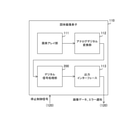
- FIG. 2 is a block diagram showing a configuration example of the solid-state image pickup device 110 according to the first embodiment of the present technology.
- the solid-state image sensor 110 includes a pixel array unit 111, an analog-to-digital conversion unit 112, a digital signal processing unit 200, and an output interface 113.
- a plurality of pixels are arranged in a two-dimensional grid pattern in the pixel array unit 111.
- Each of the pixels generates an analog pixel signal by photoelectric conversion within the video period and outputs it to the analog-to-digital conversion unit 112.
- the video period is a period of the frame period having the same length as the period of the vertical synchronization signal, which does not correspond to the vertical blanking period.
- the analog-digital conversion unit 112 converts a pixel signal into a digital signal within the video period and supplies it to the digital signal processing unit 200.
- an ADC Analog to Digital Converter
- each of the ADCs converts the pixel signal of the corresponding column into AD (Analog to Digital). do.
- the digital signal processing unit 200 performs various signal processing such as white balance correction and demosaic processing on the digital signal from the analog digital conversion unit 112 within the video period.
- the digital signal processing unit 200 supplies image data in which the processed digital signals are arranged to the output interface 113.
- the digital signal processing unit 200 detects the presence or absence of a failure of its own circuit within the vertical blanking period, and supplies an error notification indicating the detection result to the output interface 113.
- the output interface 113 outputs image data and error notification to the ECU 120.
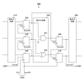
- FIG. 3 is a block diagram showing a configuration example of the digital signal processing unit 200 according to the first embodiment of the present technology.
- the digital signal processing unit 200 includes a scan test circuit 210, a scan LFSR 220, a controller 230, a signal processing circuit 240, and a scan MISR 250.
- the scan test circuit 210 performs a scan test on the signal processing circuit 240 within the vertical blanking period.
- the scan test circuit 210 includes a timing control unit 211, a seed value generation unit 212, and an error detection unit 213.
- the timing control unit 211 controls the start timing of the scan test.
- the timing control unit 211 drives the seed value generation unit 212, the error detection unit 213, and the controller 230 within the vertical blanking period within the period based on the vertical synchronization signal VSYNC.
- the seed value generation unit 212 generates a predetermined seed value for the scan LFSR 220 to generate a test pattern.
- the seed value generation unit 212 supplies the generated seed value to the scan LFSR 220.
- the error detection unit 213 detects the presence or absence of a failure in the signal processing circuit 240.
- the error detection unit 213 receives the compressed data obtained by compressing the scan test result from the scan MISR250. Then, the error detection unit 213 compares the compressed data with a predetermined expected value, and detects the presence or absence of a failure of the signal processing circuit 240 based on the comparison result.
- the error detection unit 213 generates an error notification indicating the detection result and supplies it to the output interface 113.
- the controller 230 controls the scan LFSR 220, the signal processing circuit 240, and the scan MISR 250.
- the controller 230 generates a predetermined clock signal CLK having a frequency higher than that of the vertical synchronization signal VSYNC and supplies it to the signal processing circuit 240.
- the controller 230 generates a test enable signal TESTEN according to the control of the timing control unit 211 and supplies it to the scan LFSR 220 and the scan MISR 250.
- the test enable signal TESTEN is a signal indicating whether or not the scan test is being executed, is set to be disabled during the video period, and is set to be enabled during the vertical blanking period.
- the controller 230 generates a scan enable signal ScanEN and inputs it to the signal processing circuit 240.
- the scan enable signal ScanEN is a signal for switching the input destination of the scan flip-flop in the signal processing circuit 240.
- the scan LFSR 220 generates a test pattern by LFSR based on the seed value.
- a digital signal from the analog-to-digital conversion unit 112, a seed value from the seed value generation unit 212, and a test enable signal TESTEN from the controller 230 are input to the scan LFSR 220.
- the scan LFSR 220 is an example of the test pattern generation circuit described in the claims.
- the scan LFSR 220 supplies the digital signal from the analog-to-digital conversion unit 112 to the signal processing circuit 240 as it is.
- the scan LFSR 220 generates a predetermined test pattern from the seed value and supplies it to the signal processing circuit 240.
- a predetermined number of flip-flops and a combinational circuit including a predetermined number of logic gates are arranged in the signal processing circuit 240.
- the signal processing circuit 240 executes signal processing in synchronization with the clock signal CLK, and supplies image data in which the processed digital signals are arranged to the scan MISR 250.
- the flip-flops in the signal processing circuit 240 are connected in series, and the test pattern is taken in synchronization with the clock signal CLK. Then, the combinational circuit in the signal processing circuit 240 executes a logical operation on the test pattern, and the flip-flop takes in the operation result.
- the flip-flop supplies the data including the calculation result to the scan MISR250 as a test result in synchronization with the clock signal CLK.
- Scan MISR250 compresses test results by MISR.
- the scan MISR 250 outputs the image data from the signal processing circuit 240 as it is to the output interface 113.
- the scan MISR 250 compresses the test result from the signal processing circuit 240 by MISR to generate compressed data, and supplies the compressed data to the error detection unit 213.
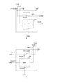
- FIG. 4 is a block diagram showing a configuration example of scan LFSR220 and scan MISR250 according to the first embodiment of the present technology.
- a is a block diagram showing a configuration example of the scan LFSR 220.
- Reference numeral b in the figure is a block diagram showing a configuration example of the scan MISR 250.
- the scan LFSR 220 includes a switch 221 and an LFSR 222.
- the switch 221 supplies the digital signal from the analog-to-digital conversion unit 112 to the signal processing circuit 240 when the test enable signal TESTEN is disabled.
- the LFSR222 generates a test pattern ScanIN based on the seed value from the scan test circuit 210 and supplies it to the signal processing circuit 240 when the test enable signal TESTEN is enabled.
- the scan MISR 250 includes a switch 251 and a MISR 252.
- the switch 251 supplies image data from the signal processing circuit 240 to the output interface 113 when the test enable signal TESTEN is disabled.
- the MISSR252 compresses the test result ScanOUT from the signal processing circuit 240 to generate compressed data when the test enable signal TESTEN is enabled, and supplies the compressed data to the scan test circuit 210.
- FIG. 5 is a block diagram showing a configuration example of the signal processing circuit 240 according to the first embodiment of the present technology.
- the signal processing circuit 240 includes a processing unit 300.
- the processing unit 300 processes the digital signal from the LFSR222 or the test pattern ScanIN, and supplies the processing result to the scan MISR250.
- a predetermined number of scan flip-flops such as scan flip-flops 320 are arranged in the processing unit 300.
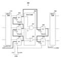
- FIG. 6 is a circuit diagram showing a configuration example of the processing unit 300 according to the first embodiment of the present technology.
- a predetermined number of combinational circuits such as combinational circuits 310, 350 and 380 and a predetermined number of scan flip-flops such as scan flip-flops 320, 330, 340, 360 and 370 are arranged in the processing unit 300.
- the combinational circuit 310 performs a predetermined logical operation on the input digital signal.
- the combinational circuit 310 is provided with a predetermined number of logic gates such as an AND (logical product) gate and an OR (logical sum) gate.
- the combinational circuit 310 supplies the processed digital signal to the scan flip-flops 320, 330 and 340.
- the scan flip-flop 340 captures either the digital signal from the combinational circuit 310 or the test pattern ScanIN from the scan LFSR 220 in synchronization with the clock signal CLK.
- the scan flip-flop 340 takes in the digital signal from the combinational circuit 310.
- the scan flip-flop 340 captures the test pattern ScanIN from the scan LFSR220. Then, the scan flip-flop 340 outputs the captured data to the scan flip-flop 330 and the combinational circuit 350 in synchronization with the clock signal CLK.
- the scan flip-flop 330 captures either the digital signal from the combinational circuit 310 or the test pattern ScanIN from the scan flip-flop 340 in synchronization with the clock signal CLK.
- the scan flip-flop 330 outputs the captured data to the scan flip-flop 320 and the combinational circuit 350 in synchronization with the clock signal CLK.
- the scan flip-flop 320 captures either the digital signal from the combinational circuit 310 or the test pattern ScanIN from the scan flip-flop 330 in synchronization with the clock signal CLK.
- the scan flip-flop 320 outputs the captured data to the scan flip-flop 360 and the combinational circuit 350 in synchronization with the clock signal CLK.
- the combinational circuit 350 performs a predetermined logical operation on the input digital signal.
- the combination circuit 350 is provided with a predetermined number of logic gates such as an AND gate 351 and an OR gate 352.
- the AND gate 351 calculates the logical product of the signal from the scan flip-flop 320 and the signal having the logic value "0", and supplies the signal to the scan flip-flop 360.
- the OR gate 352 calculates the logical sum of the signal from the scan flip-flop 330 and the signal from the scan flip-flop 340 and supplies the signal to the scan flip-flop 370.
- the scan flip-flop 360 captures either the signal from the combinational circuit 350 or the test pattern ScanIN from the scan flip-flop 320 in synchronization with the clock signal CLK.
- the scan flip-flop 360 outputs the captured data to the scan flip-flop 370 and the combinational circuit 380 in synchronization with the clock signal CLK.
- the scan flip-flop 370 captures either the signal from the combinational circuit 350 or the test pattern ScanIN from the scan flip-flop 360 in synchronization with the clock signal CLK.
- the scan flip-flop 370 outputs the captured data to the combinational circuit 380 and the scan MISR 250 in synchronization with the clock signal CLK.
- the data from the scan flip-flop 370 is output to the scan MISR250 as a test result ScanOUT.
- the combinational circuit 380 performs a predetermined logical operation on the input digital signal.
- the combinational circuit 380 supplies the calculation result to the circuit in the subsequent stage.
- the calculation result of the circuit in the subsequent stage is output to the scan MISR250 as image data.
- the number of scan flip-flops is not limited to five.
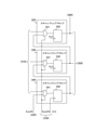
- FIG. 7 is a circuit diagram showing a configuration example of scan flip-flops 320, 330, and 340 according to the first embodiment of the present technology.
- the scan flip-flop 320 includes a selector 321 and a flip-flop 322.
- the scan flip-flop 330 includes a selector 331 and a flip-flop 332, and the scan flip-flop 340 includes a selector 341 and a flip-flop 342.
- the selector 341 selects either the digital signal from the combinational circuit 310 or the test pattern ScanIN according to the scan enable signal ScanEN and supplies it to the flip-flop 342.
- the flip-flop 342 takes in the data from the selector 341 in synchronization with the clock signal CLK.
- the flip-flop 342 outputs the captured data to the scan flip-flop 330 and the combinational circuit 350 in synchronization with the clock signal CLK.
- the circuit configurations of the scan flip-flops 320, 330, 360 and 370 are the same as those of the scan flip-flop 340.
- a predetermined number of scan flip-flops such as the scan flip-flop 320 are connected in series to form a shift register.
- This shift register captures and holds the test pattern ScanIN in synchronization with the clock signal CLK.
- N is an integer
- the N-bit test pattern ScanIN is input.
- the N-bit test pattern ScanIN is fetched bit by bit in order, and it takes N clocks to fetch all bits. In this way, the control of connecting a predetermined number of scan flip-flops in series, inputting a test pattern, and detecting the presence or absence of a failure of the combinational circuit is called a scan test.
- the circuit after the scan flip-flop (combination circuit 350, etc.) is the test target of the scan test.
- Scan flip-flops 320, 330, 340, and other flip-flops in the previous stage input a part of the test pattern ScanIN to the combinational circuit 350 to be tested.
- the combinational circuit 350 performs a logical operation on the input data, and outputs the result to the flip-flops of the previous stage such as the scan flip-flops 360 and 370.
- the flip-flops in the subsequent stages capture the calculation results.
- the data including the calculation result held in the scan flip-flops 360 and 370 in the subsequent stage and the data held in the scan flip-flops 320, 330 and 340 in the previous stage is output as a test result ScanOUT by N clock.
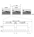
- FIG. 8 is a timing chart showing an example of the operation of the solid-state image sensor 110 according to the first embodiment of the present technology.
- the period from the rising edge (or falling edge) of the vertical synchronization signal to the next rising edge (or falling edge) is defined as the frame period.
- the frame period includes the vertical blanking period and other video periods.
- the period from timing T1 to T2 is set as the vertical blanking period.
- the period from timing T2 to T3 is set as the video period.
- the length of the vertical blanking period shall be shorter than the video period.
- the solid-state image sensor 110 captures image data.
- the solid-state image sensor 110 performs a scan test.
- the test enable signal TESTEN is disabled during the video period and enabled during the vertical blanking period.
- the vertical blanking period includes the scan-in period, the capture period, and the scan-out period.
- timings T1 to T11 are set as scan-in periods. The length of this scan-in period is set to N times the cycle of the clock signal CLK (that is, for N clocks) when the number of scan flip-flops is N.
- the timings T11 to T12 are set as the capture period. The length of the capture period is set to one clock of the clock signal CLK.
- the timings T12 to T13 are set as the scanout period.
- the length of the scanout period is set to be the same as the scanin period.
- the controller 230 enables the scan enable signal ScanEN, and the scan LFSR220 inputs the test pattern ScanIN.
- the scan enable signal ScanEN When enabled, for example, a high level scan enable signal ScanEN is supplied.
- a low-level scan enable signal ScanEN is supplied.
- the controller 230 disables the scan enable signal ScanEN and causes the calculation results to be captured by the scan flip-flops 360 and 370 in the subsequent stage.
- the controller 230 enables the scan enable signal ScanEN, and the scan flip-flop outputs the test result ScanOUT.
- the above procedure from scan-in to scan-out is not limited to one time, and the test pattern can be changed and executed multiple times as needed.
- the solid-state image sensor 110 can detect the presence or absence of a circuit failure during image pickup of a moving image by performing a scan test within the vertical blanking period. This makes it possible to improve the safety and reliability of the vehicle control system.
- a comparative example two circuits are provided, one is a path for processing pixel data and the other is a path for processing test data having the same value as the pixel data, and the results of each pass are compared to determine a circuit failure.
- a solid-state image sensor that detects the presence or absence. In this comparative example, it is necessary to drive both the path for processing the pixel data and the path for processing the test data within the video period.
- FIG. 9 is a diagram showing an example of the state of the processing unit 300 within the scan-in period in the first embodiment of the present technology.
- the scan flip-flops 320, 330, 340, 360 and 370 are connected in series to form a shift register.
- This shift register takes in the test pattern ScanIN bit by bit in synchronization with the clock signal CLK.
- the scan flip-flops 320, 330, 340, 360 and 370 capture the data of the logical values "0", "1", "0", "0" and "1", respectively.
- FIG. 10 is a diagram showing an example of the state of the processing unit 300 within the capture period in the first embodiment of the present technology.
- the AND gate 351 in the combination circuit 350 calculates the logical product of the logical value "0" from the scan flip-flop 320 and the predetermined logical value "0".
- the OR gate 352 calculates the logical sum of the logical values "1" and "0" from the scan flip-flops 330 and 340.
- the scan flip-flops 360 and 370 capture their calculation results.
- the scan test circuit 210 can detect the presence or absence of failure of the AND gate 351 and the OR gate 352 by comparing the data held in the scan flip-flops 360 and 370 with the expected value.
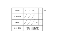
- FIG. 11 is a diagram showing an example of a test result, compressed data, expected value, and error notification in the first embodiment of the present technology.
- the scan flip-flop outputs, for example, data including "01011" as a test result ScanOUT.
- the scan MISR250 reduces unnecessary bits from the test result ScanOUT by compression.
- the scan MISR 250 generates, for example, data including "11" in which the first 3 bits are reduced as compressed data.
- the expected value of the compressed data output when there is no failure in the signal processing circuit shall include, for example, "01".
- the scan test circuit 210 compares the compressed data with the expected value, and identifies the location where the failure has occurred based on the comparison result. In the example of the figure, since only the first bit of the compressed data differs from the expected value, the scan test circuit 210 has a failure in the AND gate 351 corresponding to the first bit, and the OR gate 352 corresponding to the second bit. Judge that there is no failure. The scan test circuit 210 generates and outputs an error notification indicating the determination result.
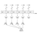
- FIG. 12 is a diagram for explaining the procedure of the scan test in the first embodiment of the present technology.
- the pixel array unit 111 generates a pixel signal
- the analog-to-digital conversion unit 112 AD-converts the pixel signal to generate a digital signal.
- the signal processing circuit 240 in the digital signal processing unit 200 performs predetermined signal processing on the digital signal from the analog digital conversion unit 112 within the video period. Further, the scan test circuit 210 performs a scan test on the signal processing circuit 240 within the vertical blanking period that does not correspond to the video period.
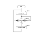
- FIG. 13 is a flowchart showing an example of the operation of the solid-state image pickup device 110 according to the first embodiment of the present technology. This operation is started, for example, when a predetermined application for capturing image data is executed.
- the scan test circuit 210 in the solid-state image sensor 110 performs a scan test (step S911).
- the solid-state image sensor 110 determines whether or not the vertical blanking period has elapsed (step S912). If the vertical blanking period has not elapsed (step S912: No), the solid-state image sensor 110 repeats step S912.
- step S912 when the vertical blanking period has elapsed (step S912: Yes), the solid-state image sensor 110 captures image data within the video period (step S913), and repeats steps S911 and subsequent steps.
- the scan test circuit 210 since the scan test circuit 210 performs the scan test within the vertical blanking period, the two paths are driven within the video period to check for the presence or absence of failure. Power consumption can be reduced as compared with the case of detection.
- the scan test circuit 210 outputs an error notification for each frame period, but in this configuration, the scan test cannot be performed for all the required patterns, and failure detection is performed. The rate may decrease.
- the solid-state image sensor 110 of the second embodiment is different from the first embodiment in that the test pattern is changed for each frame period.
- FIG. 14 is a timing chart showing an example of the operation of the solid-state image sensor 110 according to the second embodiment of the present technology.
- the scan test circuit 210 in the solid-state image sensor 110 of the second embodiment keeps the seed value constant within the vertical blanking period and changes the seed value each time the frame period elapses.
- the scan LFSR 220 changes the test pattern ScanIN every frame period based on its seed value.
- the scan LFSR 220 generates a number of test patterns that can obtain a failure detection rate equal to or higher than a predetermined value required in a vehicle control system. For example, when one type of test pattern is used, the failure detection rate is 70%, and when two types, three types and four types of test patterns are used, the failure detection rate is improved to 80%, 87% and 90%. do. Here, when a failure detection rate of 90% or more is required, four types of test patterns are used.
- the scan test circuit 210 performs a scan test for each frame period within a period in which a required number (4, etc.) of test patterns are sequentially generated, and outputs an error notification based on each test result.
- the scan test circuit 210 inputs the seed value A within the first vertical blanking period of the timings T1 and T2.
- the scan test circuit 210 compares the first test result ScanOUT with the expected value, and holds the comparison result. At this point, no error notification is output.
- the scan test circuit 210 changes the seed value to B and changes the test pattern.
- the scan test circuit 210 compares the second test result ScanOUT with the expected value, and holds the comparison result. At this point, no error notification is output.
- the scan test circuit 210 changes the seed value to C and changes the test pattern.
- the scan test circuit 210 compares the third test result ScanOUT with the expected value, and holds the comparison result. At this point, no error notification is output.
- the scan test circuit 210 changes the seed value to D and changes the test pattern.
- the scan test circuit 210 compares the fourth test result ScanOUT with the expected value. Then, the scan test circuit 210 detects the presence or absence of a failure based on the respective comparison results from the first to the fourth, and generates an error notification. For example, if one or more of the four comparison results for a certain circuit A indicate a failure of the circuit, the scan test circuit 210 determines that the circuit A has a failure. On the other hand, if all of the four comparison results indicate that there is no failure, the scan test circuit 210 determines that the circuit A has no failure.
- the scan test circuit 210 returns the seed value to the initial value. After that, the same procedure is repeated and executed in a 4-frame cycle.
- the scan test circuit 210 can perform a scan test using a plurality of test patterns and improve the failure detection rate.
- the scan test circuit 210 changes the test pattern for each frame period, the scan test can be performed using a plurality of test patterns. As a result, the failure detection rate can be improved as compared with the first embodiment in which the test pattern is not changed.
- the scan test circuit 210 inputs N-bit test patterns to N scan flip-flops, but in this configuration, as the number of scan flip-flops increases, scans are performed. The test takes longer.
- the solid-state image sensor 110 of the third embodiment is different from the first embodiment in that the signal processing circuit 240 is divided into a plurality of processing units and a scan test is performed in parallel for each processing unit.
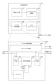
- FIG. 15 is a block diagram showing a configuration example of the signal processing circuit 240 according to the third embodiment of the present technology.
- the signal processing circuit 240 of the third embodiment is divided into a processing unit 300 and a processing unit 400.
- the processing unit 300 is an example of the first processing unit described in the claims
- the processing unit 400 is an example of the second processing unit described in the claims.
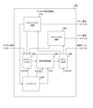
- FIG. 16 is a block diagram showing a configuration example of the digital signal processing unit 200 according to the third embodiment of the present technology.
- the digital signal processing unit 200 of the third embodiment is different from the first embodiment in that it further includes a scan test circuit 260.
- the scan test circuit 260 performs a scan test on the processing unit 400 within the vertical blanking period.
- the scan test circuit 260 detects the presence or absence of a failure in the processing unit 400, and supplies an error notification indicating the result to the output interface 113.
- the scan test circuit 210 is an example of the first test circuit described in the claims, and the scan test circuit 260 is an example of the second test circuit described in the claims.
- FIG. 17 is a timing chart showing an example of the operation of the solid-state image sensor 110 according to the third embodiment of the present technology.
- the scan test circuit 210 performs a scan test on the processing unit 300, and the scan test circuit 210 performs a scan test on the processing unit 400 within the vertical blanking period. In this way, by performing the scan test in parallel for each of the plurality of processing units, the time required for the scan test can be shortened.
- the number of each scan flip-flop is less than N by dividing the signal processing circuit 240 into the processing unit 300 and the processing unit 400. can do.
- the scan-in and scan-out periods can be shortened as compared with the case where the division is not performed.
- the signal processing circuit 240 is divided into two processing units, it can also be divided into three or more. In this case, three or more scan test circuits are arranged.
- the second embodiment can be applied to the third embodiment.
- the scan test circuit 210 scan-tests the processing unit 300, and the scan test circuit 260 scan-tests the processing unit 400, so that the plurality of processing units are parallel to each other. You can do a scan test on it. This can reduce the time required for the scan test.
- the scan test circuit 210 detects the presence or absence of a failure of the signal processing circuit 240, but when the scan test circuit 210 itself fails, the failure detection of the signal processing circuit 240 The rate may decrease.
- the solid-state image sensor 110 of the fourth embodiment is different from the first embodiment in that it further detects the presence or absence of a failure of the scan test circuit 210.
- FIG. 18 is a block diagram showing a configuration example of the digital signal processing unit 200 according to the fourth embodiment of the present technology.
- the digital signal processing unit 200 is different from the first embodiment in that it further includes a failure detection circuit 270.
- the failure detection circuit 270 detects the presence or absence of a failure in the scan test circuit 210. It is assumed that the detection of the presence or absence of failure of the scan test circuit 210 is not executed for each frame, but is executed for each M (M is an integer of 2 or more) frames.
- the failure detection circuit 270 generates a seed value S2 and supplies it to the scan LFSR 220 at the timing of detecting the failure.
- the seed value S2 is different from the seed value S1 generated by the scan test circuit 210, and when a scan test is performed using the seed value S2, the seed value S2 is different from the expected value even if the signal processing circuit 240 has no failure. This is the value from which the test result can be obtained.
- the scan LFSR220 of the fourth embodiment When the seed value S2 is generated, the scan LFSR220 of the fourth embodiment generates a test pattern from the seed value S2 instead of the seed value S1.
- the scan test circuit 210 of the fourth embodiment also supplies an error notification to the failure detection circuit 270. Based on the error notification, the failure detection circuit 270 determines whether or not a failure has been detected in the signal processing circuit 240 when the seed value S2 is supplied.
- the failure detection circuit 270 determines that there is no failure in the scan test circuit 210. On the other hand, when the failure is not detected in the signal processing circuit 240, the failure detection circuit 270 determines that the failure has occurred in the scan test circuit 210. The failure detection circuit 270 generates a detection signal indicating the presence or absence of a failure in the scan test circuit 210 and supplies it to the output interface 113.
- failure detection circuit 270 can also generate input data for which the expected value cannot be obtained and input it to the signal processing circuit 240 instead of the seed value S2.
- FIG. 19 is a timing chart showing an example of the operation of the solid-state image pickup device 110 when the scan test circuit 210 in the fourth embodiment of the present technology fails.
- the failure detection circuit 270 switches the seed value. Since the scan test circuit 210 is out of order, it is determined that there is no failure in the combinational circuit and an error notification is output even though the expected value cannot be obtained. The failure detection circuit 270 determines that a failure has occurred in the scan test circuit 210 based on the error notification.
- FIG. 20 is a timing chart showing an example of the operation of the solid-state image pickup device 110 when the scan test circuit 210 according to the fourth embodiment of the present technology is not broken.
- the failure detection circuit 270 switches the seed value. Since the scan test circuit 210 is normal, it is determined again that a failure has occurred in the combinational circuit, and an error notification is output. The failure detection circuit 270 determines that the scan test circuit 210 has not failed based on the error notification.
- the failure detection circuit 270 can detect the presence or absence of a failure in the scan test circuit 210. As a result, the failure detection rate of the signal processing circuit 240 can be improved.
- the failure detection circuit 270 detects the presence or absence of a failure in the scan test circuit 210, the failure detection rate of the signal processing circuit 240 to be scan-tested is further improved. Can be made to.
- the technology according to the present disclosure (this technology) can be applied to various products.
- the technology according to the present disclosure is realized as a device mounted on a moving body of any kind such as an automobile, an electric vehicle, a hybrid electric vehicle, a motorcycle, a bicycle, a personal mobility, an airplane, a drone, a ship, and a robot. You may.
- FIG. 21 is a block diagram showing a schematic configuration example of a vehicle control system, which is an example of a mobile control system to which the technique according to the present disclosure can be applied.
- the vehicle control system 12000 includes a plurality of electronic control units connected via the communication network 12001.
- the vehicle control system 12000 includes a drive system control unit 12010, a body system control unit 12020, an outside information detection unit 12030, an in-vehicle information detection unit 12040, and an integrated control unit 12050.
- a microcomputer 12051, an audio image output unit 12052, and an in-vehicle network I / F (interface) 12053 are shown as a functional configuration of the integrated control unit 12050.
- the drive system control unit 12010 controls the operation of the device related to the drive system of the vehicle according to various programs.
- the drive system control unit 12010 has a driving force generator for generating a driving force of a vehicle such as an internal combustion engine or a driving motor, a driving force transmission mechanism for transmitting the driving force to the wheels, and a steering angle of the vehicle. It functions as a control device such as a steering mechanism for adjusting and a braking device for generating braking force of the vehicle.
- the body system control unit 12020 controls the operation of various devices mounted on the vehicle body according to various programs.
- the body system control unit 12020 functions as a keyless entry system, a smart key system, a power window device, or a control device for various lamps such as headlamps, back lamps, brake lamps, turn signals or fog lamps.
- the body system control unit 12020 may be input with radio waves transmitted from a portable device that substitutes for the key or signals of various switches.
- the body system control unit 12020 receives inputs of these radio waves or signals and controls a vehicle door lock device, a power window device, a lamp, and the like.
- the vehicle outside information detection unit 12030 detects information outside the vehicle equipped with the vehicle control system 12000.
- the image pickup unit 12031 is connected to the vehicle outside information detection unit 12030.
- the vehicle outside information detection unit 12030 causes the image pickup unit 12031 to capture an image of the outside of the vehicle and receives the captured image.
- the out-of-vehicle information detection unit 12030 may perform object detection processing or distance detection processing such as a person, a vehicle, an obstacle, a sign, or a character on the road surface based on the received image.
- the image pickup unit 12031 is an optical sensor that receives light and outputs an electric signal according to the amount of the light received.
- the image pickup unit 12031 can output an electric signal as an image or can output it as distance measurement information. Further, the light received by the image pickup unit 12031 may be visible light or invisible light such as infrared light.
- the in-vehicle information detection unit 12040 detects the in-vehicle information.
- a driver state detection unit 12041 that detects the driver's state is connected to the in-vehicle information detection unit 12040.
- the driver state detection unit 12041 includes, for example, a camera that images the driver, and the in-vehicle information detection unit 12040 determines the degree of fatigue or concentration of the driver based on the detection information input from the driver state detection unit 12041. It may be calculated, or it may be determined whether the driver has fallen asleep.
- the microcomputer 12051 calculates the control target value of the driving force generator, the steering mechanism, or the braking device based on the information inside and outside the vehicle acquired by the vehicle exterior information detection unit 12030 or the vehicle interior information detection unit 12040, and the drive system control unit.
- a control command can be output to 12010.
- the microcomputer 12051 realizes ADAS (Advanced Driver Assistance System) functions including vehicle collision avoidance or impact mitigation, follow-up driving based on inter-vehicle distance, vehicle speed maintenance driving, vehicle collision warning, vehicle lane deviation warning, and the like. It is possible to perform cooperative control for the purpose of.
- ADAS Advanced Driver Assistance System
- the microcomputer 12051 controls the driving force generating device, the steering mechanism, the braking device, and the like based on the information around the vehicle acquired by the vehicle exterior information detection unit 12030 or the vehicle interior information detection unit 12040. It is possible to perform coordinated control for the purpose of automatic driving that runs autonomously without depending on the operation.
- the microcomputer 12051 can output a control command to the body system control unit 12020 based on the information outside the vehicle acquired by the vehicle outside information detection unit 12030.
- the microcomputer 12051 controls the headlamps according to the position of the preceding vehicle or the oncoming vehicle detected by the outside information detection unit 12030, and performs cooperative control for the purpose of anti-glare such as switching the high beam to the low beam. It can be carried out.
- the audio image output unit 12052 transmits an output signal of at least one of audio and an image to an output device capable of visually or audibly notifying information to the passenger or the outside of the vehicle.
- an audio speaker 12061, a display unit 12062, and an instrument panel 12063 are exemplified as output devices.
- the display unit 12062 may include, for example, at least one of an onboard display and a head-up display.
- FIG. 22 is a diagram showing an example of the installation position of the image pickup unit 12031.
- the image pickup unit 12101, 12102, 12103, 12104, 12105 is provided.
- the image pickup units 12101, 12102, 12103, 12104, 12105 are provided, for example, at positions such as the front nose, side mirrors, rear bumpers, back doors, and the upper part of the windshield in the vehicle interior of the vehicle 12100.
- the image pickup unit 12101 provided in the front nose and the image pickup section 12105 provided in the upper part of the windshield in the vehicle interior mainly acquire an image in front of the vehicle 12100.
- the image pickup units 12102 and 12103 provided in the side mirror mainly acquire images of the side of the vehicle 12100.
- the image pickup unit 12104 provided in the rear bumper or the back door mainly acquires an image of the rear of the vehicle 12100.
- the image pickup unit 12105 provided on the upper part of the windshield in the vehicle interior is mainly used for detecting a preceding vehicle, a pedestrian, an obstacle, a traffic light, a traffic sign, a lane, or the like.
- FIG. 22 shows an example of the shooting range of the imaging units 12101 to 12104.
- the imaging range 12111 indicates the imaging range of the imaging unit 12101 provided on the front nose
- the imaging ranges 12112 and 12113 indicate the imaging range of the imaging units 12102 and 12103 provided on the side mirrors, respectively
- the imaging range 12114 indicates the imaging range.
- the imaging range of the imaging unit 12104 provided on the rear bumper or the back door is shown. For example, by superimposing the image data captured by the image pickup units 12101 to 12104, a bird's-eye view image of the vehicle 12100 can be obtained.
- At least one of the image pickup units 12101 to 12104 may have a function of acquiring distance information.
- at least one of the image pickup units 12101 to 12104 may be a stereo camera including a plurality of image pickup elements, or may be an image pickup element having pixels for phase difference detection.
- the microcomputer 12051 has a distance to each three-dimensional object within the image pickup range 12111 to 12114 based on the distance information obtained from the image pickup unit 12101 to 12104, and a temporal change of this distance (relative speed with respect to the vehicle 12100). By obtaining can. Further, the microcomputer 12051 can set an inter-vehicle distance to be secured in advance in front of the preceding vehicle, and can perform automatic braking control (including follow-up stop control), automatic acceleration control (including follow-up start control), and the like. In this way, it is possible to perform coordinated control for the purpose of automatic driving or the like in which the vehicle travels autonomously without depending on the operation of the driver.
- automatic braking control including follow-up stop control
- automatic acceleration control including follow-up start control
- the microcomputer 12051 converts three-dimensional object data related to a three-dimensional object into two-wheeled vehicles, ordinary vehicles, large vehicles, pedestrians, electric poles, and other three-dimensional objects based on the distance information obtained from the image pickup units 12101 to 12104. It can be classified and extracted and used for automatic avoidance of obstacles. For example, the microcomputer 12051 distinguishes obstacles around the vehicle 12100 into obstacles that are visible to the driver of the vehicle 12100 and obstacles that are difficult to see. Then, the microcomputer 12051 determines the collision risk indicating the risk of collision with each obstacle, and when the collision risk is equal to or higher than the set value and there is a possibility of collision, the microcomputer 12051 via the audio speaker 12061 or the display unit 12062. By outputting an alarm to the driver and performing forced deceleration and avoidance steering via the drive system control unit 12010, driving support for collision avoidance can be provided.
- At least one of the image pickup units 12101 to 12104 may be an infrared camera that detects infrared rays.
- the microcomputer 12051 can recognize a pedestrian by determining whether or not a pedestrian is present in the captured image of the imaging unit 12101 to 12104.
- pedestrian recognition is, for example, a procedure for extracting feature points in an image captured by an image pickup unit 12101 to 12104 as an infrared camera, and pattern matching processing is performed on a series of feature points indicating the outline of an object to determine whether or not the pedestrian is a pedestrian. It is done by the procedure to determine.
- the audio image output unit 12052 determines the square contour line for emphasizing the recognized pedestrian.
- the display unit 12062 is controlled so as to superimpose and display. Further, the audio image output unit 12052 may control the display unit 12062 so as to display an icon or the like indicating a pedestrian at a desired position.
- the above is an example of a vehicle control system to which the technology according to the present disclosure can be applied.
- the technique according to the present disclosure can be applied to, for example, the image pickup unit 12031 among the configurations described above.
- the solid-state image sensor 110 of FIG. 2 can be applied to the image pickup unit 12031.
- the present technology can have the following configurations.
- An analog-to-digital converter that generates a digital signal within a predetermined video period
- a signal processing circuit that performs predetermined signal processing on the digital signal within the video period
- a solid-state image sensor including a scan test circuit that performs a scan test on the signal processing circuit within a vertical blanking period that does not correspond to the video period.
- the scan test circuit performs the scan test in each of a plurality of frame periods including the vertical blanking period, and an error notification indicating the presence or absence of a failure of the signal processing circuit based on each test result.
- the solid-state image pickup device according to (1) above.
- a test pattern generation circuit that generates a predetermined test pattern based on the input seed value and inputs it to the signal processing circuit is further provided.
- the solid-state image pickup device according to (2) above, wherein the scan test circuit changes the seed value each time the frame period elapses.
- the scan test circuit includes first and second test circuits.
- the signal processing circuit includes first and second processing units. The first test circuit performs a scan test on the first processing unit and performs a scan test.
- the solid-state image pickup device according to any one of (1) to (3) above, wherein the second test circuit performs a scan test on the second processing unit.
- the solid-state image pickup device according to any one of (1) to (4), further comprising a failure detection circuit for detecting the presence or absence of a failure in the scan test circuit.
- a test pattern generation circuit that generates a predetermined test pattern based on the input seed value and inputs it to the signal processing circuit is further provided.
- the signal processing circuit is With a predetermined number of scan flip-flops.
- the solid-state image pickup device according to any one of (1) to (5), further comprising a combinational circuit that performs a predetermined logical operation on the data output from the scan flip-flop.
- An analog-to-digital converter that generates a digital signal within a predetermined video period, a signal processing circuit that performs predetermined signal processing on the digital signal within the video period, and a vertical panel that does not correspond to the video period.
- a solid-state image sensor equipped with a scan test circuit that performs a scan test on the signal processing circuit within the ranking period, and A vehicle control system including a control unit for stopping the solid-state image sensor based on the result of the scan test.
- Solid-state image sensor 111 Pixel array unit 112 Analog-to-digital converter 113 Output interface 120 ECU 130 Display unit 200 Digital signal processing unit 210, 260 Scan test circuit 211 Timing control unit 212 Seed value generation unit 213 Error detection unit 220 Scan LFSR 221 and 251 switches 222 LFSR 230 Controller 240 Signal processing circuit 250 Scan MISR 252 MISS 270 Failure detection circuit 300, 400 Processing unit 310, 350, 380 Combination circuit 320, 330, 340, 360, 370 Scan flip-flop 321, 331, 341 Selector 322, 332, 342 Flip-flop 351 AND (logical product) Gate 352 OR (OR) Gate 12031 Imaging unit
Landscapes
- Engineering & Computer Science (AREA)
- Multimedia (AREA)
- Signal Processing (AREA)
- General Engineering & Computer Science (AREA)
- Physics & Mathematics (AREA)
- General Physics & Mathematics (AREA)
- Tests Of Electronic Circuits (AREA)
- Transforming Light Signals Into Electric Signals (AREA)
Abstract
撮像中に故障の有無を検出する固体撮像素子において、消費電力を削減する。 固体撮像素子は、アナログデジタル変換部、信号処理回路、および、スキャンテスト回路を具備する。アナログデジタル変換部は、所定の映像期間内にデジタル信号を生成する。信号処理回路は、映像期間内にデジタル信号に対して所定の信号処理を行う。スキャンテスト回路は、映像期間に該当しない垂直ブランキング期間内に信号処理回路に対してスキャンテストを行う。
Description
本技術は、固体撮像素子に関する。詳しくは、回路の故障の有無を検出する固体撮像素子、車両制御システム、および、固体撮像素子の制御方法に関する。
従来より、特に車載カメラに用いられる固体撮像素子においては、安全性や信頼性を確保する観点から、その素子自身が故障の有無を検出するBIST(Built-In Self Test)機能が要求されることが多い。例えば、画素データを処理するパスと、その画素データと同じ値のテストデータを処理するパスとの2系統の回路を設け、それぞれのパスの結果を比較して回路の故障の有無を検出する固体撮像素子が提案されている(例えば、特許文献1参照。)。
上述の従来技術では、2系統のそれぞれのパスの結果の比較により、撮像中に、回路の故障の有無を検出することを図っている。しかしながら、上述の固体撮像素子では、2系統のパスのそれぞれを形成する回路を撮像中に同時に駆動する必要があり、1系統のみを駆動する場合と比較して消費電力が増大するおそれがある。
本技術はこのような状況に鑑みて生み出されたものであり、撮像中に故障の有無を検出する固体撮像素子において、消費電力を削減することを目的とする。
本技術は、上述の問題点を解消するためになされたものであり、その第1の側面は、所定の映像期間内にデジタル信号を生成するアナログデジタル変換部と、上記映像期間内に上記デジタル信号に対して所定の信号処理を行う信号処理回路と、上記映像期間に該当しない垂直ブランキング期間内に上記信号処理回路に対してスキャンテストを行うスキャンテスト回路とを具備する固体撮像素子、および、その制御方法である。これにより、信号処理回路の故障の有無が検出されるという作用をもたらす。
また、この第1の側面において、上記スキャンテスト回路は、各々が上記垂直ブランキング期間を含む複数のフレーム期間のそれぞれにおいて上記スキャンテストを行い、それぞれのテスト結果に基づいて上記信号処理回路の故障の有無を示すエラー通知を出力してもよい。これにより、故障検出率が向上するという作用をもたらす。
また、この第1の側面において、入力されたシード値に基づいて所定のテストパターンを生成して上記信号処理回路に入力するテストパターン生成回路をさらに具備し、上記スキャンテスト回路は、フレーム期間が経過するたびに上記シード値を変更してもよい。これにより、フレーム期間ごとにテストパターンが変更されるという作用をもたらす。
また、この第1の側面において、上記スキャンテスト回路は、第1および第2のテスト回路を含み、上記信号処理回路は、第1および第2の処理部を含み、上記第1のテスト回路は、上記第1の処理部に対するスキャンテストを行い、上記第2のテスト回路は、上記第2の処理部に対するスキャンテストを行ってもよい。これにより、スキャンテストに要する時間が短くなるという作用をもたらす。
また、この第1の側面において、上記スキャンテスト回路の故障の有無を検出する故障検出回路をさらに具備してもよい。これにより、スキャンテスト対象の回路の故障検出率が向上するという作用をもたらす。
また、この第1の側面において、入力されたシード値に基づいて所定のテストパターンを生成して上記信号処理回路に入力するテストパターン生成回路をさらに具備し、上記信号処理回路は、所定数のスキャンフリップフロップと、上記スキャンフリップフロップから出力されたデータに対して所定の論理演算を行う組合せ回路とを備えてもよい。これにより、組合せ回路の故障が検出されるという作用をもたらす。
また、本技術の第2の側面は、所定の映像期間内にデジタル信号を生成するアナログデジタル変換部と、上記映像期間内に上記デジタル信号に対して所定の信号処理を行う信号処理回路と、上記映像期間に該当しない垂直ブランキング期間内に上記信号処理回路に対してスキャンテストを行うスキャンテスト回路とを備える固体撮像素子と、上記スキャンテストの結果に基づいて上記固体撮像素子を停止させる制御部とを具備する車両制御システムである。これにより、車両制御システムの安全性、信頼性が向上するという作用をもたらす。
以下、本技術を実施するための形態(以下、実施の形態と称する)について説明する。説明は以下の順序により行う。
1.第1の実施の形態(垂直ブランキング期間内にスキャンテストを行う例)
2.第2の実施の形態(垂直ブランキング期間内にスキャンテストを行い、フレームごとにテストパターンを変更する例)
3.第3の実施の形態(垂直ブランキング期間内に複数の処理部に対して並列にスキャンテストを行う例)
4.第4の実施の形態(垂直ブランキング期間内にスキャンテストを行い、スキャンテスト回路の故障を検出する例)
5.移動体への応用例
1.第1の実施の形態(垂直ブランキング期間内にスキャンテストを行う例)
2.第2の実施の形態(垂直ブランキング期間内にスキャンテストを行い、フレームごとにテストパターンを変更する例)
3.第3の実施の形態(垂直ブランキング期間内に複数の処理部に対して並列にスキャンテストを行う例)
4.第4の実施の形態(垂直ブランキング期間内にスキャンテストを行い、スキャンテスト回路の故障を検出する例)
5.移動体への応用例
<1.第1の実施の形態>
[車両制御システムの構成例]
図1は、本技術の第1の実施の形態における車両制御システムの一構成例を示すブロック図である。この車両制御システムは、自動車などの移動体を制御するためのシステムであり、固体撮像素子110、ECU(Electronic Control Unit)120および表示部130を備える。
[車両制御システムの構成例]
図1は、本技術の第1の実施の形態における車両制御システムの一構成例を示すブロック図である。この車両制御システムは、自動車などの移動体を制御するためのシステムであり、固体撮像素子110、ECU(Electronic Control Unit)120および表示部130を備える。
固体撮像素子110は、垂直同期信号に同期して、画像データを撮像するものである。垂直同期信号は、撮像のタイミングを指示する周期信号である。垂直同期信号の周波数は、例えば、30ヘルツ(Hz)に設定される。
固体撮像素子110は、撮像した画像データをECU120に供給する。また、固体撮像素子110は、自身の故障の有無を検出し、その検出結果を示すエラー通知をECU120に供給する。故障の検出タイミングについては後述する。
ECU120は、固体撮像素子110を内蔵したカメラなどの、車載の機器や装置を電子的に制御するものである。このECU120は、固体撮像素子110の撮像した画像データ(言い換えれば、フレーム)を表示部130に表示させる。また、ECU120は、固体撮像素子110に故障が発生した場合に固体撮像素子110に停止制御信号を供給して撮像動作を停止させ、故障が生じた旨や故障の内容を表示部130に表示させる。なお、ECU120は、特許請求の範囲に記載の制御部の一例である。
表示部130は、画像データなどの様々なデータを表示するものである。なお、ECU120は、故障が発生した場合に、固体撮像素子110を停止させず、黒画像などにマスクすることもできる。
なお、固体撮像素子110を車両制御システムに設けているが、車両制御システム以外のシステムや装置に固体撮像素子110を設けることもできる。例えば、FA(Factory Automation)システムに固体撮像素子110を設けてもよい。
[固体撮像素子の構成例]
図2は、本技術の第1の実施の形態における固体撮像素子110の一構成例を示すブロック図である。この固体撮像素子110は、画素アレイ部111、アナログデジタル変換部112、デジタル信号処理部200および出力インターフェース113を備える。
図2は、本技術の第1の実施の形態における固体撮像素子110の一構成例を示すブロック図である。この固体撮像素子110は、画素アレイ部111、アナログデジタル変換部112、デジタル信号処理部200および出力インターフェース113を備える。
画素アレイ部111には、複数の画素が二次元格子状に配列される。画素のそれぞれは、映像期間内に光電変換により、アナログの画素信号を生成してアナログデジタル変換部112に出力する。ここで、映像期間は、垂直同期信号の周期と同じ長さのフレーム期間のうち、垂直ブランキング期間に該当しない期間である。
アナログデジタル変換部112は、映像期間内に画素信号をデジタル信号に変換し、デジタル信号処理部200に供給するものである。このアナログデジタル変換部112には、例えば、画素アレイ部111の列ごとに、ADC(Analog to Digital Converter)が配列され、ADCのそれぞれは、対応する列の画素信号をAD(Analog to Digital)変換する。
デジタル信号処理部200は、映像期間内にアナログデジタル変換部112からのデジタル信号に対して、ホワイトバランス補正やデモザイク処理などの様々な信号処理を行うものである。このデジタル信号処理部200は、処理後のデジタル信号を配列した画像データを出力インターフェース113に供給する。
また、デジタル信号処理部200は、垂直ブランキング期間内に自身の回路の故障の有無を検出し、その検出結果を示すエラー通知を出力インターフェース113に供給する。
出力インターフェース113は、画像データとエラー通知とをECU120に出力するものである。
[デジタル信号処理部の構成例]
図3は、本技術の第1の実施の形態におけるデジタル信号処理部200の一構成例を示すブロック図である。このデジタル信号処理部200は、スキャンテスト回路210、スキャンLFSR220、コントローラ230、信号処理回路240およびスキャンMISR250を備える。
図3は、本技術の第1の実施の形態におけるデジタル信号処理部200の一構成例を示すブロック図である。このデジタル信号処理部200は、スキャンテスト回路210、スキャンLFSR220、コントローラ230、信号処理回路240およびスキャンMISR250を備える。
スキャンテスト回路210は、垂直ブランキング期間内に、信号処理回路240に対してスキャンテストを行うものである。このスキャンテスト回路210は、タイミング制御部211、シード値生成部212、および、エラー検出部213を備える。
タイミング制御部211は、スキャンテストの開始タイミングを制御するものである。このタイミング制御部211は、垂直同期信号VSYNCに基づいて、その周期内の垂直ブランキング期間内に、シード値生成部212、エラー検出部213およびコントローラ230を駆動する。
シード値生成部212は、スキャンLFSR220がテストパターンを生成するための所定のシード値を生成するものである。このシード値生成部212は、生成したシード値をスキャンLFSR220に供給する。
エラー検出部213は、信号処理回路240の故障の有無を検出するものである。このエラー検出部213は、スキャンテストの結果を圧縮した圧縮データをスキャンMISR250から受け取る。そして、エラー検出部213は、圧縮データと、所定の期待値とを比較して、その比較結果に基づいて信号処理回路240の故障の有無を検出する。エラー検出部213は、検出結果を示すエラー通知を生成し、出力インターフェース113に供給する。
コントローラ230は、スキャンLFSR220、信号処理回路240およびスキャンMISR250を制御するものである。このコントローラ230は、垂直同期信号VSYNCよりも周波数の高い所定のクロック信号CLKを生成し、信号処理回路240に供給する。
また、コントローラ230は、タイミング制御部211の制御に従ってテストイネーブル信号TESTENを生成し、スキャンLFSR220およびスキャンMISR250に供給する。テストイネーブル信号TESTENは、スキャンテストを実行中か否かを示す信号であり、映像期間内にディセーブルに設定され、垂直ブランキング期間内にイネーブルに設定される。
また、コントローラ230は、スキャンイネーブル信号ScanENを生成し、信号処理回路240に入力する。スキャンイネーブル信号ScanENは、信号処理回路240内のスキャンフリップフロップの入力先を切り替えるための信号である。
スキャンLFSR220は、シード値に基づいてLFSRによりテストパターンを生成するものである。このスキャンLFSR220には、アナログデジタル変換部112からのデジタル信号と、シード値生成部212からのシード値と、コントローラ230からのテストイネーブル信号TESTENとが入力される。なお、スキャンLFSR220は、特許請求の範囲に記載のテストパターン生成回路の一例である。
テストイネーブル信号TESTENがディセーブルの場合にスキャンLFSR220は、アナログデジタル変換部112からのデジタル信号をそのまま信号処理回路240に供給する。一方、テストイネーブル信号TESTENがイネーブルの場合にスキャンLFSR220は、シード値から所定のテストパターンを生成し、信号処理回路240に供給する。
信号処理回路240には、所定数のフリップフロップと、所定数の論理ゲートを含む組合せ回路とが配置される。この信号処理回路240は、クロック信号CLKに同期して信号処理を実行し、処理後のデジタル信号を配列した画像データをスキャンMISR250に供給する。
また、スキャンイネーブル信号ScanENがイネーブルの場合に信号処理回路240内のフリップフロップは直列に接続され、クロック信号CLKに同期してテストパターンを取り込む。そして、信号処理回路240内の組合せ回路は、テストパターンに対して論理演算を実行し、フリップフロップは、その演算結果を取り込む。フリップフロップは、クロック信号CLKに同期して、演算結果を含むデータをテスト結果としてスキャンMISR250に供給する。
スキャンMISR250は、MISRによりテスト結果を圧縮するものである。テストイネーブル信号TESTENがディセーブルの場合にスキャンMISR250は、信号処理回路240からの画像データをそのまま出力インターフェース113に出力する。
一方、テストイネーブル信号TESTENがイネーブルの場合にスキャンMISR250は、信号処理回路240からのテスト結果をMISRにより圧縮して圧縮データを生成し、エラー検出部213に供給する。
図4は、本技術の第1の実施の形態におけるスキャンLFSR220およびスキャンMISR250の一構成例を示すブロック図である。同図におけるaは、スキャンLFSR220の一構成例を示すブロック図である。同図におけるbは、スキャンMISR250の一構成例を示すブロック図である。
同図におけるaに例示するように、スキャンLFSR220は、スイッチ221およびLFSR222を備える。スイッチ221は、テストイネーブル信号TESTENがディセーブルの場合に、アナログデジタル変換部112からのデジタル信号を信号処理回路240に供給するものである。
LFSR222は、テストイネーブル信号TESTENがイネーブルの場合に、スキャンテスト回路210からのシード値に基づいてテストパターンScanINを生成し、信号処理回路240に供給するものである。
同図におけるbに例示するように、スキャンMISR250は、スイッチ251およびMISR252を備える。スイッチ251は、テストイネーブル信号TESTENがディセーブルの場合に、信号処理回路240からの画像データを出力インターフェース113に供給するものである。
MISR252は、テストイネーブル信号TESTENがイネーブルの場合に、信号処理回路240からのテスト結果ScanOUTを圧縮して圧縮データを生成し、スキャンテスト回路210に供給するものである。
[信号処理回路の構成例]
図5は、本技術の第1の実施の形態における信号処理回路240の一構成例を示すブロック図である。この信号処理回路240は、処理部300を備える。処理部300は、LFSR222からのデジタル信号またはテストパターンScanINを処理し、その処理結果をスキャンMISR250に供給するものである。処理部300内には、スキャンフリップフロップ320などの所定数のスキャンフリップフロップが配列される。
図5は、本技術の第1の実施の形態における信号処理回路240の一構成例を示すブロック図である。この信号処理回路240は、処理部300を備える。処理部300は、LFSR222からのデジタル信号またはテストパターンScanINを処理し、その処理結果をスキャンMISR250に供給するものである。処理部300内には、スキャンフリップフロップ320などの所定数のスキャンフリップフロップが配列される。
図6は、本技術の第1の実施の形態における処理部300の一構成例を示す回路図である。この処理部300には、組合せ回路310、350および380などの所定数の組合せ回路と、スキャンフリップフロップ320、330、340、360および370などの所定数のスキャンフリップフロップとが配置される。
組合せ回路310は、入力されたデジタル信号に対して所定の論理演算を行うものである。この組合せ回路310には、AND(論理積)ゲートやOR(論理和)ゲートなどの所定数の論理ゲートが設けられる。組合せ回路310は、処理後のデジタル信号をスキャンフリップフロップ320、330および340に供給する。
スキャンフリップフロップ340は、組合せ回路310からのデジタル信号と、スキャンLFSR220からのテストパターンScanINとのいずれかを、クロック信号CLKに同期して取り込むものである。
スキャンイネーブル信号ScanENがディセーブルの場合に、スキャンフリップフロップ340は、組合せ回路310からのデジタル信号を取り込む。一方、スキャンイネーブル信号ScanENがイネーブルの場合に、スキャンフリップフロップ340は、スキャンLFSR220からのテストパターンScanINを取り込む。そして、スキャンフリップフロップ340は、取り込んだデータをクロック信号CLKに同期してスキャンフリップフロップ330と組合せ回路350とに出力する。
スキャンフリップフロップ330は、組合せ回路310からのデジタル信号と、スキャンフリップフロップ340からのテストパターンScanINとのいずれかをクロック信号CLKに同期して取り込むものである。スキャンフリップフロップ330は、取り込んだデータをクロック信号CLKに同期してスキャンフリップフロップ320と組合せ回路350とに出力する。
スキャンフリップフロップ320は、組合せ回路310からのデジタル信号と、スキャンフリップフロップ330からのテストパターンScanINとのいずれかをクロック信号CLKに同期して取り込むものである。スキャンフリップフロップ320は、取り込んだデータをクロック信号CLKに同期してスキャンフリップフロップ360と組合せ回路350とに出力する。
組合せ回路350は、入力されたデジタル信号に対して所定の論理演算を行うものである。この組合せ回路350には、ANDゲート351やORゲート352などの所定数の論理ゲートが設けられる。
ANDゲート351は、スキャンフリップフロップ320からの信号と、論理値「0」の信号との論理積を演算し、スキャンフリップフロップ360に供給するものである。ORゲート352は、スキャンフリップフロップ330からの信号と、スキャンフリップフロップ340からの信号との論理和を演算し、スキャンフリップフロップ370に供給するものである。
スキャンフリップフロップ360は、組合せ回路350からの信号と、スキャンフリップフロップ320からのテストパターンScanINとのいずれかをクロック信号CLKに同期して取り込むものである。スキャンフリップフロップ360は、取り込んだデータをクロック信号CLKに同期してスキャンフリップフロップ370と組合せ回路380とに出力する。
スキャンフリップフロップ370は、組合せ回路350からの信号と、スキャンフリップフロップ360からのテストパターンScanINとのいずれかをクロック信号CLKに同期して取り込むものである。スキャンフリップフロップ370は、取り込んだデータをクロック信号CLKに同期して組合せ回路380とスキャンMISR250とに出力する。スキャンフリップフロップ370からのデータは、テスト結果ScanOUTとしてスキャンMISR250へ出力される。
組合せ回路380は、入力されたデジタル信号に対して所定の論理演算を行うものである。この組合せ回路380は、演算結果を後段の回路に供給する。後段の回路の演算結果は、画像データとしてスキャンMISR250へ出力される。
なお、同図では、5個のスキャンフリップフロップを配置しているが、スキャンフリップフロップの個数は、5個に限定されない。
[スキャンフリップフロップの構成例]
図7は、本技術の第1の実施の形態におけるスキャンフリップフロップ320、330および340の一構成例を示す回路図である。スキャンフリップフロップ320は、セレクタ321およびフリップフロップ322を備える。また、スキャンフリップフロップ330は、セレクタ331およびフリップフロップ332を備え、スキャンフリップフロップ340は、セレクタ341およびフリップフロップ342を備える。
図7は、本技術の第1の実施の形態におけるスキャンフリップフロップ320、330および340の一構成例を示す回路図である。スキャンフリップフロップ320は、セレクタ321およびフリップフロップ322を備える。また、スキャンフリップフロップ330は、セレクタ331およびフリップフロップ332を備え、スキャンフリップフロップ340は、セレクタ341およびフリップフロップ342を備える。
セレクタ341は、スキャンイネーブル信号ScanENに従って、組合せ回路310からのデジタル信号と、テストパターンScanINとのいずれかを選択し、フリップフロップ342に供給するものである。
フリップフロップ342は、セレクタ341からのデータをクロック信号CLKに同期して取り込むものである。このフリップフロップ342は、取り込んだデータをクロック信号CLKに同期してスキャンフリップフロップ330と組合せ回路350とに出力する。
スキャンフリップフロップ320、330、360および370のそれぞれの回路構成は、スキャンフリップフロップ340と同様である。
図6および図7に例示したように、スキャンイネーブル信号ScanENがイネーブルの際に、スキャンフリップフロップ320などの所定数のスキャンフリップフロップが直列に接続され、シフトレジスタを構成する。このシフトレジスタは、クロック信号CLKに同期して、テストパターンScanINを取り込んで保持する。スキャンフリップフロップの個数がN(Nは、整数)個の場合、NビットのテストパターンScanINが入力される。NビットのテストパターンScanINは、1ビットずつ順に取り込まれ、全ビットの取り込みには、Nクロックを要する。このように、所定数のスキャンフリップフロップを直列に接続してテストパターンを入力し、組合せ回路の故障の有無を検出する制御は、スキャンテストと呼ばれる。
スキャンテストでは、スキャンフリップフロップの後段の回路(組合せ回路350など)がスキャンテストのテスト対象となる。スキャンフリップフロップ320、330および340などの前段のフリップフロップは、テスト対象の組合せ回路350にテストパターンScanINの一部を入力する。組合せ回路350は、入力されたデータに対して論理演算を行い、その結果を、スキャンフリップフロップ360および370などの前段のフリップフロップに出力する。それらの後段のフリップフロップは、演算結果を取り込む。後段のスキャンフリップフロップ360および370に保持された演算結果と、前段のスキャンフリップフロップ320、330および340に保持されたデータとからなるデータは、テスト結果ScanOUTとしてNクロックで出力される。
図8は、本技術の第1の実施の形態における固体撮像素子110の動作の一例を示すタイミングチャートである。垂直同期信号の立上り(または立下り)から次の立上り(または立下り)までの期間をフレーム期間とする。
フレーム期間は、垂直ブランキング期間と、それ以外の映像期間とを含む。例えば、タイミングT1からT3までのフレーム期間のうち、タイミングT1からT2までの期間が垂直ブランキング期間に設定される。また、タイミングT2からT3までの期間が映像期間に設定される。垂直ブランキング期間の長さは、映像期間より短いものとする。
映像期間において、固体撮像素子110は、画像データを撮像する。一方、垂直ブランキング期間内に固体撮像素子110は、スキャンテストを行う。テストイネーブル信号TESTENは、映像期間内にディセーブルに設定され、垂直ブランキング期間内にイネーブルに設定される。
また、垂直ブランキング期間は、スキャンイン期間と、キャプチャ期間と、スキャンアウト期間とを含む。例えば、タイミングT1からT11までがスキャンイン期間に設定される。このスキャンイン期間の長さは、スキャンフリップフロップの個数がN個の場合、クロック信号CLKの周期のN倍(すなわち、Nクロック分)に設定される。また、タイミングT11からT12までがキャプチャ期間に設定される。キャプチャ期間の長さは、クロック信号CLKの1クロック分に設定される。また、タイミングT12からT13までがスキャンアウト期間に設定される。スキャンアウト期間の長さは、スキャンイン期間と同一に設定される。た
スキャンイン期間内にコントローラ230は、スキャンイネーブル信号ScanENをイネーブルに設定し、スキャンLFSR220は、テストパターンScanINを入力する。イネーブルにする場合、例えば、ハイレベルのスキャンイネーブル信号ScanENが供給される。一方、ディセーブルにする場合、例えば、ローレベルのスキャンイネーブル信号ScanENが供給される。
キャプチャ期間内にコントローラ230は、スキャンイネーブル信号ScanENをディセーブルに設定し、演算結果を後段のスキャンフリップフロップ360および370に取り込ませる。
スキャンアウト期間内にコントローラ230は、スキャンイネーブル信号ScanENをイネーブルに設定し、スキャンフリップフロップは、テスト結果ScanOUTを出力する。
なお、上述のスキャンインからスキャンアウトまでの手順は、1回に限定されず、必要に応じてテストパターンを変えて複数回数実行することもできる。
同図に例示したように、固体撮像素子110は、垂直ブランキング期間内にスキャンテストを行うことにより、動画の撮像中に回路の故障の有無を検出することができる。これにより、車両制御システムの安全性や信頼性を向上させることができる。
ここで、比較例として、画素データを処理するパスと、その画素データと同じ値のテストデータを処理するパスとの2系統の回路を設け、それぞれのパスの結果を比較して回路の故障の有無を検出する固体撮像素子を想定する。この比較例では、映像期間内に、画素データを処理するパスと、テストデータを処理するパスとの両方を駆動する必要がある。
これに対して、垂直ブランキング期間内にスキャンテストを行う構成では、実データ(画素データおよびテストデータ)によるテストではなく、実データが生成されない垂直ブランキング期間内に所定のテストパターンを用いる。このため、スキャンテストを行う場合、そのテストパターンを処理する1系統のパスで足りる。したがって、2系統のパスを設ける必要がなく、それらのパスを映像期間中に駆動する必要もない。このため、比較例よりも回路規模と消費電力とを削減することができる。
なお、スキャンテストを行う場合、比較例と異なり、垂直ブランキング期間内にデジタル信号処理部200を駆動する必要がある。しかし、垂直ブランキング期間は、映像期間と比較して短いため、フレーム期間の消費電力の合計量は、比較例よりも小さくなる。
図9は、本技術の第1の実施の形態におけるスキャンイン期間内の処理部300の状態の一例を示す図である。同図に例示するように、スキャンフリップフロップ320、330、340、360および370は、直列に接続され、シフトレジスタを構成する。このシフトレジスタは、クロック信号CLKに同期してテストパターンScanINを1ビットずつ取り込む。
スキャンフリップフロップが5個の場合、例えば、「01001」の5ビットがテストパターンScanINとして入力される。スキャンフリップフロップ320、330、340、360および370は、それぞれ、論理値「0」、「1」、「0」、「0」および「1」のデータを取り込む。
図10は、本技術の第1の実施の形態におけるキャプチャ期間内の処理部300の状態の一例を示す図である。組合せ回路350内のANDゲート351は、スキャンフリップフロップ320からの論理値「0」と、所定の論理値「0」との論理積を演算する。ORゲート352は、スキャンフリップフロップ330および340からの論理値「1」および「0」の論理和を演算する。キャプチャ期間においてスキャンフリップフロップ360および370は、それらの演算結果を取り込む。
ここで、ANDゲート351に故障が生じた場合、ANDゲート351の演算結果として、期待値と異なる論理値「1」がスキャンフリップフロップ360に取り込まれてしまう。ORゲート352に故障がない場合、期待値と同じ論理値「1」がスキャンフリップフロップ370に取り込まれる。
このため、スキャンテスト回路210は、スキャンフリップフロップ360および370に保持されたデータと、期待値との比較により、ANDゲート351およびORゲート352のそれぞれの故障の有無を検出することができる。
図11は、本技術の第1の実施の形態におけるテスト結果、圧縮データ、期待値およびエラー通知の一例を示す図である。スキャンフリップフロップは、例えば、「01011」を含むデータをテスト結果ScanOUTとして出力する。スキャンMISR250は、圧縮により、テスト結果ScanOUTから不要なビットを削減する。スキャンMISR250は、例えば、先頭の3ビットを削減した「11」を含むデータを圧縮データとして生成する。
信号処理回路に故障の無い場合に出力される圧縮データの期待値は、例えば、「01」を含むものとする。スキャンテスト回路210は、圧縮データと期待値とを比較し、比較結果に基づいて故障の生じた個所を特定する。同図の例では、圧縮データの1ビット目のみが期待値と異なるため、スキャンテスト回路210は、1ビット目に対応するANDゲート351に故障があり、2ビット目に対応するORゲート352に故障が無いと判断する。スキャンテスト回路210は、その判断結果を示すエラー通知を生成して出力する。
図12は、本技術の第1の実施の形態におけるスキャンテストの手順を説明するための図である。映像期間内に画素アレイ部111は、画素信号を生成し、アナログデジタル変換部112は、その画素信号をAD変換してデジタル信号を生成する。
デジタル信号処理部200内の信号処理回路240は、映像期間内において、アナログデジタル変換部112からのデジタル信号に対して所定の信号処理を行う。また、映像期間に該当しない垂直ブランキング期間内にスキャンテスト回路210は、信号処理回路240に対してスキャンテストを行う。
[固体撮像素子の動作例]
図13は、本技術の第1の実施の形態における固体撮像素子110の動作の一例を示すフローチャートである。この動作は、例えば、画像データを撮像するための所定のアプリケーションが実行されたときに開始される。
図13は、本技術の第1の実施の形態における固体撮像素子110の動作の一例を示すフローチャートである。この動作は、例えば、画像データを撮像するための所定のアプリケーションが実行されたときに開始される。
固体撮像素子110内のスキャンテスト回路210は、スキャンテストを行う(ステップS911)。固体撮像素子110は、垂直ブランキング期間が経過したか否かを判断する(ステップS912)。垂直ブランキング期間が経過してない場合(ステップS912:No)、固体撮像素子110は、ステップS912を繰り返す。
一方、垂直ブランキング期間が経過した場合(ステップS912:Yes)、固体撮像素子110は、映像期間内に画像データを撮像し(ステップS913)、ステップS911以降を繰り返し実行する。
このように、本技術の第1の実施の形態によれば、スキャンテスト回路210が垂直ブランキング期間内にスキャンテストを行うため、映像期間内に2系統のパスを駆動して故障の有無を検出する場合と比較して消費電力を削減することができる。
<2.第2の実施の形態>
上述の第1の実施の形態では、スキャンテスト回路210は、フレーム期間ごとにエラー通知を出力していたが、この構成では、必要なパターンの全てについてスキャンテストを行うことができず、故障検出率が低下するおそれがある。この第2の実施の形態の固体撮像素子110は、フレーム期間ごとにテストパターンを変更する点において第1の実施の形態と異なる。
上述の第1の実施の形態では、スキャンテスト回路210は、フレーム期間ごとにエラー通知を出力していたが、この構成では、必要なパターンの全てについてスキャンテストを行うことができず、故障検出率が低下するおそれがある。この第2の実施の形態の固体撮像素子110は、フレーム期間ごとにテストパターンを変更する点において第1の実施の形態と異なる。
図14は、本技術の第2の実施の形態における固体撮像素子110の動作の一例を示すタイミングチャートである。この第2の実施の形態の固体撮像素子110内のスキャンテスト回路210は、垂直ブランキング期間内ではシード値を一定とし、フレーム期間が経過するたびに、シード値を変更する。スキャンLFSR220は、そのシード値に基づいて、フレーム期間ごとにテストパターンScanINを変更する。
一般に、テストパターンの種類が多いほど、故障検出率が向上する。スキャンLFSR220は、車両制御システムにおいて要求される所定値以上の故障検出率が得られる個数のテストパターンを生成する。例えば、1種類のテストパターンを用いると故障検出率が70%となり、2種類、3種類および4種類のテストパターンを用いると故障検出率が、80%、87%および90%に向上するものとする。ここで、90%以上の故障検出率が要求される場合、4種類のテストパターンが用いられる。
スキャンテスト回路210は、必要な数(4つなど)のテストパターンが順に生成される期間内においてフレーム期間ごとにスキャンテストを行い、それぞれのテスト結果に基づいてエラー通知を出力する。
例えば、タイミングT1乃至T2の1回目の垂直ブランキング期間内に、スキャンテスト回路210は、シード値Aを入力する。スキャンテスト回路210は、1回目のテスト結果ScanOUTと期待値とを比較し、比較結果を保持しておく。この時点では、エラー通知は出力されない。
次のタイミングT3乃至T4の2回目の垂直ブランキング期間内に、スキャンテスト回路210は、シード値をBに変更し、テストパターンを変更させる。スキャンテスト回路210は、2回目のテスト結果ScanOUTと期待値とを比較し、比較結果を保持しておく。この時点では、エラー通知は出力されない。
次のタイミングT5乃至T6の3回目の垂直ブランキング期間内に、スキャンテスト回路210は、シード値をCに変更し、テストパターンを変更させる。スキャンテスト回路210は、3回目のテスト結果ScanOUTと期待値とを比較し、比較結果を保持しておく。この時点では、エラー通知は出力されない。
次のタイミングT7乃至T8の4回目の垂直ブランキング期間内に、スキャンテスト回路210は、シード値をDに変更し、テストパターンを変更させる。スキャンテスト回路210は、4回目のテスト結果ScanOUTと期待値とを比較する。そして、スキャンテスト回路210は、1回目から4回目までのそれぞれの比較結果に基づいて故障の有無を検出し、エラー通知を生成する。例えば、ある回路Aについて、4回の比較結果のうち1つ以上が、その回路の故障を示すものであった場合、スキャンテスト回路210は、その回路Aに故障があると判断する。一方、4回の比較結果の全てが故障の無いことを示すものであった場合、スキャンテスト回路210は、その回路Aに故障が無いと判断する。
次のタイミングT9乃至T10の5回目の垂直ブランキング期間内では、スキャンテスト回路210は、シード値を最初の値に戻す。以降は、4フレーム周期で同様の手順が繰り返し、実行される。
上述したようにフレーム期間ごとにテストパターンを変更することにより、スキャンテスト回路210は、複数のテストパターンを用いてスキャンテストを行い、故障検出率を向上させることができる。
このように、本技術の第2の実施の形態によれば、スキャンテスト回路210は、フレーム期間ごとにテストパターンを変更させるため、複数のテストパターンを用いてスキャンテストを行うことができる。これにより、テストパターンを変えない第1の実施の形態と比較して故障検出率を向上させることができる。
<3.第3の実施の形態>
上述の第1の実施の形態では、スキャンテスト回路210は、N個のスキャンフリップフロップにNビットのテストパターンを入力していたが、この構成では、スキャンフリップフロップの個数が増大するほど、スキャンテストに要する時間が長くなる。この第3の実施の形態の固体撮像素子110は、信号処理回路240を複数の処理部に分割し、処理部ごとに並列にスキャンテストを行う点において第1の実施の形態と異なる。
上述の第1の実施の形態では、スキャンテスト回路210は、N個のスキャンフリップフロップにNビットのテストパターンを入力していたが、この構成では、スキャンフリップフロップの個数が増大するほど、スキャンテストに要する時間が長くなる。この第3の実施の形態の固体撮像素子110は、信号処理回路240を複数の処理部に分割し、処理部ごとに並列にスキャンテストを行う点において第1の実施の形態と異なる。
図15は、本技術の第3の実施の形態における信号処理回路240の一構成例を示すブロック図である。この第3の実施の形態の信号処理回路240は、処理部300および処理部400に分割される。なお、処理部300は、特許請求の範囲に記載の第1の処理部の一例であり、処理部400は、特許請求の範囲に記載の第2の処理部の一例である。
図16は、本技術の第3の実施の形態におけるデジタル信号処理部200の一構成例を示すブロック図である。この第3の実施の形態のデジタル信号処理部200は、スキャンテスト回路260をさらに備える点において第1の実施の形態と異なる。
スキャンテスト回路260は、垂直ブランキング期間内に処理部400に対してスキャンテストを行うものである。スキャンテスト回路260は、処理部400の故障の有無を検出し、その結果を示すエラー通知を出力インターフェース113に供給する。
なお、スキャンテスト回路210は、特許請求の範囲に記載の第1のテスト回路の一例であり、スキャンテスト回路260は、特許請求の範囲に記載の第2のテスト回路の一例である。
図17は、本技術の第3の実施の形態における固体撮像素子110の動作の一例を示すタイミングチャートである。フレーム期間ごとに、その垂直ブランキング期間内にスキャンテスト回路210は、処理部300に対してスキャンテストを行い、スキャンテスト回路210は、処理部400に対してスキャンテストを行う。このように、複数の処理部のそれぞれについて並列にスキャンテストを行うことにより、スキャンテストに要する時間を短くすることができる。
例えば、信号処理回路240内にN個のスキャンフリップフロップが配列される場合、信号処理回路240を処理部300および処理部400に分割することにより、それぞれのスキャンフリップフロップの個数をN個より少なくすることができる。これにより、分割しない場合よりもスキャンイン、スキャンアウトの期間を短縮することができる。
なお、信号処理回路240を2つの処理部に分割しているが、3つ以上に分割することもできる。この場合には、3つ以上のスキャンテスト回路が配置される。
また、第3の実施の形態に第2の実施の形態を適用することもできる。
このように、本技術の第3の実施の形態によれば、スキャンテスト回路210が処理部300をスキャンテストし、スキャンテスト回路260が処理部400をスキャンテストするため、複数の処理部について並列にスキャンテストを行うことができる。これにより、スキャンテストに要する時間を短縮することができる。
<4.第4の実施の形態>
上述の第1の実施の形態では、スキャンテスト回路210が、信号処理回路240の故障の有無を検出していたが、スキャンテスト回路210自身が故障した場合には、信号処理回路240の故障検出率が低下するおそれがある。この第4の実施の形態の固体撮像素子110は、スキャンテスト回路210の故障の有無をさらに検出する点において第1の実施の形態と異なる。
上述の第1の実施の形態では、スキャンテスト回路210が、信号処理回路240の故障の有無を検出していたが、スキャンテスト回路210自身が故障した場合には、信号処理回路240の故障検出率が低下するおそれがある。この第4の実施の形態の固体撮像素子110は、スキャンテスト回路210の故障の有無をさらに検出する点において第1の実施の形態と異なる。
図18は、本技術の第4の実施の形態におけるデジタル信号処理部200の一構成例を示すブロック図である。このデジタル信号処理部200は、故障検出回路270をさらに備える点において第1の実施の形態と異なる。
故障検出回路270は、スキャンテスト回路210の故障の有無を検出するものである。スキャンテスト回路210の故障の有無の検出は、フレーム毎には実行されず、M(Mは2以上の整数)フレームごとに実行されるものとする。故障検出回路270は、故障を検出するタイミングで、シード値S2を生成してスキャンLFSR220に供給する。ここで、シード値S2は、スキャンテスト回路210が生成するシード値S1と異なるものであり、このシード値S2を用いてスキャンテストを行うと、信号処理回路240に故障がなくとも期待値と異なるテスト結果が得られる値である。
第4の実施の形態のスキャンLFSR220は、シード値S2が生成された際は、シード値S1の代わりにシード値S2からテストパターンを生成する。
また、第4の実施の形態のスキャンテスト回路210は、エラー通知を故障検出回路270にも供給する。故障検出回路270は、エラー通知に基づいて、シード値S2を供給した際に、信号処理回路240に故障が検出されたか否かを判断する。
信号処理回路240に故障が検出された場合に故障検出回路270は、スキャンテスト回路210に故障が無いと判断する。一方、信号処理回路240に故障が検出されなかった場合に故障検出回路270は、スキャンテスト回路210に故障が生じたと判断する。この故障検出回路270は、スキャンテスト回路210の故障の有無を示す検出信号を生成して出力インターフェース113に供給する。
なお、故障検出回路270は、シード値S2の代わりに、期待値が得られない入力データを生成して、信号処理回路240に入力することもできる。
図19は、本技術の第4の実施の形態におけるスキャンテスト回路210が故障した場合の固体撮像素子110の動作の一例を示すタイミングチャートである。
タイミングT5乃至T6の垂直ブランキング期間の時点で、テスト対象の組合せ回路が故障していた場合を考える。スキャンテスト回路210が故障していると、この期間のスキャンテストで期待値が得られないにも関わらず、組合せ回路の故障検出に失敗してしまう。
そして、次のタイミングT7乃至T8の垂直ブランキング期間において、故障検出回路270は、シード値を切り替える。スキャンテスト回路210は故障しているため、期待値が得られないにも関わらず、組合せ回路に故障が無いと判断してエラー通知を出力する。故障検出回路270は、そのエラー通知に基づいてスキャンテスト回路210に故障が生じたと判断する。
図20は、本技術の第4の実施の形態におけるスキャンテスト回路210が故障していない場合の固体撮像素子110の動作の一例を示すタイミングチャートである。
タイミングT5乃至T6の垂直ブランキング期間の時点で、テスト対象の組合せ回路が故障していた場合を考える。スキャンテスト回路210が正常である場合、この期間のスキャンテストで期待値が得られないため、組合せ回路の故障を検出する。
そして、次のタイミングT7乃至T8の垂直ブランキング期間において、故障検出回路270は、シード値を切り替える。スキャンテスト回路210は正常であるため、組合せ回路に故障が生じたと再度判断してエラー通知を出力する。故障検出回路270は、そのエラー通知に基づいてスキャンテスト回路210に故障が生じていないと判断する。
図19および図20に例示したように、期待値が得られないシード値を入力することにより、故障検出回路270は、スキャンテスト回路210の故障の有無を検出することができる。これにより、信号処理回路240の故障検出率を向上させることができる。
なお、第4の実施の形態に、第2、第3の実施の形態を適用することもできる。
このように、本技術の第4の実施の形態によれば、故障検出回路270がスキャンテスト回路210の故障の有無を検出するため、スキャンテスト対象の信号処理回路240の故障検出率をさらに向上させることができる。
<5.移動体への応用例>
本開示に係る技術(本技術)は、様々な製品へ応用することができる。例えば、本開示に係る技術は、自動車、電気自動車、ハイブリッド電気自動車、自動二輪車、自転車、パーソナルモビリティ、飛行機、ドローン、船舶、ロボット等のいずれかの種類の移動体に搭載される装置として実現されてもよい。
本開示に係る技術(本技術)は、様々な製品へ応用することができる。例えば、本開示に係る技術は、自動車、電気自動車、ハイブリッド電気自動車、自動二輪車、自転車、パーソナルモビリティ、飛行機、ドローン、船舶、ロボット等のいずれかの種類の移動体に搭載される装置として実現されてもよい。
図21は、本開示に係る技術が適用され得る移動体制御システムの一例である車両制御システムの概略的な構成例を示すブロック図である。
車両制御システム12000は、通信ネットワーク12001を介して接続された複数の電子制御ユニットを備える。図21に示した例では、車両制御システム12000は、駆動系制御ユニット12010、ボディ系制御ユニット12020、車外情報検出ユニット12030、車内情報検出ユニット12040、及び統合制御ユニット12050を備える。また、統合制御ユニット12050の機能構成として、マイクロコンピュータ12051、音声画像出力部12052、及び車載ネットワークI/F(interface)12053が図示されている。
駆動系制御ユニット12010は、各種プログラムにしたがって車両の駆動系に関連する装置の動作を制御する。例えば、駆動系制御ユニット12010は、内燃機関又は駆動用モータ等の車両の駆動力を発生させるための駆動力発生装置、駆動力を車輪に伝達するための駆動力伝達機構、車両の舵角を調節するステアリング機構、及び、車両の制動力を発生させる制動装置等の制御装置として機能する。
ボディ系制御ユニット12020は、各種プログラムにしたがって車体に装備された各種装置の動作を制御する。例えば、ボディ系制御ユニット12020は、キーレスエントリシステム、スマートキーシステム、パワーウィンドウ装置、あるいは、ヘッドランプ、バックランプ、ブレーキランプ、ウィンカー又はフォグランプ等の各種ランプの制御装置として機能する。この場合、ボディ系制御ユニット12020には、鍵を代替する携帯機から発信される電波又は各種スイッチの信号が入力され得る。ボディ系制御ユニット12020は、これらの電波又は信号の入力を受け付け、車両のドアロック装置、パワーウィンドウ装置、ランプ等を制御する。
車外情報検出ユニット12030は、車両制御システム12000を搭載した車両の外部の情報を検出する。例えば、車外情報検出ユニット12030には、撮像部12031が接続される。車外情報検出ユニット12030は、撮像部12031に車外の画像を撮像させるとともに、撮像された画像を受信する。車外情報検出ユニット12030は、受信した画像に基づいて、人、車、障害物、標識又は路面上の文字等の物体検出処理又は距離検出処理を行ってもよい。
撮像部12031は、光を受光し、その光の受光量に応じた電気信号を出力する光センサである。撮像部12031は、電気信号を画像として出力することもできるし、測距の情報として出力することもできる。また、撮像部12031が受光する光は、可視光であっても良いし、赤外線等の非可視光であっても良い。
車内情報検出ユニット12040は、車内の情報を検出する。車内情報検出ユニット12040には、例えば、運転者の状態を検出する運転者状態検出部12041が接続される。運転者状態検出部12041は、例えば運転者を撮像するカメラを含み、車内情報検出ユニット12040は、運転者状態検出部12041から入力される検出情報に基づいて、運転者の疲労度合い又は集中度合いを算出してもよいし、運転者が居眠りをしていないかを判別してもよい。
マイクロコンピュータ12051は、車外情報検出ユニット12030又は車内情報検出ユニット12040で取得される車内外の情報に基づいて、駆動力発生装置、ステアリング機構又は制動装置の制御目標値を演算し、駆動系制御ユニット12010に対して制御指令を出力することができる。例えば、マイクロコンピュータ12051は、車両の衝突回避あるいは衝撃緩和、車間距離に基づく追従走行、車速維持走行、車両の衝突警告、又は車両のレーン逸脱警告等を含むADAS(Advanced Driver Assistance System)の機能実現を目的とした協調制御を行うことができる。
また、マイクロコンピュータ12051は、車外情報検出ユニット12030又は車内情報検出ユニット12040で取得される車両の周囲の情報に基づいて駆動力発生装置、ステアリング機構又は制動装置等を制御することにより、運転者の操作に拠らずに自律的に走行する自動運転等を目的とした協調制御を行うことができる。
また、マイクロコンピュータ12051は、車外情報検出ユニット12030で取得される車外の情報に基づいて、ボディ系制御ユニット12020に対して制御指令を出力することができる。例えば、マイクロコンピュータ12051は、車外情報検出ユニット12030で検知した先行車又は対向車の位置に応じてヘッドランプを制御し、ハイビームをロービームに切り替える等の防眩を図ることを目的とした協調制御を行うことができる。
音声画像出力部12052は、車両の搭乗者又は車外に対して、視覚的又は聴覚的に情報を通知することが可能な出力装置へ音声及び画像のうちの少なくとも一方の出力信号を送信する。図21の例では、出力装置として、オーディオスピーカ12061、表示部12062及びインストルメントパネル12063が例示されている。表示部12062は、例えば、オンボードディスプレイ及びヘッドアップディスプレイの少なくとも一つを含んでいてもよい。
図22は、撮像部12031の設置位置の例を示す図である。
図22では、撮像部12031として、撮像部12101,12102,12103,12104,12105を有する。
撮像部12101,12102,12103,12104,12105は、例えば、車両12100のフロントノーズ、サイドミラー、リアバンパ、バックドア及び車室内のフロントガラスの上部等の位置に設けられる。フロントノーズに備えられる撮像部12101及び車室内のフロントガラスの上部に備えられる撮像部12105は、主として車両12100の前方の画像を取得する。サイドミラーに備えられる撮像部12102,12103は、主として車両12100の側方の画像を取得する。リアバンパ又はバックドアに備えられる撮像部12104は、主として車両12100の後方の画像を取得する。車室内のフロントガラスの上部に備えられる撮像部12105は、主として先行車両又は、歩行者、障害物、信号機、交通標識又は車線等の検出に用いられる。
なお、図22には、撮像部12101ないし12104の撮影範囲の一例が示されている。撮像範囲12111は、フロントノーズに設けられた撮像部12101の撮像範囲を示し、撮像範囲12112,12113は、それぞれサイドミラーに設けられた撮像部12102,12103の撮像範囲を示し、撮像範囲12114は、リアバンパ又はバックドアに設けられた撮像部12104の撮像範囲を示す。例えば、撮像部12101ないし12104で撮像された画像データが重ね合わせられることにより、車両12100を上方から見た俯瞰画像が得られる。
撮像部12101ないし12104の少なくとも1つは、距離情報を取得する機能を有していてもよい。例えば、撮像部12101ないし12104の少なくとも1つは、複数の撮像素子からなるステレオカメラであってもよいし、位相差検出用の画素を有する撮像素子であってもよい。
例えば、マイクロコンピュータ12051は、撮像部12101ないし12104から得られた距離情報を基に、撮像範囲12111ないし12114内における各立体物までの距離と、この距離の時間的変化(車両12100に対する相対速度)を求めることにより、特に車両12100の進行路上にある最も近い立体物で、車両12100と略同じ方向に所定の速度(例えば、0km/h以上)で走行する立体物を先行車として抽出することができる。さらに、マイクロコンピュータ12051は、先行車の手前に予め確保すべき車間距離を設定し、自動ブレーキ制御(追従停止制御も含む)や自動加速制御(追従発進制御も含む)等を行うことができる。このように運転者の操作に拠らずに自律的に走行する自動運転等を目的とした協調制御を行うことができる。
例えば、マイクロコンピュータ12051は、撮像部12101ないし12104から得られた距離情報を元に、立体物に関する立体物データを、2輪車、普通車両、大型車両、歩行者、電柱等その他の立体物に分類して抽出し、障害物の自動回避に用いることができる。例えば、マイクロコンピュータ12051は、車両12100の周辺の障害物を、車両12100のドライバが視認可能な障害物と視認困難な障害物とに識別する。そして、マイクロコンピュータ12051は、各障害物との衝突の危険度を示す衝突リスクを判断し、衝突リスクが設定値以上で衝突可能性がある状況であるときには、オーディオスピーカ12061や表示部12062を介してドライバに警報を出力することや、駆動系制御ユニット12010を介して強制減速や回避操舵を行うことで、衝突回避のための運転支援を行うことができる。
撮像部12101ないし12104の少なくとも1つは、赤外線を検出する赤外線カメラであってもよい。例えば、マイクロコンピュータ12051は、撮像部12101ないし12104の撮像画像中に歩行者が存在するか否かを判定することで歩行者を認識することができる。かかる歩行者の認識は、例えば赤外線カメラとしての撮像部12101ないし12104の撮像画像における特徴点を抽出する手順と、物体の輪郭を示す一連の特徴点にパターンマッチング処理を行って歩行者か否かを判別する手順によって行われる。マイクロコンピュータ12051が、撮像部12101ないし12104の撮像画像中に歩行者が存在すると判定し、歩行者を認識すると、音声画像出力部12052は、当該認識された歩行者に強調のための方形輪郭線を重畳表示するように、表示部12062を制御する。また、音声画像出力部12052は、歩行者を示すアイコン等を所望の位置に表示するように表示部12062を制御してもよい。
以上、本開示に係る技術が適用され得る車両制御システムの一例について説明した。本開示に係る技術は、以上説明した構成のうち、例えば、撮像部12031に適用され得る。具体的には、例えば、図2の固体撮像素子110は、撮像部12031に適用することができる。撮像部12031に本開示に係る技術を適用することにより、撮像中に固体撮像素子110の故障を検出することができるため、システムの安全性や信頼性を向上させることができる。
なお、上述の実施の形態は本技術を具現化するための一例を示したものであり、実施の形態における事項と、特許請求の範囲における発明特定事項とはそれぞれ対応関係を有する。同様に、特許請求の範囲における発明特定事項と、これと同一名称を付した本技術の実施の形態における事項とはそれぞれ対応関係を有する。ただし、本技術は実施の形態に限定されるものではなく、その要旨を逸脱しない範囲において実施の形態に種々の変形を施すことにより具現化することができる。
なお、本明細書に記載された効果はあくまで例示であって、限定されるものではなく、また、他の効果があってもよい。
なお、本技術は以下のような構成もとることができる。
(1)所定の映像期間内にデジタル信号を生成するアナログデジタル変換部と、
前記映像期間内に前記デジタル信号に対して所定の信号処理を行う信号処理回路と、
前記映像期間に該当しない垂直ブランキング期間内に前記信号処理回路に対してスキャンテストを行うスキャンテスト回路と
を具備する固体撮像素子。
(2)前記スキャンテスト回路は、各々が前記垂直ブランキング期間を含む複数のフレーム期間のそれぞれにおいて前記スキャンテストを行い、それぞれのテスト結果に基づいて前記信号処理回路の故障の有無を示すエラー通知を出力する
前記(1)記載の固体撮像素子。
(3)入力されたシード値に基づいて所定のテストパターンを生成して前記信号処理回路に入力するテストパターン生成回路をさらに具備し、
前記スキャンテスト回路は、フレーム期間が経過するたびに前記シード値を変更する
前記(2)記載の固体撮像素子。
(4)前記スキャンテスト回路は、第1および第2のテスト回路を含み、
前記信号処理回路は、第1および第2の処理部を含み、
前記第1のテスト回路は、前記第1の処理部に対するスキャンテストを行い、
前記第2のテスト回路は、前記第2の処理部に対するスキャンテストを行う
前記(1)から(3)のいずれかに記載の固体撮像素子。
(5)前記スキャンテスト回路の故障の有無を検出する故障検出回路をさらに具備する
前記(1)から(4)のいずれかに記載の固体撮像素子。
(6)入力されたシード値に基づいて所定のテストパターンを生成して前記信号処理回路に入力するテストパターン生成回路をさらに具備し、
前記信号処理回路は、
所定数のスキャンフリップフロップと、
前記スキャンフリップフロップから出力されたデータに対して所定の論理演算を行う組合せ回路と
を備える
前記(1)から(5)のいずれかに記載の固体撮像素子。
(7)所定の映像期間内にデジタル信号を生成するアナログデジタル変換部と、前記映像期間内に前記デジタル信号に対して所定の信号処理を行う信号処理回路と、前記映像期間に該当しない垂直ブランキング期間内に前記信号処理回路に対してスキャンテストを行うスキャンテスト回路とを備える固体撮像素子と、
前記スキャンテストの結果に基づいて前記固体撮像素子を停止させる制御部と
を具備する車両制御システム。
(8)所定の映像期間内にデジタル信号を生成するデジタル信号生成手順と、
信号処理回路が、前記映像期間内に前記デジタル信号に対して所定の信号処理を行う信号処理手順と、
前記映像期間に該当しない垂直ブランキング期間内に前記信号処理回路に対してスキャンテストを行うスキャンテスト手順と
を具備する固体撮像素子の制御方法。
(1)所定の映像期間内にデジタル信号を生成するアナログデジタル変換部と、
前記映像期間内に前記デジタル信号に対して所定の信号処理を行う信号処理回路と、
前記映像期間に該当しない垂直ブランキング期間内に前記信号処理回路に対してスキャンテストを行うスキャンテスト回路と
を具備する固体撮像素子。
(2)前記スキャンテスト回路は、各々が前記垂直ブランキング期間を含む複数のフレーム期間のそれぞれにおいて前記スキャンテストを行い、それぞれのテスト結果に基づいて前記信号処理回路の故障の有無を示すエラー通知を出力する
前記(1)記載の固体撮像素子。
(3)入力されたシード値に基づいて所定のテストパターンを生成して前記信号処理回路に入力するテストパターン生成回路をさらに具備し、
前記スキャンテスト回路は、フレーム期間が経過するたびに前記シード値を変更する
前記(2)記載の固体撮像素子。
(4)前記スキャンテスト回路は、第1および第2のテスト回路を含み、
前記信号処理回路は、第1および第2の処理部を含み、
前記第1のテスト回路は、前記第1の処理部に対するスキャンテストを行い、
前記第2のテスト回路は、前記第2の処理部に対するスキャンテストを行う
前記(1)から(3)のいずれかに記載の固体撮像素子。
(5)前記スキャンテスト回路の故障の有無を検出する故障検出回路をさらに具備する
前記(1)から(4)のいずれかに記載の固体撮像素子。
(6)入力されたシード値に基づいて所定のテストパターンを生成して前記信号処理回路に入力するテストパターン生成回路をさらに具備し、
前記信号処理回路は、
所定数のスキャンフリップフロップと、
前記スキャンフリップフロップから出力されたデータに対して所定の論理演算を行う組合せ回路と
を備える
前記(1)から(5)のいずれかに記載の固体撮像素子。
(7)所定の映像期間内にデジタル信号を生成するアナログデジタル変換部と、前記映像期間内に前記デジタル信号に対して所定の信号処理を行う信号処理回路と、前記映像期間に該当しない垂直ブランキング期間内に前記信号処理回路に対してスキャンテストを行うスキャンテスト回路とを備える固体撮像素子と、
前記スキャンテストの結果に基づいて前記固体撮像素子を停止させる制御部と
を具備する車両制御システム。
(8)所定の映像期間内にデジタル信号を生成するデジタル信号生成手順と、
信号処理回路が、前記映像期間内に前記デジタル信号に対して所定の信号処理を行う信号処理手順と、
前記映像期間に該当しない垂直ブランキング期間内に前記信号処理回路に対してスキャンテストを行うスキャンテスト手順と
を具備する固体撮像素子の制御方法。
110 固体撮像素子
111 画素アレイ部
112 アナログデジタル変換部
113 出力インターフェース
120 ECU
130 表示部
200 デジタル信号処理部
210、260 スキャンテスト回路
211 タイミング制御部
212 シード値生成部
213 エラー検出部
220 スキャンLFSR
221、251 スイッチ
222 LFSR
230 コントローラ
240 信号処理回路
250 スキャンMISR
252 MISR
270 故障検出回路
300、400 処理部
310、350、380 組合せ回路
320、330、340、360、370 スキャンフリップフロップ
321、331、341 セレクタ
322、332、342 フリップフロップ
351 AND(論理積)ゲート
352 OR(論理和)ゲート
12031 撮像部
111 画素アレイ部
112 アナログデジタル変換部
113 出力インターフェース
120 ECU
130 表示部
200 デジタル信号処理部
210、260 スキャンテスト回路
211 タイミング制御部
212 シード値生成部
213 エラー検出部
220 スキャンLFSR
221、251 スイッチ
222 LFSR
230 コントローラ
240 信号処理回路
250 スキャンMISR
252 MISR
270 故障検出回路
300、400 処理部
310、350、380 組合せ回路
320、330、340、360、370 スキャンフリップフロップ
321、331、341 セレクタ
322、332、342 フリップフロップ
351 AND(論理積)ゲート
352 OR(論理和)ゲート
12031 撮像部
Claims (8)
- 所定の映像期間内にデジタル信号を生成するアナログデジタル変換部と、
前記映像期間内に前記デジタル信号に対して所定の信号処理を行う信号処理回路と、
前記映像期間に該当しない垂直ブランキング期間内に前記信号処理回路に対してスキャンテストを行うスキャンテスト回路と
を具備する固体撮像素子。 - 前記スキャンテスト回路は、各々が前記垂直ブランキング期間を含む複数のフレーム期間のそれぞれにおいて前記スキャンテストを行い、それぞれのテスト結果に基づいて前記信号処理回路の故障の有無を示すエラー通知を出力する
請求項1記載の固体撮像素子。 - 入力されたシード値に基づいて所定のテストパターンを生成して前記信号処理回路に入力するテストパターン生成回路をさらに具備し、
前記スキャンテスト回路は、フレーム期間が経過するたびに前記シード値を変更する
請求項2記載の固体撮像素子。 - 前記スキャンテスト回路は、第1および第2のテスト回路を含み、
前記信号処理回路は、第1および第2の処理部を含み、
前記第1のテスト回路は、前記第1の処理部に対するスキャンテストを行い、
前記第2のテスト回路は、前記第2の処理部に対するスキャンテストを行う
請求項1記載の固体撮像素子。 - 前記スキャンテスト回路の故障の有無を検出する故障検出回路をさらに具備する
請求項1記載の固体撮像素子。 - 入力されたシード値に基づいて所定のテストパターンを生成して前記信号処理回路に入力するテストパターン生成回路をさらに具備し、
前記信号処理回路は、
所定数のスキャンフリップフロップと、
前記スキャンフリップフロップから出力されたデータに対して所定の論理演算を行う組合せ回路と
を備える
請求項1記載の固体撮像素子。 - 所定の映像期間内にデジタル信号を生成するアナログデジタル変換部と、前記映像期間内に前記デジタル信号に対して所定の信号処理を行う信号処理回路と、前記映像期間に該当しない垂直ブランキング期間内に前記信号処理回路に対してスキャンテストを行うスキャンテスト回路とを備える固体撮像素子と、
前記スキャンテストの結果に基づいて前記固体撮像素子を停止させる制御部と
を具備する車両制御システム。 - 所定の映像期間内にデジタル信号を生成するデジタル信号生成手順と、
信号処理回路が、前記映像期間内に前記デジタル信号に対して所定の信号処理を行う信号処理手順と、
前記映像期間に該当しない垂直ブランキング期間内に前記信号処理回路に対してスキャンテストを行うスキャンテスト手順と
を具備する固体撮像素子の制御方法。
Priority Applications (1)
| Application Number | Priority Date | Filing Date | Title |
|---|---|---|---|
| US18/004,202 US12335648B2 (en) | 2020-07-14 | 2021-05-19 | Solid-state imaging device, vehicle control system, and control method for solid-state imaging device |
Applications Claiming Priority (2)
| Application Number | Priority Date | Filing Date | Title |
|---|---|---|---|
| JP2020-120321 | 2020-07-14 | ||
| JP2020120321A JP2022017646A (ja) | 2020-07-14 | 2020-07-14 | 固体撮像素子、車両制御システム、および、固体撮像素子の制御方法 |
Publications (1)
| Publication Number | Publication Date |
|---|---|
| WO2022014149A1 true WO2022014149A1 (ja) | 2022-01-20 |
Family
ID=79554719
Family Applications (1)
| Application Number | Title | Priority Date | Filing Date |
|---|---|---|---|
| PCT/JP2021/018967 Ceased WO2022014149A1 (ja) | 2020-07-14 | 2021-05-19 | 固体撮像素子、車両制御システム、および、固体撮像素子の制御方法 |
Country Status (3)
| Country | Link |
|---|---|
| US (1) | US12335648B2 (ja) |
| JP (1) | JP2022017646A (ja) |
| WO (1) | WO2022014149A1 (ja) |
Families Citing this family (1)
| Publication number | Priority date | Publication date | Assignee | Title |
|---|---|---|---|---|
| JP7789100B2 (ja) | 2022-02-08 | 2025-12-19 | 株式会社日本触媒 | 易重合性物質の取扱い装置 |
Citations (5)
| Publication number | Priority date | Publication date | Assignee | Title |
|---|---|---|---|---|
| JPH1139181A (ja) * | 1997-07-18 | 1999-02-12 | Fujitsu Ltd | 計算機の試験方法 |
| JP2010256130A (ja) * | 2009-04-23 | 2010-11-11 | Renesas Electronics Corp | 半導体集積回路、および半導体集積回路のテスト方法 |
| WO2012046602A1 (ja) * | 2010-10-05 | 2012-04-12 | 国立大学法人 九州工業大学 | 故障検出システム、取出装置、故障検出方法、プログラム及び記録媒体 |
| JP2015038473A (ja) * | 2013-07-17 | 2015-02-26 | 国立大学法人 大分大学 | スキャンbistのlfsrシード生成法及びそのプログラムを記憶する記憶媒体 |
| JP2019113353A (ja) * | 2017-12-21 | 2019-07-11 | キヤノン株式会社 | 検査装置、撮像装置、電子機器および輸送装置 |
Family Cites Families (2)
| Publication number | Priority date | Publication date | Assignee | Title |
|---|---|---|---|---|
| JPH11154101A (ja) | 1997-11-21 | 1999-06-08 | Oki Electric Ind Co Ltd | 画像信号処理装置の故障検出回路 |
| JP6953274B2 (ja) * | 2017-02-01 | 2021-10-27 | ソニーセミコンダクタソリューションズ株式会社 | 撮像システム及び撮像装置 |
-
2020
- 2020-07-14 JP JP2020120321A patent/JP2022017646A/ja active Pending
-
2021
- 2021-05-19 US US18/004,202 patent/US12335648B2/en active Active
- 2021-05-19 WO PCT/JP2021/018967 patent/WO2022014149A1/ja not_active Ceased
Patent Citations (5)
| Publication number | Priority date | Publication date | Assignee | Title |
|---|---|---|---|---|
| JPH1139181A (ja) * | 1997-07-18 | 1999-02-12 | Fujitsu Ltd | 計算機の試験方法 |
| JP2010256130A (ja) * | 2009-04-23 | 2010-11-11 | Renesas Electronics Corp | 半導体集積回路、および半導体集積回路のテスト方法 |
| WO2012046602A1 (ja) * | 2010-10-05 | 2012-04-12 | 国立大学法人 九州工業大学 | 故障検出システム、取出装置、故障検出方法、プログラム及び記録媒体 |
| JP2015038473A (ja) * | 2013-07-17 | 2015-02-26 | 国立大学法人 大分大学 | スキャンbistのlfsrシード生成法及びそのプログラムを記憶する記憶媒体 |
| JP2019113353A (ja) * | 2017-12-21 | 2019-07-11 | キヤノン株式会社 | 検査装置、撮像装置、電子機器および輸送装置 |
Also Published As
| Publication number | Publication date |
|---|---|
| US12335648B2 (en) | 2025-06-17 |
| JP2022017646A (ja) | 2022-01-26 |
| US20230300487A1 (en) | 2023-09-21 |
Similar Documents
| Publication | Publication Date | Title |
|---|---|---|
| EP3806451B1 (en) | Solid-state imaging element, imaging device, and method for controlling solid-state imaging element | |
| JP7074136B2 (ja) | 撮像装置とフリッカー補正方法およびプログラム | |
| WO2018155194A1 (ja) | 測距装置、および測距方法 | |
| US20230370746A1 (en) | Analog-to-digital conversion circuit, solid-state image sensor, and method for controlling analog-to-digital conversion circuit | |
| US11743449B2 (en) | Imaging device and electronic apparatus | |
| WO2021182190A1 (ja) | 撮像装置、撮像システム及び撮像方法 | |
| US10897588B2 (en) | Electronic apparatus and electronic apparatus controlling method | |
| WO2021106624A1 (ja) | 測距センサ、測距システム、および、電子機器 | |
| WO2021106625A1 (ja) | 測距センサ、測距システム、および、電子機器 | |
| US20220264045A1 (en) | Solid-state imaging element, imaging apparatus, and method of controlling solid-state imaging element | |
| JP2022017646A (ja) | 固体撮像素子、車両制御システム、および、固体撮像素子の制御方法 | |
| WO2021065495A1 (ja) | 測距センサ、信号処理方法、および、測距モジュール | |
| WO2021065494A1 (ja) | 測距センサ、信号処理方法、および、測距モジュール | |
| CN114096881B (zh) | 测量设备、测量方法和程序 | |
| CN113170067B (zh) | 摄像装置、摄像系统和故障检测方法 | |
| WO2021024784A1 (ja) | 信号処理装置、信号処理方法、および撮像装置 | |
| US20210217146A1 (en) | Image processing apparatus and image processing method | |
| WO2021065500A1 (ja) | 測距センサ、信号処理方法、および、測距モジュール | |
| CN113661700A (zh) | 成像装置与成像方法 | |
| WO2020255496A1 (ja) | 固体撮像素子、撮像装置、および、固体撮像素子の制御方法 | |
| US11678079B2 (en) | Solid-state imaging element, imaging apparatus, and method of controlling solid-state imaging element | |
| WO2025004532A1 (ja) | 異常検出回路、異常検出方法、および撮像システム | |
| JP2020136813A (ja) | 撮像装置 |
Legal Events
| Date | Code | Title | Description |
|---|---|---|---|
| 121 | Ep: the epo has been informed by wipo that ep was designated in this application |
Ref document number: 21843359 Country of ref document: EP Kind code of ref document: A1 |
|
| NENP | Non-entry into the national phase |
Ref country code: DE |
|
| 122 | Ep: pct application non-entry in european phase |
Ref document number: 21843359 Country of ref document: EP Kind code of ref document: A1 |
|
| WWG | Wipo information: grant in national office |
Ref document number: 18004202 Country of ref document: US |