WO2022014053A1 - アンテナ装置及びアレーアンテナ装置 - Google Patents
アンテナ装置及びアレーアンテナ装置 Download PDFInfo
- Publication number
- WO2022014053A1 WO2022014053A1 PCT/JP2020/027913 JP2020027913W WO2022014053A1 WO 2022014053 A1 WO2022014053 A1 WO 2022014053A1 JP 2020027913 W JP2020027913 W JP 2020027913W WO 2022014053 A1 WO2022014053 A1 WO 2022014053A1
- Authority
- WO
- WIPO (PCT)
- Prior art keywords
- antenna
- microstrip
- antenna device
- plane
- microstrip antennas
- Prior art date
- Legal status (The legal status is an assumption and is not a legal conclusion. Google has not performed a legal analysis and makes no representation as to the accuracy of the status listed.)
- Ceased
Links
Images





Classifications
-
- H—ELECTRICITY
- H01—ELECTRIC ELEMENTS
- H01Q—ANTENNAS, i.e. RADIO AERIALS
- H01Q21/00—Antenna arrays or systems
- H01Q21/06—Arrays of individually energised antenna units similarly polarised and spaced apart
- H01Q21/08—Arrays of individually energised antenna units similarly polarised and spaced apart the units being spaced along or adjacent to a rectilinear path
Definitions
- the present disclosure relates to an antenna device and an array antenna device including a plurality of microstrip antennas.
- Non-Patent Document 1 discloses an antenna device including a plurality of microstrip antennas.
- the microstrip antenna is an antenna that operates in TM10 mode. Assuming that the direction orthogonal to the plane on which each microstrip antenna is placed is 0 degrees and the direction parallel to the plane is 90 degrees, the radiation direction of the electromagnetic waves from each microstrip antenna is 30 to 45 degrees. Is the direction of.
- Non-Patent Document 1 has a problem that electromagnetic waves cannot be radiated in a direction parallel to the plane on which each microstrip antenna is arranged.
- the present disclosure has been made to solve the above-mentioned problems, and an object of the present disclosure is to obtain an antenna device capable of radiating electromagnetic waves in a direction parallel to a plane in which each microstrip antenna is arranged. do.
- the antenna device has a first plane and a second plane, and is aligned with a dielectric substrate having a ground conductor on the second plane and a first plane on the dielectric substrate. It is arranged in and is equipped with a plurality of microstrip antennas operating in TM20 mode.
- electromagnetic waves can be radiated in a direction parallel to the plane in which each microstrip antenna is arranged.
- FIG. 6A is an explanatory diagram showing the electromagnetic field simulation result of the radiation pattern on the yz plane
- FIG. 6B is an explanatory diagram showing the electromagnetic field simulation result of the radiation pattern on the xz plane.
- FIG. 1 It is a top view which shows the antenna device 1 which concerns on Embodiment 2.
- FIG. 1 is a plan view showing the antenna device 1 according to the first embodiment.
- FIG. 2 is a cross-sectional view showing a cross section of C1-C2 in the antenna device 1 shown in FIG.
- the antenna device 1 shown in FIG. 1 is arranged on a plane parallel to the xz plane in a three-dimensional space represented by the xyz coordinate axes.
- the dielectric substrate 11 has a first plane 11a and a second plane 11b.
- a ground conductor is provided on the second plane 11b of the dielectric substrate 11.
- Four microstrip antennas 12-1 to 12-4 are arranged on the first plane 11a of the dielectric substrate 11.
- four microstrip antennas 12-1 to 12-4 are arranged.
- this is only an example, and it is sufficient that two or more microstrip antennas 12 are arranged.
- the term “microstrip antenna 12” is used.
- the microstrip antennas 12-1 to 12-4 are arranged in a row on the first plane 11a of the dielectric substrate 11.
- the microstrip antennas 12-1 to 12-4 are antennas that operate in the TM20 mode, and emit electromagnetic waves in a direction parallel to the first plane 11a.
- the electromagnetic wave from the microstrip antenna 12 is radiated in a direction parallel to the direction in which the microstrip antennas 12-1 to 12-4 are lined up in a row.
- the intervals D2, D3, and D4 of the respective arrangements in the microstrip antennas 12-1 to 12-4 are the lengths of the wavelength ⁇ of the electromagnetic wave.
- the intervals D2, D3, and D4 are not limited to those that exactly match the length of the wavelength ⁇ of the electromagnetic wave, and may be different from the length of the wavelength ⁇ within a range that does not cause a practical problem.
- the feeding unit 13-n feeds electromagnetic waves to the microstrip antenna 12-n via the feeding line 14-n.
- One end of the feeding line 14-n is connected to the feeding section 13-n, and the other end of the feeding line 14-n is connected to the microstrip antenna 12-n.
- the electromagnetic wave output from the feeding unit 13-n propagates in the feeding line 14-n.
- the slit 15-n is a gap between the microstrip antenna 12-n and the feeding line 14-n.
- the slit 16-n is a gap between the microstrip antenna 12-n and the feeding line 14-n.
- the conductor wall 17 is arranged in the direction in which the microstrip antennas 12-1 to 12-4 are arranged in a row, and reflects the electromagnetic waves radiated from each of the microstrip antennas 12-1 to 12-4.
- the position where the conductor wall 17 is arranged is one-fourth of the wavelength ⁇ from the center of the microstrip antenna 12-1 arranged at the end of the microstrip antennas 12-1 to 12-4. It is a position separated by the sum of the length and the length that is an integral multiple of the length of half of the wavelength ⁇ . That is, the distance D1 from the center of the microstrip antenna 12-1 to the conductor wall 17 is expressed by the following equation (1).
- m is an integer of 1 or more.
- the conductor wall 18 is provided to prevent electromagnetic waves radiated from each of the microstrip antennas 12-1 to 12-4 from leaking in the + x direction, which is a direction parallel to the x-axis.
- the conductor wall 19 is provided to prevent electromagnetic waves radiated from each of the microstrip antennas 12-1 to 12-4 from leaking in the ⁇ x direction, which is a direction parallel to the x-axis.
- the conductor wall 20 is provided to prevent electromagnetic waves radiated from each of the microstrip antennas 12-1 to 12-4 from leaking in the + y direction, which is a direction parallel to the y-axis.
- the conductor wall 21 is provided to operate each of the microstrip antennas 12-1 to 12-4 as a patch antenna.
- the conductor walls 17 to 21 form a space including the dielectric substrate 11 and the microstrip antennas 12-1 to 12-4.
- the opening 22 is a boundary surface with the external space of the antenna device 1, and electromagnetic waves radiated from each of the microstrip antennas 12-1 to 12-4 are radiated to the outside from the opening 22.
- D5 is the distance from the center of the microstrip antenna 12-4 to the opening 22, and the distance D5 may be any distance.
- a slit 15-n and a slit 16-n are provided.
- the resistance value which is the actual part of the input impedance of the antenna device 1 can be adjusted.
- the reactance value, which is an imaginary part of the input impedance of the antenna device 1 can be adjusted. .. Therefore, in the antenna device 1 shown in FIG. 1, the reflected wave returning to the feeding unit 13-n can be reduced by adjusting the respective sizes of the slit 15-n and the slit 16-n. Adjusting the size means adjusting the dimension in the x direction and the dimension in the z direction.
- the microstrip antenna 12-n is an antenna that operates in the TM20 mode, and when an electromagnetic wave is supplied from the feeding unit 13-n via the feeding line 14-n, the microstrip antenna 12-n is in a direction parallel to the first plane 11a. It emits electromagnetic waves. That is, the microstrip antenna 12-n radiates electromagnetic waves in the + z direction and the ⁇ z direction.
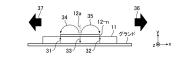
- FIG. 3 is an explanatory diagram showing an operation image of the microstrip antenna 12-n operating in the TM20 mode.
- the microstrip antenna 12-n receives an electromagnetic wave from the feeding unit 13-n via the feeding line 14-n, electric field vectors 31 and 32 are generated at both ends of the microstrip antenna 12-n.
- the electric field vector 31 and the electric field vector 32 are electric field vectors having the same phase, and the directions of the electric field vectors 31 and 32 are the + y direction.
- an electric field vector 33 having a phase opposite to that of the electric field vectors 31 and 32 is generated in the central portion of the microstrip antenna 12-n.
- the direction of the electric field vector 33 is the ⁇ y direction.
- an electric field vector 34 and an electric field vector 35 are generated as axis-symmetrical electric field vectors with respect to the central axis 12a of the microstrip antenna 12-n.
- the electromagnetic wave radiated in the radial direction 36 from each microstrip antenna 12-n is radiated to the outside through the opening 22.
- the electromagnetic wave radiated from each microstrip antenna 12-n in the radial direction 37 is reflected by the conductor wall 17.
- the electromagnetic wave after reflection by the conductor wall 17 is radiated to the outside from the opening 22. Since the distance D1 from the center of the microstrip antenna 12-1 to the conductor wall 17 is the distance represented by the equation (1), the electromagnetic wave after reflection by the conductor wall 17 and the microstrip antenna 12 are according to the principle of the mirror image.
- the electromagnetic wave radiated from the opening 22 to the outside is strengthened without the electromagnetic wave radiated from ⁇ n in the radial direction 36 weakening each other.
- the conductor walls 18 to 20 are provided to make the surrounding environment of the antenna device 1 less susceptible to the influence of electromagnetic waves, and to reflect the electromagnetic waves radiated from the microstrip antenna 12-n toward the opening 22 side. It is not provided. Therefore, the conductor walls 18 to 20 do not necessarily have to be provided in the antenna device 1.
- FIG. 4 is an explanatory diagram showing an electromagnetic field simulation result of the reflection characteristic in the antenna device 1 shown in FIG.
- the relative permittivity of the dielectric substrate 11 is 3.0
- the thickness of the dielectric substrate 11 is 0.026 ⁇
- the distance D1 is 3 ⁇ / 4.
- electromagnetic field simulation is performed assuming that electromagnetic waves are supplied to each of the microstrip antennas 12-1 to 12-4 from one feeding unit 41 via the feeding line 42. Is going.
- FIG. 5 is a plan view showing an antenna device 1 in which an electromagnetic field simulation of reflection characteristics is performed. In FIG.
- the horizontal axis represents the normalized frequency and the vertical axis represents the amplitude of the reflectance coefficient.
- the curve 51 shown in FIG. 4 shows the reflection characteristics of the antenna device 1, and there is a specific band of 1% or more in which the amplitude of the reflection coefficient is ⁇ 10 dB or less.
- FIG. 6 is an explanatory diagram showing an electromagnetic field simulation result of a radiation pattern at the center frequency of the antenna device 1 shown in FIG.
- FIG. 6A shows the electromagnetic field simulation result of the radiation pattern on the yz plane
- FIG. 6B shows the electromagnetic field simulation result of the radiation pattern on the xz plane.
- the horizontal axis represents an angle and the vertical axis represents a gain.
- the curve 52 shows the main polarization in the yz plane, and the main polarization in the yz plane represents the y-direction component.
- the curve 53 shows the cross-polarized wave in the yz plane, and the cross-polarized wave in the yz plane represents the x-direction component.
- the curve 54 shows the main polarization in the xz plane, and the main polarization in the xz plane represents the y-direction component.
- the curve 55 shows the cross-polarized wave in the xz plane, and the cross-polarized wave in the xz plane represents the x-direction component.
- the cross-polarized wave in the yz plane is ⁇ 20 dB or less with respect to the peak gain of the main polarized wave within the range of ⁇ 90 degrees.
- the crossed polarization in the xz plane is ⁇ 20 dB or less with respect to the peak gain of the main polarization within the range of ⁇ 90 degrees. Therefore, it can be seen that the antenna device 1 shown in FIG. 1 can radiate an electromagnetic wave in a direction parallel to the first plane 11a of the dielectric substrate 11.
- the dielectric substrate 11 having the first plane 11a and the second plane 11b and having the ground conductor provided on the second plane 11b, and the first in the dielectric substrate 11.
- the antenna device 1 is configured to include a plurality of microstrip antennas 12-1 to 12-4 which are arranged in a row on the plane 11a of 1 and operate in the TM20 mode. Therefore, the antenna device 1 can radiate electromagnetic waves in a direction parallel to the plane in which each microstrip antenna is arranged.
- the microstrip antennas 12-1 to 12-4 are shown to have a square shape. However, this is only an example, and the shape of the microstrip antennas 12-1 to 12-4 may be, for example, an ellipse or a polygon other than a square.
- the corner portions of the slits 15-1 to 15-4 and the slits 16-1 to 16-4 are shown to be at right angles. However, this is only an example, and each corner portion of the slits 15-1 to 15-4 and the slits 16-1 to 16-4 may be slightly rounded.
- the minute roundness at the corner portion is applied by, for example, etching or drilling.
- each of the microstrip antennas 12-1 to 12-4 radiates electromagnetic waves.
- Polarizers may be arranged in the + z direction of the microstrip antennas 12-1 to 12-4. By arranging the polarizer, the antenna device 1 shown in FIG. 1 can be operated as a circularly polarized wave antenna.
- the feeding unit 13-n may directly feed the electromagnetic wave to the microstrip antenna 12-n by using the RF connector.
- the feeding line 14-n, the slit 15-n and the slit 16-n are unnecessary.
- the electromagnetic wave may be supplied to the microstrip antenna 12-n by electromagnetic coupling to the microstrip antenna 12-n.
- Another dielectric substrate is arranged on the second plane 11b side of the dielectric substrate 11, and the electromagnetic wave propagates to the microstrip line formed on the other dielectric substrate, whereby the microstrip line and the microstrip line are formed.
- a configuration is conceivable in which the microstrip antenna 12-n is electromagnetically coupled.
- the intervals D2, D3, and D4 of the respective arrangements in the microstrip antennas 12-1 to 12-4 are the lengths of the wavelength ⁇ of the electromagnetic wave.
- FIG. 1 illustrates an example in which the antenna device 1 operates as a transmitting antenna. However, this is only an example, and the antenna device 1 can also operate as a receiving antenna.
- each of the microstrip antennas 12-1 to 12-4 and the feeding portions 13-1 to 13-4 are formed on the first flat surface 11a of the dielectric substrate 11 as conductor patterns. I am assuming what you are doing. However, this is only an example, and each of the microstrip antennas 12-1 to 12-4 and the feeding portions 13-1 to 13-4 is formed of a metal conductor, and a spacer is used instead of the dielectric substrate 11. You may.
- Embodiment 2 In the second embodiment, an antenna device 1 including a feeding line 14 for feeding electromagnetic waves to any one of the microstrip antennas 12-1 to 12-4 will be described.
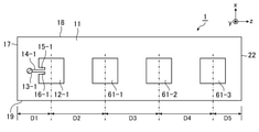
- FIG. 7 is a plan view showing the antenna device 1 according to the second embodiment.
- the microstrip antennas 61-1 to 61-3 are antennas that operate in the TM20 mode.
- the microstrip antennas 12-1 and the microstrip antennas 61-1 to 61-3 are arranged in a row on the first plane 11a of the dielectric substrate 11.
- the electromagnetic waves from the microstrip antennas 12-1 and the microstrip antennas 61-1 to 61-3 are in a direction parallel to the direction in which the microstrip antennas 12-1 and the microstrip antennas 61-1 to 61-3 are lined up in a row. Is radiated to.
- the distance between the arrangements of the microstrip antenna 12-1 and the microstrip antenna 61-1 is D2, and the distance between the arrangements of the microstrip antenna 61-1 and the microstrip antenna 61-2 is D3.
- the distance between the microstrip antenna 61-2 and the microstrip antenna 61-3 is D4. Since the feeding line is not connected to the microstrip antennas 61-1 to 61-3, the microstrip antennas 61-1 to 61-3 are not excited.
- the microstrip antennas 61-1 to 61-3 are interconnected with the microstrip antenna 12-1 between the elements. Therefore, the microstrip antennas 61-1 to 61-3 are excited by the excitation of the microstrip antenna 12-1. When the microstrip antennas 61-1 to 61-3 are excited, they emit electromagnetic waves in a direction parallel to the first plane 11a.
- the intervals between the arrangements are D2, D3, and D4, and the intervals D2, D3, and D4 may be the length of the wavelength ⁇ of the electromagnetic wave, but the wavelength ⁇ of the electromagnetic wave. It may be shorter than the length. If the intervals D2, D3, and D4 are shorter than the length of the wavelength ⁇ of the electromagnetic wave, the mutual coupling between the elements of the microstrip antenna 12-1 and the microstrip antennas 61-1 to 61-3 can be strengthened.
- the microstrip antenna 12-1 is arranged at the position farthest from the opening 22. ..
- the microstrip antenna 12-1 may be arranged at a position other than the position farthest from the opening 22, for example, as shown in FIG.
- FIG. 8 is a plan view showing another antenna device 1 according to the second embodiment.
- the microstrip antenna 61-1 is arranged at a position other than the position farthest from the opening 22. Has been done.
- the microstrip antenna 12-1 is located at the second farthest position from the opening 22.
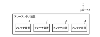
- Embodiment 3 an array antenna device in which a plurality of antenna devices 1 shown in FIGS. 1, 7 or 8 are arranged on the same plane will be described.
- FIG. 9 is a plan view showing the array antenna device according to the third embodiment.
- a plurality of antenna devices 1 are arranged in a row on the same plane.
- a plurality of antenna devices 1 may be arranged so that the radiation directions of the electromagnetic waves radiated from each of the plurality of antenna devices 1 are the same, or the electromagnetic waves radiated from each of the plurality of antenna devices 1 may be arranged.
- a plurality of antenna devices 1 may be arranged so that the radial directions are different.
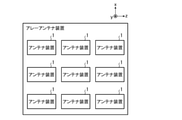
- FIG. 10 is a plan view showing another array antenna device according to the third embodiment.
- any combination of the embodiments can be freely combined, any component of the embodiment can be modified, or any component can be omitted in each embodiment.
- the present disclosure is suitable for an antenna device and an array antenna device having a plurality of microstrip antennas.
- 1 antenna device 11 dielectric substrate, 11a first plane, 11b second plane, 12-1 to 12-4 microstrip antenna, 12a central axis, 13-1 to 13-4 feeding part, 14-1 to 14-4 power supply line, 15-1 to 15-4 slit, 16-1 to 16-4 slit, 17 to 21 conductor wall, 22 opening, 31 to 35 electric field vector, 36, 37 radial direction, 41 power supply part, 42 power supply line, 51-55 curve, 61-1-61-3 microstrip antenna.
Landscapes
- Waveguide Aerials (AREA)
- Variable-Direction Aerials And Aerial Arrays (AREA)
Abstract
第1の平面(11a)及び第2の平面(11b)を有しており、第2の平面(11b)に接地導体が施されている誘電体基板(11)と、誘電体基板(11)における第1の平面(11a)に一列に配置されており、TM20モードで動作する複数のマイクロストリップアンテナ(12-1)~(12-4)とを備えるように、アンテナ装置(1)を構成した。
Description
本開示は、複数のマイクロストリップアンテナを備えるアンテナ装置及びアレーアンテナ装置に関するものである。
以下の非特許文献1には、複数のマイクロストリップアンテナを備えるアンテナ装置が開示されている。当該マイクロストリップアンテナは、TM10モードで動作するアンテナである。それぞれのマイクロストリップアンテナが配置されている平面と直交する方向が0度、当該平面と平行な方向が90度であるとすると、それぞれのマイクロストリップアンテナからの電磁波の放射方向は、30~45度の方向である。
G. R. DeJean and M. M. Tentzeris, "A New High-Gain Microstrip Yagi Array Antenna With a High Front-to-Back (F/B) Ratio for WLAN and Millimeter-Wave Applications," IEEE Trans. on Antennas and Propagat., Vol. 55, No. 2, 2007.
非特許文献1に開示されているアンテナ装置では、それぞれのマイクロストリップアンテナが配置されている平面と平行な方向に電磁波を放射することができないという課題があった。
本開示は、上記のような課題を解決するためになされたもので、それぞれのマイクロストリップアンテナが配置されている平面と平行な方向に電磁波を放射することができるアンテナ装置を得ることを目的とする。
本開示に係るアンテナ装置は、第1の平面及び第2の平面を有しており、第2の平面に接地導体が施されている誘電体基板と、誘電体基板における第1の平面に一列に配置されており、TM20モードで動作する複数のマイクロストリップアンテナとを備えるものである。
本開示によれば、それぞれのマイクロストリップアンテナが配置されている平面と平行な方向に電磁波を放射することができる。
以下、本開示をより詳細に説明するために、本開示を実施するための形態について、添付の図面に従って説明する。
実施の形態1.
図1は、実施の形態1に係るアンテナ装置1を示す平面図である。
図2は、図1に示すアンテナ装置1におけるC1-C2断面を示す断面図である。
図1に示すアンテナ装置1は、x-y-zの座標軸によって表される3次元空間において、xz面と平行な平面に配置されている。
誘電体基板11は、第1の平面11a及び第2の平面11bを有している。
誘電体基板11の第2の平面11bには、接地導体が施されている。
誘電体基板11の第1の平面11aには、4つのマイクロストリップアンテナ12-1~12-4が配置されている。
図1に示すアンテナ装置1は、4つのマイクロストリップアンテナ12-1~12-4が配置されている。しかし、これは一例に過ぎず、2つ以上のマイクロストリップアンテナ12が配置されていればよい。
以下、マイクロストリップアンテナ12-1~12-4を区別しない場合は、マイクロストリップアンテナ12のように表記する。
図1は、実施の形態1に係るアンテナ装置1を示す平面図である。
図2は、図1に示すアンテナ装置1におけるC1-C2断面を示す断面図である。
図1に示すアンテナ装置1は、x-y-zの座標軸によって表される3次元空間において、xz面と平行な平面に配置されている。
誘電体基板11は、第1の平面11a及び第2の平面11bを有している。
誘電体基板11の第2の平面11bには、接地導体が施されている。
誘電体基板11の第1の平面11aには、4つのマイクロストリップアンテナ12-1~12-4が配置されている。
図1に示すアンテナ装置1は、4つのマイクロストリップアンテナ12-1~12-4が配置されている。しかし、これは一例に過ぎず、2つ以上のマイクロストリップアンテナ12が配置されていればよい。
以下、マイクロストリップアンテナ12-1~12-4を区別しない場合は、マイクロストリップアンテナ12のように表記する。
マイクロストリップアンテナ12-1~12-4は、誘電体基板11における第1の平面11aに一列に配置されている。
マイクロストリップアンテナ12-1~12-4は、TM20モードで動作するアンテナであり、第1の平面11aと平行な方向に電磁波を放射する。
マイクロストリップアンテナ12からの電磁波は、マイクロストリップアンテナ12-1~12-4が一列に並んでいる方向と平行な方向に放射される。
マイクロストリップアンテナ12-1~12-4におけるそれぞれの配置の間隔D2,D3,D4は、電磁波の波長λの長さである。
間隔D2,D3,D4は、電磁波の波長λの長さと厳密に一致しているものに限るものではなく、実用上問題のない範囲で波長λの長さと異なっていてもよい。
マイクロストリップアンテナ12-1~12-4は、TM20モードで動作するアンテナであり、第1の平面11aと平行な方向に電磁波を放射する。
マイクロストリップアンテナ12からの電磁波は、マイクロストリップアンテナ12-1~12-4が一列に並んでいる方向と平行な方向に放射される。
マイクロストリップアンテナ12-1~12-4におけるそれぞれの配置の間隔D2,D3,D4は、電磁波の波長λの長さである。
間隔D2,D3,D4は、電磁波の波長λの長さと厳密に一致しているものに限るものではなく、実用上問題のない範囲で波長λの長さと異なっていてもよい。
給電部13-n(n=1,2,3,4)は、給電線路14-nを介して、マイクロストリップアンテナ12-nと接続されている。
給電部13-nは、給電線路14-nを介して、マイクロストリップアンテナ12-nに電磁波を給電する。
給電線路14-nの一端は、給電部13-nと接続され、給電線路14-nの他端は、マイクロストリップアンテナ12-nと接続されている。
給電線路14-nは、給電部13-nから出力された電磁波が伝搬する。
給電部13-nは、給電線路14-nを介して、マイクロストリップアンテナ12-nに電磁波を給電する。
給電線路14-nの一端は、給電部13-nと接続され、給電線路14-nの他端は、マイクロストリップアンテナ12-nと接続されている。
給電線路14-nは、給電部13-nから出力された電磁波が伝搬する。
スリット15-nは、マイクロストリップアンテナ12-nと給電線路14-nとの間の隙間である。
スリット16-nは、マイクロストリップアンテナ12-nと給電線路14-nとの間の隙間である。
スリット16-nは、マイクロストリップアンテナ12-nと給電線路14-nとの間の隙間である。
導体壁17は、マイクロストリップアンテナ12-1~12-4が一列に並んでいる方向に配置されており、マイクロストリップアンテナ12-1~12-4のそれぞれから放射された電磁波を反射させる。
導体壁17が配置されている位置は、マイクロストリップアンテナ12-1~12-4のうち、端部に配置されているマイクロストリップアンテナ12-1の中心から、波長λの4分の1の長さと、波長λの2分の1の長さの整数倍の長さとの和の距離だけ離れている位置である。
即ち、マイクロストリップアンテナ12-1の中心から導体壁17までの距離D1は、以下の式(1)のように表される。
 式(1)において、mは、1以上の整数である。
導体壁17が配置されている位置は、マイクロストリップアンテナ12-1~12-4のうち、端部に配置されているマイクロストリップアンテナ12-1の中心から、波長λの4分の1の長さと、波長λの2分の1の長さの整数倍の長さとの和の距離だけ離れている位置である。
即ち、マイクロストリップアンテナ12-1の中心から導体壁17までの距離D1は、以下の式(1)のように表される。
導体壁18は、マイクロストリップアンテナ12-1~12-4のそれぞれから放射された電磁波が、x軸と平行な方向である+x方向に漏れ出るのを防ぐために設けられている。
導体壁19は、マイクロストリップアンテナ12-1~12-4のそれぞれから放射された電磁波が、x軸と平行な方向である-x方向に漏れ出るのを防ぐために設けられている。
導体壁20は、マイクロストリップアンテナ12-1~12-4のそれぞれから放射された電磁波が、y軸と平行な方向である+y方向に漏れ出るのを防ぐために設けられている。
導体壁21は、マイクロストリップアンテナ12-1~12-4のそれぞれをパッチアンテナとして動作させるために設けられている。
導体壁17~21によって、誘電体基板11及びマイクロストリップアンテナ12-1~12-4を含む空間が形成されている。
開口部22は、アンテナ装置1の外部空間との境界面であり、開口部22から、マイクロストリップアンテナ12-1~12-4のそれぞれから放射された電磁波が外部に放射される。
D5は、マイクロストリップアンテナ12-4の中心から開口部22までの距離であり、距離D5は、どのような距離でもよい。
導体壁19は、マイクロストリップアンテナ12-1~12-4のそれぞれから放射された電磁波が、x軸と平行な方向である-x方向に漏れ出るのを防ぐために設けられている。
導体壁20は、マイクロストリップアンテナ12-1~12-4のそれぞれから放射された電磁波が、y軸と平行な方向である+y方向に漏れ出るのを防ぐために設けられている。
導体壁21は、マイクロストリップアンテナ12-1~12-4のそれぞれをパッチアンテナとして動作させるために設けられている。
導体壁17~21によって、誘電体基板11及びマイクロストリップアンテナ12-1~12-4を含む空間が形成されている。
開口部22は、アンテナ装置1の外部空間との境界面であり、開口部22から、マイクロストリップアンテナ12-1~12-4のそれぞれから放射された電磁波が外部に放射される。
D5は、マイクロストリップアンテナ12-4の中心から開口部22までの距離であり、距離D5は、どのような距離でもよい。
次に、図1に示すアンテナ装置1の動作について説明する。
ここでは、アンテナ装置1が、送信アンテナとして動作する例を説明する。
給電部13-n(n=1,2,3,4)は、給電線路14-nを介して、マイクロストリップアンテナ12-nに電磁波を給電する。
即ち、給電部13-nから給電された電磁波は、給電線路14-nをz軸と平行な方向である+z方向に伝搬し、マイクロストリップアンテナ12-nに到達する。
マイクロストリップアンテナ12-nに到達した電磁波のうち、一部の電磁波は、マイクロストリップアンテナ12-nから放射される。
マイクロストリップアンテナ12-nから放射されていない電磁波は、給電線路14-nを介して、給電部13-nに反射波として戻る。
なお、給電部13-nから給電された電磁波の一部の電力は、給電線路14-n、あるいは、マイクロストリップアンテナ12-nにおいて、熱損となる。
ここでは、アンテナ装置1が、送信アンテナとして動作する例を説明する。
給電部13-n(n=1,2,3,4)は、給電線路14-nを介して、マイクロストリップアンテナ12-nに電磁波を給電する。
即ち、給電部13-nから給電された電磁波は、給電線路14-nをz軸と平行な方向である+z方向に伝搬し、マイクロストリップアンテナ12-nに到達する。
マイクロストリップアンテナ12-nに到達した電磁波のうち、一部の電磁波は、マイクロストリップアンテナ12-nから放射される。
マイクロストリップアンテナ12-nから放射されていない電磁波は、給電線路14-nを介して、給電部13-nに反射波として戻る。
なお、給電部13-nから給電された電磁波の一部の電力は、給電線路14-n、あるいは、マイクロストリップアンテナ12-nにおいて、熱損となる。
図1に示すアンテナ装置1では、スリット15-n及びスリット16-nが設けられている。
スリット15-nのz方向の長さ及びスリット16-nのz方向の長さのそれぞれを調整することによって、アンテナ装置1の入力インピーダンスの実部である抵抗値を調整することができる。
また、スリット15-nのx方向の長さ及びスリット16-nのx方向の長さのそれぞれを調整することによって、アンテナ装置1の入力インピーダンスの虚部であるリアクタンス値を調整することができる。
したがって、図1に示すアンテナ装置1では、スリット15-n及びスリット16-nにおけるそれぞれのサイズを調整することによって、給電部13-nに戻る反射波を低減することができる。サイズの調整は、x方向の寸法と、z方向の寸法との調整を意味する。
スリット15-nのz方向の長さ及びスリット16-nのz方向の長さのそれぞれを調整することによって、アンテナ装置1の入力インピーダンスの実部である抵抗値を調整することができる。
また、スリット15-nのx方向の長さ及びスリット16-nのx方向の長さのそれぞれを調整することによって、アンテナ装置1の入力インピーダンスの虚部であるリアクタンス値を調整することができる。
したがって、図1に示すアンテナ装置1では、スリット15-n及びスリット16-nにおけるそれぞれのサイズを調整することによって、給電部13-nに戻る反射波を低減することができる。サイズの調整は、x方向の寸法と、z方向の寸法との調整を意味する。
マイクロストリップアンテナ12-nは、TM20モードで動作するアンテナであり、給電部13-nから、給電線路14-nを介して、電磁波の給電を受けると、第1の平面11aと平行な方向に電磁波を放射する。
即ち、マイクロストリップアンテナ12-nは、+z方向と-z方向とに電磁波を放射する。
即ち、マイクロストリップアンテナ12-nは、+z方向と-z方向とに電磁波を放射する。
図3は、TM20モードで動作するマイクロストリップアンテナ12-nの動作イメージを示す説明図である。
マイクロストリップアンテナ12-nは、給電部13-nから、給電線路14-nを介して、電磁波の給電を受けると、マイクロストリップアンテナ12-nの両端に電界ベクトル31,32が生じる。
電界ベクトル31と電界ベクトル32とは、同相の電界ベクトルであり、電界ベクトル31,32の向きは、+y方向である。
また、マイクロストリップアンテナ12-nの中央部に、電界ベクトル31,32と逆相の電界ベクトル33が生じる。電界ベクトル33の向きは、-y方向である。
さらに、マイクロストリップアンテナ12-nの上部である+y方向には、マイクロストリップアンテナ12-nの中心軸12aに関して、軸対称の電界ベクトルとして、電界ベクトル34と電界ベクトル35とが生じる。
マイクロストリップアンテナ12-nは、給電部13-nから、給電線路14-nを介して、電磁波の給電を受けると、マイクロストリップアンテナ12-nの両端に電界ベクトル31,32が生じる。
電界ベクトル31と電界ベクトル32とは、同相の電界ベクトルであり、電界ベクトル31,32の向きは、+y方向である。
また、マイクロストリップアンテナ12-nの中央部に、電界ベクトル31,32と逆相の電界ベクトル33が生じる。電界ベクトル33の向きは、-y方向である。
さらに、マイクロストリップアンテナ12-nの上部である+y方向には、マイクロストリップアンテナ12-nの中心軸12aに関して、軸対称の電界ベクトルとして、電界ベクトル34と電界ベクトル35とが生じる。
電界ベクトル31~35が生じる結果、マイクロストリップアンテナ12-nから、アンテナ正面方向である+y方向には電磁波が放射されず、+x方向と-x方向とに電磁波が放射される。
図3において、36は、マイクロストリップアンテナ12-nからの電磁波の放射方向であり、放射方向36は、+x方向である。
37は、マイクロストリップアンテナ12-nからの電磁波の放射方向であり、放射方向37は、-x方向である。
図3において、36は、マイクロストリップアンテナ12-nからの電磁波の放射方向であり、放射方向36は、+x方向である。
37は、マイクロストリップアンテナ12-nからの電磁波の放射方向であり、放射方向37は、-x方向である。
それぞれのマイクロストリップアンテナ12-nから、放射方向36に放射された電磁波は、開口部22から外部に放射される。
それぞれのマイクロストリップアンテナ12-nから、放射方向37に放射された電磁波は、導体壁17に反射される。
導体壁17による反射後の電磁波は、開口部22から外部に放射される。
マイクロストリップアンテナ12-1の中心から導体壁17までの距離D1が、式(1)によって表される距離であるため、鏡像の原理によって、導体壁17による反射後の電磁波と、マイクロストリップアンテナ12-nから放射方向36に放射された電磁波とが、互いに弱め合う等の影響を及ぼすことなく、開口部22から外部に放射される電磁波が強められる。開口部22から電磁波が外部に放射されることにより、放射方向36にビームが形成される。
導体壁18~20は、アンテナ装置1の周囲の環境に電磁波の影響を受け難くするために設けられており、マイクロストリップアンテナ12-nから放射された電磁波を開口部22側に反射させるために設けられているものではない。したがって、導体壁18~20は、必ずしも、アンテナ装置1に設けられていなくてもよい。
それぞれのマイクロストリップアンテナ12-nから、放射方向37に放射された電磁波は、導体壁17に反射される。
導体壁17による反射後の電磁波は、開口部22から外部に放射される。
マイクロストリップアンテナ12-1の中心から導体壁17までの距離D1が、式(1)によって表される距離であるため、鏡像の原理によって、導体壁17による反射後の電磁波と、マイクロストリップアンテナ12-nから放射方向36に放射された電磁波とが、互いに弱め合う等の影響を及ぼすことなく、開口部22から外部に放射される電磁波が強められる。開口部22から電磁波が外部に放射されることにより、放射方向36にビームが形成される。
導体壁18~20は、アンテナ装置1の周囲の環境に電磁波の影響を受け難くするために設けられており、マイクロストリップアンテナ12-nから放射された電磁波を開口部22側に反射させるために設けられているものではない。したがって、導体壁18~20は、必ずしも、アンテナ装置1に設けられていなくてもよい。
次に、図1に示すアンテナ装置1の有用性を示すために、アンテナ装置1の特性を説明する。
図4は、図1に示すアンテナ装置1における反射特性の電磁界シミュレーション結果を示す説明図である。
反射特性の電磁界シミュレーションでは、誘電体基板11の比誘電率が3.0、誘電体基板11の厚さが0.026λ、距離D1が3λ/4としている。
また、マイクロストリップアンテナ12-1~12-4のそれぞれには、図5に示すように、1つの給電部41から、給電線路42を介して、電磁波が給電されるものとして、電磁界シミュレーションを行っている。図5は、反射特性の電磁界シミュレーションが行われたアンテナ装置1を示す平面図である。
図4において、横軸は、正規化周波数を示し、縦軸は、反射係数の振幅を示している。
図4に示す曲線51は、アンテナ装置1の反射特性を示しており、反射係数の振幅が-10dB以下となる比帯域が1%以上存在している。
図4は、図1に示すアンテナ装置1における反射特性の電磁界シミュレーション結果を示す説明図である。
反射特性の電磁界シミュレーションでは、誘電体基板11の比誘電率が3.0、誘電体基板11の厚さが0.026λ、距離D1が3λ/4としている。
また、マイクロストリップアンテナ12-1~12-4のそれぞれには、図5に示すように、1つの給電部41から、給電線路42を介して、電磁波が給電されるものとして、電磁界シミュレーションを行っている。図5は、反射特性の電磁界シミュレーションが行われたアンテナ装置1を示す平面図である。
図4において、横軸は、正規化周波数を示し、縦軸は、反射係数の振幅を示している。
図4に示す曲線51は、アンテナ装置1の反射特性を示しており、反射係数の振幅が-10dB以下となる比帯域が1%以上存在している。
図6は、図1に示すアンテナ装置1の中心周波数における放射パターンの電磁界シミュレーション結果を示す説明図である。
図6Aは、yz面における放射パターンの電磁界シミュレーション結果を示し、図6Bは、xz面における放射パターンの電磁界シミュレーション結果を示している。
図6A及び図6Bにおいて、横軸は、角度を示し、縦軸は、利得を示している。
曲線52は、yz面における主偏波を示しており、yz面における主偏波は、y方向成分を表している。
曲線53は、yz面における交差偏波を示しており、yz面における交差偏波は、x方向成分を表している。
曲線54は、xz面における主偏波を示しており、xz面における主偏波は、y方向成分を表している。
曲線55は、xz面における交差偏波を示しており、xz面における交差偏波は、x方向成分を表している。
図6Aは、yz面における放射パターンの電磁界シミュレーション結果を示し、図6Bは、xz面における放射パターンの電磁界シミュレーション結果を示している。
図6A及び図6Bにおいて、横軸は、角度を示し、縦軸は、利得を示している。
曲線52は、yz面における主偏波を示しており、yz面における主偏波は、y方向成分を表している。
曲線53は、yz面における交差偏波を示しており、yz面における交差偏波は、x方向成分を表している。
曲線54は、xz面における主偏波を示しており、xz面における主偏波は、y方向成分を表している。
曲線55は、xz面における交差偏波を示しており、xz面における交差偏波は、x方向成分を表している。
図6Aの曲線52が示すように、yz面における主偏波は、誘電体基板11の第1の平面11aと平行な方向である+z方向、即ち、Angle=0(degree)を指向していることが分かる。
図6Aの曲線53が示すように、yz面における交差偏波は、±90度の範囲内で主偏波のピーク利得に対して、-20dB以下である。
図6Bの曲線54が示すように、xz面における主偏波は、誘電体基板11の第1の平面11aと平行な方向である+z方向、即ち、Angle=0(degree)を指向していることが分かる。
図6Bの曲線55が示すように、xz面における交差偏波は、±90度の範囲内で主偏波のピーク利得に対して、-20dB以下である。
したがって、図1に示すアンテナ装置1は、誘電体基板11の第1の平面11aと平行な方向に電磁波を放射できることが分かる。
図6Aの曲線53が示すように、yz面における交差偏波は、±90度の範囲内で主偏波のピーク利得に対して、-20dB以下である。
図6Bの曲線54が示すように、xz面における主偏波は、誘電体基板11の第1の平面11aと平行な方向である+z方向、即ち、Angle=0(degree)を指向していることが分かる。
図6Bの曲線55が示すように、xz面における交差偏波は、±90度の範囲内で主偏波のピーク利得に対して、-20dB以下である。
したがって、図1に示すアンテナ装置1は、誘電体基板11の第1の平面11aと平行な方向に電磁波を放射できることが分かる。
以上の実施の形態1では、第1の平面11a及び第2の平面11bを有しており、第2の平面11bに接地導体が施されている誘電体基板11と、誘電体基板11における第1の平面11aに一列に配置されており、TM20モードで動作する複数のマイクロストリップアンテナ12-1~12-4とを備えるように、アンテナ装置1を構成した。したがって、アンテナ装置1は、それぞれのマイクロストリップアンテナが配置されている平面と平行な方向に電磁波を放射することができる。
図1に示すアンテナ装置1では、マイクロストリップアンテナ12-1~12-4の形状が方形であるものを示している。しかし、これは一例に過ぎず、マイクロストリップアンテナ12-1~12-4の形状が、例えば、楕円形、又は、方形以外の多角形であってもよい。
図1に示すアンテナ装置1では、スリット15-1~15-4及びスリット16-1~16-4におけるそれぞれのコーナー部分が直角であるものを示している。しかし、これは一例に過ぎず、スリット15-1~15-4及びスリット16--1~16-4におけるそれぞれのコーナー部分に、微小の丸みが施されていてもよい。コーナー部分における微小の丸みは、例えば、エッチング加工、又は、ドリル加工によって施される。
図1に示すアンテナ装置1では、マイクロストリップアンテナ12-1~12-4のそれぞれが電磁波を放射している。マイクロストリップアンテナ12-1~12-4の+z方向に、ポラライザが配置されていてもよい。ポラライザが配置されることによって、図1に示すアンテナ装置1を円偏波アンテナとして動作させることが可能である。
図1に示すアンテナ装置1では、給電部13-n(n=1,2,3,4)が、給電線路14-nを介して、マイクロストリップアンテナ12-nに電磁波を給電している。しかし、これは一例に過ぎず、例えば、給電部13-nが、RFコネクタを用いて、マイクロストリップアンテナ12-nに電磁波を直接給電するようにしてもよい。この場合、給電線路14-n、スリット15-n及びスリット16-nは、不要である。
また、マイクロストリップアンテナ12-nに対する電磁結合によって、マイクロストリップアンテナ12-nに電磁波を給電するようにしてもよい。
即ち、誘電体基板11における第2の平面11b側に、別の誘電体基板を配置し、別の誘電体基板に形成されているマイクロストリップ線路に電磁波が伝搬することによって、当該マイクロストリップ線路と、マイクロストリップアンテナ12-nとが電磁結合する構成が考えられる。
また、マイクロストリップアンテナ12-nに対する電磁結合によって、マイクロストリップアンテナ12-nに電磁波を給電するようにしてもよい。
即ち、誘電体基板11における第2の平面11b側に、別の誘電体基板を配置し、別の誘電体基板に形成されているマイクロストリップ線路に電磁波が伝搬することによって、当該マイクロストリップ線路と、マイクロストリップアンテナ12-nとが電磁結合する構成が考えられる。
図1に示すアンテナ装置1では、マイクロストリップアンテナ12-1~12-4におけるそれぞれの配置の間隔D2,D3,D4が、電磁波の波長λの長さである。しかし、これは一例に過ぎず、隣り合う2つのマイクロストリップアンテナ12同士が物理的に干渉しなければよく、それぞれの配置の間隔D2,D3,D4が、電磁波の波長λの長さに限るものではない。
図1では、アンテナ装置1が、送信アンテナとして動作する例を説明している。しかし、これは一例に過ぎず、アンテナ装置1が、受信アンテナとして動作することもできる。
図1に示すアンテナ装置1では、マイクロストリップアンテナ12-1~12-4及び給電部13-1~13-4のそれぞれが、導体パターンとして、誘電体基板11の第1の平面11aに形成されているものを想定している。しかし、これは一例に過ぎず、マイクロストリップアンテナ12-1~12-4及び給電部13-1~13-4のそれぞれを金属導体によって形成し、誘電体基板11の代わりにスペーサを用いるようにしてもよい。
実施の形態2.
実施の形態2では、マイクロストリップアンテナ12-1~12-4のうち、いずれか1つのマイクロストリップアンテナ12に電磁波を給電するための給電線路14を備えるアンテナ装置1について説明する。
実施の形態2では、マイクロストリップアンテナ12-1~12-4のうち、いずれか1つのマイクロストリップアンテナ12に電磁波を給電するための給電線路14を備えるアンテナ装置1について説明する。
図7は、実施の形態2に係るアンテナ装置1を示す平面図である。図7において、図1と同一符号は同一又は相当部分を示すので説明を省略する。
マイクロストリップアンテナ61-1~61-3は、TM20モードで動作するアンテナである。
マイクロストリップアンテナ12-1及びマイクロストリップアンテナ61-1~61-3は、誘電体基板11における第1の平面11aに一列に配置されている。
マイクロストリップアンテナ12-1及びマイクロストリップアンテナ61-1~61-3からの電磁波は、マイクロストリップアンテナ12-1及びマイクロストリップアンテナ61-1~61-3が一列に並んでいる方向と平行な方向に放射される。
マイクロストリップアンテナ12-1とマイクロストリップアンテナ61-1との配置の間隔はD2であり、マイクロストリップアンテナ61-1とマイクロストリップアンテナ61-2との配置の間隔はD3である。また、マイクロストリップアンテナ61-2とマイクロストリップアンテナ61-3との配置の間隔はD4である。
マイクロストリップアンテナ61-1~61-3には、給電線路が接続されていないため、マイクロストリップアンテナ61-1~61-3は、励振しない。
マイクロストリップアンテナ61-1~61-3は、マイクロストリップアンテナ12-1と素子間相互結合される。したがって、マイクロストリップアンテナ61-1~61-3は、マイクロストリップアンテナ12-1が励振することによって励起される。
マイクロストリップアンテナ61-1~61-3は、励起されることによって、第1の平面11aと平行な方向に電磁波を放射する。
マイクロストリップアンテナ61-1~61-3は、TM20モードで動作するアンテナである。
マイクロストリップアンテナ12-1及びマイクロストリップアンテナ61-1~61-3は、誘電体基板11における第1の平面11aに一列に配置されている。
マイクロストリップアンテナ12-1及びマイクロストリップアンテナ61-1~61-3からの電磁波は、マイクロストリップアンテナ12-1及びマイクロストリップアンテナ61-1~61-3が一列に並んでいる方向と平行な方向に放射される。
マイクロストリップアンテナ12-1とマイクロストリップアンテナ61-1との配置の間隔はD2であり、マイクロストリップアンテナ61-1とマイクロストリップアンテナ61-2との配置の間隔はD3である。また、マイクロストリップアンテナ61-2とマイクロストリップアンテナ61-3との配置の間隔はD4である。
マイクロストリップアンテナ61-1~61-3には、給電線路が接続されていないため、マイクロストリップアンテナ61-1~61-3は、励振しない。
マイクロストリップアンテナ61-1~61-3は、マイクロストリップアンテナ12-1と素子間相互結合される。したがって、マイクロストリップアンテナ61-1~61-3は、マイクロストリップアンテナ12-1が励振することによって励起される。
マイクロストリップアンテナ61-1~61-3は、励起されることによって、第1の平面11aと平行な方向に電磁波を放射する。
図7に示すアンテナ装置1では、それぞれの配置の間隔がD2,D3,D4であり、間隔D2,D3,D4は、電磁波の波長λの長さであってもよいが、電磁波の波長λの長さよりも短くてもよい。間隔D2,D3,D4が電磁波の波長λの長さよりも短ければ、マイクロストリップアンテナ12-1とマイクロストリップアンテナ61-1~61-3との素子間相互結合を強めることができる。
図7に示すアンテナ装置1では、マイクロストリップアンテナ12-1及びマイクロストリップアンテナ61-1~61-3の中で、マイクロストリップアンテナ12-1が、開口部22から最も遠い位置に配置されている。しかし、これは一例に過ぎず、マイクロストリップアンテナ12-1は、例えば、図8に示すように、開口部22から最も遠い位置以外の位置に配置されていてもよい。
図8は、実施の形態2に係る他のアンテナ装置1を示す平面図である。
図8に示すアンテナ装置1では、マイクロストリップアンテナ12-1及びマイクロストリップアンテナ61-1~61-3の中で、マイクロストリップアンテナ61-1が、開口部22から最も遠い位置以外の位置に配置されている。マイクロストリップアンテナ12-1は、開口部22から、2番目に遠い位置に配置されている。
図8は、実施の形態2に係る他のアンテナ装置1を示す平面図である。
図8に示すアンテナ装置1では、マイクロストリップアンテナ12-1及びマイクロストリップアンテナ61-1~61-3の中で、マイクロストリップアンテナ61-1が、開口部22から最も遠い位置以外の位置に配置されている。マイクロストリップアンテナ12-1は、開口部22から、2番目に遠い位置に配置されている。
実施の形態3.
実施の形態3では、図1、図7又は図8に示すアンテナ装置1が同一の平面上に複数配置されているアレーアンテナ装置について説明する。
実施の形態3では、図1、図7又は図8に示すアンテナ装置1が同一の平面上に複数配置されているアレーアンテナ装置について説明する。
図9は、実施の形態3に係るアレーアンテナ装置を示す平面図である。
図9に示すアレーアンテナ装置では、複数のアンテナ装置1が同一の平面上に一列に配置されている。
複数のアンテナ装置1のそれぞれから放射される電磁波の放射方向が同一方向になるように、複数のアンテナ装置1が配置されていてもよいし、複数のアンテナ装置1のそれぞれから放射される電磁波の放射方向が異なる方向になるように、複数のアンテナ装置1が配置されていてもよい。
図9に示すアレーアンテナ装置では、複数のアンテナ装置1が同一の平面上に一列に配置されている。
複数のアンテナ装置1のそれぞれから放射される電磁波の放射方向が同一方向になるように、複数のアンテナ装置1が配置されていてもよいし、複数のアンテナ装置1のそれぞれから放射される電磁波の放射方向が異なる方向になるように、複数のアンテナ装置1が配置されていてもよい。
図9に示すアレーアンテナ装置では、複数のアンテナ装置1が同一の平面上に一列に配置されている。しかし、これは一例に過ぎず、例えば、図10に示すように、複数のアンテナ装置1が同一の平面上に格子状に配置されていてもよい。
図10は、実施の形態3に係る他のアレーアンテナ装置を示す平面図である。
図10は、実施の形態3に係る他のアレーアンテナ装置を示す平面図である。
なお、本開示は、各実施の形態の自由な組み合わせ、あるいは各実施の形態の任意の構成要素の変形、もしくは各実施の形態において任意の構成要素の省略が可能である。
本開示は、複数のマイクロストリップアンテナを備えるアンテナ装置及びアレーアンテナ装置に適している。
1 アンテナ装置、11 誘電体基板、11a 第1の平面、11b 第2の平面、12-1~12-4 マイクロストリップアンテナ、12a 中心軸、13-1~13-4 給電部、14-1~14-4 給電線路、15-1~15-4 スリット、16-1~16-4 スリット、17~21 導体壁、22 開口部、31~35 電界ベクトル、36,37 放射方向、41 給電部、42 給電線路、51~55 曲線、61-1~61-3 マイクロストリップアンテナ。
Claims (5)
- 第1の平面及び第2の平面を有しており、前記第2の平面に接地導体が施されている誘電体基板と、
前記誘電体基板における前記第1の平面に一列に配置されており、TM20モードで動作する複数のマイクロストリップアンテナと
を備えたアンテナ装置。 - 前記複数のマイクロストリップアンテナが一列に並んでいる方向に配置されている導体壁を備え、
前記導体壁が配置されている位置は、
前記複数のマイクロストリップアンテナのうち、端部に配置されているマイクロストリップアンテナの中心から、前記波長の4分の1の長さと、前記波長の2分の1の長さの整数倍の長さとの和の距離だけ離れている位置であることを特徴とする請求項1記載のアンテナ装置。 - それぞれのマイクロストリップアンテナに電磁波を給電するための複数の給電線路を備えたことを特徴とする請求項1記載のアンテナ装置。
- 前記複数のマイクロストリップアンテナのうち、いずれか1つのマイクロストリップアンテナに電磁波を給電するための給電線路を備えたことを特徴とする請求項1記載のアンテナ装置。
- 請求項1から請求項4のうちのいずれか1項記載のアンテナ装置が同一の平面上に複数配置されていることを特徴とするアレーアンテナ装置。
Priority Applications (2)
| Application Number | Priority Date | Filing Date | Title |
|---|---|---|---|
| PCT/JP2020/027913 WO2022014053A1 (ja) | 2020-07-17 | 2020-07-17 | アンテナ装置及びアレーアンテナ装置 |
| JP2021562063A JP7106019B2 (ja) | 2020-07-17 | 2020-07-17 | アンテナ装置及びアレーアンテナ装置 |
Applications Claiming Priority (1)
| Application Number | Priority Date | Filing Date | Title |
|---|---|---|---|
| PCT/JP2020/027913 WO2022014053A1 (ja) | 2020-07-17 | 2020-07-17 | アンテナ装置及びアレーアンテナ装置 |
Publications (1)
| Publication Number | Publication Date |
|---|---|
| WO2022014053A1 true WO2022014053A1 (ja) | 2022-01-20 |
Family
ID=79554615
Family Applications (1)
| Application Number | Title | Priority Date | Filing Date |
|---|---|---|---|
| PCT/JP2020/027913 Ceased WO2022014053A1 (ja) | 2020-07-17 | 2020-07-17 | アンテナ装置及びアレーアンテナ装置 |
Country Status (2)
| Country | Link |
|---|---|
| JP (1) | JP7106019B2 (ja) |
| WO (1) | WO2022014053A1 (ja) |
Citations (6)
| Publication number | Priority date | Publication date | Assignee | Title |
|---|---|---|---|---|
| JPH01248805A (ja) * | 1988-03-30 | 1989-10-04 | Shigeru Egashira | マイクロストリップアンテナ |
| JPH06237114A (ja) * | 1993-02-10 | 1994-08-23 | Toyo Commun Equip Co Ltd | フェーズドアレーアンテナ |
| JPH09130139A (ja) * | 1995-11-02 | 1997-05-16 | Mitsubishi Electric Corp | アンテナ装置 |
| CN108011183A (zh) * | 2017-11-15 | 2018-05-08 | 电子科技大学 | 基于矩形贴片tm20模式的一维宽角度扫描相控阵 |
| WO2019146042A1 (ja) * | 2018-01-25 | 2019-08-01 | 三菱電機株式会社 | アンテナ装置 |
| CN110854527A (zh) * | 2019-11-07 | 2020-02-28 | 电子科技大学 | 基于超表面的双极化高性能宽带天线及其阵列 |
Family Cites Families (1)
| Publication number | Priority date | Publication date | Assignee | Title |
|---|---|---|---|---|
| FR2926929B1 (fr) | 2008-01-30 | 2010-03-19 | Bouygues Telecom Sa | Antenne imprimee presentant un diagramme bi-faisceaux |
-
2020
- 2020-07-17 JP JP2021562063A patent/JP7106019B2/ja not_active Expired - Fee Related
- 2020-07-17 WO PCT/JP2020/027913 patent/WO2022014053A1/ja not_active Ceased
Patent Citations (6)
| Publication number | Priority date | Publication date | Assignee | Title |
|---|---|---|---|---|
| JPH01248805A (ja) * | 1988-03-30 | 1989-10-04 | Shigeru Egashira | マイクロストリップアンテナ |
| JPH06237114A (ja) * | 1993-02-10 | 1994-08-23 | Toyo Commun Equip Co Ltd | フェーズドアレーアンテナ |
| JPH09130139A (ja) * | 1995-11-02 | 1997-05-16 | Mitsubishi Electric Corp | アンテナ装置 |
| CN108011183A (zh) * | 2017-11-15 | 2018-05-08 | 电子科技大学 | 基于矩形贴片tm20模式的一维宽角度扫描相控阵 |
| WO2019146042A1 (ja) * | 2018-01-25 | 2019-08-01 | 三菱電機株式会社 | アンテナ装置 |
| CN110854527A (zh) * | 2019-11-07 | 2020-02-28 | 电子科技大学 | 基于超表面的双极化高性能宽带天线及其阵列 |
Also Published As
| Publication number | Publication date |
|---|---|
| JP7106019B2 (ja) | 2022-07-25 |
| JPWO2022014053A1 (ja) | 2022-01-20 |
Similar Documents
| Publication | Publication Date | Title |
|---|---|---|
| Guntupalli et al. | Two-dimensional scanning antenna array driven by integrated waveguide phase shifter | |
| CN107210533B (zh) | 波导缝隙阵列天线 | |
| JP5259184B2 (ja) | 多ポートパッチアンテナ | |
| KR102528126B1 (ko) | 안테나 요소 및 안테나 어레이 | |
| JP2019092130A (ja) | デュアルバンドパッチアンテナ | |
| JP6647121B2 (ja) | アンテナ装置、レーダ装置および無線通信装置 | |
| JPWO2012053223A1 (ja) | アンテナ装置 | |
| CN109462018B (zh) | 单馈源增益可控多赋形波束宽带圆极化毫米波透射阵天线 | |
| JP5731745B2 (ja) | アンテナ装置およびレーダ装置 | |
| EP3529860A1 (en) | Compact dual-band mimo antenna | |
| US12206190B2 (en) | Antenna, wireless communication device, and antenna forming method | |
| Li et al. | A miniaturized Yagi-Uda-oriented double-ring antenna with circular polarization and directional pattern | |
| US11289822B2 (en) | Antenna device | |
| JP5495935B2 (ja) | アンテナ装置 | |
| CN102544772B (zh) | 多波束天线的系统 | |
| Chen et al. | A cross-polarization suppressed probe-fed patch antenna and its applications to wide-angle beam-scanning arrays | |
| CN110867655B (zh) | 一种高前后比定向天线 | |
| JP7106019B2 (ja) | アンテナ装置及びアレーアンテナ装置 | |
| Guntupalli et al. | 45$^{\circ} $ Linearly Polarized High-Gain Antenna Array for 60-GHz Radio | |
| Guinvarc’h et al. | A compact dual-polarized 3: 1 bandwidth omnidirectional array of spiral antennas | |
| US11955710B2 (en) | Dual polarized antenna structure | |
| Lele et al. | Reflectarray antennas | |
| JP6881073B2 (ja) | デュアルバンドパッチアンテナ | |
| US12278436B2 (en) | Antenna device and array antenna device | |
| Jamshed et al. | Layered structure printed dipole antenna with integrated balun for phased array radars |
Legal Events
| Date | Code | Title | Description |
|---|---|---|---|
| ENP | Entry into the national phase |
Ref document number: 2021562063 Country of ref document: JP Kind code of ref document: A |
|
| 121 | Ep: the epo has been informed by wipo that ep was designated in this application |
Ref document number: 20945223 Country of ref document: EP Kind code of ref document: A1 |
|
| NENP | Non-entry into the national phase |
Ref country code: DE |
|
| 122 | Ep: pct application non-entry in european phase |
Ref document number: 20945223 Country of ref document: EP Kind code of ref document: A1 |