WO2022013918A1 - 荷電粒子線装置、およびスキャン波形生成方法 - Google Patents
荷電粒子線装置、およびスキャン波形生成方法 Download PDFInfo
- Publication number
- WO2022013918A1 WO2022013918A1 PCT/JP2020/027252 JP2020027252W WO2022013918A1 WO 2022013918 A1 WO2022013918 A1 WO 2022013918A1 JP 2020027252 W JP2020027252 W JP 2020027252W WO 2022013918 A1 WO2022013918 A1 WO 2022013918A1
- Authority
- WO
- WIPO (PCT)
- Prior art keywords
- correction
- scan waveform
- distortion
- scan
- waveform
- Prior art date
- Legal status (The legal status is an assumption and is not a legal conclusion. Google has not performed a legal analysis and makes no representation as to the accuracy of the status listed.)
- Ceased
Links
Images









Classifications
-
- H—ELECTRICITY
- H01—ELECTRIC ELEMENTS
- H01J—ELECTRIC DISCHARGE TUBES OR DISCHARGE LAMPS
- H01J37/00—Discharge tubes with provision for introducing objects or material to be exposed to the discharge, e.g. for the purpose of examination or processing thereof
- H01J37/02—Details
- H01J37/04—Arrangements of electrodes and associated parts for generating or controlling the discharge, e.g. electron-optical arrangement or ion-optical arrangement
- H01J37/147—Arrangements for directing or deflecting the discharge along a desired path
- H01J37/1472—Deflecting along given lines
- H01J37/1474—Scanning means
- H01J37/1475—Scanning means magnetic
-
- H—ELECTRICITY
- H01—ELECTRIC ELEMENTS
- H01J—ELECTRIC DISCHARGE TUBES OR DISCHARGE LAMPS
- H01J37/00—Discharge tubes with provision for introducing objects or material to be exposed to the discharge, e.g. for the purpose of examination or processing thereof
- H01J37/02—Details
- H01J37/04—Arrangements of electrodes and associated parts for generating or controlling the discharge, e.g. electron-optical arrangement or ion-optical arrangement
- H01J37/147—Arrangements for directing or deflecting the discharge along a desired path
- H01J37/1472—Deflecting along given lines
- H01J37/1474—Scanning means
-
- H—ELECTRICITY
- H01—ELECTRIC ELEMENTS
- H01J—ELECTRIC DISCHARGE TUBES OR DISCHARGE LAMPS
- H01J37/00—Discharge tubes with provision for introducing objects or material to be exposed to the discharge, e.g. for the purpose of examination or processing thereof
- H01J37/02—Details
- H01J37/04—Arrangements of electrodes and associated parts for generating or controlling the discharge, e.g. electron-optical arrangement or ion-optical arrangement
- H01J37/153—Electron-optical or ion-optical arrangements for the correction of image defects, e.g. stigmators
-
- H—ELECTRICITY
- H01—ELECTRIC ELEMENTS
- H01J—ELECTRIC DISCHARGE TUBES OR DISCHARGE LAMPS
- H01J37/00—Discharge tubes with provision for introducing objects or material to be exposed to the discharge, e.g. for the purpose of examination or processing thereof
- H01J37/26—Electron or ion microscopes; Electron or ion diffraction tubes
- H01J37/28—Electron or ion microscopes; Electron or ion diffraction tubes with scanning beams
-
- H—ELECTRICITY
- H01—ELECTRIC ELEMENTS
- H01J—ELECTRIC DISCHARGE TUBES OR DISCHARGE LAMPS
- H01J2237/00—Discharge tubes exposing object to beam, e.g. for analysis treatment, etching, imaging
- H01J2237/153—Correcting image defects, e.g. stigmators
- H01J2237/1536—Image distortions due to scanning
-
- H—ELECTRICITY
- H01—ELECTRIC ELEMENTS
- H01J—ELECTRIC DISCHARGE TUBES OR DISCHARGE LAMPS
- H01J2237/00—Discharge tubes exposing object to beam, e.g. for analysis treatment, etching, imaging
- H01J2237/26—Electron or ion microscopes
- H01J2237/28—Scanning microscopes
Definitions
- the present disclosure relates to a charged particle beam device and a scan waveform generation method.
- Patent Document 1 discloses a technique related to scan distortion correction.
- the geometric strain at the first magnification is measured as an absolute strain based on a standard sample having a periodic structure.
- the first magnification for which the geometric strain has been measured and the second for which the geometric strain has not been measured have not been measured.
- the microstructure sample is photographed at a magnification.
- An stretched image is generated in which the image at the first magnification is isotropically expanded and contracted up to the second magnification.
- the geometric distortion at the second magnification is the relative distortion based on the stretched image.
- the absolute strain at the second magnification is obtained from the absolute strain at the first magnification and the relative strain at the second magnification. After that, the second magnification is replaced with the first magnification and the relative strain measurement is repeated. Thereby, the geometric distortion at an arbitrary magnification is measured and corrected.
- Patent Document 1 measures the magnification image distortion from two images having different magnifications and corrects only the magnification distortion.
- a method of performing correction there is a method of storing the correction value in advance in a LUT (Look Up Table) and outputting the correction value according to the coordinate value of the scan.
- LUT Look Up Table
- the magnification distortion, the distortion of the current flowing through the deflection coil of the electron beam, the scanning speed, and the distortion due to the scanning direction (raster rotation) of the electron probe are corrected for each condition. It is necessary to store the value in the LUT or rewrite the LUT contents for each condition. If it is stored in advance, a huge memory capacity is required, and a huge memory write time is required to rewrite each condition.
- the scanning time is extended and the central portion of the waveform with relatively slight scan distortion is used for imaging. Therefore, the screen display time in sample observation increases, and the observation throughput decreases. In addition, there is a problem that the throughput of the image connecting function and the accuracy of the image connecting function are lowered.
- the present disclosure proposes a technique for appropriately correcting various types of distortion without reducing the observation throughput.
- the present disclosure is a charged particle beam apparatus for irradiating a sample with a charged particle beam to acquire an image, a deflection coil for scanning the charged particle beam on the sample, and a digital scan waveform.
- a D / A converter that converts
- the scan waveform generator proposes a charged particle beam apparatus that has a basic LUT that stores parameters for correcting digital scan waveforms and includes a correction circuit that corrects the distortion characteristics of the deflection coil.
- the present embodiment relates to a charged particle beam device for observing a sample in a wide range of fields such as semiconductor devices, electronics, advanced nanotechnology materials, biology, and pharmaceuticals, and particularly to scan control for scanning an electron beam to acquire an image.
- a charged particle beam device can be applied to, for example, a semiconductor inspection device and a length measuring device.
- a scan waveform (described later) that serves as a reference for correction using basic parameters stored in the basic LUT is used.
- the basic parameters are changed by the linear approximation waveform or the curve approximation waveform with respect to the change point of, the distortion amount corresponding to each condition is corrected by using the changed parameter, and the scan waveform which drives a deflection coil is output. ..
- FIG. 1 is a diagram showing a configuration example of a scanning electron microscope according to an embodiment.
- the scanning electron microscope 100 includes an electron source 101, a first condenser lens 102, a second condenser lens 103, a deflector 104, a housing 105, an objective lens 106, and a sample chamber. 107, a sample 108, an amplifier 109, a waveform acquisition unit 110, a D / A converter 111, a scan waveform generator 112, a computer with a display 113 (hereinafter, may be simply referred to as a “computer”), and the like.
- a computer with a display 113 hereinafter, may be simply referred to as a “computer”
- the electron source 101 is generally accelerated to 0.5 kV to 30 kV and emits an electron beam (primary electron beam).
- the multi-stage lens composed of the first condenser lens 102, the second condenser lens 103, and the like is controlled under conditions suitable for observation, and has an action of converging the primary electron beam. Further, the deflector 104 has an action of varying the scanning speed. Then, secondary electrons and backscattered electrons are emitted from the sample 108 with the irradiation of the primary electron beam.
- the scan waveform generator 112 outputs an analog waveform to the deflector 104 via the D / A converter 111.
- the deflector 104 is controlled by the input scan waveform to scan the irradiation position of the primary electron beam on the sample 108 according to a desired observation field range. Further, the scan waveform generation device 112 also supplies the same analog waveform as the output to the deflector 104 to the waveform acquisition unit 110.
- the waveform acquisition unit 110 takes the same waveform signal as that output to the deflector 104 as an input, and converts an analog signal into a digital signal by the A / D converter 114. Then, the waveform acquisition unit 110 stores the acquired digital waveform signal (waveform data) in the acquisition waveform storage memory, and outputs the stored waveform data to the scan waveform generation device 112. By comparing this waveform data with the reference waveform for distortion detection / correction (ideal waveform: scan waveform with the slowest scan speed), even before the sample 108 is actually irradiated with the primary electron beam. , It becomes possible to detect the presence or absence of scan distortion.
- the scan waveform generator 112 includes a scan generator 201 and a linear approximation correction unit 205, and includes magnification distortion, distortion of the current flowing through the deflection coil of the electron beam, scan speed, and electron probe. Distortion due to the scanning direction (raster rotation) can be corrected for all conditions.
- the image is displayed on the computer 113 with a display in synchronization with the scanning of the primary electron beam.
- the computer 113 with a display includes a display means for displaying the formed image, an information input means for inputting information necessary for operating the device to the GUI displayed on the display means, and the like.
- Each component of the electron optics system for example, the acceleration voltage of the primary electron beam, the probe current applied to the sample 108, and the like are adjusted automatically or by the user inputting a desired value on the computer 113 with a display.
- FIG. 2 is a diagram showing an example of the internal configuration of the scan waveform generation device 112 in the first mode (linear approximation described later).
- the scan waveform generation device 112 receives commands from the computer 113 (scan setting commands for instructing scan parameters and correction commands for acquiring distortion correction values) and outputs from the waveform acquisition unit 110 as inputs, and the scan generation unit 112.
- 201 a basic LUT correction unit 204-1 that corrects the X-direction scan signal 202, a basic LUT correction unit 204-2 that corrects the Y-direction scan signal 203, a linear approximation correction unit 205, and a time correction unit 206.
- the linear approximation correction unit 205 corrects the scan speed correction unit 207-1 for correcting the scan speed distortion in the X direction, the scan speed correction unit 207-2 for correcting the scan speed distortion in the Y direction, and the magnification distortion in the X direction.
- the scan speed correction units 207-1 and 207-2 respond to the conditions of each scan speed. Has a correction parameter to correct the distortion of the scan speed.
- the magnification correction units 208-1 and 208-2 respond to the conditions of each scan magnification. It has a correction parameter and corrects the distortion of the scan magnification.
- the rotation correction units 209-1 and 209-2 are respectively. It has a correction parameter according to the condition of the rotation angle in the scan direction, and corrects the distortion due to the scan rotation.
- the time correction units 206-1 and 206-2 correct (adjust) the delay time caused by the scan distortion correction processing. This makes it possible to prevent a time difference between scanning the sample 108 without correction and scanning the sample 108 with correction.
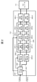
- FIG. 3 is a diagram showing a schematic internal configuration example of the basic LUT correction unit 204 and the linear approximation correction unit 205 in the first mode.
- the basic LUT correction unit 204 has a table for storing correction value data which is the reverse characteristic of distortion corresponding to a 16-bit input X coordinate value in advance, and outputs conversion data corresponding to the input X coordinate value. Correct the distortion. For example, when the data width of the X coordinate value is 16 bits, the memory capacity of the LUT is about 1 Mbit because the number of X coordinates is 65536. In this embodiment, only the basic LUT is prepared without preparing the LUT for distortion correction for each of the X scan and the Y scan for the scan speed, the observation magnification, and the rotation.
- the memory capacity of the basic LUT is, for example, about 1 Mbit when the coordinates are represented by 16 bit digital data, and about 2 Mbit when this is represented by two equations of the X coordinate and the Y coordinate. With this level of capacity, it can be built into an FPGA (Field-Programmable Gate Array), for example, and no external memory is required. Therefore, cost reduction can be realized.
- FPGA Field-Programmable Gate Array
- the total memory capacity is about 8.4 Mbit.
- the straight line approximation correction unit 205 does not correct all the X coordinate values, but approximates the curve with a straight line and approximates each (scan). Corrects distortion (speed, observation magnification, rotation).
- the linear approximation correction unit can be configured by, for example, a multiplier 301, an adder 302, a selector 303, a comparator 304, and a register.
- the register is necessary for setting the slope of the parameter used in the distortion correction, the offset, and the setting value of the change point. Since the parameters set in the register are provided for each change point, the number of parameters set in the register increases or decreases depending on the number of change points.
- the memory capacity can be reduced as compared with the method of correcting all by LUT (conventional example). That is, in the present embodiment, the LUT is provided only in the basic LUT correction unit 204, and the LUT is not provided in other parts (straight line approximation correction unit 205 or curve approximation correction unit 1001 described later). Therefore, the memory capacity can be reduced.
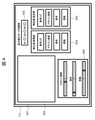
- FIG. 4 is a diagram showing a configuration example of a GUI (Graphical User Interface) according to the present embodiment.
- the GUI 401 displayed on the display of the computer 113 with a display includes, for example, an observation screen 402, a distortion correction mode switching unit 403, a correction value acquisition unit 404, a correction value setting unit 405, and an observation condition setting unit 406.
- the observation screen 402 is a display area for the user to visually confirm the observation sample.
- the observation condition setting unit 406 is an area for the user to set (set to an arbitrary value) a scan speed value, an observation magnification value, and a rotation value (angle value).
- the distortion correction mode switching unit 403 is an area for the user to set a desired distortion correction mode.
- the correction value acquisition unit 404 is an area used when acquiring a correction value.
- the correction value setting unit 405 is a region used when the correction value is set in the basic LUT correction units 204-1 and 204-2, the linear approximation correction unit 205, or the curve approximation correction unit 1001 (described later).
- the user sets the combination of the basic LUT correction and the linear approximation correction in the first mode, the combination of the basic LUT correction and the curve approximation correction (described later) in the second mode, and the rise of the scan waveform on the GUI 401. It is possible to arbitrarily select and switch between the third mode in which the portion and the falling portion are not used for imaging.
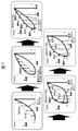
- FIG. 5 is a schematic view showing the state of the rising portion and the falling portion of the scan.
- the third mode in which the rising and falling parts of the scan are not used for imaging, when the screen size is 1280 x 960 in high-speed scanning, 200 ⁇ s is required per X scan.
- the first mode and the second mode it is 125 ⁇ s, which is reduced by about 70 ms per image.
- the third mode instead of performing the calculation by correction, only the central part of the scan waveform having a small distortion dependence and a relatively high linearity is used for imaging. Therefore, the rising and falling portions of the scan waveform are not used for imaging. Therefore, it is possible to selectively suppress the charge-up caused by the sample of the insulating material that occurs at the beginning of the scan.
- the third mode is used.
- the mode can be selectively switched and set.
- FIG. 6 is a flowchart for explaining the distortion correction process by linear approximation of the present embodiment.
- the distortion correction is performed independently in the X direction and the Y direction of the primary electron beam. Further, in the present embodiment, the processing is performed in the order of scan speed correction ⁇ magnification correction ⁇ rotation correction, but the order of these processing is arbitrary, and any correction processing may be executed first.
- Step 601 After starting the processing, the waveform acquisition unit 110 acquires the scan waveform and inputs it to the scan generation unit 201.
- Step 602 The scan generation unit 201 is acquired by the scan waveform acquired in step 601 and the reference waveform for calculating the amount of distortion (ideal waveform: for example, the slowest scan in the scanning electron microscope (charged particle beam device) 100). The waveform is compared with the scan waveform with the least distortion), and the difference between them is measured as the amount of distortion.
- ideal waveform for example, the slowest scan in the scanning electron microscope (charged particle beam device) 100.
- Step 603 The scan generation unit 201 calculates the inverse characteristic of the strain amount measured in step 602.
- Step 604 The scan generation unit 201 sets a correction value, which is an inverse characteristic calculated in step 603, for the LUTs of the basic LUT correction units 204-1 and 204-2.
- the scan generation unit 201 sets an arbitrary number of scan speed patterns, calculates a correction value (parameter) of the reverse characteristic from the strain amount for each setting, and is a straight line with respect to the scan speed correction units 207-1 and 207-2. Set the correction value for approximation correction.
- Step 606 Similar to the scan speed, the scan generation unit 201 sets an arbitrary number of patterns of magnification, calculates the correction value (parameter) of the inverse characteristic from the amount of distortion caused by the magnification, and causes the magnification correction units 208-1 and 208-2. Then, a correction value for linear approximation correction is set.
- Step 607 The scan generation unit 201 sets an arbitrary number of rotation (rotation angles) patterns, calculates correction values (parameters) for the amount of distortion of each pattern, and linearly approximates the rotation correction units 209-1 and 209-2. Set to the correction value for correction.
- the scan waveform output from the scan generation unit 201 is the basic LUT correction units 204-1 and 204-2, the scan speed correction units 207-1 and 207-2, the magnification correction units 208-1 and 208-2, and the rotation.
- the elements are corrected (distortion correction and delay time adjustment) by the correction units 209-1 and 209-2 and the time correction units 206-1 and 206-2, respectively, and output to the D / A converter 111.
- the D / A converter 111 converts the digital waveform into an analog waveform and outputs it to the deflector 104.
- Step 609 The deflector scans the primary electron beam with a highly linear scan waveform to display a distortion-free image.
- FIG. 7 is a diagram showing a specific example of correction processing of the X-direction scan waveform signal by linear approximation.
- the scan generation unit 201 acquires the amount of distortion, which is the difference between the reference waveform (ideal waveform of a straight line) and the distorted measurement waveform, and sets the reverse characteristic of the amount of distortion in the basic LUT correction unit 204-1. Then, the basic LUT correction unit 204-1 distorts the scan waveform signal in the opposite direction. As a result, the delay-dependent distortion amount of the responsiveness of the deflection coil 1401 is canceled by the distortion amount in the reverse direction due to the basic LUT, and is corrected to a scan waveform with high linearity.
- the number of change points of the linear approximation is 4 for each of the scan speed correction, the magnification correction, and the rotation correction. Therefore, for each of the change point a, the change point b, the change point c, the change point d, the slope 1 connecting each change point and the end point, the slope 2, the slope 3, the slope 4, and the slope 5. Offset 1, offset 2, offset 3, offset 4, and offset 5 corresponding to each inclination are stored in the acquisition waveform storage memory 115 in the waveform acquisition unit 110 as correction value parameters.
- FIG. 8 is a diagram showing an example of a calculation method and a calculation formula for the inclination value.
- the method for calculating the slope 2 is a value obtained by dividing the X coordinate value of the change point b and the value obtained by subtracting the offset 2 by the time value of the change point b.
- slope ⁇ 5 types horizontal axis value of the change point ⁇ 4 types; offset value ⁇ offset value
- the register setting accesses each correction unit from the computer, the number of accesses increases and the time required for correction increases as the number of parameters for register setting increases.
- the scan scan is delayed and the scan waveform is distorted.
- the amount of distortion at each scan speed is measured in advance, and the correction value, which is the opposite characteristic, is stored in the acquisition waveform storage memory 115 in the waveform acquisition unit 110. Then, the amount of distortion due to the influence of the scan speed is canceled by the linear approximation waveform drawn from the stored correction value parameters a and b, the slope 1 corresponding to each point and the end point, and the slope 2 and the slope 3. It becomes possible. By canceling the amount of strain, an ideal waveform with high linearity can be generated.
- the observation magnification condition is low, that is, when the scan scan is performed over a wide range, the range in which the beam is scanned to the end in the X direction and the beam is returned to the opposite end of the beam scan start is long, so the scan that scans the beam is performed.
- the waveform is distorted with a delay. In this case, the distortion of the waveform due to the magnification is measured, and the correction value which is the opposite characteristic is stored in the acquisition waveform storage memory 115 in the waveform acquisition unit 110.
- the distortion amount due to the influence of the magnification is canceled by the linear approximation waveform drawn from the change points a and b, which are the stored correction value parameters, and the slope 1, the slope 2, and the slope 3 corresponding to each point and the end point. Can be done. By canceling the amount of strain, an ideal waveform with high linearity can be generated.
- the scan waveform may be distorted.
- the amount of strain at each rotation angle is measured, and the correction value, which is the reverse characteristic of the measured amount of strain, is stored in the acquired waveform storage memory 115 in the waveform acquisition unit 110.
- a linear approximation waveform is drawn from the stored correction value parameters a and b, and the slope 1, the slope 2, and the slope 3 connecting each point and the end point. Then, by calculating the drawn linear approximation waveform and the distorted waveform, the distortion due to rotation can be canceled.
- the time correction unit 206 can adjust the time for correction by setting the register.
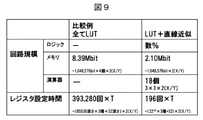
- FIG. 9 is a diagram showing a comparison of circuit scales between a method of correcting all by LUT (comparative example) and a method of correcting by basic LUT and linear approximation (this embodiment). According to this embodiment, it can be seen that the memory capacity can be reduced to about 25% of the comparative example. Further, it can be seen that the register setting time (the time for transmitting the parameter from the storage unit to the arithmetic unit inside the FPGA) is only 0.05% of the comparative example.
- the distortion amount of the deflection coil is corrected by the basic LUT correction unit, and the distortion depending on each observation condition is corrected in real time by the linear approximation correction.
- FIG. 10 is a diagram showing an example of the internal configuration of the scan waveform generation device 112 in the second mode.
- the scan waveform generation device 112 receives commands from the computer 113 (scan setting commands for instructing scan parameters and correction commands for acquiring distortion correction values) and outputs from the waveform acquisition unit 110 as inputs, and the scan generation unit 112.
- 201 a basic LUT correction unit 204-1 that corrects the X-direction scan signal 202, a basic LUT correction unit 204-2 that corrects the Y-direction scan signal 203, a curve approximation correction unit 1001, and a time correction unit 206.
- the curve approximation correction unit 1001 corrects the scan speed correction unit 1002-1 for correcting the scan speed distortion in the X direction, the scan speed correction unit 1002-2 for correcting the scan speed distortion in the Y direction, and the magnification distortion in the X direction.
- the basic LUT correction units 204-1 and 204-2 have and input a table for storing correction value data which is an inverse characteristic of distortion corresponding to a 16-bit input X coordinate value in advance.
- the conversion data corresponding to the X coordinate value is output to correct the distortion.
- the curve approximation correction unit 1001 uses a small-capacity LUT to approximate the vicinity of the conversion point (where the slope changes significantly) of the approximate straight line in the first mode with a smooth curve, respectively (scan speed, observation magnification, rotation). Correct the distortion of. In the straight line approximation correction, the slope near the change point becomes steep and the correction accuracy becomes coarse, but in the curve approximation correction, the correction accuracy is higher than the straight line approximation correction because the curve can be smoothly corrected by the small capacity LUT. In addition, by limiting the range of curve correction, the memory capacity and correction time can be reduced as compared with the above-mentioned comparative example.
- the small-capacity LUT is prepared for each of the scan speed correction unit, the magnification correction unit, and the rotation correction unit for the X scan and the Y scan.
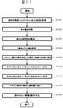
- FIG. 11 is a flowchart for explaining the distortion correction process by curve approximation of the present embodiment (second mode).
- the slope near the change point changes greatly, so that the correction may be coarse.
- the correction by curve approximation by setting the correction value to a small capacity LUT (separate from the basic LUT), the vicinity of the change point becomes smooth. Therefore, it is possible to increase the accuracy of correction as compared with the first mode.
- Step 1101 The scan generation unit 201 acquires the scan waveform acquired by the waveform acquisition unit 110.
- Step 1102 The scan generation unit 201 compares the scan waveform acquired in step 1101 with the reference waveform for strain measurement (ideal waveform: for example, the waveform acquired by the slowest scan), and uses the difference as the strain amount. measure.
- the reference waveform for strain measurement ideal waveform: for example, the waveform acquired by the slowest scan
- Step 1103 The scan generation unit 201 calculates the inverse characteristic of the strain amount measured in step 1102.
- Step 1104 The scan generation unit 201 sets correction values having opposite characteristics in the basic LUT correction units 204-1 and 204-2.
- the scan generation unit 201 sets an arbitrary number of scan speed patterns, and calculates an inverse characteristic correction value (parameter) from the amount of distortion obtained near each change point (start point and end point are specified) of each pattern. , The correction value is set to the small capacity LUT (not shown) of the scan speed correction units 1002-1 and 1002-2.
- Step 1106 the scan generation unit 201 sets an arbitrary number of magnification patterns, calculates the correction value (parameter) of the inverse characteristic from the strain amount near each change point of each pattern (the start point and the end point are specified), and calculates the correction value (parameter). Correction values are set in the small-capacity LUTs (not shown) of the magnification correction units 1003-1 and 1003-2.
- Step 1107 the scan generation unit 201 sets an arbitrary number of rotation (angle) patterns, and corrects the inverse characteristic from the distortion amount near each change point (start point and end point are specified) of each pattern (parameter). Is calculated, and a correction value is set in the small capacity LUT (not shown) of the rotation correction units 1004-1 and 1004-2.
- the scan waveform output from the scan generation unit 201 is the basic LUT correction units 204-1 and 204-2, the scan speed correction units 1002-1 and 1002-2, the magnification correction units 1003-1 and 1003-2, and the rotation. It is corrected by the correction units 1004-1 and 1004-2 and output to the D / A converter 111.
- the D / A converter 111 converts the corrected digital waveform into an analog waveform, and sends the converted scan waveform (analog waveform) to the deflector 104.
- Step 1109 The deflector 104 displays a distortion-free image by scanning the primary electron beam. The correction is performed independently for the X direction and the Y direction of the primary electron beam.
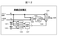
- FIG. 12 is a diagram showing a configuration example of an arithmetic circuit for curve approximation correction (second mode).
- the calculation circuit for curve approximation correction can be configured by, for example, an adder 1203, a comparator 1204, a selector 1205, a data type conversion unit 1206, and a range selection unit 1207.
- the scan generation unit 201 determines from the calculation result of the small capacity LUT the start point 1201 and the end point 1202 (start point and end point of the point to be approximated by the curve (near the change point)): to which range the small capacity LUT is applied to approximate the curve.
- the information shown) is calculated and the register is set.
- the comparator 1204 compares the scan coordinates with the calculated start point 1201 and end point 1202.
- the range selection unit 1207 selects a range, and the selector 1205 corrects or controls the scan waveform. For example, the correction is performed by adding the scan coordinates 16 bits and the small capacity LUT data 9 bits, and the data type is converted into integer data and then output.
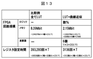
- FIG. 13 is a diagram showing the results of comparing the circuit scales of the method of correcting all by LUT (comparative example) and the method of basic LUT correction + curve approximation correction (second mode).
- the second mode is a calculation based on a LUT (small capacity LUT), so only one arithmetic unit is used for each correction unit. Therefore, the number of arithmetic units used is reduced as compared with the first mode. Further, it can be seen that the register setting time (the time for transmitting the parameter from the storage unit to the arithmetic unit inside the FPGA) is about 1% of the comparative example, and the distortion correction can be performed in real time.
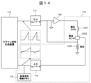
- FIG. 14 is a diagram showing an example of the internal configuration of the waveform acquisition unit 110 according to the present embodiment.
- the waveform acquisition unit 110 includes an A / D converter 114, an acquisition waveform storage memory 115, a deflection coil 1401, a current sensor 1402, and a resistor 1403.
- the waveform acquisition unit 110 acquires the amount of distortion by measuring the current of the deflection coil 1401 with the current sensor 1402 and then comparing it with a reference waveform (ideal waveform: the waveform acquired by the slowest scan). Then, this strain amount is recorded in the acquired waveform storage memory 115, and is output as a scan waveform to the scan waveform generator 112.
- the current range can be adjusted by the resistor 1403, and a desired level of current waveform can be acquired.
- This makes it possible to acquire not only the distortion due to the delay in the response of the deflection coil 1401 but also the scan distortion due to each observation condition by using the apparatus. That is, it is possible to correct the distortion due to a slight difference in the device and the scan distortion due to the aged deterioration of the device as many times as necessary.
- FIG. 15 is a diagram showing an outline of an image connecting function according to the present embodiment.
- the image joining function is a function of capturing a plurality of images and joining them by software processing to generate one image.
- the image before joining is captured, the image without distortion is acquired by extending the scan time (the image of the rising portion and the falling portion is not used for image generation). ), As a result, the throughput of the image connection function was significantly reduced.
- the scan is magnified and the beam is irradiated, the sample damage is worsened.
- the scanning time is reduced and the throughput is improved accordingly. Further, since it is not necessary to irradiate the joint portion where the scan has been enlarged with a beam, it is possible to improve the accuracy of the image joint and reduce the damage to the sample.
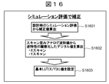
- FIG. 16 is a flowchart for explaining the correction value calculation process by simulation evaluation.
- Step 1601 The computer 113 performs a simulation evaluation from the design value of the charged particle beam device, and calculates a correction value which is an inverse characteristic of the scan output waveform from the simulation result.
- Step 1602 The computer 113 calculates the discretized digital value of the inverse characteristic from the scan distortion analog waveform. The calculation of the discretized digital values of the inverse characteristics is performed for each of the X-direction scan and the Y-direction scan.
- Step 1603 The computer 113 sets the correction values calculated in step 1602 in the basic LUT correction units 204-1 and 204-2.
- the amount of distortion of the deflection coil 1401 can be evaluated at the design stage.
- FIG. 17 is a flowchart for explaining the correction value calculation process by the waveform acquisition unit 110.
- the correction value calculation process by the waveform acquisition unit 110 can be executed at a stage where only the FPGA circuit exists (a stage where the actual machine of the charged particle beam device does not yet exist).
- Step 1701 The waveform acquisition unit 110 measures the scan output waveform.
- Step 1702 The waveform acquisition unit 110 calculates a digital value of the inverse characteristic from the scan waveform measured in step 1701. When calculating the digital value of the inverse characteristic, the waveform acquisition unit 110 calculates each of the X-direction scan and the Y-direction scan. Further, the waveform acquisition unit 110 calculates correction values for each of the scan speed, the observation magnification, and the rotation.
- Step 1703 The waveform acquisition unit 110 sets values in the basic LUT correction units 204-1 and 204-2.
- Step 1704 The waveform acquisition unit 110 sets a correction value in the linear approximation correction unit 205 or the curve approximation correction unit 1001 for each of the X-direction scan and the Y-direction scan.
- the correction value calculation process by the waveform acquisition unit 110 is not a process of calculating the correction value using the actual machine of the charged particle beam device. Therefore, it is not possible to measure the amount of strain due to the difference between the devices. However, the strain caused by the deflection coil 1401 and each observation condition can be measured, and various strains can be corrected.
- FIG. 18 is a flowchart for explaining the correction value calculation process at the time of shipment of the device. That is, this correction value calculation process is related to the acquisition of the correction value using the actual machine.
- Step 1801 The scan generation unit 201 measures the scan output waveform from the device at the time of shipment.
- Step 1802 The scan generation unit 201 calculates a discretized digital value of the inverse characteristic from the analog value of the scan distortion waveform.
- Step 1803 The scan generation unit 201 sets the digital values calculated in step 1802 in the basic LUT correction units 204-1 and 204-2.
- Step 1804 The scan generation unit 201 calculates the inverse characteristics of the distortion due to the scan speed, the observation magnification, and the rotation for each of the X-direction scan and the Y-direction scan, and sets them in the linear approximation correction unit 205 or the curve approximation correction unit 1001.
- FIG. 19 is a flowchart for explaining the correction value calculation process at the time of user use.
- Step 1901 The scan generation unit 201 measures the scan output waveform from the post-shipment device (device in use: for example, a charged particle beam device that has been used for many years).
- Step 1902 The scan generation unit 201 calculates a digital value of the inverse characteristic from the scan waveform measured in step 1901. When calculating the digital value of the inverse characteristic, it is calculated for each X-direction scan and Y-direction scan. Further, the scan generation unit 201 calculates the scan speed, the observation magnification, and the correction value by rotation for each of the X-direction scan and the Y-direction scan.
- Step 1903 The scan generation unit 201 sets a correction value in the basic LUT correction unit 204.
- Step 1904 The scan generation unit 201 sets a correction value in the straight line approximation correction unit 205 or the curve approximation correction unit 1001.
- Step 1905 The scan generation unit 201 measures the scan waveform again in response to the user's instruction.
- Step 1906 The scan generation unit 201 acquires a correction value from the waveform measured in step 1905, and resets the correction value in the basic LUT correction units 204-1 and 204-2. Similarly, the scan generation unit 201 resets the correction value to the linear approximation correction unit 205 or the curve approximation correction unit 1001 for each scan speed, observation magnification, and rotation. That is, after shipment, the user can arbitrarily re-correct the scan distortion due to the aged deterioration of the device. Therefore, the maintenance of the device can be performed by the user himself / herself.
- the charged particle beam apparatus 100 may be provided with functions corresponding to the above-mentioned first mode, second mode, and third mode, and one of them may be selected so that the sample 08 can be scanned and observed. , The function corresponding to the first mode or the second mode and the third mode may be provided so that the sample 108 can be observed. Further, the charged particle beam apparatus 100 may be configured to have either the function of the first mode or the second mode.
- the distortion characteristic of the deflection coil is corrected by using the basic LUT that stores the parameter for correcting the scan waveform (digital scan waveform).
- the linear approximation correction unit 205 and the curve approximation correction unit 1001 change the correction parameters acquired from the basic LUT according to the conditions including at least one of the scan speed, the magnification, and the rotation.
- the correction parameters are (i) the first parameter set of the inverse characteristics of the distortion characteristics under predetermined conditions (parameters for correcting the distortion due to the delay in the response of the deflection coil) stored in the basic LUT.
- (ii) It is composed of a combination of a second parameter set (parameters generated by changing the correction parameters of the basic LUT according to each condition) according to each condition of scan speed, magnification, and rotation.
- the second parameter set is a parameter for distortion correction by linear approximation or a parameter for distortion correction by curve approximation that corrects distortion corresponding to a condition including at least one of scan speed, magnification, and rotation. ..
- the distortion characteristic is corrected by executing the second correction (correction according to each condition) by the second parameter set.
- magnification distortion, distortion of the current flowing through the deflection coil of the electron beam, scanning speed, and distortion due to the scanning direction (raster rotation) of the electron probe can be corrected for all conditions, linear approximation or curve.
- scan distortion correction can improve the throughput and connection accuracy of the image connection function. Further, since the scan waveform acquisition means can correct the scan distortion even after the device is shipped, the distortion due to aged deterioration can be re-corrected.
- the function of this embodiment can also be realized by a software program code.
- a storage medium in which the program code is recorded is provided to the system or the device, and the computer (or CPU or MPU) of the system or the device reads out the program code stored in the storage medium.
- the program code itself read from the storage medium realizes the function of the above-described embodiment, and the program code itself and the storage medium storing the program code itself constitute the present disclosure.
- Examples of the storage medium for supplying such a program code include a flexible disk, a CD-ROM, a DVD-ROM, a hard disk, an optical disk, a magneto-optical disk, a CD-R, a magnetic tape, a non-volatile memory card, and a ROM. Etc. are used.
- the OS operating system
- the processing enables the function of the above-described embodiment to be realized. You may. Further, after the program code read from the storage medium is written in the memory on the computer, the CPU of the computer or the like performs a part or all of the actual processing based on the instruction of the program code, and the processing is performed. May realize the function of the above-described embodiment.
- the program code is distributed as a storage means such as a hard disk or a memory of the system or an apparatus, or a storage medium such as a CD-RW or a CD-R.
- the computer (or CPU or MPU) of the system or device may read and execute the program code stored in the storage means or the storage medium at the time of use.
- control lines and information lines are shown as necessary for explanation, and the product does not necessarily show all the control lines and information lines. All configurations may be interconnected.
- Scan waveform generator 113 computer with display, 114 A / D converter, 115 acquisition waveform storage memory, 201 scan generator, 202 X-direction scan signal, 203 Y-direction scan signal, 204 basic LUT correction unit, 205 linear approximation correction unit , 206 time correction unit, 207 scan speed correction unit, 208 magnification correction unit, 209 rotation correction unit, 301 multiplier, 302 adder, 303 selector, 304 comparer, 401 GUI, 402 observation screen, 403 distortion correction mode switching unit , 404 correction value acquisition unit, 405 correction value setting unit, 406 observation condition setting unit, 1001 curve approximation correction unit, 1201 start point, 1202 end point, 1203 adder, 1204 comparer, 1205 selector, 1206 data type conversion unit, 1207 range Selector, 1401 deflection coil, 1402 current sensor, 1403 resistor
Landscapes
- Chemical & Material Sciences (AREA)
- Analytical Chemistry (AREA)
- Electron Sources, Ion Sources (AREA)
Abstract
Description
図1は、実施形態による走査型電子顕微鏡の構成例を示す図である。図1に示すように、走査型電子顕微鏡100は、電子源101と、第1コンデンサレンズ102と、第2コンデンサレンズ103と、偏向器104と、筐体105と、対物レンズ106と、試料室107と、試料108と、アンプ109と、波形取得部110と、D/Aコンバータ111と、スキャン波形生成装置112と、ディスプレイ付きコンピュータ113(以下、単に「コンピュータ」と称する場合もある)と、を備える。
図2は、第1モード(後述の直線近似)によるスキャン波形生成装置112の内構成例を示す図である。スキャン波形生成装置112は、コンピュータ113からのコマンド(スキャンパラメータを指示するためのスキャン設定コマンドや歪補正値を取得するための補正コマンド)および波形取得部110からの出力を入力とし、スキャン生成部201と、X方向スキャン信号202を補正する基本LUT補正部204-1と、Y方向スキャン信号203を補正する基本LUT補正部204-2と、直線近似補正部205と、時間補正部206と、を備える。直線近似補正部205は、X方向のスキャン速度歪みを補正するスキャン速度補正部207-1と、Y方向のスキャン速度歪みを補正するスキャン速度補正部207-2と、X方向の倍率歪みを補正する倍率補正部208-1と、Y方向の倍率歪みを補正する倍率補正部208-2と、X方向の回転(ラスターローテーション)歪みを補正する回転補正部209-1と、Y方向の回転(ラスターローテーション)歪みを補正する回転補正部209-2と、を有する。
図3は、第1モードによる基本LUT補正部204および直線近似補正部205の概略内部構成例を示す図である。
図4は、本実施形態によるGUI(Graphical User Interface)の構成例を示す図である。ディスプレイ付きコンピュータ113のディスプレイ上に表示されるGUI401は、例えば、観察画面402と、歪み補正モード切替部403と、補正値取得部404と、補正値設定部405と、観察条件設定部406と、を備える。観察画面402は、ユーザが観察試料の目視確認するための表示領域である。観察条件設定部406は、ユーザがスキャン速度値と、観察倍率値と、回転値(角度値)とを設定(任意の値に設定)するための領域である。歪み補正モード切替部403は、ユーザが所望の歪み補正モードに設定するための領域である。
図5は、スキャン立ち上がり部分と立ち下がり部分の様子を示す概略図である。第1モードおよび第2モードが選択された場合、スキャン波形は、理想的な直線性の高い波形に補正されるため、比較的歪みやすい立ち上がり部分および立ち下り部分を撮像に用いることが可能となる。そのため第3モードよりも観察スループットが向上する。
図6は、本実施形態の直線近似による歪み補正処理を説明するためのフローチャートである。なお、歪み補正は、一次電子ビームのX方向とY方向に対して独立して行われる。また、本実施形態では、スキャン速度補正→倍率補正→回転補正の順で処理しているが、これらの処理の順番は任意であり、どの補正処理を先に実行してもよい。
処理開始後、波形取得部110は、スキャン波形を取得し、スキャン生成部201に入力する。
スキャン生成部201は、ステップ601で取得したスキャン波形と、歪み量算出のための基準波形(理想的な波形:例えば、走査型電子顕微鏡(荷電粒子線装置)100において最も速度が遅いスキャンによって取得した波形であって、最も歪みが少ないスキャン波形)と比較し、それらの差異を歪み量として計測する。
スキャン生成部201は、ステップ602で計測した歪み量の逆特性を算出する。
スキャン生成部201は、基本LUT補正部204-1および204-2のLUTに対して、ステップ603で算出した逆特性である補正値を設定する。
スキャン生成部201は、スキャン速度を任意に数パターン設定し、設定毎の歪み量から逆特性の補正値(パラメータ)を算出し、スキャン速度補正部207-1および207-2に対して、直線近似補正のための補正値を設定する。
スキャン生成部201は、スキャン速度と同様に、倍率を任意に数パターン設定し、それによる歪み量から逆特性の補正値(パラメータ)を算出し、倍率補正部208-1および208-2に対して、直線近似補正のための補正値を設定する。
スキャン生成部201は、回転(回転角度)を任意の数パターン設定し、各パターンの歪み量に対する補正値(パラメータ)を算出し、回転補正部209-1および209-2に対して、直線近似補正のための補正値に設定する。
その後、スキャン生成部201から出力されたスキャン波形は、基本LUT補正部204-1および204-2、スキャン速度補正部207-1および207-2、倍率補正部208-1および208-2、回転補正部209-1および209-2、時間補正部206-1および206-2においてそれぞれ要素について補正(歪み補正および遅延時間調整)され、D/Aコンバータ111へ出力される。そして、D/Aコンバータ111は、デジタル波形をアナログ波形に変換し、偏向器104に出力する。
偏向器は、直線性の高いスキャン波形で一次電子ビームを走査することで歪みのない画像を表示する。
上記フローチャートで示した直線近似による歪み補正処理の具体例について説明する。図7は、直線近似によるX方向スキャン波形信号の補正処理の具体例を示す図である。
図8は、傾き値の算出方法と算出式の例を示す図である。傾き2の算出方法は、変化点bのX座標値とオフセット2を減算した値を変化点bの時間値で除算した値となる。スキャン速度のXスキャンの歪みに対する直線近似補正を行う場合、変化点4点でレジスタ設定するパラメータは、合計で14種(傾き→5種;変化点の横軸の値→4種;オフセット値→5種)となる。レジスタ設定は、コンピュータから各補正部にアクセスするため、レジスタ設定するパラメータが多くなると、アクセス回数が増え、補正に要する時間も多くなる。
図9は、全てLUTで補正する手法(比較例)と基本LUTおよび直線近似にて補正する手法(本実施形態)の回路規模の比較を示す図である。本実施形態によれば、メモリ容量が比較例の約25%まで低減できることが分かる。また、レジスタ設定時間(FPGA内部において、パラメータをその格納部から演算部まで伝送する時間)は、比較例の僅か0.05%であることが分かる。つまり、直線近似にすることで、倍率歪み、電子ビームの偏向コイルに流れる電流の歪み、スキャン速度、電子プローブの走査方向(ラスターローテーション)による歪みに対して、すべての条件毎に補正を行うことができ、回路規模を低減し、低価格な装置を実現する。また、レジスタ設計時間も短縮でき、高速スキャン時にも対応が可能となる。
本実施形態は、偏向コイルの歪み量は、基本LUT補正部で補正し、各観察条件依存の歪みは、直線近似補正でリアルタイムに補正を行う。
図10は、第2モードによるスキャン波形生成装置112の内構成例を示す図である。スキャン波形生成装置112は、コンピュータ113からのコマンド(スキャンパラメータを指示するためのスキャン設定コマンドや歪補正値を取得するための補正コマンド)および波形取得部110からの出力を入力とし、スキャン生成部201と、X方向スキャン信号202を補正する基本LUT補正部204-1と、Y方向スキャン信号203を補正する基本LUT補正部204-2と、曲線近似補正部1001と、時間補正部206と、を備える。曲線近似補正部1001は、X方向のスキャン速度歪みを補正するスキャン速度補正部1002-1と、Y方向のスキャン速度歪みを補正するスキャン速度補正部1002-2と、X方向の倍率歪みを補正する倍率補正部1003-1と、Y方向の倍率歪みを補正する倍率補正部1003-2と、X方向の回転歪みを補正する回転補正部1004-1と、Y方向の回転歪みを補正する回転補正部1004-2と、を有する。
図11は、本実施形態(第2モード)の曲線近似による歪み補正処理を説明するためのフローチャートである。第1モードの直線近似補正は、変化点付近の傾きが大きく変化するため、補正が粗くなる場合がある。一方、曲線近似による補正は、補正値を小容量LUT(基本LUTとは別に)に設定することで、変化点付近が滑らか形となる。そのため第1モードよりも補正の精度を高くすることが可能となる。
スキャン生成部201は、波形取得部110により取得したスキャン波形を取得する。
スキャン生成部201は、ステップ1101で取得したスキャン波形と、歪み計測のための基準波形(理想的な波形:例えば、速度が最も遅いスキャンによって取得した波形)とを比較し、差異を歪み量として計測する。
スキャン生成部201は、ステップ1102で計測した歪み量の逆特性を算出する。
スキャン生成部201は、基本LUT補正部204-1および204-2に逆特性である補正値を設定する。
スキャン生成部201は、スキャン速度を任意に数パターン設定し、各パターンの各変化点付近(始点と終点が指定される)における得られた歪み量から逆特性の補正値(パラメータ)を算出し、その補正値をスキャン速度補正部1002-1および1002-2の小容量LUT(図示せず)に設定する。
スキャン生成部201は、同様に、倍率を任意に数パターン設定し、各パターンの各変化点付近(始点と終点が指定される)における歪み量から逆特性の補正値(パラメータ)を算出し、倍率補正部1003-1および1003-2の小容量LUT(図示せず)に補正値を設定する。
スキャン生成部201は、同様に、回転(角度)を任意の数パターンを設定し、各パターンの各変化点付近(始点と終点が指定される)の歪み量から逆特性の補正値(パラメータ)を算出し、回転補正部1004-1および1004-2の小容量LUT(図示せず)に補正値を設定する。
その後、スキャン生成部201から出力されたスキャン波形が、基本LUT補正部204-1および204-2、スキャン速度補正部1002-1および1002-2、倍率補正部1003-1および1003-2、回転補正部1004-1および1004-2において補正され、D/Aコンバータ111へ出力される。D/Aコンバータ111は、補正されたデジタル波形をアナログ波形に変換し、変換されたスキャン波形(アナログ波形)を偏向器104に送る。
偏向器104は、一次電子ビームを走査することで歪みのない画像を表示する。なお、補正は、一次電子ビームのX方向とY方向に対して独立して行われる。
図12は、曲線近似補正(第2モード)の演算回路の構成例を示す図である。曲線近似補正の演算回路は、例えば、加算器1203と、比較器1204と、セレクタ1205と、データ型変換部1206と、範囲選択部1207と、によって構成することができる。
図13は、全てLUTで補正する手法(比較例)と基本LUT補正+曲線近似補正する手法(第2モード)の回路規模の比較結果を示す図である。
図14は、本実施形態による波形取得部110の内部構成例を示す図である。波形取得部110は、A/Dコンバータ114と、取得波形格納メモリ115と、偏向コイル1401と、電流センサ1402と、抵抗1403を備えている。波形取得部110は、偏向コイル1401の電流を電流センサ1402で測定した後、基準となる波形(理想的な波形:最も速度が遅いスキャンによって取得した波形)との比較で歪み量を取得する。そして、この歪み量は、取得波形格納メモリ115に記録され、スキャン波形生成装置112にスキャン波形として出力される。
図15は、本実施形態による画像つなぎ機能の概略を示す図である。画像つなぎ機能は、画像を複数枚撮像し、それをソフト処理によりつなぎ合せて一枚の画像を生成する機能である。従来(第3モード)では、つなぎ合わせる前の画像を撮像する際に、スキャン時間を拡大することで歪みのない画像を取得しており(立ち上がり部分と立下り部分の画像を画像生成に用いない)、これにより画像つなぎ機能のスループットが大幅に低下していた。加えてスキャンを拡大してビーム照射しているため、試料ダメージも悪化する。
図16は、シミュレーション評価による補正値算出処理を説明するためのフローチャートである。
コンピュータ113は、荷電粒子線装置の設計値からシミュレーション評価を行い、シミュレーション結果からスキャン出力波形の逆特性である補正値を算出する。
コンピュータ113は、スキャン歪みアナログ波形から逆特性の離散化したデジタル値を算出する。逆特性の離散化したデジタル値の算出は、X方向スキャンおよびY方向スキャンそれぞれに対して実行される。
コンピュータ113は、ステップ1602で算出した補正値を基本LUT補正部204-1および204-2に設定する。
図17は、波形取得部110による補正値算出処理を説明するためのフローチャートである。波形取得部110による補正値算出処理は、FPGA回路のみ存在する段階(荷電粒子線装置の実機がまだ存在しない段階)で実行することができる。
波形取得部110は、スキャン出力波形を計測する。
波形取得部110は、ステップ1701で計測したスキャン波形から逆特性のデジタル値を算出する。逆特性のデジタル値を算出する際は、波形取得部110は、X方向スキャンおよびY方向スキャンごとに算出する。また、波形取得部110は、スキャン速度、観察倍率、および回転のそれぞれについて補正値を算出する。
波形取得部110は、基本LUT補正部204-1および204-2に値を設定する。
波形取得部110は、X方向スキャンおよびY方向スキャンごとに、直線近似補正部205もしくは曲線近似補正部1001に補正値を設定する。
図18は、装置出荷時の補正値算出処理を説明するためのフローチャートである。つまり、この補正値算出処理は、実機を用いた補正値の取得に関するものである。
スキャン生成部201は、出荷時の装置からスキャン出力波形を計測する。
スキャン生成部201は、スキャン歪み波形のアナログ値から逆特性の離散化したデジタル値を算出する。
スキャン生成部201は、ステップ1802で算出したデジタル値を基本LUT補正部204-1および204-2に設定する。
スキャン生成部201は、X方向スキャンおよびY方向スキャンごとに、スキャン速度、観察倍率、および回転による歪みの逆特性を算出し、直線近似補正部205もしくは曲線近似補正部1001に設定する。
図19は、ユーザ使用時の補正値算出処理を説明するためのフローチャートである。
スキャン生成部201は、出荷後の装置(使用中の装置:例えば、何年も使用している荷電粒子線装置)からスキャン出力波形を計測する。
スキャン生成部201は、ステップ1901で計測したスキャン波形から逆特性のデジタル値を算出する。逆特性のデジタル値を算出する際は、X方向スキャンおよびY方向スキャンごとに算出される。また、スキャン生成部201は、X方向スキャンおよびY方向スキャンごとに、スキャン速度、観察倍率、および回転による補正値を算出する。
スキャン生成部201は、基本LUT補正部204に補正値を設定する。
スキャン生成部201は、直線近似補正部205もしくは曲線近似補正部1001に補正値を設定する。
スキャン生成部201は、ユーザの指示に応答して、再度スキャン波形を計測する。
スキャン生成部201は、ステップ1905で計測した波形から補正値を取得し、基本LUT補正部204-1および204-2に補正値を再設定する。同様に、スキャン生成部201は、スキャン速度、観察倍率、および回転ごとに直線近似補正部205もしくは曲線近似補正部1001に補正値を再設定する。つまり、出荷後、装置の経年劣化によるスキャン歪みをユーザが任意に、再補正を行うことが可能となる。したがって、装置のメンテナンスをユーザ自身で行うことができる。
荷電粒子線装置100において、上述の第1モード、第2モード、及び第3モードに対応するそれぞれの機能を設け、何れかを選択して試料08を走査し、観察できるようにしてもよいし、第1モードあるいは第2モードと第3モードに対応する機能を設け、試料108を観察できるようにしてもよい。また、第1モードあるいは第2モードの何れかの機能を有するように荷電粒子線装置100を構成してもよい。
(i)本実施形態によれば、スキャン波形(デジタルスキャン波形)を補正するためのパラメータを格納する基本LUTを用いて偏向コイルの歪み特性を補正する。また、本実施形態では、直線近似補正部205および曲線近似補正部1001は、スキャン速度、倍率、および回転の少なくとも一つを含む条件に応じて、基本LUTから取得した補正パラメータを変更する。具体的には、補正パラメータは、(i)基本LUTに格納された、所定条件での歪み特性の逆特性の第1パラメータセット(偏向コイルの応答性の遅れによる歪みを補正するパラメータ)と、(ii)スキャン速度、倍率、および回転の各条件に応じた第2パラメータセット(基本LUTの補正パラメータを各条件に応じて変更して生成されたパラメータ)と、の組み合わせで構成される。第2パラメータセットは、スキャン速度、倍率、および回転の少なくとも一つを含む条件に対応する歪みを補正する、直線近似による歪み補正のためのパラメータ、あるいは曲線近似による歪み補正のためのパラメータである。そして、第1パラメータセットによって第1補正を実行した後、第2パラメータセットによって第2補正(各条件に合せた補正)を実行することにより、歪み特性を補正する。このようにすることにより、様々な観察条件で歪みのない画像を逐次観察できる。また、基本LUTによる基本的な像質の改善だけでなく、視野内の測長再現性、画像解析の精度や画像つなぎ機能を改善する件となる。さらに、倍率歪み、電子ビームの偏向コイルに流れる電流の歪み、スキャン速度、電子プローブの走査方向(ラスターローテーション)による歪みに対して、すべての条件毎に補正を行うことができ、直線近似または曲線近似により、回路規模を低減し、低価格な装置を実現することができる。また、スキャン歪み補正により、画像つなぎ機能のスループットおよびつなぎ精度を向上させることができる。さらに、スキャン波形取得手段によって、装置出荷後においてもスキャン歪み補正ができるため、経年劣化による歪みを再補正できる。
Claims (12)
- 試料に荷電粒子線を照射して画像を取得する荷電粒子線装置であって、
前記荷電粒子線を前記試料上で走査させる偏向コイルと、
デジタルスキャン波形をアナログスキャン波形に変換し、当該アナログスキャン波形を前記偏向コイルに出力して駆動させるD/Aコンバータと、
前記デジタルスキャン波形を生成して、前記D/Aコンバータに出力するスキャン波形生成部と、を備え、
前記スキャン波形生成部は、前記デジタルスキャン波形を補正するためのパラメータを格納する基本LUTを有し、前記偏向コイルの歪み特性を補正する補正回路を含む、荷電粒子線装置。 - 請求項1において、
前記スキャン波形生成部は、外部から入力されるモード信号であって、前記歪み特性の補正を実行するか、あるいは前記歪み特性の補正を実行せずにスキャン波形の立ち上がり部と立ち下がり部を用いずに撮像するかを示すモード信号に応じて、前記デジタルスキャン波形を出力する、荷電粒子線装置。 - 請求項2において、
前記モード信号は、直線近似によって前記歪み特性の補正の実行を指示する第1モード信号と、曲線近似によって前記歪み特性の補正の実行を指示する第2モード信号と、前記歪み特性の補正を実行せずにスキャン波形の立ち上がり部と立ち下がり部を用いずに撮像することを指示する第3モード信号とを含み、
前記スキャン波形生成部は、前記第1モード信号あるいは前記第2モード信号を受信した場合には、前記補正回路を前記第1モード信号あるいは前記第2モード信号に対応する歪み補正を実行するように前記補正回路を動作させて補正された前記デジタルスキャン波形を出力し、前記第3モード信号を受信した場合には、前記補正回路を動作させずに前記デジタルスキャン波形を出力する、荷電粒子線装置。 - 請求項3において、
前記補正回路は、スキャン速度、倍率、および回転の少なくとも一つを含む条件に応じて、補正パラメータを変更する荷電粒子線装置。 - 請求項4において、
前記補正パラメータは、(i)前記基本LUTに格納された、所定条件での前記歪み特性の逆特性の第1パラメータセットと、(ii)前記スキャン速度、倍率、および回転の各条件に応じた第2パラメータセットと、の組み合わせで構成され、
前記第2パラメータセットは、前記スキャン速度、倍率、および回転の少なくとも一つを含む条件に対応する歪みを補正する、前記直線近似による歪み補正のためのパラメータ、あるいは前記曲線近似による歪み補正のためのパラメータであり、
前記補正回路は、前記第1パラメータセットによって第1補正を実行した後、前記第2パラメータセットによって第2補正を実行することにより、前記歪み特性を補正する、荷電粒子線装置。 - 請求項4において、
前記スキャン波形生成部は、前記第1モード信号を受信した場合、前記基本LUTに格納されたパラメータを用いて補正の基準となるスキャン波形との誤差の逆特性を取得して前記偏向コイルの応答性の遅れによる歪みを補正し、前記条件に対応する歪み量の逆特性の複数の変化点に対して直線近似波形を生成して得られるパラメータを用いて前記条件に対応する歪み量を補正して、前記補正されたデジタルスキャン波形を出力する、荷電粒子線装置。 - 請求項4において、
前記スキャン波形生成部は、前記第2モード信号を受信した場合、前記基本LUTに格納されたパラメータを用いて補正の基準となるスキャン波形との誤差の逆特性を取得して前記偏向コイルの応答性の遅れによる歪みを補正し、前記条件に対応する歪み量の逆特性の複数の変化点に対して曲線近似波形を生成して得られるパラメータを用いて前記条件に対応する歪み量を補正して、前記補正されたデジタルスキャン波形を出力する、荷電粒子線装置。 - 請求項5において、
前記第1パラメータセットは、荷電粒子線装置の設計値によるシミュレーション評価によって得られるパラメータセット、前記スキャン波形生成部をFPGAで構成した段階で計測可能なスキャン波形の歪みに基づいて算出されるパラメータセット、出荷時の荷電粒子線装置を用いて計測されるスキャン波形の歪みに基づいて算出されるパラメータセット、あるいは出荷後の荷電粒子線装置を用いてユーザが計測するスキャン波形の歪みに基づいて算出されるパラメータセットである、荷電粒子線装置。 - 請求項8において、
前記第2パラメータセットは、前記スキャン波形生成部をFPGAで構成した段階で計測可能なスキャン波形の歪みに基づいて算出されるパラメータセット、出荷時の荷電粒子線装置を用いて計測されるスキャン波形の歪みに基づいて算出されるパラメータセット、あるいは出荷後の荷電粒子線装置を用いてユーザが計測するスキャン波形の歪みに基づいて算出されるパラメータセットである、荷電粒子線装置。 - 荷電粒子線装置において、試料に照射する荷電粒子線のスキャン波形を生成するスキャン波形生成方法であって、
前記スキャン波形を生成して、前記荷電粒子線を前記試料上で走査させる偏向コイルに前記スキャン波形を供給することと、
前記スキャン波形を補正するためのパラメータを格納する基本LUTを用いて、前記偏向コイルの歪み特性を補正することと、
を含むスキャン波形生成方法。 - 請求項10において、
前記スキャン波形を供給することは、外部から入力されるモード信号であって、前記歪み特性の補正を実行するか、あるいは前記歪み特性の補正を実行せずにスキャン波形の立ち上がり部と立ち下がり部を用いずに撮像するかを示すモード信号に応答して前記歪み特性の補正を実行するか決定し、当該モード信号に対応するスキャン波形を出力することを含む、スキャン波形生成方法。 - 請求項11において、
前記モード信号は、直線近似によって前記歪み特性の補正の実行を指示する第1モード信号と、曲線近似によって前記歪み特性の補正の実行を指示する第2モード信号と、前記歪み特性の補正を実行せずにスキャン波形の立ち上がり部と立ち下がり部を用いずに撮像することを指示する第3モード信号とを含み、
前記スキャン波形を供給することは、前記第1モード信号あるいは前記第2モード信号を受信した場合には、前記第1モード信号あるいは前記第2モード信号に対応する歪み補正を実行して補正された前記スキャン波形を出力し、前記第3モード信号を受信した場合には、前記歪み特性の補正をせずに前記スキャン波形を出力する、スキャン波形生成方法。
Priority Applications (3)
| Application Number | Priority Date | Filing Date | Title |
|---|---|---|---|
| JP2022535998A JP7392155B2 (ja) | 2020-07-13 | 2020-07-13 | 荷電粒子線装置、およびスキャン波形生成方法 |
| US18/012,478 US12476070B2 (en) | 2020-07-13 | 2020-07-13 | Charged particle beam device and scan waveform generation method |
| PCT/JP2020/027252 WO2022013918A1 (ja) | 2020-07-13 | 2020-07-13 | 荷電粒子線装置、およびスキャン波形生成方法 |
Applications Claiming Priority (1)
| Application Number | Priority Date | Filing Date | Title |
|---|---|---|---|
| PCT/JP2020/027252 WO2022013918A1 (ja) | 2020-07-13 | 2020-07-13 | 荷電粒子線装置、およびスキャン波形生成方法 |
Publications (1)
| Publication Number | Publication Date |
|---|---|
| WO2022013918A1 true WO2022013918A1 (ja) | 2022-01-20 |
Family
ID=79555267
Family Applications (1)
| Application Number | Title | Priority Date | Filing Date |
|---|---|---|---|
| PCT/JP2020/027252 Ceased WO2022013918A1 (ja) | 2020-07-13 | 2020-07-13 | 荷電粒子線装置、およびスキャン波形生成方法 |
Country Status (3)
| Country | Link |
|---|---|
| US (1) | US12476070B2 (ja) |
| JP (1) | JP7392155B2 (ja) |
| WO (1) | WO2022013918A1 (ja) |
Citations (5)
| Publication number | Priority date | Publication date | Assignee | Title |
|---|---|---|---|---|
| JPH01239742A (ja) * | 1988-03-17 | 1989-09-25 | Nichidenshi Tekunikusu:Kk | 走査電子顕微鏡の自動焦点制御装置 |
| JPH02236936A (ja) * | 1989-03-08 | 1990-09-19 | Mitsubishi Electric Corp | 荷電ビーム装置 |
| US20080315112A1 (en) * | 2007-06-25 | 2008-12-25 | Wiesner John C | Charged particle beam deflection method with separate stage tracking and stage positional error signals |
| JP2015133267A (ja) * | 2014-01-15 | 2015-07-23 | 株式会社日立ハイテクノロジーズ | 荷電粒子ビーム装置 |
| JP2018195545A (ja) * | 2017-05-22 | 2018-12-06 | 日本電子株式会社 | 荷電粒子線装置および走査像の歪み補正方法 |
Family Cites Families (4)
| Publication number | Priority date | Publication date | Assignee | Title |
|---|---|---|---|---|
| US6703623B1 (en) * | 2000-09-27 | 2004-03-09 | Leepl Corporation | Electron beam proximity exposure apparatus |
| JP2003151484A (ja) * | 2001-11-15 | 2003-05-23 | Jeol Ltd | 走査型荷電粒子ビーム装置 |
| JP4801518B2 (ja) | 2006-07-07 | 2011-10-26 | 株式会社日立ハイテクノロジーズ | 荷電粒子線顕微方法および荷電粒子線装置 |
| US9793091B1 (en) * | 2016-06-28 | 2017-10-17 | Ngr Inc. | Image generation apparatus |
-
2020
- 2020-07-13 US US18/012,478 patent/US12476070B2/en active Active
- 2020-07-13 WO PCT/JP2020/027252 patent/WO2022013918A1/ja not_active Ceased
- 2020-07-13 JP JP2022535998A patent/JP7392155B2/ja active Active
Patent Citations (5)
| Publication number | Priority date | Publication date | Assignee | Title |
|---|---|---|---|---|
| JPH01239742A (ja) * | 1988-03-17 | 1989-09-25 | Nichidenshi Tekunikusu:Kk | 走査電子顕微鏡の自動焦点制御装置 |
| JPH02236936A (ja) * | 1989-03-08 | 1990-09-19 | Mitsubishi Electric Corp | 荷電ビーム装置 |
| US20080315112A1 (en) * | 2007-06-25 | 2008-12-25 | Wiesner John C | Charged particle beam deflection method with separate stage tracking and stage positional error signals |
| JP2015133267A (ja) * | 2014-01-15 | 2015-07-23 | 株式会社日立ハイテクノロジーズ | 荷電粒子ビーム装置 |
| JP2018195545A (ja) * | 2017-05-22 | 2018-12-06 | 日本電子株式会社 | 荷電粒子線装置および走査像の歪み補正方法 |
Also Published As
| Publication number | Publication date |
|---|---|
| US20230260739A1 (en) | 2023-08-17 |
| JPWO2022013918A1 (ja) | 2022-01-20 |
| JP7392155B2 (ja) | 2023-12-05 |
| US12476070B2 (en) | 2025-11-18 |
Similar Documents
| Publication | Publication Date | Title |
|---|---|---|
| US8304722B2 (en) | Charged particle beam equipment and charged particle microscopy | |
| JP2010062106A (ja) | 走査型荷電粒子顕微鏡装置及び走査型荷電粒子顕微鏡装置で取得した画像の処理方法 | |
| JP5591617B2 (ja) | 荷電粒子線装置および該装置の制御方法 | |
| JP5798099B2 (ja) | 画質調整方法、プログラムおよび電子顕微鏡 | |
| JP7392155B2 (ja) | 荷電粒子線装置、およびスキャン波形生成方法 | |
| JP3524776B2 (ja) | 走査電子顕微鏡 | |
| JPH11296680A (ja) | コントラスト改善機能を有する画像処理装置及び荷電粒子線装置 | |
| JP2010272398A (ja) | 荷電粒子線応用装置 | |
| JP5248128B2 (ja) | 画像信号処理方法及び装置、並びに荷電粒子線装置 | |
| JP6162813B2 (ja) | 荷電粒子線装置及びその補正フィルタ設定方法 | |
| US12278084B2 (en) | Electron microscope and image generation method | |
| JP4431624B2 (ja) | 荷電粒子線調整方法、及び荷電粒子線装置 | |
| JP2000162286A (ja) | 電子ビームテスタ及び画像処理装置 | |
| JP2010015731A (ja) | 走査型電子顕微鏡、および走査型電子顕微鏡における画像の改良方法 | |
| JP2008300486A (ja) | 半導体装置の検査システム、検査方法、及び検査装置 | |
| US12463008B2 (en) | Charged particle beam scanning module, charged particle beam device, and computer | |
| WO2015156095A1 (ja) | 画像処理システム及び画像処理方法並びに画像処理システムを用いたsem装置 | |
| JP7290747B2 (ja) | 走査電子顕微鏡 | |
| JP5287135B2 (ja) | 画像形成方法及び荷電粒子線装置 | |
| JPH07240166A (ja) | 電子顕微鏡 | |
| WO2023095315A1 (ja) | 補正方法及び補正装置 | |
| WO2024262000A1 (ja) | 装置およびその制御方法ならびにプログラム | |
| JPH0329867A (ja) | 電子ビーム装置による電圧分布像の観測法 | |
| JP2013242994A (ja) | 画像処理システム、および画像処理方法 | |
| JP5039633B2 (ja) | 電子顕微鏡、及び非点収差評価方法 |
Legal Events
| Date | Code | Title | Description |
|---|---|---|---|
| 121 | Ep: the epo has been informed by wipo that ep was designated in this application |
Ref document number: 20944843 Country of ref document: EP Kind code of ref document: A1 |
|
| ENP | Entry into the national phase |
Ref document number: 2022535998 Country of ref document: JP Kind code of ref document: A |
|
| NENP | Non-entry into the national phase |
Ref country code: DE |
|
| 122 | Ep: pct application non-entry in european phase |
Ref document number: 20944843 Country of ref document: EP Kind code of ref document: A1 |
|
| WWG | Wipo information: grant in national office |
Ref document number: 18012478 Country of ref document: US |