WO2022009497A1 - 電子制御装置 - Google Patents
電子制御装置 Download PDFInfo
- Publication number
- WO2022009497A1 WO2022009497A1 PCT/JP2021/015725 JP2021015725W WO2022009497A1 WO 2022009497 A1 WO2022009497 A1 WO 2022009497A1 JP 2021015725 W JP2021015725 W JP 2021015725W WO 2022009497 A1 WO2022009497 A1 WO 2022009497A1
- Authority
- WO
- WIPO (PCT)
- Prior art keywords
- time
- control device
- microcomputer
- electronic control
- generation circuit
- Prior art date
- Legal status (The legal status is an assumption and is not a legal conclusion. Google has not performed a legal analysis and makes no representation as to the accuracy of the status listed.)
- Ceased
Links
Images


Classifications
-
- G—PHYSICS
- G06—COMPUTING OR CALCULATING; COUNTING
- G06F—ELECTRIC DIGITAL DATA PROCESSING
- G06F1/00—Details not covered by groups G06F3/00 - G06F13/00 and G06F21/00
- G06F1/04—Generating or distributing clock signals or signals derived directly therefrom
- G06F1/12—Synchronisation of different clock signals provided by a plurality of clock generators
-
- G—PHYSICS
- G04—HOROLOGY
- G04G—ELECTRONIC TIME-PIECES
- G04G7/00—Synchronisation
-
- G—PHYSICS
- G06—COMPUTING OR CALCULATING; COUNTING
- G06F—ELECTRIC DIGITAL DATA PROCESSING
- G06F1/00—Details not covered by groups G06F3/00 - G06F13/00 and G06F21/00
- G06F1/04—Generating or distributing clock signals or signals derived directly therefrom
- G06F1/14—Time supervision arrangements, e.g. real time clock
-
- H—ELECTRICITY
- H03—ELECTRONIC CIRCUITRY
- H03K—PULSE TECHNIQUE
- H03K3/00—Circuits for generating electric pulses; Monostable, bistable or multistable circuits
- H03K3/01—Details
-
- H—ELECTRICITY
- H04—ELECTRIC COMMUNICATION TECHNIQUE
- H04J—MULTIPLEX COMMUNICATION
- H04J3/00—Time-division multiplex systems
- H04J3/02—Details
- H04J3/06—Synchronising arrangements
- H04J3/0635—Clock or time synchronisation in a network
- H04J3/0638—Clock or time synchronisation among nodes; Internode synchronisation
Definitions
- the present invention relates to the configuration of an electronic control device and its control, and particularly relates to an effective technique applied to an electronic control device such as an automated driving system, which requires highly reliable and highly accurate control.
- the electronic control unit (ECU: Electronic Control Unit) that controls automatic operation is equipped with an arithmetic processing unit (microcomputer) that processes external recognition, but due to the increase in required processing performance, multiple microcomputers are used. May be distributed. When performing distributed processing, it is necessary for each microcomputer to perform processing in synchronization, and it is necessary to synchronize the time between the microcomputers in order to perform synchronous processing.
- microcomputer arithmetic processing unit
- a communication frame including time information is transmitted from the master microcomputer that is the synchronization source to the slave microcomputer that is the reception destination, and the slave microcomputer extracts the time information from the received communication frame and corrects the time inside the slave microcomputer.
- Patent Document 1 discloses "a method of enabling an interrupt function at the same time as starting reception of a communication frame, setting a timer counter, measuring the delay time required for received frame processing with the timer counter, and removing the frame processing delay". ing.
- Typical automated driving systems include, for example, a large number of sensors for grasping the surrounding conditions of the vehicle, a vehicle control device that outputs control commands, and engine control and brake control based on control commands from the vehicle control device. , It is composed of a plurality of actuator control devices that individually perform power steering control and the like.
- the vehicle control device of the automatic driving system requires high computing power to realize automated driving, and is composed of a high-performance computing device.
- the level of automated driving increases, so a plurality of arithmetic processing units may be used and sensors may be connected to different arithmetic processing units.
- the information of each sensor signal cannot be correctly integrated unless the processing is executed at the same time by a plurality of arithmetic processing units. Therefore, it is necessary to perform time synchronization between arithmetic processing units with high accuracy.
- Patent Document 1 When the method of Patent Document 1 is used for time synchronization between arithmetic processing units, it is necessary to use the interrupt function of the arithmetic processing unit.
- the interrupt processing may interrupt the arithmetic processing for automatic operation, and as a result, there is a concern that the arithmetic processing time will increase and the processing will not be in time.
- Patent Document 1 can eliminate the delay in the reception process, but cannot remove the delay due to the transmission process. Therefore, delays can be a problem in systems that require highly accurate time synchronization, such as automated driving.
- an object of the present invention is an electron capable of time synchronization between highly accurate microcomputers with little delay without disturbing the arithmetic processing of each microcomputer in an electronic control device that performs distributed processing using a plurality of microcomputers.
- the purpose is to provide a control device.
- the present invention comprises a plurality of microcomputers, and among the plurality of microcomputers, a waveform generation circuit connected between a master microcomputer that is a time synchronization source and a slave microcomputer that performs time synchronization.
- the master microcomputer outputs a reset signal synchronized with the time to the waveform generation circuit, and the waveform generation circuit outputs a waveform signal corresponding to the time change of the master microcomputer to the slave microcomputer.
- the microcomputer is characterized in that it measures the voltage value of the waveform signal and detects the time corresponding to the measured voltage value.
- an electronic control device that performs distributed processing using a plurality of microcomputers, an electronic control device capable of time synchronization between highly accurate microcomputers with little delay without disturbing the arithmetic processing of each microcomputer. Can be provided.
- FIG. 1 It is a schematic block diagram of the automatic operation system to which this invention applies. It is a figure which shows the internal structure of the automatic operation control apparatus (1st ECU) which concerns on Example 1 of this invention. It is a figure which shows an example of the relationship between voltage and time of the signal output from the waveform generation circuit which concerns on Example 1 of this invention. It is a sequence diagram which shows the time synchronization method which concerns on Example 1 of this invention. It is a figure which shows the internal structure of the automatic operation control apparatus (1st ECU) which concerns on Example 2 of this invention. It is a figure which shows an example of the relationship between voltage and time of the signal output from the sine wave generation circuit which concerns on Example 2 of this invention.
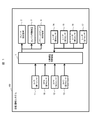
- FIG. 1 is a diagram showing a configuration example of an automatic driving system provided in a vehicle to which the present invention is applied.
- the automatic driving system 100 includes a camera (first sensor) 11, a camera (second sensor) 12, and a camera (third), which are outside world recognition sensors for recognizing the outside world situation of the vehicle.
- Sensor 13, radar (4th sensor) 14, radar (5th sensor) 15, radar (6th sensor) 16, radar (7th sensor) 17, GPS (Global Positioning System: 8th sensor) ) Equipped with 18.
- the automatic driving system 100 includes an automatic driving control device 1, a brake control device 2, an engine control device 3, and a power steering control device 4.
- the brake control device 2, the engine control device 3, and the power steering control device 4 can be collectively referred to as an actuator control device that controls the operation of the vehicle.
- the fourth sensor 14, the fifth sensor 15, the sixth sensor 16, the seventh sensor 17, and the automatic operation control device 1, the brake control device 2, the engine control device 3, and the power steering control device 4, which are radar information, are, for example, They are connected so that they can communicate with each other by an in-vehicle network such as CAN (Controller Area Network) or Sensornet (registered trademark).
- CAN Controller Area Network
- Sensornet registered trademark
- the brake control device 2 is a control device that controls the brake of the vehicle (braking force control), and the engine control device 3 is a control device that controls the engine that generates the driving force of the vehicle. Further, the power steering control device 4 is a control device that controls the power steering of the vehicle.
- the automatic driving control device 1 when the automatic driving control device 1 receives the request for automatic driving, the automatic driving control device 1 calculates the route (track) on which the vehicle moves based on the information of the outside world such as the first sensor 11, the seventh sensor 17, and the eighth sensor 18. Then, control commands such as brakes and driving forces are output to the brake control device 2, the engine control device 3, and the power steering control device 4 so as to move the vehicle according to the calculated route.
- the brake control device 2, the engine control device 3, and the power steering control device 4 receive a control command for automatic driving control from the automatic driving control device 1 and output an operation signal to each control target (actuator).
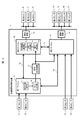
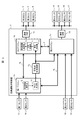
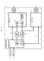
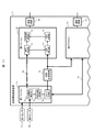
- FIG. 2 is a diagram showing an internal configuration of the automatic operation control device 1 (first ECU) in this embodiment.
- the automatic operation control device 1 (first ECU) of this embodiment includes a plurality of microcomputers (first microcomputer 1a, second microcomputer 1b, third microcomputer 1c).
- the output signals of the camera (first sensor) 11 and the GPS (eighth sensor) 18 are input to the first microcomputer 1a, and the first microcomputer 1a inputs the result of arithmetic processing to the inter-microcomputer communication line 1g or the inter-microcomputer communication line 1h. It is transmitted to the second microcomputer 1b or the third microcomputer 1c via the device.
- the output signals of the camera (second sensor) 12 and the camera (third sensor) 13 are input to the third microcomputer 1c, and the radar (fourth sensor) 14, the radar (fifth sensor) 15, and the radar (sixth sensor) 16 , And the output signal of the radar (7th sensor) 17 is input to the 3rd microcomputer 1c via the communication circuit 1d, and the 3rd microcomputer 1c calculates and processes the result to the 2nd microcomputer via the inter-microcomputer communication line 1i. It is transmitted to 1b.
- the second microcomputer 1b integrates sensor information from the processing results of the first microcomputer 1a and the third microcomputer 1c to determine the information of the outside world, calculates the route (track) on which the vehicle moves, and the brake control device (second ECU). ) 2,
- the control signal is output to the engine control device (third ECU) 3 and the power steering control device (fourth ECU) 4 via the communication circuit 1e.
- the second microcomputer 1b can extract highly accurate time information from GPS information, and can hold accurate time information inside the microcomputer.
- the automatic operation control device (first ECU) 1 includes a waveform generation circuit 1f, the first microcomputer 1a controls the reset signal of the waveform generation circuit 1f, and the output signals of the waveform generation circuit 1f are the second microcomputer 1b and the first. 3 Input to the microcomputer 1c.
- the first microcomputer 1a passes a notification of the start of reset generation synchronized with the time from the time information holding unit 1j inside the microcomputer to the reset generation unit 1k, and the reset generation unit 1k generates a reset signal and outputs it to the waveform generation circuit 1f. ..
- the waveform generation circuit 1f generates a waveform in which the voltage fluctuates at regular intervals after the reset is released and the time and the voltage have a corresponding relationship.
- the waveform generation circuit 1f uses the input reset signal to release the reset state inside the waveform generation circuit 1f, and starts waveform generation and signal output. As a result, the start of waveform generation is synchronized with the time inside the microcomputer.
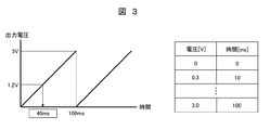
- FIG. 3 is a diagram showing an example of the relationship between the voltage and time of the output signal of the waveform generation circuit 1f in this embodiment.
- FIG. 3 shows a sawtooth wave having an amplitude of 3 V and a period of 100 ms.
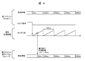
- FIG. 4 is a sequence diagram showing a time synchronization method in this embodiment.
- the second microcomputer 1b acquires the voltage of the signal waveform by the internal voltage detection unit 1m at an arbitrary timing.
- the time conversion unit 1n converts the voltage into time by having either a correspondence table showing the correspondence between voltage and time as shown in FIG. 3 or a calculation formula showing the correspondence between voltage and time. Convert.
- the time information holding unit 1o compares the time information held inside the microcomputer with the time acquired by the time conversion unit 1n, and corrects the time inside the microcomputer.
- a sawtooth wave is shown in FIG. 3, it does not have to be a sawtooth wave as long as the waveform has a one-to-one correspondence between voltages at regular intervals.
- the third microcomputer 1c can be equipped with a voltage detection unit, a time conversion unit, and a time information holding unit to synchronize the time.
- the electronic control device of this embodiment includes a plurality of microcomputers (first microcomputer 1a, second microcomputer 1b, third microcomputer 1c) and a plurality of microcomputers (first microcomputer 1a, second microcomputer 1b, Of the third microcomputer 1c), the waveform generation circuit 1f connected between the master microcomputer (first microcomputer 1a) that is the time synchronization source and the slave microcomputer (second microcomputer 1b, third microcomputer 1c) that performs time synchronization.
- the master microcomputer (first microcomputer 1a) outputs a reset signal synchronized with the time to the waveform generation circuit 1f, and the waveform generation circuit 1f corresponds to the time change of the master microcomputer (first microcomputer 1a).
- the waveform signal is output to the slave microcomputer (second microcomputer 1b, third microcomputer 1c), and the slave microcomputer (second microcomputer 1b, third microcomputer 1c) measures the voltage value of the waveform signal and uses the measured voltage value as the measured voltage value. Detect the corresponding time.
- the waveform generation circuit 1f changes the voltage in a fixed cycle after the reset is released by the reset signal, and outputs a waveform signal (saw wave) in which the time in one cycle and the voltage value have a one-to-one correspondence, and the slave microcomputer (slave microcomputer).
- the second microcomputer 1b and the third microcomputer 1c) capture the voltage value of the waveform signal (saw wave) of the waveform generation circuit 1f, and calculate the time from the captured voltage value.
- FIG. 5 is a diagram showing an internal configuration of the automatic operation control device 1 (first ECU) in this embodiment.
- the automatic operation control device 1 of this embodiment is provided with a sine wave generation circuit 1p and a PWM generation unit 1q in place of the waveform generation circuit 1f and the reset generation unit 1k of the first embodiment (FIG. 2). It is different from 1 (Fig. 2).
- Other configurations are the same as those in the first embodiment (FIG. 2).
- a sine wave is generated using the PWM function of the microcomputer to synchronize the time.
- the first microcomputer 1a passes a notification of the start of PWM generation synchronized with the time from the time information holding unit 1j inside the microcomputer to the PWM generation unit 1q, and the PWM generation unit 1q generates a PWM signal and outputs it to the sine wave generation circuit 1p. do.
- the sine wave generation circuit 1p uses the input PWM signal to output a sine wave corresponding to the voltage and period of the PWM signal.
- FIG. 6 is a diagram showing an example of the relationship between the voltage and time of the output signal of the sine wave generation circuit 1p in this embodiment.
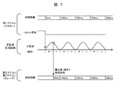
- the sine wave signal Since the sine wave signal has the same voltage twice in one cycle, it is judged in combination with the slope of the sine wave signal. Obtain the voltage value twice in a row within a short time with respect to the period of the sinusoidal signal (V 1 and V 2 ), and subtract the first voltage from the second voltage (V 2- V 1 ). Can be determined, and the time can be obtained from the voltage value and gradient of the sine wave signal.
- FIG. 7 is a sequence diagram showing a time synchronization method in this embodiment.
- the second microcomputer 1b acquires the voltage of the signal waveform from the internal voltage detection unit 1m at an arbitrary timing.
- the time conversion unit 1n converts voltage into time by having either a correspondence table showing the correspondence between voltage and time as shown in FIG. 6 or a calculation formula showing the correspondence between voltage and time. do.
- the time information holding unit 1o compares the time information held inside the microcomputer with the time acquired by the time conversion unit 1n, and corrects the time inside the microcomputer.
- the waveform generation circuit changes the voltage at regular intervals after the reset signal is released, and the voltage value and the waveform gradient are used.
- a waveform signal (sine wave signal) corresponding to the time in one cycle is output, and the slave microcomputer (second microcomputer 1b, third microcomputer 1c) is a waveform signal (sine wave generation circuit 1p) of the waveform generation circuit (sine wave generation circuit 1p).
- the voltage value of the sine wave signal) is taken in, and the time is calculated from the taken-in voltage value.
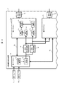
- FIG. 8 is a diagram showing an internal configuration of the automatic operation control device 1 (first ECU) in this embodiment.
- the automatic operation control device 1 of the present embodiment is implemented in that it includes a plurality of waveform generation circuits 1f, a voltage detection unit 1m, and a time conversion unit 1n (here, two each) of the first embodiment (FIG. 2). It is different from Example 1 (Fig. 2). Other configurations are the same as those in the first embodiment (FIG. 2).
- time synchronization is performed using a plurality of waveform generation circuits 1f and 1r having different cycles.
- the waveform generation circuit 1f shown in the first embodiment and the waveform generation circuit 1r having a different period are provided, a reset signal output from the first microcomputer 1a is input, and a waveform signal is input to the second microcomputer 1b and the third microcomputer 1c. Is output.
- the waveform generation circuit 1r, the voltage detection unit 1s, and the time conversion unit 1t are connected in parallel with the waveform generation circuit 1f, the voltage detection unit 1m, and the time conversion unit 1n between the reset generation unit 1k and the time information holding unit 1o. ..
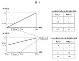
- FIG. 9 is a diagram showing an example of the relationship between the voltage and time of the output signals of the waveform generation circuits 1f and 1r in this embodiment. The correspondence between the voltage and time of two types of sawtooth waves having an amplitude of 3 V and a period of 100 ms and an amplitude of 3 V and a period of 10 ms is shown.
- a waveform with a slow cycle can estimate a long time, but the accuracy of the acquired voltage is required to estimate the time correctly. Moreover, although a waveform with a fast cycle can be estimated only at a short time, voltage accuracy is not so necessary. By acquiring the voltage of the waveforms having different cycles, it is possible to acquire the time with high accuracy without requiring high voltage resolution.
- the second microcomputer 1b acquires the voltage of the signal waveform from the internal voltage detection units 1m and 1s at an arbitrary timing.
- the time conversion units 1n and 1t change the voltage into time by having either a correspondence table showing the correspondence between voltage and time as shown in FIG. 9 or a calculation formula showing the correspondence between voltage and time. Convert to.
- the time information holding unit 1o compares the time information held inside the microcomputer with the time acquired by the time conversion units 1n and 1t, and corrects the time inside the microcomputer.
- the waveform generation circuits 1f and 1r are configured by connecting a plurality of circuits that output waveform signals having different periods in parallel.
- the time can be synchronized by combining the voltage values of a plurality of waveform signals, and the voltage detectors 1m and 1s, which are AD converters mounted on the slave microcomputers (second microcomputer 1b and third microcomputer 1c), can be synchronized.
- the accuracy of time synchronization between microcomputers can be improved without depending on the accuracy.
- FIG. 10 is a diagram showing an internal configuration of the automatic operation control device 1 (first ECU) in this embodiment.
- the automatic operation control device 1 of the present embodiment includes a communication control unit 1v, a communication circuit 1u, and a communication control unit 1w in place of the time information holding unit 1j and the time information holding unit 1o of the first embodiment (FIG. 2). In that respect, it is different from Example 1 (FIG. 2).
- Other configurations are the same as those in the first embodiment (FIG. 2).
- the delay of the communication circuit is measured using the waveform generation circuit 1f.
- a communication circuit 1u having a delay like an Ethernet Switch is provided between the first microcomputer 1a and the second microcomputer 1b.
- the communication control unit 1v inside the first microcomputer 1a passes a notification of the start of reset generation to the reset generation unit 1k.
- the reset generation unit 1k generates a reset signal and outputs it to the waveform generation circuit 1f.
- the communication control unit 1w of the second microcomputer 1b passes a notification to the voltage detection unit 1m at the timing when reception is completed, and the voltage detection unit 1m acquires the voltage of the signal waveform.
- the time conversion unit 1n converts the acquired voltage into time. This time is the communication delay from the start of transmission of the first microcomputer 1a to the completion of reception of the second microcomputer 1b.
- the electronic control device of this embodiment has a communication interface (communication line 1g between microcomputers, communication circuit) between a master microcomputer (first microcomputer 1a) and a slave microcomputer (second microcomputer 1b, third microcomputer 1c). 1u) is provided, and the master microcomputer (first microcomputer 1a) transmits information to a slave microcomputer (second microcomputer 1b, third microcomputer 1c) via a communication interface (communication line between microcomputers 1g, communication circuit 1u).
- the reset signal of the waveform generation circuit 1f is released, and the slave microcomputers (second microcomputer 1b, third microcomputer 1c) receive the information and at the same time acquire the voltage value of the waveform signal of the waveform generation circuit 1f.
- the delay time of the communication interface (communication line 1g between microcomputers, communication circuit 1u) is measured from the time corresponding to the acquired voltage value.
- FIG. 11 is a diagram showing an internal configuration of the automatic operation control device 1 (first ECU) in this embodiment.
- the automatic operation control device 1 of the present embodiment is different from the first embodiment (FIG. 2) in that it further includes a time information extraction unit 1y and a communication control unit 1x in addition to the configuration of the first embodiment (FIG. 2). It's different. Other configurations are the same as those in the first embodiment (FIG. 2).
- the time information acquired by GPS or the like using the waveform generation circuit 1f is shared between the microcomputers.
- the first microcomputer 1a calculates accurate time information by the time information extraction unit 1y and passes the signal input from the GPS (eighth sensor) 18 or the like to the time information holding unit 1j.
- the time information holding unit 1j transmits the time information to the second microcomputer 1b via the communication line 1g between the microcomputers, and at the same time, passes a notification of the start of reset generation to the reset generation unit 1k, and the reset generation unit 1k generates a reset signal. , Output to the waveform generation circuit 1f.
- the waveform generation circuit 1f generates a waveform in which the voltage fluctuates at regular intervals after the reset is released and the time and the voltage have a corresponding relationship.
- FIG. 12 is a sequence diagram showing a time sharing method in this embodiment.
- the communication control unit 1x of the second microcomputer 1b receives the communication signal from the first microcomputer 1a and at the same time notifies the voltage detection unit 1m, and the voltage detection unit 1m acquires the voltage of the signal waveform. Further, the communication control unit 1x extracts the time information from the received signal and passes the time information to the time information holding unit 1o.
- the time conversion unit 1n converts voltage into time by having either a correspondence table showing the correspondence between voltage and time as shown in FIG. 3 or a calculation formula showing the correspondence between voltage and time. do.
- the time information holding unit 1o compares the time information passed from the communication control unit 1x with the communication delay acquired by the time conversion unit 1n, and corrects the delay due to communication.
- the master microcomputer (first microcomputer 1a) is a slave microcomputer (second microcomputer 1b, third microcomputer 1c) via a communication interface (communication line between microcomputers 1g).
- the slave microcomputers receive the time information and at the same time, the voltage of the waveform signal of the waveform generation circuit 1f. The value is acquired, and the received time information is corrected based on the time corresponding to the acquired voltage value.
- Serial communication is generally used for communication between microcomputers (communication line between microcomputers 1 g), but since serial communication causes a communication delay, accurate time information cannot be transmitted. Therefore, as in this embodiment, time synchronization with low delay can be realized by time correction using the waveform signal from the waveform generation circuit 1f.
- the electronic control device of this embodiment is provided with a communication interface (communication line between microcomputers 1g) between the master microcomputer (first microcomputer 1a) and the slave microcomputers (second microcomputer 1b, third microcomputer 1c), and is a master.
- the microcomputer (first microcomputer 1a) acquires time information by GPS and transmits the acquired time information to slave microcomputers (second microcomputer 1b, third microcomputer 1c) via a communication interface (communication line between microcomputers 1g).
- the reset signal of the waveform generation circuit 1f is released, and the slave microcomputers (second microcomputer 1b, third microcomputer 1c) receive the time information and at the same time acquire the voltage value of the waveform signal of the waveform generation circuit 1f.
- the time corresponding to the acquired voltage value and the time information acquired by GPS are compared, and the delay time due to the communication interface (communication line between microcomputers 1g) is corrected based on the comparison result.
- the time information acquired by GPS can be shared between the microcomputers, and the accuracy of time synchronization between the microcomputers can be improved.
- the present invention is not limited to the above-described embodiment, but includes various modifications.
- the above embodiments have been described in detail to aid in understanding of the present invention and are not necessarily limited to those comprising all of the described configurations.
- it is possible to replace a part of the configuration of one embodiment with the configuration of another embodiment and it is also possible to add the configuration of another embodiment to the configuration of one embodiment.
Landscapes
- Engineering & Computer Science (AREA)
- Theoretical Computer Science (AREA)
- Physics & Mathematics (AREA)
- General Physics & Mathematics (AREA)
- General Engineering & Computer Science (AREA)
- Synchronisation In Digital Transmission Systems (AREA)
- Combined Controls Of Internal Combustion Engines (AREA)
Abstract
複数のマイコンを使用して分散処理を行う電子制御装置において、各マイコンの演算処理を阻害することなく、遅延の少ない高精度なマイコン間の時刻同期が可能な電子制御装置を提供する。複数のマイコンと、前記複数のマイコンのうち、時刻同期元となるマスターマイコンと時刻同期を行うスレーブマイコンとの間に接続された波形生成回路と、を備え、前記マスターマイコンは、時刻に同期したリセット信号を前記波形生成回路へ出力し、前記波形生成回路は、前記マスターマイコンの時刻変化に対応した波形信号を前記スレーブマイコンへ出力し、前記スレーブマイコンは、前記波形信号の電圧値を測定し、当該測定した電圧値に対応する時刻を検出することを特徴とする。
Description
本発明は、電子制御装置の構成とその制御に係り、特に、自動運転システムのような高信頼かつ高精度な制御が要求される電子制御装置に適用して有効な技術に関する。
自動運転を制御する電子制御装置(ECU:Electronic Control Unit)には、外界認識の処理を行う演算処理装置(マイコン)が実装されているが、必要な処理性能の増大により複数のマイコンを使用して分散処理する場合がある。分散処理を行う場合、各マイコンが同期して処理をする必要があり、同期処理をするためにマイコン間の時刻を同期させる必要がある。
一般的に、マイコン間で時刻を同期する手法としてシリアル通信などを利用して時刻情報をやり取りする方法がある。同期元となるマスターマイコンから、時刻情報を含む通信フレームを受信先となるスレーブマイコンへ伝送し、スレーブマイコンは受け取った通信フレームから時刻情報を取り出し、スレーブマイコン内部の時刻を補正する。
本技術分野の背景技術として、例えば、特許文献1のような技術がある。特許文献1には「通信フレームの受信開始と同時に割込み機能を有効にしてタイマカウンタをセットし、タイマカウンタで受信フレーム処理にかかる遅延時間を計測し、フレーム処理遅延を除去する手法」が開示されている。
代表的な自動運転システムは、例えば、車両の周囲の状況を把握するための多数のセンサと、制御指令を出力する車両制御装置と、車両制御装置からの制御指令に基づいてエンジン制御やブレーキ制御、パワーステアリング制御などをそれぞれに実施する複数のアクチュエータ制御装置で構成される。
ここで、自動運転システムの車両制御装置は自動運転を実現するために高い演算能力が必要であり、高性能の演算処理装置で構成されている。自動運転レベルが上がるにつれて、必要とされるセンサ数や演算処理が増えるため、演算処理装置を複数使用し、別々の演算処理装置にセンサを接続する場合がある。このような場合、複数の演算処理装置で同じ時刻で処理を実行しないと各センサ信号の情報を正しく統合できない。そのため、演算処理装置間において高い精度で時刻同期を行う必要がある。
演算処理装置間の時刻同期に上記特許文献1の方式を用いる場合、演算処理装置の割込み機能を使用する必要がある。
割込み機能を使用する場合、演算処理装置に搭載されているOS(Operating System)の割込み優先度により、割込み機能が有効になるまでの時間が異なる。また、割込み処理により、自動運転のための演算処理が中断される可能性があり、その結果、演算処理時間が増えて処理が間に合わなくなる懸念がある。
また、特許文献1の方式は受信処理にかかる遅延は除去できるが、送信処理による遅延は除去できない。したがって、自動運転のような精度の高い時刻同期が必要なシステムでは遅延が問題になる可能性がある。
そこで、本発明の目的は、複数のマイコンを使用して分散処理を行う電子制御装置において、各マイコンの演算処理を阻害することなく、遅延の少ない高精度なマイコン間の時刻同期が可能な電子制御装置を提供することにある。
上記課題を解決するために、本発明は、複数のマイコンと、前記複数のマイコンのうち、時刻同期元となるマスターマイコンと時刻同期を行うスレーブマイコンとの間に接続された波形生成回路と、を備え、前記マスターマイコンは、時刻に同期したリセット信号を前記波形生成回路へ出力し、前記波形生成回路は、前記マスターマイコンの時刻変化に対応した波形信号を前記スレーブマイコンへ出力し、前記スレーブマイコンは、前記波形信号の電圧値を測定し、当該測定した電圧値に対応する時刻を検出することを特徴とする。
本発明によれば、複数のマイコンを使用して分散処理を行う電子制御装置において、各マイコンの演算処理を阻害することなく、遅延の少ない高精度なマイコン間の時刻同期が可能な電子制御装置を提供することができる。
これにより、高信頼かつ高精度な電子制御装置及びそれを用いた自動運転システムを実現することができる。
上記した以外の課題、構成及び効果は、以下の実施形態の説明により明らかにされる。
以下、図面を用いて本発明の実施例を説明する。なお、各図面において同一の構成については同一の符号を付し、重複する部分についてはその詳細な説明は省略する。
≪自動運転システムの構成例≫
先ず、図1を参照して、本発明が適用される自動運転システム(車両制御システム)の構成について説明する。
先ず、図1を参照して、本発明が適用される自動運転システム(車両制御システム)の構成について説明する。
図1は、本発明が適用される車両に備えられる自動運転システムの構成例を示す図である。図1に示すように、自動運転システム100は、車両の外界状況を認識するための外界認識センサである、カメラ(第1センサ)11と、カメラ(第2センサ)12と、カメラ(第3センサ)13と、レーダ(第4センサ)14と、レーダ(第5センサ)15と、レーダ(第6センサ)16と、レーダ(第7センサ)17と、GPS(Global Positioning System:第8センサ)18を備えている。
また、自動運転システム100は、自動運転制御装置1と、ブレーキ制御装置2と、エンジン制御装置3と、パワーステアリング制御装置4を備えている。なお、ブレーキ制御装置2、エンジン制御装置3、及びパワーステアリング制御装置4は、車両の動作を制御するアクチュエータ制御装置と総称することができる。
レーダ情報である第4センサ14、第5センサ15、第6センサ16、第7センサ17、及び自動運転制御装置1、ブレーキ制御装置2、エンジン制御装置3、パワーステアリング制御装置4は、例えば、CAN(Controller Area Network:コントローラエリアネットワーク)やEthernet(登録商標)等の車載ネットワークによって相互に通信可能となるよう接続される。
ブレーキ制御装置2は、車両のブレーキ制御(制動力制御)を行う制御装置であり、エンジン制御装置3は、車両の駆動力を発生するエンジンを制御する制御装置である。また、パワーステアリング制御装置4は、車両のパワーステアリングを制御する制御装置である。
ここで、自動運転制御装置1は、自動運転の要求を受け付けると、第1センサ11から第7センサ17、第8センサ18等の外界の情報を基に車両が移動するルート(軌道)を算出し、算出したルート通りに車両を移動させるように、ブレーキや駆動力などの制御指令を、ブレーキ制御装置2、エンジン制御装置3、及びパワーステアリング制御装置4に出力する。
ブレーキ制御装置2、エンジン制御装置3、パワーステアリング制御装置4は、自動運転制御装置1から自動走行制御の制御指令を受けて、各制御対象(アクチュエータ)に操作信号を出力する。
次に、図2から図4を参照して、本発明の実施例1に係る自動運転制御装置1の構成と動作(制御)について説明する。
図2は、本実施例における自動運転制御装置1(第1ECU)の内部構成を示す図である。
図2に示すように、本実施例の自動運転制御装置1(第1ECU)は、複数のマイコン(第1マイコン1a,第2マイコン1b,第3マイコン1c)を備えている。カメラ(第1センサ)11及びGPS(第8センサ)18の出力信号は第1マイコン1aへ入力され、第1マイコン1aは演算処理した結果を、マイコン間通信線路1gまたはマイコン間通信線路1hを介して、第2マイコン1bまたは第3マイコン1cへ伝送する。
カメラ(第2センサ)12及びカメラ(第3センサ)13の出力信号は第3マイコン1cへ入力され、レーダ(第4センサ)14、レーダ(第5センサ)15、レーダ(第6センサ)16、及びレーダ(第7センサ)17の出力信号は通信回路1dを介して第3マイコン1cへ入力され、第3マイコン1cは演算処理した結果を、マイコン間通信線路1iを介して、第2マイコン1bへ伝送する。
第2マイコン1bは、第1マイコン1a及び第3マイコン1cの処理結果よりセンサ情報を統合して外界の情報を判別し、車両が移動するルート(軌道)を算出し、ブレーキ制御装置(第2ECU)2、エンジン制御装置(第3ECU)3、パワーステアリング制御装置(第4ECU)4へ、通信回路1eを介して制御信号を出力する。
第2マイコン1bは、GPS情報から高精度の時刻情報を抽出することができ、マイコン内部で正確な時刻情報を保持することができる。
また、自動運転制御装置(第1ECU)1は、波形生成回路1fを備え、第1マイコン1aは波形生成回路1fのリセット信号を制御し、波形生成回路1fの出力信号は第2マイコン1b及び第3マイコン1cに入力される。
第1マイコン1aは、マイコン内部の時刻情報保持部1jから時刻に同期したリセット生成開始の通知をリセット生成部1kに渡し、リセット生成部1kはリセット信号を生成し、波形生成回路1fへ出力する。
波形生成回路1fは、リセット解除後、一定の周期で電圧変動し、時間と電圧は対応関係を持つような波形を生成する。
波形生成回路1fは入力されるリセット信号を用いて、波形生成回路1f内部のリセット状態を解除し、波形生成及び信号出力を開始する。これにより、波形生成開始がマイコン内部の時刻と同期する。
図3は、本実施例における波形生成回路1fの出力信号の電圧と時間の関係の一例を示す図である。
一定の周期で電圧と時間が一対一対応する波形としてのこぎり波がある。図3では振幅3V,周期100msとなるのこぎり波を示している。このように一定の周期で一対一対応する波形で、かつ、波形の振幅および周期が既知であれば、信号波形の電圧値より時間が求めることが可能である。
図4は、本実施例における時刻同期方法を示すシーケンス図である。
第2マイコン1bは、任意のタイミングで、内部の電圧検出部1mで信号波形の電圧を取得する。
時刻変換部1nは、図3に示すような、電圧と時間の対応関係を示した対応表、もしくは、電圧と時間の対応関係を示した計算式のいずれかを持つことにより、電圧を時間に変換する。
時刻情報保持部1oは、マイコン内部で保持していた時刻情報と、時刻変換部1nで取得した時刻を比較し、マイコン内部の時刻を補正する。
なお、図3にはのこぎり波を示しているが、一定の周期で電圧が一対一対応する波形であれば、のこぎり波でなくてもかまわない。
また、第3マイコン1cについても第2マイコン1bと同様に、電圧検出部、時刻変換部、時刻情報保持部を実装し、時刻同期をすることが可能である。
以上説明したように、本実施例の電子制御装置は、複数のマイコン(第1マイコン1a,第2マイコン1b,第3マイコン1c)と、複数のマイコン(第1マイコン1a,第2マイコン1b,第3マイコン1c)のうち、時刻同期元となるマスターマイコン(第1マイコン1a)と時刻同期を行うスレーブマイコン(第2マイコン1b,第3マイコン1c)との間に接続された波形生成回路1fを備えており、マスターマイコン(第1マイコン1a)は、時刻に同期したリセット信号を波形生成回路1fへ出力し、波形生成回路1fは、マスターマイコン(第1マイコン1a)の時刻変化に対応した波形信号をスレーブマイコン(第2マイコン1b,第3マイコン1c)へ出力し、スレーブマイコン(第2マイコン1b,第3マイコン1c)は、波形信号の電圧値を測定し、当該測定した電圧値に対応する時刻を検出する。
これにより、マイコン間の時刻同期を比較的簡単な回路構成で実現することができる。
また、波形生成回路1fは、リセット信号でリセット解除後に、一定の周期で電圧を変化させ、一周期内の時間と電圧値が一対一対応する波形信号(のこぎり波)を出力し、スレーブマイコン(第2マイコン1b,第3マイコン1c)は、波形生成回路1fの波形信号(のこぎり波)の電圧値を取り込み、当該取り込んだ電圧値から時刻を算出する。
これにより、時刻と電圧を一対一対応させることができ、経過時刻を容易に計算することができる。
図5から図7を参照して、本発明の実施例2に係る自動運転制御装置1の構成と動作(制御)について説明する。
図5は、本実施例における自動運転制御装置1(第1ECU)の内部構成を示す図である。本実施例の自動運転制御装置1は、実施例1(図2)の波形生成回路1f及びリセット生成部1kに替えて、正弦波生成回路1p及びPWM生成部1qを備えている点において実施例1(図2)とは異なっている。その他の構成は実施例1(図2)と同様である。
本実施例では、マイコンのPWM機能を用いて正弦波を生成し、時刻同期を行う。第1マイコン1aは、マイコン内部の時刻情報保持部1jから時刻に同期したPWM生成開始の通知をPWM生成部1qに渡し、PWM生成部1qはPWM信号を生成し、正弦波生成回路1pへ出力する。
正弦波生成回路1pは、入力されるPWM信号を用いて、PWM信号の電圧及び周期に対応した正弦波を出力する。
図6は、本実施例における正弦波生成回路1pの出力信号の電圧と時間の関係の一例を示す図である。
正弦波信号は1周期で2回同じ電圧になるため、正弦波信号の傾きと組合せて判断する。正弦波信号の周期に対して短い時間内に2回連続で電圧値を取得し(V1及びV2)、2回目の電圧から1回目の電圧を引くこと(V2-V1)で傾きが判別でき、正弦波信号の電圧値および傾きから時間を求めることが可能である。
図7は、本実施例における時刻同期方法を示すシーケンス図である。
第2マイコン1bは、任意のタイミングで、内部の電圧検出部1mより信号波形の電圧を取得する。
時刻変換部1nは、図6に示すような、電圧と時間の対応関係を示した対応表、もしくは電圧と時間の対応関係を示した計算式のいずれかを持つことにより、電圧を時間に変換する。
時刻情報保持部1oは、マイコン内部で保持していた時刻情報と、時刻変換部1nで取得した時刻を比較し、マイコン内部の時刻を補正する。
以上説明したように、本実施例の電子制御装置では、波形生成回路(正弦波生成回路1p)は、リセット信号でリセット解除後に、一定の周期で電圧を変化させ、電圧値と波形の傾きから一周期内の時間と一対一対応する波形信号(正弦波信号)を出力し、スレーブマイコン(第2マイコン1b,第3マイコン1c)は、波形生成回路(正弦波生成回路1p)の波形信号(正弦波信号)の電圧値を取り込み、当該取り込んだ電圧値から時刻を算出する。
これにより、正弦波のような電圧から一意に時刻が定まらない波形信号を用いた場合であっても、比較的簡単な計算(波形の傾きの算出)により、経過時刻を計算することができる。
図8及び図9を参照して、本発明の実施例3に係る自動運転制御装置1の構成と動作(制御)について説明する。
図8は、本実施例における自動運転制御装置1(第1ECU)の内部構成を示す図である。本実施例の自動運転制御装置1は、実施例1(図2)の波形生成回路1f及び電圧検出部1m、時刻変換部1nを複数(ここでは、それぞれ2つずつ)備えている点において実施例1(図2)とは異なっている。その他の構成は実施例1(図2)と同様である。
本実施例では、周期の違う複数の波形生成回路1f,1rを用いて時刻同期を行う。実施例1で示した波形生成回路1fと、別の周期を持つ波形生成回路1rを備え、第1マイコン1aより出力されるリセット信号を入力し、第2マイコン1bおよび第3マイコン1cへ波形信号を出力する。波形生成回路1r,電圧検出部1s,時刻変換部1tは、リセット生成部1kと時刻情報保持部1oの間において、波形生成回路1f,電圧検出部1m,時刻変換部1nと並列に接続される。
図9は、本実施例における波形生成回路1f、1rの出力信号の電圧と時間の関係の一例を示す図である。振幅3V,周期100msと、振幅3V,周期10msとなる2種類ののこぎり波の電圧と時間の対応を示している。
周期の遅い波形は長い時刻を推定できるが、正しく時刻を推定するためには取得する電圧の精度が必要になる。また、周期の早い波形は短い時刻しか推定できないが、電圧の精度はそれほど必要ない。周期の異なる波形の電圧を取得することにより、高い電圧分解能を必要とせず、精度の高い時刻を取得することが可能となる。
第2マイコン1bは、任意のタイミングで、内部の電圧検出部1m,1sより信号波形の電圧を取得する。
時刻変換部1n,1tは、図9に示すような、電圧と時間の対応関係を示した対応表、もしくは電圧と時間の対応関係を示した計算式のいずれかを持つことにより、電圧を時間に変換する。
時刻情報保持部1oは、マイコン内部で保持していた時刻情報と、時刻変換部1n,1tで取得した時刻を組合せて比較し、マイコン内部の時刻を補正する。
以上説明したように、本実施例の電子制御装置では、波形生成回路1f,1rは、周期の異なる波形信号を出力する複数の回路が並列に接続されて構成される。
これにより、複数の波形信号の電圧値の組み合わせで時刻を同期させることができ、スレーブマイコン(第2マイコン1b,第3マイコン1c)に搭載されたAD変換器である電圧検出部1m,1sの精度に依存することなく、マイコン間の時刻同期の精度を向上することができる。
図10を参照して、本発明の実施例4に係る自動運転制御装置1の構成と動作(制御)について説明する。
図10は、本実施例における自動運転制御装置1(第1ECU)の内部構成を示す図である。本実施例の自動運転制御装置1は、実施例1(図2)の時刻情報保持部1j及び時刻情報保持部1oに替えて、通信制御部1v及び通信回路1u、通信制御部1wを備えている点において実施例1(図2)とは異なっている。その他の構成は実施例1(図2)と同様である。
本実施例では、波形生成回路1fを用いて通信回路の遅延を測定する。第1マイコン1aと第2マイコン1bの間にはEthernet Switchのような遅延を持つ通信回路1uを備えている。
マイコン間通信線路1gを介して、第1マイコン1aから第2マイコン1bへ時刻情報を送信すると同時に、第1マイコン1a内部の通信制御部1vからリセット生成部1kにリセット生成開始の通知を渡し、リセット生成部1kはリセット信号を生成し波形生成回路1fへ出力する。
第2マイコン1bの通信制御部1wは、受信完了したタイミングで、電圧検出部1mに通知を渡し、電圧検出部1mは信号波形の電圧を取得する。
時刻変換部1nは、取得した電圧を時間に変換する。この時間が第1マイコン1aの送信開始から第2マイコン1bの受信完了までの通信遅延となる。
以上説明したように、本実施例の電子制御装置は、マスターマイコン(第1マイコン1a)とスレーブマイコン(第2マイコン1b,第3マイコン1c)間に通信インターフェース(マイコン間通信線路1g,通信回路1u)を備えており、マスターマイコン(第1マイコン1a)は、通信インターフェース(マイコン間通信線路1g,通信回路1u)を介してスレーブマイコン(第2マイコン1b,第3マイコン1c)へ情報を送信すると同時に、波形生成回路1fのリセット信号を解除し、スレーブマイコン(第2マイコン1b,第3マイコン1c)は、情報を受信すると同時に、波形生成回路1fの波形信号の電圧値を取得し、当該取得した電圧値に対応する時刻から通信インターフェース(マイコン間通信線路1g,通信回路1u)の遅延時間を測定する。
これにより、マイコン間の通信インターフェースの遅延時間を正確に測定することができる。
図11及び図12を参照して、本発明の実施例5に係る自動運転制御装置1の構成と動作(制御)について説明する。
図11は、本実施例における自動運転制御装置1(第1ECU)の内部構成を示す図である。本実施例の自動運転制御装置1は、実施例1(図2)の構成に加えて、さらに時刻情報抽出部1y及び通信制御部1xを備えている点において実施例1(図2)とは異なっている。その他の構成は実施例1(図2)と同様である。
本実施例では、波形生成回路1fを用いてGPSなどで取得した時刻情報をマイコン間で共有する。第1マイコン1aはGPS(第8センサ)18などから入力される信号を時刻情報抽出部1yで正確な時刻情報を算出し、時刻情報保持部1jへ渡す。
時刻情報保持部1jは、マイコン間通信線路1gを介して第2マイコン1bへ時刻情報を送信すると同時に、リセット生成部1kにリセット生成開始の通知を渡し、リセット生成部1kはリセット信号を生成し、波形生成回路1fへ出力する。
波形生成回路1fは、リセット解除後、一定の周期で電圧変動し、時間と電圧は対応関係を持つような波形を生成する。
図12は、本実施例における時刻共有方法を示すシーケンス図である。
第2マイコン1bの通信制御部1xは第1マイコン1aより通信信号を受信すると同時に、電圧検出部1mへ通知し、電圧検出部1mは信号波形の電圧を取得する。また、通信制御部1xは受信した信号から時刻情報を抽出し、時刻情報保持部1oへ時刻情報を渡す。
時刻変換部1nは、図3に示すような、電圧と時間の対応関係を示した対応表、もしくは電圧と時間の対応関係を示した計算式のいずれかを持つことにより、電圧を時間に変換する。
時刻情報保持部1oは、通信制御部1xから渡された時刻情報と、時刻変換部1nで取得した通信遅延とを比較し、通信による遅延を補正する。
以上説明したように、本実施例の電子制御装置では、マスターマイコン(第1マイコン1a)は、通信インターフェース(マイコン間通信線路1g)を介してスレーブマイコン(第2マイコン1b,第3マイコン1c)へ時刻情報を送信すると同時に、波形生成回路1fのリセット信号を解除し、スレーブマイコン(第2マイコン1b,第3マイコン1c)は、時刻情報を受信すると同時に、波形生成回路1fの波形信号の電圧値を取得し、当該取得した電圧値に対応する時刻に基づき受信した時刻情報を補正する。
マイコン間の通信(マイコン間通信線路1g)には、一般的に、シリアル通信が用いられるが、シリアル通信は通信遅延が発生するため、正確な時刻情報を伝送することができない。そこで、本実施例のように、波形生成回路1fからの波形信号による時刻補正により、低遅延の時刻同期を実現することができる。
また、本実施例の電子制御装置は、マスターマイコン(第1マイコン1a)とスレーブマイコン(第2マイコン1b,第3マイコン1c)間に通信インターフェース(マイコン間通信線路1g)を備えており、マスターマイコン(第1マイコン1a)は、GPSにより時刻情報を取得し、通信インターフェース(マイコン間通信線路1g)を介して当該取得した時刻情報をスレーブマイコン(第2マイコン1b,第3マイコン1c)へ送信すると同時に、波形生成回路1fのリセット信号を解除し、スレーブマイコン(第2マイコン1b,第3マイコン1c)は、時刻情報を受信すると同時に、波形生成回路1fの波形信号の電圧値を取得し、当該取得した電圧値に対応する時刻とGPSにより取得した時刻情報を比較し、当該比較した結果に基づき通信インターフェース(マイコン間通信線路1g)による遅延時間を補正する。
これにより、GPSで取得した時刻情報をマイコン間で共有することができ、マイコン間の時刻同期の精度を向上することができる。
なお、本発明は上記した実施例に限定されるものではなく、様々な変形例が含まれる。例えば、上記の実施例は本発明に対する理解を助けるために詳細に説明したものであり、必ずしも説明した全ての構成を備えるものに限定されるものではない。また、ある実施例の構成の一部を他の実施例の構成に置き換えることが可能であり、また、ある実施例の構成に他の実施例の構成を加えることも可能である。また、各実施例の構成の一部について、他の構成の追加・削除・置換をすることが可能である。
1…自動運転制御装置(第1ECU)、2…ブレーキ制御装置(第2ECU)、3…エンジン制御装置(第3ECU)、4…パワーステアリング制御装置(第4ECU)、11…カメラ(第1センサ)、12…カメラ(第2センサ)、13…カメラ(第3センサ)、14…レーダ(第4センサ)、15…レーダ(第5センサ)、16…レーダ(第6センサ)、17…レーダ(第7センサ)、18…GPS(第8センサ)、100…自動運転システム、1a…第1マイコン、1b…第2マイコン、1c…第3マイコン、1d,1e…通信回路、1f…波形生成回路、1g,1h,1i…マイコン間通信線路、1j…時刻情報保持部、1k…リセット生成部、1m…電圧検出部、1n…時刻変換部、1o…時刻情報保持部、1p…正弦波生成回路、1q…PWM生成部、1r…波形生成回路、1s…電圧検出部、1t…時刻変換部、1u…通信回路、1v,1w,1x…通信制御部、1y…時刻情報抽出部
Claims (11)
- 複数のマイコンと、
前記複数のマイコンのうち、時刻同期元となるマスターマイコンと時刻同期を行うスレーブマイコンとの間に接続された波形生成回路と、を備え、
前記マスターマイコンは、時刻に同期したリセット信号を前記波形生成回路へ出力し、
前記波形生成回路は、前記マスターマイコンの時刻変化に対応した波形信号を前記スレーブマイコンへ出力し、
前記スレーブマイコンは、前記波形信号の電圧値を測定し、当該測定した電圧値に対応する時刻を検出する電子制御装置。 - 請求項1に記載の電子制御装置であって、
前記波形生成回路は、前記リセット信号でリセット解除後に、一定の周期で電圧を変化させ、一周期内の時間と電圧値が一対一対応する波形信号を出力し、
前記スレーブマイコンは、前記波形生成回路の波形信号の電圧値を取り込み、当該取り込んだ電圧値から時刻を算出する電子制御装置。 - 請求項1に記載の電子制御装置であって、
前記波形生成回路は、前記リセット信号でリセット解除後に、一定の周期で電圧を変化させ、電圧値と波形の傾きから一周期内の時間と一対一対応する波形信号を出力し、
前記スレーブマイコンは、前記波形生成回路の波形信号の電圧値を取り込み、当該取り込んだ電圧値から時刻を算出する電子制御装置。 - 請求項2または3に記載の電子制御装置であって、
前記波形生成回路は、周期の異なる波形信号を出力する複数の回路が並列に接続されて構成される電子制御装置。 - 請求項2または3に記載の電子制御装置であって、
前記マスターマイコンと前記スレーブマイコン間に通信インターフェースを備え、
前記マスターマイコンは、前記通信インターフェースを介して前記スレーブマイコンへ情報を送信すると同時に、前記波形生成回路のリセット信号を解除し、
前記スレーブマイコンは、前記情報を受信すると同時に、前記波形生成回路の波形信号の電圧値を取得し、当該取得した電圧値に対応する時刻から前記通信インターフェースの遅延時間を測定する電子制御装置。 - 請求項5に記載の電子制御装置であって、
前記マスターマイコンは、前記通信インターフェースを介して前記スレーブマイコンへ時刻情報を送信すると同時に、前記波形生成回路のリセット信号を解除し、
前記スレーブマイコンは、前記時刻情報を受信すると同時に、前記波形生成回路の波形信号の電圧値を取得し、当該取得した電圧値に対応する時刻に基づき受信した前記時刻情報を補正する電子制御装置。 - 請求項1に記載の電子制御装置であって、
前記マスターマイコンと前記スレーブマイコン間に通信インターフェースを備え、
前記マスターマイコンは、GPSにより時刻情報を取得し、前記通信インターフェースを介して当該取得した時刻情報を前記スレーブマイコンへ送信すると同時に、前記波形生成回路のリセット信号を解除し、
前記スレーブマイコンは、前記時刻情報を受信すると同時に、前記波形生成回路の波形信号の電圧値を取得し、当該取得した電圧値に対応する時刻と前記GPSにより取得した時刻情報を比較し、当該比較した結果に基づき前記通信インターフェースによる遅延時間を補正する電子制御装置。 - 請求項1に記載の電子制御装置であって、
前記スレーブマイコンは、電圧と時間の対応関係を示した対応表または電圧と時間の対応関係を示した計算式を有し、
前記対応表または前記計算式に基づき、前記測定した電圧値に対応する時刻を算出する電子制御装置。 - 請求項1に記載の電子制御装置であって、
前記波形生成回路は、一周期内の時間と電圧値が一対一対応するのこぎり波を出力する電子制御装置。 - 請求項1に記載の電子制御装置であって、
前記マスターマイコンは、時刻に同期したPWM信号を前記波形生成回路へ出力し、
前記波形生成回路は、前記PWM信号に基づき電圧及び周期に対応した正弦波信号を前記スレーブマイコンへ出力し、
前記スレーブマイコンは、前記正弦波信号の電圧値を測定し、当該測定した電圧値と前記正弦波信号の傾きから時刻を算出する電子制御装置。 - 請求項1から10のいずれか1項に記載の電子制御装置であって、
自動運転システムに搭載される自動運転制御装置である電子制御装置。
Priority Applications (3)
| Application Number | Priority Date | Filing Date | Title |
|---|---|---|---|
| JP2022534914A JP7314415B2 (ja) | 2020-07-06 | 2021-04-16 | 電子制御装置 |
| US18/013,784 US12045082B2 (en) | 2020-07-06 | 2021-04-16 | Electronic control device |
| DE112021002693.3T DE112021002693T5 (de) | 2020-07-06 | 2021-04-16 | Elektronische steuervorrichtung |
Applications Claiming Priority (2)
| Application Number | Priority Date | Filing Date | Title |
|---|---|---|---|
| JP2020-116119 | 2020-07-06 | ||
| JP2020116119 | 2020-07-06 |
Publications (1)
| Publication Number | Publication Date |
|---|---|
| WO2022009497A1 true WO2022009497A1 (ja) | 2022-01-13 |
Family
ID=79552884
Family Applications (1)
| Application Number | Title | Priority Date | Filing Date |
|---|---|---|---|
| PCT/JP2021/015725 Ceased WO2022009497A1 (ja) | 2020-07-06 | 2021-04-16 | 電子制御装置 |
Country Status (4)
| Country | Link |
|---|---|
| US (1) | US12045082B2 (ja) |
| JP (1) | JP7314415B2 (ja) |
| DE (1) | DE112021002693T5 (ja) |
| WO (1) | WO2022009497A1 (ja) |
Citations (3)
| Publication number | Priority date | Publication date | Assignee | Title |
|---|---|---|---|---|
| JP2001016210A (ja) * | 1999-06-25 | 2001-01-19 | Sony Corp | 通信装置および方法、並びに媒体 |
| JP2004234098A (ja) * | 2003-01-28 | 2004-08-19 | Denso Corp | 時刻同期システム |
| JP6494018B2 (ja) * | 2014-12-25 | 2019-04-03 | 株式会社日立国際電気 | 伝送装置および伝送システム |
Family Cites Families (4)
| Publication number | Priority date | Publication date | Assignee | Title |
|---|---|---|---|---|
| JPH0194018A (ja) | 1987-10-07 | 1989-04-12 | Mazda Motor Corp | 自動車の空調装置 |
| JP2001162101A (ja) | 1999-12-13 | 2001-06-19 | Tokyo Gas Co Ltd | 蒸留用コンデンサ及び蒸留塔 |
| CN110678375B (zh) * | 2017-06-05 | 2022-09-16 | 日立安斯泰莫株式会社 | 车辆控制装置及车辆控制系统 |
| JP6802391B2 (ja) * | 2017-12-25 | 2020-12-16 | 日立オートモティブシステムズ株式会社 | 車両制御装置および電子制御システム |
-
2021
- 2021-04-16 US US18/013,784 patent/US12045082B2/en active Active
- 2021-04-16 WO PCT/JP2021/015725 patent/WO2022009497A1/ja not_active Ceased
- 2021-04-16 DE DE112021002693.3T patent/DE112021002693T5/de active Pending
- 2021-04-16 JP JP2022534914A patent/JP7314415B2/ja active Active
Patent Citations (3)
| Publication number | Priority date | Publication date | Assignee | Title |
|---|---|---|---|---|
| JP2001016210A (ja) * | 1999-06-25 | 2001-01-19 | Sony Corp | 通信装置および方法、並びに媒体 |
| JP2004234098A (ja) * | 2003-01-28 | 2004-08-19 | Denso Corp | 時刻同期システム |
| JP6494018B2 (ja) * | 2014-12-25 | 2019-04-03 | 株式会社日立国際電気 | 伝送装置および伝送システム |
Also Published As
| Publication number | Publication date |
|---|---|
| US12045082B2 (en) | 2024-07-23 |
| DE112021002693T5 (de) | 2023-03-09 |
| JP7314415B2 (ja) | 2023-07-25 |
| JPWO2022009497A1 (ja) | 2022-01-13 |
| US20230288954A1 (en) | 2023-09-14 |
Similar Documents
| Publication | Publication Date | Title |
|---|---|---|
| CN110329273B (zh) | 一种用于无人驾驶获取数据同步的方法及装置 | |
| US11136044B2 (en) | Vehicle control device | |
| JP2023001121A (ja) | 電池監視システム | |
| JP5338751B2 (ja) | Pwm通信システム | |
| US9857203B2 (en) | Resolver device | |
| CN110217178B (zh) | 一种基于硬件同步的无人驾驶感知系统及其工作方法 | |
| US9182783B2 (en) | Synchronization apparatus and field device | |
| EP1684531A2 (en) | Vehicle mounted stereo camera apparatus | |
| WO2012169687A1 (ko) | 듀얼 컨트롤러 시스템의 오류 검출 장치 및 방법 | |
| US10044494B2 (en) | Electronic control device | |
| US20100154540A1 (en) | Sensor device | |
| JP7314415B2 (ja) | 電子制御装置 | |
| KR101619628B1 (ko) | 차량 내 전자장치간의 데이터 동기화 방법 | |
| US10225171B2 (en) | Assigning time stamps to received data packets | |
| CN107666360B (zh) | 列车系统时间同步控制方法和装置 | |
| CN107003152A (zh) | 用于处理机动车中的测量信号的信号处理设备 | |
| JP2018106513A (ja) | 検出装置 | |
| JP6871073B2 (ja) | 電子制御装置 | |
| WO2016142994A1 (ja) | データ収集システム | |
| JP4363444B2 (ja) | ネットワーク | |
| EP4579194B1 (en) | Sensor device for safety critical applications | |
| JP7781387B2 (ja) | 振動検出システム | |
| CN117715168B (zh) | 信号同步系统及方法 | |
| US12174691B2 (en) | Semiconductor device with failure detection function | |
| US12401490B2 (en) | Communication device and communication method |
Legal Events
| Date | Code | Title | Description |
|---|---|---|---|
| 121 | Ep: the epo has been informed by wipo that ep was designated in this application |
Ref document number: 21837778 Country of ref document: EP Kind code of ref document: A1 |
|
| ENP | Entry into the national phase |
Ref document number: 2022534914 Country of ref document: JP Kind code of ref document: A |
|
| 122 | Ep: pct application non-entry in european phase |
Ref document number: 21837778 Country of ref document: EP Kind code of ref document: A1 |