WO2021261154A1 - 圧電素子 - Google Patents
圧電素子 Download PDFInfo
- Publication number
- WO2021261154A1 WO2021261154A1 PCT/JP2021/019822 JP2021019822W WO2021261154A1 WO 2021261154 A1 WO2021261154 A1 WO 2021261154A1 JP 2021019822 W JP2021019822 W JP 2021019822W WO 2021261154 A1 WO2021261154 A1 WO 2021261154A1
- Authority
- WO
- WIPO (PCT)
- Prior art keywords
- piezoelectric
- hole
- lead wire
- protective layer
- layer
- Prior art date
- Legal status (The legal status is an assumption and is not a legal conclusion. Google has not performed a legal analysis and makes no representation as to the accuracy of the status listed.)
- Ceased
Links
Images




Classifications
-
- H—ELECTRICITY
- H10—SEMICONDUCTOR DEVICES; ELECTRIC SOLID-STATE DEVICES NOT OTHERWISE PROVIDED FOR
- H10N—ELECTRIC SOLID-STATE DEVICES NOT OTHERWISE PROVIDED FOR
- H10N30/00—Piezoelectric or electrostrictive devices
- H10N30/80—Constructional details
- H10N30/87—Electrodes or interconnections, e.g. leads or terminals
-
- H—ELECTRICITY
- H04—ELECTRIC COMMUNICATION TECHNIQUE
- H04R—LOUDSPEAKERS, MICROPHONES, GRAMOPHONE PICK-UPS OR LIKE ACOUSTIC ELECTROMECHANICAL TRANSDUCERS; ELECTRIC HEARING AIDS; PUBLIC ADDRESS SYSTEMS
- H04R17/00—Piezoelectric transducers; Electrostrictive transducers
-
- H—ELECTRICITY
- H10—SEMICONDUCTOR DEVICES; ELECTRIC SOLID-STATE DEVICES NOT OTHERWISE PROVIDED FOR
- H10N—ELECTRIC SOLID-STATE DEVICES NOT OTHERWISE PROVIDED FOR
- H10N30/00—Piezoelectric or electrostrictive devices
- H10N30/80—Constructional details
- H10N30/87—Electrodes or interconnections, e.g. leads or terminals
- H10N30/877—Conductive materials
-
- H—ELECTRICITY
- H04—ELECTRIC COMMUNICATION TECHNIQUE
- H04R—LOUDSPEAKERS, MICROPHONES, GRAMOPHONE PICK-UPS OR LIKE ACOUSTIC ELECTROMECHANICAL TRANSDUCERS; ELECTRIC HEARING AIDS; PUBLIC ADDRESS SYSTEMS
- H04R1/00—Details of transducers, loudspeakers or microphones
- H04R1/06—Arranging circuit leads; Relieving strain on circuit leads
-
- H—ELECTRICITY
- H04—ELECTRIC COMMUNICATION TECHNIQUE
- H04R—LOUDSPEAKERS, MICROPHONES, GRAMOPHONE PICK-UPS OR LIKE ACOUSTIC ELECTROMECHANICAL TRANSDUCERS; ELECTRIC HEARING AIDS; PUBLIC ADDRESS SYSTEMS
- H04R17/00—Piezoelectric transducers; Electrostrictive transducers
- H04R17/005—Piezoelectric transducers; Electrostrictive transducers using a piezoelectric polymer
-
- H—ELECTRICITY
- H10—SEMICONDUCTOR DEVICES; ELECTRIC SOLID-STATE DEVICES NOT OTHERWISE PROVIDED FOR
- H10N—ELECTRIC SOLID-STATE DEVICES NOT OTHERWISE PROVIDED FOR
- H10N30/00—Piezoelectric or electrostrictive devices
- H10N30/01—Manufacture or treatment
- H10N30/07—Forming of piezoelectric or electrostrictive parts or bodies on an electrical element or another base
- H10N30/072—Forming of piezoelectric or electrostrictive parts or bodies on an electrical element or another base by laminating or bonding of piezoelectric or electrostrictive bodies
-
- H—ELECTRICITY
- H10—SEMICONDUCTOR DEVICES; ELECTRIC SOLID-STATE DEVICES NOT OTHERWISE PROVIDED FOR
- H10N—ELECTRIC SOLID-STATE DEVICES NOT OTHERWISE PROVIDED FOR
- H10N30/00—Piezoelectric or electrostrictive devices
- H10N30/20—Piezoelectric or electrostrictive devices with electrical input and mechanical output, e.g. functioning as actuators or vibrators
-
- H—ELECTRICITY
- H10—SEMICONDUCTOR DEVICES; ELECTRIC SOLID-STATE DEVICES NOT OTHERWISE PROVIDED FOR
- H10N—ELECTRIC SOLID-STATE DEVICES NOT OTHERWISE PROVIDED FOR
- H10N30/00—Piezoelectric or electrostrictive devices
- H10N30/50—Piezoelectric or electrostrictive devices having a stacked or multilayer structure
-
- H—ELECTRICITY
- H10—SEMICONDUCTOR DEVICES; ELECTRIC SOLID-STATE DEVICES NOT OTHERWISE PROVIDED FOR
- H10N—ELECTRIC SOLID-STATE DEVICES NOT OTHERWISE PROVIDED FOR
- H10N30/00—Piezoelectric or electrostrictive devices
- H10N30/80—Constructional details
- H10N30/85—Piezoelectric or electrostrictive active materials
-
- H—ELECTRICITY
- H10—SEMICONDUCTOR DEVICES; ELECTRIC SOLID-STATE DEVICES NOT OTHERWISE PROVIDED FOR
- H10N—ELECTRIC SOLID-STATE DEVICES NOT OTHERWISE PROVIDED FOR
- H10N30/00—Piezoelectric or electrostrictive devices
- H10N30/80—Constructional details
- H10N30/85—Piezoelectric or electrostrictive active materials
- H10N30/852—Composite materials, e.g. having 1-3 or 2-2 type connectivity
-
- H—ELECTRICITY
- H10—SEMICONDUCTOR DEVICES; ELECTRIC SOLID-STATE DEVICES NOT OTHERWISE PROVIDED FOR
- H10N—ELECTRIC SOLID-STATE DEVICES NOT OTHERWISE PROVIDED FOR
- H10N30/00—Piezoelectric or electrostrictive devices
- H10N30/80—Constructional details
- H10N30/85—Piezoelectric or electrostrictive active materials
- H10N30/857—Macromolecular compositions
-
- H—ELECTRICITY
- H10—SEMICONDUCTOR DEVICES; ELECTRIC SOLID-STATE DEVICES NOT OTHERWISE PROVIDED FOR
- H10N—ELECTRIC SOLID-STATE DEVICES NOT OTHERWISE PROVIDED FOR
- H10N30/00—Piezoelectric or electrostrictive devices
- H10N30/80—Constructional details
- H10N30/87—Electrodes or interconnections, e.g. leads or terminals
- H10N30/875—Further connection or lead arrangements, e.g. flexible wiring boards, terminal pins
-
- H—ELECTRICITY
- H10—SEMICONDUCTOR DEVICES; ELECTRIC SOLID-STATE DEVICES NOT OTHERWISE PROVIDED FOR
- H10N—ELECTRIC SOLID-STATE DEVICES NOT OTHERWISE PROVIDED FOR
- H10N30/00—Piezoelectric or electrostrictive devices
- H10N30/80—Constructional details
- H10N30/88—Mounts; Supports; Enclosures; Casings
- H10N30/883—Additional insulation means preventing electrical, physical or chemical damage, e.g. protective coatings
-
- H—ELECTRICITY
- H04—ELECTRIC COMMUNICATION TECHNIQUE
- H04R—LOUDSPEAKERS, MICROPHONES, GRAMOPHONE PICK-UPS OR LIKE ACOUSTIC ELECTROMECHANICAL TRANSDUCERS; ELECTRIC HEARING AIDS; PUBLIC ADDRESS SYSTEMS
- H04R2499/00—Aspects covered by H04R or H04S not otherwise provided for in their subgroups
- H04R2499/10—General applications
- H04R2499/15—Transducers incorporated in visual displaying devices, e.g. televisions, computer displays, laptops
Definitions
- the present invention relates to a piezoelectric element used in an electroacoustic transducer or the like.
- the piezoelectric film (electroacoustic conversion film) described in Patent Document 1 is known as a piezoelectric element that can be used as a speaker that can be integrated into a flexible display without impairing lightness and flexibility. ..
- This piezoelectric film was formed on both sides of a piezoelectric layer (polypolymer composite piezoelectric) formed by dispersing piezoelectric particles in a viscoelastic matrix made of a polymer material having viscoelasticity at room temperature, and the piezoelectric layer.
- the maximum value at which the loss tangent at a frequency of 1 Hz by dynamic viscoelasticity measurement is 0.1 or more is 0 to 50. It exists in the temperature range of ° C.
- the piezoelectric film described in Patent Document 1 has excellent piezoelectric properties. Further, since the piezoelectric layer of this piezoelectric film is a polymer material in which piezoelectric particles are dispersed, the piezoelectric film using this piezoelectric layer has good flexibility. Therefore, according to this piezoelectric film, for example, an electroacoustic conversion film having flexibility and having good piezoelectric characteristics that can be used for a flexible speaker or the like can be realized.
- the electrode layer and an external device such as a power supply device for driving are used. It is necessary to connect with a lead wire.
- Various methods can be considered as a method of connecting the lead wire to the electrode layer of the piezoelectric film. However, whichever method is used, it is preferable that the resistance of the connection between the electrode layer and the lead wire is low, and the electrode layer and the lead wire can be connected with high productivity.
- An object of the present invention is to solve such a problem of the prior art, and is a piezoelectric element using a piezoelectric film having electrode layers on both sides of the piezoelectric layer and a protective layer on the surface of the electrode layer. Therefore, it is an object of the present invention to provide a piezoelectric element capable of connecting an electrode layer to a lead wire or the like with high productivity and having a low resistance to connection between the electrode layer and the lead wire.
- the present invention has the following configurations. [1] It has a piezoelectric layer, electrode layers provided on both sides of the piezoelectric layer, and a protective layer provided on the surface of the electrode layer opposite to the piezoelectric layer and provided with one or more through holes.
- a conductive filling member that fills the through holes of the piezoelectric film and the protective layer of the piezoelectric film, It has a conductive member, which is provided in contact with the protective layer of the piezoelectric film.
- the conductive member has one or more through holes, and the through holes of the conductive member overlap at least a part of the through holes of the protective layer of the piezoelectric film in the surface direction of the piezoelectric film and at least one of the filling members.
- a piezoelectric element characterized in that the portion contacts the inner wall surface.
- the connection between the electrode layer and a lead wire or the like can be made with high productivity.
- a piezoelectric element that can be used and has a low connection resistance between the electrode layer and the lead wire is provided.
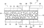
- FIG. 1 is a diagram conceptually showing an example of the piezoelectric element of the present invention.
- FIG. 2 is a schematic plan view of the piezoelectric element shown in FIG.
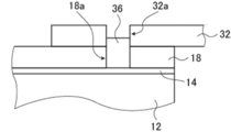
- FIG. 3 is a partially enlarged view conceptually showing another example of the piezoelectric element of the present invention.
- FIG. 4 is a partially enlarged view conceptually showing another example of the piezoelectric element of the present invention.
- FIG. 5 is a partially enlarged view conceptually showing another example of the piezoelectric element of the present invention.
- FIG. 6 is a partially enlarged view conceptually showing another example of the piezoelectric element of the present invention.
- FIG. 7 is a partially enlarged view conceptually showing another example of the piezoelectric element of the present invention.
- FIG. 1 is a diagram conceptually showing an example of the piezoelectric element of the present invention.
- FIG. 2 is a schematic plan view of the piezoelectric element shown in FIG.
- FIG. 3 is a partially enlarged view conceptually showing
- FIG. 8 is a partially enlarged view conceptually showing another example of the piezoelectric element of the present invention.
- FIG. 9 is a partially enlarged view conceptually showing another example of the piezoelectric element of the present invention.
- FIG. 10 is a conceptual diagram for explaining a method for manufacturing the piezoelectric element shown in FIG.
- FIG. 11 is a conceptual diagram for explaining a method for manufacturing the piezoelectric element shown in FIG.
- FIG. 12 is a conceptual diagram for explaining a method for manufacturing the piezoelectric element shown in FIG.
- FIG. 13 is a conceptual diagram for explaining a method for manufacturing the piezoelectric element shown in FIG.
- FIG. 14 is a conceptual diagram for explaining a method for manufacturing the piezoelectric element shown in FIG. FIG.
- FIG. 15 is a conceptual diagram for explaining a method for manufacturing the piezoelectric element shown in FIG.
- FIG. 16 is a conceptual diagram for explaining a method for manufacturing the piezoelectric element shown in FIG.
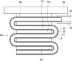
- FIG. 17 is a diagram conceptually showing another example of the piezoelectric element of the present invention.
- FIG. 18 is a diagram conceptually showing an example of a speaker using the piezoelectric element shown in FIG.
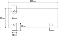
- FIG. 19 is a conceptual diagram for explaining a method of measuring electrical resistance in an embodiment.
- the description of the constituent elements described below may be based on the representative embodiments of the present invention, but the present invention is not limited to such embodiments.
- the numerical range represented by using "-" means a range including the numerical values before and after "-" as the lower limit value and the upper limit value.
- the figures shown below are conceptual diagrams for explaining the present invention, and are the thickness of each layer, the size of the through hole, the positional relationship of each member (site), and each member. The size of the product is different from the actual product.
- FIG. 1 and 2 show conceptually an example of the piezoelectric element of the present invention.
- FIG. 1 is a diagram conceptually showing a cross section of a piezoelectric element cut in the thickness direction
- FIG. 2 is a plan view of the piezoelectric element shown in FIG. 1.
- the thickness direction of the piezoelectric element is the stacking direction of the piezoelectric layer, the electrode layer, and the protective layer in the piezoelectric film described later.
- the plan view is a view of the piezoelectric element of the present invention as viewed from the thickness direction.
- the piezoelectric element 10 has a piezoelectric film 30, a first lead wire 32, a second lead wire 34, a first filling member 36, and a second filling member 38.
- the first lead wire 32 and the second lead wire 34 are conductive members in the present invention.
- the piezoelectric film 30 includes a piezoelectric layer 12, a first electrode layer 14 laminated on one surface of the piezoelectric layer 12, and a first protective layer 18 laminated on the surface of the first electrode layer 14. It has a second electrode layer 16 laminated on the other surface of the piezoelectric layer 12, and a second protective layer 20 laminated on the surface of the second electrode layer 16.
- the first lead wire 32 is provided so as to be laminated on the first protective layer 18 of the piezoelectric film 30.
- a through hole 18a is formed in the first protective layer 18, and a through hole 32a is formed in the first lead wire 32.
- the through hole 18a and the through hole 32a have a cylindrical shape having the same diameter and coincide with the center in the plane direction.
- the first filling member 36 is filled in both through holes so as to fill the through holes 18a and the through holes 32a, that is, to completely fill the through holes.
- the second lead wire 34 is provided so as to be laminated on the second protective layer 20 of the piezoelectric film 30.
- a through hole 20a is formed in the second protective layer 20, and a through hole 34a is formed in the second lead wire 34.
- the through hole 20a and the through hole 34a have a cylindrical shape having the same diameter and coincide with the center in the plane direction.
- the second filling member 38 is filled in both through holes so as to fill the through holes 20a and the through holes 34a, that is, to completely fill the through holes 20a.
- the plane direction is the plane direction of the main surface of the piezoelectric film 30.
- the main surface is the maximum surface of a sheet-like material (film, plate-like material, layer), and is both sides in the thickness direction.
- the piezoelectric layer 12 of the piezoelectric film 30 contains the piezoelectric particles 26, which are piezoelectric particles, in the matrix 24 containing the polymer material. That is, the piezoelectric layer 12 is a polymer composite piezoelectric body.
- the polymer composite piezoelectric body (piezoelectric layer 12) is used, for example, in an electroacoustic conversion film.
- the polymer composite piezoelectric material used in the electroacoustic conversion film preferably meets the following requirements.
- the normal temperature is 0 to 50 ° C.
- the speaker vibrates the piezoelectric particles at a frequency in the audio band of 20 Hz to 20 kHz, and the vibration energy causes the entire diaphragm (polymer composite piezoelectric material) to vibrate as a unit, and the sound is reproduced.
- the polymer composite piezoelectric body is required to have an appropriate hardness.
- the frequency characteristic of the speaker is smooth, the amount of change in sound quality when the minimum resonance frequency f 0 changes with the change in curvature also becomes small. Therefore, it is required that the loss tangent of the polymer composite piezoelectric body is moderately large.
- the minimum resonance frequency f 0 of the diaphragm for a speaker is given by the following equation.
- s is the stiffness of the vibration system
- m is the mass.
- the flexible polymer composite piezoelectric material used as an electroacoustic conversion film is required to behave hard against vibrations of 20 Hz to 20 kHz and soft against vibrations of several Hz or less. Further, the loss tangent of the polymer composite piezoelectric body is required to be appropriately large for vibrations of all frequencies of 20 kHz or less.
- a high molecular weight solid has a viscoelastic relaxation mechanism, and a large-scale molecular motion with a rise in temperature or a decrease in frequency causes a decrease in storage elastic modulus (Young's modulus) (relaxation) or a maximum loss elastic modulus (absorption). Observed as. Among them, the relaxation caused by the microBrownian motion of the molecular chain in the amorphous region is called main dispersion, and a very large relaxation phenomenon is observed. The temperature at which this main dispersion occurs is the glass transition point (Tg), and the viscoelastic relaxation mechanism appears most prominently.
- Tg glass transition point
- the polymer composite piezoelectric body (piezoelectric layer 12), by using a polymer material whose glass transition point is at room temperature for the matrix, it is hard against vibrations of 20 Hz to 20 kHz and against slow vibrations of several Hz or less. Realizes a polymer composite piezoelectric that behaves softly. In particular, from the viewpoint that this behavior is preferably exhibited, it is preferable to use a polymer material having a glass transition point at a frequency of 1 Hz at room temperature, that is, 0 to 50 ° C., for the matrix of the polymer composite piezoelectric material.
- the polymer material having a glass transition point at room temperature is, in other words, a polymer material having viscoelasticity at room temperature.
- the polymer material having viscoelasticity at room temperature various known materials can be used. It is preferable to use a polymer material having a maximum value of tangent Tan ⁇ of 0.5 or more at a frequency of 1 Hz by a dynamic viscoelasticity test at room temperature, that is, 0 to 50 ° C. As a result, when the polymer composite piezoelectric body is slowly bent by an external force, the stress concentration at the interface between the polymer matrix and the piezoelectric particles at the maximum bending moment portion is relaxed, and high flexibility can be expected.
- the polymer material having viscoelasticity at room temperature preferably has a storage elastic modulus (E') at a frequency of 1 Hz as measured by dynamic viscoelasticity measurement of 100 MPa or more at 0 ° C. and 10 MPa or less at 50 ° C.
- E' storage elastic modulus
- the polymer material having viscoelasticity at room temperature has a relative permittivity of 10 or more at 25 ° C.
- a voltage is applied to the polymer composite piezoelectric body, a higher electric field is applied to the piezoelectric particles in the polymer matrix, so that a large amount of deformation can be expected.
- the polymer material has a relative permittivity of 10 or less at 25 ° C.
- polymer material having viscoelasticity at room temperature satisfying such conditions examples include cyanoethylated polyvinyl alcohol (cyanoethylated PVA), polyvinyl acetate, polyvinylidene chloride core acrylonitrile, polystyrene-vinyl polyisoprene block copolymer, and polyvinylmethyl. Examples thereof include ketones and polybutylmethacrylate. Further, as these polymer materials, commercially available products such as Hybler 5127 (manufactured by Kuraray Co., Ltd.) can also be suitably used.
- Hybler 5127 manufactured by Kuraray Co., Ltd.
- the polymer material it is preferable to use a material having a cyanoethyl group, and it is particularly preferable to use cyanoethylated PVA.
- the matrix 24 only one kind of these polymer materials may be used, or a plurality of kinds may be used in combination (mixed).
- a plurality of polymer materials may be used in combination, if necessary. That is, in the matrix 24, in addition to a polymer material having viscoelasticity at room temperature such as cyanoethylated PVA for the purpose of adjusting dielectric properties and mechanical properties, other dielectric polymer materials are added as needed. It may be added.
- dielectric polymer material examples include polyvinylidene fluoride, vinylidene fluoride-tetrafluoroethylene copolymer, vinylidene fluoride-trifluoroethylene copolymer, and vinylidene fluoride-trifluoroethylene copolymer.
- fluoropolymers such as polyvinylidene fluoride-tetrafluoroethylene copolymer, vinylidene cyanide-vinyl acetate copolymer, cyanoethyl cellulose, cyanoethyl hydroxysaccharose, cyanoethyl hydroxycellulose, cyanoethyl hydroxypurrane, cyanoethyl methacrylate, cyanoethyl acrylate, cyanoethyl.
- Cyano groups such as hydroxyethyl cellulose, cyanoethyl amylose, cyanoethyl hydroxypropyl cellulose, cyanoethyl dihydroxypropyl cellulose, cyanoethyl hydroxypropyl amylose, cyanoethyl polyacrylamide, cyanoethyl polyacrylate, cyanoethyl pullulan, cyanoethyl polyhydroxymethylene, cyanoethyl glycidol pullulan, cyanoethyl saccharose and cyanoethyl sorbitol.
- polymers having a cyanoethyl group synthetic rubbers such as nitrile rubber and chloroprene rubber, and the like are exemplified. Among them, a polymer material having a cyanoethyl group is preferably used. Further, in the matrix 24 of the piezoelectric layer 12, the dielectric polymer added in addition to the material having viscoelasticity at room temperature such as cyanoethylated PVA is not limited to one type, and a plurality of types may be added. ..
- the matrix 24 contains vinyl chloride resin, polyethylene, polystyrene, methacrylic resin, thermoplastic resin such as polybutene and isobutylene, and phenol resin for the purpose of adjusting the glass transition point Tg.
- Urea resin, melamine resin, alkyd resin, mica and other thermosetting resins may be added.
- a tackifier such as rosin ester, rosin, terpene, terpene phenol, and petroleum resin may be added.
- the amount to be added when a material other than the polymer material having viscoelasticity at room temperature such as cyanoethylated PVA is added is not particularly limited, but is 30 mass in proportion to the matrix 24. It is preferably% or less.
- the characteristics of the polymer material to be added can be exhibited without impairing the viscoelastic relaxation mechanism in the matrix 24, so that the dielectric constant can be increased, the heat resistance can be improved, and the adhesion to the piezoelectric particles 26 and the electrode layer can be improved. In this respect, favorable results can be obtained.
- the piezoelectric layer 12 includes the piezoelectric particles 26 in such a matrix 24.
- the piezoelectric particles 26 are preferably made of ceramic particles having a perovskite-type or wurtzite-type crystal structure.
- the ceramic particles constituting the piezoelectric particles 26 include lead zirconate titanate (PZT), lanthanum lead zirconate titanate (PLZT), barium titanate (BaTIO 3 ), zinc oxide (ZnO), and titanium.
- PZT lead zirconate titanate
- PLA 3 lanthanum lead zirconate titanate
- ZnO zinc oxide
- titanium examples thereof include a solid solution (BFBT) of barium acid acid and bismuth ferrite (BiFe 3).
- the particle size of the piezoelectric particles 26 is not limited, and may be appropriately selected depending on the size of the piezoelectric layer 12 (piezoelectric film 30), the application of the piezoelectric element 10, and the like.
- the particle size of the piezoelectric particles 26 is preferably 1 to 10 ⁇ m. By setting the particle size of the piezoelectric particles 26 in this range, favorable results can be obtained in that the piezoelectric film 30 can achieve both high piezoelectric characteristics and flexibility.
- the piezoelectric particles 26 in the piezoelectric layer 12 are irregularly dispersed in the matrix 24, but the present invention is not limited to this. That is, the piezoelectric particles 26 in the piezoelectric layer 12 may be irregularly dispersed or regularly dispersed in the matrix 24 as long as they are preferably uniformly dispersed. Further, the piezoelectric particles 26 may or may not have the same particle size.
- the amount ratio of the matrix 24 to the piezoelectric particles 26 in the piezoelectric layer 12 is not limited, and the size and thickness of the piezoelectric film 30 in the plane direction, the use of the piezoelectric element 10, and the use of the piezoelectric element 10 are not limited. It may be appropriately set according to the characteristics required for the piezoelectric film 30 and the like.
- the volume fraction of the piezoelectric particles 26 in the piezoelectric layer 12 is preferably 30 to 80%, more preferably 50% or more. Therefore, the volume fraction of the piezoelectric particles 26 in the piezoelectric layer 12 is more preferably 50 to 80%.
- the thickness of the piezoelectric layer 12 is not particularly limited, and may be appropriately set according to the application of the piezoelectric element 10, the characteristics required for the piezoelectric element 10, and the like.
- the thickness of the piezoelectric layer 12 is preferably 8 to 300 ⁇ m, more preferably 8 to 200 ⁇ m, still more preferably 10 to 150 ⁇ m, and particularly preferably 15 to 100 ⁇ m.
- the piezoelectric layer 12 is preferably polarized (polled) in the thickness direction.
- the polarization treatment will be described in detail later.
- the piezoelectric layer 12 is not limited to the polymer composite piezoelectric body as shown in the illustrated example, and a known piezoelectric material can be used.
- Examples of the piezoelectric material that can be used for the piezoelectric element of the present invention include polyvinylidene fluoride, a fluororesin other than polyvinylidene fluoride, and a laminated film of a film made of poly L lactic acid and a film made of poly D lactic acid. Illustrated.
- a polymer composite piezoelectric body in which the piezoelectric particles 26 are dispersed in a matrix 24 containing a polymer material as shown in the illustrated example is available. It is suitably used as the piezoelectric layer 12.
- the piezoelectric film 30 has a first electrode layer 14 on one surface of such a piezoelectric layer 12 and a first protective layer 18 on the surface thereof. .. Further, the piezoelectric film 30 has a structure in which the second electrode layer 16 is provided on the surface of the piezoelectric layer 12 opposite to the first electrode layer 14, and the second protective layer 20 is provided on the surface thereof. .. In other words, the first protective layer 18 is provided on the surface of the first electrode layer 14 opposite to the piezoelectric layer 12. Further, the second protective layer 20 is provided on the surface of the second electrode layer 16 opposite to the piezoelectric layer 12.
- the first electrode layer 14 and the second electrode layer 16 form an electrode pair. That is, the piezoelectric film 30 sandwiches both sides of the piezoelectric layer 12 between electrode pairs, that is, the first electrode layer 14 and the second electrode layer 16, and the laminated body is combined with the first protective layer 18 and the second protective layer 20. It has a structure sandwiched between. In such a piezoelectric film 30, the region held by the first electrode layer 14 and the second electrode layer 16 is expanded and contracted according to the applied voltage.
- the first and second electrodes in the first electrode layer 14 and the first protective layer 18, and the second electrode layer 16 and the second protective layer 20 are for convenience in order to explain the piezoelectric element 10. It is attached to the target. Therefore, the first and second members of the piezoelectric element 10 have no technical meaning and are irrelevant to the actual usage state such as the position in the vertical direction. The same applies to the lead wire and the filling member described later in this respect.
- the first protective layer 18 and the second protective layer 20 cover the first electrode layer 14 and the second electrode layer 16, and the piezoelectric layer 12 is appropriately rigid and mechanical. It plays the role of imparting strength. That is, in the piezoelectric film 30, the piezoelectric layer 12 composed of the matrix 24 and the piezoelectric particles 26 exhibits extremely excellent flexibility against slow bending deformation, but is rigid depending on the application. And mechanical strength may be insufficient.
- the piezoelectric element 10 is provided with a first protective layer 18 and a second protective layer 20 to supplement the piezoelectric element 10.
- the first protective layer 18 and the second protective layer 20 are not limited, and various sheet-like materials can be used, and as an example, various resin films are preferably exemplified.
- various resin films are preferably exemplified.
- PET polyethylene terephthalate
- PP polypropylene
- PS polystyrene
- PC polycarbonate
- PPS polyphenylene sulfide
- PMMA polymethylmethacrylate
- PEI Polyetherimide
- PEI polyimide
- PI polyimide
- PEN polyethylene naphthalate
- TAC triacetyl cellulose
- a resin film made of a cyclic olefin resin or the like are preferably used.
- the thickness of the first protective layer 18 and the second protective layer 20 there is no limitation on the thickness of the first protective layer 18 and the second protective layer 20. Further, the thicknesses of the first protective layer 18 and the second protective layer 20 are basically the same, but may be different. Here, if the rigidity of the first protective layer 18 and the second protective layer 20 is too high, not only the expansion and contraction of the piezoelectric layer 12 is restrained, but also the flexibility is impaired. Therefore, the thinner the first protective layer 18 and the second protective layer 20, the more advantageous it is, except when mechanical strength and good handleability as a sheet-like material are required.
- the thickness of the first protective layer 18 and the second protective layer 20 is twice or less the thickness of the piezoelectric layer 12, the rigidity can be ensured and the appropriate flexibility can be achieved. Preferred results can be obtained in terms of points.
- the thickness of the first protective layer 18 and the second protective layer 20 is preferably 100 ⁇ m or less. 50 ⁇ m or less is more preferable, and 25 ⁇ m or less is further preferable.
- the first electrode layer 14 is between the piezoelectric layer 12 and the first protective layer 18, and the second electrode layer is between the piezoelectric layer 12 and the second protective layer 20. 16 are provided respectively.
- the first electrode layer 14 and the second electrode layer 16 are provided for applying a voltage to the piezoelectric layer 12.
- the materials for forming the first electrode layer 14 and the second electrode layer 16 are not limited, and various conductors can be used. Specifically, metals such as carbon, palladium, iron, tin, aluminum, nickel, platinum, gold, silver, copper, titanium, chromium and molybdenum, alloys thereof, laminates and composites of these metals and alloys, In addition, indium tin oxide and the like are exemplified. Among them, copper, aluminum, gold, silver, platinum, and indium tin oxide are preferably exemplified as the first electrode layer 14 and the second electrode layer 16.
- the method of forming the first electrode layer 14 and the second electrode layer 16 and the film formation by a vapor deposition method such as vacuum vapor deposition and sputtering, the film formation by plating, and the above-mentioned
- a vapor deposition method vacuum film deposition method
- sputtering the film formation by plating
- Various known methods such as a method of attaching a foil formed of the above material can be used.
- thin films such as copper and aluminum formed by vacuum deposition are suitably used as the first electrode layer 14 and the second electrode layer 16 because the flexibility of the piezoelectric element 10 can be ensured.
- Ru a copper thin film produced by vacuum vapor deposition is particularly preferably used.
- the thickness of the first electrode layer 14 and the second electrode layer 16 There is no limitation on the thickness of the first electrode layer 14 and the second electrode layer 16. Further, the thicknesses of the first electrode layer 14 and the second electrode layer 16 are basically the same, but may be different.
- the rigidity of the first electrode layer 14 and the second electrode layer 16 is too high, not only the expansion and contraction of the piezoelectric layer 12 is restrained, but also the expansion and contraction of the piezoelectric layer 12 is restrained. Flexibility is also impaired. Therefore, the thinner the first electrode layer 14 and the second electrode layer 16 are, the more advantageous they are, as long as the electrical resistance does not become too high.
- the product of the thickness of the first electrode layer 14 and the second electrode layer 16 and Young's modulus is the thickness of the first protective layer 18 and the second protective layer 20 and Young's modulus. If it is less than the product of, it is preferable because the flexibility is not significantly impaired.
- the Young's modulus of PET is about 6.2 GPa, which is copper. Young's modulus is about 130 GPa.
- the thickness of the first protective layer 18 and the second protective layer 20 is 25 ⁇ m
- the thickness of the first electrode layer 14 and the second electrode layer 16 is preferably 1.2 ⁇ m or less. , 0.3 ⁇ m or less is more preferable, and 0.1 ⁇ m or less is further preferable.
- the piezoelectric film 30 sandwiches the piezoelectric layer 12 having the piezoelectric particles 26 in the matrix 24 containing the polymer material having viscoelasticity at room temperature between the first electrode layer 14 and the second electrode layer 16. Further, the laminated body has a structure in which the first protective layer 18 and the second protective layer 20 are sandwiched. In such a piezoelectric film 30, it is preferable that the maximum value of the loss tangent (Tan ⁇ ) at a frequency of 1 Hz by dynamic viscoelasticity measurement exists at room temperature, and the maximum value of 0.1 or more exists at room temperature. More preferred.
- the piezoelectric film 30 is subjected to a relatively slow and large bending deformation of several Hz or less from the outside, the strain energy can be effectively diffused to the outside as heat, so that the polymer matrix and the piezoelectric particles can be used. It is possible to prevent cracks from occurring at the interface of.
- the piezoelectric film 30 preferably has a storage elastic modulus (E') at a frequency of 1 Hz as measured by dynamic viscoelasticity measurement of 10 to 30 GPa at 0 ° C. and 1 to 10 GPa at 50 ° C.
- E' storage elastic modulus
- the piezoelectric film 30 can have a large frequency dispersion in the storage elastic modulus (E') at room temperature. That is, it can behave hard for vibrations of 20 Hz to 20 kHz and soft for vibrations of several Hz or less.
- the product of the thickness and the storage elastic modulus (E') at a frequency of 1 Hz measured by dynamic viscoelasticity is 1.0 ⁇ 10 6 to 2.0 ⁇ 10 6 N / m at 0 ° C. , It is preferably 1.0 ⁇ 10 5 to 1.0 ⁇ 10 6 N / m at 50 ° C.
- the piezoelectric film 30 can be provided with appropriate rigidity and mechanical strength as long as the flexibility and acoustic characteristics are not impaired.
- the piezoelectric film 30 preferably has a loss tangent (Tan ⁇ ) of 0.05 or more at 25 ° C. and a frequency of 1 kHz in the master curve obtained from the dynamic viscoelasticity measurement.
- Ton ⁇ loss tangent
- the frequency characteristics of the speaker using the piezoelectric film 30 become smooth, and the amount of change in sound quality when the minimum resonance frequency f0 changes with the change in the curvature of the speaker can be reduced.
- the piezoelectric film 30 constituting the piezoelectric element 10 of the present invention has, for example, a sticking layer for adhering the electrode layer and the piezoelectric layer 12, and an electrode layer and a protective layer. It may have a sticking layer for sticking and.
- the adhesive may be an adhesive or an adhesive.
- a polymer material from which the piezoelectric particles 26 are removed from the piezoelectric layer 12, that is, the same material as the matrix 24 can also be preferably used.
- the bonding layer may be provided on both the first electrode layer 14 side and the second electrode layer 16 side, or may be provided only on one of the first electrode layer 14 side and the second electrode layer 16 side. good.
- the piezoelectric element of the present invention is in contact with a protective layer in order to drive the piezoelectric film 30, and is conductive such as a lead wire for electrically connecting the electrode layer of the piezoelectric film 30 and an external device such as a drive power supply. It has a sex member.
- the conductive member is electrically connected to the electrode layer by the conductive filling member filled in the through hole formed in the protective layer of the piezoelectric film 30.
- the conductive member also has a through hole. At least a part of the through hole of the conductive member overlaps with the through hole of the protective layer in the surface direction, and at least a part of the filling material comes into contact with the inner wall surface.
- the piezoelectric element 10 of the illustrated example has a first lead wire 32 laminated on the first protective layer 18 and a second lead wire 34 laminated on the second protective layer 20 as a conductive member.
- the first lead wire 32 and the second lead wire 34 are plate-shaped as an example.
- a through hole 18a is formed in the first protective layer 18, and a through hole 32a is formed in the first lead wire 32.
- the through hole 18a and the through hole 32a are cylindrical with the same diameter, and preferably, the centers of the upper and lower surfaces coincide with each other in the surface direction.
- a through hole 20a is formed in the second protective layer 20, and a through hole 34a is formed in the second lead wire 34.
- the through hole 20a and the through hole 34a are cylindrical with the same diameter, and preferably, the centers of the upper and lower surfaces coincide with each other in the surface direction.
- the through hole 18a of the first protective layer 18 is filled with the first filling member 36. At least a part of the first filling member 36 comes into contact with the inner wall surface of the through hole 32a of the first lead wire 32. As a result, the first lead wire 32 and the first electrode layer 14 are connected.
- the first filling member 36 fills not only the through hole 18a of the second protective layer 20 but also the through hole 32a of the first lead wire 32, that is, completely fills the through hole 32a. It is filled.
- the through hole 20a of the second protective layer 20 is filled with the second filling member 38.
- the second filling member 38 comes into contact with the inner wall surface of the through hole 34a of the second lead wire 34. As a result, the second lead wire 34 and the second electrode layer 16 are connected.
- the second filling member 38 fills not only the through hole 20a of the second protective layer 20 but also the through hole 34a of the second lead wire 34, that is, completely fills the through hole 34a. It is filled.
- the piezoelectric element of the present invention reduces the resistance of connection between the conductive member and the electrode layer for connecting to an external device in the piezoelectric element using the piezoelectric film as described above. Moreover, the productivity of the connection between the electrode layer and the conductive member is improved.
- a piezoelectric film in which electrode layers are provided on both sides of a piezoelectric layer and a protective layer is provided so as to cover the electrode layers is known.
- a lead wire or the like for connecting an external device such as a drive power supply to the electrode layer to the electrode layer.
- Various methods can be considered for connecting the electrode layer and the lead wire.
- the connection portion between the electrode layer and the lead wire also has flexibility.
- connection method As a connection method that satisfies such a requirement, a through hole is provided in the protective layer, the through hole is filled with a conductive filling member such as a conductive paste, and a lead wire is provided so as to cover the through hole (filling member).
- a conductive filling member such as a conductive paste
- a lead wire is provided so as to cover the through hole (filling member).
- the resistance of the connection between the electrode layer and the lead wire is low and that the connection between the electrode layer and the lead wire can be performed with high productivity.
- a through hole is provided in the protective layer to fill the conductive paste or the like and a lead wire is provided so as to cover the through hole, the contact area between the filling member and the lead wire cannot be increased, and the electrode layer and the lead cannot be increased.
- the connection with the wire cannot be made low resistance.
- a resin film is preferably used as the protective layer of the piezoelectric film.
- the conductive paste to be the filling member a type that is cured by heating / sintering cannot be used, and a type that is cured by volatilization of the solvent is used. Therefore, in a configuration in which a through hole is provided in the protective layer to fill the conductive paste or the like and a lead wire is provided so as to cover the through hole, it takes time for the solvent to volatilize and cure the conductive paste, and the productivity is low. ..
- a through hole is also provided in the lead wire (conductive member), and the through hole of the protective layer and the through hole of the lead wire are overlapped at least partially in the surface direction. At least a part of the conductive paste (filling member) is brought into contact with the inner wall of the through hole of the lead wire.
- the through hole of the protective layer and the through hole of the lead wire are completely overlapped in the plane direction, or one of them contains the other and leads as described later.
- the through holes of the wire are also filled with the conductive paste, i.e., completely filled.
- the contact area between the filling member and the lead wire can be increased as compared with the above-mentioned method, and as a result, the resistance of the connection between the electrode layer and the lead wire can be reduced.
- the lead wire also has a through hole, and at least a part of the lead wire overlaps with the through hole of the protective layer in the plane direction, so that the conductive paste filled in the through hole is opened to the atmosphere. As a result, the time required for solvent volatilization and curing of the conductive paste can be significantly shortened, and the connection between the electrode layer and the lead wire can be performed with high productivity.
- the first and second in the electrode layer, the protective layer, the lead wire and the filling member have no technical meaning.
- the structure of the connection between the first electrode layer 14 and the first lead wire 32 and the structure of the connection between the second electrode layer 16 and the second lead wire 34 are basically the same. Therefore, in the following description, when it is not necessary to distinguish between the first electrode layer 14 side and the second electrode layer 16 side, the first electrode layer 14 side is used as a representative example.
- the first protective layer 18 (second protective layer 20) has a through hole 18a (through hole 20a) in the first lead wire 32 (second lead wire 34).
- a through hole 32a (through hole 34a) is formed in each. Both through holes partially overlap in the plane direction.
- both through holes are cylindrical with the same diameter and are centered in the plane direction.
- the through hole 18a is filled with the first filling member 36 (second filling member 38).
- the first lead wire 32 and the first electrode layer 14 are connected by contacting at least a part of the first filling member 36 with the inner wall surface of the through hole 32a of the first lead wire 32.
- the first filling member 36 is filled so as to fill not only the through hole 18a of the first protective layer 18 but also the through hole 32a of the first lead wire 32, that is, completely fill it. Will be done.
- the conductive paste that becomes the first filling member 36 (second filling member) filled in the through hole 18a of the first protective layer 18 is opened to the atmosphere by the through hole 32a of the first lead wire 32.
- the time required for solvent volatilization and curing of the conductive paste can be significantly shortened, and the connection between the electrode layer and the lead wire can be performed with high productivity.
- the curing of the conductive paste can be further promoted and the productivity can be improved.
- the contact area between the first filling member 36 and the first lead wire 32 is also sufficient. It is possible to secure and reduce the resistance of the connection between the first electrode layer 14 and the first lead wire.
- the through hole 18a of the first protective layer 18 and the through hole 32a of the first lead wire 32 are cylindrical with the same diameter, and their centers are aligned in the plane direction. That is, the through hole 18a and the through hole 32a completely overlap (match) in the plane direction.
- the piezoelectric element 10 of the present invention is not limited to this, and various configurations can be used.
- a configuration in which the through hole 18a of the first protective layer 18 has a larger diameter than the through hole 32a of the first lead wire 32 is exemplified.
- a configuration in which the through hole 32a of the first lead wire 32 has a larger diameter than the through hole 18a of the first protective layer 18 is cylindrical. Will be done.
- the center of the through hole 18a of the first protective layer 18 and the through hole 32a of the first lead wire 32 coincide with each other.
- the configuration of the through hole 18a and the through hole 32a in which one contains the other in the plane direction is not limited to this, and if one contains the other, the through hole 18a and the through hole 32a are included.
- the center may be different.
- the through hole 18a of the first protective layer 18 and the through hole 32a of the first lead wire 32 coincide with each other in the surface direction, or one through hole makes the other through hole in the surface direction.
- the present invention is not limited thereto.
- the piezoelectric element of the present invention is conceptualized in FIG. 5 regardless of whether the diameters of the through hole 18a and the through hole 32a are the same or the diameters of the through hole 18a and the through hole 32a are different.
- the through hole 18a and the through hole 32a may be displaced in the plane direction. That is, the overlap of the through hole 18a and the through hole 32a in the surface direction may be a part.
- the curing time of the conductive paste to be the first filling member 36 can be shortened to improve the productivity, and the amount of the conductive paste used can be reduced to reduce the cost. It is preferable that the through hole 18a and the through hole 32a completely overlap in the surface direction, including the configuration in which the through hole is included in the other through hole.
- the through hole 18a of the first protective layer 18 and the through hole 32a of the first lead wire 32 are both cylindrical (cylindrical), but the present invention is not limited thereto.
- the through hole 18a and / or the through hole 32a may be a prism such as a triangular prism and a quadrangular prism, or may be an elliptical prism. That is, if the through hole 18a penetrates the first protective layer 18 in the thickness direction, and if the through hole 32a penetrates the first lead wire 32 in the thickness direction, the shape is not limited. ..
- the through hole 18a and the through hole 32a are preferably cylindrical in terms of ease of processing, ease of filling the conductive paste to be the first filling member 36, and the like.
- the through hole 18a and / or the through hole 32a may have a shape in which the size in the plane direction gradually changes in the thickness direction.
- the through hole 18a and / or the through hole 32a may have a truncated cone shape, an elliptical cone trapped shape, a prismatic cone shape, or the like that gradually reduces or expands the diameter toward the piezoelectric layer 12. ..
- the shape of the through hole is preferably a truncated cone shape.
- the size of the through hole 18a of the first protective layer 18 and the through hole 32a of the first lead wire 32 for example, the diameter of the cylinder in the illustrated example. That is, the size of the through hole 18a and the through hole 32a is appropriately set to a size that can secure sufficient conductivity according to the size of the piezoelectric film 30, the width of the band of the first lead wire 32, and the like. do it. Further, as shown in FIGS. 3 and 4, when the sizes of the through hole 18a and the through hole 32a are different, there is no limitation on the difference.
- the size of the through hole 18a and the through hole 32a is such that at least a part of the first filling member 36 filled in the through hole 18a is surely in contact with the inner wall surface of the through hole 32a. It is necessary to appropriately consider the difference between the above, the filling amount of the conductive paste or the like in the through hole 18a or the through hole 32a, the filling method of the conductive paste or the like in the through hole 18a or the through hole 32a, and the like. ..
- a plurality of through holes 18a of the first protective layer 18 and / or a plurality of through holes 32a of the first lead wire 32 may be provided.
- the number of through holes 18a and through holes 32a is not limited, and is appropriately determined according to the size of the piezoelectric film 30, the size of the first lead wire 32, the conductivity required for connection, and the like. Just set it. Further, the number of through holes 18a and the number of through holes 32a may be the same or different. For example, the number of through holes 18a may be one and the number of through holes 32a may be two or more.
- one through hole 18a and one through hole 32a may overlap (include) one through hole.
- the 18a and the plurality of through holes 32a may overlap, the plurality of through holes 18a and one through hole 32a may overlap, or the plurality of through holes may overlap each other.
- the through holes partially overlapping in the surface direction and the through holes completely overlapping (encapsulating) in the surface direction are provided. It may be mixed.
- the first filling member 36 is filled so as to fill not only the through hole 18a of the first protective layer 18 but also the through hole 32a of the first lead wire 32.
- the piezoelectric element of the present invention is not limited to this, and the first filling member 36 may be at least partially filled in the through hole 32a and may come into contact with the inner wall surface of the through hole 32a.
- the first filling member 36 may be configured to fill the through hole 18a and reach halfway in the thickness direction of the through hole 32a.
- the contact area between the first filling member 36 and the first lead wire 32 can be increased to reduce the resistance of the connection between the first electrode layer 14 and the first lead wire 32.
- the first filling member 36 also fills the through hole 32a of the first lead wire 32 in addition to the through hole 18a of the first protective layer 18 so as to further overflow.
- the first lead wire 32 may come into contact with the main surface opposite to the first protective layer 18.
- the first filling member 36 may exist between the first protective layer 18 and the first lead wire 32, as conceptually shown in FIG. That is, the first filling member 36 may come into contact with the main surface of the first lead wire 32 on the first protective layer 18 side.
- a piezoelectric element having this configuration can be manufactured. Similar to the configuration shown in FIG. 7, by having such a configuration, the contact area between the first filling member 36 and the first lead wire 32 is increased, and the first electrode layer 14 and the first lead wire 32 are connected to each other. The resistance of the connection can be made smaller.
- the configuration shown in FIG. 7 and the configuration shown in FIG. 8 may be used in combination.
- the first filling member 36 (second filling member 38) is not limited, and various known conductive materials can be used as long as the through holes can be filled.
- the first filling member 36 is formed by using a conductive paste which has a conductive filler, a binder (resin), a solvent and the like and is cured by volatilization of the solvent as a preferable example.
- a conductive paste which has a conductive filler, a binder (resin), a solvent and the like and is cured by volatilization of the solvent.
- the conductive paste used in the present invention various known pastes can be used as long as they have a conductive filler, a binder and a solvent and are cured by the volatilization of the solvent.
- silver paste, copper paste, nickel paste, carbon paste, gold paste and the like are exemplified.
- commercially available products such as the Dotite series manufactured by Fujikura Kasei Co., Ltd. can also be suitably used.
- the first lead wire 32 (second lead wire 34) is also not limited, and various known lead wires (lead wires) used for electrical connection between the two points can be used.
- lead wires include copper foil, lead wires having a conductive plating such as nickel on the surface of the copper foil, and copper or the like on a film-like substrate such as an FPC (Flexible Printed Circuits) substrate. Examples thereof include those in which the conductor is patterned and exposed.
- the first lead wire 32 is not limited to a plate shape (strip shape), and may be a rod shape or the like as long as it can form a through hole 32a.
- the conductive member for connecting the electrode layer of the piezoelectric film and the external device is not limited to the lead wire, and the electrode layer and the external device are electrically connected. If possible, various types are available.
- the conductive member other than the lead wire an FPC substrate or the like is exemplified.
- the through hole provided in the conductive member needs to include at least a part of the conductive portion of the conductive member such as wiring.
- the conductive member, including the first lead wire 32 is preferably flexible regardless of the material and form.
- the surface roughness Ra (arithmetic mean roughness Ra) of the surface of the first lead wire 32 (second lead wire 34 (conductive member)) in contact with the first protective layer 18 is 0. It is preferably 8.8 ⁇ m or more.
- the surface roughness Ra does not have to be the entire surface of the contact surface of the first lead wire 32 with the first protective layer 18. That is, the first lead wire 32 may have a surface roughness Ra of at least the contact portion with the first filling member 36 of 0.8 ⁇ m or more on the contact surface with the first protective layer 18.
- the first filling member 36 also exists between the first protective layer 18 and the first lead wire 32.
- the surface roughness Ra of the surface of the first lead wire 32 in contact with the first protective layer 18 is 0.8 ⁇ m or more
- the contact area between the first filling member 36 and the first lead wire 32 is determined. Can be bigger.
- the resistance of the connection between the first electrode layer 14 and the first lead wire 32 can be made smaller.
- the through hole 18a of the first protective layer 18 is larger than the through hole of the first lead wire 32, the surface of the first lead wire 32 that comes into contact with the first protective layer 18.
- the contact area between the first filling member 36 and the first lead wire 32 can be made larger. As a result, the resistance of the connection between the first electrode layer 14 and the first lead wire 32 can be made smaller.
- the surface roughness Ra of the surface of the first lead wire 32 in contact with the first protective layer 18 is more preferably 1.0 ⁇ m or more.
- the upper limit of the surface roughness Ra of the surface of the first lead wire 32 in contact with the first protective layer 18 is not limited, but is preferably 100 ⁇ m or less.
- the roughening treatment may be performed by a known method.
- Examples of the method for roughening the first lead wire 32 include sandblasting and etching.
- the surface roughness Ra of the surface of the first lead wire 32 in contact with the first protective layer 18 may be measured by measuring the surface roughness Ra (arithmetic mean roughness Ra) in accordance with JIS B 0601: 1994.
- the surface roughness Ra of the surface of the first lead wire 32 in contact with the first protective layer 18 may be measured, for example, before the first lead wire 32 is attached to the first protective layer 18.
- the first lead wire 32 may have a surface roughness Ra of at least the contact portion with the first filling member 36 of 0.8 ⁇ m or more.
- the surface roughness of the surface of the first lead wire 32 in contact with the first protective layer 18 is uniform over the entire surface. Therefore, in the completed piezoelectric element 10, the surface roughness Ra of the surface of the first lead wire 32 in contact with the first protective layer 18 may be measured by using the portion protruding from the piezoelectric film 30.
- first lead wire 32 second lead wire 34
- the contact with the first protective layer 18 second protective layer 20
- length of the first lead wire 32 and the like any position of the first protective layer 18 may be used as long as it can be projected from the piezoelectric film 30 in the surface direction.
- the piezoelectric film 30 is very thin. Therefore, if the first lead wire 32 and the second lead wire 34 are close to each other in the plane direction, the lead wires may come into contact with each other and cause a short circuit. Therefore, it is preferable that the first lead wire 32 and the second lead wire 34 are provided apart from each other in the plane direction so that they do not overlap in the plane direction.
- the surface of the first lead wire 32 (second lead wire 34) is covered with the first filling member 36 (second filling member 38).
- the protective member 42 for protecting the filling member 36 may be provided. By having such a protective member 42, it is possible to protect the first filling member 36 and further prevent corrosion of the first filling member 36. Further, by preventing the corrosion of the first filling member 36, it is possible to prevent the corrosion of the first electrode layer 14 (second electrode layer 16) and protect the first electrode layer 14.
- the protective member 42 various known sheet-like materials can be used as long as they have no limitation, are insulating, and preferably have a certain degree of gas barrier property (water vapor barrier property).
- a sticking tape made of polyimide, an insulating and moisture-proof coating material, and the like are exemplified.
- Commercially available products can also be preferably used.
- the size of the protective member 42 is not limited, and is sufficiently covered according to the size of the through hole 32a of the first lead wire 32 or the first filling member 36 existing on the main surface of the first lead wire 32.
- the size of the lead may be set as appropriate.
- the thickness of the protective member 42 is not limited, and a thickness that sufficiently exhibits the desired function may be appropriately set according to the material for forming the protective member 42.
- a sheet-like material 50 having a second electrode layer 16 formed on the second protective layer 20 is prepared.
- the sheet-like material 50 may be produced by forming a copper thin film or the like as the second electrode layer 16 on the surface of the second protective layer 20 by vacuum vapor deposition, sputtering, plating, or the like.
- the second protective layer 20 with a separator temporary support
- PET or the like having a thickness of 25 to 100 ⁇ m can be used.
- the separator may be removed after thermocompression bonding the first electrode layer 14 and the first protective layer 18 and before laminating any member on the first protective layer 18.
- a polymer material having viscoelasticity at room temperature such as cyanoethylated PVA is dissolved in an organic solvent, and piezoelectric particles 26 such as PZT particles are added, and the mixture is stirred and dispersed to prepare a coating material. ..
- a polymer material having viscoelasticity at room temperature such as cyanoethylated PVA
- the organic solvent is not limited, and various organic solvents such as dimethylformamide (DMF), methylethylketone, and cyclohexanone can be used.
- the paint is cast (applied) to the sheet-like material 50 to evaporate and dry the organic solvent.
- a laminated body 52 having the second electrode layer 16 on the second protective layer 20 and forming the piezoelectric layer 12 on the second electrode layer 16 is produced. ..
- the casting method of this paint is not particularly limited, and all known coating methods (coating devices) such as a slide coater and a doctor knife can be used.
- the viscoelastic material is a material that can be heated and melted, such as cyanoethylated PVA, the viscoelastic material is heated and melted, and the piezoelectric particles 26 are added / dispersed thereto to prepare a melt, which is extruded.
- the second electrode layer 16 is provided on the second protective layer 20 as shown in FIG. 11 by extruding the sheet-like material 50 on the sheet-like material 50 shown in FIG. 10 and cooling the sheet-like material 50.
- the laminated body 52 formed by forming the piezoelectric layer 12 on the two electrode layers 16 may be manufactured.
- a dielectric polymer material such as polyvinylidene fluoride may be added to the matrix 24 in addition to the viscoelastic material such as cyanoethylated PVA.
- the polymer piezoelectric materials to be added to the paint described above may be dissolved.
- the polymer piezoelectric material to be added may be added to the heat-melted viscoelastic material described above and heat-melted.
- the polarization treatment (polling) of the piezoelectric layer 12 is performed.
- the method of polarization treatment of the piezoelectric layer 12 There are no restrictions on the method of polarization treatment of the piezoelectric layer 12, and known methods can be used. For example, electric field polling in which a DC electric field is directly applied to an object to be polarized is exemplified. When performing electric field polling, the first electrode layer 14 may be formed and the electric field polling process may be performed using the first electrode layer 14 and the second electrode layer 16 before the polarization treatment. ..
- the polarization treatment is performed in the thickness direction rather than the plane direction of the piezoelectric layer 12.
- a calendar treatment may be performed in which the surface of the piezoelectric layer 12 is smoothed by using a heating roller or the like. By applying this calendar processing, the thermocompression bonding process described later can be smoothly performed.
- a sheet-like material 54 in which the first electrode layer 14 is formed on the first protective layer 18 is prepared.
- the sheet-like material 54 may be the same as the above-mentioned sheet-like material 50.
- the first electrode layer 14 is directed toward the piezoelectric layer 12, and the sheet-like material 54 is laminated on the laminated body 52 which has completed the polarization treatment of the piezoelectric layer 12.
- the laminated body of the laminated body 52 and the sheet-like material 54 is thermocompression-bonded with a heating press device or a heating roller or the like so as to sandwich the second protective layer 20 and the first protective layer 18.
- a piezoelectric film 30 as shown in 1 is produced.
- the laminate 52 and the sheet-like material 54 may be bonded together using a patch, and preferably further pressure-bonded to produce the piezoelectric film 30.
- the piezoelectric film 30 produced in this way is polarized in the thickness direction instead of the plane direction, and large piezoelectric characteristics can be obtained without stretching treatment after the polarization treatment. Therefore, the piezoelectric film 30 has no in-plane anisotropy in the piezoelectric characteristics, and when a driving voltage is applied, the piezoelectric film 30 expands and contracts isotropically in all directions in the plane direction.
- Such a piezoelectric film 30 may be manufactured by using a cut sheet-like sheet-like material 50 and a sheet-like material 54, or by using a long sheet-like material 50 and a sheet-like material 54 or the like. It may be manufactured by roll-to-roll (Roll to Roll).
- the first lead wire 32 is attached to the first protective layer 18 of the piezoelectric film 30, and the second lead wire 34 is attached to the second protective layer 20. Since the mounting of the first lead wire 32 and the mounting of the second lead wire 34 can be performed in the same manner, the description will be performed with the mounting of the first lead wire 32 as a typical example.
- a through hole 18a (through hole 20a) is formed in the first protective layer 18 (second protective layer 20).
- the method for forming the through hole 18a is not limited, and a known method may be used depending on the material for forming the first protective layer 18.
- a method for forming the through hole 18a a method such as laser processing, dissolution removal using a solvent, and mechanical processing such as mechanical polishing is exemplified.
- the through hole 18a is filled with a material to be the first filling member 36, for example, a conductive paste 36a.
- the conductive paste 36a fills the through hole 18a, and preferably fills a sufficient amount so that the through hole 32a of the first lead wire 32 can also be filled.
- the first lead wire 32 (second lead wire 34) having the through hole 32a (through hole 34a) formed is prepared.
- the method for forming the through hole 32a is not limited, and a known method may be used depending on the material for forming the first lead wire 32.
- a method such as laser processing and mechanical processing such as mechanical polishing and punching is exemplified.
- the through hole 18a of the first protective layer 18 and the through hole 32a of the first lead wire 32 are aligned to form the first lead wire in the first protective layer 18.
- 32 are laminated.
- the conductive paste 36a flows into the through hole 32a and preferably fills the through hole 32a.
- the through hole 32a may be further filled with the conductive paste 36a, if necessary.
- the conductive paste 36a is also extruded between the first protective layer 18 and the first lead wire 32 during this lamination. Further, preferably, during this lamination, the conductive paste 36a overflows from the through hole 32a and comes into contact with the main surface of the first lead wire 32 opposite to the first protective layer 18. The excess conductive paste 36a that overflows from the through hole 32a may be removed by wiping or the like, if necessary.
- the solvent of the conductive paste 36a is volatilized and cured to complete the piezoelectric element 10 with the conductive paste 36a as the first filling member 36 (second filling member 38).
- the conductive paste 36a is open to the atmosphere as described above, and the solvent is volatilized, that is, the conductive paste 36a is cured. It can be done quickly. As a result, the piezoelectric element 10 of the present invention can connect the electrode layer and the lead wire with high productivity. Further, although not shown, according to this manufacturing method, as shown in FIG.
- the first filling member 36 (conductive paste 36a) is placed between the first protective layer 18 and the first lead wire 32. Is also provided, so that the contact area between the first filling member 36 and the first lead wire 32 can be increased, and the resistance of the connection between the electrode layer and the lead wire can be reduced.
- the first filling member 36 (conductive paste 36a) is also brought into contact with the main surface of the first lead wire 32 opposite to the first protective layer 18, so that the first filling member 36 and the first lead can be brought into contact with each other.
- the contact area with the wire 32 can be increased to reduce the resistance of the connection between the electrode layer and the lead wire.
- the first protective layer 18 (second protective layer 20) and the first lead wire 32 (second lead wire 34) may be attached by a known method.
- the first protective layer 18 and the first lead wire 32 may be attached by utilizing the adhesive force of the first filling member 36 (second filling member 38), that is, the conductive paste 36a or the like.
- the first protective layer 18 and the first lead wire 32 may be attached by using an adhesive layer made of an adhesive, an adhesive (adhesive sheet) or the like. Further, by covering at least a part of the first lead wire 32 and attaching a sticking tape to the first lead wire 32 and the first protective layer 18, the first protective layer 18 and the first lead wire 32 can be obtained. May be pasted.
- the sticking tape covers the first filling member 36.
- the sticking tape may act as the protective member 42 described above.
- the method for manufacturing the piezoelectric element of the present invention is not limited to the methods shown in FIGS. 10 to 16, and various methods can be used.
- the first lead wire 32 is laminated on the first protective layer 18, and then the through hole 18a and the through hole 32a are filled with the first lead wire 32.
- the conductive paste 36a to be a filling member may be filled.
- the piezoelectric element 10 of the present invention can be suitably used as an electroacoustic converter (electroacoustic conversion film).
- the piezoelectric film 30 expands and contracts in the plane direction by applying a driving voltage to the first electrode layer 14 and the second electrode layer 16.
- Such a piezoelectric element 10 is held in a curved state of the piezoelectric film 30.
- the piezoelectric film 30 held in a curved state expands in the plane direction due to the application of a voltage, the piezoelectric film 30 moves to the convex side (sound radiation direction) in order to absorb the extended portion. ..
- the piezoelectric film 30 contracts in the plane direction due to the application of a voltage to the piezoelectric film 30, the piezoelectric film 30 moves to the concave side in order to absorb the contracted portion. That is, by holding the piezoelectric film 30 in a curved state, the expansion and contraction motion of the piezoelectric film 30 can be converted into vibration in the thickness direction of the piezoelectric film 30.
- the piezoelectric element 10 can convert vibration (sound) and an electric signal by vibration caused by repeated expansion and contraction of the piezoelectric film.
- Such a piezoelectric element 10 of the present invention converts a piezoelectric speaker that reproduces a sound by vibration corresponding to an electric signal input to the piezoelectric film 30 and a vibration of the piezoelectric film 30 due to receiving a sound wave into an electric signal. It can be used for voice sensors and the like. Further, the piezoelectric element 10 of the present invention can also be used as a vibration sensor that detects vibrations other than sound waves.
- a piezoelectric speaker using such a piezoelectric element 10 can be accommodated in a bag or the like by, for example, being rolled or folded, taking advantage of its good flexibility. Therefore, according to the piezoelectric element 10, it is possible to realize a piezoelectric speaker that can be easily carried even if it has a certain size. Further, as described above, the piezoelectric element 10 is excellent in flexibility and flexibility, and has no in-plane anisotropy of piezoelectric characteristics. Therefore, the piezoelectric element 10 has little change in sound quality regardless of which direction it is bent, and moreover, there is little change in sound quality with respect to a change in curvature.
- the piezoelectric speaker using the piezoelectric element 10 has a high degree of freedom in the installation location, and can be attached to various articles as described above. For example, by attaching the piezoelectric element 10 to clothing such as clothes and portable items such as a bag in a curved state, a so-called wearable speaker can be realized.
- the piezoelectric element 10 of the present invention can be attached to a flexible display device such as a flexible organic EL display device and a flexible liquid crystal display device. It can also be used as a speaker for a flexible display device.
- the speaker using the piezoelectric element 10 of the present invention is not limited to such a flexible speaker, and various known configurations can be used.
- a viscoelastic support such as wool felt and glass wool is housed in a case having an open upper surface, and the piezoelectric element 10 of the present invention is used.
- An example is a speaker in which a viscoelastic support is pressed and fixed with a piezoelectric film.
- the piezoelectric element of the present invention may be a laminate of a plurality of layers of the piezoelectric film 30.
- the piezoelectric element 10 shown in FIGS. 1 and 2 is preferably laminated in a plurality of layers so as to be laminated with the piezoelectric film 30.
- a configuration in which the adhesive layer is attached is exemplified.
- one piezoelectric film 30 is applied once or more, preferably a plurality of times, as in the piezoelectric element 60 conceptually shown in FIG.
- An example is a piezoelectric element in which a plurality of layers of piezoelectric films 30 are laminated by folding back.
- a plurality of layers of the piezoelectric film 30 are laminated by folding back and laminating one piezoelectric film 30, the number of the first lead wire 32 and the number of the second lead wire 34 may be one.
- the piezoelectric film 30 expands and contracts in the surface direction when a voltage is applied, and vibrates favorably in the thickness direction due to the expansion and contraction in the surface direction. It expresses good acoustic characteristics that can output high sound pressure sound.
- a piezoelectric element 60 in which a piezoelectric film 30 is laminated is attached to a diaphragm 62, and the diaphragm 62 is vibrated by the laminated body of the piezoelectric film 30 to output sound. It may be a speaker. That is, in this case, the piezoelectric element 60 laminated body in which the piezoelectric film 30 is laminated acts as a so-called exciter that outputs sound by vibrating the diaphragm 62.
- the piezoelectric films 30 of each layer expand and contract in the surface direction, and the expansion and contraction of each piezoelectric film 30 causes the entire laminated piezoelectric film 30 to expand and contract in the surface direction.
- the expansion and contraction of the laminate of the piezoelectric film 30 in the surface direction causes the diaphragm 62 to which the laminate is attached to bend, and as a result, the diaphragm 62 vibrates in the thickness direction.
- the vibration plate 62 generates a sound due to the vibration in the thickness direction.
- the diaphragm 62 vibrates according to the magnitude of the drive voltage applied to the piezoelectric element 60, and generates a sound according to the drive voltage applied to the piezoelectric element 60. Therefore, in this case, the piezoelectric element 60 (piezoelectric film 30) itself does not output sound.
- the rigidity of the piezoelectric film 30 for each sheet is low and the elastic force is small, the rigidity is increased by laminating the piezoelectric film 30, and the elastic force of the laminated body as a whole is increased.
- the piezoelectric element 60 which is a laminated body of the piezoelectric film 30 even if the diaphragm 62 has a certain degree of rigidity, the diaphragm 62 is sufficiently flexed with a large force, and the diaphragm 62 is sufficiently bent in the thickness direction. The 62 can be sufficiently vibrated to generate a sound in the diaphragm 62.
- the number of laminated piezoelectric films 30 is not limited, and the number of sheets capable of obtaining a sufficient vibration amount is appropriately set according to, for example, the rigidity of the vibrating diaphragm 62. do it. It is also possible to use one piezoelectric element 10 as shown in FIGS. 1 and 2 as a similar exciter (piezoelectric vibration element) as long as it has sufficient stretching force.
- reference numeral 64 is a sticking layer to which the piezoelectric film 30 adjacent to each other in the stacking direction is stuck.
- the piezoelectric element 60 causes the diaphragm 46 to vibrate, for example, by expanding and contracting the laminated piezoelectric films 30 to generate sound. Therefore, in the piezoelectric element 60 of the present invention in which a plurality of layers of the piezoelectric film 30 are laminated, it is preferable that the expansion and contraction of the piezoelectric film 30 of each layer is directly transmitted.
- the adhesive layer 64 is not an essential constituent requirement. However, if the adhesive layer 64 is not provided, the piezoelectric film 30 of each layer expands and contracts independently. In this way, when the individual piezoelectric films 30 expand and contract independently, the drive efficiency of the laminated piezoelectric element decreases, the expansion and contraction of the piezoelectric element as a whole becomes small, and the diaphragm 62 and the like that come into contact with each other. May not be vibrated sufficiently.
- the piezoelectric element of the present invention in which a plurality of layers of the piezoelectric films 30 are laminated has a sticking layer 64 to which the adjacent piezoelectric films 30 are stuck, as shown in FIG. 17 and the like.
- the adhesive layer 64 may be a layer made of an adhesive, a layer made of an adhesive, or a layer made of a material having the characteristics of both an adhesive and an adhesive.
- An adhesive is an adhesive that has fluidity when bonded and then becomes solid.
- the pressure-sensitive adhesive is a gel-like (rubber-like) soft solid that does not change in the gel-like state even after that.
- the adhesive layer 64 is preferably an adhesive layer made of an adhesive, which can obtain a solid and hard adhesive layer 64, rather than the adhesive layer made of an adhesive.
- the thickness of the adhesive layer 64 is not limited, and the thickness is such that sufficient adhesive force (adhesive force, adhesive force) can be exhibited depending on the adhesive layer or the like forming the adhesive layer 64. May be set as appropriate.
- the piezoelectric element of the present invention in which a plurality of layers of the piezoelectric elements 10 shown in FIGS. 1 and 2 are laminated, that is, the piezoelectric film 30 in the form of a cut sheet is used.
- the piezoelectric element of the present invention in which a plurality of layers are laminated.
- a piezoelectric element in which a plurality of layers of piezoelectric films 30 are laminated is used as an exciter
- various sheet-like materials plate-like materials, films
- Examples thereof include a resin film made of polyethylene terephthalate (PET) and the like, foamed plastic made of expanded polystyrene and the like, paper materials such as corrugated cardboard, glass plates, wood and the like.
- a device such as a display device may be used as the diaphragm as long as it can be sufficiently bent.
- reference numeral 68 is a sticking layer for sticking the piezoelectric element 60 of the present invention and the diaphragm 62, which is provided as a preferred embodiment.
- the bonding layer 68 for bonding the piezoelectric element 60 and the diaphragm 62 By having the bonding layer 68 for bonding the piezoelectric element 60 and the diaphragm 62, the expansion and contraction of the piezoelectric element 60 (laminated body of the piezoelectric film 30) is directly transmitted to the diaphragm 62, and the diaphragm 62. Can be vibrated efficiently.
- the adhesive layer 68 for attaching the piezoelectric element 60 and the diaphragm 62 is not limited, and is made of various known adhesives and adhesives. Layers are available. As an example of the material for forming the sticking layer 68, the same material as the sticking layer 64 described above is exemplified. The preferred adhesive layer 68 (adhesive) is also the same as the adhesive layer 64.
- a piezoelectric film as shown in FIG. 1 having electrode layers on both sides of the piezoelectric layer and having a protective layer covering the electrode layers was produced.
- cyanoethylated PVA CR-V, manufactured by Shin-Etsu Chemical Co., Ltd.
- MEK methyl ethyl ketone
- PZT particles were added to this solution at the following composition ratio and dispersed by a propeller mixer (rotation speed 2000 rpm) to prepare a coating material for forming a piezoelectric layer.
- two sheets were prepared by vacuum-depositing a copper thin film having a thickness of 0.1 ⁇ m on a PET film having a thickness of 4 ⁇ m. That is, in this example, the first electrode layer and the second electrode layer are copper-deposited thin films having a thickness of 0.1 ⁇ m, and the first protective layer and the second protective layer are PET films having a thickness of 4 ⁇ m.
- a paint for forming the previously prepared piezoelectric layer was applied using a slide coater. The paint was applied so that the film thickness of the coating film after drying was 40 ⁇ m. Then, the sheet-like material coated with the paint was heated and dried on a hot plate at 120 ° C. to evaporate the DMF. As a result, a laminated body having a copper second electrode layer on the PET second protective layer and a piezoelectric layer having a thickness of 40 ⁇ m was produced on the copper second electrode layer.
- the produced piezoelectric layer was polarized in the thickness direction.
- the laminated body subjected to the polarization treatment On the laminated body subjected to the polarization treatment, another sheet-like material was laminated with the first electrode layer (copper thin film side) facing the piezoelectric layer.
- the laminate of the laminate and the sheet-like material is thermocompression-bonded at a temperature of 120 ° C. using a laminator device to adhere and bond the piezoelectric layer and the first electrode layer, and FIG. A piezoelectric film as shown in the above was produced.
- the produced piezoelectric film was cut into a rectangle of 200 ⁇ 70 mm.
- Example 1 A first lead wire and a second lead wire having a thickness of 35 ⁇ m, a width of 12 mm, and a length of 15 mm were prepared.
- This lead wire is made by plating the surface of a copper foil with nickel having a thickness of 0.5 ⁇ m.
- a through hole of 5 mm was provided by a punching machine in the vicinity of the end portion in the length direction of the lead wire and in the center in the width direction.
- a through hole having a diameter of 5 mm was formed in the first protective layer of the cut piezoelectric film.
- the through hole was formed so that the center was 10 mm from one end in the longitudinal direction of the piezoelectric film and 20 mm from one end in the lateral direction.
- This through hole was filled with a conductive paste (Dotite D550, manufactured by Fujikura Kasei Co., Ltd.).
- the filling amount of the conductive paste was such that not only the through holes of the protective layer but also the through holes of the first lead wire were sufficiently filled. In this regard, the same applies to the other examples, depending on the diameter of the through hole of the lead wire and the like.
- the first lead wires were laminated and mounted on the first protective layer by aligning the centers of the through holes with each other in the plane direction.
- the second lead wire is laminated and mounted on the second protective layer in the same manner as the first lead wire at a position line-symmetrical with respect to the center in the longitudinal direction of the piezoelectric film, and is shown in FIGS. 1 and 2. (See FIG. 19).
- Example 2 A piezoelectric element was produced in the same manner as in Example 1 except that the diameter of the through hole of the lead wire was set to 2 mm. That is, as shown in the example shown in FIG. 3, this piezoelectric element has a structure in which the through hole of the protective layer includes the through hole of the lead wire in the surface direction.
- Example 3 A piezoelectric element was produced in the same manner as in Example 1 except that the diameter of the through hole of the lead wire was set to 8 mm. That is, as shown in the example shown in FIG. 4, this piezoelectric element has a structure in which the through hole of the lead wire includes the through hole of the protective layer in the plane direction.
- Example 4 A piezoelectric element was produced in the same manner as in Example 1 except that the center of the through hole of the lead wire was moved 3 mm to the outside in the lateral direction of the piezoelectric film. That is, as shown in FIG. 5, this piezoelectric element has a structure in which the through hole of the lead wire and the through hole of the protective layer partially overlap in the plane direction.
- Example 5 A piezoelectric element was produced in the same manner as in Example 1 except that the diameter of the through hole of the protective layer was set to 2 mm. That is, as shown in the example shown in FIG. 4, this piezoelectric element has a structure in which the through hole of the lead wire includes the through hole of the protective layer in the plane direction.
- Example 6 A piezoelectric element was produced in the same manner as in Example 1 except that the diameter of the through hole for increased protection was set to 8 mm. That is, as shown in the example shown in FIG. 3, this piezoelectric element has a structure in which the through hole of the protective layer includes the through hole of the lead wire in the surface direction.
- Example 7 A piezoelectric element was produced in the same manner as in Example 1 except that the amount of the conductive paste filled in the through hole of the protective layer was reduced. In this piezoelectric element, the conductive paste was filled up to about half of the through hole of the lead wire.
- Example 8 A piezoelectric element was produced in the same manner as in Example 1 except that the conductive paste overflowing from the through hole of the lead wire was not wiped off. That is, in this piezoelectric element, as shown in the example shown in FIG. 7, the conductive paste fills the through hole of the lead wire and is also in contact with the main surface on the opposite side of the protective layer of the lead wire.
- Example 9 One side of the main surface of the lead wire was roughened by sandblasting.
- the surface roughness Ra of the lead wire roughened according to JIS B 0601: 1994 was measured, the surface roughness Ra was 1.2 ⁇ m.
- the surface roughness Ra of the main surface of the lead wire before roughening was measured in the same manner, the surface roughness Ra was 0.2 ⁇ m.
- a piezoelectric element was produced in the same manner as in Example 1 except that the roughened surface of the lead wire was used toward the protective layer.
- Example 1 Same as Example 1 except that the lead wire having no through hole is used and the amount of the conductive paste filled in the through hole of the protective layer is slightly overflowed from the through hole of the protective layer. Then, a piezoelectric element was manufactured.
- Comparative Example 2 A piezoelectric element was produced in the same manner as in Comparative Example 1 except that a lead wire having one surface roughened as in Example 9 was used.
- Example 3 A piezoelectric element was produced in the same manner as in Example 1 except that the diameter of the through hole of the lead wire was set to 10 mm. The filling amount of the conductive pace was the same as that of Example 1. In this example, the conductive paste was not in contact with the inner wall surface of the through hole of the lead wire.
- the electrical resistance of the first electrode layer, the first lead wire, and the connection portion was measured using an LCR meter. As shown conceptually in FIG. 19, the electric resistance is measured by attaching a similar lead wire so as to be axisymmetric with respect to the stop line in the lateral direction of the piezoelectric film, and the electric resistance between the lead wires. Was done by measuring. Therefore, the distance between the centers of the through holes to be measured is 30 mm.
- the electrical resistance was measured immediately after the first lead wire was laminated on the first protective layer, 12 hours after the lead wire was laminated on the first protective layer, 24 hours later, and 48 hours. I went after that. The measurement results are shown in Table 1 below.
- the electrode layer and the lead wire are compared with Comparative Example 1 and Comparative Example 2, which are conventional piezoelectric elements having no through hole in the lead wire.
- Example 1 and Comparative Example 2 by matching the through hole of the lead wire and the through hole of the protective layer, the drying time of the conductive paste can be preferably shortened. ..
- Example 3 by making the through hole of the lead wire larger than the through hole of the protective layer, the drying time of the conductive paste can be further shortened.
- the electric resistance of the connection portion between the electrode layer and the lead wire can be further lowered.
- the electrical resistance of the electrode layer, the lead wire, and the connection portion can be further reduced by contacting the main surface of the lead wire with the conductive paste, that is, the filling member.
- Example 9 by setting the surface roughness of the contact surface of the contact surface of the lead wire with the protective layer to 0.8 ⁇ m or more, the electrical resistance of the electrode layer, the lead wire, and the connection portion can be further reduced.
- electroacoustic converters such as speakers and vibration sensors.
- Piezoelectric element 12 Piezoelectric layer 14 1st electrode layer 16 2nd electrode layer 18 1st protective layer 18a, 20a, 32a, 34a Through holes 20 2nd protective layer 24
- Matrix 26 Piezoelectric particles 30
- Piezoelectric film 32 1st Lead wire 34 2nd lead wire 36 1st filling member 36a
Landscapes
- Engineering & Computer Science (AREA)
- Physics & Mathematics (AREA)
- Acoustics & Sound (AREA)
- Signal Processing (AREA)
- Manufacturing & Machinery (AREA)
- Spectroscopy & Molecular Physics (AREA)
- Chemical & Material Sciences (AREA)
- Composite Materials (AREA)
- Materials Engineering (AREA)
- Piezo-Electric Transducers For Audible Bands (AREA)
Priority Applications (4)
| Application Number | Priority Date | Filing Date | Title |
|---|---|---|---|
| JP2022532433A JP7457807B2 (ja) | 2020-06-25 | 2021-05-25 | 圧電素子 |
| KR1020227043690A KR20230010710A (ko) | 2020-06-25 | 2021-05-25 | 압전 소자 |
| EP21829976.6A EP4175322A4 (en) | 2020-06-25 | 2021-05-25 | PIEZOELECTRIC COMPONENT |
| CN202180042057.6A CN115700063A (zh) | 2020-06-25 | 2021-05-25 | 压电元件 |
Applications Claiming Priority (2)
| Application Number | Priority Date | Filing Date | Title |
|---|---|---|---|
| JP2020109721 | 2020-06-25 | ||
| JP2020-109721 | 2020-06-25 |
Publications (1)
| Publication Number | Publication Date |
|---|---|
| WO2021261154A1 true WO2021261154A1 (ja) | 2021-12-30 |
Family
ID=79282437
Family Applications (1)
| Application Number | Title | Priority Date | Filing Date |
|---|---|---|---|
| PCT/JP2021/019822 Ceased WO2021261154A1 (ja) | 2020-06-25 | 2021-05-25 | 圧電素子 |
Country Status (7)
| Country | Link |
|---|---|
| US (1) | US20230127642A1 (https=) |
| EP (1) | EP4175322A4 (https=) |
| JP (1) | JP7457807B2 (https=) |
| KR (1) | KR20230010710A (https=) |
| CN (1) | CN115700063A (https=) |
| TW (1) | TW202205705A (https=) |
| WO (1) | WO2021261154A1 (https=) |
Cited By (1)
| Publication number | Priority date | Publication date | Assignee | Title |
|---|---|---|---|---|
| JPWO2023224057A1 (https=) * | 2022-05-18 | 2023-11-23 |
Families Citing this family (2)
| Publication number | Priority date | Publication date | Assignee | Title |
|---|---|---|---|---|
| WO2021095511A1 (ja) | 2019-11-12 | 2021-05-20 | 富士フイルム株式会社 | 圧電素子 |
| US20230160762A1 (en) * | 2021-11-25 | 2023-05-25 | National Taiwan University Of Science And Technology | Pressure Sensing Element with Porous Structure Based Flexible Base |
Citations (6)
| Publication number | Priority date | Publication date | Assignee | Title |
|---|---|---|---|---|
| JP2014209724A (ja) * | 2013-03-29 | 2014-11-06 | 富士フイルム株式会社 | 電気音響変換フィルム |
| JP2015029270A (ja) | 2011-09-30 | 2015-02-12 | 富士フイルム株式会社 | 電気音響変換フィルム、電気音響変換器、フレキシブルディスプレイ、声帯マイクロフォンおよび楽器用センサー |
| JP2015109627A (ja) | 2013-03-28 | 2015-06-11 | 富士フイルム株式会社 | 電気音響変換フィルム、電気音響変換器、フレキシブルディスプレイおよびプロジェクター用スクリーン |
| JP2016015354A (ja) * | 2014-06-30 | 2016-01-28 | 富士フイルム株式会社 | 電気音響変換フィルムおよび電気音響変換フィルムの導通方法 |
| JP2017045984A (ja) * | 2015-08-24 | 2017-03-02 | ローム株式会社 | 圧電素子利用装置およびその製造方法 |
| WO2020095812A1 (ja) * | 2018-11-08 | 2020-05-14 | 富士フイルム株式会社 | 積層圧電素子および電気音響変換器 |
Family Cites Families (6)
| Publication number | Priority date | Publication date | Assignee | Title |
|---|---|---|---|---|
| US5189261A (en) * | 1990-10-09 | 1993-02-23 | Ibm Corporation | Electrical and/or thermal interconnections and methods for obtaining such |
| WO2007148728A1 (ja) * | 2006-06-22 | 2007-12-27 | Dai Nippon Printing Co., Ltd. | サスペンション用基板およびその製造方法 |
| JP6071932B2 (ja) | 2013-04-01 | 2017-02-01 | 富士フイルム株式会社 | 電気音響変換フィルム |
| JP6304593B2 (ja) | 2014-05-21 | 2018-04-04 | 株式会社リコー | 電気機械変換部材、液滴吐出ヘッド、画像形成装置、及び、電気機械変換素子の分極処理方法 |
| US10870009B2 (en) * | 2017-01-04 | 2020-12-22 | Cardiac Pacemakers, Inc. | Buzzer apparatus |
| WO2021095511A1 (ja) * | 2019-11-12 | 2021-05-20 | 富士フイルム株式会社 | 圧電素子 |
-
2021
- 2021-05-25 KR KR1020227043690A patent/KR20230010710A/ko not_active Withdrawn
- 2021-05-25 JP JP2022532433A patent/JP7457807B2/ja active Active
- 2021-05-25 CN CN202180042057.6A patent/CN115700063A/zh active Pending
- 2021-05-25 EP EP21829976.6A patent/EP4175322A4/en not_active Withdrawn
- 2021-05-25 WO PCT/JP2021/019822 patent/WO2021261154A1/ja not_active Ceased
- 2021-06-08 TW TW110120803A patent/TW202205705A/zh unknown
-
2022
- 2022-12-22 US US18/145,132 patent/US20230127642A1/en not_active Abandoned
Patent Citations (6)
| Publication number | Priority date | Publication date | Assignee | Title |
|---|---|---|---|---|
| JP2015029270A (ja) | 2011-09-30 | 2015-02-12 | 富士フイルム株式会社 | 電気音響変換フィルム、電気音響変換器、フレキシブルディスプレイ、声帯マイクロフォンおよび楽器用センサー |
| JP2015109627A (ja) | 2013-03-28 | 2015-06-11 | 富士フイルム株式会社 | 電気音響変換フィルム、電気音響変換器、フレキシブルディスプレイおよびプロジェクター用スクリーン |
| JP2014209724A (ja) * | 2013-03-29 | 2014-11-06 | 富士フイルム株式会社 | 電気音響変換フィルム |
| JP2016015354A (ja) * | 2014-06-30 | 2016-01-28 | 富士フイルム株式会社 | 電気音響変換フィルムおよび電気音響変換フィルムの導通方法 |
| JP2017045984A (ja) * | 2015-08-24 | 2017-03-02 | ローム株式会社 | 圧電素子利用装置およびその製造方法 |
| WO2020095812A1 (ja) * | 2018-11-08 | 2020-05-14 | 富士フイルム株式会社 | 積層圧電素子および電気音響変換器 |
Non-Patent Citations (1)
| Title |
|---|
| See also references of EP4175322A4 |
Cited By (3)
| Publication number | Priority date | Publication date | Assignee | Title |
|---|---|---|---|---|
| JPWO2023224057A1 (https=) * | 2022-05-18 | 2023-11-23 | ||
| EP4507480A4 (en) * | 2022-05-18 | 2025-07-09 | Kureha Corp | LAMINATED PIEZOELECTRIC FILM |
| JP7730420B2 (ja) | 2022-05-18 | 2025-08-27 | 株式会社クレハ | 積層圧電フィルム |
Also Published As
| Publication number | Publication date |
|---|---|
| CN115700063A (zh) | 2023-02-03 |
| EP4175322A4 (en) | 2023-12-06 |
| TW202205705A (zh) | 2022-02-01 |
| EP4175322A1 (en) | 2023-05-03 |
| KR20230010710A (ko) | 2023-01-19 |
| JP7457807B2 (ja) | 2024-03-28 |
| JPWO2021261154A1 (https=) | 2021-12-30 |
| US20230127642A1 (en) | 2023-04-27 |
Similar Documents
| Publication | Publication Date | Title |
|---|---|---|
| JP7137690B2 (ja) | 圧電フィルム、積層圧電素子および電気音響変換器 | |
| KR102633884B1 (ko) | 전기 음향 변환기 | |
| JP7265625B2 (ja) | 電気音響変換フィルムおよび電気音響変換器 | |
| US20230127642A1 (en) | Piezoelectric element | |
| JP7137689B2 (ja) | 圧電フィルム、積層圧電素子および電気音響変換器 | |
| WO2023054019A1 (ja) | 圧電フィルムおよび積層圧電素子 | |
| US20230363284A1 (en) | Piezoelectric film | |
| WO2021100428A1 (ja) | 電気音響変換器 | |
| TW202119662A (zh) | 壓電元件 | |
| JP7286790B2 (ja) | 圧電素子 | |
| US20220271215A1 (en) | Laminated piezoelectric element | |
| WO2023153280A1 (ja) | 圧電フィルムおよび積層圧電素子 | |
| WO2023181699A1 (ja) | 電気音響変換器 | |
| WO2023153126A1 (ja) | 圧電素子および電気音響変換器 | |
| WO2023157636A1 (ja) | 圧電フィルムおよび積層圧電素子 | |
| TW202315175A (zh) | 壓電元件及電聲轉換器 | |
| WO2023149233A1 (ja) | 圧電フィルムおよび積層圧電素子 | |
| WO2023157532A1 (ja) | 圧電素子および電気音響変換器 | |
| WO2023248696A1 (ja) | 圧電フィルム、圧電素子および電気音響変換器、ならびに、圧電フィルムの製造方法 |
Legal Events
| Date | Code | Title | Description |
|---|---|---|---|
| 121 | Ep: the epo has been informed by wipo that ep was designated in this application |
Ref document number: 21829976 Country of ref document: EP Kind code of ref document: A1 |
|
| ENP | Entry into the national phase |
Ref document number: 2022532433 Country of ref document: JP Kind code of ref document: A |
|
| ENP | Entry into the national phase |
Ref document number: 20227043690 Country of ref document: KR Kind code of ref document: A |
|
| NENP | Non-entry into the national phase |
Ref country code: DE |
|
| ENP | Entry into the national phase |
Ref document number: 2021829976 Country of ref document: EP Effective date: 20230125 |