WO2021255904A1 - インクジェット記録装置及びプログラム - Google Patents
インクジェット記録装置及びプログラム Download PDFInfo
- Publication number
- WO2021255904A1 WO2021255904A1 PCT/JP2020/023996 JP2020023996W WO2021255904A1 WO 2021255904 A1 WO2021255904 A1 WO 2021255904A1 JP 2020023996 W JP2020023996 W JP 2020023996W WO 2021255904 A1 WO2021255904 A1 WO 2021255904A1
- Authority
- WO
- WIPO (PCT)
- Prior art keywords
- drive
- signal
- control signal
- inkjet recording
- drive signal
- Prior art date
Links
Images


Classifications
-
- B—PERFORMING OPERATIONS; TRANSPORTING
- B41—PRINTING; LINING MACHINES; TYPEWRITERS; STAMPS
- B41J—TYPEWRITERS; SELECTIVE PRINTING MECHANISMS, i.e. MECHANISMS PRINTING OTHERWISE THAN FROM A FORME; CORRECTION OF TYPOGRAPHICAL ERRORS
- B41J2/00—Typewriters or selective printing mechanisms characterised by the printing or marking process for which they are designed
- B41J2/005—Typewriters or selective printing mechanisms characterised by the printing or marking process for which they are designed characterised by bringing liquid or particles selectively into contact with a printing material
- B41J2/01—Ink jet
- B41J2/015—Ink jet characterised by the jet generation process
- B41J2/04—Ink jet characterised by the jet generation process generating single droplets or particles on demand
-
- B—PERFORMING OPERATIONS; TRANSPORTING
- B41—PRINTING; LINING MACHINES; TYPEWRITERS; STAMPS
- B41J—TYPEWRITERS; SELECTIVE PRINTING MECHANISMS, i.e. MECHANISMS PRINTING OTHERWISE THAN FROM A FORME; CORRECTION OF TYPOGRAPHICAL ERRORS
- B41J2/00—Typewriters or selective printing mechanisms characterised by the printing or marking process for which they are designed
- B41J2/005—Typewriters or selective printing mechanisms characterised by the printing or marking process for which they are designed characterised by bringing liquid or particles selectively into contact with a printing material
- B41J2/01—Ink jet
- B41J2/135—Nozzles
- B41J2/14—Structure thereof only for on-demand ink jet heads
Definitions
- the present invention relates to an inkjet recording device and a program.
- an inkjet recording device that ejects ink from a nozzle to form an image or structure on a medium.
- an appropriate amount of ink is ejected at a desired speed by applying a pressure change to the ink in the ink flow path communicating with each nozzle.
- Patent Document 1 describes a technique for directly connecting a standard computer and a printhead via a universal serial bus (USB).
- the drive signal that drives the actuator has a complicated waveform, a circuit area is required to create it, and heat generation is large, so it is necessary to create it on the drive board and supply it to the inkjet head. Therefore, if the inkjet head has a head interface that receives the control signal from the drive board by the serial signal method and also receives the drive signal in analog, the control signal is delayed by the time for converting from serial to parallel. , There was a problem that it was difficult to synchronize with the drive signal.
- An object of the present invention is to suitably synchronize a control signal in the form of a serial signal transmitted from a drive board to an inkjet head and a drive signal.
- the inkjet recording apparatus is the inkjet recording apparatus of the present invention. Based on the control signal and the drive signal that are connected to the drive board via a cable and output from the drive board with a drive board that outputs a control signal and a drive signal for ejecting ink from each of a plurality of nozzles.
- An inkjet recording device including an inkjet head that ejects ink from a nozzle.
- the drive board comprises a control signal and a generation means for generating the drive signal.
- the inkjet head is A conversion means for converting the control signal received via the cable from a serial signal to a parallel signal, and A drive means for driving an actuator for ejecting ink by inputting the drive signal received via the cable and the control signal converted in parallel by the conversion means is provided. A delay means for delaying the drive signal by the delay time of the control signal in the conversion means is provided.
- the invention according to claim 2 is the inkjet recording apparatus according to claim 1.
- a determination means for determining the time for delaying the drive signal is provided.
- the invention according to claim 3 is the inkjet recording apparatus according to claim 2.
- the determination means determines a time for delaying the drive signal based on a reference signal received from the drive board to the inkjet head together with the control signal and converted by the conversion means.
- the invention according to claim 4 is the inkjet recording apparatus according to claim 2.
- the determination means determines the time for delaying the drive signal based on the print result.
- the invention according to claim 5 is the inkjet recording apparatus according to any one of claims 1 to 4. Equipped with the plurality of conversion means The delay means unifies the time for delaying the drive signal to the maximum delay time of the control signal in the plurality of conversion means.
- the invention according to claim 6 is the inkjet recording apparatus according to any one of claims 1 to 4. Has multiple inkjet heads, The delay means unifies the time for delaying the drive signal to the maximum delay time of the control signal in the conversion means of the plurality of inkjet heads.
- the program of the invention according to claim 7 is Based on the control signal and the drive signal that are connected to the drive board via a cable and output from the drive board with a drive board that outputs a control signal and a drive signal for ejecting ink from each of a plurality of nozzles.
- An inkjet recording device including an inkjet head that ejects ink from a nozzle.
- the drive board comprises a control signal and a generation means for generating the drive signal.
- the inkjet head is A conversion means for converting the control signal received via the cable from a serial signal to a parallel signal, and A computer of an inkjet recording apparatus including a drive means for driving an actuator for ejecting ink by inputting the drive signal received via the cable and the control signal converted in parallel by the conversion means.
- the drive signal is made to function as a delay means for delaying the control signal by the delay time of the control signal in the conversion means.
- control signal in the form of a serial signal transmitted from the drive board to the inkjet head and the drive signal can be suitably synchronized.
- FIG. 1 is a block diagram showing a functional configuration of the inkjet recording device 1.
- the inkjet recording device 1 includes a drive substrate 2 and an inkjet head 3.
- the inkjet head 3 has the plurality of ink colors (for example, the plurality of ink colors). It is provided corresponding to each of the four colors (yellow, magenta, cyan, and black). Further, the number of nozzles may be further increased by providing a plurality of inkjet heads 3 for ejecting ink of the same color.
- the drive board 2 and the inkjet head 3 are connected by, for example, an FPC 4 (Flexible Printed Circuit) as a cable.
- FPC 4 Flexible Printed Circuit
- the drive board 2 includes an FPGA 21 (Field-Programmable Gate Array), an input / output interface 22, a serializer 23, a drive signal generation circuit 24, a unit control unit 25, a memory (not shown), and the like.
- FPGA 21 Field-Programmable Gate Array
- input / output interface 22 a serializer 23
- drive signal generation circuit 24 a drive signal generation circuit 24, a unit control unit 25, a memory (not shown), and the like.
- the FPGA 21 performs arithmetic processing and performs various control processing related to the image recording operation in the inkjet recording apparatus 1. Specifically, the FPGA 21 generates a digital control signal and a drive signal for ejecting ink from each of the plurality of nozzles of the inkjet head 3.
- the control signal includes a signal for controlling operation availability and operation timing such as transfer of pixel data and supply of a drive signal.
- the input / output interface 22 receives commands, settings, and image data to be recorded from the external device, and outputs the status and abnormality occurrence information related to the image recording operation from the FPGA 21 to the external device. It is an interface.
- a network card LAN card or the like is used as the input / output interface 22.
- the serializer 23 serially converts various control signals of the parallel signal system output from the FPGA 21.
- the serially converted control signal is output to the deserializer 31 in the inkjet head 3 via the FPC 4 connecting the drive board 2 and the inkjet head 3.
- the drive signal generation circuit 24 converts the digital signal output from the FPGA 21 into an analog signal, amplifies it, and generates a drive signal.
- the generated drive signal is output to the drive IC 32 in the inkjet head 3 via the FPC 4, and is used to drive the actuator 33 in the inkjet head 3. Therefore, the FPGA 21 and the drive signal generation circuit 24 function as generation means.
- the unit control unit 25 controls the overall operation of the inkjet recording device 1.
- the memory (not shown) stores image data to be recorded acquired from an external device and pixel data that determines the ink ejection state from each nozzle generated from the image data. Pixel data is output from the memory (not shown) to the drive IC 32 of the inkjet head 3 and used to select a nozzle for ejecting ink.
- the inkjet head 3 has a deserializer 31, a drive IC 32, an actuator 33, a nozzle row 34, and the like.
- the deserializer 31 converts the control signal of the serial signal system output from the serializer 23 into a parallel signal system.
- the deserializer 31 functions as a conversion means.
- the control signal converted in parallel is output to the drive IC 32.
- the drive IC 32 inputs a drive signal output from the drive signal generation circuit 24, a control signal output from the deserializer 31, and image data output from a memory (not shown).
- the drive IC 32 outputs a drive signal for deforming the actuator 33 at an appropriate timing, amplitude and period to the actuator 33 corresponding to the selected nozzle based on the image data and the control signal. Therefore, the drive IC 32 functions as a drive means.
- the actuator 33 inks a pressure change for ejecting ink for each channel (ink flow path) that communicates with each nozzle and supplies ink, or for vibrating the liquid surface (meniscus) without ejecting ink.
- a piezoelectric element such as PZT (lead zirconate titanate) is used here, and the piezoelectric element is arranged between each channel as a partition wall of the one-dimensionally arranged channels.
- Dummy channels are provided at both ends of the one-dimensionally arranged channels to affect the bending deformation on the channels at both ends, and the deformation operation is performed without supplying or ejecting ink.
- the shear mode shear mode
- the deformation in another mode such as the bend mode may be used.
- the nozzle row 34 has two or more predetermined number of nozzles arranged in an appropriate pattern.
- the actuator 33 and the nozzle row 34 are each configured as one block, but may be divided into a plurality of blocks.
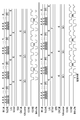
- FIG. 2 is a diagram showing delays of various signals.
- the DCLK, SA [1: 0], LAT, LOAD, STB, GSCLK and GScounter signals in the upper part of FIG. 2 are examples of control signals, and when conversion by the serializer 23 and the deserializer 31 is not performed, It is a waveform input to the drive IC 32.
- the signals of COM1, COM2 and DO1-256 in the upper part of FIG. 2 are examples of drive signals input to the drive IC 32.
- a delay of several ⁇ [sec] occurs.
- the delayed control signal input to the drive IC 32 is shown at the bottom of FIG. The delay time is between the two broken lines in FIG.
- the control signal and the drive signal need to be input to the drive IC 32 in a state where the timing is synchronized. Therefore, the control signal is converted by the serializer 23 and the deserializer 31, and when a delay occurs, it is necessary to delay the drive signal at the same time as the delay time of the control signal in order to synchronize the timing. Further, when the drive signal is delayed in order to synchronize the control signal and the drive signal, if the delay time is taken longer than necessary, the drive frequency is lowered by that amount. Therefore, by delaying the drive signal by the time for converting the control signal by the serializer 23 and the deserializer 31, it is possible to prevent the drive frequency from dropping. Specifically, as shown in the lower part of FIG. 2, the signals of COM1, COM2 and DO1-256 are delayed by the FPGA 21 by the time corresponding to the delay time of the control signal and input to the drive IC.
- the delay time of the control signal generated by the conversion in the serializer 23 and the deserializer 31 changes depending on the individual difference between the serializer 23 and the deserializer 31, the length of the FPC 4, the usage environment, the usage time, and the like. Therefore, in order to make the delay time of the drive signal the same as the delay time of the control signal, the reference signal 26 shown in FIG. 1 is used.
- the reference signal 26 is output from the FPGA 21 together with the control signal in a parallel signal system, and is input to the serializer 23.
- the reference signal 26 is serially converted together with the control signal in the serializer 23, and is input to the deserializer 31 via the FPC 4.
- the reference signal 26 is parallel-converted and output together with the control signal in the deserializer 31.
- the reference signal 26 output from the deserializer 31 is input to the FPGA 21 via the FPC 4. Therefore, the reference signal 26 has a delay in conversion by the serializer 23 and the deserializer 31, similar to the control signal.
- the delay time of the control signal and the delay time of the reference signal 26 are equivalent.
- the FPGA 21 determines the delay time of the drive signal based on the delay time of the reference signal 26, and outputs the delayed signal to the drive signal generation circuit 24.
- the FPGA 21 functions as a delay means and a determination means. The timing is synchronized by inputting the control signal delayed by the conversion in the serializer 23 and the deserializer 31 and the drive signal set to be delayed by the FPGA 21 to the drive IC 32.
- the inkjet recording device 1 of the present embodiment is connected to the drive board 2 that outputs a control signal and a drive signal for ejecting ink from a plurality of nozzles, respectively, via a cable 4.
- An inkjet recording device 1 including an inkjet head 3 that ejects ink from a nozzle based on a control signal output from the drive board 2 and a drive signal, the drive board 2 generates a control signal and a drive signal.
- the inkjet head 3 includes a generation means (FPGA 21, drive signal generation circuit 24), and the inkjet head 3 includes a conversion means (deserializer 31) that converts a control signal received via the cable 4 from a serial signal to a parallel signal, and the cable 4.
- a drive means for driving an actuator for ejecting ink by inputting a drive signal received via A delay means (FPGA21) for delaying only the delay time is provided. Therefore, the control signal in the form of a serial signal transmitted from the drive board 2 to the inkjet head 3 and the drive signal can be suitably synchronized.
- FIG. 3 is a diagram showing an inkjet recording device 1 according to a modification 1. Hereinafter, the difference from FIG. 1 showing the inkjet recording apparatus 1 of the above embodiment will be mainly described.
- the drive board 2 has two serializers 23a and 23b. Further, the inkjet head 3 has two deserializers 31a and 31b corresponding to the serializers 23a and 23b.
- the serializer 23 and the deserializer 31 are configured in twos each, but the configuration is not limited to this. It may be configured to have three or more each.
- the serializer 23a serially converts a part of the control signal of the parallel signal system output from the FPGA 21 and the reference signal 26a.
- the control signal and the reference signal 26a serially converted by the serializer 23a are input to the deserializer 31a via the FPC 4.
- the deserializer 31a converts the input serially converted control signal and reference signal 26a in parallel.
- the control signal and the reference signal 26a are delayed in the delay time a by the conversion in the serializer 23a and the deserializer 31a.
- the control signal converted in parallel is input to the drive IC 32.
- the parallel-converted reference signal 26a is input to the FPGA 21 via the FPC 4.
- the serializer 23b serially converts a part of the control signal of the parallel signal system output from the FPGA 21 and the reference signal 26b.
- the control signal and the reference signal 26b serially converted by the serializer 23b are input to the deserializer 31b via the FPC 4.
- the deserializer 31b parallel-converts the input serially converted control signal and reference signal 26b.
- the control signal and the reference signal 26b are delayed by the delay time b due to the conversion in the serializer 23b and the deserializer 31b.
- the control signal converted in parallel is input to the drive IC 32.
- the parallel-converted reference signal 26b is input to the FPGA 21 via the FPC 4.
- the FPGA 21 compares the delay time a indicated by the input reference signal 26a with the delay time b indicated by the reference signal 26b, and determines the delay time of the drive signal based on the longer time.
- the control signal in the form of a serial signal transmitted from the drive board to the inkjet head is used.
- the drive signal can be suitably synchronized.
- FIG. 4 is a diagram showing an inkjet recording device 1 according to a modification 2.
- FIG. 4 shows the difference from FIG. 1 showing the inkjet recording apparatus 1 of the above embodiment will be mainly described.
- the drive board 2 has two serializers 23a and 23b and two drive signal generation circuits 24a and 24b.
- the inkjet head 3a is connected to the drive substrate 2 via the FPC 4a
- the inkjet head 3b is connected to the drive substrate 2 via the FPC 4b.
- the serializer 23a and the drive signal generation circuit 24a correspond to the inkjet head 3a
- the serializer 23b and the drive signal generation circuit 24b correspond to the inkjet head 3b.
- the number of inkjet heads connected to the drive substrate 2 is two, but the number is not limited to this. Three or more inkjet heads may be connected.
- the inkjet head 3a includes a deserializer 31a, a drive IC 32a, an actuator 33a, a nozzle row 34a, and the like.
- the inkjet head 3b includes a deserializer 31b, a drive IC 32b, an actuator 33b, a nozzle row 34b, and the like.
- the serializer 23a serially converts a part of the control signal of the parallel signal system output from the FPGA 21 and the reference signal 26a.
- the control signal and the reference signal 26a serially converted by the serializer 23a are input to the deserializer 31a via the FPC 4a.
- the deserializer 31a converts the input serially converted control signal and reference signal 26a in parallel.
- the control signal and the reference signal 26a are delayed in the delay time a by the conversion in the serializer 23a and the deserializer 31a.
- the control signal converted in parallel is input to the drive IC 32a.
- the parallel-converted reference signal 26a is input to the FPGA 21 via the FPC4a.
- the serializer 23b serially converts a part of the control signal of the parallel signal system output from the FPGA 21 and the reference signal 26b.
- the control signal and the reference signal 26b serially converted by the serializer 23b are input to the deserializer 31b via the FPC 4b.
- the deserializer 31b parallel-converts the input serially converted control signal and reference signal 26b.
- the control signal and the reference signal 26b are delayed by the delay time b due to the conversion in the serializer 23b and the deserializer 31b.
- the parallel-converted control signal is input to the drive IC 32b.
- the parallel-converted reference signal 26b is input to the FPGA 21 via the FPC4b.
- the delay time of the drive signal for driving the actuators 33a and 33b needs to be unified among the inkjet heads driven by the same drive substrate 2. Therefore, the FPGA 21 compares the delay time a indicated by the input reference signal 26a with the delay time b indicated by the reference signal 26b, and determines the delay time of the drive signal based on the longer time.
- control signal in the form of a serial signal transmitted from the drive board to the inkjet head and the drive signal are suitably synchronized. be able to.
- the determination of the delay time of the drive signal in the above-described embodiment and modification may be performed after the power is turned on to the inkjet recording device 1, or may be performed periodically.
- the delay time of the drive signal is determined based on the delay time of the reference signal 26, but the present invention is not limited to this.
- Printing may be performed by the inkjet recording apparatus 1, the amount of deviation in printing timing may be calculated from the read data obtained by reading the printing result, and the delay time of the drive signal required for timing synchronization with the control signal may be determined from the amount of deviation. ..
- the FPGA 21 determines the delay time of the drive signal based on the delay time of the reference signal 26 as the determination means, but the present invention is not limited to this.
- An external device such as a computer connected via the input / output interface 22 may determine the delay time of the drive signal.
- the delay time information of the reference signal 26 is output to an external device via the FPGA 21 and the input / output interface 22, and is used to determine the delay time of the drive signal. Therefore, in this case, the external device is also included in the inkjet recording device 1. Further, the delay time may be a predetermined fixed value.
- the FPGA 21 performs arithmetic processing, performs various control processing related to the image recording operation in the inkjet recording device 1, and also performs various control processing related to the image recording operation in the inkjet recording device 1, and the delay time of the drive signal is based on the delay time of the reference signal 26.
- It has a CPU (Central Processing Unit) together with the FPGA, and the FPGA and the CPU perform arithmetic processing, perform various control processing related to the image recording operation in the inkjet recording device 1, and drive signals based on the delay time of the reference signal 26.
- the delay time of may be determined.
- the CPU may be configured to function as a delay means by executing a program.
- the present invention can be used for an inkjet recording device and a program for controlling an inkjet recording device.
- Inkjet recording device 2 Drive board 21 FPGA (generation means, delay means) 22 Input / output interface 23, 23a, 23b Serializer 24, 24a, 24b Drive signal generation circuit (generation means) 25 Unit control unit 26, 26a, 26b Reference signal 3, 3a, 3b Inkjet head 31, 31a, 31b Deserializer (conversion means) 32a, 32b drive IC (drive means) 33, 33a, 33b Actuator 34, 34a, 34b Nozzle row 4, 4a, 4b FPC (cable)
Landscapes
- Ink Jet (AREA)
- Particle Formation And Scattering Control In Inkjet Printers (AREA)
Abstract
駆動基板からインクジェットヘッドに送信されるシリアル信号形式の制御信号と駆動信号とを好適に同期をさせることができる。 インクジェット記録装置1は、制御信号及び駆動信号を出力する駆動基板2と、駆動基板2にケーブル4を介して接続され、駆動基板2から出力される制御信号及び駆動信号に基づいてノズルからインクを吐出させるインクジェットヘッド3と、を備え、駆動基板は、制御信号及び駆動信号を生成する生成手段(FPGA21、駆動信号生成回路24)を備え、インクジェットヘッド3は、制御信号をシリアル信号からパラレル信号に変換する変換手段(デシリアライザー31)と、駆動信号とパラレル変換された制御信号の入力によりアクチュエーターを駆動させる駆動手段(駆動IC32)と、を備え、駆動信号を、変換手段における制御信号の遅延時間だけ遅延させる遅延手段(FPGA21)を備える。
Description
この発明は、インクジェット記録装置及びプログラムに関する。
従来、ノズルからインクを吐出させて媒体上に画像や構造などを形成するインクジェット記録装置がある。インクジェット記録装置では、各ノズルに連通するインク流路においてインクに圧力変化を付与することで適切な量のインクを所望の速度で吐出させている。
インクへの圧力付与の方法の一つとして、圧電素子などのアクチュエーターに所定の駆動波形電圧を印加することでインク流路中の圧力室の壁面を変形させる技術がある。アクチュエーターは、印加された電圧に対して高速かつ高精度に変形するので、吐出タイミングや吐出量の制御を精密に行うことができる。
近年、インクジェット記録装置の高速化や高精度化の要求に従って、ノズル及びこれに対応するアクチュエーターの数が増加傾向にある。これに伴い、インクを吐出するノズルに対応するアクチュエーターを選択する駆動ICの数も増える。したがって、駆動ICの制御信号数、インクジェットヘッドのコネクタのピン数、及びケーブル本数が増えるので、プリンターの配線の引き回しが難しくなる。また、信号のクロストークによるノイズ誤動作などの問題もある。
これに対して、制御信号をシリアル変換して送信する事で、インクジェットヘッドのコネクタのピン数を減らす対策が考えられる。
また、プリントヘッドにシリアル通信でデータを送信する技術として、特許文献1には、標準コンピューターとプリントヘッドを、ユニバーサルシリアルバス(USB)を介して、直接接続する技術が記載されている。
これに対して、制御信号をシリアル変換して送信する事で、インクジェットヘッドのコネクタのピン数を減らす対策が考えられる。
また、プリントヘッドにシリアル通信でデータを送信する技術として、特許文献1には、標準コンピューターとプリントヘッドを、ユニバーサルシリアルバス(USB)を介して、直接接続する技術が記載されている。
しかしながら、アクチュエーターを駆動する駆動信号は複雑な波形のため、作成するには回路面積が必要で、発熱も大きいので、駆動基板で作成し、インクジェットヘッドに供給する必要がある。したがって、駆動基板からシリアル信号方式で制御信号を受信し、且つアナログで駆動信号を受信するヘッドインタフェースを持つインクジェットヘッドとした場合、制御信号にはシリアルからパラレルに変換する時間分の遅延が生じるため、駆動信号と同期させることが難しいという問題があった。
この発明の目的は、駆動基板からインクジェットヘッドに送信されるシリアル信号形式の制御信号と駆動信号とを好適に同期をさせることである。
本発明は、上記目的を達成するため、請求項1に記載の発明のインクジェット記録装置は、
複数のノズルから各々インクを吐出させるための制御信号及び駆動信号を出力する駆動基板と、前記駆動基板にケーブルを介して接続され、前記駆動基板から出力される前記制御信号及び前記駆動信号に基づいてノズルからインクを吐出させるインクジェットヘッドと、を備えるインクジェット記録装置であって、
前記駆動基板は、前記制御信号及び前記駆動信号を生成する生成手段を備え、
前記インクジェットヘッドは、
前記ケーブルを介して受信された前記制御信号をシリアル信号からパラレル信号に変換する変換手段と、
前記ケーブルを介して受信された前記駆動信号と前記変換手段によりパラレル変換された前記制御信号の入力によりインクを吐出させるアクチュエーターを駆動させる駆動手段と、を備え、
前記駆動信号を、前記変換手段における前記制御信号の遅延時間だけ遅延させる遅延手段を備える。
また、請求項2記載の発明は、請求項1に記載のインクジェット記録装置において、
前記駆動信号を遅延させる時間を決定する決定手段を備える。
前記駆動信号を遅延させる時間を決定する決定手段を備える。
また、請求項3記載の発明は、請求項2に記載のインクジェット記録装置において、
前記決定手段は、前記制御信号とともに前記駆動基板から前記インクジェットヘッドに受信されて前記変換手段において変換された基準信号に基づいて前記駆動信号を遅延させる時間を決定する。
前記決定手段は、前記制御信号とともに前記駆動基板から前記インクジェットヘッドに受信されて前記変換手段において変換された基準信号に基づいて前記駆動信号を遅延させる時間を決定する。
また、請求項4記載の発明は、請求項2に記載のインクジェット記録装置において、
前記決定手段は、印字結果に基づいて前記駆動信号を遅延させる時間を決定する。
前記決定手段は、印字結果に基づいて前記駆動信号を遅延させる時間を決定する。
また、請求項5記載の発明は、請求項1から4のいずれか一項に記載のインクジェット記録装置において、
複数の前記変換手段を備え、
前記遅延手段は、前記駆動信号を遅延させる時間を、複数の前記変換手段における前記制御信号の遅延時間のうち最大のものに統一する。
複数の前記変換手段を備え、
前記遅延手段は、前記駆動信号を遅延させる時間を、複数の前記変換手段における前記制御信号の遅延時間のうち最大のものに統一する。
また、請求項6記載の発明は、請求項1から4のいずれか一項に記載のインクジェット記録装置において、
複数のインクジェットヘッドを有し、
前記遅延手段は、前記駆動信号を遅延させる時間を、前記複数のインクジェットヘッドの前記変換手段における前記制御信号の遅延時間のうち最大のものに統一する。
複数のインクジェットヘッドを有し、
前記遅延手段は、前記駆動信号を遅延させる時間を、前記複数のインクジェットヘッドの前記変換手段における前記制御信号の遅延時間のうち最大のものに統一する。
また、請求項7記載の発明のプログラムは、
複数のノズルから各々インクを吐出させるための制御信号及び駆動信号を出力する駆動基板と、前記駆動基板にケーブルを介して接続され、前記駆動基板から出力される前記制御信号及び前記駆動信号に基づいてノズルからインクを吐出させるインクジェットヘッドと、を備えるインクジェット記録装置であって、
前記駆動基板は、前記制御信号及び前記駆動信号を生成する生成手段を備え、
前記インクジェットヘッドは、
前記ケーブルを介して受信された前記制御信号をシリアル信号からパラレル信号に変換する変換手段と、
前記ケーブルを介して受信された前記駆動信号と前記変換手段によりパラレル変換された前記制御信号の入力によりインクを吐出させるアクチュエーターを駆動させる駆動手段と、を備えるインクジェット記録装置のコンピューターを、
前記駆動信号を、前記変換手段における前記制御信号の遅延時間だけ遅延させる遅延手段として機能させる。
本発明に従うと、駆動基板からインクジェットヘッドに送信されるシリアル信号形式の制御信号と駆動信号とを好適に同期をさせることができる。
以下、本発明の実施の形態を図面に基づいて説明する。
図1は、インクジェット記録装置1の機能構成を示すブロック図である。
インクジェット記録装置1は、駆動基板2と、インクジェットヘッド3とを備える。ここでは、インクジェットヘッド3として1つのみが示されているが、インクジェット記録装置1が複数のインク色を吐出させるカラープリンターである場合には、インクジェットヘッド3は、当該複数のインク色(例えば、イエロー、マゼンタ、シアン、ブラックの4色)にそれぞれ対応して設けられる。また、同色のインク吐出に係るインクジェットヘッド3を複数設けて更にノズル数を増やしても良い。駆動基板2とインクジェットヘッド3との間は、例えば、ケーブルとしてのFPC4(Flexible Printed Circuit)などで接続されている。
インクジェット記録装置1は、駆動基板2と、インクジェットヘッド3とを備える。ここでは、インクジェットヘッド3として1つのみが示されているが、インクジェット記録装置1が複数のインク色を吐出させるカラープリンターである場合には、インクジェットヘッド3は、当該複数のインク色(例えば、イエロー、マゼンタ、シアン、ブラックの4色)にそれぞれ対応して設けられる。また、同色のインク吐出に係るインクジェットヘッド3を複数設けて更にノズル数を増やしても良い。駆動基板2とインクジェットヘッド3との間は、例えば、ケーブルとしてのFPC4(Flexible Printed Circuit)などで接続されている。
駆動基板2は、FPGA21(Field-Programmable Gate Array)と、入出力インターフェイス22と、シリアライザー23と、駆動信号生成回路24と、ユニット制御部25、メモリー(図示なし)などを備える。
FPGA21は、演算処理を行い、インクジェット記録装置1における画像記録動作に係る各種制御処理を行う。
具体的には、FPGA21は、インクジェットヘッド3の複数のノズルから各々インクを吐出させるためのデジタル形式の制御信号及び駆動信号を生成する。
制御信号には、画素データの転送や駆動信号の供給などの動作可否や動作タイミングの制御を行うための信号が含まれる。
具体的には、FPGA21は、インクジェットヘッド3の複数のノズルから各々インクを吐出させるためのデジタル形式の制御信号及び駆動信号を生成する。
制御信号には、画素データの転送や駆動信号の供給などの動作可否や動作タイミングの制御を行うための信号が含まれる。
入出力インターフェイス22は、外部装置から画像記録に係る命令、設定や記録対象の画像データを受け取り、また、FPGA21から外部装置に対して画像記録動作に係るステータスや異常発生情報などを出力するためのインターフェイスである。入出力インターフェイス22としては、ネットワークカード(LANカード)などが用いられる。
シリアライザー23は、FPGA21から出力されたパラレル信号方式の各種制御信号をシリアル変換する。
シリアル変換された制御信号は、駆動基板2とインクジェットヘッド3を接続するFPC4を介して、インクジェットヘッド3内のデシリアライザー31に出力される。
シリアル変換された制御信号は、駆動基板2とインクジェットヘッド3を接続するFPC4を介して、インクジェットヘッド3内のデシリアライザー31に出力される。
駆動信号生成回路24は、FPGA21から出力されたデジタル信号をアナログ信号に変換後、増幅し、駆動信号を生成する。
生成された駆動信号は、FPC4を介して、インクジェットヘッド3内の駆動IC32に出力され、インクジェットヘッド3内のアクチュエーター33を駆動するために用いられる。
よって、FPGA21及び駆動信号生成回路24は、生成手段として機能する。
生成された駆動信号は、FPC4を介して、インクジェットヘッド3内の駆動IC32に出力され、インクジェットヘッド3内のアクチュエーター33を駆動するために用いられる。
よって、FPGA21及び駆動信号生成回路24は、生成手段として機能する。
ユニット制御部25は、インクジェット記録装置1の全体動作の統括制御を行う。
メモリー(図示なし)は、外部装置から取得された記録対象の画像データや、当該画像データから生成された各ノズルからのインク吐出状態を定める画素データを記憶する。メモリー(図示なし)からは、画素データがインクジェットヘッド3の駆動IC32に出力されて、インクを吐出するノズルを選択するのに用いられる。
インクジェットヘッド3はデシリアライザー31と、駆動IC32と、アクチュエーター33、ノズル列34などを有する。
デシリアライザー31は、シリアライザー23から出力されたシリアル信号方式の制御信号をパラレル信号方式に変換する。ここで、デシリアライザー31は、変換手段として機能する。
パラレル変換された制御信号は、駆動IC32に出力される。
パラレル変換された制御信号は、駆動IC32に出力される。
駆動IC32は、駆動信号生成回路24から出力された駆動信号、デシリアライザー31から出力された制御信号、及びメモリー(図示なし)から出力された画像データを入力する。
駆動IC32は、画像データや制御信号に基づいて、アクチュエーター33を適切なタイミング、振幅及び期間で変形させるための駆動信号を、選択されたノズルに対応するアクチュエーター33に出力する。
よって、駆動IC32は、駆動手段として機能する。
駆動IC32は、画像データや制御信号に基づいて、アクチュエーター33を適切なタイミング、振幅及び期間で変形させるための駆動信号を、選択されたノズルに対応するアクチュエーター33に出力する。
よって、駆動IC32は、駆動手段として機能する。
アクチュエーター33は、各ノズルに連通してインクを供給するチャネル(インク流路)ごとにインクを吐出させたり、インクを吐出させずに液面(メニスカス)を振動させたりするための圧力変化をインクに付与する。アクチュエーター33としては、ここでは、PZT(チタン酸ジルコン酸鉛)といった圧電素子が用いられ、この圧電素子が、一次元配列されたチャネルの隔壁として各チャネル間に配置される。アクチュエーターの両側面(すなわち、チャネルの内側面)に設けられた電極膜を介してアクチュエーターに所定の電圧が印加されることで、当該アクチュエーターが屈曲変形し、内部のインクに圧力を付与する。なお、一次元配列されたチャネルの両端には、当該両端のチャネルに対して屈曲変形の影響を与えるためのダミーチャネルが設けられ、インクが供給、吐出されずに変形動作がなされる。アクチュエーターの変形には、ここでは、せん断モード(シアモード)が用いられるが、ベンドモードなど他のモードでの変形が利用されても良い。
ノズル列34は、適宜パターンで配列された2以上の所定数のノズルを有する。
アクチュエーター33及びノズル列34は、それぞれ一つのブロックとして構成されているが、複数のブロックに分けて構成されてもよい。
図2は、各種信号の遅延を示す図である。
図2の上部のDCLK、SA[1:0]、LAT、LOAD、STB、GSCLK及びGScounterの信号は、制御信号の例であり、シリアライザー23及びデシリアライザー31による変換を行わない場合に、駆動IC32に入力される波形である。
また、図2の上部のCOM1、COM2及びDO1-256の信号は、駆動IC32に入力される駆動信号の例である。
制御信号をシリアライザー23及びデシリアライザー31で変換を行うと、数μ[sec]の遅延が生じる。駆動IC32に入力される遅延が生じた制御信号を図2の下部に示す。図2の2本の破線間が遅延時間である。
制御信号と駆動信号はタイミングが同期されている状態で駆動IC32に入力される必要がある。そのため、制御信号をシリアライザー23及びデシリアライザー31で変換を行い、遅延が生じた場合、タイミングを同期させるため、駆動信号も制御信号の遅延時間と同時間の遅延をさせる必要がある。
また、制御信号と駆動信号を同期させるために駆動信号を遅延させる際、遅延時間を必要以上に取ると、その分駆動周波数が落ちる。そのため、制御信号をシリアライザー23及びデシリアライザー31で変換する時間分だけ駆動信号を遅延させる事で、駆動周波数が落ちるのを防ぐことができる。
具体的には、図2の下部に示すように、COM1、COM2及びDO1-256の信号は、FPGA21により制御信号の遅延時間に対応する時間分だけ遅延されて駆動ICに入力される。
シリアライザー23及びデシリアライザー31での変換で生じる制御信号の遅延時間は、シリアライザー23及びデシリアライザー31の個体差、FPC4の長さ、使用環境や使用時間等で変化する。
そこで、駆動信号の遅延時間を制御信号の遅延時間と同一にするために、図1に示す基準信号26を用いる。
基準信号26は、FPGA21から制御信号とともにパラレル信号方式で出力され、シリアライザー23に入力される。次いで、基準信号26は、シリアライザー23において、制御信号とともにシリアル変換され、FPC4を介して、デシリアライザー31に入力される。次いで、基準信号26は、デシリアライザー31において、制御信号とともにパラレル変換され出力される。デシリアライザー31から出力された基準信号26は、FPC4を介して、FPGA21に入力される。
したがって、基準信号26には、制御信号と同様にシリアライザー23及びデシリアライザー31での変換で遅延が生じる。制御信号の遅延時間と基準信号26の遅延時間は同等である。
FPGA21は、基準信号26の遅延時間に基づいて、駆動信号の遅延時間を決定し、遅延させた信号を駆動信号生成回路24に出力する。ここで、FPGA21は、遅延手段及び決定手段として機能する。
シリアライザー23及びデシリアライザー31での変換で遅延した制御信号とFPGA21で遅延を設定された駆動信号が、駆動IC32に入力されることによってタイミングが同期される。
以上のように、本実施形態のインクジェット記録装置1は、複数のノズルから各々インクを吐出させるための制御信号及び駆動信号を出力する駆動基板2と、駆動基板2にケーブル4を介して接続され、駆動基板2から出力される制御信号及び駆動信号に基づいてノズルからインクを吐出させるインクジェットヘッド3と、を備えるインクジェット記録装置1であって、駆動基板2は、制御信号及び駆動信号を生成する生成手段(FPGA21、駆動信号生成回路24)を備え、インクジェットヘッド3は、ケーブル4を介して受信された制御信号をシリアル信号からパラレル信号に変換する変換手段(デシリアライザー31)と、ケーブル4を介して受信された駆動信号と変換手段によりパラレル変換された制御信号の入力によりインクを吐出させるアクチュエーターを駆動させる駆動手段(駆動IC32)と、を備え、駆動信号を、変換手段における制御信号の遅延時間だけ遅延させる遅延手段(FPGA21)を備える。
従って、駆動基板2からインクジェットヘッド3に送信されるシリアル信号形式の制御信号と駆動信号とを好適に同期をさせることができる。
従って、駆動基板2からインクジェットヘッド3に送信されるシリアル信号形式の制御信号と駆動信号とを好適に同期をさせることができる。
(変形例1)
図3は、変形例1に係るインクジェット記録装置1を示す図である。以下では、上記実施形態のインクジェット記録装置1を示す図1との差異を中心に説明する。
図3は、変形例1に係るインクジェット記録装置1を示す図である。以下では、上記実施形態のインクジェット記録装置1を示す図1との差異を中心に説明する。
本変形例1の構成では、駆動基板2は二つのシリアライザー23a、23bを有する。また、インクジェットヘッド3はシリアライザー23a、23bに対応する二つのデシリアライザー31a、31bを有する。
ここでは、シリアライザー23及びデシリアライザー31は二つずつの構成にしたが、これに限らない。それぞれ三つ以上を有する構成としてもよい。
ここでは、シリアライザー23及びデシリアライザー31は二つずつの構成にしたが、これに限らない。それぞれ三つ以上を有する構成としてもよい。
シリアライザー23aは、FPGA21から出力されたパラレル信号方式の制御信号の一部及び基準信号26aをシリアル変換する。
シリアライザー23aによってシリアル変換された制御信号及び基準信号26aは、FPC4を介して、デシリアライザー31aに入力される。
デシリアライザー31aは、入力されたシリアル変換された制御信号及び基準信号26aをパラレル変換する。
制御信号及び基準信号26aには、シリアライザー23a及びデシリアライザー31aにおける変換で遅延時間aの遅延が生じる。
パラレル変換された制御信号は、駆動IC32に入力される。
パラレル変換された基準信号26aは、FPC4を介して、FPGA21に入力される。
シリアライザー23aによってシリアル変換された制御信号及び基準信号26aは、FPC4を介して、デシリアライザー31aに入力される。
デシリアライザー31aは、入力されたシリアル変換された制御信号及び基準信号26aをパラレル変換する。
制御信号及び基準信号26aには、シリアライザー23a及びデシリアライザー31aにおける変換で遅延時間aの遅延が生じる。
パラレル変換された制御信号は、駆動IC32に入力される。
パラレル変換された基準信号26aは、FPC4を介して、FPGA21に入力される。
同様に、シリアライザー23bは、FPGA21から出力されたパラレル信号方式の制御信号の一部及び基準信号26bをシリアル変換する。
シリアライザー23bによってシリアル変換された制御信号及び基準信号26bは、FPC4を介して、デシリアライザー31bに入力される。
デシリアライザー31bは、入力されたシリアル変換された制御信号及び基準信号26bをパラレル変換する。
制御信号及び基準信号26bには、シリアライザー23b及びデシリアライザー31bにおける変換で遅延時間bの遅延が生じる。
パラレル変換された制御信号は、駆動IC32に入力される。
パラレル変換された基準信号26bは、FPC4を介して、FPGA21に入力される。
シリアライザー23bによってシリアル変換された制御信号及び基準信号26bは、FPC4を介して、デシリアライザー31bに入力される。
デシリアライザー31bは、入力されたシリアル変換された制御信号及び基準信号26bをパラレル変換する。
制御信号及び基準信号26bには、シリアライザー23b及びデシリアライザー31bにおける変換で遅延時間bの遅延が生じる。
パラレル変換された制御信号は、駆動IC32に入力される。
パラレル変換された基準信号26bは、FPC4を介して、FPGA21に入力される。
FPGA21は、入力された基準信号26aが示す遅延時間aと基準信号26bが示す遅延時間bを比較し、時間が長い方に基づいて駆動信号の遅延時間を決定する。
以上のように、駆動基板2が複数のシリアライザー23を有し、インクジェットヘッド3が複数のデシリアライザー31を有する場合においても、駆動基板からインクジェットヘッドに送信されるシリアル信号形式の制御信号と駆動信号とを好適に同期をさせることができる。
(変形例2)
図4は、変形例2に係るインクジェット記録装置1を示す図である。以下では、上記実施形態のインクジェット記録装置1を示す図1との差異を中心に説明する。
図4は、変形例2に係るインクジェット記録装置1を示す図である。以下では、上記実施形態のインクジェット記録装置1を示す図1との差異を中心に説明する。
本変形例2の構成では、駆動基板2は二つのシリアライザー23a、23bと二つの駆動信号生成回路24a、24bを有する。
また、駆動基板2には、FPC4aを介して、インクジェットヘッド3aが接続され、同様に、FPC4bを介して、インクジェットヘッド3bが接続されている。
シリアライザー23a及び駆動信号生成回路24aは、インクジェットヘッド3aに対応しており、シリアライザー23b及び駆動信号生成回路24bは、インクジェットヘッド3bに対応している。
ここで、駆動基板2に接続されているインクジェットヘッドは二つとしたが、これに限らない。三つ以上のインクジェットヘッドが接続されていてもよい。
また、駆動基板2には、FPC4aを介して、インクジェットヘッド3aが接続され、同様に、FPC4bを介して、インクジェットヘッド3bが接続されている。
シリアライザー23a及び駆動信号生成回路24aは、インクジェットヘッド3aに対応しており、シリアライザー23b及び駆動信号生成回路24bは、インクジェットヘッド3bに対応している。
ここで、駆動基板2に接続されているインクジェットヘッドは二つとしたが、これに限らない。三つ以上のインクジェットヘッドが接続されていてもよい。
インクジェットヘッド3aは、デシリアライザー31a、駆動IC32a、アクチュエーター33a及びノズル列34a等を有する。
インクジェットヘッド3bは、デシリアライザー31b、駆動IC32b、アクチュエーター33b及びノズル列34b等を有する。
インクジェットヘッド3bは、デシリアライザー31b、駆動IC32b、アクチュエーター33b及びノズル列34b等を有する。
シリアライザー23aは、FPGA21から出力されたパラレル信号方式の制御信号の一部及び基準信号26aをシリアル変換する。
シリアライザー23aによってシリアル変換された制御信号及び基準信号26aは、FPC4aを介して、デシリアライザー31aに入力される。
デシリアライザー31aは、入力されたシリアル変換された制御信号及び基準信号26aをパラレル変換する。
制御信号及び基準信号26aには、シリアライザー23a及びデシリアライザー31aにおける変換で遅延時間aの遅延が生じる。
パラレル変換された制御信号は、駆動IC32aに入力される。
パラレル変換された基準信号26aは、FPC4aを介して、FPGA21に入力される。
シリアライザー23aによってシリアル変換された制御信号及び基準信号26aは、FPC4aを介して、デシリアライザー31aに入力される。
デシリアライザー31aは、入力されたシリアル変換された制御信号及び基準信号26aをパラレル変換する。
制御信号及び基準信号26aには、シリアライザー23a及びデシリアライザー31aにおける変換で遅延時間aの遅延が生じる。
パラレル変換された制御信号は、駆動IC32aに入力される。
パラレル変換された基準信号26aは、FPC4aを介して、FPGA21に入力される。
同様に、シリアライザー23bは、FPGA21から出力されたパラレル信号方式の制御信号の一部及び基準信号26bをシリアル変換する。
シリアライザー23bによってシリアル変換された制御信号及び基準信号26bは、FPC4bを介して、デシリアライザー31bに入力される。
デシリアライザー31bは、入力されたシリアル変換された制御信号及び基準信号26bをパラレル変換する。
制御信号及び基準信号26bには、シリアライザー23b及びデシリアライザー31bにおける変換で遅延時間bの遅延が生じる。
パラレル変換された制御信号は、駆動IC32bに入力される。
パラレル変換された基準信号26bは、FPC4bを介して、FPGA21に入力される。
シリアライザー23bによってシリアル変換された制御信号及び基準信号26bは、FPC4bを介して、デシリアライザー31bに入力される。
デシリアライザー31bは、入力されたシリアル変換された制御信号及び基準信号26bをパラレル変換する。
制御信号及び基準信号26bには、シリアライザー23b及びデシリアライザー31bにおける変換で遅延時間bの遅延が生じる。
パラレル変換された制御信号は、駆動IC32bに入力される。
パラレル変換された基準信号26bは、FPC4bを介して、FPGA21に入力される。
アクチュエーター33a、33bを駆動する駆動信号の遅延時間は、同一の駆動基板2で駆動されるインクジェットヘッド間で統一される必要がある。
そのため、FPGA21は、入力された基準信号26aが示す遅延時間aと基準信号26bが示す遅延時間bを比較し、時間が長い方に基づいて駆動信号の遅延時間を決定する。
そのため、FPGA21は、入力された基準信号26aが示す遅延時間aと基準信号26bが示す遅延時間bを比較し、時間が長い方に基づいて駆動信号の遅延時間を決定する。
以上のように、一つの駆動基板2に複数のインクジェットヘッド3が接続されている場合においても、駆動基板からインクジェットヘッドに送信されるシリアル信号形式の制御信号と駆動信号とを好適に同期をさせることができる。
上記実施の形態及び変形例における、駆動信号の遅延時間の決定は、インクジェット記録装置1への電源投入後に行ってもよいし、定期的に実施されてもよい。
なお、本発明は、上記実施の形態に限られるものではなく、様々な変更が可能である。
例えば、上記実施の形態及び変形例では、駆動信号の遅延時間を基準信号26の遅延時間に基づいて決定するとしたが、これに限らない。インクジェット記録装置1で印字を行い、印字結果を読み取った読み取りデータから印字タイミングのずれ量を算出し、かかるずれ量から制御信号とのタイミング同期に必要な駆動信号の遅延時間を決定してもよい。
例えば、上記実施の形態及び変形例では、駆動信号の遅延時間を基準信号26の遅延時間に基づいて決定するとしたが、これに限らない。インクジェット記録装置1で印字を行い、印字結果を読み取った読み取りデータから印字タイミングのずれ量を算出し、かかるずれ量から制御信号とのタイミング同期に必要な駆動信号の遅延時間を決定してもよい。
また、上記実施の形態及び変形例では、決定手段としてFPGA21が基準信号26の遅延時間に基づいて、駆動信号の遅延時間を決定するとしたがこれに限らない。入出力インターフェイス22を介して接続されているコンピューター等の外部装置が駆動信号の遅延時間を決定してもよい。この場合、基準信号26の遅延時間情報はFPGA21及び入出力インターフェイス22を介して、外部装置に出力され、駆動信号の遅延時間の決定に用いられる。よって、この場合、外部装置もインクジェット記録装置1に含まれる。
また、遅延時間は予め定められた固定値でもよい。
また、遅延時間は予め定められた固定値でもよい。
また、上記実施の形態及び変形例では、FPGA21が演算処理を行い、インクジェット記録装置1における画像記録動作に係る各種制御処理を行い、また基準信号26の遅延時間に基づいて、駆動信号の遅延時間を決定するとしたがこれに限らない。FPGAとともにCPU(Central Processing Unit)を有し、FPGA及びCPUが演算処理を行い、インクジェット記録装置1における画像記録動作に係る各種制御処理を行い、また基準信号26の遅延時間に基づいて、駆動信号の遅延時間を決定するとしてもよい。
また、CPUがプログラムを実行することにより遅延手段として機能するように構成してもよい。
また、CPUがプログラムを実行することにより遅延手段として機能するように構成してもよい。
その他、上記実施の形態で示した構成、回路配置や動作手順などの具体的な細部は、本発明の趣旨を逸脱しない範囲において適宜変更可能である。
この発明は、インクジェット記録装置及びインクジェット記録装置を制御するプログラムに利用することができる。
1 インクジェット記録装置
2 駆動基板
21 FPGA(生成手段、遅延手段)
22 入出力インターフェイス
23、23a、23b シリアライザー
24、24a、24b 駆動信号生成回路(生成手段)
25 ユニット制御部
26、26a、26b 基準信号
3、3a、3b インクジェットヘッド
31、31a、31b デシリアライザー(変換手段)
32a、32b 駆動IC(駆動手段)
33、33a、33b アクチュエーター
34、34a、34b ノズル列
4、4a、4b FPC(ケーブル)
2 駆動基板
21 FPGA(生成手段、遅延手段)
22 入出力インターフェイス
23、23a、23b シリアライザー
24、24a、24b 駆動信号生成回路(生成手段)
25 ユニット制御部
26、26a、26b 基準信号
3、3a、3b インクジェットヘッド
31、31a、31b デシリアライザー(変換手段)
32a、32b 駆動IC(駆動手段)
33、33a、33b アクチュエーター
34、34a、34b ノズル列
4、4a、4b FPC(ケーブル)
Claims (7)
- 複数のノズルから各々インクを吐出させるための制御信号及び駆動信号を出力する駆動基板と、前記駆動基板にケーブルを介して接続され、前記駆動基板から出力される前記制御信号及び前記駆動信号に基づいてノズルからインクを吐出させるインクジェットヘッドと、を備えるインクジェット記録装置であって、
前記駆動基板は、前記制御信号及び前記駆動信号を生成する生成手段を備え、
前記インクジェットヘッドは、
前記ケーブルを介して受信された前記制御信号をシリアル信号からパラレル信号に変換する変換手段と、
前記ケーブルを介して受信された前記駆動信号と前記変換手段によりパラレル変換された前記制御信号の入力によりインクを吐出させるアクチュエーターを駆動させる駆動手段と、を備え、
前記駆動信号を、前記変換手段における前記制御信号の遅延時間だけ遅延させる遅延手段を備えるインクジェット記録装置。 - 前記駆動信号を遅延させる時間を決定する決定手段を備える請求項1に記載のインクジェット記録装置。
- 前記決定手段は、前記制御信号とともに前記駆動基板から前記インクジェットヘッドに受信されて前記変換手段において変換された基準信号に基づいて前記駆動信号を遅延させる時間を決定する請求項2に記載のインクジェット記録装置。
- 前記決定手段は、印字結果に基づいて前記駆動信号を遅延させる時間を決定する請求項2に記載のインクジェット記録装置。
- 複数の前記変換手段を備え、
前記遅延手段は、前記駆動信号を遅延させる時間を、複数の前記変換手段における前記制御信号の遅延時間のうち最大のものに統一する請求項1から4のいずれか一項に記載のインクジェット記録装置。 - 複数のインクジェットヘッドを有し、
前記遅延手段は、前記駆動信号を遅延させる時間を、前記複数のインクジェットヘッドの前記変換手段における前記制御信号の遅延時間のうち最大のものに統一する請求項1から4のいずれか一項に記載のインクジェット記録装置。 - 複数のノズルから各々インクを吐出させるための制御信号及び駆動信号を出力する駆動基板と、前記駆動基板にケーブルを介して接続され、前記駆動基板から出力される前記制御信号及び前記駆動信号に基づいてノズルからインクを吐出させるインクジェットヘッドと、を備えるインクジェット記録装置であって、
前記駆動基板は、前記制御信号及び前記駆動信号を生成する生成手段を備え、
前記インクジェットヘッドは、
前記ケーブルを介して受信された前記制御信号をシリアル信号からパラレル信号に変換する変換手段と、
前記ケーブルを介して受信された前記駆動信号と前記変換手段によりパラレル変換された前記制御信号の入力によりインクを吐出させるアクチュエーターを駆動させる駆動手段と、を備えるインクジェット記録装置のコンピューターを、
前記駆動信号を、前記変換手段における前記制御信号の遅延時間だけ遅延させる遅延手段として機能させるプログラム。
Priority Applications (2)
| Application Number | Priority Date | Filing Date | Title |
|---|---|---|---|
| PCT/JP2020/023996 WO2021255904A1 (ja) | 2020-06-18 | 2020-06-18 | インクジェット記録装置及びプログラム |
| JP2022531206A JP7468647B2 (ja) | 2020-06-18 | 2020-06-18 | インクジェット記録装置及びプログラム |
Applications Claiming Priority (1)
| Application Number | Priority Date | Filing Date | Title |
|---|---|---|---|
| PCT/JP2020/023996 WO2021255904A1 (ja) | 2020-06-18 | 2020-06-18 | インクジェット記録装置及びプログラム |
Publications (1)
| Publication Number | Publication Date |
|---|---|
| WO2021255904A1 true WO2021255904A1 (ja) | 2021-12-23 |
Family
ID=79267682
Family Applications (1)
| Application Number | Title | Priority Date | Filing Date |
|---|---|---|---|
| PCT/JP2020/023996 WO2021255904A1 (ja) | 2020-06-18 | 2020-06-18 | インクジェット記録装置及びプログラム |
Country Status (2)
| Country | Link |
|---|---|
| JP (1) | JP7468647B2 (ja) |
| WO (1) | WO2021255904A1 (ja) |
Citations (5)
| Publication number | Priority date | Publication date | Assignee | Title |
|---|---|---|---|---|
| JPH10138473A (ja) * | 1996-11-07 | 1998-05-26 | Seiko Epson Corp | プリンタヘッドの駆動回路 |
| JPH11138798A (ja) * | 1997-09-08 | 1999-05-25 | Konica Corp | インクジェットプリンタ |
| JP2000158643A (ja) * | 1998-09-25 | 2000-06-13 | Brother Ind Ltd | 記録装置 |
| US20070070104A1 (en) * | 2005-09-26 | 2007-03-29 | Samsung Electronics Co., Ltd. | Head driving device, inkjet printer comprising the same, and data processing method thereof |
| JP2009045761A (ja) * | 2007-08-14 | 2009-03-05 | Fuji Xerox Co Ltd | 液滴吐出装置 |
-
2020
- 2020-06-18 JP JP2022531206A patent/JP7468647B2/ja active Active
- 2020-06-18 WO PCT/JP2020/023996 patent/WO2021255904A1/ja active Application Filing
Patent Citations (5)
| Publication number | Priority date | Publication date | Assignee | Title |
|---|---|---|---|---|
| JPH10138473A (ja) * | 1996-11-07 | 1998-05-26 | Seiko Epson Corp | プリンタヘッドの駆動回路 |
| JPH11138798A (ja) * | 1997-09-08 | 1999-05-25 | Konica Corp | インクジェットプリンタ |
| JP2000158643A (ja) * | 1998-09-25 | 2000-06-13 | Brother Ind Ltd | 記録装置 |
| US20070070104A1 (en) * | 2005-09-26 | 2007-03-29 | Samsung Electronics Co., Ltd. | Head driving device, inkjet printer comprising the same, and data processing method thereof |
| JP2009045761A (ja) * | 2007-08-14 | 2009-03-05 | Fuji Xerox Co Ltd | 液滴吐出装置 |
Also Published As
| Publication number | Publication date |
|---|---|
| JPWO2021255904A1 (ja) | 2021-12-23 |
| JP7468647B2 (ja) | 2024-04-16 |
Similar Documents
| Publication | Publication Date | Title |
|---|---|---|
| CN114619759B (zh) | 液体喷出装置以及图像形成装置 | |
| JP6488663B2 (ja) | 液体吐出装置および液体吐出モジュール | |
| EP2072260B1 (en) | Head element substrate, recording head, and recording apparatus | |
| JP2008290387A (ja) | 液体吐出装置及び信号伝送路 | |
| US7296865B2 (en) | Liquid ejection method, computer-readable medium, liquid ejection apparatus, and liquid ejection system | |
| US10265955B2 (en) | Liquid discharge apparatus | |
| EP3385079A1 (en) | Driving waveform generating device, liquid discharge head, inkjet recording apparatus, and driving waveform generating method | |
| US7438372B2 (en) | Driver device for recording head | |
| WO2021255904A1 (ja) | インクジェット記録装置及びプログラム | |
| JP2008100483A (ja) | ヘッド基板、記録ヘッド、及び記録装置 | |
| US8857934B2 (en) | Print element substrate, printhead, and printing apparatus | |
| JP6717367B2 (ja) | 液体吐出装置 | |
| JP6217819B2 (ja) | 印刷装置、およびラインヘッドユニット | |
| JP4934997B2 (ja) | 記録装置 | |
| WO2022224295A1 (ja) | 液体吐出装置、プログラム及び液体吐出ヘッド | |
| JP2016150455A (ja) | 液体吐出装置 | |
| CN111746116B (zh) | 液体喷出装置的致动器驱动电路及印刷控制装置 | |
| JP2009154493A (ja) | インクジェットヘッドの駆動方法及び駆動装置 | |
| JP6554965B2 (ja) | 液体吐出装置、および液体吐出装置の制御方法 | |
| JPH03208656A (ja) | インクジェット記録方法,インクジェット記録ヘッドおよびインクジェット記録装置 | |
| JP5803531B2 (ja) | プリントヘッド制御回路、印刷装置、プリントヘッド制御方法、印刷物生産方法、プリントヘッド制御用信号生成送信回路およびプリントヘッドユニット | |
| JP3753075B2 (ja) | インクジェット記録装置 | |
| WO2020217471A1 (ja) | インクジェット記録装置、インクジェット記録装置の調整方法及びインクジェット記録装置の制御方法 | |
| JP2016215524A (ja) | 液体吐出装置 | |
| JP2007131012A (ja) | 記録装置 |
Legal Events
| Date | Code | Title | Description |
|---|---|---|---|
| 121 | Ep: the epo has been informed by wipo that ep was designated in this application |
Ref document number: 20941491 Country of ref document: EP Kind code of ref document: A1 |
|
| ENP | Entry into the national phase |
Ref document number: 2022531206 Country of ref document: JP Kind code of ref document: A |
|
| NENP | Non-entry into the national phase |
Ref country code: DE |
|
| 122 | Ep: pct application non-entry in european phase |
Ref document number: 20941491 Country of ref document: EP Kind code of ref document: A1 |