WO2021245907A1 - 光電子集積モジュール - Google Patents
光電子集積モジュール Download PDFInfo
- Publication number
- WO2021245907A1 WO2021245907A1 PCT/JP2020/022253 JP2020022253W WO2021245907A1 WO 2021245907 A1 WO2021245907 A1 WO 2021245907A1 JP 2020022253 W JP2020022253 W JP 2020022253W WO 2021245907 A1 WO2021245907 A1 WO 2021245907A1
- Authority
- WO
- WIPO (PCT)
- Prior art keywords
- electric
- substrate
- optical
- filler
- optoelectronic
- Prior art date
- Legal status (The legal status is an assumption and is not a legal conclusion. Google has not performed a legal analysis and makes no representation as to the accuracy of the status listed.)
- Ceased
Links
Images



Classifications
-
- H—ELECTRICITY
- H10—SEMICONDUCTOR DEVICES; ELECTRIC SOLID-STATE DEVICES NOT OTHERWISE PROVIDED FOR
- H10W—GENERIC PACKAGES, INTERCONNECTIONS, CONNECTORS OR OTHER CONSTRUCTIONAL DETAILS OF DEVICES COVERED BY CLASS H10
- H10W90/00—Package configurations
-
- G—PHYSICS
- G02—OPTICS
- G02B—OPTICAL ELEMENTS, SYSTEMS OR APPARATUS
- G02B6/00—Light guides; Structural details of arrangements comprising light guides and other optical elements, e.g. couplings
- G02B6/24—Coupling light guides
- G02B6/42—Coupling light guides with opto-electronic elements
- G02B6/4201—Packages, e.g. shape, construction, internal or external details
- G02B6/4219—Mechanical fixtures for holding or positioning the elements relative to each other in the couplings; Alignment methods for the elements, e.g. measuring or observing methods especially used therefor
- G02B6/4228—Passive alignment, i.e. without a detection of the degree of coupling or the position of the elements
- G02B6/423—Passive alignment, i.e. without a detection of the degree of coupling or the position of the elements using guiding surfaces for the alignment
- G02B6/4231—Passive alignment, i.e. without a detection of the degree of coupling or the position of the elements using guiding surfaces for the alignment with intermediate elements, e.g. rods and balls, between the elements
-
- G—PHYSICS
- G02—OPTICS
- G02B—OPTICAL ELEMENTS, SYSTEMS OR APPARATUS
- G02B6/00—Light guides; Structural details of arrangements comprising light guides and other optical elements, e.g. couplings
- G02B6/24—Coupling light guides
- G02B6/42—Coupling light guides with opto-electronic elements
- G02B6/4201—Packages, e.g. shape, construction, internal or external details
- G02B6/4266—Thermal aspects, temperature control or temperature monitoring
- G02B6/4268—Cooling
- G02B6/4269—Cooling with heat sinks or radiation fins
-
- G—PHYSICS
- G02—OPTICS
- G02B—OPTICAL ELEMENTS, SYSTEMS OR APPARATUS
- G02B6/00—Light guides; Structural details of arrangements comprising light guides and other optical elements, e.g. couplings
- G02B6/24—Coupling light guides
- G02B6/42—Coupling light guides with opto-electronic elements
- G02B6/4201—Packages, e.g. shape, construction, internal or external details
- G02B6/4274—Electrical aspects
- G02B6/428—Electrical aspects containing printed circuit boards [PCB]
-
- H—ELECTRICITY
- H05—ELECTRIC TECHNIQUES NOT OTHERWISE PROVIDED FOR
- H05K—PRINTED CIRCUITS; CASINGS OR CONSTRUCTIONAL DETAILS OF ELECTRIC APPARATUS; MANUFACTURE OF ASSEMBLAGES OF ELECTRICAL COMPONENTS
- H05K1/00—Printed circuits
- H05K1/02—Details
- H05K1/0201—Thermal arrangements, e.g. for cooling, heating or preventing overheating
- H05K1/0203—Cooling of mounted components
- H05K1/0204—Cooling of mounted components using means for thermal conduction connection in the thickness direction of the substrate
- H05K1/0206—Cooling of mounted components using means for thermal conduction connection in the thickness direction of the substrate by printed thermal vias
-
- H—ELECTRICITY
- H10—SEMICONDUCTOR DEVICES; ELECTRIC SOLID-STATE DEVICES NOT OTHERWISE PROVIDED FOR
- H10W—GENERIC PACKAGES, INTERCONNECTIONS, CONNECTORS OR OTHER CONSTRUCTIONAL DETAILS OF DEVICES COVERED BY CLASS H10
- H10W40/00—Arrangements for thermal protection or thermal control
- H10W40/20—Arrangements for cooling
- H10W40/22—Arrangements for cooling characterised by their shape, e.g. having conical or cylindrical projections
- H10W40/226—Arrangements for cooling characterised by their shape, e.g. having conical or cylindrical projections characterised by projecting parts, e.g. fins to increase surface area
- H10W40/228—Arrangements for cooling characterised by their shape, e.g. having conical or cylindrical projections characterised by projecting parts, e.g. fins to increase surface area the projecting parts being wire-shaped or pin-shaped
-
- H—ELECTRICITY
- H10—SEMICONDUCTOR DEVICES; ELECTRIC SOLID-STATE DEVICES NOT OTHERWISE PROVIDED FOR
- H10W—GENERIC PACKAGES, INTERCONNECTIONS, CONNECTORS OR OTHER CONSTRUCTIONAL DETAILS OF DEVICES COVERED BY CLASS H10
- H10W72/00—Interconnections or connectors in packages
- H10W72/071—Connecting or disconnecting
- H10W72/072—Connecting or disconnecting of bump connectors
- H10W72/07251—Connecting or disconnecting of bump connectors characterised by changes in properties of the bump connectors during connecting
-
- H—ELECTRICITY
- H10—SEMICONDUCTOR DEVICES; ELECTRIC SOLID-STATE DEVICES NOT OTHERWISE PROVIDED FOR
- H10W—GENERIC PACKAGES, INTERCONNECTIONS, CONNECTORS OR OTHER CONSTRUCTIONAL DETAILS OF DEVICES COVERED BY CLASS H10
- H10W72/00—Interconnections or connectors in packages
- H10W72/20—Bump connectors, e.g. solder bumps or copper pillars; Dummy bumps; Thermal bumps
-
- H—ELECTRICITY
- H10—SEMICONDUCTOR DEVICES; ELECTRIC SOLID-STATE DEVICES NOT OTHERWISE PROVIDED FOR
- H10W—GENERIC PACKAGES, INTERCONNECTIONS, CONNECTORS OR OTHER CONSTRUCTIONAL DETAILS OF DEVICES COVERED BY CLASS H10
- H10W76/00—Containers; Fillings or auxiliary members therefor; Seals
- H10W76/10—Containers or parts thereof
- H10W76/12—Containers or parts thereof characterised by their shape
-
- H—ELECTRICITY
- H10—SEMICONDUCTOR DEVICES; ELECTRIC SOLID-STATE DEVICES NOT OTHERWISE PROVIDED FOR
- H10W—GENERIC PACKAGES, INTERCONNECTIONS, CONNECTORS OR OTHER CONSTRUCTIONAL DETAILS OF DEVICES COVERED BY CLASS H10
- H10W90/00—Package configurations
- H10W90/701—Package configurations characterised by the relative positions of pads or connectors relative to package parts
- H10W90/721—Package configurations characterised by the relative positions of pads or connectors relative to package parts of bump connectors
- H10W90/722—Package configurations characterised by the relative positions of pads or connectors relative to package parts of bump connectors between stacked chips
-
- H—ELECTRICITY
- H10—SEMICONDUCTOR DEVICES; ELECTRIC SOLID-STATE DEVICES NOT OTHERWISE PROVIDED FOR
- H10W—GENERIC PACKAGES, INTERCONNECTIONS, CONNECTORS OR OTHER CONSTRUCTIONAL DETAILS OF DEVICES COVERED BY CLASS H10
- H10W90/00—Package configurations
- H10W90/701—Package configurations characterised by the relative positions of pads or connectors relative to package parts
- H10W90/721—Package configurations characterised by the relative positions of pads or connectors relative to package parts of bump connectors
- H10W90/724—Package configurations characterised by the relative positions of pads or connectors relative to package parts of bump connectors between a chip and a stacked insulating package substrate, interposer or RDL
Definitions
- the present invention relates to an optoelectronic integrated module in which an optical device and an electronic device are integrated.
- the optoelectronic integrated module has a structure in which an electron integrated circuit chip and an optoelectronic integrated circuit chip are mounted at high density, and is expected to contribute to high speed and large capacity of communication equipment.
- Non-Patent Document 1 the standardization organization COBO (Consortium for On-Board Optics) is advancing the formulation and realization of form factors in 400 Gbs class optical transceivers.
- Such an optical transmitter / receiver is an example of an optoelectronic integrated module, and studies are underway to mount a switch electronic circuit and an optical component on the same substrate.
- Large-scale ASICs (Application Specific Integrated Circuits) and optical transmission / reception components are arranged in close proximity, and such a mounting form is called OBO (OnBoard Optics).
- circuits that handle electrical signals in optoelectronic integrated modules include large-scale ASICs such as digital signal processors (DSPs) that mainly perform high-speed signal processing, and electrical elements that are less integrated and mainly drive optical circuits.
- DSPs digital signal processors
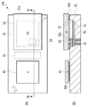
- FIG. 8 is a diagram showing the configuration of a conventional optoelectronic integrated module.
- FIG. 8A is a top view of the substrate surface
- FIG. 8B is a side view of a cross section of the substrate passing through the VIIIb-VIIIb line.
- an optical IC 10 PIC: Photonic Integrated Circuit
- an electric IC 20 for driving an optical circuit an electric IC 40 for signal processing such as a DSP are mounted on a substrate 30 via a solder ball or a gold bump 33.
- a solder ball 34 is provided on the lower surface side of the substrate 30 so that it can be mounted on the apparatus.
- an electric signal wiring area 22 although the wiring itself is not specified. Passing through the wiring region 22 may be, for example, an electric signal for transmission generated by performing signal processing with the electric IC 40 for signal processing. It can also be a received electrical signal from the photodetector (PD) of the optical IC 10.
- PD photodetector
- the electric IC 40 for signal processing such as a DSP and the electric IC 20 for driving an optical circuit be arranged in close proximity to each other. Since the module is required to be miniaturized and the electric signal processing speed is increased at the same time, it is also necessary to narrow the electric signal wiring region 22 and make the electric signal wiring as short as possible. On the other hand, if the electric IC 20 for driving an optical circuit is close to the electric IC 40 for signal processing, which is a large heat source, it becomes difficult to design heat dissipation of the electric IC 20.
- the present invention has been made in view of such a problem, and an object of the present invention is to provide an optoelectronic integrated module having a heat dissipation configuration suitable for small size and high integration.
- one embodiment of the present invention comprises a substrate, an optical integrated circuit (IC) mounted on the substrate via a plurality of connections, and the optical IC.
- a first electric IC mounted facing the connection surface and electrically connected to the optical IC via a plurality of connecting portions, and a second mounted on the substrate via the plurality of connecting portions.
- the first electric IC is housed in a recess formed inside a region corresponding to the optical IC when the substrate surface is viewed on the substrate, and the first electric IC is housed in the recess.
- the space between the bottom surface of the first electric IC and the opposite surface of the connection surface of the first electric IC is a photoelectron integrated module connected via a filler.
- Another embodiment of the present invention comprises the above-mentioned optoelectronic integration module, a first housing surface that holds the optoelectronic integration module and is thermally connected to the opposite surface of the connection surface of the second electric IC, and the above-mentioned. It is a device including a housing having a second housing surface that is thermally connected to the opposite surface of the connection surface of the substrate to the optical IC from the first electric IC via the filler.
- the heat dissipation path of the electric IC for signal processing having high power consumption and the heat dissipation path of the electric IC for driving the optical circuit are separated in the module.
- the electric IC for driving the optical circuit is mounted on the connection surface of the optical IC with the connection surfaces facing each other, and the electric IC for driving the optical circuit is partly on the connection surface side with the optical IC on the substrate. It is stored in the formed recess (cavity).
- a heat dissipation path for an electric IC for driving an optical circuit by thermally coupling the bottom of the recess (cavity) formed on the substrate surface and the non-connecting surface (upper surface) of the electric IC for driving the optical circuit. Is configured.
- connection surface of an IC or a substrate is a case where the IC or the substrate has a first surface and a second surface on the opposite side (back side) of the IC or the substrate, and another substrate or component is used by soldering or bumping.
- Etc. shall refer to the surface that is mechanically or electrically connected.
- the connection surface side of the chip is usually a circuit configuration surface in which an electronic circuit element, an optical circuit element, or the like is configured.
- FIG. 1 is a diagram showing a configuration of a first embodiment of the optoelectronic integrated module of the present disclosure.
- FIG. 1A is a top view of the substrate surface
- FIG. 1B is a side view of a cross section passing through the Ib-Ib line.
- the dimensions in the thickness direction of each substrate are shown in a substantially enlarged size compared to the lateral direction, and the relative relationship of the actual dimensions of each part is accurately reflected in the drawing.
- the size of each part is drawn differently from the actual size for the sake of clarity.
- the optical IC 10 (PIC) and the second electric IC 40 are connected to the substrate 30 via a plurality of connecting portions 33a and 33b.
- the plurality of connecting portions 33a and 33b include, but are not limited to, solder balls, gold bumps, and the like.
- the first electric IC 20 is not mounted on the substrate 30 as in the conventional technique shown in FIG. 8, but is mounted on the connection surface side of the optical IC 10 facing the optical IC 10. As shown by the dotted line region 20 in the top view of FIG. 1A, the first electric IC 20 is arranged on the connection surface side (rear surface) of the optical IC 10 with the optical IC 10 mounted on the substrate. Has been done.
- a space (cavity) of a recess 31 capable of accommodating the first electric IC 20 is formed in a part of the substrate 30 on the connection surface side with the optical IC 10 side.
- the recess 31 is a space having a bottom surface lowered from the surface of the substrate 30, and has a flat bottom surface formed deeper than the height of the first electric IC 20.
- the non-connecting surface (opposite surface of the connecting surface) of the first electric IC 20 is not in direct contact with the bottom of the recess 31.
- the recess is also referred to as a cavity 31 for the sake of simplicity.
- the cavity 31 corresponds to the dotted line region 31a inside the outer shape of the optical IC 10.
- the bottom of the cavity 31 is filled with a filler 50 so as to be in contact with the opposite surface (upper surface) of the connection surface of the first electric IC 20.
- the heat dissipation via 32 is formed in the substrate 30 directly below the bottom of the cavity 31 at a position substantially corresponding to the first electric IC 20.
- the cavity 31 is shown as a rectangular parallelepiped (plate-shaped) concave portion, but the cavity 31 is limited to this shape as will be described later in other embodiments. No. If the first electric IC 20 mounted facing the connection surface of the optical IC 10 is housed inside, and a plurality of connection portions 33a with the optical IC 10 can be arranged outside the cavity region 31a on the substrate 30, the cavity 31
- the shape can be changed in various ways.
- the second electric IC 40 in the optoelectronic integrated module 100 is an IC for high-speed signal processing, and can be, for example, a DSP having a very large calorific value.
- the second electric IC 40 may be a chip (die) obtained by cutting a semiconductor substrate on which an electronic element is formed, or may be a semiconductor chip mounted on another interposer, frame, or the like. Further, it may be in the form of a package in which the entire semiconductor chip is molded. As shown in FIG. 1 (b), the second electric IC 40 of the bare chip can be flip-mounted on the substrate 30 by using the connecting portion 33c such as a solder ball or a gold bump. Further, the second electric IC 40 may be mounted on the substrate 30 by another connection method depending on its form. Although the second electric IC 40 is shown as a single one in FIG. 1, two or more electric ICs 40 for signal processing may be provided on the substrate 30.
- the optical IC 10 is a semiconductor or other material substrate on which an electronic element, an optical element, or an optical circuit is configured, and may be a chip (die) obtained by cutting the substrate.
- the optical IC 10 may be formed on an InP or a silicon substrate. Depending on the function to be realized, it may be in the form of a module mounted on another board or package together with other optical components and electronic components.
- a silicon photonics chip or a quartz-based planar lightwave circuit (PLC: Planar Lightwave Circuit) chip can be used as the optical IC 10.
- the bare chip optical IC 10 may be flip-mounted on the substrate 30 by using a connection portion 33a such as a solder ball or a gold bump, or the substrate 30 may be mounted by another method. May be mounted on.
- the substrate 30 is electrically connected to the substrate 30 by using the connecting portion 33a at the peripheral portion near the outer shell of the optical IC 10.
- the cavity 31 is formed in a region 31a inside the region where the connecting portion 33a is located in the optical IC 10, and further, inside the region 31a of the cavity, the first electric IC 20 described below is connected to the optical IC 10.
- the first electric IC 20 is integrated with a driving electronic device for supplying an electric signal to, for example, a modulator in the optical IC 10.
- the first electric IC 20 may be a chip (die) obtained by cutting a semiconductor substrate on which an electronic device is configured, or may be a semiconductor chip mounted on another interposer, frame, or the like. Further, it may be in the form of a package in which the entire semiconductor chip is molded.
- the electric signal wiring region 22 is a region through which the wiring of the high frequency electric signal from the second electric IC 40 passes, and is configured as a transmission line having a predetermined characteristic impedance so that loss or reflection does not occur in the high frequency signal. ..
- a ceramic or organic material substrate can be used so as to have sufficient strength and thermal conductivity and to prevent loss of high frequency signals.
- a chip capacitor and other integrated electronic components can be mounted on the electrical signal wiring region 22.
- the optical electron integrated module of the present disclosure faces the substrate 30, the optical integrated circuit (IC) 10 mounted on the substrate via a plurality of connecting portions 33a, and the connecting surface of the optical IC.
- a first electric IC 20 mounted and electrically connected to the optical IC via a plurality of connecting portions 33c, and a second electric IC 40 mounted on the substrate via the plurality of connecting portions 33b.
- the first electric IC is housed in a recess 31 formed inside a region 31a corresponding to the optical IC when the substrate surface is viewed on the substrate, and the bottom surface of the recess is provided. And between the opposite surfaces of the connection surface of the first electric IC, it can be carried out as if they are connected via the filler 50.
- the first electric IC 20 for example, amplifies an electric signal for modulation from a DSP to a current / voltage level required for operating an optical modulator (Machzenda modulator, EA modulator, etc.). Including the function to supply. Taking an optical transmitter / receiver as an example, the number of electric signals varies depending on the modulation method, the number of multiplexings, the signal transmission type (single-ended, differential), etc., but generally, at most several tens of electric signals are driven. Normally, the first electric IC 20 is smaller than the second electric IC 40 such as a DSP that performs signal processing at high speed, and the amount of heat generated is relatively small.
- the second electric IC 40 such as a DSP that performs signal processing at high speed, and the amount of heat generated is relatively small.
- the function of the first electric IC 20 may include amplifying the electric signal from the PD in the optical IC 10 and supplying it to the second electric IC 40. Therefore, the first electric IC can also be an electric IC for an interface with an optical circuit. In FIG. 1, the first electric IC 20 is shown as a single one, but two or more electric ICs for driving an optical circuit may be provided.
- the configuration of the optoelectronic integrated module of the present disclosure is different from the second electric IC 40 for high-speed signal processing in terms of device type, operating voltage / current range, and function. Therefore, the electric IC is separate from the second electric IC 40. Can be widely applied to devices equipped with. It should be noted that the function of the first electric IC 20 is not limited to driving an optical circuit.
- an electric IC 20 for driving an optical circuit is arranged between the electric signal wiring region 22 on the substrate 30 and the optical IC 10, and the light is optical via the first electric IC 20.
- the electric signal after driving was input to IC10.
- the first electric IC 20 for driving the optical circuit is not arranged on the substrate 30. Therefore, the electric signal from the electric signal wiring area 22 is first input to the optical IC 10 via the connection portion 33a near the wiring area 22.
- the electric signal input to the optical IC 10 is input to the first electric IC 20 via a part of the connection portion 33c.
- the electric signal is driven to a predetermined level by the electronic device in the first electric IC 20, and then again supplied to the optical IC 10 via the other connection 33c.
- the optical IC 10 and the first electric IC 20 are electrically connected with their connection surfaces facing each other. Since the optical IC 10 is mounted on the substrate 30 as in the prior art, the first electric IC 20 is mounted on the connection surface of the optical IC 10, that is, the lower surface in the mounted state by inverting (turning over) the upper and lower surfaces. .. In the case of the first electric IC 20 using the bare chip of FIG. 1 (b), it is flip-mounted on the optical IC 10 of the bare chip by a connecting portion 33c such as a solder ball or a gold bump. In the case of the configuration of (b) of FIG.
- the circuit forming surfaces of the two chips face each other.
- the method of mounting the first electric IC 20 on the optical IC 10 is not limited to flip mounting, and the first electric IC 20 can be mounted on the connection surface of the optical IC 10 by wire bonding.
- the optical IC 10 in which the first electric IC 20 is mounted by wire bonding can be mounted on the substrate 30 and flip-mounted.
- the optical IC 10 and the first electric IC 20 are mounted on the connection surface side of the optical IC 10 and are electrically connected with the connection surfaces facing each other, and at the same time, the first electric IC 20 is not.
- a new heat dissipation path can be created between the connection surface and the bottom surface of the cavity 31.
- the non-connecting surface where the first electric IC 20 does not face the optical IC 10 is thermally connected to the heat dissipation via 32 by coming into contact with the filler 50 filled in the bottom of the cavity 31.
- the first electric IC 20 By connecting the first electric IC 20 to the heat radiating via 32 via the filler 50, it can be thermally connected to the housing on which the substrate 30 is mounted, another substrate of the device, or the like by the heat radiating mechanism.
- the connection with other heat dissipation mechanisms will be described later in the sixth and seventh embodiments.
- the heat dissipation path through the non-connecting surface of the first electric IC 20 is reversed with respect to the substrate 30 by reversing the front and back of the connecting surface of the first electric IC 20 for driving the optical circuit. It is newly established.
- the first electric IC 20 and the second electric IC 40 use a heat dissipation path that is generally common, only the amount of heat determined by the thermal resistance of the substrate 30 can be transferred. ..
- the optical electron integrated module 100 of the present disclosure by providing a new heat dissipation path dedicated to the first electric IC 20 using the cavity, the external is irrespective of the heat dissipation status of the second electric IC 40 for signal processing having a large heat generation amount. It is possible to efficiently dissipate heat to the device side of. By providing a new heat dissipation path in parallel for the entire optoelectronic integrated module, the overall thermal resistance can be reduced.
- the thermal influence on the first electric IC 20 changes with time depending on the driving state of the second electric IC 40 (for example, on / off of the function), and the driving state of the first electric IC 20 is changed. Is also concerned about the impact.
- the heat dissipation paths are separately and independently provided for the two electric ICs, and the heat dissipation paths are different. Therefore, it is possible to suppress fluctuations in the thermal influence between the electric ICs, for example, having a different influence on the driving operation of the optical circuit depending on the operating state of the DSP. Further improvement can be expected in the operational stability of the optoelectronic integrated module.
- the first electric IC 20 When the first electric IC 20 is for driving an optical circuit, it can be expected to stabilize the operation and improve the reliability of the optoelectronic integrated module by lowering the junction temperature of the amplification element inside the first electric IC 20.
- the second electric IC 40 since the second electric IC 40 can be brought closer to the optical IC 10 than in the prior art, it is suitable for expanding the high frequency band characteristic of the electric signal while reducing the heat dissipation problem.
- an underfill or an adhesive having good heat dissipation can be used as the filler 50.
- Any material may be used as long as it is a material having excellent thermal conductivity and functions as a spacer for the first electric IC 20 in the cavity 31.
- an acrylic-based elastic adhesive or a heat-dissipating paste can be used as a material for the underfill and the adhesive.
- both ICs are in the form of bare chips, and an example of flip-connecting mutual connections is shown, but at least the second electric IC 40 may be in the form of a module.
- the optical IC 10 may be provided with a structure that further enhances heat dissipation efficiency, such as being provided with a penetrating via.
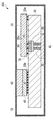
- FIG. 2 is a diagram showing a configuration of a second embodiment of the optoelectronic integrated module of the present disclosure.
- FIG. 2A is a top view of the substrate surface
- FIG. 2B is a side view of a cross section passing through the IIb-IIb line
- FIG. 2C is a side view of a cross section passing through the IIc-IIc line. It is a side view.
- the photoelectron integration module 200 differs from the first embodiment only in the configuration of the recess formed on the substrate 30 for accommodating the first electric IC 20, that is, the cavity 31, and the basic configuration is the optoelectronic integration module 100 of FIG. It is the same. Therefore, the differences in the configurations of the cavities 31 will be described below.
- the cavity 31 is covered with the entire optical IC 10 in the state after the optical IC 10 is mounted. Therefore, it is necessary to inject the filler 50 into the cavity before mounting the optical IC 10.
- the optoelectronic integrated module 200 is formed so as to extend continuously from at least one inner side surface of the cavity 31 toward the side portion of the substrate 30 and open to the substrate surface outside the region of the optical IC 10.
- An injection port which is an opening, is provided. Specifically, as shown in FIG. 2A, two openings 31b, 31c extending from the two inner side surfaces toward the end of the substrate 30 in the cavity region 31a and opening on the upper surface of the substrate. It is equipped with.
- the filler 50 can be injected through the openings 31b and 31c, so that the filler 50 can be injected even after the optical IC 10 is mounted on the substrate 30.
- the first optical IC 10 has a filler near the connection portion of the substrate 30, there is a concern that the flip chip conditions may change depending on the filling state of the filler in the flip chip step of the first optical IC 10.
- even a material that cannot withstand the temperature of the flip chip mounting process of the optical IC 10 can be used as a filler. Flexibility can be increased in the material selection of the filler 50.
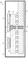
- FIG. 3 is a diagram showing a configuration of a third embodiment of the optoelectronic integrated module of the present disclosure.
- FIG. 3A is a top view of the substrate surface
- FIG. 3B is a side view of a cross section passing through the line IIIb-IIIb.
- the photoelectron integration module 300 of the third embodiment is obtained by further modifying the configuration of the bottom surface of the cavity 31 with respect to the configuration of the optoelectronic integration module 200 shown in FIG. 2, and this change will be described.
- the photoelectron integration module 300 has a bottom surface formed one step deeper in the region near the first electric IC 20 inside the region 31a of the cavity.
- a second cavity 31d is provided.
- the second cavity 31d has a second bottom surface formed deeper in the substrate thickness direction. The second bottom surface is provided at a position deeper than the bottom surface of the cavity 31, and the filler 50 is arranged only inside the second cavity 31d.
- the filler 50 Due to the difference in bottom depth between the two cavities 31 and 31d, even when the filler 50 is injected after the optical IC 10 is mounted on the substrate 30, the filler is injected only directly under the first electric IC 20. can.
- the filler 50 is not required as a heat dissipation path in a place away from the place where the first electric IC 20 and the filler 50 come into contact with each other. If the filler is inadvertently introduced in a place that does not contribute to heat dissipation, problems such as void generation may occur in the filler.
- the filler 50 can be localized only in the second cavity 31d where the filler is required, and the filler 50 can be introduced in a necessary and sufficient amount. It is possible to save waste of the filler and reduce the possibility of defects caused by the filler.
- FIG. 4 is a diagram showing a configuration of a fourth embodiment of the optoelectronic integrated module of the present disclosure.
- FIG. 4A is a top view of the substrate surface
- FIG. 4B is a side view of a cross section passing through the VIb-VIb line.
- the optoelectronic integration module 400 differs from the third embodiment only in the configuration of the cavity 31, and the basic configuration is the same as that of the optoelectronic integration module 300 of FIG. Therefore, the differences in the configuration of the cavity 31 will be described below.
- the optoelectronic integrated module 400 has a narrow region 31a limited to a region near the first electric IC 20 as compared with the previous embodiments. Is provided with a cavity 31 and openings 31b, 31c. Therefore, the configuration of this embodiment corresponds to the photoelectron integration module 200 of the second embodiment in which the region of the cavity 31 having a one-stage bottom surface is made as small as possible. Further, the configuration of the present embodiment can be seen as the photoelectron integration module 300 of the third embodiment in which the height of the bottom of the cavity 31 is raised to the uppermost surface of the substrate 30.
- the photoelectron integration module 400 of the present embodiment simplifies the injection of the filler from the openings 31b and 31c, and maintains the heat dissipation path from the first electric IC 20 while maintaining the minimum required filler in the cavity 31. 50 can be inserted.
- FIG. 5 is a diagram showing a configuration of a fifth embodiment of the optoelectronic integrated module of the present disclosure.
- FIG. 5A is a top view of the substrate surface
- FIG. 5B is a side view of a cross section passing through the Vb—Vb line.
- the optoelectronic integrated module 500 differs from the above-described embodiment in the shape of the cavity 31 and the configuration between the connection surface of the optical IC 10 and the substrate 30, and the basic configuration as the optoelectronic integrated module is the first to fourth embodiments. Common to the form.
- the cavity region 31a is reduced to the time of the first electric IC 20, and the cavity of the optoelectronic integration module 100 of FIG. 1 is formed.
- the region 31a of is made as small as possible.
- the opening for injecting the filler is not provided.
- the filler 51 is also filled between the connection surface of the first electric IC 20 and the substrate 30. This can be carried out as an underfill coating step for protecting the connection portion 33 when the first electric IC 20 is flip-chip connected.
- the injection of the filler 50 between the first electric IC 20 and the bottom of the cavity 31 can be performed simultaneously as one step.
- the filler 50 is localized in the cavity 31 having the smallest area, and the filler 50 is filled in the entire cavity 31 by simplifying the control of the coating amount of the filler. Is also good.
- connection form and the heat dissipation path of the main ICs constituting the optoelectronic integrated module have been described, but in order to mount the optoelectronic integrated module in a higher-level device, it is necessary to further house it in a housing. be.
- the heat dissipation mechanism including the housing will be described.
- FIG. 6 is a diagram showing a configuration of a sixth embodiment of the optoelectronic integrated module of the present disclosure.
- the optoelectronic integration module 600 of FIG. 6 includes a housing 72 for accommodating the whole, in addition to the components of the optoelectronic integration module so far.
- the configuration of the first electric IC 10 and the cavity mounted on the substrate 30 corresponds to the photoelectron integration module 300 of the third embodiment shown in FIG. Therefore, the heat dissipation configuration between the housing 72 and the optoelectronic integrated module 300 will be described below.
- the second electric IC 40 mounted on the substrate 30 is thermally connected to the first surface of the housing 72 (the upper housing surface in FIG. 6) via the heat transfer material 62.
- the first electric IC 20 is thermally connected to the second surface (lower housing surface of FIG. 6) of the housing 72 via the filler 50, the heat radiating via 32, and the heat transfer material 61.
- the exhaust heat from the second electric IC 40 and the exhaust heat from the first electric IC 20 are performed toward different surfaces of the housing 72, respectively.
- the heat transfer materials 61 and 62 for example, a heat radiating sheet or a heat radiating paste can be used.
- the optoelectronic integrated module 600 of this embodiment corresponds to a very compact device that houses a substrate 30 on which an optical IC and at least two types of electric ICs are mounted.
- a CFP, QSFP type optical transmitter / receiver as shown in Non-Patent Document 1.
- FIG. 7 is a diagram showing a configuration of a seventh embodiment of the optoelectronic integrated module of the present disclosure.
- the optoelectronic integrated module 700 of the present embodiment shows a configuration example in which the substrate 30 of each of the above-described embodiments is housed in the housing 72 in a state of being further mounted on another substrate 60. Therefore, a heat dissipation mechanism in which a photoelectron integrated module having a new heat dissipation path of an electric IC via a cavity formed on the substrate 30 described above is mounted on a higher-level device will be described. Therefore, it may be the optoelectronic integration module of FIG. 7 or another device including the optoelectronic integration module.
- the second electric IC 40 is thermally connected to the first surface of the housing 72 (the upper housing surface of FIG. 6) via the heat transfer material 62.
- the entire substrate 30 of the optoelectronic integration module is mounted on another larger second substrate 60 of the device via the solder balls 34.
- a heat radiating via 63 is also provided on the other substrate 60, and the heat radiating vias 32 of the substrate 30 to the heat radiating vias 63 of the second substrate 60 are provided via the solder balls 34.
- the second substrate 60 is thermally connected to the second surface (lower housing surface of FIG. 6) of the housing 72 via the heat transfer material 61.
- heat is radiated from the second electric IC 40 to the upper surface of the housing 72 and from the first electric IC 20 to the lower surface of the housing 72 via the heat transfer material 61 of another substrate 60.
- the route can be separated.
- the heat radiating via 63 and the heat radiating via 32 are thermally connected by the solder balls 34, but they may be connected by another heat conductive member.
- the first electric IC and the second electric IC are different types of electric ICs in their functions and calorific value. Since the second electric IC 40 has a larger calorific value, it is mounted directly on the substrate 30. On the other hand, since the first electric IC 20 has a relatively small calorific value, it is mounted on the optical IC with the connection surfaces facing each other, but it is sufficient for improving the performance and reliability of the electronic devices contained therein. Great heat dissipation is required.
- the second electrical IC 40 may be a DSP for high speed signal processing and the first electrical IC 20 may include a driver circuit for driving an optical circuit.
- both the first electric IC 120 and the second electric IC 40 are shown as a single one, but each of them may be composed of two or more ICs.
- the first electric IC 20 and optical IC 10 may have various mounting forms such as a bare chip form, a chip mounted on another interposer, a frame, or a module form.
- the optoelectronic integrated module of the present disclosure at least one of the electric ICs is connected to the optical IC with the connection surfaces facing each other, and the electric IC having the upper and lower surfaces inverted is formed on the substrate.
- the electric IC having the upper and lower surfaces inverted is formed on the substrate.
- the present invention can generally be used for an optical communication system.
Landscapes
- Physics & Mathematics (AREA)
- General Physics & Mathematics (AREA)
- Optics & Photonics (AREA)
- Optical Couplings Of Light Guides (AREA)
Priority Applications (3)
| Application Number | Priority Date | Filing Date | Title |
|---|---|---|---|
| JP2022528369A JP7372576B2 (ja) | 2020-06-05 | 2020-06-05 | 光電子集積モジュール |
| US18/007,635 US12332489B2 (en) | 2020-06-05 | 2020-06-05 | Opto-electronic integrated module |
| PCT/JP2020/022253 WO2021245907A1 (ja) | 2020-06-05 | 2020-06-05 | 光電子集積モジュール |
Applications Claiming Priority (1)
| Application Number | Priority Date | Filing Date | Title |
|---|---|---|---|
| PCT/JP2020/022253 WO2021245907A1 (ja) | 2020-06-05 | 2020-06-05 | 光電子集積モジュール |
Publications (1)
| Publication Number | Publication Date |
|---|---|
| WO2021245907A1 true WO2021245907A1 (ja) | 2021-12-09 |
Family
ID=78830744
Family Applications (1)
| Application Number | Title | Priority Date | Filing Date |
|---|---|---|---|
| PCT/JP2020/022253 Ceased WO2021245907A1 (ja) | 2020-06-05 | 2020-06-05 | 光電子集積モジュール |
Country Status (3)
| Country | Link |
|---|---|
| US (1) | US12332489B2 (https=) |
| JP (1) | JP7372576B2 (https=) |
| WO (1) | WO2021245907A1 (https=) |
Families Citing this family (2)
| Publication number | Priority date | Publication date | Assignee | Title |
|---|---|---|---|---|
| CN114899182B (zh) * | 2022-04-25 | 2026-01-23 | 深圳市思坦科技有限公司 | 微型led器件的封装结构及方法以及显示装置 |
| CN116344629B (zh) * | 2023-02-24 | 2025-09-30 | 深南电路股份有限公司 | 一种基于玻璃波导的光电混合器件及其制作方法 |
Citations (5)
| Publication number | Priority date | Publication date | Assignee | Title |
|---|---|---|---|---|
| JP2006073651A (ja) * | 2004-08-31 | 2006-03-16 | Fujitsu Ltd | 半導体装置 |
| JP2009164564A (ja) * | 2007-12-14 | 2009-07-23 | Denso Corp | 電子装置およびその製造方法 |
| JP2012114334A (ja) * | 2010-11-26 | 2012-06-14 | Nec Casio Mobile Communications Ltd | キャビティ基板を備える半導体モジュール、その不良解析方法、及び該半導体モジュールの製造方法 |
| WO2014020787A1 (ja) * | 2012-08-03 | 2014-02-06 | パナソニック株式会社 | 電子部品モジュールとその実装体 |
| JP2015029043A (ja) * | 2013-06-26 | 2015-02-12 | 京セラ株式会社 | 電子装置および光モジュール |
Family Cites Families (2)
| Publication number | Priority date | Publication date | Assignee | Title |
|---|---|---|---|---|
| US8111730B2 (en) * | 2009-08-20 | 2012-02-07 | International Business Machines Corporation | 3D optoelectronic packaging |
| US9543226B1 (en) * | 2015-10-07 | 2017-01-10 | Coriant Advanced Technology, LLC | Heat sink for a semiconductor chip device |
-
2020
- 2020-06-05 WO PCT/JP2020/022253 patent/WO2021245907A1/ja not_active Ceased
- 2020-06-05 JP JP2022528369A patent/JP7372576B2/ja active Active
- 2020-06-05 US US18/007,635 patent/US12332489B2/en active Active
Patent Citations (5)
| Publication number | Priority date | Publication date | Assignee | Title |
|---|---|---|---|---|
| JP2006073651A (ja) * | 2004-08-31 | 2006-03-16 | Fujitsu Ltd | 半導体装置 |
| JP2009164564A (ja) * | 2007-12-14 | 2009-07-23 | Denso Corp | 電子装置およびその製造方法 |
| JP2012114334A (ja) * | 2010-11-26 | 2012-06-14 | Nec Casio Mobile Communications Ltd | キャビティ基板を備える半導体モジュール、その不良解析方法、及び該半導体モジュールの製造方法 |
| WO2014020787A1 (ja) * | 2012-08-03 | 2014-02-06 | パナソニック株式会社 | 電子部品モジュールとその実装体 |
| JP2015029043A (ja) * | 2013-06-26 | 2015-02-12 | 京セラ株式会社 | 電子装置および光モジュール |
Also Published As
| Publication number | Publication date |
|---|---|
| JP7372576B2 (ja) | 2023-11-01 |
| JPWO2021245907A1 (https=) | 2021-12-09 |
| US12332489B2 (en) | 2025-06-17 |
| US20230244045A1 (en) | 2023-08-03 |
Similar Documents
| Publication | Publication Date | Title |
|---|---|---|
| JP4131935B2 (ja) | インターフェイスモジュールとインターフェイスモジュール付lsiパッケージ及びその実装方法 | |
| JP3728147B2 (ja) | 光電気混載配線基板 | |
| CN106664139B (zh) | 多通道相干收发器及相关装置和方法 | |
| CN214795314U (zh) | 一种光模块 | |
| CN214795313U (zh) | 一种光模块 | |
| CN101911405B (zh) | 光模块 | |
| JP2005182033A (ja) | 光相互接続モジュール用のシリコン・キャリア | |
| US20180019569A1 (en) | Optical transmitter with a heat dissipation structure | |
| US12468102B2 (en) | Optical module | |
| CN106980159A (zh) | 基于光电混合集成的光电模块封装结构 | |
| US12422634B2 (en) | Optical module package structure | |
| US7217043B2 (en) | Optoelectronic transceiver | |
| CN113759472B (zh) | 一种光模块 | |
| US20230116287A1 (en) | Optical module | |
| CN113009649B (zh) | 一种光模块 | |
| JP3684112B2 (ja) | 光電気混載配線基板、その駆動方法、およびそれを用いた電子回路装置 | |
| US20240302611A1 (en) | Photoelectric transceiver assembly and manufacturing method thereof | |
| WO2021245907A1 (ja) | 光電子集積モジュール | |
| JP2012145743A (ja) | 光モジュール | |
| CN113659441A (zh) | 一种激光器组件及光模块 | |
| CN113325526A (zh) | 一种光模块 | |
| JP2020060734A (ja) | 光モジュール | |
| CN120762169A (zh) | 一种光模块 | |
| US20060024067A1 (en) | Optical I/O chip for use with distinct electronic chip | |
| WO2022262551A1 (zh) | 一种光模块 |
Legal Events
| Date | Code | Title | Description |
|---|---|---|---|
| 121 | Ep: the epo has been informed by wipo that ep was designated in this application |
Ref document number: 20938995 Country of ref document: EP Kind code of ref document: A1 |
|
| ENP | Entry into the national phase |
Ref document number: 2022528369 Country of ref document: JP Kind code of ref document: A |
|
| NENP | Non-entry into the national phase |
Ref country code: DE |
|
| 122 | Ep: pct application non-entry in european phase |
Ref document number: 20938995 Country of ref document: EP Kind code of ref document: A1 |
|
| WWG | Wipo information: grant in national office |
Ref document number: 18007635 Country of ref document: US |