WO2021241053A1 - 固体撮像装置および電子機器 - Google Patents
固体撮像装置および電子機器 Download PDFInfo
- Publication number
- WO2021241053A1 WO2021241053A1 PCT/JP2021/015528 JP2021015528W WO2021241053A1 WO 2021241053 A1 WO2021241053 A1 WO 2021241053A1 JP 2021015528 W JP2021015528 W JP 2021015528W WO 2021241053 A1 WO2021241053 A1 WO 2021241053A1
- Authority
- WO
- WIPO (PCT)
- Prior art keywords
- substrate
- image sensor
- solid
- state image
- connector
- Prior art date
- Legal status (The legal status is an assumption and is not a legal conclusion. Google has not performed a legal analysis and makes no representation as to the accuracy of the status listed.)
- Ceased
Links
Images









Classifications
-
- H—ELECTRICITY
- H04—ELECTRIC COMMUNICATION TECHNIQUE
- H04N—PICTORIAL COMMUNICATION, e.g. TELEVISION
- H04N23/00—Cameras or camera modules comprising electronic image sensors; Control thereof
- H04N23/50—Constructional details
- H04N23/54—Mounting of pick-up tubes, electronic image sensors, deviation or focusing coils
-
- H—ELECTRICITY
- H10—SEMICONDUCTOR DEVICES; ELECTRIC SOLID-STATE DEVICES NOT OTHERWISE PROVIDED FOR
- H10F—INORGANIC SEMICONDUCTOR DEVICES SENSITIVE TO INFRARED RADIATION, LIGHT, ELECTROMAGNETIC RADIATION OF SHORTER WAVELENGTH OR CORPUSCULAR RADIATION
- H10F39/00—Integrated devices, or assemblies of multiple devices, comprising at least one element covered by group H10F30/00, e.g. radiation detectors comprising photodiode arrays
- H10F39/80—Constructional details of image sensors
-
- H—ELECTRICITY
- H10—SEMICONDUCTOR DEVICES; ELECTRIC SOLID-STATE DEVICES NOT OTHERWISE PROVIDED FOR
- H10F—INORGANIC SEMICONDUCTOR DEVICES SENSITIVE TO INFRARED RADIATION, LIGHT, ELECTROMAGNETIC RADIATION OF SHORTER WAVELENGTH OR CORPUSCULAR RADIATION
- H10F39/00—Integrated devices, or assemblies of multiple devices, comprising at least one element covered by group H10F30/00, e.g. radiation detectors comprising photodiode arrays
- H10F39/80—Constructional details of image sensors
- H10F39/804—Containers or encapsulations
Definitions
- This technology relates to solid-state image sensors and electronic devices.
- the image sensor is mounted on a substrate made of a material such as an organic material or ceramics, and a translucent member such as glass is provided on the light receiving surface side of the image sensor so as to form a hollow portion together with a predetermined support member. It is a provided package structure.
- An image sensor is a chip in which a plurality of light receiving elements constituting pixels are formed on one plate surface side of a semiconductor substrate such as silicon (Si), and is directly on the substrate with an adhesive or via a metal plate or the like. It is indirectly mounted via the mounting member.
- an image sensor is mounted on a housing as a support member for supporting glass, and electrode terminals such as leads and pins are extended on the back side of the housing to form a housing.
- a configuration is disclosed in which a space is secured between the substrate and the space and a metal plate is interposed in the space.
- a method is adopted in which a metal plate is brought into contact with the lens housing covering the package structure and heat is dissipated by providing a heat conductive member in the housing.
- Patent Document 1 As disclosed in Patent Document 1, according to the configuration in which electrode terminals such as pins are extended on the back side of the housing and a metal plate is interposed between the housing and the substrate, a high-speed interface is supported. In the case of a multi-pin image sensor, it is difficult to narrow the distance between electrode terminals such as pins, and the package size becomes large. Further, when the package size becomes large, the wiring length becomes long due to the influence, and there is a problem that the transmission delay of the high-speed interface occurs.
- Patent Document 2 According to the configuration in which the holding metal fitting of the image sensor or the metal fitting for heat dissipation is brought into contact with the image sensor by penetrating the holding metal fitting or the substrate, the heat dissipation of the image sensor is suppressed while suppressing the package size. Is thought to be possible. However, according to the configuration disclosed in Patent Document 2, there is a problem that the shape of each component becomes complicated, the number of components increases, and the time and effort required for mounting the components increases.
- An object of the present technology is to provide a solid-state image sensor and an electronic device capable of reducing the package size and suppressing the transmission delay of a high-speed interface by a simple structure in dealing with heat generation of a solid-state image sensor. It is to be.
- the solid-state image sensor includes a solid-state image sensor whose light receiving side is one plate surface side of a semiconductor substrate, a substrate on which the solid-state image sensor is mounted on the surface of one plate surface, and the above-mentioned substrate.
- a support member provided on the front surface side so as to surround the solid-state image sensor, and a plurality of connectors provided on the back surface of the other plate surface of the substrate and located outside the arrangement region of the solid-state image sensor on the substrate.
- the connector is such that at least a part thereof is located outside the arrangement area of the support member in the substrate.
- the substrate is fitted on the outside of the arrangement region of the support member on the surface side, and the connector is fitted in a fitted portion with respect to the connector. It has a pressed portion that receives a load for matching.
- Another aspect of the solid-state image pickup device according to the present technology is that in the solid-state image pickup device, at least one of the substrate and the support member is outside the arrangement region of the solid-state image pickup device in the plate thickness direction of the substrate.
- a hole is formed so as to be used for at least one of the positioning of the mounted components on the substrate and the attachment of the substrate to an external device.
- a recess is formed on the back surface side of the substrate so that at least a part of the solid-state image pickup device is located in the arrangement region of the solid-state image sensor. Is what you are doing.
- Another aspect of the solid-state image pickup device is that in the solid-state image pickup device, a step portion corresponding to the height of the plurality of connectors is formed on the back surface side of the substrate.
- the electronic device includes a solid-state image sensor whose light receiving side is one plate surface side of a semiconductor substrate, a substrate on which the solid-state image sensor is mounted on the surface of one plate surface, and the surface of the substrate.
- a support member provided on the side so as to surround the solid-state image sensor, and a plurality of connectors provided on the back surface of the other plate surface of the substrate and located outside the arrangement region of the solid-state image sensor on the substrate.
- the connector is provided with a solid-state image sensor that positions at least a part of the substrate outside the area of placement of the support member on the substrate.
- This technology makes it possible to dissipate heat from the solid-state image sensor with a simple configuration by devising the layout of the frame, connector, etc. on the board on which the solid-state image sensor is mounted, and suppresses the increase in package size. And it is intended to suppress the transmission delay of the high-speed interface.
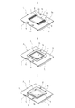
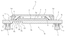
- the solid-state image sensor 1 includes an image sensor 2 as a solid-state image sensor, a substrate 3 on which the image sensor 2 is mounted, and a frame 4 as a support member provided on the substrate 3. And a plurality of connectors 5 for electrically connecting the solid-state image pickup device 1 to the external device. Further, the solid-state image sensor 1 includes glass 6 as a translucent member supported on the frame 4.
- the solid-state image sensor 1 has a package structure in which a glass 6 is mounted on a substrate 3 via a frame 4 and a cavity 7 as a hollow portion is provided between the image sensor 2 and the glass 6. That is, the glass 6 is provided above the image sensor 2 so as to face the image sensor 2, and the cavity 7 which is a closed space formed by the frame 4 and the glass 6 is formed on the substrate 3.
- a plurality of connectors 5 are provided on the side of the substrate 3 opposite to the image sensor 2 side.
- the solid-state image sensor 1 is configured as an image sensor connector package.
- the image sensor 2 includes a silicon semiconductor substrate made of silicon (Si), which is an example of a semiconductor, and one plate surface side (upper side in FIG. 1) of the semiconductor substrate is the light receiving side.
- the image sensor 2 is a rectangular plate-shaped chip, and the plate surface on the light receiving side is the front surface 2a, and the plate surface on the opposite side is the back surface 2b.
- the image sensor 2 is made of a die bond material or the like, and is mounted in the central portion on the substrate 3 with the back surface 2b side as the substrate 3 side.
- the image sensor 2 according to the present embodiment is a CMOS (Complementary Metal Oxide Semiconductor) type image sensor.
- the image sensor 2 may be a CCD (Charge Coupled Device) type image sensor.
- the image sensor 2 is composed of a semiconductor substrate, and an image sensor element is formed on the surface 2a side.
- the image sensor 2 has a pixel region 2c on the surface 2a side, which is a light receiving region including a large number of pixels formed in a predetermined arrangement such as a Bayer array, as a light receiving portion, and is around the pixel region 2c. Let the area of be the peripheral area.
- the pixel region 2c includes an effective pixel region that generates, amplifies, and reads a signal charge by photoelectric conversion in each pixel.
- the pixel in the pixel region 2c has a photodiode as a photoelectric conversion unit having a photoelectric conversion function, and a plurality of pixel transistors.
- a color filter and an on-chip lens are attached to each pixel of the semiconductor substrate via an antireflection film made of an oxide film or the like, a flattening film made of an organic material, or the like. Correspondingly formed.
- the light incident on the on-chip lens is received by the photodiode through a color filter, a flattening film, or the like.
- a surface illumination type (Front Side Illumination) in which a pixel region 2c is formed on the surface side of a semiconductor substrate, a photodiode or the like is arranged in reverse in order to improve the light transmission rate.
- a back-illuminated type (Back Side Illumination) in which the back surface side of the semiconductor substrate is the light receiving surface side, and a single chip in which peripheral circuits of a pixel group are laminated.
- the image sensor 2 according to the present technology is not limited to those having these configurations.
- the substrate 3 has a rectangular plate-like outer shape as a whole, and has a front surface 3a which is one plate surface on which the image sensor 2 is mounted and a back surface 3b which is the other plate surface on the opposite side.
- the substrate 3 constitutes a portion of the solid-state image sensor 1 in which the image sensor 2 is mounted on the surface 3a.
- the longitudinal direction (horizontal direction in FIG. 1) of the rectangular plate-shaped substrate 3 is the left-right direction
- the direction orthogonal to the left-right direction in the plan view is the front-back direction
- the plate of the substrate 3 is
- the thickness direction (vertical direction in FIG. 1) is defined as the vertical direction.
- the substrate 3 is, for example, a base material formed of an organic material such as plastic or a material such as ceramics provided with a wiring layer, electrodes and the like.
- the substrate 3 according to the present embodiment is, for example, a ceramic substrate containing aluminum oxide as a main component.
- the image sensor 2 and the substrate 3 are electrically connected by a bonding wire 8 as a connecting member.
- the bonding wire 8 is provided so as to straddle between the surface 2a of the image sensor 2 and the surface 3a of the substrate 3 while forming an upwardly convex curved or bent shape such as an arch shape.
- the bonding wire 8 is a thin metal wire made of, for example, Au (gold) or Cu (copper).
- the bonding wire 8 electrically connects an electrode (not shown) formed on the surface 2a of the image sensor 2 and a pad electrode 9 formed on the surface 3a of the substrate 3.
- a plurality of bonding wires 8 are provided according to the number of pad electrodes 9.
- the pad electrode 9 is made of, for example, an aluminum material.
- the frame 4 is provided on the surface 3a side of the substrate 3 so as to surround the image sensor 2.
- the frame 4 is an integral member made of a resin material or a metal material.
- the frame 4 may have a composite structure having a portion made of a metal material and a portion made of a resin material.
- the frame 4 is a rectangular or square frame-shaped member, and has an outer dimension larger than the plan view outer shape of the image sensor 2 and smaller than the plan view outer shape of the substrate 3.
- the frame 4 has four linear side portions 4a having a frame-like shape, and the four side portions 4a form a rectangular opening 4b.
- the dimension of the plan view outer shape of the opening 4b is larger than the plan view outer shape of the image sensor 2.
- the frame 4 is provided so as to surround the image sensor 2 along the outer shape of the rectangular image sensor 2.
- Each frame 4 has an upper surface 4c and a lower surface 4d along a horizontal plane.
- the outer side surface 4e is a surface along the vertical direction.
- the upper portion of the inner surface forming the opening 4b is an inclined surface portion 4f inclined from the lower side to the upper side in a side sectional view (cross-sectional view) from the outer side to the inner side.
- the lower portion of the inclined surface portion 4f is a lower side surface portion 4g along the vertical direction.
- the cavity 7 Due to the shape of the inner surface of the frame 4, the cavity 7 has a wider lower space than the upper space, and the opening area on the upper surface 4c side of the opening 4b is the opening on the lower surface 4d side of the opening 4b. It is smaller than the area.
- the shape of the inner surface of the frame 4 is not limited to this embodiment. Further, although the frame 4 is a frame-shaped integrated member, it may be a portion composed of a plurality of members forming a part of the rectangular frame shape.
- the frame 4 is provided on the surface 3a of the substrate 3 so that the entire pixel region 2c is located within the opening range of the opening 4b in a plan view with respect to the image sensor 2 mounted on the substrate 3. Further, the frame 4 is provided without interfering with the bonding wire 8 and the pad electrode 9.
- the frame 4 is fixed on the surface 3a of the substrate 3 with an adhesive such as an epoxy resin adhesive or an acrylic resin adhesive.
- the upper surface 4c is a surface that supports the glass 6.
- the glass 6 is an example of a transparent member and has a rectangular plate-like outer shape.
- the glass 6 is larger than the image sensor 2 and has substantially the same external dimensions as the external dimensions of the frame 4 in a plan view corresponding to the frame 4.
- the glass 6 is provided on the light receiving side of the image sensor 2 in parallel with the image sensor 2 and at a predetermined interval.
- the glass 6 is fixed to the frame 4 with an adhesive or the like.
- the glass 6 is provided so as to cover the entire opening 4b from above with respect to the frame 4. Therefore, the glass 6 has an external dimension larger than the opening dimension of the opening 4b. As described above, the glass 6 is provided above the image sensor 2 so as to face the surface 2a of the image sensor 2 via the opening 4b.
- the glass 6 transmits various types of light incident from an optical system such as a lens usually located above the glass 6.
- the light transmitted through the glass 6 reaches the light receiving surface of the image sensor 2 through the cavity 7.
- the glass 6 has a function of protecting the light receiving surface side of the image sensor 2, and also has a function of blocking the intrusion of moisture (water vapor), dust, etc. from the outside into the cavity 7 in combination with the frame 4.
- a plastic plate, a silicon plate that transmits only infrared light, or the like can be used.
- the connector 5 is a plug for electrically connecting the solid-state image sensor 1 to an external device.
- the connector 5 is provided on the back surface 3b of the substrate 3 and is located outside the arrangement region of the image sensor 2 on the substrate 3.
- the arrangement area of the image sensor 2 on the substrate 3 is a portion occupied by the image sensor 2 in the plan view (plan view) of the substrate 3, and is specified in the plane along which the plate surface of the substrate 3 is aligned. NS.
- the connector 5 is provided on the outer portion of the substrate 3 so as not to overlap the image sensor 2 in a plan view.
- the connectors 5 are provided at two locations on the left and right ends on the back surface 3b side of the substrate 3.
- the connector 5 has a substantially square columnar outer shape having a substantially rectangular cross-sectional shape, and is provided so that its longitudinal direction is along the left and right sides of the rectangular outer shape of the substrate 3.
- the two connectors 5 are arranged along the left and right edges of the substrate 3 and are provided so as to be parallel to each other.
- the connector 5 forms a ridge portion that protrudes longitudinally from the back surface 3b along the edge portion of the substrate 3 on the back surface 3b side of the substrate 3.
- a cavity 10 is formed between the left and right connectors 5 on the back surface 3b side of the substrate 3.
- the cavity 10 is a space portion formed by the back surface 3b of the substrate 3 and the inner side surfaces 5a of the left and right connectors 5, and exists in the area directly below the image sensor 2 via the substrate 3.
- the connector 5 has a resin connector main body portion 11 which is a base portion forming the outer shape thereof, and a plurality of wiring portions 12 which are metal lead portions arranged at predetermined portions with respect to the connector main body portion 11. ..
- the connector 5 is an electrical connection to a circuit board or the like on which the solid-state image sensor 1 is mounted.
- the connector main body portion 11 has a fitting portion 11a with respect to the fitted portion to be fitted with the connector 5 on the lower side thereof.
- the fitting portion 11a has a predetermined fitting shape corresponding to the fitted portion.
- the wiring portion 12 is electrically connected to the pad electrode 9 on the surface 3a side of the substrate 3 by a wiring portion formed as a structural portion of the substrate 3.
- the connector 5 is mounted by solder on the back surface 3b of the substrate 3 so as to electrically connect the wiring portion 12 to the wiring portion formed on the substrate 3.
- the wiring portions 12 are provided in two rows so as to be lined up in the longitudinal direction (front-back direction) of the connector 5.
- the inner wiring portion 12A in the left-right direction is arranged close to the image sensor 2 in the left-right direction.
- the outer wiring portion 12B in the left-right direction is arranged in an area outside the frame 4 in the left-right direction, where a load for pushing the connector 5 into the fitted portion is applied. ..
- the light transmitted through the glass 6 passes through the cavity 7 and is received by the light receiving element constituting each pixel arranged in the pixel region 2c of the image sensor 2. Is detected.
- the connector 5 is located outside the arrangement region of the frame 4 on the substrate 3.
- the arrangement region of the frame 4 on the substrate 3 is a portion occupied by the frame 4 in the plan view by the outer shape in the plan view, and is specified in the plane along which the plate surface of the substrate 3 is aligned.
- the connector 5 is provided so that the entire connector main body 11 is located outside the arrangement area of the frame 4 on the substrate 3. That is, the connector 5 is provided on the outer portion of the substrate 3 so that the connector main body 11 does not overlap the frame 4 in a plan view.
- the connector 5 positions the inner side surface 5a, which is the inner side surface of the connector main body portion 11, on the left and right outer sides of the side surface 4a on both the left and right sides of the frame 4, and the side surface 4e and the inner side surface 5a in the left-right direction. It is provided so that there is an interval S1 between and (see FIG. 1).
- the connector 5 is arranged at a position close to the image sensor 2 from the viewpoint of suppressing the wiring length between the image sensor 2 and the connector 5 from becoming long. It is preferable to be done. From this point of view, the connector 5 is arranged in a region where there are no parts on the surface 3a, which is the surface opposite to the back surface 3b, which is the installation surface thereof.
- the projected portion of the arrangement area of the connector 5 on the surface 3a of the substrate 3 is a portion that is subjected to the action of a load in the direction (downward) in which the connector 5 is pushed in when the connector 5 is fitted to the fitted portion.
- the substrate 3 has a pressed portion 15 that receives a load for fitting the connector 5 to the fitted portion with respect to the connector 5 on the outside of the arrangement region of the frame 4 on the surface 3a side.
- the portion of the surface 3a of the substrate 3 that forms the pressed portion 15 is the pressed surface 15a that receives the fitting load of the connector 5.
- the pressed portion 15 is outward from the frame 4 of the substrate 3. It is provided as a part of the brim-shaped overhanging part. That is, the substrate 3 has a flange portion, which is a frame-shaped margin portion in which no component is arranged on the surface 3a side, corresponding to the outer shape of the frame 4, as a region portion outside the frame 4. Of these, the left and right edges are the pressed portions 15.
- the edge portions along the four sides of the rectangular plate-shaped outer shape are flange portions, and the flange portions on the left and right sides corresponding to the arrangement area of the connector main body portion 11 of the connector 5. Is a pressed portion 15 having a pressed surface 15a.
- the connector 5 is arranged at a position slightly inside the edges on both the left and right sides of the substrate 3, and the substrate 3 extends the edges on both the left and right sides to the left and right outside of the arrangement area of the connector 5. I'm letting it out.
- the margin portion which is the outer portion of the frame 4 in the substrate 3 is provided as a frame-shaped portion over the entire circumference of the substrate 3, but the margin portion which becomes the pressed portion 15 is at least the connector 5. It suffices if it is provided in the portion corresponding to the arrangement area. In the present embodiment in which the connector 5 is arranged near the edges on both the left and right sides of the substrate 3, it is sufficient that a margin portion as the pressed portion 15 is provided at least on the edges on both the left and right sides.
- the substrate 3 is formed with a hole portion 16 penetrating in the plate thickness direction of the substrate 3 on the outside of the arrangement region of the image sensor 2.
- the hole portion 16 is a portion forming a circular hole penetrating from the front surface 3a to the back surface 3b of the substrate 3.
- two holes are provided in each of the two edges other than the edges along which the pressed portions 15 on the left and right sides are aligned, that is, the edges on both the front and rear sides. 16 is formed.
- the two hole portions 16 are provided in the middle portion in the left-right direction at a predetermined interval in the left-right direction.
- the two holes 16 are provided at positions on both the left and right sides within the range of the arrangement area of the frame 4 in the left-right direction.
- the formed portion of the hole portion 16 in the substrate 3 may be a portion outside the arrangement region of the image sensor 2 and may be a portion that does not interfere with the frame 4. Further, the number and size (hole diameter) of the holes 16 are not particularly limited. Further, the hole shape of the hole portion 16 may be a shape other than a circle, such as a polygonal shape such as a quadrangular shape or an elliptical shape.
- the hole portion 16 is formed by making a hole to be the hole portion 16 in the sheet member before firing in the manufacturing process of the substrate 3.
- the method of forming the hole 16 is not particularly limited. Depending on the material of the substrate 3, for example, a method of forming a hole 16 by performing a hole drilling process in a plate-shaped substrate member to be the substrate 3 may be used.
- the hole portion 16 is used for at least one of the alignment of the mounted components on the substrate 3 and the attachment of the substrate 3 to the external device to which the solid-state image sensor 1 is attached.
- the hole 16 is used as follows. For example, when mounting the image sensor 2 or the connector 5 on the board 3, the mounting components are aligned by image recognition using the image acquired by imaging the board 3. In this image recognition, the image portion of the hole 16 of the substrate 3 is used as a position reference, and the image sensor 2 and the connector 5 are aligned.
- the hole portion 16 is used for attaching the substrate 3 to an external device
- the hole portion 16 is used as follows.
- a substrate support portion for fixing the substrate 3 is provided on the housing side constituting the camera.
- Fasteners such as screws are used to fix the substrate 3 to the substrate support portion of the housing.
- the hole 16 of the substrate 3 is used as a fastening hole through which the fastener is penetrated, and the substrate 3 is fixed to the substrate support portion of the housing.
- the substrate 3 is fixed to the substrate support portion of the camera housing via a predetermined mounting member. That is, the substrate 3 is fixed to the mounting member fixed to the substrate support portion of the housing, and the substrate 3 is indirectly fixed.
- the hole 16 is used as a fastening hole for fixing to the mounting member.
- the hole portion 16 is used as a locking hole through which the pin is penetrated.
- a step of preparing a substrate 3 which is a ceramic substrate having a hole 16 is performed.
- the hole portion 16 is formed by making a hole to be the hole portion 16 in the sheet member before being fired in the firing step included in the manufacturing process of the substrate 3.
- the holes 16 are provided at four locations in total, two at the left and right intermediate portions of the front and rear edges of the substrate 3.
- a step of mounting the connector 5 on the back surface 3b of the substrate 3 is performed.
- the connector 5 is joined to the substrate 3 by soldering.
- the connector 5 is mounted on the substrate 3 by a reflow process for melting the solder.
- the plurality of wiring portions 12 of the connector 5 are electrically connected to each of the predetermined wiring portions formed so as to face the back surface 3b of the substrate 3.
- the connectors 5 having a substantially square columnar outer shape are mounted at two locations on the left and right sides of the substrate 3 so as to be along the edges of the substrate 3.
- the hole 16 of the board 3 is used as a position reference. That is, in the positioning of the connector 5 on the substrate 3 using image recognition, the image portion of the hole 16 in the captured image is used as a position reference regarding the mounting position of the connector 5. As a result, accurate mounting can be performed with respect to the position of the connector 5 on the substrate 3.
- a step of mounting the image sensor 2 on the surface 3a of the substrate 3 is performed.
- the image sensor 2 is adhesively fixed to the front surface 3a of the substrate 3 by being die-bonded to a predetermined position by a die-bonding material with the back surface 2b side as the lower side.
- the rectangular plate-shaped image sensor 2 is mounted on the central portion of the surface 3a of the substrate 3 so that its outer shape follows the outer shape of the rectangular plate-shaped substrate 3.
- the hole 16 of the board 3 is used as a position reference. That is, in the positioning of the image sensor 2 on the substrate 3 using image recognition, the image portion of the hole 16 in the captured image is used as a position reference regarding the mounting position of the image sensor 2. As a result, it is possible to perform accurate mounting with respect to the position of the image sensor 2 on the substrate 3.
- a step of providing the bonding wire 8 between the surface 2a of the image sensor 2 and the surface 3a of the substrate 3 is performed. That is, a plurality of electrodes formed on the surface 2a of the image sensor 2 and a plurality of pad electrodes 9 formed on the surface 3a of the substrate 3 are electrically connected by the bonding wires 8, respectively.
- the bonding wire 8 is wired so as to form a predetermined shape that is convex upward, for example, in an arch shape.
- a step of attaching the frame 4 is performed.
- the frame 4 is adhered and attached to the surface 3a of the substrate 3 on which the image sensor 2 is mounted according to the position of the image sensor 2.
- the frame 4 is fixed with a resin-based adhesive or the like so as to follow the outer shape of the image sensor 2 with the lower surface 4d as an adhesive surface to the surface 3a of the substrate 3.
- the process of glass sealing to which the glass 6 is attached is performed. That is, the glass 6 is attached and fixed to the upper surface 4c of the frame 4 with an adhesive or the like so as to cover the entire opening 4b from above. As a result, the upper side of the frame 4 is glass-sealed, and the cavity 7 which is a closed space is formed by the frame 4 and the glass 6 at the mounting portion of the image sensor 2 on the substrate 3.
- the solid-state image sensor 1 is obtained by the above manufacturing process.
- the solid-state image sensor 1 mounts the image sensor 2 in the hollow portion formed by the frame 4 and the glass 6 on the front surface 3a side of the substrate 3, and mounts the two connectors 5 on the back surface 3b side to mount the image sensor 2.
- a cavity 10 is formed in the area directly below.
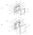
- FIG. 6A is a front view of the solid-state image sensor 1 showing a state in which the heat radiating plate 20 is attached
- FIG. 6B is a perspective view showing an attached structure of the heat radiating plate 20
- FIG. 7A is a perspective view showing a solid-state image sensor 1 and a mounting substrate 30 showing a state in which the heat sink 20 is mounted
- FIG. 8A is a perspective view showing a state in which the solid-state image sensor 1 and the mounting board 30 are set in the housing 40
- FIG. 8B shows a state in which the solid-state image sensor 1 and the mounting board 30 are fixed in the housing 40. It is a perspective view which shows.
- the solid-state image sensor 1 when the solid-state image sensor 1 is mounted on a camera as an external device, a step of attaching a heat sink 20 to the solid-state image sensor 1 is performed.
- the heat radiating plate 20 is provided in the region between the left and right connectors 5 forming the cavity 10 on the back surface 3b of the substrate 3.
- the heat radiating plate 20 is fixed to a predetermined position with respect to the substrate 3 by fastening one of the plate surfaces 20a as a contact surface with respect to the back surface 3b of the substrate 3 by a screw 21 as a fastener.
- a screw 21 for fixing the heat radiating plate 20 to the substrate 3, four holes 16 formed in the substrate 3 are used.
- the screw 21 penetrates the washer 22 interposed between the screw 21 and the surface 3a of the substrate 3 and also penetrates the hole 16 of the substrate 3 to form a screw hole formed in the heat radiating plate 20. Screwed into 20b.
- adhesion with an adhesive may be used.
- the heat radiating plate 20 is, for example, a rectangular plate-shaped member having an external dimension larger than that of the image sensor 2, and is provided so as to include an arrangement area of the image sensor 2.
- the heat radiating plate 20 is a rectangular plate-shaped member having a longitudinal direction in the front-rear direction, has a longer dimension than the substrate 3 in the longitudinal direction, and extends both front and rear portions protruding from the substrate 3.
- the protrusion is 20c.
- the heat sink 20 is made of a metal having high thermal conductivity such as copper, brass, and aluminum.
- the solid-state image sensor 1 to which the heat radiating plate 20 is attached is mounted on the mounting board 30 which is the board on the camera side.
- the mounting board 30 is provided with a connector 31 on the receiving side, which is a fitted portion for receiving the fitting of the connector 5, on the surface 30a, which is a plate surface on which the solid-state image sensor 1 is mounted.
- the connectors 31 are provided at two positions on the surface 30a of the mounting board 30 in a positional relationship corresponding to the arrangement of the two connectors 5 on the board 3.
- the connector 31 is a receptacle for the connector 5 and has a fitting recess 31a for receiving the insertion of the fitting portion 11a of the connector 5.
- the pressed portion 15 of the board 3 pushes the connector 5 into the connector 31 and fits the connector 5. It is the part that is affected by the load.
- the solid-state imaging device 1 set so that each connector 5 is positioned on the corresponding connector 31 with respect to the mounting substrate 30, the pressed portion is pressed from the surface 3a side of the substrate 3 by a predetermined pressing member 35. 15 is subjected to the action of a downward load as a pressing force, and the connector 5 is inserted into the connector 31 so that the two are fitted together.
- the pressing member 35 has a flat pressing surface 35a on one side.
- the pressing surface 35a becomes a contact surface of the pressed portion 15 with respect to the pressed surface 15a in the pressing action of the pressing member 35 on the substrate 3.
- the pressing member 35 is provided so as to move downward with a predetermined pressing force by a predetermined driving source in the device used for attaching the solid-state image pickup device 1 to the mounting substrate 30 (see arrow A1).
- the mounting board 30 to which the solid-state image sensor 1 is mounted receives optical axis alignment on a predetermined board support portion 41 provided in the camera housing 40. That is, the optical axis of the solid-state image sensor 1 is aligned with the lens constituting the optical system in the camera.
- the solid-state image sensor 1 As the optical axis alignment, for example, by moving the mounting substrate 30 to which the solid-state image sensor 1 is mounted in the housing 40, the solid-state image sensor 1 is aligned with the lens optical axis B1 in the housing 40. ..
- the surface portion of the housing 40 on one side is a light receiving side surface portion 40a that receives incident light of light.
- the substrate support portion 41 is provided so as to face the light receiving side surface portion 40a.
- the mounting substrate 30 united with the solid-state image pickup device 1 is provided so that the solid-state image pickup device 1 faces the light-receiving side surface portion 40a with respect to the substrate support portion 41.
- the heat sink 20 is fixed by the screw 42.
- the screw 42 penetrates the fixing holes 20d formed at two positions in each of the extending portions 20c before and after the heat radiating plate 20, and is screwed into a predetermined portion such as the substrate support portion 41 in the housing 40.
- the solid-state image sensor 1 and the mounting substrate 30 are fixed to a predetermined portion such as the substrate support portion 41 in the housing 40.
- the hole portion 16 of the substrate 3 is used for indirect attachment via the heat sink 20 as the attachment of the substrate 3 to the camera. That is, the heat sink 20 is used as a mounting member fixed to the substrate 3 using the hole 16 and fixed to the substrate support portion 41 or the like of the housing 40, and the substrate 3 is mounted in the housing 40. ..
- FIGS. 9 and 10 Another example of the mounting method of the solid-state image sensor 1 according to the first embodiment of the present technology will be described with reference to FIGS. 9 and 10.
- the housing 50 of the camera of this example has a surface portion on one side (back side in FIG. 9A) as a light receiving side surface portion 50a that receives incident light of light.
- a substrate support portion 51 is provided in the housing 50 so as to face the light receiving side surface portion 50a.
- the solid-state image sensor 1 is provided on the back side surface 51a, which is the surface opposite to the light receiving side surface portion 50a side with respect to the substrate support portion 51.
- a screw hole 52 for receiving the fixing of the solid-state image sensor 1 is formed in the substrate support portion 51.
- the screw holes 52 are formed at four locations corresponding to the arrangement of the holes 16 of the substrate 3.
- the substrate support portion 51 is formed with an opening 53 for allowing the arrangement region of the image sensor 2 of the solid-state image sensor 1 fixed to the back side surface portion 51a of the substrate support portion 51 to face the light receiving side surface portion 50a.
- the opening 53 is formed to have a size larger than that of the frame 4.
- the solid-state image sensor 1 is positioned with respect to the substrate support portion 51 of the housing 50.
- the solid-state image sensor 1 is positioned so that the hole portion 16 of the substrate 3 matches the screw hole 52 with the surface 3a side of the substrate 3 facing the light receiving side surface portion 50a side.
- the solid-state image sensor 1 positions the frame 4 in the opening 53 of the substrate support 51 in a positioned state, and brings the surface 3a of the substrate 3 into contact with the back side surface 51a of the substrate support 51.
- the solid-state image sensor 1 positioned in the housing 50 is fixed to the substrate support portion 51 by being fastened by a screw 54 as a fastener.
- Four hole portions 16 of the substrate 3 are used for fixing the solid-state image pickup device 1 to the substrate support portion 51.
- the screw 54 penetrates the hole 16 of the substrate 3 and is screwed into the screw hole 52 of the substrate support 51.
- adhesion with an adhesive may be used.
- the heat radiating plate 60 is a rectangular plate-shaped member having substantially the same size as the substrate 3, and has an opening 61 for avoiding interference with the left and right connectors 5.
- the opening 61 has an elongated rectangular opening shape corresponding to the plan view shape of the connector 5.
- one plate surface is brought into contact with the back surface 3b of the substrate 3, and the connector 5 is passed through the opening 61.
- the connector 5 is in a state in which a portion including the fitting portion 11a is projected from the opening 61.
- the heat radiating plate 60 is attached to the back side of the solid-state image sensor 1 by being fixed to the substrate 3 by fastening with fasteners such as screws or by bonding with an adhesive or the like.
- the heat sink 60 is made of a metal having high thermal conductivity such as copper, brass, and aluminum.
- the mounting board 30 As shown in FIG. 10B, after the heat sink 60 is attached to the solid-state image sensor 1, the mounting board 30 (see FIG. 7A) is attached to the solid-state image sensor 1 (see arrow C2). That is, the connector 31 of the mounting board 30 is fitted to the connector 5 of the solid-state image sensor 1, and both are electrically connected to each other.
- the hole portion 16 of the substrate 3 is used for directly attaching the substrate 3 to the substrate support portion 51 of the housing 50 as the attachment of the substrate 3 to the camera.
- the following modification is a modification of the arrangement of the connector 5 and the hole 16 in the solid-state image sensor 1.
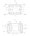
- 11A, 11B, and 11C are all bottom views of the solid-state image sensor 1.
- the first modification shown in FIG. 11A is a configuration in which one hole 16 is provided at each of the front and rear edges of the substrate 3.
- the two holes 16 are provided at positions symmetrical with respect to the center point of the substrate 3 on the substrate 3, for example, as shown in FIG. 11A.
- the second modification shown in FIG. 11B has a configuration in which one hole 16 is provided in each of the two diagonal corners of the substrate 3.
- the left and right connectors 5 are provided at positions deviated from the center of the substrate 3 in the front-rear direction (vertical direction in FIG. 11B) so as not to interfere with the hole portion 16.
- the third modification shown in FIG. 11C is a configuration in which the holes 16 are provided in the mounting areas of the left and right connectors 5.
- the hole 16 is formed in a portion of the mounting area of the connector 5 that avoids a portion of a metal for soldering such as a copper foil.
- the two holes 16 are provided at positions in the vicinity of the two diagonal corners of the substrate 3 and at positions symmetrical with respect to the center point of the substrate 3.
- the connector 5 is shown by a two-dot chain line.
- the package size can be reduced and the transmission delay of the high-speed interface can be suppressed by a simple structure in dealing with the heat generation of the solid-state image sensor 1. can do.
- the package size tends to be large. There is a problem that the wiring length becomes long due to the influence and the transmission delay of the high-speed interface occurs.
- the wiring from the image sensor 2 to the connector 5 is provided.
- the length can be shortened. This makes it easy to reduce the package size and suppress the transmission delay of the high-speed interface.
- the cavity 10 is formed under the chip of the image sensor 2 on the back surface 3b side of the substrate 3 due to the arrangement configuration of the two connectors 5 with respect to the back surface 3b of the substrate 3. NS.
- the heat radiating plate 20 can be easily attached to the image sensor 2 whose heat generation increases with the increase in the number of pixels and the increase in the frame rate by using the cavity 10. This makes it possible to efficiently dissipate heat to the housing of the camera on which the solid-state image sensor 1 is mounted.
- the package structure can be miniaturized while securing the cavity 10 under the chip of the image sensor 2.
- the electrical connection to the external device can be made by fitting the connector 5, it can be easily attached to and detached from the mounting board 30 which is the board on the camera side. Further, it is possible to use a plurality of types of connectors 5 depending on the application and usability.
- the connector 5 is mounted in advance when the image sensor 2 is mounted by performing the step of mounting the image sensor 2 on the board 3 after the step of mounting the connector 5 on the board 3. can do. As a result, even if the image sensor 2 has a relatively low solder heat resistance, the image sensor 2 can be provided without being exposed to the high temperature environment of the reflow for mounting the connector 5.
- the substrate 3 has a pressed portion 15 that receives a load for fitting the connector 5 on the outside of the arrangement region of the frame 4. According to such a configuration, the simple structure makes it possible to fit the connector 5 to the fitted portion without applying excessive stress to the package structure.
- a plurality of holes 16 are formed on the peripheral edge of the substrate 3. According to such a configuration, the hole portion 16 can be used to align the image sensor 2 and the connector 5 with respect to the substrate 3, and the solid-state image sensor 1 can be attached to the camera.
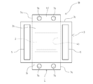
- FIGS. 12 and 13 are both bottom views of the solid-state image sensor 1A.
- the same reference numerals are given to the configurations common to those of the first embodiment, and the description thereof will be omitted as appropriate.
- a plurality of connectors 5 are provided on each of the opposite edges of the substrate 3.
- two connectors 5A and 5B are arranged at the left and right side edges of the substrate 3 at predetermined intervals in the front-rear direction (vertical direction in FIG. 12).
- the two connectors 5A and 5B on the left and right sides are arranged in series with the front-rear direction as the longitudinal direction.
- the four connectors 5 are arranged symmetrically in the left-right direction and the front-back direction.
- a hole 16 is formed in a portion between the connectors 5A and 5B adjacent to each other in the front-rear direction. That is, the hole portion 16 is formed in the central portion in the front-rear direction at both the left and right ends of the substrate 3.
- two connectors 5A and 5B are provided on one side of the left and right sides of the substrate 3, and a hole 16 is provided between the adjacent connectors 5A and 5B.
- two connectors 5 are spaced apart from each other in the left-right direction (left-right direction in FIG. 13A) at the front and rear edges of the substrate 3. Is placed.
- the two connectors 5A and 5B on the front and rear sides are arranged in series with the left-right direction as the longitudinal direction.
- the four connectors 5 are arranged symmetrically in the left-right direction and the front-back direction.
- a hole portion 16 is formed in a portion near both left and right ends and between the front and rear connectors 5A and 5B facing in the front-rear direction. That is, the hole portion 16 is formed in the central portion in the front-rear direction at both the left and right ends of the substrate 3.
- two connectors 5A and 5B are provided on one side of the front and rear of the substrate 3, and a hole 16 is provided between the front and rear connectors 5A and 5B.
- two connectors 5 are arranged at the left and right side edges of the substrate 3 at predetermined intervals in the left-right direction.
- the two connectors 5C and 5D on the left and right sides are arranged in parallel with the front-rear direction as the longitudinal direction. That is, the left and right outer connectors 5C and the left and right inner connectors 5D are provided in two rows.
- two connectors B and 5C are provided on both the left and right sides of the substrate 3 in different arrangements.
- one hole 16 is formed in each of the two diagonal corners of the substrate 3, and the left and right outer connectors 5C are in the front-rear direction so as not to interfere with the hole 16. (Vertical direction in FIG. 13B) is provided at a position deviated from the center of the substrate 3.
- the left and right outer connectors 5C and the two holes 16 are provided so as to be point-symmetrical with respect to the center point of the substrate 3.
- the left and right inner connectors 5D are provided symmetrically in the left-right direction.
- a plurality of connectors 5 may be provided at each edge of the substrate 3.
- two connectors 5 are provided at each edge of the substrate 3, but three or more connectors 5 may be provided at each edge of the substrate 3.
- the image sensor 2 and the connector 5 can be easily aligned and attached to the camera by using the hole portion 16 as in the configuration of the first embodiment. It will be possible.
- the arrangement of the connectors 5 is changed at both ends of the substrate 3 to form an asymmetrical arrangement, so that the orientation of the solid-state image sensor 1A can be obtained when the connectors 5 are fitted. It can be constrained. This makes it possible to prevent an error (reverse insertion) in the mounting direction of the solid-state image sensor 1A with respect to the mounting substrate 30.
- FIG. 15 is a bottom view of the solid-state image sensor 1B.
- the hole portion 76 is provided in the frame 4 instead of the hole portion 16 of the substrate 3. That is, in the frame 4, a hole portion 76 penetrating in the vertical direction is formed on the outside of the arrangement area of the image sensor 2.
- the hole 76 is used for at least one of the alignment of the mounted components on the substrate 3 and the attachment of the substrate 3 to the external device to which the solid-state image sensor 1 is attached.
- the frame 4 has a rectangular outer shape with the front-rear direction as the longitudinal direction, and the front-rear and both side portions are the extending portions 74 protruding from the substrate 3. That is, the frame 4 has a longer dimension than the substrate 3 in the front-rear direction, and the extending portions 74 on both the front and rear sides are projected from the front and rear end faces 3c of the substrate 3 in a plan view.
- a hole 76 is formed in the extending portion 74 of the frame 4.
- the hole portion 76 is a portion forming a circular hole that penetrates the extending portion 74 of the frame 4 in the plate thickness direction.
- two hole portions 76 are provided at positions spaced apart from each other in the left-right direction.
- the hole portion 76 used for positioning the mounted components and attaching to the camera may be provided in the frame 4.
- the frame 4 has an anterior-posterior extending portion 74 as a forming portion of the hole portion 76, but the forming portion of the hole portion 76 is not particularly limited.
- the formed portion of the hole portion 76 may be a portion of the frame 4 extending outward from the substrate 3 in the left-right direction or the diagonal direction (diagonal direction of the substrate 3), for example.
- the configuration in which the hole portion 76 is provided in the frame 4 may be used in combination with the configuration in which the hole portion 16 is provided in the substrate 3. That is, the holes 16 and 76 may be formed on at least one of the substrate 3 and the frame 4.
- the image sensor 2 and the connector 5 can be easily aligned and attached to the camera by using the hole portion 76 of the frame 4, as in the configuration of the first embodiment. It will be possible to do. Further, when it is difficult to secure an area for forming the hole portion 16 in the substrate 3, the configuration of the present embodiment in which the hole portion 76 is provided in the frame 4 is preferably used.
- a recess 80 is formed on the back surface 3b side of the substrate 3 so that at least a part thereof is located in the arrangement region of the image sensor 2. ing.
- the recess 80 is a portion forming a step with respect to the back surface 3b of the substrate 3, and has an upper surface 81 and left and right side surfaces 82 and 83.
- the recess 80 is formed so as to have a depth of, for example, about half to two-thirds of the thickness of the substrate 3.
- the recess 80 may be a groove-shaped portion having at least one of the front and rear sides open, or may be a hole-shaped portion having front and rear side surfaces.
- the recess 80 is formed in a portion on the left side with respect to the center of the substrate 3 in the left-right direction.
- the upper surface 81 is a surface forming the bottom surface of the recess 80, and is formed parallel to the surface 3a of the substrate 3.
- the left side surface 82 which is the left and right outer side surface of the recess 80, is located below the left side side portion 4a of the frame 4 in the left-right direction.
- the right side surface 83 which is the left and right inner side surface of the recess 80, is located below the vicinity of the left edge portion of the image sensor 2 in the left-right direction.
- the recess 80 is formed by forming a concave portion to be the recess 80 in the sheet member before firing in the manufacturing process of the substrate 3.
- the method of forming the recess 80 is not particularly limited. Depending on the material of the substrate 3, for example, a method of forming a recess 80 by performing a hole-drilling process or the like in a plate-shaped substrate member to be the substrate 3 may be used.
- the recess 80 may be a recess 80A formed so as to include the entire arrangement area of the image sensor 2 in the front-rear direction and the left-right direction.
- the left side surface 82 is located on the left side of the left end surface 2d of the image sensor 2 and the right side surface 83 is located on the right side of the right end surface 2e of the image sensor 2 in the left-right direction.
- the upper surface 81 of the recess 80A includes the entire arrangement area of the image sensor 2 in a plan view.
- the solid-state image sensor 1C by providing a recess 80 having a concave shape in a part or the entire surface directly under the image sensor 2 on the back surface 3b of the substrate 3, a chip such as a capacitor or a resistor is provided in the recess 80. It is possible to arrange electronic parts 85 such as parts and electrodes, and parts for heat dissipation such as heat sinks. This makes it possible to mount electronic components and a thick heat sink on the substrate 3 without expanding the package structure.
- Configuration example of the solid-state image sensor according to the fifth embodiment> A configuration example of the solid-state image sensor 1D according to the fifth embodiment of the present technology will be described with reference to FIG.
- stepped portions 90 corresponding to the heights of the plurality of connectors 5 are formed on the back surface 3b side of the substrate 3.
- the height position of the lower end 5b of the connector 5 becomes a common height position according to the height of each of the connectors 5E and 5F, that is, the lower end 5b of the connector 5 is positioned on a common horizontal plane.
- the stepped portion 90 is formed.
- the relatively high connector 5E located on the left side is mounted on the upper first back side surface 91 formed by the step portion 90 as the back surface 3b of the substrate 3.
- the connector 5F having a relatively low height located on the right side is mounted on the lower second back side surface 92 formed by the step portion 90 as the back surface 3b of the substrate 3.
- the first back side surface 91 and the second back side surface 92 are formed via a stepped surface 93 formed along the vertical direction in the stepped portion 90.
- the substrate 3 is a thin-walled portion 94 which is a forming portion of the first back side surface 91 and has a relatively thin plate thickness, and a thin-walled portion 94 which is a forming portion of the second back side surface 92 and has a relatively thick plate thickness. It has a thick portion 95.
- the thin portion 94 and the thick portion 95 of the substrate 3 are formed so that the height difference D1 between the first back side surface 91 and the second back side surface 92 is the same as the height difference between the connectors 5E and 5F. There is. In the example shown in FIG. 18, in the left-right direction, most of the substrate 3 is a thin-walled portion 94, and the right end portion is a thick-walled portion 95.
- the formation range of the first back side surface 91 and the second back side surface 92 is not particularly limited.
- the step portion 90 for example, in a configuration in which three or more connectors 5 having different heights are mounted, the height positions of the lower ends 5b of all the connectors 5 are the same according to the height of the connectors 5.
- the stepped portion 90 may be formed in a plurality of stages. According to such a configuration, three or more steps of back surfaces having different heights are formed as mounting surfaces of the connectors 5 having different heights.
- the stepped portion 90 is formed by forming a stepped portion to be the stepped portion 90 on the sheet member before firing in the manufacturing process of the substrate 3.
- the method of forming the stepped portion 90 is not particularly limited. Depending on the material of the substrate 3, for example, a method of forming a stepped portion 90 by subjecting a plate-shaped substrate member to be the substrate 3 to an etching process or the like may be used.
- a plurality of connectors 5 having different heights can be mounted by providing a stepped portion 90 according to the height of the connector 5 on the back surface 3b side of the substrate 3. It will be possible. Further, it is possible to arrange chip parts such as capacitors and resistors, electronic parts such as electrodes, and heat dissipation parts such as heat sinks on the upper first back side surface 91 formed by the step portion 90. This makes it possible to mount electronic components and a thick heat sink on the substrate 3 without expanding the package structure.
- the solid-state image pickup device 1 is used as an image capture unit (photoelectric conversion unit) such as an image pickup device such as a digital still camera or a video camera, a portable terminal device having an image pickup function, or a copier using a solid-state image sensor as an image reading unit. It can be applied to all electronic devices that use a solid-state image sensor.
- the solid-state image sensor may be in the form of one chip, or may be in the form of a module having an image pickup function in which an image pickup unit and a signal processing unit or an optical system are packaged together. You may.
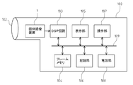
- the image pickup device 100 as an electronic device includes an optical unit 102, a solid-state image pickup device 1, a DSP (Digital Signal Processor) circuit 103 which is a camera signal processing circuit, a frame memory 104, and a display unit. It includes a 105, a recording unit 106, an operation unit 107, and a power supply unit 108.
- the DSP circuit 103, the frame memory 104, the display unit 105, the recording unit 106, the operation unit 107, and the power supply unit 108 are connected to each other via the bus line 109.
- the optical unit 102 includes a plurality of lenses, captures incident light (image light) from the subject, and forms an image on the image pickup surface of the solid-state image pickup device 1.
- the solid-state image sensor 1 converts the amount of incident light imaged on the image pickup surface by the optical unit 102 into an electric signal in pixel units and outputs it as a pixel signal.
- the display unit 105 comprises a panel-type display device such as a liquid crystal panel or an organic EL (Electro Luminescence) panel, and displays a moving image or a still image captured by the solid-state image pickup device 1.
- the recording unit 106 records a moving image or a still image captured by the solid-state image sensor 1 on a recording medium such as a hard disk or a semiconductor memory.
- the operation unit 107 issues operation commands for various functions of the image pickup apparatus 100 under the operation of the user.
- the power supply unit 108 appropriately supplies various power sources that serve as operating power sources for the DSP circuit 103, the frame memory 104, the display unit 105, the recording unit 106, and the operation unit 107 to these supply targets.
- the package size can be reduced and the transmission delay of the high-speed interface can be suppressed by a simple structure in dealing with the heat generation of the solid-state image pickup apparatus 1. can do.
- the miniaturization of the image pickup apparatus 100 can be promoted.
- the present technology can have the following configurations. (1) A solid-state image sensor with one plate surface side of the semiconductor substrate as the light receiving side, A substrate on which the solid-state image sensor is mounted on a surface that is one of the plate surfaces, and a substrate. A support member provided on the surface side of the substrate so as to surround the solid-state image sensor, and A plurality of connectors provided on the back surface, which is the other plate surface of the substrate, and located outside the arrangement region of the solid-state image sensor on the substrate, are provided.
- the connector is a solid-state image pickup device in which at least a part thereof is located outside the placement area of the support member on the substrate.
- the connector is an electronic device including a solid-state image pickup device in which at least a part thereof is located outside the placement area of the support member on the substrate.
- Solid-state image sensor 2 Image sensor (solid-state image sensor) 3 Substrate 3a Front side 3b Back side 4 Frame (support member) 5 Connector 15 Pressed part 16 Hole part 74 Extension part 76 Hole part 80 Concave part 90 Step part 100 Image pickup device
Landscapes
- Engineering & Computer Science (AREA)
- Multimedia (AREA)
- Signal Processing (AREA)
- Solid State Image Pick-Up Elements (AREA)
Abstract
Description
1.第1実施形態に係る固体撮像装置の構成例
2.第1実施形態に係る固体撮像装置の製造方法
3.第1実施形態に係る固体撮像装置の実装方法
4.第1実施形態に係る固体撮像装置の変形例
5.第2実施形態に係る固体撮像装置の構成例
6.第2実施形態に係る固体撮像装置の変形例
7.第3実施形態に係る固体撮像装置の構成例
8.第4実施形態に係る固体撮像装置の構成例
9.第5実施形態に係る固体撮像装置の構成例
10.電子機器の構成例
本技術の第1実施形態に係る固体撮像装置1の構成例について、図1から図3を参照して説明する。図1から図3に示すように、固体撮像装置1は、固体撮像素子としてのイメージセンサ2と、イメージセンサ2の実装を受ける基板3と、基板3上に設けられた支持部材としてのフレーム4と、固体撮像装置1を外部装置に電気的に接続するための複数のコネクタ5とを備える。また、固体撮像装置1は、フレーム4上に支持された透光性部材としてのガラス6を備える。
本技術の第1実施形態に係る固体撮像装置1の製造方法の一例について、図4および図5を用いて説明する。
本技術の第1実施形態に係る固体撮像装置1の実装方法の一例について、図6から図8を用いて説明する。図6Aは、放熱板20を取り付けた状態を示す固体撮像装置1の正面図であり、図6Bは、放熱板20の取付け構造を示す斜視図である。図7Aは、放熱板20を取り付けた状態を示す固体撮像装置1および取付基板30を示す斜視図である。図8Aは、筐体40内に固体撮像装置1および取付基板30をセットした状態を示す斜視図であり、図8Bは、筐体40内に固体撮像装置1および取付基板30を固定した状態を示す斜視図である。
本技術の第1実施形態に係る固体撮像装置1の変形例を図11A、図11Bおよび図11Cに示す。次に示す変形例は、固体撮像装置1におけるコネクタ5および孔部16の配置等についての変形例である。図11A、図11Bおよび図11Cは、いずれも固体撮像装置1の底面図である。
本技術の第2実施形態に係る固体撮像装置1の構成例ついて、図12および図13を参照して説明する。図12および図13は、いずれも固体撮像装置1Aの底面図である。なお、以下に説明する各実施形態において、第1実施形態と共通する構成については同一の符号を付して適宜説明を省略する。
本技術の第2実施形態に係る固体撮像装置1Aの変形例を図13Aおよび図13Bに示す。図13Aおよび図13Bは、いずれも固体撮像装置1Aの底面図である。
本技術の第3実施形態に係る固体撮像装置1Bの構成例ついて、図14および図15を参照して説明する。図15は、固体撮像装置1Bの底面図である。
本技術の第4実施形態に係る固体撮像装置1Cの構成例ついて、図16および図17を参照して説明する。
本技術の第5実施形態に係る固体撮像装置1Dの構成例ついて、図18を参照して説明する。
上述した実施形態に係る固体撮像装置の電子機器への適用例について、図19を用いて説明する。なお、ここでは第1実施形態に係る固体撮像装置1の適用例について説明する。
(1)
半導体基板の一方の板面側を受光側とする固体撮像素子と、
一方の板面である表面に前記固体撮像素子が実装される基板と、
前記基板の前記表面側に前記固体撮像素子を囲むように設けられた支持部材と、
前記基板の他方の板面である裏面に設けられ、前記基板における前記固体撮像素子の配置領域の外側に位置する複数のコネクタと、を備え、
前記コネクタは、少なくとも一部を、前記基板における前記支持部材の配置領域の外側に位置させる
固体撮像装置。
(2)
前記基板は、前記表面側における前記支持部材の配置領域の外側に、前記コネクタを、該コネクタに対する被嵌合部に嵌合させるための荷重を受ける被押圧部を有する
前記(1)に記載の固体撮像装置。
(3)
前記基板および前記支持部材の少なくともいずれか一方には、前記固体撮像素子の配置領域の外側に、前記基板の板厚方向に貫通し、前記基板における実装部品の位置合わせ、および外部装置に対する前記基板の取付けの少なくともいずれか一方に用いられる孔部が形成されている
前記(1)または前記(2)に記載の固体撮像装置。
(4)
前記基板の前記裏面側には、少なくとも一部を前記固体撮像素子の配置領域内に位置させるように、凹部が形成されている
前記(1)~(3)のいずれか1つに記載の固体撮像装置。
(5)
前記基板の前記裏面側には、前記複数のコネクタの高さに応じた段差部が形成されている
前記(1)~(4)のいずれか1つに記載の固体撮像装置。
(6)
半導体基板の一方の板面側を受光側とする固体撮像素子と、
一方の板面である表面に前記固体撮像素子が実装される基板と、
前記基板の前記表面側に前記固体撮像素子を囲むように設けられた支持部材と、
前記基板の他方の板面である裏面に設けられ、前記基板における前記固体撮像素子の配置領域の外側に位置する複数のコネクタと、を備え、
前記コネクタは、少なくとも一部を、前記基板における前記支持部材の配置領域の外側に位置させる
固体撮像装置を備えた
電子機器。
2 イメージセンサ(固体撮像素子)
3 基板
3a 表面
3b 裏面
4 フレーム(支持部材)
5 コネクタ
15 被押圧部
16 孔部
74 延出部
76 孔部
80 凹部
90 段差部
100 撮像装置
Claims (6)
- 半導体基板の一方の板面側を受光側とする固体撮像素子と、
一方の板面である表面に前記固体撮像素子が実装される基板と、
前記基板の前記表面側に前記固体撮像素子を囲むように設けられた支持部材と、
前記基板の他方の板面である裏面に設けられ、前記基板における前記固体撮像素子の配置領域の外側に位置する複数のコネクタと、を備え、
前記コネクタは、少なくとも一部を、前記基板における前記支持部材の配置領域の外側に位置させる
固体撮像装置。 - 前記基板は、前記表面側における前記支持部材の配置領域の外側に、前記コネクタを、該コネクタに対する被嵌合部に嵌合させるための荷重を受ける被押圧部を有する
請求項1に記載の固体撮像装置。 - 前記基板および前記支持部材の少なくともいずれか一方には、前記固体撮像素子の配置領域の外側に、前記基板の板厚方向に貫通し、前記基板における実装部品の位置合わせ、および外部装置に対する前記基板の取付けの少なくともいずれか一方に用いられる孔部が形成されている
請求項1に記載の固体撮像装置。 - 前記基板の前記裏面側には、少なくとも一部を前記固体撮像素子の配置領域内に位置させるように、凹部が形成されている
請求項1に記載の固体撮像装置。 - 前記基板の前記裏面側には、前記複数のコネクタの高さに応じた段差部が形成されている
請求項1に記載の固体撮像装置。 - 半導体基板の一方の板面側を受光側とする固体撮像素子と、
一方の板面である表面に前記固体撮像素子が実装される基板と、
前記基板の前記表面側に前記固体撮像素子を囲むように設けられた支持部材と、
前記基板の他方の板面である裏面に設けられ、前記基板における前記固体撮像素子の配置領域の外側に位置する複数のコネクタと、を備え、
前記コネクタは、少なくとも一部を、前記基板における前記支持部材の配置領域の外側に位置させる
固体撮像装置を備えた
電子機器。
Priority Applications (2)
| Application Number | Priority Date | Filing Date | Title |
|---|---|---|---|
| US17/998,987 US12557411B2 (en) | 2020-05-28 | 2021-04-15 | Solid-state imaging device and electronic apparatus |
| EP21814618.1A EP4160666A4 (en) | 2020-05-28 | 2021-04-15 | SOLID STATE IMAGING APPARATUS AND ELECTRONIC DEVICE |
Applications Claiming Priority (2)
| Application Number | Priority Date | Filing Date | Title |
|---|---|---|---|
| JP2020-092847 | 2020-05-28 | ||
| JP2020092847 | 2020-05-28 |
Publications (1)
| Publication Number | Publication Date |
|---|---|
| WO2021241053A1 true WO2021241053A1 (ja) | 2021-12-02 |
Family
ID=78744272
Family Applications (1)
| Application Number | Title | Priority Date | Filing Date |
|---|---|---|---|
| PCT/JP2021/015528 Ceased WO2021241053A1 (ja) | 2020-05-28 | 2021-04-15 | 固体撮像装置および電子機器 |
Country Status (3)
| Country | Link |
|---|---|
| US (1) | US12557411B2 (ja) |
| EP (1) | EP4160666A4 (ja) |
| WO (1) | WO2021241053A1 (ja) |
Cited By (2)
| Publication number | Priority date | Publication date | Assignee | Title |
|---|---|---|---|---|
| WO2024181074A1 (ja) | 2023-02-27 | 2024-09-06 | ソニーセミコンダクタソリューションズ株式会社 | 半導体装置、電子機器および半導体装置の製造方法 |
| WO2026018560A1 (ja) * | 2024-07-17 | 2026-01-22 | ソニーセミコンダクタソリューションズ株式会社 | 半導体パッケージ、半導体装置、および、半導体パッケージの製造方法 |
Families Citing this family (1)
| Publication number | Priority date | Publication date | Assignee | Title |
|---|---|---|---|---|
| US12501133B2 (en) * | 2023-04-10 | 2025-12-16 | Samsung Electro-Mechanics Co., Ltd. | Image sensor module and camera module including the same |
Citations (6)
| Publication number | Priority date | Publication date | Assignee | Title |
|---|---|---|---|---|
| JPH05284396A (ja) * | 1992-03-31 | 1993-10-29 | Sony Corp | 撮像装置 |
| JPH10144898A (ja) * | 1996-11-15 | 1998-05-29 | Sony Corp | 固体撮像装置 |
| JP2001177023A (ja) | 1999-12-21 | 2001-06-29 | Casio Comput Co Ltd | チップ素子の取付構造 |
| JP2008172090A (ja) * | 2007-01-12 | 2008-07-24 | Nikon Corp | 半導体素子用パッケージ及び半導体装置 |
| JP2009070876A (ja) * | 2007-09-11 | 2009-04-02 | Panasonic Corp | 固体撮像装置およびその製造方法 |
| JP2012044381A (ja) | 2010-08-18 | 2012-03-01 | Hitachi Kokusai Electric Inc | 固体撮像素子の放熱構造 |
Family Cites Families (8)
| Publication number | Priority date | Publication date | Assignee | Title |
|---|---|---|---|---|
| JPH06151796A (ja) * | 1992-10-30 | 1994-05-31 | Sony Corp | 固体撮像装置及び固体撮像素子用パッケージ |
| JP3881888B2 (ja) * | 2001-12-27 | 2007-02-14 | セイコーエプソン株式会社 | 光デバイスの製造方法 |
| JP3729817B2 (ja) * | 2003-04-28 | 2005-12-21 | 松下電器産業株式会社 | 固体撮像装置の製造方法 |
| JP4236594B2 (ja) * | 2004-01-27 | 2009-03-11 | シャープ株式会社 | 光学装置用モジュール及び光学装置用モジュールの製造方法 |
| JP4951989B2 (ja) * | 2006-02-09 | 2012-06-13 | 富士通セミコンダクター株式会社 | 半導体装置 |
| US10074757B2 (en) | 2014-09-29 | 2018-09-11 | Sony Corporation | Semiconductor package, sensor module, and production method |
| JP7573438B2 (ja) | 2018-06-08 | 2024-10-25 | ソニーセミコンダクタソリューションズ株式会社 | 撮像装置 |
| JP2022114386A (ja) * | 2021-01-26 | 2022-08-05 | ソニーセミコンダクタソリューションズ株式会社 | 撮像装置 |
-
2021
- 2021-04-15 US US17/998,987 patent/US12557411B2/en active Active
- 2021-04-15 WO PCT/JP2021/015528 patent/WO2021241053A1/ja not_active Ceased
- 2021-04-15 EP EP21814618.1A patent/EP4160666A4/en not_active Withdrawn
Patent Citations (6)
| Publication number | Priority date | Publication date | Assignee | Title |
|---|---|---|---|---|
| JPH05284396A (ja) * | 1992-03-31 | 1993-10-29 | Sony Corp | 撮像装置 |
| JPH10144898A (ja) * | 1996-11-15 | 1998-05-29 | Sony Corp | 固体撮像装置 |
| JP2001177023A (ja) | 1999-12-21 | 2001-06-29 | Casio Comput Co Ltd | チップ素子の取付構造 |
| JP2008172090A (ja) * | 2007-01-12 | 2008-07-24 | Nikon Corp | 半導体素子用パッケージ及び半導体装置 |
| JP2009070876A (ja) * | 2007-09-11 | 2009-04-02 | Panasonic Corp | 固体撮像装置およびその製造方法 |
| JP2012044381A (ja) | 2010-08-18 | 2012-03-01 | Hitachi Kokusai Electric Inc | 固体撮像素子の放熱構造 |
Non-Patent Citations (1)
| Title |
|---|
| See also references of EP4160666A4 |
Cited By (3)
| Publication number | Priority date | Publication date | Assignee | Title |
|---|---|---|---|---|
| WO2024181074A1 (ja) | 2023-02-27 | 2024-09-06 | ソニーセミコンダクタソリューションズ株式会社 | 半導体装置、電子機器および半導体装置の製造方法 |
| EP4675677A1 (en) | 2023-02-27 | 2026-01-07 | Sony Semiconductor Solutions Corporation | Semiconductor device, electronic apparatus, and method for producing semiconductor device |
| WO2026018560A1 (ja) * | 2024-07-17 | 2026-01-22 | ソニーセミコンダクタソリューションズ株式会社 | 半導体パッケージ、半導体装置、および、半導体パッケージの製造方法 |
Also Published As
| Publication number | Publication date |
|---|---|
| EP4160666A4 (en) | 2023-10-25 |
| EP4160666A1 (en) | 2023-04-05 |
| US12557411B2 (en) | 2026-02-17 |
| US20230215886A1 (en) | 2023-07-06 |
Similar Documents
| Publication | Publication Date | Title |
|---|---|---|
| KR101711007B1 (ko) | 이미지 센서 패키지를 갖는 이미지 센서 모듈 | |
| US7593636B2 (en) | Pin referenced image sensor to reduce tilt in a camera module | |
| KR102467001B1 (ko) | 이미지 센서 모듈용 기판 구조체 및 이를 포함하는 이미지 센서 모듈 | |
| CN100592512C (zh) | 具有摄像元件的半导体装置 | |
| CN101847644A (zh) | 半导体器件 | |
| KR20060049316A (ko) | 반도체 이미지 센서 모듈, 반도체 이미지 센서 모듈의 제조방법, 카메라 및 카메라의 제조 방법 | |
| JPH08227984A (ja) | 固体撮像装置 | |
| US20060169991A1 (en) | Light emitting diode | |
| WO2021241053A1 (ja) | 固体撮像装置および電子機器 | |
| WO2020039733A1 (ja) | 半導体装置、電子機器、および半導体装置の製造方法 | |
| TWM460298U (zh) | 電子裝置及其相機裝置 | |
| WO2017090223A1 (ja) | 撮像素子パッケージ、撮像装置及び撮像素子パッケージの製造方法 | |
| CN108231914B (zh) | 3d成像光电模块 | |
| JP2007282195A (ja) | カメラレンズモジュールおよびその製造方法 | |
| EP4398290A1 (en) | Semiconductor device and electronic equipment | |
| WO2022259684A1 (ja) | 固体撮像装置および電子機器 | |
| JP4191954B2 (ja) | 撮像素子実装構造および撮像装置 | |
| EP4675677A1 (en) | Semiconductor device, electronic apparatus, and method for producing semiconductor device | |
| TW201505441A (zh) | 影像感測模組 | |
| EP4235769A1 (en) | Imaging device, electronic apparatus, and method for manufacturing imaging device | |
| JP2011109225A (ja) | 半導体装置 | |
| JP2001177023A (ja) | チップ素子の取付構造 | |
| CN101026149A (zh) | 影像感应器封装结构 | |
| JP2019050418A (ja) | 撮像装置 | |
| JP6184106B2 (ja) | 固体撮像素子用中空パッケージ、固体撮像素子及び固体撮像装置 |
Legal Events
| Date | Code | Title | Description |
|---|---|---|---|
| 121 | Ep: the epo has been informed by wipo that ep was designated in this application |
Ref document number: 21814618 Country of ref document: EP Kind code of ref document: A1 |
|
| NENP | Non-entry into the national phase |
Ref country code: DE |
|
| ENP | Entry into the national phase |
Ref document number: 2021814618 Country of ref document: EP Effective date: 20230102 |
|
| NENP | Non-entry into the national phase |
Ref country code: JP |
|
| WWW | Wipo information: withdrawn in national office |
Ref document number: 2021814618 Country of ref document: EP |
|
| WWG | Wipo information: grant in national office |
Ref document number: 17998987 Country of ref document: US |