WO2021220853A1 - 信号処理装置、信号処理方法、及び表示装置 - Google Patents
信号処理装置、信号処理方法、及び表示装置 Download PDFInfo
- Publication number
- WO2021220853A1 WO2021220853A1 PCT/JP2021/015795 JP2021015795W WO2021220853A1 WO 2021220853 A1 WO2021220853 A1 WO 2021220853A1 JP 2021015795 W JP2021015795 W JP 2021015795W WO 2021220853 A1 WO2021220853 A1 WO 2021220853A1
- Authority
- WO
- WIPO (PCT)
- Prior art keywords
- signal processing
- brightness
- display panel
- signal
- temperature rise
- Prior art date
- Legal status (The legal status is an assumption and is not a legal conclusion. Google has not performed a legal analysis and makes no representation as to the accuracy of the status listed.)
- Ceased
Links
Images








Classifications
-
- G—PHYSICS
- G09—EDUCATION; CRYPTOGRAPHY; DISPLAY; ADVERTISING; SEALS
- G09G—ARRANGEMENTS OR CIRCUITS FOR CONTROL OF INDICATING DEVICES USING STATIC MEANS TO PRESENT VARIABLE INFORMATION
- G09G3/00—Control arrangements or circuits, of interest only in connection with visual indicators other than cathode-ray tubes
- G09G3/20—Control arrangements or circuits, of interest only in connection with visual indicators other than cathode-ray tubes for presentation of an assembly of a number of characters, e.g. a page, by composing the assembly by combination of individual elements arranged in a matrix no fixed position being assigned to or needed to be assigned to the individual characters or partial characters
- G09G3/22—Control arrangements or circuits, of interest only in connection with visual indicators other than cathode-ray tubes for presentation of an assembly of a number of characters, e.g. a page, by composing the assembly by combination of individual elements arranged in a matrix no fixed position being assigned to or needed to be assigned to the individual characters or partial characters using controlled light sources
- G09G3/30—Control arrangements or circuits, of interest only in connection with visual indicators other than cathode-ray tubes for presentation of an assembly of a number of characters, e.g. a page, by composing the assembly by combination of individual elements arranged in a matrix no fixed position being assigned to or needed to be assigned to the individual characters or partial characters using controlled light sources using electroluminescent panels
- G09G3/32—Control arrangements or circuits, of interest only in connection with visual indicators other than cathode-ray tubes for presentation of an assembly of a number of characters, e.g. a page, by composing the assembly by combination of individual elements arranged in a matrix no fixed position being assigned to or needed to be assigned to the individual characters or partial characters using controlled light sources using electroluminescent panels semiconductive, e.g. using light-emitting diodes [LED]
- G09G3/3208—Control arrangements or circuits, of interest only in connection with visual indicators other than cathode-ray tubes for presentation of an assembly of a number of characters, e.g. a page, by composing the assembly by combination of individual elements arranged in a matrix no fixed position being assigned to or needed to be assigned to the individual characters or partial characters using controlled light sources using electroluminescent panels semiconductive, e.g. using light-emitting diodes [LED] organic, e.g. using organic light-emitting diodes [OLED]
-
- G—PHYSICS
- G09—EDUCATION; CRYPTOGRAPHY; DISPLAY; ADVERTISING; SEALS
- G09G—ARRANGEMENTS OR CIRCUITS FOR CONTROL OF INDICATING DEVICES USING STATIC MEANS TO PRESENT VARIABLE INFORMATION
- G09G3/00—Control arrangements or circuits, of interest only in connection with visual indicators other than cathode-ray tubes
- G09G3/20—Control arrangements or circuits, of interest only in connection with visual indicators other than cathode-ray tubes for presentation of an assembly of a number of characters, e.g. a page, by composing the assembly by combination of individual elements arranged in a matrix no fixed position being assigned to or needed to be assigned to the individual characters or partial characters
- G09G3/2092—Details of a display terminals using a flat panel, the details relating to the control arrangement of the display terminal and to the interfaces thereto
- G09G3/2096—Details of the interface to the display terminal specific for a flat panel
-
- G—PHYSICS
- G09—EDUCATION; CRYPTOGRAPHY; DISPLAY; ADVERTISING; SEALS
- G09G—ARRANGEMENTS OR CIRCUITS FOR CONTROL OF INDICATING DEVICES USING STATIC MEANS TO PRESENT VARIABLE INFORMATION
- G09G5/00—Control arrangements or circuits for visual indicators common to cathode-ray tube indicators and other visual indicators
- G09G5/02—Control arrangements or circuits for visual indicators common to cathode-ray tube indicators and other visual indicators characterised by the way in which colour is displayed
- G09G5/04—Control arrangements or circuits for visual indicators common to cathode-ray tube indicators and other visual indicators characterised by the way in which colour is displayed using circuits for interfacing with colour displays
-
- G—PHYSICS
- G09—EDUCATION; CRYPTOGRAPHY; DISPLAY; ADVERTISING; SEALS
- G09G—ARRANGEMENTS OR CIRCUITS FOR CONTROL OF INDICATING DEVICES USING STATIC MEANS TO PRESENT VARIABLE INFORMATION
- G09G5/00—Control arrangements or circuits for visual indicators common to cathode-ray tube indicators and other visual indicators
- G09G5/10—Intensity circuits
-
- G—PHYSICS
- G09—EDUCATION; CRYPTOGRAPHY; DISPLAY; ADVERTISING; SEALS
- G09G—ARRANGEMENTS OR CIRCUITS FOR CONTROL OF INDICATING DEVICES USING STATIC MEANS TO PRESENT VARIABLE INFORMATION
- G09G2300/00—Aspects of the constitution of display devices
- G09G2300/04—Structural and physical details of display devices
- G09G2300/0439—Pixel structures
- G09G2300/0452—Details of colour pixel setup, e.g. pixel composed of a red, a blue and two green components
-
- G—PHYSICS
- G09—EDUCATION; CRYPTOGRAPHY; DISPLAY; ADVERTISING; SEALS
- G09G—ARRANGEMENTS OR CIRCUITS FOR CONTROL OF INDICATING DEVICES USING STATIC MEANS TO PRESENT VARIABLE INFORMATION
- G09G2310/00—Command of the display device
- G09G2310/08—Details of timing specific for flat panels, other than clock recovery
-
- G—PHYSICS
- G09—EDUCATION; CRYPTOGRAPHY; DISPLAY; ADVERTISING; SEALS
- G09G—ARRANGEMENTS OR CIRCUITS FOR CONTROL OF INDICATING DEVICES USING STATIC MEANS TO PRESENT VARIABLE INFORMATION
- G09G2320/00—Control of display operating conditions
- G09G2320/04—Maintaining the quality of display appearance
- G09G2320/041—Temperature compensation
-
- G—PHYSICS
- G09—EDUCATION; CRYPTOGRAPHY; DISPLAY; ADVERTISING; SEALS
- G09G—ARRANGEMENTS OR CIRCUITS FOR CONTROL OF INDICATING DEVICES USING STATIC MEANS TO PRESENT VARIABLE INFORMATION
- G09G2320/00—Control of display operating conditions
- G09G2320/06—Adjustment of display parameters
- G09G2320/0626—Adjustment of display parameters for control of overall brightness
-
- G—PHYSICS
- G09—EDUCATION; CRYPTOGRAPHY; DISPLAY; ADVERTISING; SEALS
- G09G—ARRANGEMENTS OR CIRCUITS FOR CONTROL OF INDICATING DEVICES USING STATIC MEANS TO PRESENT VARIABLE INFORMATION
- G09G2320/00—Control of display operating conditions
- G09G2320/06—Adjustment of display parameters
- G09G2320/0626—Adjustment of display parameters for control of overall brightness
- G09G2320/0653—Controlling or limiting the speed of brightness adjustment of the illumination source
-
- G—PHYSICS
- G09—EDUCATION; CRYPTOGRAPHY; DISPLAY; ADVERTISING; SEALS
- G09G—ARRANGEMENTS OR CIRCUITS FOR CONTROL OF INDICATING DEVICES USING STATIC MEANS TO PRESENT VARIABLE INFORMATION
- G09G2320/00—Control of display operating conditions
- G09G2320/10—Special adaptations of display systems for operation with variable images
- G09G2320/103—Detection of image changes, e.g. determination of an index representative of the image change
-
- G—PHYSICS
- G09—EDUCATION; CRYPTOGRAPHY; DISPLAY; ADVERTISING; SEALS
- G09G—ARRANGEMENTS OR CIRCUITS FOR CONTROL OF INDICATING DEVICES USING STATIC MEANS TO PRESENT VARIABLE INFORMATION
- G09G2340/00—Aspects of display data processing
- G09G2340/06—Colour space transformation
-
- G—PHYSICS
- G09—EDUCATION; CRYPTOGRAPHY; DISPLAY; ADVERTISING; SEALS
- G09G—ARRANGEMENTS OR CIRCUITS FOR CONTROL OF INDICATING DEVICES USING STATIC MEANS TO PRESENT VARIABLE INFORMATION
- G09G2360/00—Aspects of the architecture of display systems
- G09G2360/16—Calculation or use of calculated indices related to luminance levels in display data
-
- H—ELECTRICITY
- H04—ELECTRIC COMMUNICATION TECHNIQUE
- H04N—PICTORIAL COMMUNICATION, e.g. TELEVISION
- H04N5/00—Details of television systems
- H04N5/44—Receiver circuitry for the reception of television signals according to analogue transmission standards
- H04N5/57—Control of contrast or brightness
Definitions
- the present technology relates to a signal processing device, a signal processing method, and a display device, and more particularly to a signal processing device, a signal processing method, and a display device capable of suppressing a temperature rise of a display panel.
- Patent Document 1 discloses a technique for increasing the brightness of a display panel as a technique for a display device such as a self-luminous display device.
- the display device it is required to suppress the temperature rise of the display panel when the brightness of the display panel is increased.
- This technology was made in view of such a situation, and makes it possible to suppress the temperature rise of the display panel.
- the signal processing device on one aspect of the present technology measures the time for improving the brightness of the display panel when the video signal is changed from the low-brightness display signal to the high-brightness display signal. To acquire at least one piece of information from the amount of temperature rise of the panel and the feature amount of the video signal according to the image displayed on the display panel, and to improve the brightness of the image signal based on the acquired information.
- This is a signal processing device including a signal processing unit that adaptively controls the first gain of the above according to the degree of influence of the temperature rise of the display panel.
- the signal processing device increases the brightness of the video signal from the low-brightness display signal to the high-brightness display signal
- the brightness is measured by measuring the time during which the brightness of the display panel is improved. At least one of the improvement time, the amount of temperature rise of the display panel, and the feature amount of the video signal corresponding to the image displayed on the display panel is acquired, and based on the acquired information, the image signal of the image signal is acquired.
- This is a signal processing method in which the first gain for improving the brightness is adaptively controlled according to the degree of influence of the temperature rise of the display panel.
- the time for improving the brightness in the display panel is measured. At least one of the brightness improvement time, the amount of temperature rise of the display panel, and the feature amount of the video signal corresponding to the image displayed on the display panel is acquired, and the image is based on the acquired information.
- the first gain for improving the brightness of the signal is adaptively controlled according to the degree of influence of the temperature rise of the display panel.
- the display device on one aspect of the present technology includes a panel unit having a display panel and a signal processing unit that processes a video signal, and the signal processing unit displays the video signal from a low-brightness display signal to a high-brightness display.
- the brightness improvement time measured by measuring the time for improving the brightness of the display panel, the amount of temperature rise of the display panel, and the feature amount of the video signal according to the image displayed on the display panel.
- the first gain for improving the brightness of the video signal is adaptively controlled according to the degree of influence of the temperature rise of the display panel. It is a display device provided with a signal processing unit.
- the display device when the video signal is increased in brightness from a low-luminance display signal to a high-luminance display signal, the brightness improvement time obtained by measuring the time for which the brightness in the display panel is improved is the display. At least one piece of information is acquired from the amount of temperature rise of the panel and the feature amount of the video signal according to the image displayed on the display panel, and the brightness of the image signal is improved based on the acquired information.
- the first gain for this is adaptively controlled according to the degree of influence of the temperature rise of the display panel.
- the signal processing device and the display device on one aspect of the present technology may be independent devices or internal blocks constituting one device.
- FIG. 1 shows an example of high-luminance processing to which such high-luminance technology is applied.
- FIG. 1A shows the relationship between the input video signal and the integrated value by thick lines L11 and thick lines L12 on the same time axis.
- FIG. 1 shows the relationship between the gain multiplied by the input video signal and the integrated value by thick lines L13 and L14 on the same time axis.
- FIG. 1C shows the relationship between the output video signal obtained by multiplying the input video signal and the gain and the integrated value by thick lines L15 and L16 on the same time axis.
- the high-luminance processing shown in FIG. 1 it is possible to control the brightness improvement period for each high-luminance signal, but in the case of a pattern in which the high-luminance signal is repeatedly displayed, the brightness is improved.
- the period is virtually always continuous.
- FIG. 2 shows an example in which a repeating pattern of a high-luminance signal is displayed by the high-luminance processing.
- FIG. 2A shows the relationship between the input video signal and the integrated value by a thick line L21 and a thick line L22 in which corresponding waveforms are repeated on the same time axis.
- FIG. 2 B in FIG. 2 shows the relationship between the gain and the integrated value by a thick line L23 and a thick line L24 in which the corresponding waveforms are repeated on the same time axis.
- FIG. 2C shows the relationship between the output video signal and the integrated value by a thick line L25 and a thick line L26 in which corresponding waveforms are repeated on the same time axis.
- W conversion WCT: White Color Translation
- the sub-pixels in each pixel are performed.
- WCT White Color Translation
- a three-color lighting method is used in which one color of W and a maximum of two colors from the sub-pixels R, G, and B emit a total of three colors.
- the sub-pixel W has high efficiency without passing through a color filter. Therefore, the brightness is increased by increasing the lighting amount of the sub-pixel W.
- the amount of current of the sub-pixel W which has been increased in brightness by increasing the efficiency of the sub-pixel W without a filter and increasing the size of the sub-pixel W, is less than or equal to the maximum current amount of a single color of the sub-pixels R, G, and B. Therefore, the problem of temperature rise of the OLED display panel is unlikely to occur.
- the unused sub-pixels R, G, and B are turned on to achieve a four-color lighting state, further increasing the brightness. It can be realized.
- the load for the three sub-pixels R, G, and B increases, and the effect on the temperature rise of the OLED display panel is more than three times that of the conventional one. Therefore, the above-mentioned problems are more likely to occur. It ends up.
- FIG. 3 shows a comparative example of the three-color lighting method and the four-color lighting method.
- the input RGB video signal is represented by “Input”
- the lighting of the sub-pixels W, R, G, and B based on the video signal after W conversion is represented by “Output”.
- the four-color lighting method of "x3” is OLED compared to the three-color lighting method of "x1" and "x2". It shows that the influence of the temperature rise of the display panel is large.
- This technology proposes a method for solving the problem of temperature rise, which is a problem when increasing the brightness of the display panel as described above.
- embodiments of the present technology will be described with reference to the drawings.
- FIG. 4 shows a configuration example of an embodiment of a display device to which the present technology is applied.
- the display device 1 is a self-luminous display device such as an OLED display device having an OLED display panel.
- the display device 1 is configured as a television receiver, a display device, or the like.
- the display device 1 is composed of a signal input unit 110, a signal processing unit 111, a panel drive unit 112, and a panel unit 113.
- the signal input unit 110 is composed of a tuner connected to an antenna, a communication module that can be connected to a communication network such as the Internet, an input interface conforming to a predetermined standard, and the like.
- the signal input unit 110 records broadcast content transmitted by terrestrial broadcasting, satellite broadcasting, etc., communication content streamed via a communication network such as the Internet, or a recording medium such as an optical disk or semiconductor memory, a recorder, or the like. Video signals of various contents such as recorded contents are supplied to the signal processing unit 111.
- the signal processing unit 111 performs video signal processing on the video signal of the content supplied from the signal input unit 110, and supplies the video signal obtained as a result to the panel drive unit 112.
- high-luminance processing for changing the video signal from a low-luminance display signal (low-luminance signal) to a high-luminance display signal (high-luminance signal) is performed.
- the panel drive unit 112 drives the panel unit 113 based on the video signal supplied from the signal processing unit 111.
- the panel unit 113 includes a display panel such as an OLED display panel.
- the panel unit 113 displays images according to the images of various contents according to the drive from the panel drive unit 112.
- the OLED display panel is a display panel in which pixels including an OLED element as a self-luminous element are arranged two-dimensionally.
- An OLED Organic Light Emitting Diode
- An OLED is a light emitting element having a structure in which an organic light emitting material is sandwiched between a cathode and an anode, and constitutes pixels (display pixels) arranged two-dimensionally on an OLED display panel. ing.
- each pixel is composed of four sub-pixels of white (W), red (R), green (G), and blue (B) in the case of the WRGB method, and is an RGB method. In the case of, it is composed of three sub-pixels of red (R), green (G), and blue (B).
- the minimum configuration unit is shown for simplification of explanation, but a sound signal processing circuit that processes a sound signal, a speaker that outputs a sound corresponding to the sound signal, and the like are used. Other circuits, devices, etc. may be included.
- FIG. 5 shows a detailed configuration example of the signal processing unit 111 of FIG.
- the signal processing unit 111 includes a brightness improvement time measurement unit 131, a temperature rise amount measurement unit 132, an APL measurement unit 133, a brightness improvement gain calculation unit 134, an addition unit 135, and a multiplication unit 136.
- the input video signal from the signal input unit 110 is supplied to the luminance improvement time measurement unit 131, the temperature rise amount measurement unit 132, the APL measurement unit 133, and the multiplication unit 136, respectively.
- the brightness improvement time measurement unit 131 performs the brightness improvement time measurement process based on the video signal input therein, and supplies the measurement result of the brightness improvement time obtained as a result to the brightness improvement gain calculation unit 134. In this brightness improvement time measurement process, the time for improving the brightness on the display panel is measured. The details of the brightness improvement time measurement process will be described later with reference to FIGS. 6 and 7.
- the temperature rise amount measurement unit 132 performs the temperature rise amount measurement process based on the video signal input therein and the brightness improvement magnification, and the measurement result of the temperature rise amount obtained as a result is the brightness improvement gain calculation unit 134. Supply to. As the luminance improvement magnification, the luminance improvement magnification according to the gain multiplied by the input video signal is fed back and input. The amount of temperature rise here is regarded as the amount of short-term temperature rise.
- the measurement result of the surface temperature of the display panel supplied from the panel drive unit 112 can be used when performing the temperature rise amount measurement process. Details of the temperature rise amount measurement process will be described later with reference to FIGS. 8 to 12.
- the APL measurement unit 133 performs APL measurement processing based on the video signal input therein, and supplies the APL measurement result obtained as a result to the luminance improvement gain calculation unit 134.
- APL Average Picture Level
- APL Average Picture Level
- the brightness improvement gain calculation unit 134 includes the measurement result of the brightness improvement time from the brightness improvement time measurement unit 131, the measurement result of the temperature rise amount from the temperature rise amount measurement unit 132, and the APL measurement result from the APL measurement unit 133. Is supplied.
- the brightness improvement gain calculation unit 134 performs the brightness improvement gain calculation process based on the brightness improvement time, the amount of temperature rise, and the measurement result of APL, and supplies the brightness improvement gain obtained as a result to the addition unit 135.
- the luminance improvement gain calculation unit 134 when performing the luminance improvement gain calculation processing, the measurement result of the current flowing through the display panel supplied from the panel drive unit 112 can be used. The details of the luminance improvement gain calculation process will be described later with reference to FIGS. 15 to 17.
- the addition unit 135 adds the brightness improvement gain from the brightness improvement gain calculation unit 134 and the normal gain, and supplies the resulting high brightness gain to the multiplication unit 136.
- the normal gain is a gain that is multiplied by the input video signal, and is a gain for converting the input video signal into a high-luminance display signal.
- the normal gain the brightness improvement gain of the three-color lighting region of the WRGB method is set so that the input video signal is always high in brightness.
- an additional brightness improvement gain to the normal gain, further increase in brightness of the input video signal is realized.
- the brightness improvement gain it is possible to adaptively switch between the three-color lighting and the four-color lighting of the WRGB method.
- This additional luminance gain is adaptively controlled according to the luminance improvement time, short-term temperature rise, APL, and current load measurements.
- the multiplication unit 136 multiplies the input video signal by the high-luminance gain from the addition unit 135, and supplies the output video signal obtained as a result to the panel drive unit 112.
- the panel drive unit 112 can be provided with a panel temperature measurement unit 151 and a panel current measurement unit 152.
- the panel temperature measuring unit 151 is composed of a temperature sensor or the like provided on the panel unit 113.
- the panel temperature measuring unit 151 measures the surface temperature of the display panel, and supplies the measurement result to the temperature rise amount measuring unit 132 of the signal processing unit 111.
- a configuration example of the temperature sensor will be described later with reference to FIGS. 11 and 12.
- the panel current measuring unit 152 is composed of a current sensor or the like provided on the panel unit 113.
- the panel current measurement unit 152 measures the current applied to the display panel, and supplies the measurement result to the brightness improvement gain calculation unit 134 of the signal processing unit 111.
- the configuration of the signal processing unit 111 shown in FIG. 5 is an example, and the minimum configuration unit thereof includes a brightness improvement time measurement unit 131, a brightness improvement gain calculation unit 134, an addition unit 135, and a multiplication unit 136. And so on.
- the brightness improvement gain By controlling the brightness improvement gain with such a minimum configuration, it is possible to control the time when the brightness is higher than usual, such as lighting four colors.
- the control with this minimum configuration with the control using other measurement results, for example, the temperature rise can be suppressed even in a display pattern where the temperature rise is severe, and the brightness can be increased when the temperature has a margin. The effect can be enhanced.
- the brightness improvement time measurement unit 131 calculates the integration step value according to the input video signal level when measuring the brightness improvement time, and integrates the integration step value in the time axis direction.
- the integrated value calculated in this way corresponds to the brightness improvement time.
- FIG. 6 the relationship between the input video signal and the integrated step value when the horizontal axis is the input video signal and the vertical axis is the integrated step is shown by a thick line L31.
- FIG. 7 shows the relationship between the input video signal and the integrated value by the thick line L41 and the thick line L42 on the same time axis. That is, FIG. 7 shows the state of integration representing the brightness improvement time.
- the integrated value calculated by the brightness improvement time measuring unit 131 corresponds to the brightness improvement time
- the brightness improvement gain calculation unit 134 controls the additional brightness improvement gain according to the brightness improvement time. can do. That is, here, the process can be performed in the same manner as the high-luminance process to which the high-luminance technique shown in FIG. 1 is applied.
- the area on the screen of the display panel can be, for example, an area of the entire screen divided into a plurality of areas having predetermined sizes in the vertical direction and the horizontal direction. Specifically, it can be an area corresponding to the division area A of FIG. 12, which will be described later.
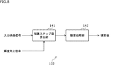
- FIG. 8 shows an example of a method for measuring the amount of temperature rise by the temperature rise amount measuring unit 132.
- the temperature rise amount measuring unit 132 includes an integration step value calculation unit 141 and an integration processing unit 142.
- the input video signal and the luminance improvement magnification are input to the integration step value calculation unit 141.
- the integration step value calculation unit 141 calculates the step value when performing the integration process according to the load increased by the brightness enhancement process.
- the positive integration step value in the high load state is made larger than the predetermined value according to the temperature that suddenly rises in the high load state, and the load is lower than the high load state.
- the negative integration step value in the low load state is set to be smaller than the predetermined value according to the temperature that slowly decreases in the load state.
- FIG. 9 the relationship between the load increase amount and the integration step value when the horizontal axis is the load increase amount and the vertical axis is the integration step is shown by a thick line L51.
- the integration processing unit 142 integrates the integration step values in the time axis direction and calculates an integration value that correlates with the temperature rise.
- FIG. 10 shows the relationship between the load increase amount and the integrated value by the thick line L61 and the thick line L62 on the same time axis. That is, FIG. 10 shows the state of integration in consideration of the temperature increase, and the integrated value represents the amount of temperature increase accompanying the increase in brightness.
- these processes are executed for each predetermined area on the screen of the display panel, and the integrated value for each predetermined area is calculated, so that the high brightness processing is performed at the same location ( It is possible to detect a state in which the temperature is rising by concentrating on the region) in a short period of time.
- the area on the screen of the display panel can be, for example, an area of the entire screen divided into a plurality of areas having predetermined sizes in the vertical direction and the horizontal direction. Specifically, it can be an area corresponding to the division area A of FIG. 12, which will be described later.
- the load of the image is predicted by signal processing, or the actual surface temperature of the display panel is measured by a temperature sensor or the like, and the temperature information obtained there is obtained for each predetermined area on the screen of the display panel.
- the accuracy can be further improved.
- Only one temperature sensor may be attached to the panel portion 113 as supplementary information for load prediction by signal processing, or a panel for the purpose of improving the accuracy of supplementary information or directly measuring without load prediction by signal processing. A plurality of them may be attached to the portion 113.
- FIG. 11 shows a configuration example of one temperature sensor provided on the panel unit 113.
- the temperature sensor 171 is attached at a position corresponding to a substantially central portion of the screen of the display panel, and measures the surface temperature of the display panel.
- the temperature sensor 171 is not limited to the position corresponding to the substantially central portion of the screen, and may be attached to another position.
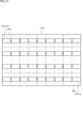
- FIG. 12 shows a configuration example of a plurality of temperature sensors provided on the panel unit 113.
- FIG. 12 shows an example in which the entire screen area of the display panel is divided into 4 ⁇ 9 areas having the same size in the vertical direction and the horizontal direction, and the temperature sensor 171 is attached to each divided area. ing. For convenience of explanation, a broken line indicating the boundary of the divided area is described on the screen of the display panel.
- the numbers corresponding to the vertical direction and the horizontal direction of the divided area A are described in the upper left divided area A11 and the lower right divided area Aij on the screen of the display panel. Further, the numbers corresponding to the vertical direction and the horizontal direction of the temperature sensor 171 are described in the temperature sensor 171-11 on the upper left and the temperature sensor 171-ij on the lower right.
- i represents a vertical number and j represents a horizontal number. That is, in FIG. 12, an example in which the screen of the display panel is divided into 4 ⁇ 9 divided areas is shown, but it is possible to divide the screen into i ⁇ j (integer of i, j: 1 or more) divided area A.
- the number of division regions A to which the temperature sensor 171 is attached is arbitrary.
- the temperature sensor 171-11 measures the surface temperature of the divided region A11 in the screen of the display panel. Since it will be repeated, the description thereof will be omitted, but the surface temperature of the divided region Aij corresponding to the mounting position is similarly measured for the temperature sensors 171-ij other than the temperature sensors 171-11.
- the temperature sensor 171 in FIG. 11 and the temperature sensors 171-11 to 171-ij in FIG. 12 correspond to the panel temperature measurement unit 151 in FIG.
- the surface temperature of the display panel can be measured more accurately than when one temperature sensor 171 is attached.
- APL Average Picture Level
- APL Average Picture Level
- the high APL state represents a state in which the APL value is higher than a predetermined value, that is, a state in which the signal level of the video signal is high.
- the low APL state represents a state in which the APL value is lower than a predetermined value, that is, a state in which the signal level of the video signal is low.
- FIG. 13 shows an example of a video signal that is greatly affected by the temperature rise.
- FIG. 13A shows a case where the entire screen of the display panel becomes an image corresponding to the image signal in a state where the signal level is high.
- FIG. 13B shows a case where the local region (white region in the figure) in the substantially central portion of the screen of the display panel becomes an image corresponding to the image signal in a state where the signal level is high.
- the APL measurement unit 133 measures the APL of the entire screen of the display panel or each predetermined area.
- the area on the screen of the display panel can be, for example, an area of the entire screen divided into a plurality of areas having predetermined sizes in the vertical direction and the horizontal direction. Specifically, it can be a region corresponding to the division region A in FIG. 12 described above.
- the OLED display panel has a different current load for the lighting amount of each pixel (OLED element) arranged two-dimensionally. If the amount of load increase due to the high brightness processing is calculated only by the above-mentioned APL measurement, it is difficult to consider the difference between these current loads. Therefore, the accuracy can be expected to be improved by measuring the current flowing through the OLED display panel with a current sensor or the like.
- the brightness improvement gain calculation unit 134 uses the APL. It suffices if the control is performed so as to relax the suppression of the luminance improvement gain according to the measurement result of.
- FIG. 14 shows the relationship between the color component of each pixel and the current value.
- the horizontal axis represents the color of the sub-pixel (White, Red, Green, Blue) and the color when the sub-pixel is lit in two colors (Yellow, Cyan, Magenta), and the vertical axis represents the panel drive current value. Shown. In each pixel, when the sub-pixels R and G are lit, the color becomes yellow (Y), when the sub-pixels R and B are lit, the color becomes magenta (M), and when the sub-pixels G and B are lit, the color becomes cyan (C). )become.
- the brightness improvement gain calculation unit 134 improves the brightness of the display panel by controlling the brightness improvement gain according to the degree of influence of the temperature rise of each element (brightness improvement time, temperature rise amount, APL, current load). When doing so, the temperature rise of the display panel is suppressed. Examples of gain setting for each element are shown in FIGS. 15 to 17.
- FIG. 15 shows an example of setting the gain with respect to the brightness improvement time.
- the horizontal axis represents the brightness improvement time (integrated value), and the vertical axis represents the brightness improvement time interlocking gain.
- the gain according to the brightness improvement time is indicated by a thick line L81 including a straight line descending to the right, and the brightness improvement time interlocking gain is maintained at 100% until the integrated value reaches a predetermined value.
- the integrated value exceeds the predetermined value, it gradually decreases with a predetermined slope, and after it decreases to 0%, it continues to be 0% as it is.
- FIG. 16 shows an example of setting the gain with respect to the amount of temperature rise.
- the horizontal axis represents the amount of temperature rise (integrated value), and the vertical axis represents the gain linked to the amount of temperature rise.
- the gain according to the amount of temperature rise is indicated by a thick line L82 including a straight line falling to the right, and the gain of this amount of temperature rise is maintained at 100% until the integrated value reaches a predetermined value. , After the integrated value exceeds the predetermined value, it gradually decreases with a predetermined slope, and after it decreases to 0%, it continues to be 0% as it is.
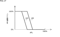
- FIG. 17 shows an example of gain setting for APL.
- the horizontal axis represents APL and the vertical axis represents APL-linked gain.
- the value of APL on the horizontal axis is a value in the range of 0% to 100%.
- the gain corresponding to the APL is indicated by thick lines L83 and L84 including a straight line descending to the right.
- the thick line L83 shows the APL interlocking gain when the measured amount of the current load is high
- the thick line L84 shows the APL interlocking gain when the measured amount of the current load is low.
- the APL interlocking gain is maintained at 100% until the APL value reaches the predetermined value, but gradually decreases with a predetermined slope after the APL value exceeds the predetermined value. After decreasing to 0%, continue 0% as it is.
- the thick wire L83 has a smaller APL value until the APL interlocking gain decreases than the thick wire L84, and when the measured amount of the current load is high, the APL interlocking gain decreases with a smaller APL value. become.
- the APL interlocking gain may be set according to the APL without considering the current load.
- such interlocking gains are set, and for example, a value obtained by multiplying these interlocking gain values, a minimum value among these interlocking gain values, and the like are finally used for brightness improvement. Set as gain.
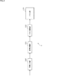
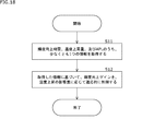
- FIG. 18 is a flowchart illustrating the flow of the luminance improvement gain control process executed by the signal processing unit 111.
- step S11 the luminance improvement gain calculation unit 134 acquires at least one piece of information among the luminance improvement time measurement result, the temperature rise amount measurement result, and the APL measurement result.
- the measurement result of the current flowing through the display panel may be acquired.
- step S12 the brightness improvement gain calculation unit 134 adaptively controls the brightness improvement gain according to the degree of influence of the temperature rise based on the acquired information.
- the value obtained by multiplying the gain is set as the final brightness improvement gain.
- the brightness improvement time and the display panel are measured by measuring the time for improving the brightness in the display panel.
- the brightness improvement gain is affected by the temperature rise of the display panel based on at least one information of the short-term temperature rise amount of the above and the feature amount (for example, APL) of the video signal according to the image displayed on the display panel. It is controlled adaptively while estimating the degree.
- the signal processing unit 111 has been described as a component of the display device 1, but the signal processing unit 111 may be regarded as a single device and may be a signal processing device.
- the display device 1 is a television receiver
- a device such as a display device may be used.
- the display device includes, for example, a monitor for medical use, a monitor for broadcasting, a display for digital signage, and the like.
- the display device 1 can be used as a PC (Personal Computer), a tablet terminal, a smartphone, a mobile phone, a game machine, a head-mounted display, an in-vehicle device such as a car navigation system or a monitor for a rear seat, a wearable device such as a wristwatch type or a glasses type, and the like. It may be used as a display unit of.
- PC Personal Computer
- tablet terminal a smartphone
- a mobile phone such as a game machine
- a head-mounted display such as a car navigation system or a monitor for a rear seat
- a wearable device such as a wristwatch type or a glasses type, and the like. It may be used as a display unit of.
- the display device 1 is an example of an OLED display device having an OLED display panel, but the present technology can also be applied to a display device such as a self-luminous display device having another self-luminous display panel. be.
- each pixel arranged two-dimensionally on the panel unit 113 is composed of four sub-pixels of white (W), red (R), green (G), and blue (B).
- W white
- R red
- G green
- B blue
- the color of the sub-pixel is not limited to these.
- a sub-pixel of another color having the same high visual sensitivity as the white (W) may be used.
- OLED may be read as “organic EL (Electro Luminescence)".
- OLED display device can be said to be an organic EL display device.
- video since the video is composed of a plurality of image frames, "video” may be read as "image”.
- a signal processing device including a signal processing unit that adaptively controls a first gain for improving the brightness of the video signal based on the acquired information according to the degree of influence of a temperature rise on the display panel.
- the signal processing unit additionally adds the first gain to the second gain used for increasing the brightness, thereby realizing the increase in brightness of the video signal (1). Or the signal processing device according to (2).
- the signal processing unit uses a value corresponding to the interlocking gain linked to at least one information of the brightness improvement time, the temperature rise amount, and the feature amount as the first gain (1) to (3). ).
- the signal processing device according to any one of. (5)
- the signal processing unit uses a value obtained by multiplying the plurality of interlocking gain values or a minimum value among the plurality of interlocking gain values as the first gain.
- the signal processing unit Calculate the integration step value according to the level of the video signal, The signal processing device according to any one of (1) to (5) above, wherein the calculated integrated step value is integrated in the time axis direction to calculate the integrated value according to the brightness improvement time. (7) The signal processing device according to (6), wherein the signal processing unit calculates an integrated value according to the brightness improvement time for each predetermined area on the screen of the display panel. (8) The signal processing unit Calculate the integration step value when performing integration according to the load that increases due to the increase in brightness. The signal processing apparatus according to any one of (1) to (7) above, wherein the calculated integrated step values are integrated in the time axis direction to calculate the integrated value according to the temperature rise.
- the signal processing unit sets a positive integration step value corresponding to the high load state to be larger than a predetermined value, and sets the load to a low load state lower than the high load state.
- the signal processing apparatus according to (8) above, wherein the corresponding negative integration step value is set to be smaller than a predetermined value.
- the signal processing device according to (8) or (9), wherein the signal processing unit calculates an integrated value according to the temperature rise for each predetermined area on the screen of the display panel.
- the signal processing unit adds information on the temperature obtained by predicting the load of the image or measuring the temperature sensor provided on the display panel to the integrated value according to the temperature rise (8) to (10).
- the signal processing apparatus according to any one of.
- the signal processing device (12) The signal processing device according to (11), wherein one or a plurality of temperature sensors for measuring the surface temperature are provided on the display panel. (13) The signal processing device according to any one of (1) to (12) above, wherein the feature amount is APL. (14) The signal processing device according to (13), wherein the signal processing unit measures the APL for the entire screen of the display panel or for each predetermined area on the screen. (15) The signal processing device according to (4), wherein the signal processing unit adds the measurement result of the current flowing through the display panel to the interlocking gain linked to the feature amount.
- the signal processing device When the video signal is increased in brightness from a low-luminance display signal to a high-luminance display signal, the brightness improvement time measured by measuring the time for improving the brightness in the display panel, the amount of temperature rise in the display panel, and the display panel Acquire at least one piece of information among the feature quantities of the video signal according to the displayed video, A signal processing method that adaptively controls a first gain for improving the brightness of the video signal based on the acquired information according to the degree of influence of a temperature rise on the display panel. (17) A signal processing unit that processes video signals and A panel unit having a display panel for displaying an image corresponding to the image signal is provided.
- the signal processing unit When the video signal is increased in brightness from a low-luminance display signal to a high-luminance display signal, the brightness improvement time measured by measuring the time for improving the brightness in the display panel, the amount of temperature rise in the display panel, and the display. Acquire at least one piece of information among the feature quantities of the video signal corresponding to the video displayed on the panel.
- a display device that adaptively controls a first gain for improving the brightness of the video signal based on the acquired information according to the degree of influence of a temperature rise on the display panel.
- Display device 110 signal input unit, 111 signal processing unit, 112 panel drive unit, 113 panel unit, 131 brightness improvement time measurement unit, 132 temperature rise measurement unit, 133 APL measurement unit, 134 brightness improvement gain calculation unit, 135 Addition unit, 136 multiplication unit, 151 panel temperature measurement unit, 152 panel current measurement unit, 171 temperature sensor
Landscapes
- Engineering & Computer Science (AREA)
- Physics & Mathematics (AREA)
- Computer Hardware Design (AREA)
- General Physics & Mathematics (AREA)
- Theoretical Computer Science (AREA)
- Control Of Indicators Other Than Cathode Ray Tubes (AREA)
- Electroluminescent Light Sources (AREA)
- Control Of El Displays (AREA)
Priority Applications (4)
| Application Number | Priority Date | Filing Date | Title |
|---|---|---|---|
| US17/919,068 US12531014B2 (en) | 2020-05-01 | 2021-04-19 | Signal processing device, signal processing method, and display device |
| EP21796972.4A EP4145435A4 (en) | 2020-05-01 | 2021-04-19 | SIGNAL PROCESSING DEVICE, SIGNAL PROCESSING METHOD AND DISPLAY DEVICE |
| JP2022517639A JPWO2021220853A1 (https=) | 2020-05-01 | 2021-04-19 | |
| CN202180030608.7A CN115443498A (zh) | 2020-05-01 | 2021-04-19 | 信号处理装置、信号处理方法及显示装置 |
Applications Claiming Priority (2)
| Application Number | Priority Date | Filing Date | Title |
|---|---|---|---|
| JP2020-081150 | 2020-05-01 | ||
| JP2020081150 | 2020-05-01 |
Publications (1)
| Publication Number | Publication Date |
|---|---|
| WO2021220853A1 true WO2021220853A1 (ja) | 2021-11-04 |
Family
ID=78374089
Family Applications (1)
| Application Number | Title | Priority Date | Filing Date |
|---|---|---|---|
| PCT/JP2021/015795 Ceased WO2021220853A1 (ja) | 2020-05-01 | 2021-04-19 | 信号処理装置、信号処理方法、及び表示装置 |
Country Status (5)
| Country | Link |
|---|---|
| US (1) | US12531014B2 (https=) |
| EP (1) | EP4145435A4 (https=) |
| JP (1) | JPWO2021220853A1 (https=) |
| CN (1) | CN115443498A (https=) |
| WO (1) | WO2021220853A1 (https=) |
Cited By (1)
| Publication number | Priority date | Publication date | Assignee | Title |
|---|---|---|---|---|
| EP4184493A3 (en) * | 2021-11-19 | 2023-08-09 | Samsung Display Co., Ltd. | Display device |
Families Citing this family (1)
| Publication number | Priority date | Publication date | Assignee | Title |
|---|---|---|---|---|
| KR20240002281A (ko) * | 2022-06-28 | 2024-01-05 | 삼성디스플레이 주식회사 | 표시 장치 및 그 구동 방법 |
Citations (4)
| Publication number | Priority date | Publication date | Assignee | Title |
|---|---|---|---|---|
| JP2003316320A (ja) * | 2002-04-24 | 2003-11-07 | Sanyo Electric Co Ltd | 表示装置 |
| JP2015094795A (ja) | 2013-11-11 | 2015-05-18 | ソニー株式会社 | 信号生成装置、信号生成プログラム、信号生成方法、及び、画像表示装置 |
| JP2015125356A (ja) * | 2013-12-27 | 2015-07-06 | 株式会社Joled | 表示装置、駆動方法および電子機器 |
| US20170162098A1 (en) * | 2015-12-08 | 2017-06-08 | Samsung Display Co., Ltd. | Organic light emitting display device and method of driving the same |
Family Cites Families (10)
| Publication number | Priority date | Publication date | Assignee | Title |
|---|---|---|---|---|
| BE1007478A3 (nl) * | 1993-09-07 | 1995-07-11 | Philips Electronics Nv | Weergeefinrichting met temperatuurcompensatie. |
| US7804470B2 (en) | 2007-03-23 | 2010-09-28 | Seiko Epson Corporation | Temperature adaptive overdrive method, system and apparatus |
| CN101609629A (zh) * | 2009-03-20 | 2009-12-23 | 北京中庆微数字设备开发有限公司 | 一种自动温控的发光指示牌 |
| KR20110096930A (ko) * | 2010-02-24 | 2011-08-31 | (주)지에스디 | 고휘도 모니터 자동 온도제어 시스템 |
| JP2015049399A (ja) * | 2013-09-02 | 2015-03-16 | 凸版印刷株式会社 | 表示制御装置 |
| CN107851417B (zh) * | 2015-07-30 | 2021-06-11 | 索尼公司 | 显示控制装置和显示控制方法 |
| KR102412107B1 (ko) * | 2015-10-29 | 2022-06-24 | 엘지디스플레이 주식회사 | 휘도 제어장치와 이를 포함하는 표시장치 |
| JP6656265B2 (ja) * | 2015-12-14 | 2020-03-04 | シャープ株式会社 | 表示装置およびその駆動方法 |
| CN107256688B (zh) * | 2016-04-22 | 2020-04-21 | 长春希达电子技术有限公司 | 一种亮度自适应的led显示屏温度控制系统 |
| CN107610676A (zh) * | 2017-09-27 | 2018-01-19 | 上海展扬通信技术有限公司 | 一种智能终端的屏幕亮度控制方法及屏幕亮度控制系统 |
-
2021
- 2021-04-19 EP EP21796972.4A patent/EP4145435A4/en active Pending
- 2021-04-19 JP JP2022517639A patent/JPWO2021220853A1/ja active Pending
- 2021-04-19 US US17/919,068 patent/US12531014B2/en active Active
- 2021-04-19 WO PCT/JP2021/015795 patent/WO2021220853A1/ja not_active Ceased
- 2021-04-19 CN CN202180030608.7A patent/CN115443498A/zh active Pending
Patent Citations (4)
| Publication number | Priority date | Publication date | Assignee | Title |
|---|---|---|---|---|
| JP2003316320A (ja) * | 2002-04-24 | 2003-11-07 | Sanyo Electric Co Ltd | 表示装置 |
| JP2015094795A (ja) | 2013-11-11 | 2015-05-18 | ソニー株式会社 | 信号生成装置、信号生成プログラム、信号生成方法、及び、画像表示装置 |
| JP2015125356A (ja) * | 2013-12-27 | 2015-07-06 | 株式会社Joled | 表示装置、駆動方法および電子機器 |
| US20170162098A1 (en) * | 2015-12-08 | 2017-06-08 | Samsung Display Co., Ltd. | Organic light emitting display device and method of driving the same |
Non-Patent Citations (1)
| Title |
|---|
| See also references of EP4145435A4 |
Cited By (1)
| Publication number | Priority date | Publication date | Assignee | Title |
|---|---|---|---|---|
| EP4184493A3 (en) * | 2021-11-19 | 2023-08-09 | Samsung Display Co., Ltd. | Display device |
Also Published As
| Publication number | Publication date |
|---|---|
| CN115443498A (zh) | 2022-12-06 |
| EP4145435A4 (en) | 2023-10-25 |
| US12531014B2 (en) | 2026-01-20 |
| JPWO2021220853A1 (https=) | 2021-11-04 |
| US20230162668A1 (en) | 2023-05-25 |
| EP4145435A1 (en) | 2023-03-08 |
Similar Documents
| Publication | Publication Date | Title |
|---|---|---|
| US11056050B2 (en) | Display unit, image processing unit, and display method for improving image quality | |
| US8743152B2 (en) | Display apparatus, method of driving display apparatus, drive-use integrated circuit, driving method employed by drive-use integrated circuit, and signal processing method | |
| JP6614859B2 (ja) | 表示装置、表示装置の制御方法、画像処理装置、プログラム、及び、記録媒体 | |
| KR102659203B1 (ko) | 표시 장치, 및 신호 처리 장치 | |
| KR102154698B1 (ko) | 표시장치와 그 휘도 향상 방법 | |
| CN110459176A (zh) | 一种amoled显示器的色域转换方法 | |
| KR20170109356A (ko) | 유기 발광 다이오드 표시 장치 및 그의 동작 방법 | |
| US9830882B2 (en) | Display device and color conversion method | |
| WO2021131830A1 (ja) | 信号処理装置、信号処理方法、及び表示装置 | |
| JP2007122013A (ja) | 表示画像補正装置、画像表示装置、表示画像補正方法 | |
| WO2021220853A1 (ja) | 信号処理装置、信号処理方法、及び表示装置 | |
| US12236857B2 (en) | Signal processing apparatus, signal processing method, and display apparatus | |
| KR20220030509A (ko) | 표시 장치 및 표시 장치의 휘도 보상 방법 | |
| KR100753318B1 (ko) | 표시 장치 | |
| US12505792B2 (en) | Signal processing apparatus, signal processing method, and display apparatus | |
| US7808459B2 (en) | Light emitting display device | |
| JP2006308685A (ja) | 表示装置 | |
| US12620342B2 (en) | Display apparatus for reducing an effect of cross-talk and method for controlling same |
Legal Events
| Date | Code | Title | Description |
|---|---|---|---|
| 121 | Ep: the epo has been informed by wipo that ep was designated in this application |
Ref document number: 21796972 Country of ref document: EP Kind code of ref document: A1 |
|
| ENP | Entry into the national phase |
Ref document number: 2022517639 Country of ref document: JP Kind code of ref document: A |
|
| ENP | Entry into the national phase |
Ref document number: 2021796972 Country of ref document: EP Effective date: 20221201 |
|
| NENP | Non-entry into the national phase |
Ref country code: DE |
|
| WWG | Wipo information: grant in national office |
Ref document number: 17919068 Country of ref document: US |