WO2021214865A1 - 波長可変光フィルタ - Google Patents
波長可変光フィルタ Download PDFInfo
- Publication number
- WO2021214865A1 WO2021214865A1 PCT/JP2020/017176 JP2020017176W WO2021214865A1 WO 2021214865 A1 WO2021214865 A1 WO 2021214865A1 JP 2020017176 W JP2020017176 W JP 2020017176W WO 2021214865 A1 WO2021214865 A1 WO 2021214865A1
- Authority
- WO
- WIPO (PCT)
- Prior art keywords
- optical filter
- incident surface
- tunable optical
- transparent electrode
- component
- Prior art date
- Legal status (The legal status is an assumption and is not a legal conclusion. Google has not performed a legal analysis and makes no representation as to the accuracy of the status listed.)
- Ceased
Links
Images

Classifications
-
- G—PHYSICS
- G02—OPTICS
- G02B—OPTICAL ELEMENTS, SYSTEMS OR APPARATUS
- G02B26/00—Optical devices or arrangements for the control of light using movable or deformable optical elements
- G02B26/002—Optical devices or arrangements for the control of light using movable or deformable optical elements the movement or the deformation controlling the frequency of light, e.g. by Doppler effect
-
- G—PHYSICS
- G02—OPTICS
- G02B—OPTICAL ELEMENTS, SYSTEMS OR APPARATUS
- G02B26/00—Optical devices or arrangements for the control of light using movable or deformable optical elements
-
- G—PHYSICS
- G02—OPTICS
- G02B—OPTICAL ELEMENTS, SYSTEMS OR APPARATUS
- G02B26/00—Optical devices or arrangements for the control of light using movable or deformable optical elements
- G02B26/001—Optical devices or arrangements for the control of light using movable or deformable optical elements based on interference in an adjustable optical cavity
-
- G—PHYSICS
- G02—OPTICS
- G02B—OPTICAL ELEMENTS, SYSTEMS OR APPARATUS
- G02B26/00—Optical devices or arrangements for the control of light using movable or deformable optical elements
- G02B26/007—Optical devices or arrangements for the control of light using movable or deformable optical elements the movable or deformable optical element controlling the colour, i.e. a spectral characteristic, of the light
-
- G—PHYSICS
- G02—OPTICS
- G02F—OPTICAL DEVICES OR ARRANGEMENTS FOR THE CONTROL OF LIGHT BY MODIFICATION OF THE OPTICAL PROPERTIES OF THE MEDIA OF THE ELEMENTS INVOLVED THEREIN; NON-LINEAR OPTICS; FREQUENCY-CHANGING OF LIGHT; OPTICAL LOGIC ELEMENTS; OPTICAL ANALOGUE/DIGITAL CONVERTERS
- G02F1/00—Devices or arrangements for the control of the intensity, colour, phase, polarisation or direction of light arriving from an independent light source, e.g. switching, gating or modulating; Non-linear optics
- G02F1/01—Devices or arrangements for the control of the intensity, colour, phase, polarisation or direction of light arriving from an independent light source, e.g. switching, gating or modulating; Non-linear optics for the control of the intensity, phase, polarisation or colour
- G02F1/03—Devices or arrangements for the control of the intensity, colour, phase, polarisation or direction of light arriving from an independent light source, e.g. switching, gating or modulating; Non-linear optics for the control of the intensity, phase, polarisation or colour based on ceramics or electro-optical crystals, e.g. exhibiting Pockels effect or Kerr effect
Definitions
- the present invention relates to a Fabry-Perot interferometer type tunable optical filter.
- Wavelength Division Multiplexing is one of the technologies that realizes large-capacity transmission of optical communication.
- a plurality of optical signals having different wavelengths, a combiner that combines the plurality of optical signals, an optical fiber for long-distance transmission, and the combined optical signal are demultiplexed (the combined optical signal is demultiplexed).
- It is composed of a demultiplexer composed of a wavelength-variable optical filter for (separating wavelengths) and a photoreceiver that photoelectrically converts (receives) the demultiplexed optical signal.
- the demultiplexer needs to finely demultiplex a plurality of wavelengths on the sub-nm order. Furthermore, by increasing the speed of the demultiplexer, further increase in capacity can be expected. Further, a tunable optical filter is required not only for communication applications but also for controlling the oscillation wavelength of a laser.
- diffraction grating type and acoustic optical type have been proposed as tunable light filters. Since the wavelength width that can be decomposed by these conventional tunable optical filters is as large as nm, a Fabry-Perot interferometer type filter that can decompose wavelengths more finely has also been proposed.
- the Fabry-Perot interferometer type wavelength variable optical filter changes the extracted wavelength by changing the length between the two partially reflecting surfaces, but the length between the two partially reflecting surfaces is mechanical. Therefore, there is a problem that the operating speed is limited to the kHz order.
- a tunable optical filter using a KTN crystal has also been proposed (see Patent Document 1). By applying an electric field, the KTN crystal can obtain crystal strain depending on the magnitude of the electric field. By using a KTN crystal having such an electrostrictive effect, the length between the two partially reflecting surfaces can be changed.
- the Fabry-Perot interferometer type tunable optical filter described above utilizes the fact that the crystal to which an electric field is applied causes distortion (electrostraining effect).
- the length between the two partially reflecting surfaces can be changed at high speed, and it can function as a tunable optical filter.
- an electrode is provided on the crystal and a voltage is applied from the outside. Since the electric field is defined by the drive voltage / the distance between the electrodes, it is important that the distance between the electrodes is short in order to operate with a small drive voltage.
- electrodes are formed on each of two parallel surfaces sandwiching the optical axis passing through the partial reflection surface formed on the exit surface of the KTN crystal.
- the width of the partially reflecting surface needs to be larger than the beam diameter. Therefore, the distance between two parallel planes of the KTN crystal that sandwich the optical axis is wider than the beam diameter. In other words, the distance between the two electrodes described above is larger than the beam diameter.
- the beam diameter of the light propagating inside the Fabry-Perot interferometer type should be reduced. Is important. However, when a beam of light is formed using a generally available optical system, the beam diameter is limited to several mm at the smallest.
- the required drive voltage is 200 V when the distance between the electrodes is 0.5 mm.
- the distance between the electrodes spreads to 3 mm, and a driving voltage of 1200 V is required to obtain the same amount of distortion as described above.
- the need for a high drive voltage has the problem that the system is not only expensive but also complicated.
- the present invention has been made to solve the above problems, and an object of the present invention is to enable a Fabry-Perot interferometer-type tunable optical filter to be driven with a lower drive voltage.
- the variable wavelength optical filter according to the present invention includes a first incident surface and a first exit surface arranged on the opposite side of the first incident surface, and is made of a material having an electrolytic distortion effect and transmitting light. It includes a plate-shaped first component in which the first incident surface and the first exit surface are arranged on the optical axis, and a second exit surface arranged on the side opposite to the second incident surface and the second incident surface.
- a plate-like material composed of a material that allows light to pass through, the second incident surface and the second exit surface are arranged on the optical axis, and the distance between the first incident surface and the second incident surface is constant on the optical axis.
- a second transparent electrode formed between the two, and a second reflective film formed on the second incident surface and partially reflecting light are provided, and the first reflective film and the second reflective film interfere with the fabric perow. The total is configured.
- the driving voltage is lower.
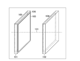
- FIG. 1 is a cross-sectional view showing a configuration of a tunable optical filter according to an embodiment of the present invention.
- FIG. 2 is a perspective view showing a configuration of a tunable optical filter according to an embodiment of the present invention.
- This tunable optical filter includes a plate-shaped first component 101, a plate-shaped second component 102, a first reflective film 103, a second reflective film 104, a first transparent electrode 105, and a second transparent electrode. It includes 106.
- the first component 101 includes a first incident surface 101a and a first exit surface 101b arranged on the opposite side of the first incident surface 101a. Further, the first component 101 is made of a material having an electrostrictive effect and transmitting light. The first component 101 can be composed of, for example, a piezoelectric crystal having an electrostrictive effect. The first component 101 is made of a material having high transparency to light in the target wavelength band.
- the first component 101 is, for example, a KTN [KTa 1- ⁇ Nb ⁇ O 3 (0 ⁇ ⁇ 1)] crystal or a lithium-added KLTN [K 1- ⁇ Li ⁇ Ta 1- ⁇ Nb ⁇ O 3 ( It can be composed of any of 0 ⁇ ⁇ 1,0 ⁇ ⁇ 1)] crystals.
- KTN crystals and KLTN crystals are known as crystals having an electrostrictive effect. It is known that the electric strain effect of these crystals can obtain a strain amount proportional to the square of the electric field defined by the voltage / distance between electrodes.
- the first component 101 can also be composed of barium titanate (BaTIO 3 ), lithium niobate (LiNbO 3 ), calcium fluoride (CaF 2) and the like.
- the first component 101 is required to have a surface accuracy (maximum shape error) of the first incident surface 101a and the first exit surface 101b of about the wavelength of the target light / 10.
- the second component 102 includes a second incident surface 102a and a second exit surface 102b arranged on the side opposite to the second incident surface 102a. Further, the second component 102 is made of a material through which light is transmitted. The second component 102 can be made of a material having high transparency to light in the target wavelength band. The second component 102 can be made of, for example, BK7 glass or quartz glass. The second component 102 includes KTN [KTa 1- ⁇ Nb ⁇ O 3 (0 ⁇ ⁇ 1)] crystals or lithium-added KLTN [K 1- ⁇ Li ⁇ Ta 1- ⁇ Nb ⁇ O 3 ( It can also be composed of any of 0 ⁇ ⁇ 1,0 ⁇ ⁇ 1)] crystals.
- the second component 102 can also be composed of barium titanate (BaTIO 3 ), lithium niobate (LiNbO 3 ), calcium fluoride (CaF 2) and the like.
- the second component 102 is required to have a surface accuracy (maximum shape error) of the second incident surface 102a and the second exit surface 102b of about the wavelength of the target light / 10.
- the first incident surface 101a and the first exit surface 101b of the first component 101 are arranged on the optical axis (optical path) 131, and both the second incident surface 102a and the second exit surface 102b of the second component 102 It is arranged on the optical axis 131. Further, the distance between the first incident surface 101a and the second incident surface 102a is constant on the optical axis 131. For example, if the first component 101 and the second component 102 are fixedly arranged on a surface plate (not shown), the distance between the first incident surface 101a and the second incident surface 102a can be fixed on the optical axis 131. can.
- variable wavelength optical filter is formed on the first reflecting film 103 that partially reflects light formed on the first emitting surface 101b and the second incident surface 102a that partially reflects light.
- a second reflective film 104 that reflects light is provided.
- the Fabry-Perot interferometer is composed of the first reflective film 103 and the second reflective film 104.
- first exit surface 101b and the second incident surface 102a can be arranged so as to face each other and have a parallel relationship with each other. Further, the first incident surface 101a and the first exit surface 101b can be in a parallel relationship with each other. Similarly, the second incident surface 102a and the second exit surface 102b can be in a parallel relationship with each other.
- the first exit surface 101b and the second incident surface 102a face each other. There is no need to place the position.
- the first exit surface 101b and the second incident surface 102a can be planes perpendicular to the optical axis 131.
- the positional relationship between the first exit surface 101b and the second incident surface 102a described above is synonymous with the relationship between the reflection surface of the first reflection film 103 and the reflection surface of the second reflection film 104.
- the wavelength tunable optical filter according to the embodiment has a second transparent electrode 105 formed on the first incident surface 101a, and a second transparent electrode 105 formed between the first exit surface 101b and the first reflective film 103. It includes an electrode 106.
- the first transparent electrode 105 and the second transparent electrode 106 can be made of, for example, indium tin oxide (ITO). Further, the distance between the first transparent electrode 105 and the second transparent electrode 106, in other words, the plate thickness of the first component 101 is smaller than the beam diameter of light.
- the distance (interval) between the first transparent electrode 105 and the second transparent electrode 106 is 0.1 mm, the reflective surface of the first reflective film 103 and the second reflective film 104.
- the distance from the reflecting surface (distance on the optical axis) is 10 ⁇ m, and the reflectance of the first reflecting film 103 and the second reflecting film 104 can be 99.5%.
- variable wavelength optical filter Due to this change in the amount of strain, the distance (distance on the optical axis) between the reflective surface of the first reflective film 103 and the reflective surface of the second reflective film 104 changes. Due to this change, the variable wavelength optical filter according to the Fabry-Perot interferometer type embodiment has a filter width of 0.2 nm with respect to a wavelength in the 1550 nm band, and enables sweeping at a wavelength of 100 nm.
- the second transparent electrode 106 and the first reflective film 103 are arranged on the first exit surface 101b of the first component 101. Therefore, the distance between the first transparent electrode 105 and the second transparent electrode 106 is determined by the plate thickness of the first component 101, and is the area of the first incident surface 101a and the first exit surface 101b through which the light beam passes. Not involved in.
- the distance between the electrodes is not limited by the beam diameter. According to the embodiment, it is possible to design a design in which the distance between the electrodes is short, and it is possible to reduce the required drive voltage.
- the distance (plate thickness) through which light passes through the first component 101 is short (thin). If the thickness of the component to which the electrode is provided is reduced in the light transmission direction, the installation area of the electrode becomes small and it becomes difficult to install the electrode. For example, if the thickness in the light transmission direction is 0.1 mm, conventionally, electrodes cannot be installed, and it becomes difficult to operate as a tunable light filter.
- the KTN crystal and the KLTN crystal have the largest strain amount in the same direction as the electric field direction.
- the direction in which the first component 101 is desired to be distorted (expanded / contracted) is the direction of the optical axis 131, in other words, the plate thickness direction of the first component 101, which is the direction of the electric field and the direction of water viewing.
- the required amount of strain in the first component 101 can be obtained at a lower voltage.
- the drive is lower.
- the voltage can drive a Fabry-Perot interferometer-type variable wavelength optical filter.
Landscapes
- Physics & Mathematics (AREA)
- General Physics & Mathematics (AREA)
- Optics & Photonics (AREA)
- Spectroscopy & Molecular Physics (AREA)
- Astronomy & Astrophysics (AREA)
- Nonlinear Science (AREA)
- Engineering & Computer Science (AREA)
- Ceramic Engineering (AREA)
- Crystallography & Structural Chemistry (AREA)
- Chemical & Material Sciences (AREA)
- Mechanical Light Control Or Optical Switches (AREA)
- Optical Filters (AREA)
- Optical Modulation, Optical Deflection, Nonlinear Optics, Optical Demodulation, Optical Logic Elements (AREA)
- Spectrometry And Color Measurement (AREA)
Abstract
Description
Claims (8)
- 第1入射面と前記第1入射面と反対側に配置された第1出射面とを備え、電歪効果を有して光が透過する材料から構成され、前記第1入射面と前記第1出射面とが光軸上に配置された板状の第1部品と、
第2入射面と前記第2入射面と反対側に配置された第2出射面とを備え、前記光が透過する材料から構成され、前記第2入射面と前記第2出射面とが前記光軸上に配置され、前記光軸上で前記第1入射面と前記第2入射面との距離が一定とされた板状の第2部品と、
前記第1出射面に形成された部分的に前記光を反射する第1反射膜と、
前記第1入射面に形成された第1透明電極と、
前記第1出射面と前記第1反射膜との間に形成された第2透明電極と、
前記第2入射面に形成され、部分的に前記光を反射する第2反射膜と
を備え、
前記第1反射膜と前記第2反射膜とによりファブリペロー干渉計が構成されていることを特徴とする波長可変光フィルタ。 - 請求項1記載の波長可変光フィルタにおいて、
前記第1出射面と前記第2入射面とは、互いに向かい合って配置されていることを特徴とする波長可変光フィルタ。 - 請求項1または2記載の波長可変光フィルタにおいて、
前記第1入射面と前記第1出射面とは、互いに平行であることを特徴とする波長可変光フィルタ。 - 請求項1~3のいずれか1項に記載の波長可変光フィルタにおいて、
前記第2入射面と前記第2出射面とは、互いに平行であることを特徴とする波長可変光フィルタ。 - 請求項1~4のいずれか1項に記載の波長可変光フィルタにおいて、
前記第1透明電極と前記第2透明電極との距離は、前記光のビーム径よりも小さいことを特徴とする波長可変光フィルタ。 - 請求項1~5のいずれか1項に記載の波長可変光フィルタにおいて、
前記第1部品は、KTN[KTa1-αNbαO3(0<α<1)]結晶、またはリチウムを添加したKLTN[K1-βLiβTa1-αNbαO3(0<α<1,0<β<1)]結晶のいずれかから構成されていることを特徴とする波長可変光フィルタ。 - 請求項1~6のいずれか1項に記載の波長可変光フィルタにおいて、
前記第2部品は、KTN[KTa1-αNbαO3(0<α<1)]結晶、またはリチウムを添加したKLTN[K1-βLiβTa1-αNbαO3(0<α<1,0<β<1)]結晶のいずれかから構成されていることを特徴とする波長可変光フィルタ。 - 請求項1~7のいずれか1項に記載の波長可変光フィルタにおいて、
前記第1透明電極および前記第2透明電極は、酸化インジウムスズから構成されていることを特徴とする波長可変光フィルタ。
Priority Applications (3)
| Application Number | Priority Date | Filing Date | Title |
|---|---|---|---|
| JP2022516511A JPWO2021214865A1 (ja) | 2020-04-21 | 2020-04-21 | |
| US17/919,959 US12455442B2 (en) | 2020-04-21 | 2020-04-21 | Wavelength variable optical filter |
| PCT/JP2020/017176 WO2021214865A1 (ja) | 2020-04-21 | 2020-04-21 | 波長可変光フィルタ |
Applications Claiming Priority (1)
| Application Number | Priority Date | Filing Date | Title |
|---|---|---|---|
| PCT/JP2020/017176 WO2021214865A1 (ja) | 2020-04-21 | 2020-04-21 | 波長可変光フィルタ |
Publications (1)
| Publication Number | Publication Date |
|---|---|
| WO2021214865A1 true WO2021214865A1 (ja) | 2021-10-28 |
Family
ID=78270422
Family Applications (1)
| Application Number | Title | Priority Date | Filing Date |
|---|---|---|---|
| PCT/JP2020/017176 Ceased WO2021214865A1 (ja) | 2020-04-21 | 2020-04-21 | 波長可変光フィルタ |
Country Status (3)
| Country | Link |
|---|---|
| US (1) | US12455442B2 (ja) |
| JP (1) | JPWO2021214865A1 (ja) |
| WO (1) | WO2021214865A1 (ja) |
Cited By (1)
| Publication number | Priority date | Publication date | Assignee | Title |
|---|---|---|---|---|
| WO2023105565A1 (ja) * | 2021-12-06 | 2023-06-15 | 日本電信電話株式会社 | マイクロダイアフラムポンプ |
Citations (5)
| Publication number | Priority date | Publication date | Assignee | Title |
|---|---|---|---|---|
| JPH09258116A (ja) * | 1996-03-25 | 1997-10-03 | Yazaki Corp | 波長可変フィルタ |
| JP2008145506A (ja) * | 2006-12-06 | 2008-06-26 | Institute Of National Colleges Of Technology Japan | 圧電素子による光学素子とその作成方法 |
| CN101221297A (zh) * | 2008-01-09 | 2008-07-16 | 浙江大学 | 基于pvdf三元共聚物的可调谐光学滤波器 |
| US20090040616A1 (en) * | 2007-08-07 | 2009-02-12 | Xerox Corporation | Fabry-perot piezoelectric tunable filter |
| JP2018085416A (ja) * | 2016-11-22 | 2018-05-31 | 日本電信電話株式会社 | 波長可変ミラーおよび波長可変レーザ |
Family Cites Families (2)
| Publication number | Priority date | Publication date | Assignee | Title |
|---|---|---|---|---|
| JP6467357B2 (ja) | 2016-01-15 | 2019-02-13 | 日本電信電話株式会社 | 波長可変光フィルタ |
| JP7485091B2 (ja) * | 2021-01-13 | 2024-05-16 | 日本電信電話株式会社 | 波長可変光フィルタ |
-
2020
- 2020-04-21 WO PCT/JP2020/017176 patent/WO2021214865A1/ja not_active Ceased
- 2020-04-21 US US17/919,959 patent/US12455442B2/en active Active
- 2020-04-21 JP JP2022516511A patent/JPWO2021214865A1/ja active Pending
Patent Citations (5)
| Publication number | Priority date | Publication date | Assignee | Title |
|---|---|---|---|---|
| JPH09258116A (ja) * | 1996-03-25 | 1997-10-03 | Yazaki Corp | 波長可変フィルタ |
| JP2008145506A (ja) * | 2006-12-06 | 2008-06-26 | Institute Of National Colleges Of Technology Japan | 圧電素子による光学素子とその作成方法 |
| US20090040616A1 (en) * | 2007-08-07 | 2009-02-12 | Xerox Corporation | Fabry-perot piezoelectric tunable filter |
| CN101221297A (zh) * | 2008-01-09 | 2008-07-16 | 浙江大学 | 基于pvdf三元共聚物的可调谐光学滤波器 |
| JP2018085416A (ja) * | 2016-11-22 | 2018-05-31 | 日本電信電話株式会社 | 波長可変ミラーおよび波長可変レーザ |
Cited By (2)
| Publication number | Priority date | Publication date | Assignee | Title |
|---|---|---|---|---|
| WO2023105565A1 (ja) * | 2021-12-06 | 2023-06-15 | 日本電信電話株式会社 | マイクロダイアフラムポンプ |
| JPWO2023105565A1 (ja) * | 2021-12-06 | 2023-06-15 |
Also Published As
| Publication number | Publication date |
|---|---|
| JPWO2021214865A1 (ja) | 2021-10-28 |
| US12455442B2 (en) | 2025-10-28 |
| US20230161149A1 (en) | 2023-05-25 |
Similar Documents
| Publication | Publication Date | Title |
|---|---|---|
| EP2151705B1 (en) | Lighting device | |
| EP1465004B1 (en) | Liquid crystal variable wavelength filter unit, and driving method thereof | |
| US20020176659A1 (en) | Dynamically tunable resonator for use in a chromatic dispersion compensator | |
| CN109818258B (zh) | 一种可调谐激光器和激光发射机 | |
| US8817267B2 (en) | Optical filter, optical filter module, spectrometric instrument, and optical instrument | |
| US7253873B2 (en) | Dynamic gain equalizer | |
| WO2012046697A1 (ja) | 光スイッチ | |
| US6888661B1 (en) | Square filter function tunable optical devices | |
| JP2002267998A (ja) | 波長分散補償モジュール、光受信回路、及び光通信システム | |
| Lequime | Tunable thin film filters: review and perspectives | |
| US12455442B2 (en) | Wavelength variable optical filter | |
| JP6467357B2 (ja) | 波長可変光フィルタ | |
| US7949217B2 (en) | Selectively enhancing angular beam deflection | |
| US6798929B2 (en) | Piezoelectric tunable filter | |
| JP5106849B2 (ja) | 偏光可変素子を用いた光デバイス | |
| JP3414982B2 (ja) | 可変波長選択フィルタ | |
| EP0855607A2 (en) | Variable wavelenght optical filter | |
| JP2888372B2 (ja) | 可変波長フィルタモジュール | |
| JP2009036901A (ja) | 光信号処理装置 | |
| JP7359307B2 (ja) | 波長可変装置 | |
| CN116931296A (zh) | 光学谐振腔以及光学滤波器 | |
| JP4639663B2 (ja) | 波長可変ミラーおよび波長可変レーザ | |
| US20240369900A1 (en) | Wavelength selective switch | |
| US12445221B2 (en) | Tunable optical add/drop multiplexer | |
| JP2678182B2 (ja) | 可変波長フィルタ |
Legal Events
| Date | Code | Title | Description |
|---|---|---|---|
| 121 | Ep: the epo has been informed by wipo that ep was designated in this application |
Ref document number: 20932463 Country of ref document: EP Kind code of ref document: A1 |
|
| ENP | Entry into the national phase |
Ref document number: 2022516511 Country of ref document: JP Kind code of ref document: A |
|
| NENP | Non-entry into the national phase |
Ref country code: DE |
|
| 122 | Ep: pct application non-entry in european phase |
Ref document number: 20932463 Country of ref document: EP Kind code of ref document: A1 |
|
| WWG | Wipo information: grant in national office |
Ref document number: 17919959 Country of ref document: US |