WO2021210336A1 - 絶縁電線およびその製造方法 - Google Patents
絶縁電線およびその製造方法 Download PDFInfo
- Publication number
- WO2021210336A1 WO2021210336A1 PCT/JP2021/010963 JP2021010963W WO2021210336A1 WO 2021210336 A1 WO2021210336 A1 WO 2021210336A1 JP 2021010963 W JP2021010963 W JP 2021010963W WO 2021210336 A1 WO2021210336 A1 WO 2021210336A1
- Authority
- WO
- WIPO (PCT)
- Prior art keywords
- conductor
- insulating layer
- insulated wire
- insulating
- layer
- Prior art date
- Legal status (The legal status is an assumption and is not a legal conclusion. Google has not performed a legal analysis and makes no representation as to the accuracy of the status listed.)
- Ceased
Links
Images


Classifications
-
- H—ELECTRICITY
- H01—ELECTRIC ELEMENTS
- H01B—CABLES; CONDUCTORS; INSULATORS; SELECTION OF MATERIALS FOR THEIR CONDUCTIVE, INSULATING OR DIELECTRIC PROPERTIES
- H01B13/00—Apparatus or processes specially adapted for manufacturing conductors or cables
-
- H—ELECTRICITY
- H01—ELECTRIC ELEMENTS
- H01B—CABLES; CONDUCTORS; INSULATORS; SELECTION OF MATERIALS FOR THEIR CONDUCTIVE, INSULATING OR DIELECTRIC PROPERTIES
- H01B13/00—Apparatus or processes specially adapted for manufacturing conductors or cables
- H01B13/06—Insulating conductors or cables
- H01B13/16—Insulating conductors or cables by passing through or dipping in a liquid bath; by spraying
-
- H—ELECTRICITY
- H01—ELECTRIC ELEMENTS
- H01B—CABLES; CONDUCTORS; INSULATORS; SELECTION OF MATERIALS FOR THEIR CONDUCTIVE, INSULATING OR DIELECTRIC PROPERTIES
- H01B7/00—Insulated conductors or cables characterised by their form
- H01B7/02—Disposition of insulation
-
- H—ELECTRICITY
- H01—ELECTRIC ELEMENTS
- H01F—MAGNETS; INDUCTANCES; TRANSFORMERS; SELECTION OF MATERIALS FOR THEIR MAGNETIC PROPERTIES
- H01F5/00—Coils
- H01F5/06—Insulation of windings
Definitions
- This disclosure relates to an insulated wire and a method for manufacturing an insulated wire.
- This application claims priority based on Japanese Application No. 2020-073067 filed on April 15, 2020, and incorporates all the contents described in the Japanese application.
- An insulated wire having a linear conductor and an insulating layer covering the conductor is known.
- the insulated wire is suitably used as a coil for, for example, a motor or a transformer.
- International Publication No. 2013/0733397 discloses that the adhesive force between the conductor and the insulating layer is improved by suppressing the variation in the thickness of the insulating layer in the insulated wire.
- the insulated wire of the present disclosure includes a linear conductor having a first surface, a second surface facing the first surface, a third surface, and a fourth surface facing the third surface, and insulation covering the conductor.
- An insulated wire including a layer, wherein the insulating layer has a first insulating layer that is in direct contact with the conductor and one or a plurality of upper insulating layers that cover the first insulating layer, and the first insulating layer.
- the layer includes a first coating portion that covers the first surface, a second coating portion that covers the second surface, a third coating portion that covers the third surface, and a fourth coating portion that covers the fourth surface.
- the layer thickness of the first coating portion is Ta
- the layer thickness of the second coating portion is ta
- the layer thickness of the third coating portion is Tb
- the layer thickness of the fourth coating portion is represented by tb
- the ratios represented by Ta / ta and Tb / tb are both 1.6 or less.
- a linear conductor having a first surface, a second surface facing the first surface, a third surface, and a fourth surface facing the third surface, and the conductor are used.
- a method for manufacturing an insulated wire including an insulating layer to be coated wherein the method for manufacturing the insulated wire includes a step of preparing the conductor and an insulating varnish, and a step of coating the conductor with the first insulating layer.
- the step of laminating the upper insulating layer on the first insulating layer includes the step of applying the insulating varnish to the conductor and the step of applying the insulating varnish to the conductor to adjust the thickness of the insulating varnish applied to the conductor.
- the step of adjusting the thickness includes the step of baking the insulating varnish on the conductor, and the step of adjusting the thickness is such that the distance between the inner wall of the opening of the coating die and the conductor is 0.040 mm or less. This is carried out by passing the conductor coated with an insulating varnish through the opening.
- FIG. 1 is a perspective view showing a longitudinal direction of the insulated wire according to the present embodiment.
- FIG. 2 is a diagram schematically illustrating a cross section perpendicular to the longitudinal direction of the insulated wire according to the present embodiment.
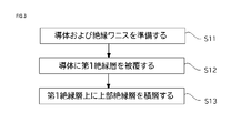
- FIG. 3 is a process diagram in the method for manufacturing an insulated wire according to the present embodiment.
- the present inventors have completed the present disclosure by repeating diligent studies in order to solve the above-mentioned problems. Specifically, attention was paid to suppressing variations in the thickness of the first insulating layer that is in direct contact with the conductor among the insulating layers that cover the linear conductor in the insulated wire. As a result, it has been found that in an insulated wire having a uniform layer thickness of the first insulating layer, the adhesive force between the conductor and the insulating layer is improved as compared with the conventional case, and the present disclosure has been reached.
- the insulated wire according to one aspect of the present disclosure is a linear conductor having a first surface, a second surface facing the first surface, a third surface, and a fourth surface facing the third surface.
- An insulated wire including an insulating layer covering the conductor, the insulating layer comprises a first insulating layer directly in contact with the conductor and one or a plurality of upper insulating layers covering the first insulating layer.
- the first insulating layer has a first coating portion that covers the first surface, a second coating portion that covers the second surface, a third coating portion that covers the third surface, and the fourth surface.
- the layer thickness of the first coating portion is Ta
- the layer thickness of the second coating portion is ta
- the third coating portion is formed.
- the layer thickness of the above is expressed by Tb
- the layer thickness of the fourth coating portion is expressed by tb
- the ratios indicated by Ta / ta and Tb / tb are both 1.6 or less.
- the ratio indicated by the Ta / ta or the Tb / tb may be 1.4 or less in either one. Thereby, the adhesive force between the conductor and the insulating layer can be improved.
- the ratio indicated by the Ta / ta and the Tb / tb may be 1.4 or less. Thereby, the adhesive force between the conductor and the insulating layer can be further improved.
- the cross-sectional shape of the conductor in the cross section may be flat. As a result, the insulated wire can be wound around the core at high density.
- the method for manufacturing an insulated wire is a linear shape having a first surface, a second surface facing the first surface, a third surface, and a fourth surface facing the third surface.
- a method for manufacturing an insulated wire including the conductor and an insulating layer covering the conductor.
- the method for manufacturing the insulated wire includes a step of preparing the conductor and an insulating varnish and the first insulation of the conductor.
- the step of coating the layer and the step of laminating the upper insulating layer on the first insulating layer are included, and the coating step includes a step of applying the insulating varnish to the conductor and a step of applying the insulating varnish to the conductor.
- the step of adjusting the thickness of the insulating varnish and the step of baking the insulating varnish on the conductor are included, and in the step of adjusting the thickness, the distance between the inner wall of the opening of the coating die and the conductor is 0.040 mm. It is carried out by passing the conductor coated with the insulating varnish through the opening as follows.
- the conductor can be coated with the first insulating layer in which the variation in layer thickness is suppressed, so that the insulation with improved adhesion between the conductor and the insulating layer is improved. Electric wires can be manufactured.
- the notation of the form "A to B” means the upper and lower limits of the range (that is, A or more and B or less), and when the unit is not described in A and the unit is described only in B, the unit of A is described.
- the unit and the unit of B are the same.
- FIG. 1 is a perspective view showing a longitudinal direction of the insulated wire according to the present embodiment.
- FIG. 2 is a diagram schematically illustrating a cross section perpendicular to the longitudinal direction of the insulated wire according to the present embodiment.
- the present embodiment is an insulated wire 1 including a linear conductor 11 and an insulating layer 20 covering the conductor 11 as shown in FIGS. 1 and 2.
- the insulating layer 20 has a first insulating layer 21 that is in direct contact with the conductor 11 and one or more upper insulating layers 22 that are arranged on the first insulating layer 21.
- FIGS. 1 and 2 a case where the cross-sectional shape of the conductor 11 in the cross section of the insulated wire 1 is flat is illustrated.
- the first insulating layer covers the two pairs of facing surfaces of the conductor, the first covering portion, the second covering portion, the third covering portion, and the fourth. It has a covering part.
- the first insulating layer covers the two pairs of facing surfaces of the conductor, the first facing surface of the first coating portion and the second coating portion, the third coating portion, and the fourth coating. It has a second facing surface of the part.
- the layer thickness of the first coating portion is Ta
- the layer thickness of the second coating portion is ta
- the layer thickness of the third coating portion is Tb.
- the ratios represented by Ta / ta and Tb / tb are both 1.6 or less.
- the ratio indicated by the Ta / ta or the Tb / tb may be 1.4 or less in either one.
- the ratio indicated by the Ta / ta and the Tb / tb may be 1.4 or less.
- the adhesion between the conductor 11 and the insulating layer 20 can be further improved. The reason why the adhesion between the conductor 11 and the insulating layer 20 is improved in the insulated wire 1 will be described later.
- the insulated wire 1 includes the linear conductor 11 as described above.
- the conductor 11 is a conductor.
- a metal having high conductivity and high mechanical strength is preferable. Specific examples thereof include copper, copper alloys, aluminum, aluminum alloys, nickel, silver, soft iron, steel, and stainless steel.
- the conductor 11 may be a wire formed by forming these metals in a linear shape, or may be a coated wire in which the surface of the wire is coated with another metal, or a stranded wire obtained by twisting a plurality of wires. It may be.
- Examples of the coated wire include, but are not limited to, nickel-coated copper wire, silver-coated copper wire, silver-coated aluminum wire, and copper-coated steel wire.
- the shape of the conductor 11 can be appropriately selected depending on the intended use of the insulated wire 1, the electrical characteristics, and the like.
- the cross-sectional shape of the conductor 11 is flat in order to wind the insulated wire 1 around the core at high density.
- the diameter of the conductor 11 or the length of the outer circumference is not particularly limited, and can be appropriately selected depending on the intended use of the insulated wire 1, the electrical characteristics, and the like.
- the "flat angle" which is one of the cross-sectional shapes of the conductor 11 includes a rectangle and a square, and the four corners of the rectangle and the square are chamfered or have a rounded shape (R shape). Includes shapes that can be squeezed.
- the lower limit of the cross-sectional area of the conductor 11 may be 0.01 mm 2. If the cross-sectional area of the conductor 11 does not satisfy 0.01 mm 2 , the ratio of the volume of the insulating layer 20 to the conductor 11 becomes large, and the volumetric efficiency of the coil formed by using the insulated wire 1 may decrease.
- the upper limit of the cross-sectional area of the conductor 11 may be 20 mm 2. When the cross-sectional area of the conductor 11 exceeds 20 mm 2 , it becomes necessary to increase the thickness of the insulating layer 20 in order to sufficiently improve the insulating property of the insulated wire 1, and as a result, the diameter of the insulated wire 1 becomes large and the core becomes tall. It tends to be difficult to wind with density.
- the lower limit of the cross-sectional area of the conductor 11 may be 0.1 mm 2. If the cross-sectional area of the conductor 11 does not satisfy 0.1 mm 2 , the conductor resistance when energized increases, which may cause heat generation loss.
- the upper limit of the cross-sectional area of the conductor 11 may be 10 mm 2. If the cross-sectional area of the conductor 11 exceeds 10 mm 2 , it may be difficult to bend the coil formed by using the insulated wire 1.
- the insulated wire 1 includes an insulating layer 20 that covers the conductor 11 as described above.
- the insulating layer 20 has a first insulating layer 21 that is in direct contact with the conductor 11 and one or more upper insulating layers 22 that are arranged on the first insulating layer 21.
- Examples of the resin constituting the insulating layer 20 include thermosetting resins such as polyvinyl formal resin, polyurethane resin, alkyl resin, epoxy resin, phenoxy resin, polyester resin, polyesterimide resin, polyesteramideimide resin, polyamideimide resin, and polyimide resin. , And thermoplastic resins such as polyetherimide resin, polyether ether ketone resin, polyether sulfone resin, and polyimide resin. These resins are used alone or in admixture of two or more. It may be a thermosetting polyimide resin. The strength and heat resistance of the insulating layer 20 can be improved.
- thermosetting resins such as polyvinyl formal resin, polyurethane resin, alkyl resin, epoxy resin, phenoxy resin, polyester resin, polyesterimide resin, polyesteramideimide resin, polyamideimide resin, and polyimide resin.
- thermoplastic resins such as polyetherimide resin, polyether ether ketone resin, polyether sulfone resin, and polyimide resin.
- the first insulating layer 21 and the upper insulating layer 22 constituting the insulating layer 20 may be formed by selecting the same type of resin from the various resins described above, and different types of resins may be used. Both may be formed by selection.
- the lower limit of the thickness of the insulating layer 20 (the total thickness of the first insulating layer 21 and the upper insulating layer 22) may be 5 ⁇ m. If the thickness of the insulating layer 20 is less than 5 ⁇ m, the insulating layer 20 tends to be torn, and the insulation of the conductor 11 may be insufficient.
- the upper limit of the thickness of the insulating layer 20 may be 200 ⁇ m. If the thickness of the insulating layer 20 exceeds 200 ⁇ m, the volumetric efficiency of the coil or the like formed by using the insulated wire 1 tends to decrease.
- the thickness of the insulating layer 20 means the average value of the thicknesses of the insulating layers 20 covering the two pairs of facing surfaces (upper surface, lower surface, left surface, right surface) of the conductor 11. Specifically, the surface to be measured is produced by polishing the cross section that appears by cutting the insulated wire 1 on a surface that is perpendicular to the longitudinal direction thereof. Next, an image is obtained by imaging the measurement target surface with a digital microscope VHX-7000 (manufactured by KEYENCE CORPORATION).
- the thickness of the insulating layer 20 covering the two pairs of facing surfaces of the conductor 11 in the image for example, one location each is selected from the upper surface, the lower surface, the left surface, and the right surface of the conductor 11, and a total of four locations are selected.
- An average value can be calculated from the value obtained by measuring the thickness of the insulating layer 20 in the above, and this can be used as the thickness of the insulating layer 20.
- the first insulating layer 21 is an insulating layer that is in direct contact with the conductor 11.
- the first insulating layer 21 means an insulating layer formed by baking based on an insulating varnish applied so as to be in direct contact with the conductor 11 as described later.
- the first insulating layer 21 has a first coating portion, a second coating portion, a third coating portion, and a fourth coating portion as portions covering the two pairs of facing surfaces of the conductor 11.
- the first insulating layer covers the two pairs of facing surfaces of the conductor, the first facing surface of the first coating portion and the second coating portion, the third coating portion, and the fourth coating. It has a second facing surface of the part.
- the layer thickness of the first coating portion of the first insulation layer 21 is Ta
- the layer thickness of the second coating portion is ta
- the layer of the third coating portion is the layer.
- the ratios represented by Ta / ta and Tb / tb are both 1.6 or less.
- Ta represents the layer thickness of the first insulating layer 21 covering the lower surface of the conductor 11
- ta represents the layer thickness of the first insulating layer 21 covering the upper surface of the conductor 11.
- Tb represents the layer thickness of the first insulating layer 21 covering the left surface of the conductor 11, and tb represents the layer thickness of the first insulating layer 21 covering the right surface of the conductor 11.
- Ta is assumed to be larger than ta or the same value (layer thickness) (Ta ⁇ ta), and Tb is assumed to be larger than tb or the same value (layer thickness).
- Tb is assumed to be larger than tb or the same value (layer thickness).
- the ratios represented by Ta / ta and Tb / tb are both 1.6 or less.
- the ratio represented by the Ta / ta and the Tb / tb may be 1.4 or less, or 1.1 or less.
- the ratio represented by the Ta / ta and the Tb / tb is 1.0. In these cases, the adhesion between the conductor and the insulating layer can be further improved.
- the first insulating layer 21, in which the ratios indicated by both Ta / ta and Tb / tb are 1.6 or less, is formed by using, for example, a conductor 11 coated with an insulating varnish as described later on the inner wall of the opening of the coating die. It can be obtained by passing the conductor through the opening of the coating die so that the distance between the conductor and the conductor is 0.040 mm or less.
- the ratio represented by the Ta / ta and the Tb / tb of the first insulating layer 21 of the insulated wire 1 is 1.6 or less, it is insulated from the conductor 11 as compared with the conventional insulated wire. It is even more excellent in the adhesion with the layer 20. The reason is not clear in detail, but it is thought to be as follows.
- a portion thicker than the layer thickness of the first facing surface and the layer thickness of the second facing surface (hereinafter, also referred to as "thickened portion"). ) May exist.
- the adhesion between the thickened portion and the conductor tends to decrease. This is because it is presumed that the thickened portion may not be sufficiently baked due to insufficient heat input during baking of the insulating varnish or difficulty in volatilizing and dissipating the solvent of the insulating varnish. .. Therefore, in order to obtain sufficient adhesion between the conductor and the insulating layer, it is presumed that it is important that the thickened portion is absent in the first insulating layer 21 that is in direct contact with the conductor 11.
- the variation in the layer thickness of the first insulating layer 21 is suppressed so that the above-mentioned thickened portion does not exist, and the ratios shown by the Ta / ta and the Tb / tb are both 1.6 or less. In this case, it is considered that an excellent adhesive force can be provided between the conductor 11 and the insulating layer 20.
- the layer thickness (Ta, ta, Tb, tb) of the first insulating layer can be measured by the same method as the method for measuring the thickness of the insulating layer 20 described above. First, an image is obtained in the same manner as the method for measuring the thickness of the insulating layer 20. Next, one location is selected from each of the upper surface, the lower surface, the left surface, and the right surface of the conductor 11 in the image, and the layer thickness of the first insulating layer 21 at these four locations in total, in other words, the first coating portion and the second coating portion. It can be obtained by measuring the layer thicknesses Ta, ta, Tb and tb of the third coating portion and the fourth coating portion.
- the upper insulating layer 22 is one or a plurality of insulating layers arranged on the first insulating layer 21.
- the upper insulating layer 22 can be laminated on the first insulating layer 21 by a conventionally known method as described later.
- the specific number of layers of the upper insulating layer 22 arranged on the first insulating layer 21 can be appropriately selected depending on the intended use of the insulated wire 1, the electrical characteristics, and the like, but usually, the upper insulating layer 22 is the first. 1 to 100 layers can be arranged on the insulating layer 21.
- the thickness of the upper insulating layer 22 can be obtained as the difference between the thickness of the insulating layer 20 and the thickness of the first insulating layer 21 obtained by the measurement method described above.
- the interface between the upper insulating layer 22 and the first insulating layer 21 is clear in the cross section perpendicular to the longitudinal direction of the insulated wire 1. Can be specified in. Further, when the upper insulating layer 22 is a plurality of layers, the interface between the plurality of layers can be clearly specified.
- the adhesion between the conductor 11 and the insulating layer 20 can be evaluated by the following method. First, the insulated wire 1 is obtained by the manufacturing method described later. Next, two opposed cuts are made in the insulating layer 20 of the insulated wire 1 in parallel with the longitudinal direction of the insulated wire 1 so as to reach the conductor 11 using a utility knife. Here, the distance between the two notches is 1.0 mm.
- the peel strength is obtained by pulling the peelable portion under the condition of a tensile speed of 100 mm / min.
- the peel strength (unit: N / mm) obtained thereby can be evaluated as the adhesion between the conductor 11 and the insulating layer 20. As a result, it can be evaluated that the larger the value of the peel strength, the better the adhesion between the conductor 11 and the insulating layer 20.
- the insulated wire 1 according to the present embodiment can be obtained by using the following method for manufacturing an insulated wire, for example, from the viewpoint of manufacturing with good yield. That is, the method for manufacturing the insulated wire 1 according to the present embodiment includes a linear conductor 11 and an insulating layer 20 that covers the conductor 11, and the insulating layer 20 includes a first insulating layer 21 that is in direct contact with the conductor 11. This is a method for manufacturing an insulated wire 1 having one or a plurality of upper insulating layers 22 arranged on the first insulating layer 21.
- the method for manufacturing the insulated wire 1 includes a step of preparing the conductor 11 and an insulating varnish (first step), a step of coating the conductor 11 with the first insulating layer 21 (second step), and a first insulating layer 21. It includes a step (third step) of laminating the upper insulating layer 22 on the top.
- the coating step (second step) includes a step of applying an insulating varnish to the conductor 11 (step A), a step of adjusting the thickness of the insulating varnish applied to the conductor 11 (step B), and the insulating varnish. Is included in the conductor 11 (step C). In the step of adjusting the thickness (step B), the conductor 11 coated with the insulating varnish is passed through the opening so that the distance between the inner wall of the opening of the coating die and the conductor 11 is 0.040 mm or less. Is executed by.
- the conductor 11 can be covered with the first insulating layer 21 in which the variation in layer thickness is suppressed, so that the adhesion between the conductor 11 and the insulating layer 20 can be applied. It is possible to manufacture the insulated electric wire 1 in which the above is improved.
- each step included in the method for manufacturing the insulated wire 1 according to the present embodiment will be described in detail.
- the first step is a step of preparing the conductor 11 and the insulating varnish (S11).
- the conductor 11 can be prepared, for example, by obtaining a commercially available product. It can also be prepared by casting, stretching, linearly drawing, and further softening the above-mentioned metal as the material of the conductor 11.
- the insulating varnish can be prepared by diluting the above-mentioned resin as the material of the insulating layer 20 or a resin precursor thereof with a solvent.
- the resin solid content concentration in the insulating varnish can be the conventional concentration known for the purpose of producing this type of insulated wire.
- the lower limit of the resin solid content concentration in the insulating varnish may be 15% by mass.
- the resin solid content concentration does not satisfy 15% by mass, the film thickness of each layer after baking becomes thin, and the productivity may decrease.
- the upper limit of the resin solid content concentration in the insulating varnish may be 50% by mass. If the resin solid content concentration exceeds 50% by mass, the applied insulating varnish becomes thick and the film may foam during baking.
- the resin solid content concentration means the concentration of the resin precursor.
- the insulating varnish may contain a curing agent in addition to the above-mentioned solvent, resin or resin precursor thereof, and may further contain a filler, various additives and the like.
- a known organic solvent can be used. Specifically, polar organic solvents such as N-methyl-2-pyrrolidone, N, N-dimethylacetamide, N, N-dimethylformamide, dimethylsulfoxide, tetramethylurea, hexaethylphosphate triamide, and ⁇ -butyrolactone; acetone.
- polar organic solvents such as N-methyl-2-pyrrolidone, N, N-dimethylacetamide, N, N-dimethylformamide, dimethylsulfoxide, tetramethylurea, hexaethylphosphate triamide, and ⁇ -butyrolactone; acetone.
- the curing agent one having a function of curing the resin in step B described later or a function of promoting the polymerization of the resin precursor can be used.
- alicyclic acid anhydrides such as methyltetrahydrophthalic anhydride, aliphatic acid anhydrides, aromatic acid anhydrides imidazole, triethylamine, titanium compounds, isocyanate compounds, blocked isocyanates, urea, melamine compounds and Examples include acetylene derivatives.
- These curing agents are appropriately selected depending on the type of resin or resin precursor in the insulating varnish.
- titanium-based compound examples include tetrapropyl titanate, tetraisopropyl titanate, tetramethyl titanate, tetrabutyl titanate, and tetrahexyl titanate.
- isocyanate-based compound examples include aromatic diisocyanates such as tolylene diisocyanate (TDI), diphenylmethane diisocyanate (MDI), p-phenylenedi isocyanate, and naphthalene diisocyanate; hexamethylene diisocyanate (HDI), 2,2,4-trimethylhexanediisocyanate, and the like.
- Aromatic diisocyanates having 3 to 12 carbon atoms such as lysine diisocyanate; 1,4-cyclohexanediisocyanate (CDI), isophorone diisocyanate (IPDI), 4,4'-dicyclohexylmethane diisocyanate (hydrogenated MDI), methylcyclohexanediisocyanate, isopropylidene Dicyclohexyl-4,4'-diisocyanate, 1,3-diisocyanatomethylcyclohexane (hydrogenated XDI), hydrogenated TDI, 2,5-bis (isocyanatomethyl) -bicyclo [2,2,1] heptane, 2 , 6-Bis (isocyanatomethyl) -bicyclo [2,2,1] heptane and other alicyclic isocyanates with 5 to 18 carbon atoms; aromatics such as xylylene diisocyanate (XDI)
- blocked isocyanate examples include diphenylmethane-4,4′-diisocyanate (MDI), diphenylmethane-3,3′-diisocyanate, diphenylmethane-3,4′-diisocyanate, diphenylether-4,4′-diisocyanate, and benzophenone-4,4.
- MDI diphenylmethane-4,4′-diisocyanate
- diphenylmethane-3,3′-diisocyanate diphenylmethane-3,4′-diisocyanate
- diphenylether-4,4′-diisocyanate diphenylether-4,4′-diisocyanate
- benzophenone-4,4 examples include benzophenone-4,4.
- melamine compound examples include methylated melamine, butylated melamine, methylolated melamine, butyrolylated melamine and the like.
- acetylene derivative examples include ethynylaniline and ethynylphthalic anhydride.
- the second step is a step of coating the conductor 11 with the first insulating layer 21 (S12).
- the second step is a step of applying an insulating varnish to the conductor 11 (step A), a step of adjusting the thickness of the insulating varnish applied to the conductor 11 (step B), and baking the insulating varnish on the conductor 11.
- step (C step) includes step (C step).
- Step A The step A is a step of applying the insulating varnish prepared in the first step to the conductor 11.
- Step B The B step is a step of adjusting the thickness of the insulating varnish applied to the conductor 11. Further, the step B is executed by passing the conductor 11 coated with the insulating varnish through the opening so that the distance between the inner wall of the opening of the coating die and the conductor 11 is 0.040 mm or less. That is, in step B, the thickness of the insulating varnish coated on the conductor 11 is adjusted by using a coating die having an opening.
- the C step is a step of baking the insulating varnish on the conductor 11.
- step C the first insulating layer 21 that is in direct contact with the conductor 11 is formed by the baking process. Specifically, the conductor 11 coated with the insulating varnish is placed in the baking furnace through the steps A and B, and the insulating varnish is baked onto the conductor 11. As a result, the solvent in the insulating varnish is gasified and the resin is solidified, so that the first insulating layer 21 in direct contact with the conductor 11 can be formed.
- the layer thickness of the first insulating layer 21 formed in direct contact with the conductor 11 is also uniform, and thus the layer is formed. It is possible to suppress the variation in thickness.
- the baking temperature and time of the insulating varnish in the baking furnace are appropriately selected from the temperature and time conditions known for the production of this type of insulated wire according to the type of resin in the insulating varnish. be able to.
- the third step is a step of laminating the upper insulating layer 22 on the first insulating layer 21 (S13).
- one or a plurality of upper insulating layers 22 are laminated on the first insulating layer 21 by repeating the application of the insulating varnish and the baking of the insulating varnish until the insulating layer 20 has a predetermined thickness. ..
- As a method for applying and baking the insulating varnish conventionally known methods can be used. Further, by applying the insulating varnish and baking the insulating varnish according to the above-mentioned steps A and B, it is possible to laminate the upper insulating layer 22 on the first insulating layer 21 in the required number of layers. ..
- the insulating layer obtained by applying the insulating varnish once and baking the insulating varnish is referred to as a "one layer” insulating layer, and the insulating varnish is applied a plurality of times and the insulating varnish is applied.
- the insulating layer obtained by baking the above material is referred to as a "multi-layer” insulating layer.
- the insulating layer obtained by applying the insulating varnish once and baking it once is referred to as a "one layer” insulating layer.
- An insulating layer obtained by applying an insulating varnish once and baking it once is called a "plurality" insulating layer.
- the linear conductor 11 and the insulating layer 20 that covers the conductor 11 are included, and the insulating layer 20 is arranged on the first insulating layer 21 that is in direct contact with the conductor 11 and the first insulating layer 21.
- an insulated wire 1 having a plurality of upper insulating layers 22 can be manufactured. In the insulated wire 1 manufactured by the above-mentioned manufacturing method, the variation in the layer thickness of the first insulating layer 21 is suppressed.
- the first insulating layer 21 has a first coating portion, a second coating portion, a third coating portion, and a fourth coating portion as portions covering the two pairs of facing surfaces of the conductor 11.
- the first insulating layer 21 covers the two pairs of facing surfaces of the conductor, and is the first facing surface, the third covering portion, and the fourth covering portion of the first covering portion and the second covering portion. It has a second facing surface of the covering.
- the layer thickness of the first coating portion is Ta
- the layer thickness of the second coating portion is ta
- the layer thickness of the third coating portion is Tb
- the fourth coating portion In the cross section perpendicular to the longitudinal direction of the insulated wire 1, the layer thickness of the first coating portion is Ta, the layer thickness of the second coating portion is ta, the layer thickness of the third coating portion is Tb, and the fourth coating portion.
- the ratios represented by Ta / ta and Tb / tb are both 1.6 or less.
- the adhesion between the conductor and the insulating layer was determined according to the method for measuring the adhesion between the conductor and the insulating layer described above. Next, the adhesion was evaluated based on the following criteria.
- the variation ratio of the thickness of the insulating layer of each sample obtained based on the above formula was evaluated based on the following criteria. If the variation ratio exceeds 20%, it is considered that the uniformity of the layer thickness of the insulating layer is low and the adhesion between the conductor and the insulating layer is insufficient. OK: The variation ratio of the insulating layer is 20% or less. NG: The variation ratio of the insulating layer exceeds 20%.
- an insulating varnish was prepared by diluting a polyamic acid (polyamide precursor) having a weight average molecular weight of 37500 with N-methyl-2-pyrrolidone (solvent).
- a polyamic acid polyamide precursor
- solvent N-methyl-2-pyrrolidone
- the shape of the cross section that appears when copper is cast, stretched, drawn, and softened to cut it on a plane perpendicular to the longitudinal direction is a flat shape as shown in FIG. 2 (cross-sectional area: 5 mm 2 ).
- a linear conductor 11 having the above was produced.
- step A Next, by immersing the conductor 11 in the insulating varnish, the insulating varnish is applied to the conductor 11 (step A), and the above-mentioned insulating varnish is formed in the opening of the coating die having a shape similar to the cross-sectional shape of the conductor 11.
- step B Was passed through the conductor 11 coated with (step B). At this time, the maximum distance between the conductor 11 and the inner wall of the opening of the coating die was 0.027 mm.
- step C The baking temperature of the insulating varnish in the baking furnace was 450 ° C., and the baking time was 30 seconds.
- the first insulating layer 21 that is in direct contact with the conductor 11 is formed.
- the upper insulating layer 22 was laminated on the first insulating layer 21 by repeating the application of the insulating varnish and the baking of the insulating varnish on the first insulating layer 21. Specifically, the insulating varnish is applied onto the first insulating layer 21, and the insulating varnish is further passed through an opening of a coating die having a shape similar to the cross-sectional shape of the conductor 11 to provide upper insulation on the first insulating layer 21. The first layer of layer 22 was formed. Next, the insulating varnish is applied onto the first layer of the upper insulating layer 22, and the baking treatment described above is further performed to form the second layer of the upper insulating layer 22, and a plurality of such operations are performed. Repeated times. As described above, the insulating layer 20 having a total of 25 layers of the first insulating layer 21 and the upper insulating layer 22 was formed on the conductor 11 to obtain the insulated wire 1.
- Example 2 to Sample 4 Insulated wire by the same method as sample 1 except that the maximum distance between the conductor and the inner wall of the opening of the coating die when the conductor is passed through the opening of the coating die is as shown in Table 1. Manufactured.
- Samples 1 to 3 had a ratio of Ta / ta and Tb / tb of 1.6 or less. In that case, Samples 1 to 3 were superior in adhesion between the conductor and the insulating layer as compared with Sample 4, in which any of the ratios represented by Ta / ta and Tb / tb exceeded 1.6. All of the samples 1 to 4 showed an OK evaluation (20% or less) in terms of the variation ratio of the thickness of the insulating layer.
Landscapes
- Engineering & Computer Science (AREA)
- Manufacturing & Machinery (AREA)
- Power Engineering (AREA)
- Processes Specially Adapted For Manufacturing Cables (AREA)
- Insulated Conductors (AREA)
Priority Applications (2)
| Application Number | Priority Date | Filing Date | Title |
|---|---|---|---|
| CN202180027223.5A CN115398565A (zh) | 2020-04-15 | 2021-03-18 | 绝缘电线及其制造方法 |
| JP2022515260A JP7685481B2 (ja) | 2020-04-15 | 2021-03-18 | 絶縁電線およびその製造方法 |
Applications Claiming Priority (2)
| Application Number | Priority Date | Filing Date | Title |
|---|---|---|---|
| JP2020-073067 | 2020-04-15 | ||
| JP2020073067 | 2020-04-15 |
Publications (1)
| Publication Number | Publication Date |
|---|---|
| WO2021210336A1 true WO2021210336A1 (ja) | 2021-10-21 |
Family
ID=78083829
Family Applications (1)
| Application Number | Title | Priority Date | Filing Date |
|---|---|---|---|
| PCT/JP2021/010963 Ceased WO2021210336A1 (ja) | 2020-04-15 | 2021-03-18 | 絶縁電線およびその製造方法 |
Country Status (3)
| Country | Link |
|---|---|
| JP (1) | JP7685481B2 (https=) |
| CN (1) | CN115398565A (https=) |
| WO (1) | WO2021210336A1 (https=) |
Cited By (2)
| Publication number | Priority date | Publication date | Assignee | Title |
|---|---|---|---|---|
| JPWO2023026591A1 (https=) * | 2021-08-24 | 2023-03-02 | ||
| EP4310865A1 (en) * | 2022-07-22 | 2024-01-24 | Proterial, Ltd. | Insulated wire and method for manufacturing insulated wire |
Citations (1)
| Publication number | Priority date | Publication date | Assignee | Title |
|---|---|---|---|---|
| JP2012048919A (ja) * | 2010-08-25 | 2012-03-08 | Sumitomo Electric Wintec Inc | 塗布ダイスおよび絶縁電線の製造方法 |
Family Cites Families (1)
| Publication number | Priority date | Publication date | Assignee | Title |
|---|---|---|---|---|
| JPS60202613A (ja) * | 1984-03-27 | 1985-10-14 | 昭和電線電纜株式会社 | 静電粉体塗装法による絶縁電線の製造方法 |
-
2021
- 2021-03-18 CN CN202180027223.5A patent/CN115398565A/zh active Pending
- 2021-03-18 JP JP2022515260A patent/JP7685481B2/ja active Active
- 2021-03-18 WO PCT/JP2021/010963 patent/WO2021210336A1/ja not_active Ceased
Patent Citations (1)
| Publication number | Priority date | Publication date | Assignee | Title |
|---|---|---|---|---|
| JP2012048919A (ja) * | 2010-08-25 | 2012-03-08 | Sumitomo Electric Wintec Inc | 塗布ダイスおよび絶縁電線の製造方法 |
Cited By (5)
| Publication number | Priority date | Publication date | Assignee | Title |
|---|---|---|---|---|
| JPWO2023026591A1 (https=) * | 2021-08-24 | 2023-03-02 | ||
| JP7811917B2 (ja) | 2021-08-24 | 2026-02-06 | 住友電気工業株式会社 | 絶縁電線 |
| EP4310865A1 (en) * | 2022-07-22 | 2024-01-24 | Proterial, Ltd. | Insulated wire and method for manufacturing insulated wire |
| US20240029923A1 (en) * | 2022-07-22 | 2024-01-25 | Proterial, Ltd. | Insulated wire and method for manufacturing insulated wire |
| US12476026B2 (en) * | 2022-07-22 | 2025-11-18 | Proterial, Ltd. | Insulated wire and method for manufacturing insulated wire |
Also Published As
| Publication number | Publication date |
|---|---|
| JPWO2021210336A1 (https=) | 2021-10-21 |
| JP7685481B2 (ja) | 2025-05-29 |
| CN115398565A (zh) | 2022-11-25 |
Similar Documents
| Publication | Publication Date | Title |
|---|---|---|
| JP6306220B2 (ja) | 絶縁電線及び絶縁層形成用ワニス | |
| JP5626530B2 (ja) | 絶縁塗料及びその製造方法並びにそれを用いた絶縁電線及びその製造方法 | |
| US10991477B2 (en) | Insulated electrical cable | |
| JP7685481B2 (ja) | 絶縁電線およびその製造方法 | |
| JP2018029004A (ja) | 自己潤滑性絶縁電線 | |
| JPWO2018174113A1 (ja) | 絶縁電線 | |
| CN104246914B (zh) | 绝缘电线及其制造方法 | |
| US10468153B2 (en) | Insulated electric wire and method for producing insulated electric wire | |
| US20240052199A1 (en) | Insulated electrical wire and production method therefor | |
| JP7214625B2 (ja) | 絶縁電線 | |
| JP2016046061A (ja) | 絶縁電線及び絶縁電線の製造方法 | |
| WO2017138284A1 (ja) | 絶縁電線 | |
| JP7811917B2 (ja) | 絶縁電線 | |
| JP2001155551A (ja) | 絶縁電線 | |
| JP5342277B2 (ja) | 多層絶縁電線 | |
| JP4782906B2 (ja) | 絶縁電線 | |
| CN120226097A (zh) | 绝缘电线以及树脂组合物 | |
| JP2017045662A (ja) | 絶縁電線及び絶縁層形成用ワニス | |
| CN116829659B (zh) | 绝缘层形成用树脂清漆 | |
| WO2022190657A1 (ja) | 絶縁電線 | |
| JP2012051966A (ja) | エポキシ変性ポリフェニレンエーテル及びそれを用いた絶縁電線、電機コイル、モータ | |
| WO2023153063A1 (ja) | 絶縁電線及び絶縁電線の製造方法 | |
| JP6690986B2 (ja) | 絶縁電線及び絶縁電線の製造方法 | |
| JPH0752998B2 (ja) | 超耐熱ボイスコイルの製造法 |
Legal Events
| Date | Code | Title | Description |
|---|---|---|---|
| 121 | Ep: the epo has been informed by wipo that ep was designated in this application |
Ref document number: 21788084 Country of ref document: EP Kind code of ref document: A1 |
|
| ENP | Entry into the national phase |
Ref document number: 2022515260 Country of ref document: JP Kind code of ref document: A |
|
| NENP | Non-entry into the national phase |
Ref country code: DE |
|
| 122 | Ep: pct application non-entry in european phase |
Ref document number: 21788084 Country of ref document: EP Kind code of ref document: A1 |