WO2021210336A1 - Insulated wire and method for manufacturing same - Google Patents
Insulated wire and method for manufacturing same Download PDFInfo
- Publication number
- WO2021210336A1 WO2021210336A1 PCT/JP2021/010963 JP2021010963W WO2021210336A1 WO 2021210336 A1 WO2021210336 A1 WO 2021210336A1 JP 2021010963 W JP2021010963 W JP 2021010963W WO 2021210336 A1 WO2021210336 A1 WO 2021210336A1
- Authority
- WO
- WIPO (PCT)
- Prior art keywords
- conductor
- insulating layer
- insulated wire
- insulating
- layer
- Prior art date
Links
Images


Classifications
-
- H—ELECTRICITY
- H01—ELECTRIC ELEMENTS
- H01B—CABLES; CONDUCTORS; INSULATORS; SELECTION OF MATERIALS FOR THEIR CONDUCTIVE, INSULATING OR DIELECTRIC PROPERTIES
- H01B13/00—Apparatus or processes specially adapted for manufacturing conductors or cables
-
- H—ELECTRICITY
- H01—ELECTRIC ELEMENTS
- H01B—CABLES; CONDUCTORS; INSULATORS; SELECTION OF MATERIALS FOR THEIR CONDUCTIVE, INSULATING OR DIELECTRIC PROPERTIES
- H01B13/00—Apparatus or processes specially adapted for manufacturing conductors or cables
- H01B13/06—Insulating conductors or cables
- H01B13/16—Insulating conductors or cables by passing through or dipping in a liquid bath; by spraying
-
- H—ELECTRICITY
- H01—ELECTRIC ELEMENTS
- H01B—CABLES; CONDUCTORS; INSULATORS; SELECTION OF MATERIALS FOR THEIR CONDUCTIVE, INSULATING OR DIELECTRIC PROPERTIES
- H01B7/00—Insulated conductors or cables characterised by their form
- H01B7/02—Disposition of insulation
-
- H—ELECTRICITY
- H01—ELECTRIC ELEMENTS
- H01F—MAGNETS; INDUCTANCES; TRANSFORMERS; SELECTION OF MATERIALS FOR THEIR MAGNETIC PROPERTIES
- H01F5/00—Coils
- H01F5/06—Insulation of windings
Definitions
- This disclosure relates to an insulated wire and a method for manufacturing an insulated wire.
- This application claims priority based on Japanese Application No. 2020-073067 filed on April 15, 2020, and incorporates all the contents described in the Japanese application.
- An insulated wire having a linear conductor and an insulating layer covering the conductor is known.
- the insulated wire is suitably used as a coil for, for example, a motor or a transformer.
- International Publication No. 2013/0733397 discloses that the adhesive force between the conductor and the insulating layer is improved by suppressing the variation in the thickness of the insulating layer in the insulated wire.
- the insulated wire of the present disclosure includes a linear conductor having a first surface, a second surface facing the first surface, a third surface, and a fourth surface facing the third surface, and insulation covering the conductor.
- An insulated wire including a layer, wherein the insulating layer has a first insulating layer that is in direct contact with the conductor and one or a plurality of upper insulating layers that cover the first insulating layer, and the first insulating layer.
- the layer includes a first coating portion that covers the first surface, a second coating portion that covers the second surface, a third coating portion that covers the third surface, and a fourth coating portion that covers the fourth surface.
- the layer thickness of the first coating portion is Ta
- the layer thickness of the second coating portion is ta
- the layer thickness of the third coating portion is Tb
- the layer thickness of the fourth coating portion is represented by tb
- the ratios represented by Ta / ta and Tb / tb are both 1.6 or less.
- a linear conductor having a first surface, a second surface facing the first surface, a third surface, and a fourth surface facing the third surface, and the conductor are used.
- a method for manufacturing an insulated wire including an insulating layer to be coated wherein the method for manufacturing the insulated wire includes a step of preparing the conductor and an insulating varnish, and a step of coating the conductor with the first insulating layer.
- the step of laminating the upper insulating layer on the first insulating layer includes the step of applying the insulating varnish to the conductor and the step of applying the insulating varnish to the conductor to adjust the thickness of the insulating varnish applied to the conductor.
- the step of adjusting the thickness includes the step of baking the insulating varnish on the conductor, and the step of adjusting the thickness is such that the distance between the inner wall of the opening of the coating die and the conductor is 0.040 mm or less. This is carried out by passing the conductor coated with an insulating varnish through the opening.
- FIG. 1 is a perspective view showing a longitudinal direction of the insulated wire according to the present embodiment.
- FIG. 2 is a diagram schematically illustrating a cross section perpendicular to the longitudinal direction of the insulated wire according to the present embodiment.
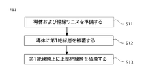
- FIG. 3 is a process diagram in the method for manufacturing an insulated wire according to the present embodiment.
- the present inventors have completed the present disclosure by repeating diligent studies in order to solve the above-mentioned problems. Specifically, attention was paid to suppressing variations in the thickness of the first insulating layer that is in direct contact with the conductor among the insulating layers that cover the linear conductor in the insulated wire. As a result, it has been found that in an insulated wire having a uniform layer thickness of the first insulating layer, the adhesive force between the conductor and the insulating layer is improved as compared with the conventional case, and the present disclosure has been reached.
- the insulated wire according to one aspect of the present disclosure is a linear conductor having a first surface, a second surface facing the first surface, a third surface, and a fourth surface facing the third surface.
- An insulated wire including an insulating layer covering the conductor, the insulating layer comprises a first insulating layer directly in contact with the conductor and one or a plurality of upper insulating layers covering the first insulating layer.
- the first insulating layer has a first coating portion that covers the first surface, a second coating portion that covers the second surface, a third coating portion that covers the third surface, and the fourth surface.
- the layer thickness of the first coating portion is Ta
- the layer thickness of the second coating portion is ta
- the third coating portion is formed.
- the layer thickness of the above is expressed by Tb
- the layer thickness of the fourth coating portion is expressed by tb
- the ratios indicated by Ta / ta and Tb / tb are both 1.6 or less.
- the ratio indicated by the Ta / ta or the Tb / tb may be 1.4 or less in either one. Thereby, the adhesive force between the conductor and the insulating layer can be improved.
- the ratio indicated by the Ta / ta and the Tb / tb may be 1.4 or less. Thereby, the adhesive force between the conductor and the insulating layer can be further improved.
- the cross-sectional shape of the conductor in the cross section may be flat. As a result, the insulated wire can be wound around the core at high density.
- the method for manufacturing an insulated wire is a linear shape having a first surface, a second surface facing the first surface, a third surface, and a fourth surface facing the third surface.
- a method for manufacturing an insulated wire including the conductor and an insulating layer covering the conductor.
- the method for manufacturing the insulated wire includes a step of preparing the conductor and an insulating varnish and the first insulation of the conductor.
- the step of coating the layer and the step of laminating the upper insulating layer on the first insulating layer are included, and the coating step includes a step of applying the insulating varnish to the conductor and a step of applying the insulating varnish to the conductor.
- the step of adjusting the thickness of the insulating varnish and the step of baking the insulating varnish on the conductor are included, and in the step of adjusting the thickness, the distance between the inner wall of the opening of the coating die and the conductor is 0.040 mm. It is carried out by passing the conductor coated with the insulating varnish through the opening as follows.
- the conductor can be coated with the first insulating layer in which the variation in layer thickness is suppressed, so that the insulation with improved adhesion between the conductor and the insulating layer is improved. Electric wires can be manufactured.
- the notation of the form "A to B” means the upper and lower limits of the range (that is, A or more and B or less), and when the unit is not described in A and the unit is described only in B, the unit of A is described.
- the unit and the unit of B are the same.
- FIG. 1 is a perspective view showing a longitudinal direction of the insulated wire according to the present embodiment.
- FIG. 2 is a diagram schematically illustrating a cross section perpendicular to the longitudinal direction of the insulated wire according to the present embodiment.
- the present embodiment is an insulated wire 1 including a linear conductor 11 and an insulating layer 20 covering the conductor 11 as shown in FIGS. 1 and 2.
- the insulating layer 20 has a first insulating layer 21 that is in direct contact with the conductor 11 and one or more upper insulating layers 22 that are arranged on the first insulating layer 21.
- FIGS. 1 and 2 a case where the cross-sectional shape of the conductor 11 in the cross section of the insulated wire 1 is flat is illustrated.
- the first insulating layer covers the two pairs of facing surfaces of the conductor, the first covering portion, the second covering portion, the third covering portion, and the fourth. It has a covering part.
- the first insulating layer covers the two pairs of facing surfaces of the conductor, the first facing surface of the first coating portion and the second coating portion, the third coating portion, and the fourth coating. It has a second facing surface of the part.
- the layer thickness of the first coating portion is Ta
- the layer thickness of the second coating portion is ta
- the layer thickness of the third coating portion is Tb.
- the ratios represented by Ta / ta and Tb / tb are both 1.6 or less.
- the ratio indicated by the Ta / ta or the Tb / tb may be 1.4 or less in either one.
- the ratio indicated by the Ta / ta and the Tb / tb may be 1.4 or less.
- the adhesion between the conductor 11 and the insulating layer 20 can be further improved. The reason why the adhesion between the conductor 11 and the insulating layer 20 is improved in the insulated wire 1 will be described later.
- the insulated wire 1 includes the linear conductor 11 as described above.
- the conductor 11 is a conductor.
- a metal having high conductivity and high mechanical strength is preferable. Specific examples thereof include copper, copper alloys, aluminum, aluminum alloys, nickel, silver, soft iron, steel, and stainless steel.
- the conductor 11 may be a wire formed by forming these metals in a linear shape, or may be a coated wire in which the surface of the wire is coated with another metal, or a stranded wire obtained by twisting a plurality of wires. It may be.
- Examples of the coated wire include, but are not limited to, nickel-coated copper wire, silver-coated copper wire, silver-coated aluminum wire, and copper-coated steel wire.
- the shape of the conductor 11 can be appropriately selected depending on the intended use of the insulated wire 1, the electrical characteristics, and the like.
- the cross-sectional shape of the conductor 11 is flat in order to wind the insulated wire 1 around the core at high density.
- the diameter of the conductor 11 or the length of the outer circumference is not particularly limited, and can be appropriately selected depending on the intended use of the insulated wire 1, the electrical characteristics, and the like.
- the "flat angle" which is one of the cross-sectional shapes of the conductor 11 includes a rectangle and a square, and the four corners of the rectangle and the square are chamfered or have a rounded shape (R shape). Includes shapes that can be squeezed.
- the lower limit of the cross-sectional area of the conductor 11 may be 0.01 mm 2. If the cross-sectional area of the conductor 11 does not satisfy 0.01 mm 2 , the ratio of the volume of the insulating layer 20 to the conductor 11 becomes large, and the volumetric efficiency of the coil formed by using the insulated wire 1 may decrease.
- the upper limit of the cross-sectional area of the conductor 11 may be 20 mm 2. When the cross-sectional area of the conductor 11 exceeds 20 mm 2 , it becomes necessary to increase the thickness of the insulating layer 20 in order to sufficiently improve the insulating property of the insulated wire 1, and as a result, the diameter of the insulated wire 1 becomes large and the core becomes tall. It tends to be difficult to wind with density.
- the lower limit of the cross-sectional area of the conductor 11 may be 0.1 mm 2. If the cross-sectional area of the conductor 11 does not satisfy 0.1 mm 2 , the conductor resistance when energized increases, which may cause heat generation loss.
- the upper limit of the cross-sectional area of the conductor 11 may be 10 mm 2. If the cross-sectional area of the conductor 11 exceeds 10 mm 2 , it may be difficult to bend the coil formed by using the insulated wire 1.
- the insulated wire 1 includes an insulating layer 20 that covers the conductor 11 as described above.
- the insulating layer 20 has a first insulating layer 21 that is in direct contact with the conductor 11 and one or more upper insulating layers 22 that are arranged on the first insulating layer 21.
- Examples of the resin constituting the insulating layer 20 include thermosetting resins such as polyvinyl formal resin, polyurethane resin, alkyl resin, epoxy resin, phenoxy resin, polyester resin, polyesterimide resin, polyesteramideimide resin, polyamideimide resin, and polyimide resin. , And thermoplastic resins such as polyetherimide resin, polyether ether ketone resin, polyether sulfone resin, and polyimide resin. These resins are used alone or in admixture of two or more. It may be a thermosetting polyimide resin. The strength and heat resistance of the insulating layer 20 can be improved.
- thermosetting resins such as polyvinyl formal resin, polyurethane resin, alkyl resin, epoxy resin, phenoxy resin, polyester resin, polyesterimide resin, polyesteramideimide resin, polyamideimide resin, and polyimide resin.
- thermoplastic resins such as polyetherimide resin, polyether ether ketone resin, polyether sulfone resin, and polyimide resin.
- the first insulating layer 21 and the upper insulating layer 22 constituting the insulating layer 20 may be formed by selecting the same type of resin from the various resins described above, and different types of resins may be used. Both may be formed by selection.
- the lower limit of the thickness of the insulating layer 20 (the total thickness of the first insulating layer 21 and the upper insulating layer 22) may be 5 ⁇ m. If the thickness of the insulating layer 20 is less than 5 ⁇ m, the insulating layer 20 tends to be torn, and the insulation of the conductor 11 may be insufficient.
- the upper limit of the thickness of the insulating layer 20 may be 200 ⁇ m. If the thickness of the insulating layer 20 exceeds 200 ⁇ m, the volumetric efficiency of the coil or the like formed by using the insulated wire 1 tends to decrease.
- the thickness of the insulating layer 20 means the average value of the thicknesses of the insulating layers 20 covering the two pairs of facing surfaces (upper surface, lower surface, left surface, right surface) of the conductor 11. Specifically, the surface to be measured is produced by polishing the cross section that appears by cutting the insulated wire 1 on a surface that is perpendicular to the longitudinal direction thereof. Next, an image is obtained by imaging the measurement target surface with a digital microscope VHX-7000 (manufactured by KEYENCE CORPORATION).
- the thickness of the insulating layer 20 covering the two pairs of facing surfaces of the conductor 11 in the image for example, one location each is selected from the upper surface, the lower surface, the left surface, and the right surface of the conductor 11, and a total of four locations are selected.
- An average value can be calculated from the value obtained by measuring the thickness of the insulating layer 20 in the above, and this can be used as the thickness of the insulating layer 20.
- the first insulating layer 21 is an insulating layer that is in direct contact with the conductor 11.
- the first insulating layer 21 means an insulating layer formed by baking based on an insulating varnish applied so as to be in direct contact with the conductor 11 as described later.
- the first insulating layer 21 has a first coating portion, a second coating portion, a third coating portion, and a fourth coating portion as portions covering the two pairs of facing surfaces of the conductor 11.
- the first insulating layer covers the two pairs of facing surfaces of the conductor, the first facing surface of the first coating portion and the second coating portion, the third coating portion, and the fourth coating. It has a second facing surface of the part.
- the layer thickness of the first coating portion of the first insulation layer 21 is Ta
- the layer thickness of the second coating portion is ta
- the layer of the third coating portion is the layer.
- the ratios represented by Ta / ta and Tb / tb are both 1.6 or less.
- Ta represents the layer thickness of the first insulating layer 21 covering the lower surface of the conductor 11
- ta represents the layer thickness of the first insulating layer 21 covering the upper surface of the conductor 11.
- Tb represents the layer thickness of the first insulating layer 21 covering the left surface of the conductor 11, and tb represents the layer thickness of the first insulating layer 21 covering the right surface of the conductor 11.
- Ta is assumed to be larger than ta or the same value (layer thickness) (Ta ⁇ ta), and Tb is assumed to be larger than tb or the same value (layer thickness).
- Tb is assumed to be larger than tb or the same value (layer thickness).
- the ratios represented by Ta / ta and Tb / tb are both 1.6 or less.
- the ratio represented by the Ta / ta and the Tb / tb may be 1.4 or less, or 1.1 or less.
- the ratio represented by the Ta / ta and the Tb / tb is 1.0. In these cases, the adhesion between the conductor and the insulating layer can be further improved.
- the first insulating layer 21, in which the ratios indicated by both Ta / ta and Tb / tb are 1.6 or less, is formed by using, for example, a conductor 11 coated with an insulating varnish as described later on the inner wall of the opening of the coating die. It can be obtained by passing the conductor through the opening of the coating die so that the distance between the conductor and the conductor is 0.040 mm or less.
- the ratio represented by the Ta / ta and the Tb / tb of the first insulating layer 21 of the insulated wire 1 is 1.6 or less, it is insulated from the conductor 11 as compared with the conventional insulated wire. It is even more excellent in the adhesion with the layer 20. The reason is not clear in detail, but it is thought to be as follows.
- a portion thicker than the layer thickness of the first facing surface and the layer thickness of the second facing surface (hereinafter, also referred to as "thickened portion"). ) May exist.
- the adhesion between the thickened portion and the conductor tends to decrease. This is because it is presumed that the thickened portion may not be sufficiently baked due to insufficient heat input during baking of the insulating varnish or difficulty in volatilizing and dissipating the solvent of the insulating varnish. .. Therefore, in order to obtain sufficient adhesion between the conductor and the insulating layer, it is presumed that it is important that the thickened portion is absent in the first insulating layer 21 that is in direct contact with the conductor 11.
- the variation in the layer thickness of the first insulating layer 21 is suppressed so that the above-mentioned thickened portion does not exist, and the ratios shown by the Ta / ta and the Tb / tb are both 1.6 or less. In this case, it is considered that an excellent adhesive force can be provided between the conductor 11 and the insulating layer 20.
- the layer thickness (Ta, ta, Tb, tb) of the first insulating layer can be measured by the same method as the method for measuring the thickness of the insulating layer 20 described above. First, an image is obtained in the same manner as the method for measuring the thickness of the insulating layer 20. Next, one location is selected from each of the upper surface, the lower surface, the left surface, and the right surface of the conductor 11 in the image, and the layer thickness of the first insulating layer 21 at these four locations in total, in other words, the first coating portion and the second coating portion. It can be obtained by measuring the layer thicknesses Ta, ta, Tb and tb of the third coating portion and the fourth coating portion.
- the upper insulating layer 22 is one or a plurality of insulating layers arranged on the first insulating layer 21.
- the upper insulating layer 22 can be laminated on the first insulating layer 21 by a conventionally known method as described later.
- the specific number of layers of the upper insulating layer 22 arranged on the first insulating layer 21 can be appropriately selected depending on the intended use of the insulated wire 1, the electrical characteristics, and the like, but usually, the upper insulating layer 22 is the first. 1 to 100 layers can be arranged on the insulating layer 21.
- the thickness of the upper insulating layer 22 can be obtained as the difference between the thickness of the insulating layer 20 and the thickness of the first insulating layer 21 obtained by the measurement method described above.
- the interface between the upper insulating layer 22 and the first insulating layer 21 is clear in the cross section perpendicular to the longitudinal direction of the insulated wire 1. Can be specified in. Further, when the upper insulating layer 22 is a plurality of layers, the interface between the plurality of layers can be clearly specified.
- the adhesion between the conductor 11 and the insulating layer 20 can be evaluated by the following method. First, the insulated wire 1 is obtained by the manufacturing method described later. Next, two opposed cuts are made in the insulating layer 20 of the insulated wire 1 in parallel with the longitudinal direction of the insulated wire 1 so as to reach the conductor 11 using a utility knife. Here, the distance between the two notches is 1.0 mm.
- the peel strength is obtained by pulling the peelable portion under the condition of a tensile speed of 100 mm / min.
- the peel strength (unit: N / mm) obtained thereby can be evaluated as the adhesion between the conductor 11 and the insulating layer 20. As a result, it can be evaluated that the larger the value of the peel strength, the better the adhesion between the conductor 11 and the insulating layer 20.
- the insulated wire 1 according to the present embodiment can be obtained by using the following method for manufacturing an insulated wire, for example, from the viewpoint of manufacturing with good yield. That is, the method for manufacturing the insulated wire 1 according to the present embodiment includes a linear conductor 11 and an insulating layer 20 that covers the conductor 11, and the insulating layer 20 includes a first insulating layer 21 that is in direct contact with the conductor 11. This is a method for manufacturing an insulated wire 1 having one or a plurality of upper insulating layers 22 arranged on the first insulating layer 21.
- the method for manufacturing the insulated wire 1 includes a step of preparing the conductor 11 and an insulating varnish (first step), a step of coating the conductor 11 with the first insulating layer 21 (second step), and a first insulating layer 21. It includes a step (third step) of laminating the upper insulating layer 22 on the top.
- the coating step (second step) includes a step of applying an insulating varnish to the conductor 11 (step A), a step of adjusting the thickness of the insulating varnish applied to the conductor 11 (step B), and the insulating varnish. Is included in the conductor 11 (step C). In the step of adjusting the thickness (step B), the conductor 11 coated with the insulating varnish is passed through the opening so that the distance between the inner wall of the opening of the coating die and the conductor 11 is 0.040 mm or less. Is executed by.
- the conductor 11 can be covered with the first insulating layer 21 in which the variation in layer thickness is suppressed, so that the adhesion between the conductor 11 and the insulating layer 20 can be applied. It is possible to manufacture the insulated electric wire 1 in which the above is improved.
- each step included in the method for manufacturing the insulated wire 1 according to the present embodiment will be described in detail.
- the first step is a step of preparing the conductor 11 and the insulating varnish (S11).
- the conductor 11 can be prepared, for example, by obtaining a commercially available product. It can also be prepared by casting, stretching, linearly drawing, and further softening the above-mentioned metal as the material of the conductor 11.
- the insulating varnish can be prepared by diluting the above-mentioned resin as the material of the insulating layer 20 or a resin precursor thereof with a solvent.
- the resin solid content concentration in the insulating varnish can be the conventional concentration known for the purpose of producing this type of insulated wire.
- the lower limit of the resin solid content concentration in the insulating varnish may be 15% by mass.
- the resin solid content concentration does not satisfy 15% by mass, the film thickness of each layer after baking becomes thin, and the productivity may decrease.
- the upper limit of the resin solid content concentration in the insulating varnish may be 50% by mass. If the resin solid content concentration exceeds 50% by mass, the applied insulating varnish becomes thick and the film may foam during baking.
- the resin solid content concentration means the concentration of the resin precursor.
- the insulating varnish may contain a curing agent in addition to the above-mentioned solvent, resin or resin precursor thereof, and may further contain a filler, various additives and the like.
- a known organic solvent can be used. Specifically, polar organic solvents such as N-methyl-2-pyrrolidone, N, N-dimethylacetamide, N, N-dimethylformamide, dimethylsulfoxide, tetramethylurea, hexaethylphosphate triamide, and ⁇ -butyrolactone; acetone.
- polar organic solvents such as N-methyl-2-pyrrolidone, N, N-dimethylacetamide, N, N-dimethylformamide, dimethylsulfoxide, tetramethylurea, hexaethylphosphate triamide, and ⁇ -butyrolactone; acetone.
- the curing agent one having a function of curing the resin in step B described later or a function of promoting the polymerization of the resin precursor can be used.
- alicyclic acid anhydrides such as methyltetrahydrophthalic anhydride, aliphatic acid anhydrides, aromatic acid anhydrides imidazole, triethylamine, titanium compounds, isocyanate compounds, blocked isocyanates, urea, melamine compounds and Examples include acetylene derivatives.
- These curing agents are appropriately selected depending on the type of resin or resin precursor in the insulating varnish.
- titanium-based compound examples include tetrapropyl titanate, tetraisopropyl titanate, tetramethyl titanate, tetrabutyl titanate, and tetrahexyl titanate.
- isocyanate-based compound examples include aromatic diisocyanates such as tolylene diisocyanate (TDI), diphenylmethane diisocyanate (MDI), p-phenylenedi isocyanate, and naphthalene diisocyanate; hexamethylene diisocyanate (HDI), 2,2,4-trimethylhexanediisocyanate, and the like.
- Aromatic diisocyanates having 3 to 12 carbon atoms such as lysine diisocyanate; 1,4-cyclohexanediisocyanate (CDI), isophorone diisocyanate (IPDI), 4,4'-dicyclohexylmethane diisocyanate (hydrogenated MDI), methylcyclohexanediisocyanate, isopropylidene Dicyclohexyl-4,4'-diisocyanate, 1,3-diisocyanatomethylcyclohexane (hydrogenated XDI), hydrogenated TDI, 2,5-bis (isocyanatomethyl) -bicyclo [2,2,1] heptane, 2 , 6-Bis (isocyanatomethyl) -bicyclo [2,2,1] heptane and other alicyclic isocyanates with 5 to 18 carbon atoms; aromatics such as xylylene diisocyanate (XDI)
- blocked isocyanate examples include diphenylmethane-4,4′-diisocyanate (MDI), diphenylmethane-3,3′-diisocyanate, diphenylmethane-3,4′-diisocyanate, diphenylether-4,4′-diisocyanate, and benzophenone-4,4.
- MDI diphenylmethane-4,4′-diisocyanate
- diphenylmethane-3,3′-diisocyanate diphenylmethane-3,4′-diisocyanate
- diphenylether-4,4′-diisocyanate diphenylether-4,4′-diisocyanate
- benzophenone-4,4 examples include benzophenone-4,4.
- melamine compound examples include methylated melamine, butylated melamine, methylolated melamine, butyrolylated melamine and the like.
- acetylene derivative examples include ethynylaniline and ethynylphthalic anhydride.
- the second step is a step of coating the conductor 11 with the first insulating layer 21 (S12).
- the second step is a step of applying an insulating varnish to the conductor 11 (step A), a step of adjusting the thickness of the insulating varnish applied to the conductor 11 (step B), and baking the insulating varnish on the conductor 11.
- step (C step) includes step (C step).
- Step A The step A is a step of applying the insulating varnish prepared in the first step to the conductor 11.
- Step B The B step is a step of adjusting the thickness of the insulating varnish applied to the conductor 11. Further, the step B is executed by passing the conductor 11 coated with the insulating varnish through the opening so that the distance between the inner wall of the opening of the coating die and the conductor 11 is 0.040 mm or less. That is, in step B, the thickness of the insulating varnish coated on the conductor 11 is adjusted by using a coating die having an opening.
- the C step is a step of baking the insulating varnish on the conductor 11.
- step C the first insulating layer 21 that is in direct contact with the conductor 11 is formed by the baking process. Specifically, the conductor 11 coated with the insulating varnish is placed in the baking furnace through the steps A and B, and the insulating varnish is baked onto the conductor 11. As a result, the solvent in the insulating varnish is gasified and the resin is solidified, so that the first insulating layer 21 in direct contact with the conductor 11 can be formed.
- the layer thickness of the first insulating layer 21 formed in direct contact with the conductor 11 is also uniform, and thus the layer is formed. It is possible to suppress the variation in thickness.
- the baking temperature and time of the insulating varnish in the baking furnace are appropriately selected from the temperature and time conditions known for the production of this type of insulated wire according to the type of resin in the insulating varnish. be able to.
- the third step is a step of laminating the upper insulating layer 22 on the first insulating layer 21 (S13).
- one or a plurality of upper insulating layers 22 are laminated on the first insulating layer 21 by repeating the application of the insulating varnish and the baking of the insulating varnish until the insulating layer 20 has a predetermined thickness. ..
- As a method for applying and baking the insulating varnish conventionally known methods can be used. Further, by applying the insulating varnish and baking the insulating varnish according to the above-mentioned steps A and B, it is possible to laminate the upper insulating layer 22 on the first insulating layer 21 in the required number of layers. ..
- the insulating layer obtained by applying the insulating varnish once and baking the insulating varnish is referred to as a "one layer” insulating layer, and the insulating varnish is applied a plurality of times and the insulating varnish is applied.
- the insulating layer obtained by baking the above material is referred to as a "multi-layer” insulating layer.
- the insulating layer obtained by applying the insulating varnish once and baking it once is referred to as a "one layer” insulating layer.
- An insulating layer obtained by applying an insulating varnish once and baking it once is called a "plurality" insulating layer.
- the linear conductor 11 and the insulating layer 20 that covers the conductor 11 are included, and the insulating layer 20 is arranged on the first insulating layer 21 that is in direct contact with the conductor 11 and the first insulating layer 21.
- an insulated wire 1 having a plurality of upper insulating layers 22 can be manufactured. In the insulated wire 1 manufactured by the above-mentioned manufacturing method, the variation in the layer thickness of the first insulating layer 21 is suppressed.
- the first insulating layer 21 has a first coating portion, a second coating portion, a third coating portion, and a fourth coating portion as portions covering the two pairs of facing surfaces of the conductor 11.
- the first insulating layer 21 covers the two pairs of facing surfaces of the conductor, and is the first facing surface, the third covering portion, and the fourth covering portion of the first covering portion and the second covering portion. It has a second facing surface of the covering.
- the layer thickness of the first coating portion is Ta
- the layer thickness of the second coating portion is ta
- the layer thickness of the third coating portion is Tb
- the fourth coating portion In the cross section perpendicular to the longitudinal direction of the insulated wire 1, the layer thickness of the first coating portion is Ta, the layer thickness of the second coating portion is ta, the layer thickness of the third coating portion is Tb, and the fourth coating portion.
- the ratios represented by Ta / ta and Tb / tb are both 1.6 or less.
- the adhesion between the conductor and the insulating layer was determined according to the method for measuring the adhesion between the conductor and the insulating layer described above. Next, the adhesion was evaluated based on the following criteria.
- the variation ratio of the thickness of the insulating layer of each sample obtained based on the above formula was evaluated based on the following criteria. If the variation ratio exceeds 20%, it is considered that the uniformity of the layer thickness of the insulating layer is low and the adhesion between the conductor and the insulating layer is insufficient. OK: The variation ratio of the insulating layer is 20% or less. NG: The variation ratio of the insulating layer exceeds 20%.
- an insulating varnish was prepared by diluting a polyamic acid (polyamide precursor) having a weight average molecular weight of 37500 with N-methyl-2-pyrrolidone (solvent).
- a polyamic acid polyamide precursor
- solvent N-methyl-2-pyrrolidone
- the shape of the cross section that appears when copper is cast, stretched, drawn, and softened to cut it on a plane perpendicular to the longitudinal direction is a flat shape as shown in FIG. 2 (cross-sectional area: 5 mm 2 ).
- a linear conductor 11 having the above was produced.
- step A Next, by immersing the conductor 11 in the insulating varnish, the insulating varnish is applied to the conductor 11 (step A), and the above-mentioned insulating varnish is formed in the opening of the coating die having a shape similar to the cross-sectional shape of the conductor 11.
- step B Was passed through the conductor 11 coated with (step B). At this time, the maximum distance between the conductor 11 and the inner wall of the opening of the coating die was 0.027 mm.
- step C The baking temperature of the insulating varnish in the baking furnace was 450 ° C., and the baking time was 30 seconds.
- the first insulating layer 21 that is in direct contact with the conductor 11 is formed.
- the upper insulating layer 22 was laminated on the first insulating layer 21 by repeating the application of the insulating varnish and the baking of the insulating varnish on the first insulating layer 21. Specifically, the insulating varnish is applied onto the first insulating layer 21, and the insulating varnish is further passed through an opening of a coating die having a shape similar to the cross-sectional shape of the conductor 11 to provide upper insulation on the first insulating layer 21. The first layer of layer 22 was formed. Next, the insulating varnish is applied onto the first layer of the upper insulating layer 22, and the baking treatment described above is further performed to form the second layer of the upper insulating layer 22, and a plurality of such operations are performed. Repeated times. As described above, the insulating layer 20 having a total of 25 layers of the first insulating layer 21 and the upper insulating layer 22 was formed on the conductor 11 to obtain the insulated wire 1.
- Example 2 to Sample 4 Insulated wire by the same method as sample 1 except that the maximum distance between the conductor and the inner wall of the opening of the coating die when the conductor is passed through the opening of the coating die is as shown in Table 1. Manufactured.
- Samples 1 to 3 had a ratio of Ta / ta and Tb / tb of 1.6 or less. In that case, Samples 1 to 3 were superior in adhesion between the conductor and the insulating layer as compared with Sample 4, in which any of the ratios represented by Ta / ta and Tb / tb exceeded 1.6. All of the samples 1 to 4 showed an OK evaluation (20% or less) in terms of the variation ratio of the thickness of the insulating layer.
Abstract
An insulated wire includes a linear conductor having a first surface, a second surface facing the first surface, a third surface, and a fourth surface facing the third surface, and an insulation layer covering the conductor; the insulation layer having a first insulation layer in direct contact with the conductor, and one or more upper insulation layers covering the first insulation layer; the first insulation layer has a first cover part covering the first surface, a second cover part covering the second surface, a third cover part covering the third surface, and a fourth cover part covering the fourth surface; and when, in a cross-section perpendicular to the longitudinal direction of the insulated wire, the layer thickness of the first cover part is represented by Ta, the layer thickness of the second cover part is represented by ta, the layer thickness of the third cover part is represented by Tb, and the layer thickness of the fourth cover part is represented by tb, the ratios represented by Ta/ta and Tb/tb are both 1.6 or below.
Description
本開示は、絶縁電線および絶縁電線の製造方法に関する。本出願は、2020年4月15日出願の日本出願第2020-073067号に基づく優先権を主張し、前記日本出願に記載された全ての記載内容を援用するものである。
This disclosure relates to an insulated wire and a method for manufacturing an insulated wire. This application claims priority based on Japanese Application No. 2020-073067 filed on April 15, 2020, and incorporates all the contents described in the Japanese application.
線状の導体と、前記導体を被覆する絶縁層とを備える絶縁電線が公知である。前記絶縁電線は、たとえばモータ、トランスなどのコイルとして好適に使用されている。国際公開第2013/073397号は、前記絶縁電線において前記絶縁層の厚みのバラツキを抑制することにより、導体と絶縁層との間の密着力を向上させることを開示している。
An insulated wire having a linear conductor and an insulating layer covering the conductor is known. The insulated wire is suitably used as a coil for, for example, a motor or a transformer. International Publication No. 2013/0733397 discloses that the adhesive force between the conductor and the insulating layer is improved by suppressing the variation in the thickness of the insulating layer in the insulated wire.
本開示の絶縁電線は、第1面と前記第1面と正対する第2面と第3面と前記第3面と正対する第4面を有する線状の導体と、前記導体を被覆する絶縁層とを含む絶縁電線であって、前記絶縁層は、前記導体に直接接する第1絶縁層と、前記第1絶縁層を被覆する1または複数の上部絶縁層とを有し、前記第1絶縁層は、前記第1面を被覆する第1被覆部、前記第2面を被覆する第2被覆部、前記第3面を被覆する第3被覆部および前記第4面を被覆する第4被覆部を有し、前記絶縁電線の長手方向に垂直な断面において、前記第1被覆部の層厚をTa、前記第2被覆部の層厚をta、前記第3被覆部の層厚をTb、ならびに前記第4被覆部の層厚をtbで表す場合、Ta/taおよびTb/tbで示される比は、いずれも1.6以下である。
The insulated wire of the present disclosure includes a linear conductor having a first surface, a second surface facing the first surface, a third surface, and a fourth surface facing the third surface, and insulation covering the conductor. An insulated wire including a layer, wherein the insulating layer has a first insulating layer that is in direct contact with the conductor and one or a plurality of upper insulating layers that cover the first insulating layer, and the first insulating layer. The layer includes a first coating portion that covers the first surface, a second coating portion that covers the second surface, a third coating portion that covers the third surface, and a fourth coating portion that covers the fourth surface. In a cross section perpendicular to the longitudinal direction of the insulated wire, the layer thickness of the first coating portion is Ta, the layer thickness of the second coating portion is ta, the layer thickness of the third coating portion is Tb, and the like. When the layer thickness of the fourth coating portion is represented by tb, the ratios represented by Ta / ta and Tb / tb are both 1.6 or less.
本開示の絶縁電線の製造方法は、第1面と前記第1面と正対する第2面と第3面と前記第3面と正対する第4面を有する線状の導体と、前記導体を被覆する絶縁層とを含む絶縁電線の製造方法であって、前記絶縁電線の製造方法は、前記導体と絶縁ワニスとを準備する工程と、前記導体に前記第1絶縁層を被覆する工程と、前記第1絶縁層上に前記上部絶縁層を積層する工程とを含み、前記被覆する工程は、前記導体に前記絶縁ワニスを塗布する工程と、前記導体に塗布された前記絶縁ワニスの厚みを調整する工程と、前記絶縁ワニスを前記導体に焼付ける工程とを含み、前記厚みを調整する工程は、塗布ダイスの開口部の内壁と前記導体との間隔が0.040mm以下となるように、前記絶縁ワニスを塗布した前記導体を前記開口部に通過させることにより実行される。
In the method for manufacturing an insulated wire of the present disclosure, a linear conductor having a first surface, a second surface facing the first surface, a third surface, and a fourth surface facing the third surface, and the conductor are used. A method for manufacturing an insulated wire including an insulating layer to be coated, wherein the method for manufacturing the insulated wire includes a step of preparing the conductor and an insulating varnish, and a step of coating the conductor with the first insulating layer. The step of laminating the upper insulating layer on the first insulating layer includes the step of applying the insulating varnish to the conductor and the step of applying the insulating varnish to the conductor to adjust the thickness of the insulating varnish applied to the conductor. The step of adjusting the thickness includes the step of baking the insulating varnish on the conductor, and the step of adjusting the thickness is such that the distance between the inner wall of the opening of the coating die and the conductor is 0.040 mm or less. This is carried out by passing the conductor coated with an insulating varnish through the opening.
[本開示が解決しようとする課題]
コイルの小型化への要請に伴い、より小さいコアに高密度かつ高速で絶縁電線を捲付けることが求められる場合がある。この場合、捲付け時に前記絶縁電線に対して大きな応力が付加されても、導体の外周面を被覆する絶縁層が破壊されることなく維持されるように、導体と絶縁層との間の密着力をさらに強化する必要がある。したがって、近年の性能に対する厳しい要求に基づき、導体と絶縁層との間の密着力をさらに強化した絶縁電線の開発が切望されている。 [Issues to be solved by this disclosure]
With the demand for miniaturization of coils, it may be required to wind an insulated wire around a smaller core at high density and high speed. In this case, even if a large stress is applied to the insulated wire during winding, the conductor and the insulating layer are in close contact with each other so that the insulating layer covering the outer peripheral surface of the conductor is maintained without being destroyed. Power needs to be further strengthened. Therefore, based on the strict requirements for performance in recent years, there is an urgent need for the development of an insulated electric wire in which the adhesion between the conductor and the insulating layer is further strengthened.
本開示は、導体と絶縁層との間の密着力を向上させた絶縁電線およびその製造方法を提供することを目的とする。
[本開示の効果] It is an object of the present disclosure to provide an insulated electric wire having improved adhesion between a conductor and an insulating layer and a method for manufacturing the same.
[Effect of the present disclosure]
[本開示の効果] It is an object of the present disclosure to provide an insulated electric wire having improved adhesion between a conductor and an insulating layer and a method for manufacturing the same.
[Effect of the present disclosure]
本開示によれば、導体と絶縁層との間の密着力を向上させた絶縁電線およびその製造方法を提供することができる。
[本開示の実施形態の説明] According to the present disclosure, it is possible to provide an insulated electric wire having improved adhesion between a conductor and an insulating layer and a method for manufacturing the same.
[Explanation of Embodiments of the present disclosure]
[本開示の実施形態の説明] According to the present disclosure, it is possible to provide an insulated electric wire having improved adhesion between a conductor and an insulating layer and a method for manufacturing the same.
[Explanation of Embodiments of the present disclosure]
本発明者らは、前記課題を解決するために鋭意検討を重ね、本開示を完成させた。具体的には、絶縁電線における線状の導体を被覆する絶縁層のうち、前記導体に直接接する第1絶縁層の層厚のバラツキを抑制することに注目した。これにより前記第1絶縁層の層厚を均一とした絶縁電線において、導体と絶縁層との間の密着力が従来に比べて向上することを知見し、本開示に到達した。
The present inventors have completed the present disclosure by repeating diligent studies in order to solve the above-mentioned problems. Specifically, attention was paid to suppressing variations in the thickness of the first insulating layer that is in direct contact with the conductor among the insulating layers that cover the linear conductor in the insulated wire. As a result, it has been found that in an insulated wire having a uniform layer thickness of the first insulating layer, the adhesive force between the conductor and the insulating layer is improved as compared with the conventional case, and the present disclosure has been reached.
最初に本開示の実施態様を列記して説明する。
[1]本開示の一態様に係る絶縁電線は、第1面と前記第1面と正対する第2面と第3面と前記第3面と正対する第4面を有する線状の導体と、前記導体を被覆する絶縁層とを含む絶縁電線であって、前記絶縁層は、前記導体に直接接する第1絶縁層と、前記第1絶縁層を被覆する1または複数の上部絶縁層とを有し、前記第1絶縁層は、前記第1面を被覆する第1被覆部、前記第2面を被覆する第2被覆部、前記第3面を被覆する第3被覆部および前記第4面を被覆する第4被覆部を有し、前記絶縁電線の長手方向に垂直な断面において、前記第1被覆部の層厚をTa、前記第2被覆部の層厚をta、前記第3被覆部の層厚をTb、ならびに前記第4被覆部の層厚をtbで表す場合、Ta/taおよびTb/tbで示される比は、いずれも1.6以下である。このような特徴を備える絶縁電線は、第1絶縁層の層厚のバラツキが抑制されるため、導体と絶縁層との間の密着力を向上させることができる。 First, embodiments of the present disclosure will be listed and described.
[1] The insulated wire according to one aspect of the present disclosure is a linear conductor having a first surface, a second surface facing the first surface, a third surface, and a fourth surface facing the third surface. An insulated wire including an insulating layer covering the conductor, the insulating layer comprises a first insulating layer directly in contact with the conductor and one or a plurality of upper insulating layers covering the first insulating layer. The first insulating layer has a first coating portion that covers the first surface, a second coating portion that covers the second surface, a third coating portion that covers the third surface, and the fourth surface. In a cross section perpendicular to the longitudinal direction of the insulated wire, the layer thickness of the first coating portion is Ta, the layer thickness of the second coating portion is ta, and the third coating portion is formed. When the layer thickness of the above is expressed by Tb and the layer thickness of the fourth coating portion is expressed by tb, the ratios indicated by Ta / ta and Tb / tb are both 1.6 or less. In an insulated wire having such characteristics, variation in the layer thickness of the first insulating layer is suppressed, so that the adhesion between the conductor and the insulating layer can be improved.
[2]前記Ta/taまたは前記Tb/tbで示される比は、いずれか一方が1.4以下であってもよい。これにより、導体と絶縁層との間の密着力を向上させることができる。
[2] The ratio indicated by the Ta / ta or the Tb / tb may be 1.4 or less in either one. Thereby, the adhesive force between the conductor and the insulating layer can be improved.
[3]前記Ta/taおよび前記Tb/tbで示される比は、いずれも1.4以下であってもよい。これにより、導体と絶縁層との間の密着力をさらに向上させることができる。
[3] The ratio indicated by the Ta / ta and the Tb / tb may be 1.4 or less. Thereby, the adhesive force between the conductor and the insulating layer can be further improved.
[4]前記断面における前記導体の断面形状は、平角であってもよい。これにより、絶縁電線をコアに高密度で捲付けることができる。
[4] The cross-sectional shape of the conductor in the cross section may be flat. As a result, the insulated wire can be wound around the core at high density.
[5]本開示の一態様に係る絶縁電線の製造方法は、第1面と前記第1面と正対する第2面と第3面と前記第3面と正対する第4面を有する線状の導体と、前記導体を被覆する絶縁層とを含む絶縁電線の製造方法であって、前記絶縁電線の製造方法は、前記導体と絶縁ワニスとを準備する工程と、前記導体に前記第1絶縁層を被覆する工程と、前記第1絶縁層上に前記上部絶縁層を積層する工程とを含み、前記被覆する工程は、前記導体に前記絶縁ワニスを塗布する工程と、前記導体に塗布された前記絶縁ワニスの厚みを調整する工程と、前記絶縁ワニスを前記導体に焼付ける工程とを含み、前記厚みを調整する工程は、塗布ダイスの開口部の内壁と前記導体との間隔が0.040mm以下となるように、前記絶縁ワニスを塗布した前記導体を前記開口部に通過させることにより実行される。このような特徴を備える絶縁電線の製造方法は、層厚のバラツキが抑制された第1絶縁層を導体に被覆することができるため、導体と絶縁層との間の密着力を向上させた絶縁電線を製造することができる。
[5] The method for manufacturing an insulated wire according to one aspect of the present disclosure is a linear shape having a first surface, a second surface facing the first surface, a third surface, and a fourth surface facing the third surface. A method for manufacturing an insulated wire including the conductor and an insulating layer covering the conductor. The method for manufacturing the insulated wire includes a step of preparing the conductor and an insulating varnish and the first insulation of the conductor. The step of coating the layer and the step of laminating the upper insulating layer on the first insulating layer are included, and the coating step includes a step of applying the insulating varnish to the conductor and a step of applying the insulating varnish to the conductor. The step of adjusting the thickness of the insulating varnish and the step of baking the insulating varnish on the conductor are included, and in the step of adjusting the thickness, the distance between the inner wall of the opening of the coating die and the conductor is 0.040 mm. It is carried out by passing the conductor coated with the insulating varnish through the opening as follows. In the method for manufacturing an insulated wire having such characteristics, the conductor can be coated with the first insulating layer in which the variation in layer thickness is suppressed, so that the insulation with improved adhesion between the conductor and the insulating layer is improved. Electric wires can be manufactured.
[本開示の実施形態の詳細]
以下、本開示の実施形態(以下、「本実施形態」とも記す)についてさらに詳細に説明する。本実施形態の説明に用いられる図面において、同一の参照符号は、同一部分または相当部分を表す。さらに図面は、各構成要素を理解しやすくするために縮尺を適宜調整して示しており、図面に示される各構成要素の縮尺と実際の構成要素の縮尺とは必ずしも一致しない。 [Details of Embodiments of the present disclosure]
Hereinafter, embodiments of the present disclosure (hereinafter, also referred to as “the present embodiments”) will be described in more detail. In the drawings used in the description of this embodiment, the same reference numerals represent the same parts or equivalent parts. Further, the drawings show the scales of each component adjusted appropriately in order to make each component easier to understand, and the scale of each component shown in the drawing does not necessarily match the scale of the actual component.
本開示において「A~B」という形式の表記は、範囲の上限下限(すなわちA以上B以下)を意味し、Aにおいて単位の記載がなく、Bにおいてのみ単位が記載されている場合、Aの単位とBの単位とは同じである。
In the present disclosure, the notation of the form "A to B" means the upper and lower limits of the range (that is, A or more and B or less), and when the unit is not described in A and the unit is described only in B, the unit of A is described. The unit and the unit of B are the same.
〔絶縁電線〕
以下、本実施形態に係る絶縁電線を図1および図2に基づいて説明する。
図1は、本実施形態に係る絶縁電線における長手方向を示す斜視図である。
図2は、本実施形態に係る絶縁電線の長手方向に垂直な断面を模式的に説明する図である。本実施形態は、図1および図2に示すように線状の導体11と、導体11を被覆する絶縁層20とを含む絶縁電線1である。絶縁層20は、導体11に直接接する第1絶縁層21と、第1絶縁層21上に配置される1または複数の上部絶縁層22とを有する。本実施形態の説明においては、図1および図2に示すように絶縁電線1の断面における導体11の断面形状が平角である場合を例示する。 [Insulated wire]
Hereinafter, the insulated electric wire according to the present embodiment will be described with reference to FIGS. 1 and 2.
FIG. 1 is a perspective view showing a longitudinal direction of the insulated wire according to the present embodiment.
FIG. 2 is a diagram schematically illustrating a cross section perpendicular to the longitudinal direction of the insulated wire according to the present embodiment. The present embodiment is an insulated wire 1 including alinear conductor 11 and an insulating layer 20 covering the conductor 11 as shown in FIGS. 1 and 2. The insulating layer 20 has a first insulating layer 21 that is in direct contact with the conductor 11 and one or more upper insulating layers 22 that are arranged on the first insulating layer 21. In the description of the present embodiment, as shown in FIGS. 1 and 2, a case where the cross-sectional shape of the conductor 11 in the cross section of the insulated wire 1 is flat is illustrated.
以下、本実施形態に係る絶縁電線を図1および図2に基づいて説明する。
図1は、本実施形態に係る絶縁電線における長手方向を示す斜視図である。
図2は、本実施形態に係る絶縁電線の長手方向に垂直な断面を模式的に説明する図である。本実施形態は、図1および図2に示すように線状の導体11と、導体11を被覆する絶縁層20とを含む絶縁電線1である。絶縁層20は、導体11に直接接する第1絶縁層21と、第1絶縁層21上に配置される1または複数の上部絶縁層22とを有する。本実施形態の説明においては、図1および図2に示すように絶縁電線1の断面における導体11の断面形状が平角である場合を例示する。 [Insulated wire]
Hereinafter, the insulated electric wire according to the present embodiment will be described with reference to FIGS. 1 and 2.
FIG. 1 is a perspective view showing a longitudinal direction of the insulated wire according to the present embodiment.
FIG. 2 is a diagram schematically illustrating a cross section perpendicular to the longitudinal direction of the insulated wire according to the present embodiment. The present embodiment is an insulated wire 1 including a
本実施形態に係る絶縁電線において、前記第1絶縁層は、前記導体が有する2対の正対する面を被覆している部位として第1被覆部、第2被覆部、第3被覆部、第4被覆部を有する。前記第1絶縁層は、前記導体が有する2対の正対する面を被覆している部位として、第1被覆部および第2被覆部の第1の正対する面、第3被覆部および第4被覆部の第2の正対する面を有する。前記絶縁電線は、前記絶縁電線の長手方向に垂直な断面において、前記第1被覆部の層厚をTa、前記第2被覆部の層厚をta、前記第3被覆部の層厚をTb、ならびに前記第4被覆部の層厚をtbで表す場合、Ta/taおよびTb/tbで示される比は、いずれも1.6以下である。
前記Ta/taまたは前記Tb/tbで示される比は、いずれか一方が1.4以下であってもよい。このような特徴を備える絶縁電線1は、第1絶縁層21の層厚のバラツキが抑制されるため、導体11と絶縁層20との間の密着力を向上させることができる。
前記Ta/taおよび前記Tb/tbで示される比は、いずれも1.4以下であってもよい。導体11と絶縁層20との間の密着力をさらに向上させることができる。絶縁電線1において導体11と絶縁層20との間の密着力が向上する理由については、後述する。 In the insulated wire according to the present embodiment, the first insulating layer covers the two pairs of facing surfaces of the conductor, the first covering portion, the second covering portion, the third covering portion, and the fourth. It has a covering part. The first insulating layer covers the two pairs of facing surfaces of the conductor, the first facing surface of the first coating portion and the second coating portion, the third coating portion, and the fourth coating. It has a second facing surface of the part. In the cross section of the insulated wire perpendicular to the longitudinal direction of the insulated wire, the layer thickness of the first coating portion is Ta, the layer thickness of the second coating portion is ta, and the layer thickness of the third coating portion is Tb. When the layer thickness of the fourth coating portion is represented by tb, the ratios represented by Ta / ta and Tb / tb are both 1.6 or less.
The ratio indicated by the Ta / ta or the Tb / tb may be 1.4 or less in either one. In the insulated wire 1 having such characteristics, the variation in the layer thickness of the first insulatinglayer 21 is suppressed, so that the adhesion between the conductor 11 and the insulating layer 20 can be improved.
The ratio indicated by the Ta / ta and the Tb / tb may be 1.4 or less. The adhesion between theconductor 11 and the insulating layer 20 can be further improved. The reason why the adhesion between the conductor 11 and the insulating layer 20 is improved in the insulated wire 1 will be described later.
前記Ta/taまたは前記Tb/tbで示される比は、いずれか一方が1.4以下であってもよい。このような特徴を備える絶縁電線1は、第1絶縁層21の層厚のバラツキが抑制されるため、導体11と絶縁層20との間の密着力を向上させることができる。
前記Ta/taおよび前記Tb/tbで示される比は、いずれも1.4以下であってもよい。導体11と絶縁層20との間の密着力をさらに向上させることができる。絶縁電線1において導体11と絶縁層20との間の密着力が向上する理由については、後述する。 In the insulated wire according to the present embodiment, the first insulating layer covers the two pairs of facing surfaces of the conductor, the first covering portion, the second covering portion, the third covering portion, and the fourth. It has a covering part. The first insulating layer covers the two pairs of facing surfaces of the conductor, the first facing surface of the first coating portion and the second coating portion, the third coating portion, and the fourth coating. It has a second facing surface of the part. In the cross section of the insulated wire perpendicular to the longitudinal direction of the insulated wire, the layer thickness of the first coating portion is Ta, the layer thickness of the second coating portion is ta, and the layer thickness of the third coating portion is Tb. When the layer thickness of the fourth coating portion is represented by tb, the ratios represented by Ta / ta and Tb / tb are both 1.6 or less.
The ratio indicated by the Ta / ta or the Tb / tb may be 1.4 or less in either one. In the insulated wire 1 having such characteristics, the variation in the layer thickness of the first insulating
The ratio indicated by the Ta / ta and the Tb / tb may be 1.4 or less. The adhesion between the
<導体>
本実施形態に係る絶縁電線1は、前述のように線状の導体11を含む。導体11は、導電体である。導体11の材料としては、導電率が高くかつ機械的強度の高い金属が好ましい。具体的には、銅、銅合金、アルミニウム、アルミニウム合金、ニッケル、銀、軟鉄、鋼、ステンレス鋼などが挙げられる。導体11は、これらの金属を線状に形成した素線であってもよく、素線の表面を他の金属で被覆した被覆線であってもよく、複数の素線を撚り合わせた撚線であってもよい。前記被覆線としては、ニッケル被覆銅線、銀被覆銅線、銀被覆アルミニウム線、銅被覆鋼線などが挙げられるが、これらに限定されるものではない。 <Conductor>
The insulated wire 1 according to the present embodiment includes thelinear conductor 11 as described above. The conductor 11 is a conductor. As the material of the conductor 11, a metal having high conductivity and high mechanical strength is preferable. Specific examples thereof include copper, copper alloys, aluminum, aluminum alloys, nickel, silver, soft iron, steel, and stainless steel. The conductor 11 may be a wire formed by forming these metals in a linear shape, or may be a coated wire in which the surface of the wire is coated with another metal, or a stranded wire obtained by twisting a plurality of wires. It may be. Examples of the coated wire include, but are not limited to, nickel-coated copper wire, silver-coated copper wire, silver-coated aluminum wire, and copper-coated steel wire.
本実施形態に係る絶縁電線1は、前述のように線状の導体11を含む。導体11は、導電体である。導体11の材料としては、導電率が高くかつ機械的強度の高い金属が好ましい。具体的には、銅、銅合金、アルミニウム、アルミニウム合金、ニッケル、銀、軟鉄、鋼、ステンレス鋼などが挙げられる。導体11は、これらの金属を線状に形成した素線であってもよく、素線の表面を他の金属で被覆した被覆線であってもよく、複数の素線を撚り合わせた撚線であってもよい。前記被覆線としては、ニッケル被覆銅線、銀被覆銅線、銀被覆アルミニウム線、銅被覆鋼線などが挙げられるが、これらに限定されるものではない。 <Conductor>
The insulated wire 1 according to the present embodiment includes the
導体11の形状は、絶縁電線1の使用用途、電気特性などに応じて、適宜選択することができる。
本実施形態においては、絶縁電線1をコアに高密度で捲付けるために、導体11の断面形状は、平角である。
導体11の径または外周の長さなども特に制限されず、絶縁電線1の使用用途、電気特性などに応じて適宜選択することができる。 The shape of theconductor 11 can be appropriately selected depending on the intended use of the insulated wire 1, the electrical characteristics, and the like.
In the present embodiment, the cross-sectional shape of theconductor 11 is flat in order to wind the insulated wire 1 around the core at high density.
The diameter of theconductor 11 or the length of the outer circumference is not particularly limited, and can be appropriately selected depending on the intended use of the insulated wire 1, the electrical characteristics, and the like.
本実施形態においては、絶縁電線1をコアに高密度で捲付けるために、導体11の断面形状は、平角である。
導体11の径または外周の長さなども特に制限されず、絶縁電線1の使用用途、電気特性などに応じて適宜選択することができる。 The shape of the
In the present embodiment, the cross-sectional shape of the
The diameter of the
ここで本開示において、導体11の断面形状の一つである「平角」には、長方形および正方形が含まれ、かつこれらの長方形および正方形の四隅が面取りされたり、アール形状(R形状)を有したりする形状が含まれる。
Here, in the present disclosure, the "flat angle" which is one of the cross-sectional shapes of the conductor 11 includes a rectangle and a square, and the four corners of the rectangle and the square are chamfered or have a rounded shape (R shape). Includes shapes that can be squeezed.
導体11の断面積の下限値は0.01mm2であってもよい。導体11の断面積が0.01mm2を満たさない場合、導体11に対する絶縁層20の体積の割合が大きくなり、絶縁電線1を用いて形成されるコイルの体積効率が低下するおそれがある。導体11の断面積の上限値は20mm2であってもよい。導体11の断面積が20mm2を超える場合、絶縁電線1の絶縁性を十分に高めるために、絶縁層20を厚くする必要が生じ、結果的に、絶縁電線1が大径化し、コアに高密度で捲付けることが困難となる傾向がある。
導体11の断面積の下限値は0.1mm2であってもよい。導体11の断面積が0.1mm2を満たさない場合、通電時の導体抵抗が大きくなり、発熱ロスを生じるおそれがある。導体11の断面積の上限値は10mm2であってもよい。導体11の断面積が10mm2を超える場合、絶縁電線1を用いて形成されるコイルの曲げ加工が困難になるおそれがある。 The lower limit of the cross-sectional area of theconductor 11 may be 0.01 mm 2. If the cross-sectional area of the conductor 11 does not satisfy 0.01 mm 2 , the ratio of the volume of the insulating layer 20 to the conductor 11 becomes large, and the volumetric efficiency of the coil formed by using the insulated wire 1 may decrease. The upper limit of the cross-sectional area of the conductor 11 may be 20 mm 2. When the cross-sectional area of the conductor 11 exceeds 20 mm 2 , it becomes necessary to increase the thickness of the insulating layer 20 in order to sufficiently improve the insulating property of the insulated wire 1, and as a result, the diameter of the insulated wire 1 becomes large and the core becomes tall. It tends to be difficult to wind with density.
The lower limit of the cross-sectional area of theconductor 11 may be 0.1 mm 2. If the cross-sectional area of the conductor 11 does not satisfy 0.1 mm 2 , the conductor resistance when energized increases, which may cause heat generation loss. The upper limit of the cross-sectional area of the conductor 11 may be 10 mm 2. If the cross-sectional area of the conductor 11 exceeds 10 mm 2 , it may be difficult to bend the coil formed by using the insulated wire 1.
導体11の断面積の下限値は0.1mm2であってもよい。導体11の断面積が0.1mm2を満たさない場合、通電時の導体抵抗が大きくなり、発熱ロスを生じるおそれがある。導体11の断面積の上限値は10mm2であってもよい。導体11の断面積が10mm2を超える場合、絶縁電線1を用いて形成されるコイルの曲げ加工が困難になるおそれがある。 The lower limit of the cross-sectional area of the
The lower limit of the cross-sectional area of the
<絶縁層>
本実施形態に係る絶縁電線1は、前述のように導体11を被覆する絶縁層20を含む。絶縁層20は、導体11に直接接する第1絶縁層21と、第1絶縁層21上に配置される1または複数の上部絶縁層22とを有する。 <Insulation layer>
The insulated wire 1 according to the present embodiment includes an insulatinglayer 20 that covers the conductor 11 as described above. The insulating layer 20 has a first insulating layer 21 that is in direct contact with the conductor 11 and one or more upper insulating layers 22 that are arranged on the first insulating layer 21.
本実施形態に係る絶縁電線1は、前述のように導体11を被覆する絶縁層20を含む。絶縁層20は、導体11に直接接する第1絶縁層21と、第1絶縁層21上に配置される1または複数の上部絶縁層22とを有する。 <Insulation layer>
The insulated wire 1 according to the present embodiment includes an insulating
絶縁層20を構成する樹脂としては、ポリビニルホルマール樹脂、ポリウレタン樹脂、アルキル樹脂、エポキシ樹脂、フェノキシ樹脂、ポリエステル樹脂、ポリエステルイミド樹脂、ポリエステルアミドイミド樹脂、ポリアミドイミド樹脂、ポリイミド樹脂などの熱硬化性樹脂、およびポリエーテルイミド樹脂、ポリエーテルエーテルケトン樹脂、ポリエーテルサルフォン樹脂、ポリイミド樹脂などの熱可塑性樹脂を挙げることができる。これらの樹脂は、それぞれ単独であるいは2種以上を混合して用いられる。
熱硬化性のポリイミド樹脂であってもよい。絶縁層20の強度および耐熱性を向上させることができる。 Examples of the resin constituting the insulatinglayer 20 include thermosetting resins such as polyvinyl formal resin, polyurethane resin, alkyl resin, epoxy resin, phenoxy resin, polyester resin, polyesterimide resin, polyesteramideimide resin, polyamideimide resin, and polyimide resin. , And thermoplastic resins such as polyetherimide resin, polyether ether ketone resin, polyether sulfone resin, and polyimide resin. These resins are used alone or in admixture of two or more.
It may be a thermosetting polyimide resin. The strength and heat resistance of the insulatinglayer 20 can be improved.
熱硬化性のポリイミド樹脂であってもよい。絶縁層20の強度および耐熱性を向上させることができる。 Examples of the resin constituting the insulating
It may be a thermosetting polyimide resin. The strength and heat resistance of the insulating
絶縁層20を構成する第1絶縁層21と、上部絶縁層22とは、前述した種々の樹脂の中から同一種の樹脂を選択することにより両者を形成してもよく、異なる種類の樹脂を選択することによって両者をそれぞれ形成してもよい。
The first insulating layer 21 and the upper insulating layer 22 constituting the insulating layer 20 may be formed by selecting the same type of resin from the various resins described above, and different types of resins may be used. Both may be formed by selection.
絶縁層20の厚み(第1絶縁層21と上部絶縁層22との合計厚み)の下限値は5μmであってもよい。絶縁層20の厚みが5μmに満たないと、絶縁層20に破れが生じ易い傾向があり、導体11の絶縁が不十分となるおそれがある。
絶縁層20の厚みの上限値は200μmであってもよい。絶縁層20の厚みが200μmを超えると、絶縁電線1を用いて形成されるコイルなどの体積効率が低くなる傾向がある。 The lower limit of the thickness of the insulating layer 20 (the total thickness of the first insulatinglayer 21 and the upper insulating layer 22) may be 5 μm. If the thickness of the insulating layer 20 is less than 5 μm, the insulating layer 20 tends to be torn, and the insulation of the conductor 11 may be insufficient.
The upper limit of the thickness of the insulatinglayer 20 may be 200 μm. If the thickness of the insulating layer 20 exceeds 200 μm, the volumetric efficiency of the coil or the like formed by using the insulated wire 1 tends to decrease.
絶縁層20の厚みの上限値は200μmであってもよい。絶縁層20の厚みが200μmを超えると、絶縁電線1を用いて形成されるコイルなどの体積効率が低くなる傾向がある。 The lower limit of the thickness of the insulating layer 20 (the total thickness of the first insulating
The upper limit of the thickness of the insulating
絶縁層20の厚みは、導体11の2対の正対する面(上面、下面、左面、右面)を被覆している絶縁層20の厚みの平均値を意味する。具体的には、絶縁電線1をその長手方向に対して垂直となる面で切断することにより現れた断面を研磨することにより測定対象面を作製する。次いで、前記測定対象面をデジタルマイクロスコープVHX-7000(株式会社キーエンス製)を用いて撮像することにより画像を得る。最後に前記画像中の導体11の2対の正対する面を被覆している絶縁層20の厚みとして、たとえば導体11の上面、下面、左面および右面から各1箇所を選択し、これら合計4箇所における絶縁層20の厚みを測定することにより求めた値から平均値を算出し、これを絶縁層20の厚みとすることができる。
The thickness of the insulating layer 20 means the average value of the thicknesses of the insulating layers 20 covering the two pairs of facing surfaces (upper surface, lower surface, left surface, right surface) of the conductor 11. Specifically, the surface to be measured is produced by polishing the cross section that appears by cutting the insulated wire 1 on a surface that is perpendicular to the longitudinal direction thereof. Next, an image is obtained by imaging the measurement target surface with a digital microscope VHX-7000 (manufactured by KEYENCE CORPORATION). Finally, as the thickness of the insulating layer 20 covering the two pairs of facing surfaces of the conductor 11 in the image, for example, one location each is selected from the upper surface, the lower surface, the left surface, and the right surface of the conductor 11, and a total of four locations are selected. An average value can be calculated from the value obtained by measuring the thickness of the insulating layer 20 in the above, and this can be used as the thickness of the insulating layer 20.
(第1絶縁層)
第1絶縁層21は、導体11に直接接する絶縁層である。本開示において第1絶縁層21は、後述するように導体11に直接接するように塗布された絶縁ワニスに基づいて焼付けによって形成される絶縁層を意味する。第1絶縁層21は、導体11が有する2対の正対する面を被覆している部位として第1被覆部、第2被覆部、第3被覆部および第4被覆部を有する。前記第1絶縁層は、前記導体が有する2対の正対する面を被覆している部位として、第1被覆部および第2被覆部の第1の正対する面、第3被覆部および第4被覆部の第2の正対する面を有する。 (First insulating layer)
The first insulatinglayer 21 is an insulating layer that is in direct contact with the conductor 11. In the present disclosure, the first insulating layer 21 means an insulating layer formed by baking based on an insulating varnish applied so as to be in direct contact with the conductor 11 as described later. The first insulating layer 21 has a first coating portion, a second coating portion, a third coating portion, and a fourth coating portion as portions covering the two pairs of facing surfaces of the conductor 11. The first insulating layer covers the two pairs of facing surfaces of the conductor, the first facing surface of the first coating portion and the second coating portion, the third coating portion, and the fourth coating. It has a second facing surface of the part.
第1絶縁層21は、導体11に直接接する絶縁層である。本開示において第1絶縁層21は、後述するように導体11に直接接するように塗布された絶縁ワニスに基づいて焼付けによって形成される絶縁層を意味する。第1絶縁層21は、導体11が有する2対の正対する面を被覆している部位として第1被覆部、第2被覆部、第3被覆部および第4被覆部を有する。前記第1絶縁層は、前記導体が有する2対の正対する面を被覆している部位として、第1被覆部および第2被覆部の第1の正対する面、第3被覆部および第4被覆部の第2の正対する面を有する。 (First insulating layer)
The first insulating
〈第1絶縁層の層厚(Ta、ta、Tb、tb)〉
本実施形態は、絶縁電線1の長手方向に垂直な断面において、第1絶縁層21が有する第1被覆部の層厚をTa、第2被覆部の層厚をta、第3被覆部の層厚をTb、ならびに第4被覆部の層厚をtbで表す場合、Ta/taおよびTb/tbで示される比は、いずれも1.6以下である。たとえば図2においてTaは、導体11の下面を被覆している第1絶縁層21の層厚を表し、taは、導体11の上面を被覆している第1絶縁層21の層厚を表し、Tbは、導体11の左面を被覆している第1絶縁層21の層厚を表し、tbは、導体11の右面を被覆している第1絶縁層21の層厚を表す。 <Layer thickness of the first insulating layer (Ta, ta, Tb, tb)>
In this embodiment, in a cross section perpendicular to the longitudinal direction of the insulated wire 1, the layer thickness of the first coating portion of thefirst insulation layer 21 is Ta, the layer thickness of the second coating portion is ta, and the layer of the third coating portion is the layer. When the thickness is represented by Tb and the layer thickness of the fourth coating portion is represented by tb, the ratios represented by Ta / ta and Tb / tb are both 1.6 or less. For example, in FIG. 2, Ta represents the layer thickness of the first insulating layer 21 covering the lower surface of the conductor 11, and ta represents the layer thickness of the first insulating layer 21 covering the upper surface of the conductor 11. Tb represents the layer thickness of the first insulating layer 21 covering the left surface of the conductor 11, and tb represents the layer thickness of the first insulating layer 21 covering the right surface of the conductor 11.
本実施形態は、絶縁電線1の長手方向に垂直な断面において、第1絶縁層21が有する第1被覆部の層厚をTa、第2被覆部の層厚をta、第3被覆部の層厚をTb、ならびに第4被覆部の層厚をtbで表す場合、Ta/taおよびTb/tbで示される比は、いずれも1.6以下である。たとえば図2においてTaは、導体11の下面を被覆している第1絶縁層21の層厚を表し、taは、導体11の上面を被覆している第1絶縁層21の層厚を表し、Tbは、導体11の左面を被覆している第1絶縁層21の層厚を表し、tbは、導体11の右面を被覆している第1絶縁層21の層厚を表す。 <Layer thickness of the first insulating layer (Ta, ta, Tb, tb)>
In this embodiment, in a cross section perpendicular to the longitudinal direction of the insulated wire 1, the layer thickness of the first coating portion of the
ここで本開示においてTaは、taよりも大きい、または同じ値(層厚)であるものとし(Ta≧ta)、Tbは、tbよりも大きい、または同じ値(層厚)であるものとする(Tb≧tb)。すなわち、前記2対の正対する面(第1の正対する面、第2の正対する面)のうち、第1の正対する面において、その層厚が厚い側を第1被覆部とし、その層厚が薄い側を第2被覆部とする。また、第2の正対する面において、その層厚が厚い側を第3被覆部とし、その層厚が薄い側を第4被覆部とする。
Here, in the present disclosure, Ta is assumed to be larger than ta or the same value (layer thickness) (Ta ≧ ta), and Tb is assumed to be larger than tb or the same value (layer thickness). (Tb ≧ tb). That is, of the two pairs of facing surfaces (first facing surface, second facing surface), the thicker side of the first facing surface is designated as the first covering portion, and the layer thereof. The thin side is the second covering portion. Further, on the second facing surface, the side having a thick layer thickness is referred to as a third covering portion, and the side having a thin layer thickness is referred to as a fourth covering portion.
この場合において本実施形態は、Ta/taおよびTb/tbで示される比は、いずれも1.6以下となる。
前記Ta/taおよび前記Tb/tbで示される比は、いずれも1.4以下であってもよく、1.1以下であってもよい。前記Ta/taおよび前記Tb/tbで示される比は、いずれも1.0であることが理想的である。これらの場合、導体と絶縁層との間の密着力をさらに向上させることができる。 In this case, in this embodiment, the ratios represented by Ta / ta and Tb / tb are both 1.6 or less.
The ratio represented by the Ta / ta and the Tb / tb may be 1.4 or less, or 1.1 or less. Ideally, the ratio represented by the Ta / ta and the Tb / tb is 1.0. In these cases, the adhesion between the conductor and the insulating layer can be further improved.
前記Ta/taおよび前記Tb/tbで示される比がいずれも1.6以下である第1絶縁層21は、たとえば後述するように絶縁ワニスを塗布した導体11を、塗布ダイスの開口部の内壁と前記導体との間隔が0.040mm以下となるように塗布ダイスの開口部に通過させることにより得ることができる。
The first insulating layer 21, in which the ratios indicated by both Ta / ta and Tb / tb are 1.6 or less, is formed by using, for example, a conductor 11 coated with an insulating varnish as described later on the inner wall of the opening of the coating die. It can be obtained by passing the conductor through the opening of the coating die so that the distance between the conductor and the conductor is 0.040 mm or less.
絶縁電線に係る技術の分野おいて、これまで導体に直接接する絶縁層(第1絶縁層)の層厚のバラツキを抑制するという思想は存在しなかった。一方、本開示において絶縁電線1の第1絶縁層21の前記Ta/taおよび前記Tb/tbで示される比がいずれも1.6以下である場合、従来の絶縁電線に比べ、導体11と絶縁層20との間の密着力においてさらに優れる。理由は、詳細には明らかではないが次のように考えられる。
In the field of technology related to insulated wires, there has been no idea of suppressing variations in the thickness of the insulating layer (first insulating layer) that is in direct contact with the conductor. On the other hand, in the present disclosure, when the ratio represented by the Ta / ta and the Tb / tb of the first insulating layer 21 of the insulated wire 1 is 1.6 or less, it is insulated from the conductor 11 as compared with the conventional insulated wire. It is even more excellent in the adhesion with the layer 20. The reason is not clear in detail, but it is thought to be as follows.
導体と直接接する絶縁層(第1絶縁層)においては、例えば、第1の正対する面の層厚と第2の正対する面の層厚よりも厚い部分(以下、「肥厚部」とも記す。)が存在する場合がある。この場合、前記肥厚部において導体との間の密着力が低下する傾向がある。なぜなら前記肥厚部においては、絶縁ワニスの焼付時において入熱が不足し、または絶縁ワニスの溶媒の揮発散逸が困難となることにより、十分な焼付けがなされない恐れがあると推定されるからである。したがって、導体と絶縁層との間の密着力を十分に得るためには、導体11に直接接する第1絶縁層21において肥厚部を不存在とすることが重要であることが推定される。
In the insulating layer (first insulating layer) that is in direct contact with the conductor, for example, a portion thicker than the layer thickness of the first facing surface and the layer thickness of the second facing surface (hereinafter, also referred to as "thickened portion"). ) May exist. In this case, the adhesion between the thickened portion and the conductor tends to decrease. This is because it is presumed that the thickened portion may not be sufficiently baked due to insufficient heat input during baking of the insulating varnish or difficulty in volatilizing and dissipating the solvent of the insulating varnish. .. Therefore, in order to obtain sufficient adhesion between the conductor and the insulating layer, it is presumed that it is important that the thickened portion is absent in the first insulating layer 21 that is in direct contact with the conductor 11.
以上から、前述した肥厚部が不存在となるように第1絶縁層21の層厚のバラツキを抑制し、前記Ta/taおよび前記Tb/tbで示される比がいずれも1.6以下となる場合、導体11と絶縁層20との間に優れた密着力を備えさせることができると考えられる。
From the above, the variation in the layer thickness of the first insulating layer 21 is suppressed so that the above-mentioned thickened portion does not exist, and the ratios shown by the Ta / ta and the Tb / tb are both 1.6 or less. In this case, it is considered that an excellent adhesive force can be provided between the conductor 11 and the insulating layer 20.
〈第1絶縁層の層厚(Ta、ta、Tb、tb)の測定方法〉
第1絶縁層の層厚(Ta、ta、Tb、tb)は、前述した絶縁層20の厚みの測定方法と同様の方法により測定することができる。まず絶縁層20の厚みの測定方法と同じ要領により画像を得る。次いで前記画像中の導体11の上面、下面、左面および右面から各1箇所を選択し、これら合計4箇所における第1絶縁層21の層厚、換言すれば第1被覆部、第2被覆部、第3被覆部および第4被覆部の層厚Ta、ta、Tbおよびtbを測定することにより求めることができる。 <Measuring method of layer thickness (Ta, ta, Tb, tb) of the first insulating layer>
The layer thickness (Ta, ta, Tb, tb) of the first insulating layer can be measured by the same method as the method for measuring the thickness of the insulatinglayer 20 described above. First, an image is obtained in the same manner as the method for measuring the thickness of the insulating layer 20. Next, one location is selected from each of the upper surface, the lower surface, the left surface, and the right surface of the conductor 11 in the image, and the layer thickness of the first insulating layer 21 at these four locations in total, in other words, the first coating portion and the second coating portion. It can be obtained by measuring the layer thicknesses Ta, ta, Tb and tb of the third coating portion and the fourth coating portion.
第1絶縁層の層厚(Ta、ta、Tb、tb)は、前述した絶縁層20の厚みの測定方法と同様の方法により測定することができる。まず絶縁層20の厚みの測定方法と同じ要領により画像を得る。次いで前記画像中の導体11の上面、下面、左面および右面から各1箇所を選択し、これら合計4箇所における第1絶縁層21の層厚、換言すれば第1被覆部、第2被覆部、第3被覆部および第4被覆部の層厚Ta、ta、Tbおよびtbを測定することにより求めることができる。 <Measuring method of layer thickness (Ta, ta, Tb, tb) of the first insulating layer>
The layer thickness (Ta, ta, Tb, tb) of the first insulating layer can be measured by the same method as the method for measuring the thickness of the insulating
(上部絶縁層)
上部絶縁層22は、第1絶縁層21上に配置される1または複数の絶縁層である。上部絶縁層22は、後述するように従来公知の方法により第1絶縁層21上に積層することができる。第1絶縁層21上に配置する上部絶縁層22の具体的な層数は、絶縁電線1の使用用途、電気特性などに応じて適宜選択することができるが、通常、上部絶縁層22を第1絶縁層21上に1~100層を配置することができる。 (Upper insulation layer)
The upper insulatinglayer 22 is one or a plurality of insulating layers arranged on the first insulating layer 21. The upper insulating layer 22 can be laminated on the first insulating layer 21 by a conventionally known method as described later. The specific number of layers of the upper insulating layer 22 arranged on the first insulating layer 21 can be appropriately selected depending on the intended use of the insulated wire 1, the electrical characteristics, and the like, but usually, the upper insulating layer 22 is the first. 1 to 100 layers can be arranged on the insulating layer 21.
上部絶縁層22は、第1絶縁層21上に配置される1または複数の絶縁層である。上部絶縁層22は、後述するように従来公知の方法により第1絶縁層21上に積層することができる。第1絶縁層21上に配置する上部絶縁層22の具体的な層数は、絶縁電線1の使用用途、電気特性などに応じて適宜選択することができるが、通常、上部絶縁層22を第1絶縁層21上に1~100層を配置することができる。 (Upper insulation layer)
The upper insulating
上部絶縁層22の厚みは、前述した測定方法により得た絶縁層20の厚みおよび第1絶縁層21の厚みの差として求めることができる。なお絶縁層20の厚みを測定する蛍光顕微鏡を用いて絶縁電線1を観察した場合、絶縁電線1の長手方向に垂直な断面において、上部絶縁層22と第1絶縁層21との界面は、明確に特定することができる。また、上部絶縁層22が複数の層であった場合、当該複数の層間の界面も明確に特定することができる。
The thickness of the upper insulating layer 22 can be obtained as the difference between the thickness of the insulating layer 20 and the thickness of the first insulating layer 21 obtained by the measurement method described above. When the insulated wire 1 is observed using a fluorescence microscope that measures the thickness of the insulating layer 20, the interface between the upper insulating layer 22 and the first insulating layer 21 is clear in the cross section perpendicular to the longitudinal direction of the insulated wire 1. Can be specified in. Further, when the upper insulating layer 22 is a plurality of layers, the interface between the plurality of layers can be clearly specified.
<導体と絶縁層との間の密着力>
ここで本実施形態に係る絶縁電線1において、導体11と絶縁層20との間の密着力については、次の方法により評価することができる。まず後述の製造方法により絶縁電線1を得る。次いで絶縁電線1の絶縁層20に対し、絶縁電線1の長手方向と平行に、2本の対向させた切込みをカッターナイフを用いて導体11に達するように入れる。ここで前記2本の切込みの間隔は1.0mmとする。 <Adhesion between conductor and insulating layer>
Here, in the insulated wire 1 according to the present embodiment, the adhesion between theconductor 11 and the insulating layer 20 can be evaluated by the following method. First, the insulated wire 1 is obtained by the manufacturing method described later. Next, two opposed cuts are made in the insulating layer 20 of the insulated wire 1 in parallel with the longitudinal direction of the insulated wire 1 so as to reach the conductor 11 using a utility knife. Here, the distance between the two notches is 1.0 mm.
ここで本実施形態に係る絶縁電線1において、導体11と絶縁層20との間の密着力については、次の方法により評価することができる。まず後述の製造方法により絶縁電線1を得る。次いで絶縁電線1の絶縁層20に対し、絶縁電線1の長手方向と平行に、2本の対向させた切込みをカッターナイフを用いて導体11に達するように入れる。ここで前記2本の切込みの間隔は1.0mmとする。 <Adhesion between conductor and insulating layer>
Here, in the insulated wire 1 according to the present embodiment, the adhesion between the
次に、前記2本の切込みの長手方向の一端側をピンセットで引き起し、この引き起こした部分を引張試験機(5kgロードセル、株式会社島津製作所製)の所定の位置にセットする。続いて前記剥離可能部を引張スピ-ド100mm/分の条件で引張ることにより、ピール強度を求める。これにより得られたピール強度(単位は、N/mm)を、導体11と絶縁層20との間の密着力として評価することができる。その結果、ピール強度の値が大きいほど、導体11と絶縁層20との間の密着力が優れていると評価することができる。
Next, pull up one end side of the two cuts in the longitudinal direction with tweezers, and set the raised part at a predetermined position on a tensile tester (5 kg load cell, manufactured by Shimadzu Corporation). Subsequently, the peel strength is obtained by pulling the peelable portion under the condition of a tensile speed of 100 mm / min. The peel strength (unit: N / mm) obtained thereby can be evaluated as the adhesion between the conductor 11 and the insulating layer 20. As a result, it can be evaluated that the larger the value of the peel strength, the better the adhesion between the conductor 11 and the insulating layer 20.
〔絶縁電線の製造方法〕
以下、本実施形態に係る絶縁電線の製造方法を図3に基づいて説明する。
本実施形態に係る絶縁電線1は、たとえば歩留まり良く製造する観点から、以下の絶縁電線の製造方法を用いて得ることができる。すなわち本実施形態に係る絶縁電線1の製造方法は、線状の導体11と、導体11を被覆する絶縁層20とを含み、絶縁層20は、導体11に直接接する第1絶縁層21と、第1絶縁層21上に配置される1または複数の上部絶縁層22とを有する絶縁電線1の製造方法である。この絶縁電線1の製造方法は、導体11と絶縁ワニスとを準備する工程(第1工程)と、導体11に第1絶縁層21を被覆する工程(第2工程)と、第1絶縁層21上に上部絶縁層22を積層する工程(第3工程)とを含む。 [Manufacturing method of insulated wire]
Hereinafter, a method for manufacturing an insulated wire according to the present embodiment will be described with reference to FIG.
The insulated wire 1 according to the present embodiment can be obtained by using the following method for manufacturing an insulated wire, for example, from the viewpoint of manufacturing with good yield. That is, the method for manufacturing the insulated wire 1 according to the present embodiment includes alinear conductor 11 and an insulating layer 20 that covers the conductor 11, and the insulating layer 20 includes a first insulating layer 21 that is in direct contact with the conductor 11. This is a method for manufacturing an insulated wire 1 having one or a plurality of upper insulating layers 22 arranged on the first insulating layer 21. The method for manufacturing the insulated wire 1 includes a step of preparing the conductor 11 and an insulating varnish (first step), a step of coating the conductor 11 with the first insulating layer 21 (second step), and a first insulating layer 21. It includes a step (third step) of laminating the upper insulating layer 22 on the top.
以下、本実施形態に係る絶縁電線の製造方法を図3に基づいて説明する。
本実施形態に係る絶縁電線1は、たとえば歩留まり良く製造する観点から、以下の絶縁電線の製造方法を用いて得ることができる。すなわち本実施形態に係る絶縁電線1の製造方法は、線状の導体11と、導体11を被覆する絶縁層20とを含み、絶縁層20は、導体11に直接接する第1絶縁層21と、第1絶縁層21上に配置される1または複数の上部絶縁層22とを有する絶縁電線1の製造方法である。この絶縁電線1の製造方法は、導体11と絶縁ワニスとを準備する工程(第1工程)と、導体11に第1絶縁層21を被覆する工程(第2工程)と、第1絶縁層21上に上部絶縁層22を積層する工程(第3工程)とを含む。 [Manufacturing method of insulated wire]
Hereinafter, a method for manufacturing an insulated wire according to the present embodiment will be described with reference to FIG.
The insulated wire 1 according to the present embodiment can be obtained by using the following method for manufacturing an insulated wire, for example, from the viewpoint of manufacturing with good yield. That is, the method for manufacturing the insulated wire 1 according to the present embodiment includes a
前記被覆する工程(第2工程)は、導体11に絶縁ワニスを塗布する工程(A工程)と、導体11に塗布された前記絶縁ワニスの厚みを調整する工程(B工程)と、前記絶縁ワニスを導体11に焼付ける工程(C工程)とを含む。前記厚みを調整する工程(B工程)は、塗布ダイスの開口部の内壁と導体11との間隔が0.040mm以下となるように、前記絶縁ワニスを塗布した導体11を前記開口部に通過させることにより実行される。このような特徴を備える絶縁電線1の製造方法は、層厚のバラツキが抑制された第1絶縁層21を導体11に被覆することができるため、導体11と絶縁層20との間の密着力を向上させた絶縁電線1を製造することができる。以下、本実施形態に係る絶縁電線1の製造方法に含まれる各工程について詳述する。
The coating step (second step) includes a step of applying an insulating varnish to the conductor 11 (step A), a step of adjusting the thickness of the insulating varnish applied to the conductor 11 (step B), and the insulating varnish. Is included in the conductor 11 (step C). In the step of adjusting the thickness (step B), the conductor 11 coated with the insulating varnish is passed through the opening so that the distance between the inner wall of the opening of the coating die and the conductor 11 is 0.040 mm or less. Is executed by. In the method for manufacturing the insulated wire 1 having such characteristics, the conductor 11 can be covered with the first insulating layer 21 in which the variation in layer thickness is suppressed, so that the adhesion between the conductor 11 and the insulating layer 20 can be applied. It is possible to manufacture the insulated electric wire 1 in which the above is improved. Hereinafter, each step included in the method for manufacturing the insulated wire 1 according to the present embodiment will be described in detail.
<第1工程>
第1工程は、導体11および絶縁ワニスを準備する工程である(S11)。導体11は、たとえば市販品を入手することによって準備することができる。また導体11の材料として前述した金属を鋳造し、延伸し、線状に伸線し、さらに軟化させることによって準備することもできる。絶縁ワニスは、絶縁層20の材料として前述した樹脂、またはその樹脂前駆体を溶剤で希釈することにより準備することができる。絶縁ワニスにおける樹脂固形分濃度は、この種の絶縁電線の製造を目的とする場合に知られた従来の濃度とすることができる。
絶縁ワニスにおける樹脂固形分濃度の下限値としては15質量%であってもよい。樹脂固形分濃度が15質量%を満たさない場合、焼付後の各層膜厚が薄くなり、生産性が低下するおそれがある。
絶縁ワニスにおける樹脂固形分濃度の上限値としては50質量%であってもよい。樹脂固形分濃度が50質量%を超える場合、塗布した絶縁ワニスが厚くなり、焼付時に皮膜が発泡するおそれがある。
なお、絶縁ワニスに樹脂前駆体が含まれる場合、前記樹脂固形分濃度とは、前記樹脂前駆体の濃度を意味するものとする。 <First step>
The first step is a step of preparing theconductor 11 and the insulating varnish (S11). The conductor 11 can be prepared, for example, by obtaining a commercially available product. It can also be prepared by casting, stretching, linearly drawing, and further softening the above-mentioned metal as the material of the conductor 11. The insulating varnish can be prepared by diluting the above-mentioned resin as the material of the insulating layer 20 or a resin precursor thereof with a solvent. The resin solid content concentration in the insulating varnish can be the conventional concentration known for the purpose of producing this type of insulated wire.
The lower limit of the resin solid content concentration in the insulating varnish may be 15% by mass. If the resin solid content concentration does not satisfy 15% by mass, the film thickness of each layer after baking becomes thin, and the productivity may decrease.
The upper limit of the resin solid content concentration in the insulating varnish may be 50% by mass. If the resin solid content concentration exceeds 50% by mass, the applied insulating varnish becomes thick and the film may foam during baking.
When the insulating varnish contains a resin precursor, the resin solid content concentration means the concentration of the resin precursor.
第1工程は、導体11および絶縁ワニスを準備する工程である(S11)。導体11は、たとえば市販品を入手することによって準備することができる。また導体11の材料として前述した金属を鋳造し、延伸し、線状に伸線し、さらに軟化させることによって準備することもできる。絶縁ワニスは、絶縁層20の材料として前述した樹脂、またはその樹脂前駆体を溶剤で希釈することにより準備することができる。絶縁ワニスにおける樹脂固形分濃度は、この種の絶縁電線の製造を目的とする場合に知られた従来の濃度とすることができる。
絶縁ワニスにおける樹脂固形分濃度の下限値としては15質量%であってもよい。樹脂固形分濃度が15質量%を満たさない場合、焼付後の各層膜厚が薄くなり、生産性が低下するおそれがある。
絶縁ワニスにおける樹脂固形分濃度の上限値としては50質量%であってもよい。樹脂固形分濃度が50質量%を超える場合、塗布した絶縁ワニスが厚くなり、焼付時に皮膜が発泡するおそれがある。
なお、絶縁ワニスに樹脂前駆体が含まれる場合、前記樹脂固形分濃度とは、前記樹脂前駆体の濃度を意味するものとする。 <First step>
The first step is a step of preparing the
The lower limit of the resin solid content concentration in the insulating varnish may be 15% by mass. If the resin solid content concentration does not satisfy 15% by mass, the film thickness of each layer after baking becomes thin, and the productivity may decrease.
The upper limit of the resin solid content concentration in the insulating varnish may be 50% by mass. If the resin solid content concentration exceeds 50% by mass, the applied insulating varnish becomes thick and the film may foam during baking.
When the insulating varnish contains a resin precursor, the resin solid content concentration means the concentration of the resin precursor.
ここで絶縁ワニスは、前述した溶剤、樹脂またはその樹脂前駆体に加え、硬化剤を含むことができ、さらにフィラー、各種の添加剤などを含んでいてもよい。
Here, the insulating varnish may contain a curing agent in addition to the above-mentioned solvent, resin or resin precursor thereof, and may further contain a filler, various additives and the like.
溶剤としては、公知の有機溶剤を用いることができる。具体的には、N-メチル-2-ピロリドン、N,N-ジメチルアセトアミド、N,N-ジメチルホルムアミド、ジメチルスルホキシド、テトラメチル尿素、ヘキサエチルリン酸トリアミド、γ-ブチロラクトンなどの極性有機溶剤;アセトン、メチルエチルケトン、メチルイソブチルケトン、シクロヘキサノンなどのケトン系有機溶剤;酢酸メチル、酢酸エチル、酢酸ブチル、シュウ酸ジエチルなどのエステル系有機溶剤;ジエチルエーテル、エチレングリコールジメチルエーテル、ジエチレングリコールモノメチルエーテル、エチレングリコールモノブチルエーテル(ブチルセロソルブ)、ジエチレングリコールジメチルエーテル、テトラヒドロフランなどのエーテル系有機溶剤;ヘキサン、ヘプタン、ベンゼン、トルエン、キシレンなどの炭化水素系有機溶剤;ジクロロメタン、クロロベンゼンなどのハロゲン系有機溶剤;クレゾール、クロルフェノールなどのフェノール系有機溶剤;ピリジンなどのアミン系有機溶剤;が挙げられる。これらの有機溶剤はそれぞれ単独であるいは2種以上を混合して用いることができる。
As the solvent, a known organic solvent can be used. Specifically, polar organic solvents such as N-methyl-2-pyrrolidone, N, N-dimethylacetamide, N, N-dimethylformamide, dimethylsulfoxide, tetramethylurea, hexaethylphosphate triamide, and γ-butyrolactone; acetone. , Methyl ethyl ketone, methyl isobutyl ketone, cyclohexanone and other ketone organic solvents; methyl acetate, ethyl acetate, butyl acetate, diethyl oxalate and other ester organic solvents; diethyl ether, ethylene glycol dimethyl ether, diethylene glycol monomethyl ether, ethylene glycol monobutyl ether ( Butyl cellosolve), ether-based organic solvents such as diethylene glycol dimethyl ether and tetrahydrofuran; hydrocarbon-based organic solvents such as hexane, heptane, benzene, toluene and xylene; halogen-based organic solvents such as dichloromethane and chlorobenzene; phenol-based organic solvents such as cresol and chlorophenol. Solvents; amine-based organic solvents such as pyridine; can be mentioned. Each of these organic solvents can be used alone or in combination of two or more.
硬化剤としては、後述するB工程において樹脂を硬化させる機能、または樹脂前駆体の重合を促進させる機能を有するものを用いることができる。具体的には、メチルテトラヒドロ無水フタル酸などの脂環式酸無水物、脂肪族酸無水物、芳香族酸無水物イミダゾール、トリエチルアミン、チタン系化合物、イソシアネート系化合物、ブロックイソシアネート、尿素、メラミン化合物およびアセチレン誘導体などが挙げられる。これらの硬化剤は、絶縁ワニス中の樹脂または樹脂前駆体の種類に応じて適宜選択される。
As the curing agent, one having a function of curing the resin in step B described later or a function of promoting the polymerization of the resin precursor can be used. Specifically, alicyclic acid anhydrides such as methyltetrahydrophthalic anhydride, aliphatic acid anhydrides, aromatic acid anhydrides imidazole, triethylamine, titanium compounds, isocyanate compounds, blocked isocyanates, urea, melamine compounds and Examples include acetylene derivatives. These curing agents are appropriately selected depending on the type of resin or resin precursor in the insulating varnish.
前記チタン系化合物としては、テトラプロピルチタネート、テトライソプロピルチタネート、テトラメチルチタネート、テトラブチルチタネート、テトラヘキシルチタネートなどが挙げられる。前記イソシアネート系化合物としては、トリレンジイソシアネート(TDI)、ジフェニルメタンジイソシアネート(MDI)、p-フェニレンジイソシアネート、ナフタレンジイソシアネートなどの芳香族ジイソシアネート;ヘキサメチレンジイソシアネート(HDI)、2,2,4-トリメチルヘキサンジイソシアネート、リジンジイソシアネートなどの炭素数3~12の脂肪族ジイソシアネート;1,4-シクロヘキサンジイソシアネート(CDI)、イソホロンジイソシアネート(IPDI)、4,4’-ジシクロヘキシルメタンジイソシアネート(水添MDI)、メチルシクロヘキサンジイソシアネート、イソプロピリデンジシクロヘキシル-4,4’-ジイソシアネート、1,3-ジイソシアナトメチルシクロヘキサン(水添XDI)、水添TDI、2,5-ビス(イソシアナートメチル)-ビシクロ[2,2,1]ヘプタン、2,6-ビス(イソシアナートメチル)-ビシクロ[2,2,1]ヘプタンなどの炭素数5~18の脂環式イソシアネート;キシリレインジイソシアネート(XDI)、テトラメチルキシリレンジイソシアネート(TMXDI)などの芳香環を有する脂肪族ジイソシアネート;これらの変性物などが例示される。
Examples of the titanium-based compound include tetrapropyl titanate, tetraisopropyl titanate, tetramethyl titanate, tetrabutyl titanate, and tetrahexyl titanate. Examples of the isocyanate-based compound include aromatic diisocyanates such as tolylene diisocyanate (TDI), diphenylmethane diisocyanate (MDI), p-phenylenedi isocyanate, and naphthalene diisocyanate; hexamethylene diisocyanate (HDI), 2,2,4-trimethylhexanediisocyanate, and the like. Aromatic diisocyanates having 3 to 12 carbon atoms such as lysine diisocyanate; 1,4-cyclohexanediisocyanate (CDI), isophorone diisocyanate (IPDI), 4,4'-dicyclohexylmethane diisocyanate (hydrogenated MDI), methylcyclohexanediisocyanate, isopropylidene Dicyclohexyl-4,4'-diisocyanate, 1,3-diisocyanatomethylcyclohexane (hydrogenated XDI), hydrogenated TDI, 2,5-bis (isocyanatomethyl) -bicyclo [2,2,1] heptane, 2 , 6-Bis (isocyanatomethyl) -bicyclo [2,2,1] heptane and other alicyclic isocyanates with 5 to 18 carbon atoms; aromatics such as xylylene diisocyanate (XDI) and tetramethylxylylene diisocyanate (TMXDI) Aromatic diisocyanates having a ring; modified products thereof and the like are exemplified.
前記ブロックイソシアネートとしては、ジフェニルメタン-4,4’-ジイソシアネート(MDI)、ジフェニルメタン-3,3’-ジイソシアネート、ジフェニルメタン-3,4’-ジイソシアネート、ジフェニルエーテル-4,4’-ジイソシアネート、ベンゾフェノン-4,4’-ジイソシアネート、ジフェニルスルホン-4,4’-ジイソシアネート、トリレン-2,4-ジイソシアネート、トリレン-2,6-ジイソシアネート、ナフチレン-1,5-ジイソシアネート、m-キシリレンジイソシアネート、p-キシリレンジイソシアネートなどが例示される。前記メラミン化合物としては、メチル化メラミン、ブチル化メラミン、メチロール化メラミン、ブチロール化メラミンなどが例示される。前記アセチレン誘導体としては、エチニルアニリン、エチニルフタル酸無水物などが例示される。
Examples of the blocked isocyanate include diphenylmethane-4,4′-diisocyanate (MDI), diphenylmethane-3,3′-diisocyanate, diphenylmethane-3,4′-diisocyanate, diphenylether-4,4′-diisocyanate, and benzophenone-4,4. ′ -Diisocyanate, diphenylsulfone-4,4'-diisocyanate, tolylen-2,4-diisocyanate, tolylen-2,6-diisocyanate, naphthylene-1,5-diisocyanate, m-xylylene diisocyanate, p-xylylene diisocyanate, etc. Is exemplified. Examples of the melamine compound include methylated melamine, butylated melamine, methylolated melamine, butyrolylated melamine and the like. Examples of the acetylene derivative include ethynylaniline and ethynylphthalic anhydride.
<第2工程>
第2工程は、導体11に第1絶縁層21を被覆する工程である(S12)。第2工程は、導体11に絶縁ワニスを塗布する工程(A工程)と、導体11に塗布された前記絶縁ワニスの厚みを調整する工程(B工程)と、前記絶縁ワニスを導体11に焼付ける工程(C工程)とを含む。 <Second step>
The second step is a step of coating theconductor 11 with the first insulating layer 21 (S12). The second step is a step of applying an insulating varnish to the conductor 11 (step A), a step of adjusting the thickness of the insulating varnish applied to the conductor 11 (step B), and baking the insulating varnish on the conductor 11. Includes step (C step).
第2工程は、導体11に第1絶縁層21を被覆する工程である(S12)。第2工程は、導体11に絶縁ワニスを塗布する工程(A工程)と、導体11に塗布された前記絶縁ワニスの厚みを調整する工程(B工程)と、前記絶縁ワニスを導体11に焼付ける工程(C工程)とを含む。 <Second step>
The second step is a step of coating the
(A工程)
A工程は、導体11に第1工程により準備された絶縁ワニスを塗布する工程である。 (Step A)
The step A is a step of applying the insulating varnish prepared in the first step to theconductor 11.
A工程は、導体11に第1工程により準備された絶縁ワニスを塗布する工程である。 (Step A)
The step A is a step of applying the insulating varnish prepared in the first step to the
(B工程)
B工程は、導体11に塗布された前記絶縁ワニスの厚みを調整する工程である。さらにB工程は、塗布ダイスの開口部の内壁と導体11との間隔が0.040mm以下となるように、前記絶縁ワニスを塗布した導体11を前記開口部に通過させることにより実行される。
すなわちB工程では、開口部を有する塗布ダイスを用いることにより、導体11に塗布された絶縁ワニスの厚さを調整する。 (Step B)
The B step is a step of adjusting the thickness of the insulating varnish applied to theconductor 11. Further, the step B is executed by passing the conductor 11 coated with the insulating varnish through the opening so that the distance between the inner wall of the opening of the coating die and the conductor 11 is 0.040 mm or less.
That is, in step B, the thickness of the insulating varnish coated on theconductor 11 is adjusted by using a coating die having an opening.
B工程は、導体11に塗布された前記絶縁ワニスの厚みを調整する工程である。さらにB工程は、塗布ダイスの開口部の内壁と導体11との間隔が0.040mm以下となるように、前記絶縁ワニスを塗布した導体11を前記開口部に通過させることにより実行される。
すなわちB工程では、開口部を有する塗布ダイスを用いることにより、導体11に塗布された絶縁ワニスの厚さを調整する。 (Step B)
The B step is a step of adjusting the thickness of the insulating varnish applied to the
That is, in step B, the thickness of the insulating varnish coated on the
(C工程)
C工程は、前記絶縁ワニスを導体11に焼付ける工程である。C工程では、焼付け処理により導体11に直接接する第1絶縁層21を形成する。具体的には、A工程およびB工程を経ることによって絶縁ワニスが塗布された導体11を焼付け炉内に配置し、前記絶縁ワニスを導体11に焼付ける。これにより絶縁ワニス中の溶剤がガス化するとともに樹脂が固化し、もって導体11に直接接した第1絶縁層21を形成することができる。この場合、A工程を経ることによって導体11には絶縁ワニスが均一な厚さで塗布されていることから、導体11に直接接して形成した第1絶縁層21の層厚も均一となり、もって層厚のバラツキを抑制することができる。 (C step)
The C step is a step of baking the insulating varnish on theconductor 11. In step C, the first insulating layer 21 that is in direct contact with the conductor 11 is formed by the baking process. Specifically, the conductor 11 coated with the insulating varnish is placed in the baking furnace through the steps A and B, and the insulating varnish is baked onto the conductor 11. As a result, the solvent in the insulating varnish is gasified and the resin is solidified, so that the first insulating layer 21 in direct contact with the conductor 11 can be formed. In this case, since the insulating varnish is applied to the conductor 11 in a uniform thickness through the process A, the layer thickness of the first insulating layer 21 formed in direct contact with the conductor 11 is also uniform, and thus the layer is formed. It is possible to suppress the variation in thickness.
C工程は、前記絶縁ワニスを導体11に焼付ける工程である。C工程では、焼付け処理により導体11に直接接する第1絶縁層21を形成する。具体的には、A工程およびB工程を経ることによって絶縁ワニスが塗布された導体11を焼付け炉内に配置し、前記絶縁ワニスを導体11に焼付ける。これにより絶縁ワニス中の溶剤がガス化するとともに樹脂が固化し、もって導体11に直接接した第1絶縁層21を形成することができる。この場合、A工程を経ることによって導体11には絶縁ワニスが均一な厚さで塗布されていることから、導体11に直接接して形成した第1絶縁層21の層厚も均一となり、もって層厚のバラツキを抑制することができる。 (C step)
The C step is a step of baking the insulating varnish on the
前記焼付け炉における絶縁ワニスの焼付温度および時間は、この種の絶縁電線の製造を目的とする場合に知られた温度条件および時間条件の中から絶縁ワニス中の樹脂の種類に応じて適宜選択することができる。
The baking temperature and time of the insulating varnish in the baking furnace are appropriately selected from the temperature and time conditions known for the production of this type of insulated wire according to the type of resin in the insulating varnish. be able to.
<第3工程>
第3工程は、第1絶縁層21上に上部絶縁層22を積層する工程である(S13)。第3工程では、絶縁層20が所定の厚さとなるまで、前記絶縁ワニスの塗布および前記絶縁ワニスの焼付けを繰り返すことによって第1絶縁層21上に上部絶縁層22を1層または複数層積層する。絶縁ワニスの塗布方法および焼付け方法は、従来公知の方法を用いることができる。さらに前述したA工程およびB工程に準じて絶縁ワニスの塗布および当該絶縁ワニスの焼付けを行うことにより、第1絶縁層21上に上部絶縁層22を必要な層数だけ積層することが可能である。 <Third step>
The third step is a step of laminating the upper insulatinglayer 22 on the first insulating layer 21 (S13). In the third step, one or a plurality of upper insulating layers 22 are laminated on the first insulating layer 21 by repeating the application of the insulating varnish and the baking of the insulating varnish until the insulating layer 20 has a predetermined thickness. .. As a method for applying and baking the insulating varnish, conventionally known methods can be used. Further, by applying the insulating varnish and baking the insulating varnish according to the above-mentioned steps A and B, it is possible to laminate the upper insulating layer 22 on the first insulating layer 21 in the required number of layers. ..
第3工程は、第1絶縁層21上に上部絶縁層22を積層する工程である(S13)。第3工程では、絶縁層20が所定の厚さとなるまで、前記絶縁ワニスの塗布および前記絶縁ワニスの焼付けを繰り返すことによって第1絶縁層21上に上部絶縁層22を1層または複数層積層する。絶縁ワニスの塗布方法および焼付け方法は、従来公知の方法を用いることができる。さらに前述したA工程およびB工程に準じて絶縁ワニスの塗布および当該絶縁ワニスの焼付けを行うことにより、第1絶縁層21上に上部絶縁層22を必要な層数だけ積層することが可能である。 <Third step>
The third step is a step of laminating the upper insulating
ここで本開示においては、1回の絶縁ワニスの塗布および当該絶縁ワニスの焼付けを行うことによって得られる絶縁層を「1層」の絶縁層といい、複数回の絶縁ワニスの塗布および当該絶縁ワニスの焼付けを行うことによって得られる絶縁層を「複数層」の絶縁層というものとする。
本開示において、絶縁ワニスを1回塗布し、1回焼付けを行うことによって得られる絶縁層を「1層」の絶縁層という。絶縁ワニスを1回塗布し、1回焼付けを行うことを複数回繰り返すことによって得られる絶縁層を「複数層」の絶縁層という。 Here, in the present disclosure, the insulating layer obtained by applying the insulating varnish once and baking the insulating varnish is referred to as a "one layer" insulating layer, and the insulating varnish is applied a plurality of times and the insulating varnish is applied. The insulating layer obtained by baking the above material is referred to as a "multi-layer" insulating layer.
In the present disclosure, the insulating layer obtained by applying the insulating varnish once and baking it once is referred to as a "one layer" insulating layer. An insulating layer obtained by applying an insulating varnish once and baking it once is called a "plurality" insulating layer.
<作用効果>
以上により、線状の導体11と、導体11を被覆する絶縁層20とを含み、絶縁層20は、導体11に直接接する第1絶縁層21と、第1絶縁層21上に配置される1または複数の上部絶縁層22とを有する絶縁電線1を製造することができる。前述した製造方法により製造された絶縁電線1は、第1絶縁層21の層厚のバラツキが抑制されている。 <Effect>
As described above, thelinear conductor 11 and the insulating layer 20 that covers the conductor 11 are included, and the insulating layer 20 is arranged on the first insulating layer 21 that is in direct contact with the conductor 11 and the first insulating layer 21. Alternatively, an insulated wire 1 having a plurality of upper insulating layers 22 can be manufactured. In the insulated wire 1 manufactured by the above-mentioned manufacturing method, the variation in the layer thickness of the first insulating layer 21 is suppressed.
以上により、線状の導体11と、導体11を被覆する絶縁層20とを含み、絶縁層20は、導体11に直接接する第1絶縁層21と、第1絶縁層21上に配置される1または複数の上部絶縁層22とを有する絶縁電線1を製造することができる。前述した製造方法により製造された絶縁電線1は、第1絶縁層21の層厚のバラツキが抑制されている。 <Effect>
As described above, the
絶縁電線1において第1絶縁層21は、導体11が有する2対の正対する面を被覆している部位として第1被覆部、第2被覆部、第3被覆部および第4被覆部を有する。前記第1絶縁層21は、前記導体が有する2対の正対する面を被覆している部位として、第1被覆部および第2被覆部の第1の正対する面、第3被覆部および第4被覆部の第2の正対する面を有する。絶縁電線1の長手方向に垂直な断面において、前記第1被覆部の層厚をTa、前記第2被覆部の層厚をta、前記第3被覆部の層厚をTb、ならびに前記第4被覆部の層厚をtbで表す場合、Ta/taおよびTb/tbで示される比は、いずれも1.6以下となる。これにより、導体11と絶縁層20との間の密着力を向上させた絶縁電線1を提供することができる。
In the insulated wire 1, the first insulating layer 21 has a first coating portion, a second coating portion, a third coating portion, and a fourth coating portion as portions covering the two pairs of facing surfaces of the conductor 11. The first insulating layer 21 covers the two pairs of facing surfaces of the conductor, and is the first facing surface, the third covering portion, and the fourth covering portion of the first covering portion and the second covering portion. It has a second facing surface of the covering. In the cross section perpendicular to the longitudinal direction of the insulated wire 1, the layer thickness of the first coating portion is Ta, the layer thickness of the second coating portion is ta, the layer thickness of the third coating portion is Tb, and the fourth coating portion. When the layer thickness of the portion is represented by tb, the ratios represented by Ta / ta and Tb / tb are both 1.6 or less. Thereby, it is possible to provide the insulated wire 1 having improved adhesion between the conductor 11 and the insulating layer 20.
以下、実施例を挙げて本開示をより詳細に説明するが、本開示はこれらに限定されるものではない。
Hereinafter, the present disclosure will be described in more detail with reference to examples, but the present disclosure is not limited thereto.
〔測定評価方法〕
はじめに、本実施例において行なった測定方法および評価方法について説明する。 [Measurement evaluation method]
First, the measurement method and the evaluation method performed in this example will be described.
はじめに、本実施例において行なった測定方法および評価方法について説明する。 [Measurement evaluation method]
First, the measurement method and the evaluation method performed in this example will be described.
<第1絶縁層の層厚(Ta、ta、Tb、tb)の測定>
前述した第1絶縁層の層厚(Ta、ta、Tb、tb)の測定方法に沿って第1絶縁層の第1被覆部、第2被覆部、第3被覆部および第4被覆部における層厚を測定し、もってTaおよびta、ならびにTbおよびtbの値(単位は、μm)をそれぞれ求めた。 <Measurement of layer thickness (Ta, ta, Tb, tb) of the first insulating layer>
Layers in the first coating portion, the second coating portion, the third coating portion, and the fourth coating portion of the first insulation layer according to the method for measuring the layer thickness (Ta, ta, Tb, tb) of the first insulation layer described above. The thickness was measured, and the values of Ta and ta, and Tb and tb (unit: μm) were determined, respectively.
<導体-絶縁層間の密着力の測定およびその評価>
前述した導体と絶縁層との間の密着力の測定方法に沿って導体-絶縁層間の密着力を求めた。次いで、以下の基準に基づいて前記密着力を評価した。
A:ピール強度の値が1.0N/mm以上である。
B:ピール強度の値が0.5N/mm以上1.0N/mm未満である。
C:ピール強度の値が0.5N/mm未満である。 <Measurement of adhesion between conductor and insulating layer and its evaluation>
The adhesion between the conductor and the insulating layer was determined according to the method for measuring the adhesion between the conductor and the insulating layer described above. Next, the adhesion was evaluated based on the following criteria.
A: The value of peel strength is 1.0 N / mm or more.
B: The value of peel strength is 0.5 N / mm or more and less than 1.0 N / mm.
C: The value of peel strength is less than 0.5 N / mm.
<絶縁層の厚みのバラツキ割合の測定およびその評価>
まず後述する各試料(絶縁電線)をその長手方向に50cm間隔で、前記長手方向に対して垂直となる面で切断し、30個の断面を得た。さらに各断面に現れた導体の外周面上で等間隔に4点(上面、下面、左面および右面上に各1点)を選択し、前記4点における絶縁層の層厚とその平均層厚(4点×30断面=120点の平均層厚)を求めた。次いで、前記平均層厚を下記式に代入することにより絶縁層の厚みのバラツキ割合を求めた。下記式中、σは、標準偏差を示す。下記式は、平均層厚が同程度であっても、偏差(4σ)の値が大きいものは、層厚のバラツキが大きくなる。
バラツキ割合(%)=(4σ/平均膜厚)×100。 <Measurement of variation ratio of insulation layer thickness and its evaluation>
First, each sample (insulated electric wire) described later was cut at intervals of 50 cm in the longitudinal direction on a plane perpendicular to the longitudinal direction to obtain 30 cross sections. Further, four points (one point each on the upper surface, the lower surface, the left surface, and the right surface) are selected at equal intervals on the outer peripheral surface of the conductor appearing in each cross section, and the layer thickness of the insulating layer at the four points and the average layer thickness thereof ( 4 points x 30 cross sections = average layer thickness of 120 points) was determined. Next, the variation ratio of the thickness of the insulating layer was obtained by substituting the average layer thickness into the following equation. In the following equation, σ indicates the standard deviation. In the following formula, even if the average layer thickness is about the same, if the deviation (4σ) value is large, the layer thickness varies widely.
Variation ratio (%) = (4σ / average film thickness) × 100.
次に、前記式に基づいて得られた各試料の絶縁層の厚みのバラツキ割合に関し、以下の基準に基づいて評価した。バラツキ割合が20%超過すると、絶縁層の層厚の均一性が低く、導体と絶縁層との間の密着力が不足すると考えられる。
OK:絶縁層のバラツキ割合が20%以下。
NG:絶縁層のバラツキ割合が20%超過。 Next, the variation ratio of the thickness of the insulating layer of each sample obtained based on the above formula was evaluated based on the following criteria. If the variation ratio exceeds 20%, it is considered that the uniformity of the layer thickness of the insulating layer is low and the adhesion between the conductor and the insulating layer is insufficient.
OK: The variation ratio of the insulating layer is 20% or less.
NG: The variation ratio of the insulating layer exceeds 20%.
〔絶縁電線の製造〕
<試料1>
以下の手順に沿って製造することにより、本開示の絶縁電線を試作した。 [Manufacturing of insulated wires]
<Sample 1>
The insulated wire of the present disclosure was prototyped by manufacturing according to the following procedure.
<試料1>
以下の手順に沿って製造することにより、本開示の絶縁電線を試作した。 [Manufacturing of insulated wires]
<Sample 1>
The insulated wire of the present disclosure was prototyped by manufacturing according to the following procedure.
(第1工程)
まず重量平均分子量が37500であるポリアミック酸(ポリアミド前駆体)をN-メチル-2-ピロリドン(溶剤)で希釈することにより、絶縁ワニスを準備した。前記絶縁ワニスにおいて、溶剤中のポリアミック酸の含有量は従来と同じとした。さらに銅を鋳造、延伸、伸線及び軟化させることにより、長手方向に対して垂直となる面で切断することにより現れる断面の形状が、図2に示すような平角形状(断面積:5mm2)を有する線状の導体11を作製した。 (First step)
First, an insulating varnish was prepared by diluting a polyamic acid (polyamide precursor) having a weight average molecular weight of 37500 with N-methyl-2-pyrrolidone (solvent). In the insulating varnish, the content of polyamic acid in the solvent was the same as before. Furthermore, the shape of the cross section that appears when copper is cast, stretched, drawn, and softened to cut it on a plane perpendicular to the longitudinal direction is a flat shape as shown in FIG. 2 (cross-sectional area: 5 mm 2 ). Alinear conductor 11 having the above was produced.
まず重量平均分子量が37500であるポリアミック酸(ポリアミド前駆体)をN-メチル-2-ピロリドン(溶剤)で希釈することにより、絶縁ワニスを準備した。前記絶縁ワニスにおいて、溶剤中のポリアミック酸の含有量は従来と同じとした。さらに銅を鋳造、延伸、伸線及び軟化させることにより、長手方向に対して垂直となる面で切断することにより現れる断面の形状が、図2に示すような平角形状(断面積:5mm2)を有する線状の導体11を作製した。 (First step)
First, an insulating varnish was prepared by diluting a polyamic acid (polyamide precursor) having a weight average molecular weight of 37500 with N-methyl-2-pyrrolidone (solvent). In the insulating varnish, the content of polyamic acid in the solvent was the same as before. Furthermore, the shape of the cross section that appears when copper is cast, stretched, drawn, and softened to cut it on a plane perpendicular to the longitudinal direction is a flat shape as shown in FIG. 2 (cross-sectional area: 5 mm 2 ). A
(第2工程)
次に、前記絶縁ワニスに導体11を浸漬させることにより、導体11に前記絶縁ワニスを塗布し(A工程)、導体11の断面形状と相似形状を有する塗布ダイスの開口部に、前述した絶縁ワニスを塗布した導体11を通過させた(B工程)。このとき導体11と塗布ダイスの開口部の内壁との最大間隔は0.027mmであった。さらに前記A工程および前記B工程を経ることによって絶縁ワニスが塗布された導体に対し、焼付け炉において焼付け処理を実施した(C工程)。前記焼付け炉における絶縁ワニスの焼付温度は450℃であり、焼付け時間は30秒であった。もって導体11に直接接する第1絶縁層21を形成した。 (Second step)
Next, by immersing theconductor 11 in the insulating varnish, the insulating varnish is applied to the conductor 11 (step A), and the above-mentioned insulating varnish is formed in the opening of the coating die having a shape similar to the cross-sectional shape of the conductor 11. Was passed through the conductor 11 coated with (step B). At this time, the maximum distance between the conductor 11 and the inner wall of the opening of the coating die was 0.027 mm. Further, the conductor coated with the insulating varnish through the steps A and B was baked in a baking furnace (step C). The baking temperature of the insulating varnish in the baking furnace was 450 ° C., and the baking time was 30 seconds. The first insulating layer 21 that is in direct contact with the conductor 11 is formed.
次に、前記絶縁ワニスに導体11を浸漬させることにより、導体11に前記絶縁ワニスを塗布し(A工程)、導体11の断面形状と相似形状を有する塗布ダイスの開口部に、前述した絶縁ワニスを塗布した導体11を通過させた(B工程)。このとき導体11と塗布ダイスの開口部の内壁との最大間隔は0.027mmであった。さらに前記A工程および前記B工程を経ることによって絶縁ワニスが塗布された導体に対し、焼付け炉において焼付け処理を実施した(C工程)。前記焼付け炉における絶縁ワニスの焼付温度は450℃であり、焼付け時間は30秒であった。もって導体11に直接接する第1絶縁層21を形成した。 (Second step)
Next, by immersing the
(第3工程)
次に、前記第1絶縁層21上において、前述した絶縁ワニスの塗布および絶縁ワニスの焼付けを繰り返すことにより、第1絶縁層21上に上部絶縁層22を積層した。具体的には、第1絶縁層21上に前記絶縁ワニスを塗布し、さらに導体11の断面形状と相似形状を有する塗布ダイスの開口部を通過させることにより、第1絶縁層21上に上部絶縁層22の第1層目を形成した。次に、上部絶縁層22の第1層目上に前記絶縁ワニスを塗布し、さらに前述した焼付け処理を実施することにより上部絶縁層22の第2層目を形成し、このような操作を複数回繰り返した。以上により、第1絶縁層21と上部絶縁層22との合計で25層有する絶縁層20を導体11上に形成し、もって絶縁電線1を得た。 (Third step)
Next, the upper insulatinglayer 22 was laminated on the first insulating layer 21 by repeating the application of the insulating varnish and the baking of the insulating varnish on the first insulating layer 21. Specifically, the insulating varnish is applied onto the first insulating layer 21, and the insulating varnish is further passed through an opening of a coating die having a shape similar to the cross-sectional shape of the conductor 11 to provide upper insulation on the first insulating layer 21. The first layer of layer 22 was formed. Next, the insulating varnish is applied onto the first layer of the upper insulating layer 22, and the baking treatment described above is further performed to form the second layer of the upper insulating layer 22, and a plurality of such operations are performed. Repeated times. As described above, the insulating layer 20 having a total of 25 layers of the first insulating layer 21 and the upper insulating layer 22 was formed on the conductor 11 to obtain the insulated wire 1.
次に、前記第1絶縁層21上において、前述した絶縁ワニスの塗布および絶縁ワニスの焼付けを繰り返すことにより、第1絶縁層21上に上部絶縁層22を積層した。具体的には、第1絶縁層21上に前記絶縁ワニスを塗布し、さらに導体11の断面形状と相似形状を有する塗布ダイスの開口部を通過させることにより、第1絶縁層21上に上部絶縁層22の第1層目を形成した。次に、上部絶縁層22の第1層目上に前記絶縁ワニスを塗布し、さらに前述した焼付け処理を実施することにより上部絶縁層22の第2層目を形成し、このような操作を複数回繰り返した。以上により、第1絶縁層21と上部絶縁層22との合計で25層有する絶縁層20を導体11上に形成し、もって絶縁電線1を得た。 (Third step)
Next, the upper insulating
<試料2~試料4>
導体を塗布ダイスの開口部を通過させたときの導体と塗布ダイスの開口部の内壁との最大間隔が、表1に示すとおりとなるように製造すること以外、試料1と同じ方法により絶縁電線を製造した。 <Sample 2 to Sample 4>
Insulated wire by the same method as sample 1 except that the maximum distance between the conductor and the inner wall of the opening of the coating die when the conductor is passed through the opening of the coating die is as shown in Table 1. Manufactured.
〔絶縁電線の評価〕
試料1~試料4の絶縁電線について、第1絶縁層21の層厚(Ta、ta、Tb、tb)から求めたTa/taおよびTb/tbで示される比、導体-絶縁層間の密着力、絶縁層20の厚みのバラツキ割合をそれぞれ求めた。結果を表1に示す。表1には、第2工程中のA工程において、導体を塗布ダイスの開口部を通過させたときの導体と塗布ダイスの開口部の内壁との最大間隔についても示した。試料1~試料3が実施例の絶縁電線であり、試料4が比較例の絶縁電線である。 [Evaluation of insulated wires]
For the insulated wires of Samples 1 to 4, the ratio represented by Ta / ta and Tb / tb obtained from the layer thickness (Ta, ta, Tb, tb) of the first insulatinglayer 21, the adhesion between the conductor and the insulating layer, The variation ratio of the thickness of the insulating layer 20 was determined. The results are shown in Table 1. Table 1 also shows the maximum distance between the conductor and the inner wall of the opening of the coating die when the conductor is passed through the opening of the coating die in the step A in the second step. Samples 1 to 3 are the insulated wires of the example, and sample 4 is the insulated wire of the comparative example.
試料1~試料4の絶縁電線について、第1絶縁層21の層厚(Ta、ta、Tb、tb)から求めたTa/taおよびTb/tbで示される比、導体-絶縁層間の密着力、絶縁層20の厚みのバラツキ割合をそれぞれ求めた。結果を表1に示す。表1には、第2工程中のA工程において、導体を塗布ダイスの開口部を通過させたときの導体と塗布ダイスの開口部の内壁との最大間隔についても示した。試料1~試料3が実施例の絶縁電線であり、試料4が比較例の絶縁電線である。 [Evaluation of insulated wires]
For the insulated wires of Samples 1 to 4, the ratio represented by Ta / ta and Tb / tb obtained from the layer thickness (Ta, ta, Tb, tb) of the first insulating

<考察>
試料1~試料3は、Ta/taおよびTb/tbで示される比がいずれも1.6以下であった。その場合、試料1~試料3は、Ta/taおよびTb/tbで示される比のいずれかが1.6超過となる試料4に比べ、導体-絶縁層間の密着力において優れていた。なお試料1~4はすべて、絶縁層の厚みのバラツキ割合においてはOKの評価(20%以下)を示していた。 <Discussion>
Samples 1 to 3 had a ratio of Ta / ta and Tb / tb of 1.6 or less. In that case, Samples 1 to 3 were superior in adhesion between the conductor and the insulating layer as compared with Sample 4, in which any of the ratios represented by Ta / ta and Tb / tb exceeded 1.6. All of the samples 1 to 4 showed an OK evaluation (20% or less) in terms of the variation ratio of the thickness of the insulating layer.
今回開示された実施の形態および実施例はすべての点で例示であって、制限的なものではないと考えられるべきである。本発明の範囲は前記した実施の形態および実施例ではなく請求の範囲によって示され、請求の範囲と均等の意味、および範囲内でのすべての変更が含まれることが意図される。
It should be considered that the embodiments and examples disclosed this time are examples in all respects and are not restrictive. The scope of the present invention is shown by the scope of claims rather than the embodiments and examples described above, and is intended to include meaning equivalent to the scope of claims and all modifications within the scope.
1 絶縁電線
11 導体
20 絶縁層
21 第1絶縁層
22 上部絶縁層
Ta 第1被覆部の層厚
ta 第2被覆部の層厚
Tb 第3被覆部の層厚
tb 第4被覆部の層厚 1Insulated wire 11 Conductor 20 Insulated layer 21 First insulating layer 22 Upper insulating layer Ta Layer thickness of the first coating part ta Layer thickness of the second coating part Tb Layer thickness of the third coating part tb Layer thickness of the fourth coating part
11 導体
20 絶縁層
21 第1絶縁層
22 上部絶縁層
Ta 第1被覆部の層厚
ta 第2被覆部の層厚
Tb 第3被覆部の層厚
tb 第4被覆部の層厚 1
Claims (5)
- 第1面と前記第1面と正対する第2面と第3面と前記第3面と正対する第4面を有する線状の導体と、前記導体を被覆する絶縁層とを含む絶縁電線であって、
前記絶縁層は、前記導体に直接接する第1絶縁層と、前記第1絶縁層を被覆する1または複数の上部絶縁層とを有し、
前記第1絶縁層は、前記第1面を被覆する第1被覆部、前記第2面を被覆する第2被覆部、前記第3面を被覆する第3被覆部および前記第4面を被覆する第4被覆部を有し、
前記絶縁電線の長手方向に垂直な断面において、前記第1被覆部の層厚をTa、前記第2被覆部の層厚をta、前記第3被覆部の層厚をTb、ならびに前記第4被覆部の層厚をtbで表す場合、Ta/taおよびTb/tbで示される比は、いずれも1.6以下である、絶縁電線。 An insulated wire including a linear conductor having a first surface, a second surface facing the first surface, a third surface, and a fourth surface facing the third surface, and an insulating layer covering the conductor. There,
The insulating layer has a first insulating layer that is in direct contact with the conductor, and one or a plurality of upper insulating layers that cover the first insulating layer.
The first insulating layer covers the first coating portion that covers the first surface, the second coating portion that covers the second surface, the third coating portion that covers the third surface, and the fourth surface. Has a fourth coating
In the cross section perpendicular to the longitudinal direction of the insulated wire, the layer thickness of the first coating portion is Ta, the layer thickness of the second coating portion is ta, the layer thickness of the third coating portion is Tb, and the fourth coating portion. When the layer thickness of the portion is represented by tb, the ratios represented by Ta / ta and Tb / tb are both 1.6 or less, that is, an insulated wire. - 前記Ta/taまたは前記Tb/tbで示される比は、いずれか一方が1.4以下である、請求項1に記載の絶縁電線。 The insulated wire according to claim 1, wherein the ratio represented by the Ta / ta or the Tb / tb is 1.4 or less in either one.
- 前記Ta/taおよび前記Tb/tbで示される比は、いずれも1.4以下である、請求項1に記載の絶縁電線。 The insulated wire according to claim 1, wherein the ratio represented by the Ta / ta and the Tb / tb is 1.4 or less.
- 前記断面における前記導体の断面形状は、平角である、請求項1から請求項3のいずれか一項に記載の絶縁電線。 The insulated wire according to any one of claims 1 to 3, wherein the cross-sectional shape of the conductor in the cross section is a flat angle.
- 第1面と前記第1面と正対する第2面と第3面と前記第3面と正対する第4面を有する線状の導体と、前記導体を被覆する絶縁層とを含む絶縁電線の製造方法であって、
前記絶縁電線の製造方法は、
前記導体と絶縁ワニスとを準備する工程と、
前記導体に前記第1絶縁層を被覆する工程と、
前記第1絶縁層上に前記上部絶縁層を積層する工程とを含み、
前記被覆する工程は、
前記導体に前記絶縁ワニスを塗布する工程と、
前記導体に塗布された前記絶縁ワニスの厚みを調整する工程と、
前記絶縁ワニスを前記導体に焼付ける工程とを含み、
前記厚みを調整する工程は、塗布ダイスの開口部の内壁と前記導体との間隔が0.040mm以下となるように、前記絶縁ワニスを塗布した前記導体を前記開口部に通過させることにより実行される、絶縁電線の製造方法。 An insulated wire including a linear conductor having a first surface, a second surface facing the first surface, a third surface, and a fourth surface facing the third surface, and an insulating layer covering the conductor. It ’s a manufacturing method,
The method for manufacturing the insulated wire is as follows.
The process of preparing the conductor and the insulating varnish,
The step of coating the conductor with the first insulating layer and
Including the step of laminating the upper insulating layer on the first insulating layer.
The coating step is
The step of applying the insulating varnish to the conductor and
The step of adjusting the thickness of the insulating varnish applied to the conductor, and
Including the step of baking the insulating varnish on the conductor.
The step of adjusting the thickness is executed by passing the conductor coated with the insulating varnish through the opening so that the distance between the inner wall of the opening of the coating die and the conductor is 0.040 mm or less. How to manufacture insulated wires.
Priority Applications (2)
| Application Number | Priority Date | Filing Date | Title |
|---|---|---|---|
| JP2022515260A JPWO2021210336A1 (en) | 2020-04-15 | 2021-03-18 | |
| CN202180027223.5A CN115398565A (en) | 2020-04-15 | 2021-03-18 | Insulated wire and method for manufacturing same |
Applications Claiming Priority (2)
| Application Number | Priority Date | Filing Date | Title |
|---|---|---|---|
| JP2020073067 | 2020-04-15 | ||
| JP2020-073067 | 2020-04-15 |
Publications (1)
| Publication Number | Publication Date |
|---|---|
| WO2021210336A1 true WO2021210336A1 (en) | 2021-10-21 |
Family
ID=78083829
Family Applications (1)
| Application Number | Title | Priority Date | Filing Date |
|---|---|---|---|
| PCT/JP2021/010963 WO2021210336A1 (en) | 2020-04-15 | 2021-03-18 | Insulated wire and method for manufacturing same |
Country Status (3)
| Country | Link |
|---|---|
| JP (1) | JPWO2021210336A1 (en) |
| CN (1) | CN115398565A (en) |
| WO (1) | WO2021210336A1 (en) |
Cited By (1)
| Publication number | Priority date | Publication date | Assignee | Title |
|---|---|---|---|---|
| EP4310865A1 (en) * | 2022-07-22 | 2024-01-24 | Proterial, Ltd. | Insulated wire and method for manufacturing insulated wire |
Citations (1)
| Publication number | Priority date | Publication date | Assignee | Title |
|---|---|---|---|---|
| JP2012048919A (en) * | 2010-08-25 | 2012-03-08 | Sumitomo Electric Wintec Inc | Coating dice and method for manufacturing insulated wire |
-
2021
- 2021-03-18 CN CN202180027223.5A patent/CN115398565A/en active Pending
- 2021-03-18 JP JP2022515260A patent/JPWO2021210336A1/ja active Pending
- 2021-03-18 WO PCT/JP2021/010963 patent/WO2021210336A1/en active Application Filing
Patent Citations (1)
| Publication number | Priority date | Publication date | Assignee | Title |
|---|---|---|---|---|
| JP2012048919A (en) * | 2010-08-25 | 2012-03-08 | Sumitomo Electric Wintec Inc | Coating dice and method for manufacturing insulated wire |
Cited By (1)
| Publication number | Priority date | Publication date | Assignee | Title |
|---|---|---|---|---|
| EP4310865A1 (en) * | 2022-07-22 | 2024-01-24 | Proterial, Ltd. | Insulated wire and method for manufacturing insulated wire |
Also Published As
| Publication number | Publication date |
|---|---|
| CN115398565A (en) | 2022-11-25 |
| JPWO2021210336A1 (en) | 2021-10-21 |
Similar Documents
| Publication | Publication Date | Title |
|---|---|---|
| US10832829B2 (en) | Insulated electric wire and varnish for forming insulating layer | |
| JP5626530B2 (en) | Insulating paint, method for producing the same, insulated wire using the same, and method for producing the same | |
| US10991477B2 (en) | Insulated electrical cable | |
| WO2021210336A1 (en) | Insulated wire and method for manufacturing same | |
| WO2018180080A1 (en) | Insulated electric cable | |
| WO2017138284A1 (en) | Insulated wire | |
| JP7076429B2 (en) | Insulated wire | |
| US10468153B2 (en) | Insulated electric wire and method for producing insulated electric wire | |
| JP2018029004A (en) | Self-lubricating insulated wire | |
| JP7214625B2 (en) | insulated wire | |
| JP2001155551A (en) | Insulated wire | |
| JP2016046061A (en) | Insulation wire and manufacturing method of insulation wire | |
| WO2023026591A1 (en) | Insulated wire | |
| JP4782906B2 (en) | Insulated wire | |
| JP2017045662A (en) | Insulated wire and varnish for forming insulating layer | |
| JP5342277B2 (en) | Multi-layer insulated wire | |
| US20240052199A1 (en) | Insulated electrical wire and production method therefor | |
| JP4934624B2 (en) | Insulated wire | |
| JP2010031101A (en) | Polyamideimide resin coating and insulated electric wire using it | |
| WO2023153063A1 (en) | Insulated electrical wire and method for manufacturing insulated electrical wire | |
| WO2022190657A1 (en) | Insulated wire | |
| JP6690986B2 (en) | Insulated wire and method of manufacturing insulated wire | |
| CN116829659A (en) | Resin varnish for forming insulating layer | |
| JP2012051966A (en) | Epoxy-modified polyphenylene ether, insulated wire using the same, electric machine coil and motor | |
| JPH0752998B2 (en) | Super heat resistant voice coil manufacturing method |
Legal Events
| Date | Code | Title | Description |
|---|---|---|---|
| 121 | Ep: the epo has been informed by wipo that ep was designated in this application |
Ref document number: 21788084 Country of ref document: EP Kind code of ref document: A1 |
|
| ENP | Entry into the national phase |
Ref document number: 2022515260 Country of ref document: JP Kind code of ref document: A |
|
| NENP | Non-entry into the national phase |
Ref country code: DE |
|
| 122 | Ep: pct application non-entry in european phase |
Ref document number: 21788084 Country of ref document: EP Kind code of ref document: A1 |