WO2021210288A1 - 集積回路、電源装置 - Google Patents
集積回路、電源装置 Download PDFInfo
- Publication number
- WO2021210288A1 WO2021210288A1 PCT/JP2021/008510 JP2021008510W WO2021210288A1 WO 2021210288 A1 WO2021210288 A1 WO 2021210288A1 JP 2021008510 W JP2021008510 W JP 2021008510W WO 2021210288 A1 WO2021210288 A1 WO 2021210288A1
- Authority
- WO
- WIPO (PCT)
- Prior art keywords
- circuit
- voltage
- terminal
- signal
- integrated circuit
- Prior art date
- Legal status (The legal status is an assumption and is not a legal conclusion. Google has not performed a legal analysis and makes no representation as to the accuracy of the status listed.)
- Ceased
Links
Images



Classifications
-
- H—ELECTRICITY
- H02—GENERATION; CONVERSION OR DISTRIBUTION OF ELECTRIC POWER
- H02M—APPARATUS FOR CONVERSION BETWEEN AC AND AC, BETWEEN AC AND DC, OR BETWEEN DC AND DC, AND FOR USE WITH MAINS OR SIMILAR POWER SUPPLY SYSTEMS; CONVERSION OF DC OR AC INPUT POWER INTO SURGE OUTPUT POWER; CONTROL OR REGULATION THEREOF
- H02M7/00—Conversion of AC power input into DC power output; Conversion of DC power input into AC power output
- H02M7/02—Conversion of AC power input into DC power output without possibility of reversal
- H02M7/04—Conversion of AC power input into DC power output without possibility of reversal by static converters
- H02M7/12—Conversion of AC power input into DC power output without possibility of reversal by static converters using discharge tubes with control electrode or semiconductor devices with control electrode
-
- H—ELECTRICITY
- H02—GENERATION; CONVERSION OR DISTRIBUTION OF ELECTRIC POWER
- H02M—APPARATUS FOR CONVERSION BETWEEN AC AND AC, BETWEEN AC AND DC, OR BETWEEN DC AND DC, AND FOR USE WITH MAINS OR SIMILAR POWER SUPPLY SYSTEMS; CONVERSION OF DC OR AC INPUT POWER INTO SURGE OUTPUT POWER; CONTROL OR REGULATION THEREOF
- H02M1/00—Details of apparatus for conversion
- H02M1/42—Circuits or arrangements for compensating for or adjusting power factor in converters or inverters
- H02M1/4208—Arrangements for improving power factor of AC input
- H02M1/4225—Arrangements for improving power factor of AC input using a non-isolated boost converter
-
- H—ELECTRICITY
- H02—GENERATION; CONVERSION OR DISTRIBUTION OF ELECTRIC POWER
- H02M—APPARATUS FOR CONVERSION BETWEEN AC AND AC, BETWEEN AC AND DC, OR BETWEEN DC AND DC, AND FOR USE WITH MAINS OR SIMILAR POWER SUPPLY SYSTEMS; CONVERSION OF DC OR AC INPUT POWER INTO SURGE OUTPUT POWER; CONTROL OR REGULATION THEREOF
- H02M1/00—Details of apparatus for conversion
- H02M1/0003—Details of control, feedback or regulation circuits
- H02M1/0032—Control circuits allowing low power mode operation, e.g. in standby mode
-
- H—ELECTRICITY
- H02—GENERATION; CONVERSION OR DISTRIBUTION OF ELECTRIC POWER
- H02M—APPARATUS FOR CONVERSION BETWEEN AC AND AC, BETWEEN AC AND DC, OR BETWEEN DC AND DC, AND FOR USE WITH MAINS OR SIMILAR POWER SUPPLY SYSTEMS; CONVERSION OF DC OR AC INPUT POWER INTO SURGE OUTPUT POWER; CONTROL OR REGULATION THEREOF
- H02M1/00—Details of apparatus for conversion
- H02M1/0003—Details of control, feedback or regulation circuits
- H02M1/0032—Control circuits allowing low power mode operation, e.g. in standby mode
- H02M1/0035—Control circuits allowing low power mode operation, e.g. in standby mode using burst mode control
-
- H—ELECTRICITY
- H02—GENERATION; CONVERSION OR DISTRIBUTION OF ELECTRIC POWER
- H02M—APPARATUS FOR CONVERSION BETWEEN AC AND AC, BETWEEN AC AND DC, OR BETWEEN DC AND DC, AND FOR USE WITH MAINS OR SIMILAR POWER SUPPLY SYSTEMS; CONVERSION OF DC OR AC INPUT POWER INTO SURGE OUTPUT POWER; CONTROL OR REGULATION THEREOF
- H02M1/00—Details of apparatus for conversion
- H02M1/0067—Converter structures employing plural converter units, other than for parallel operation of the units on a single load
- H02M1/007—Plural converter units in cascade
-
- H—ELECTRICITY
- H02—GENERATION; CONVERSION OR DISTRIBUTION OF ELECTRIC POWER
- H02M—APPARATUS FOR CONVERSION BETWEEN AC AND AC, BETWEEN AC AND DC, OR BETWEEN DC AND DC, AND FOR USE WITH MAINS OR SIMILAR POWER SUPPLY SYSTEMS; CONVERSION OF DC OR AC INPUT POWER INTO SURGE OUTPUT POWER; CONTROL OR REGULATION THEREOF
- H02M1/00—Details of apparatus for conversion
- H02M1/08—Circuits specially adapted for the generation of control voltages for semiconductor devices incorporated in static converters
-
- H—ELECTRICITY
- H02—GENERATION; CONVERSION OR DISTRIBUTION OF ELECTRIC POWER
- H02M—APPARATUS FOR CONVERSION BETWEEN AC AND AC, BETWEEN AC AND DC, OR BETWEEN DC AND DC, AND FOR USE WITH MAINS OR SIMILAR POWER SUPPLY SYSTEMS; CONVERSION OF DC OR AC INPUT POWER INTO SURGE OUTPUT POWER; CONTROL OR REGULATION THEREOF
- H02M1/00—Details of apparatus for conversion
- H02M1/32—Means for protecting converters other than automatic disconnection
-
- H—ELECTRICITY
- H02—GENERATION; CONVERSION OR DISTRIBUTION OF ELECTRIC POWER
- H02M—APPARATUS FOR CONVERSION BETWEEN AC AND AC, BETWEEN AC AND DC, OR BETWEEN DC AND DC, AND FOR USE WITH MAINS OR SIMILAR POWER SUPPLY SYSTEMS; CONVERSION OF DC OR AC INPUT POWER INTO SURGE OUTPUT POWER; CONTROL OR REGULATION THEREOF
- H02M1/00—Details of apparatus for conversion
- H02M1/36—Means for starting or stopping converters
-
- H—ELECTRICITY
- H02—GENERATION; CONVERSION OR DISTRIBUTION OF ELECTRIC POWER
- H02M—APPARATUS FOR CONVERSION BETWEEN AC AND AC, BETWEEN AC AND DC, OR BETWEEN DC AND DC, AND FOR USE WITH MAINS OR SIMILAR POWER SUPPLY SYSTEMS; CONVERSION OF DC OR AC INPUT POWER INTO SURGE OUTPUT POWER; CONTROL OR REGULATION THEREOF
- H02M1/00—Details of apparatus for conversion
- H02M1/42—Circuits or arrangements for compensating for or adjusting power factor in converters or inverters
- H02M1/4208—Arrangements for improving power factor of AC input
-
- H—ELECTRICITY
- H02—GENERATION; CONVERSION OR DISTRIBUTION OF ELECTRIC POWER
- H02M—APPARATUS FOR CONVERSION BETWEEN AC AND AC, BETWEEN AC AND DC, OR BETWEEN DC AND DC, AND FOR USE WITH MAINS OR SIMILAR POWER SUPPLY SYSTEMS; CONVERSION OF DC OR AC INPUT POWER INTO SURGE OUTPUT POWER; CONTROL OR REGULATION THEREOF
- H02M3/00—Conversion of DC power input into DC power output
- H02M3/01—Resonant DC/DC converters
-
- H—ELECTRICITY
- H02—GENERATION; CONVERSION OR DISTRIBUTION OF ELECTRIC POWER
- H02M—APPARATUS FOR CONVERSION BETWEEN AC AND AC, BETWEEN AC AND DC, OR BETWEEN DC AND DC, AND FOR USE WITH MAINS OR SIMILAR POWER SUPPLY SYSTEMS; CONVERSION OF DC OR AC INPUT POWER INTO SURGE OUTPUT POWER; CONTROL OR REGULATION THEREOF
- H02M3/00—Conversion of DC power input into DC power output
- H02M3/02—Conversion of DC power input into DC power output without intermediate conversion into AC
- H02M3/04—Conversion of DC power input into DC power output without intermediate conversion into AC by static converters
- H02M3/10—Conversion of DC power input into DC power output without intermediate conversion into AC by static converters using discharge tubes with control electrode or semiconductor devices with control electrode
- H02M3/145—Conversion of DC power input into DC power output without intermediate conversion into AC by static converters using discharge tubes with control electrode or semiconductor devices with control electrode using devices of a triode or transistor type requiring continuous application of a control signal
- H02M3/155—Conversion of DC power input into DC power output without intermediate conversion into AC by static converters using discharge tubes with control electrode or semiconductor devices with control electrode using devices of a triode or transistor type requiring continuous application of a control signal using semiconductor devices only
-
- H—ELECTRICITY
- H02—GENERATION; CONVERSION OR DISTRIBUTION OF ELECTRIC POWER
- H02M—APPARATUS FOR CONVERSION BETWEEN AC AND AC, BETWEEN AC AND DC, OR BETWEEN DC AND DC, AND FOR USE WITH MAINS OR SIMILAR POWER SUPPLY SYSTEMS; CONVERSION OF DC OR AC INPUT POWER INTO SURGE OUTPUT POWER; CONTROL OR REGULATION THEREOF
- H02M3/00—Conversion of DC power input into DC power output
- H02M3/22—Conversion of DC power input into DC power output with intermediate conversion into AC
- H02M3/24—Conversion of DC power input into DC power output with intermediate conversion into AC by static converters
- H02M3/28—Conversion of DC power input into DC power output with intermediate conversion into AC by static converters using discharge tubes with control electrode or semiconductor devices with control electrode to produce the intermediate AC
- H02M3/325—Conversion of DC power input into DC power output with intermediate conversion into AC by static converters using discharge tubes with control electrode or semiconductor devices with control electrode to produce the intermediate AC using devices of a triode or a transistor type requiring continuous application of a control signal
- H02M3/335—Conversion of DC power input into DC power output with intermediate conversion into AC by static converters using discharge tubes with control electrode or semiconductor devices with control electrode to produce the intermediate AC using devices of a triode or a transistor type requiring continuous application of a control signal using semiconductor devices only
- H02M3/33507—Conversion of DC power input into DC power output with intermediate conversion into AC by static converters using discharge tubes with control electrode or semiconductor devices with control electrode to produce the intermediate AC using devices of a triode or a transistor type requiring continuous application of a control signal using semiconductor devices only with automatic control of the output voltage or current, e.g. flyback converters
- H02M3/33523—Conversion of DC power input into DC power output with intermediate conversion into AC by static converters using discharge tubes with control electrode or semiconductor devices with control electrode to produce the intermediate AC using devices of a triode or a transistor type requiring continuous application of a control signal using semiconductor devices only with automatic control of the output voltage or current, e.g. flyback converters with galvanic isolation between input and output of both the power stage and the feedback loop
-
- H—ELECTRICITY
- H02—GENERATION; CONVERSION OR DISTRIBUTION OF ELECTRIC POWER
- H02M—APPARATUS FOR CONVERSION BETWEEN AC AND AC, BETWEEN AC AND DC, OR BETWEEN DC AND DC, AND FOR USE WITH MAINS OR SIMILAR POWER SUPPLY SYSTEMS; CONVERSION OF DC OR AC INPUT POWER INTO SURGE OUTPUT POWER; CONTROL OR REGULATION THEREOF
- H02M3/00—Conversion of DC power input into DC power output
- H02M3/22—Conversion of DC power input into DC power output with intermediate conversion into AC
- H02M3/24—Conversion of DC power input into DC power output with intermediate conversion into AC by static converters
- H02M3/28—Conversion of DC power input into DC power output with intermediate conversion into AC by static converters using discharge tubes with control electrode or semiconductor devices with control electrode to produce the intermediate AC
- H02M3/325—Conversion of DC power input into DC power output with intermediate conversion into AC by static converters using discharge tubes with control electrode or semiconductor devices with control electrode to produce the intermediate AC using devices of a triode or a transistor type requiring continuous application of a control signal
- H02M3/335—Conversion of DC power input into DC power output with intermediate conversion into AC by static converters using discharge tubes with control electrode or semiconductor devices with control electrode to produce the intermediate AC using devices of a triode or a transistor type requiring continuous application of a control signal using semiconductor devices only
- H02M3/33569—Conversion of DC power input into DC power output with intermediate conversion into AC by static converters using discharge tubes with control electrode or semiconductor devices with control electrode to produce the intermediate AC using devices of a triode or a transistor type requiring continuous application of a control signal using semiconductor devices only having several active switching elements
- H02M3/33571—Half-bridge at primary side of an isolation transformer
-
- Y—GENERAL TAGGING OF NEW TECHNOLOGICAL DEVELOPMENTS; GENERAL TAGGING OF CROSS-SECTIONAL TECHNOLOGIES SPANNING OVER SEVERAL SECTIONS OF THE IPC; TECHNICAL SUBJECTS COVERED BY FORMER USPC CROSS-REFERENCE ART COLLECTIONS [XRACs] AND DIGESTS
- Y02—TECHNOLOGIES OR APPLICATIONS FOR MITIGATION OR ADAPTATION AGAINST CLIMATE CHANGE
- Y02B—CLIMATE CHANGE MITIGATION TECHNOLOGIES RELATED TO BUILDINGS, e.g. HOUSING, HOUSE APPLIANCES OR RELATED END-USER APPLICATIONS
- Y02B70/00—Technologies for an efficient end-user side electric power management and consumption
- Y02B70/10—Technologies improving the efficiency by using switched-mode power supplies [SMPS], i.e. efficient power electronics conversion e.g. power factor correction or reduction of losses in power supplies or efficient standby modes
Definitions
- the present invention relates to an integrated circuit and a power supply device.
- Patent Document 1 There is a switching control circuit that controls the switching of transistors in the power supply circuit. (For example, Patent Document 1).
- some switching control circuits control transistor switching and operate in cooperation by communicating with an external circuit using a dedicated terminal.
- terminals used for purposes other than communication are required, and it has become difficult to provide a dedicated terminal for communication for cooperative operation.
- the present invention has been made in view of the above-mentioned conventional problems, and provides an integrated circuit in which terminals used for other purposes can be used as terminals for communication with an external circuit. The purpose.
- An aspect of the integrated circuit of the present invention that solves the above-mentioned problems is an integrated circuit that switches the transistors of the power supply circuit in order to cause the power supply circuit to generate an output voltage of a target level, and feedback according to the output voltage.
- a signal detection circuit that detects a setting signal output from a first terminal to which a voltage is applied and an external circuit that operates based on the output voltage via the first terminal, and a signal detection circuit that detects the setting signal.
- a drive circuit for driving the transistor based on the set signal is provided.
- the aspect of the power supply device of the present invention is a first integrated circuit that switches the transistors of the power supply circuit in order to generate an output voltage of a target level in the power supply circuit, and a second integrated circuit that operates based on the output voltage.
- a power supply device including a circuit, wherein the second integrated circuit includes a setting signal output circuit that outputs a setting signal to the first integrated circuit, and the first integrated circuit is feedback according to the output voltage.
- FIG. 1 is a diagram showing an example of a power supply device 10.
- the power supply device 10 includes an AC-DC converter 11, a DC-DC converter 12, and a load 13.
- the AC-DC converter 11 generates an output voltage Vout1 from the AC voltage Vac applied to the nodes N1 and N2.
- the DC-DC converter 12 generates an output voltage Vout2 from the output voltage Vout1 applied to the nodes N3 and N4.
- the load 13 is connected to the nodes N5 and N6, and the output voltage Vout2 is applied.
- the load 13 is, for example, an electronic device that operates at a DC voltage. Further, the setting signal Sigma is communicated from the DC-DC converter 12 to the AC-DC converter 11.
- FIG. 2 is a diagram showing a configuration of a DC-DC converter 12 included in the power supply device 10 of the present invention.
- the DC-DC converter 12 is an LLC current resonance type converter that generates a target level output voltage Vout2 on the load 13 from a predetermined input voltage Vout1.
- the DC-DC converter 12 includes capacitors 20, 21, 32, NMOS transistors 22, 23, a transformer 24, a control block 25, diodes 30, 31, a constant voltage circuit 33, and a light emitting diode 34.
- the capacitor 20 stabilizes the voltage between the power supply line to which the input voltage Vout1 is applied and the ground line on the ground side, and removes noise and the like.
- the input voltage Vout1 is a DC voltage of a predetermined level.
- the NMOS transistor 22 is a power transistor on the high side
- the NMOS transistor 23 is a power transistor on the low side.
- the NMOS transistors 22 and 23 are used as the switching element, but for example, a MOSFET transistor or a bipolar transistor may be used.
- the transformer 24 includes a primary coil L1, a secondary coil L2, L3, and an auxiliary coil L4, and the primary coil L1, the secondary coils L2, and L3 are insulated from each other.
- a voltage is generated in the secondary coils L2 and L3 on the secondary side according to the change in the voltage across the primary coil L1 on the primary side, and the voltage changes in the secondary coils L2 and L3.
- the voltage of the auxiliary coil L4 on the primary side is generated.
- the source of the NMOS transistor 22 and the drain of the NMOS transistor 23 are connected to one end, and the source of the NMOS transistor 23 is connected to the other end via the capacitor 21.
- the voltages of the secondary coils L2 and L3 and the auxiliary coils L4 change.
- the primary coil L1 and the secondary coils L2 and L3 are electromagnetically coupled with the same polarity, and the secondary coils L2 and L3 and the auxiliary coil L4 are also electromagnetically coupled with the same polarity.
- the control block 25 is a circuit block for controlling the switching of the NMOS transistors 22 and 23, and the details will be described later.
- the diodes 30 and 31 rectify the voltage of the secondary coils L2 and L3, and the capacitor 32 smoothes the rectified voltage. As a result, a smoothed output voltage Vout2 is generated in the capacitor 32.
- the output voltage Vout2 is a DC voltage of a target level.
- the light emitting diode 34 is an element that emits light having an intensity corresponding to the difference between the output voltage Vout2 and the output of the constant voltage circuit 33, and constitutes a photocoupler together with the phototransistor 57 described later.
- the higher the level of the output voltage Vout2 the stronger the intensity of the light from the light emitting diode 34.
- the terminal VCS is a terminal to which the voltage Vcc for operating the control IC 40 is applied.
- a capacitor 52 whose one end is grounded and a cathode of a diode 56 are connected to the terminal VCS. Therefore, the capacitor 52 is charged by the current from the diode 56, and the charging voltage of the capacitor 52 becomes the voltage Vcc for operating the control IC 40.
- the terminal GND is a terminal to which a ground voltage is applied, and is connected to, for example, a housing of a device provided with a power supply device 10.
- the terminal STB is a terminal that outputs a power factor improving IC75 (described later) that controls the AC-DC converter 11 and a setting signal Sigma for cooperative operation.
- the terminal FB is a terminal where a feedback voltage Vfb_a corresponding to the output voltage Vout2 is generated, and a capacitor 53 and a phototransistor 57 are connected to the terminal FB.
- the capacitor 53 is provided to remove noise between the terminal FB and the ground, and the phototransistor 57 applies a bias current I1 having a magnitude corresponding to the intensity of the light from the light emitting diode 34 from the terminal FB to the ground. Flush to. Therefore, the phototransistor 57 operates as a transistor that generates a sink current.
- the current value of the resonance current increases according to the input power of the DC-DC converter 12, and the input power of the DC-DC converter 12 increases according to the power consumed by the load 13. Therefore, the voltage applied to the terminal IS indicates a voltage corresponding to the power consumption of the load 13.
- the terminal VH is a terminal to which a rectified voltage is applied.
- the power supply device 10 includes two rectifier circuits that rectify the AC voltage Vac.
- the first is a full-wave rectifier circuit 70 (described later) in the AC-DC converter 11 for generating an output voltage Vout1, and the full-wave rectifier circuit 70 outputs a rectifier voltage Vrec1.
- the second is a rectifier circuit composed of diodes 77 and 78 (described later) for generating a voltage Vcc when the power supply device 10 is started, and the diodes 77 and 78 output a rectified voltage Vrec2.
- a rectified voltage Vrec2 is applied to the terminal VH.
- the control IC 40 includes a start circuit 61 that charges the voltage Vcc and starts the control IC 40 when the rectified voltage Vrec2 is applied via the terminal VH, and after being started, operates based on the voltage Vcc. ..
- the terminal HO is a terminal to which the drive signal Vdr1 for driving the NMOS transistor 22 is output, and the gate of the NMOS transistor 22 is connected to the terminal HO.
- the terminal LO is a terminal to which the drive signal Vdr2 for driving the NMOS transistor 23 is output, and the gate of the NMOS transistor 23 is connected to the terminal LO.
- FIG. 3 is a diagram showing the configuration of the control IC 40.
- the control IC 40 includes a start circuit 61, a load detection circuit 62, a setting signal output circuit 63, an oscillation circuit 64, and a drive circuit 65. Note that the terminal GND is omitted here.
- the start circuit 61 charges the capacitor 52 outside the control IC 40 with the rectified voltage Vrec2 applied via the terminal VH based on the voltage Vcc of the terminal VCS, and charges the voltage Vcc. It is a circuit to generate.
- the start circuit 61 turns on when an AC voltage Vac is applied to the power supply device 10, turns off when the voltage Vcc reaches a predetermined level, and turns on again when the voltage Vcc drops by a certain level from the predetermined level. Further, when the start of the DC-DC converter 12 is completed and the capacitor 52 is sufficiently charged by the current from the auxiliary coil L4, the start circuit 61 is turned off.
- starting means the operation of the power supply device 10 from the time when the AC voltage Vac is applied to the power supply device 10 until the power supply device 10 can apply the output voltage Vout2 of a predetermined level to the load 13. ..
- start circuit 61 charges the capacitor 52 with the rectified voltage Vrec2 from the terminal VH.
- the voltage Vcc that is, the voltage of the capacitor 52
- the internal circuit of the control IC 40 becomes operable
- the control IC 40 starts driving the NMOS transistors 22 and 23, and the DC-DC converter 12 outputs.
- the voltage Vout2 is output.
- the power consumption of the load 13 is larger when the state of the load 13 is a heavy load and when the load is a light load. Therefore, since the voltage applied to the terminal IS indicates a voltage corresponding to the power consumption of the load 13, when the voltage of the terminal IS is lower than a predetermined value, the state of the load 13 is a light load and the voltage of the terminal IS is When it is higher than the predetermined value, the state of the load 13 is a heavy load.
- the setting signal output circuit 63 when the power supply device 10 is started, the voltage Vcc rises, the state setting circuit (not shown) of the control IC 40 operates, and when the state setting of the control IC 40 is completed, a continuous pulse having a “pulse width T1” is completed. Is output.
- the continuous pulse having the “pulse width T1” is a setting signal for stopping the drive signal Vdr in order to prevent a decrease in the voltage Vcc due to the output of the drive signal Vdr of the power factor improving IC75 (described later).
- the setting signal output circuit 63 has a “pulse width T1” in order to stop the power factor improving IC 75 from switching the NMOS transistor 76 even when the power supply is in an abnormal state (for example, the load 13 is short-circuited). Outputs a continuous pulse.
- the setting signal output circuit 63 causes the power factor improving IC 75 to operate in the “continuous mode (described later)”.
- the setting signal output circuit 63 causes the power factor improving IC 75 to operate in the “burst mode (described later)”.
- the "continuous mode” is, for example, a mode in which the switching operation is continuously performed and the switching operation is not stopped intermittently
- the "burst mode” is, for example, intermittent switching. This is the mode in which the operation is stopped.
- the DC-DC converter 12 is operating in the "continuous mode”
- the DC-DC converter 12 is not operating in the "burst mode”. Therefore, when the DC-DC converter 12 is operating in the "continuous mode", the "burst” is used. Mode "when not operating. In the AC-DC converter 11, the "continuous mode” and the "burst mode” are the same.
- the oscillation circuit 64 is a voltage control oscillation circuit that outputs an oscillation signal Vosc for switching the NMOS transistors 22 and 23 based on the input feedback voltage Vfb_a. Further, when the voltage Vcc becomes equal to or higher than a predetermined value, the oscillation circuit 64 outputs a transmission signal Vosc that operates the control IC 40 in the “continuous mode” or the “burst mode” based on the signal from the load detection circuit 62. The oscillation circuit 64 outputs a high frequency oscillation signal Vosc when the level of the voltage Vfb_a becomes low.
- the output voltage Vout2 rises above the target level. Then, for example, the internal input to the constant voltage circuit 33 composed of the shunt regulator rises to keep the output constant, so that a large amount of current flows through the transistor inside the shunt regulator (not shown).
- the phototransistor 57 causes a bias current I1 having a magnitude corresponding to the amplification degree of the light from the light emitting diode 34 to flow from the terminal FB to the ground, so that the feedback voltage Vfb_a is lowered.
- the drive circuit 65 switches the NMOS transistors 22 and 23 at the frequency of the oscillation signal Vosc. Specifically, the drive circuit 65 outputs pulse-shaped drive signals Vdr1 and Vdr2 having a frequency of the oscillation signal Vosc and having a constant duty ratio (for example, 50%) to each of the NMOS transistors 22 and 23. do.
- the drive circuit 65 complementarily changes the drive signal Vdr1 and the drive signal Vdr2 while providing a dead time so that the NMOS transistors 22 and 23 do not turn on at the same time.
- the DC-DC converter 12 when the level of the output voltage Vout2 rises above the target level during the operation of the "continuous mode", the feedback voltage Vfb_a drops, so the frequency of the oscillation signal Vosc rises. As a result, the output voltage Vout2 of the DC-DC converter 12 which is an LLC current resonance type converter is lowered. On the other hand, when the level of the output voltage Vout2 is lower than the target level, the feedback voltage Vfb_a rises, so that the frequency of the oscillation signal Vosc becomes lower. As a result, the output voltage Vout2 of the DC-DC converter 12 rises. Therefore, during operation in the "continuous mode", the DC-DC converter 12 can generate an output voltage Vout2 of a target level.
- the control IC 40 corresponds to an "external circuit” or a "second integrated circuit”.
- FIG. 4 is a diagram showing the configuration of the AC-DC converter 11.
- the AC-DC converter 11 is a step-up chopper type power supply circuit that generates a target level output voltage Vout1 from an AC voltage Vac of a commercial power supply.
- the AC-DC converter 11 includes a full-wave rectifier circuit 70, capacitors 71, 74, 83, 84, a transformer 72, a diode 73, a power factor improving IC 75, an NMOS transistors 76, 85, and resistors 80 to 82. ..
- the full-wave rectifier circuit 70 applies a rectified voltage Vrec1 that is a full-wave rectification of the predetermined AC voltage Vac to be applied to the capacitor 71 and the main coil L5 of the transformer 72.
- the AC voltage Vac is, for example, a voltage of 100 to 240 V and a frequency of 50 to 60 Hz.
- the capacitor 71 is an element for smoothing the rectified voltage Vrec1
- the transformer 72 has a main coil L5 and an auxiliary coil L6 magnetically coupled to the main coil L5.
- the auxiliary coil L6 is wound so that the voltage generated in the auxiliary coil L6 has the opposite polarity to the voltage generated in the main coil L5. Then, the voltage Vzcd generated by the auxiliary coil L6 is applied to the terminal ZCD.
- the rectified voltage Vrec1 is directly applied to the main coil L5, but for example, an element such as a resistor (not shown) may be unraveled and applied to the main coil L5.
- the main coil L5 constitutes a step-up chopper circuit together with the diode 73, the capacitor 74, and the NMOS transistor 76. Therefore, the charging voltage of the capacitor 74 becomes the DC output voltage Vout1.
- the output voltage Vout1 is, for example, 400V.
- the power factor improvement IC 75 is an integrated circuit that controls the switching of the NMOS transistor 76 so that the level of the output voltage Vout1 becomes the target level (for example, 400V) while improving the power factor of the AC-DC converter 11. Specifically, the power factor improving IC 75 drives the NMOS transistor 76 based on the inductor current IL flowing through the main coil L5 and the output voltage Vout1.
- the power factor improving IC75 is provided with terminals VH, VCS, FB, ZCD, COMP, and OUT.
- the power factor improving IC 75 is provided with terminals other than the above-mentioned five terminals VH, FB, ZCD, COMP, and OUT, but they are omitted here for convenience.
- the NMOS transistor 76 is a transistor for controlling the power of the AC-DC converter 11 to the DC-DC converter 12.
- the NMOS transistor 76 is a MOS (Metal Oxide Semiconductor) transistor, but the present invention is not limited to this.
- the NMOS transistor 76 may be, for example, a bipolar transistor as long as it can control power.
- the gate electrode of the NMOS transistor 76 is connected so as to be driven by a signal from the terminal OUT.
- the resistors 80 and 81 form a voltage divider circuit that divides the output voltage Vout1 and generate a feedback voltage Vfb_b used when switching the NMOS transistor 76.
- the feedback voltage Vfb_b generated at the node to which the resistors 80 and 81 are connected is applied to the terminal FB.
- the resistors 82 and the capacitors 83 and 84 are elements for phase compensation of the power factor improving IC 25 that is feedback-controlled, although details will be described later.
- a resistor 82 and a capacitor 83 are provided in series between the terminal COMP and the ground, and a capacitor 84 is provided in parallel with these.
- the NMOS transistor 85 is provided between the terminal FB and the ground, and changes the voltage of the terminal FB to the ground voltage during the period of the pulse width of the set signal Sigma.
- the NMOS transistor 85 corresponds to a "switch", and the AC-DC converter 11 corresponds to a "power supply circuit”.
- FIG. 5 is a diagram showing an example of the configuration of the power factor improving IC 75.
- the power factor improving IC 75 includes a drive circuit 90, a signal detection circuit 91, and a start circuit 92.
- terminals are drawn at positions different from those in FIG. 4 for convenience, but the wiring, elements, and the like connected to the respective terminals are the same in FIGS. 4 and 5.
- the drive circuit 90 is a circuit that generates a drive signal Vdr that turns on and off the NMOS transistor 76 based on the feedback voltage Vfb_b corresponding to the output voltage Vout1.
- the drive circuit 90 includes a zero current detection circuit 100, a delay circuit 101, a pulse circuit 102, a turn-on timer circuit 103, an OR circuit 104, 113, an error amplifier circuit 110, an oscillation circuit 111, a comparator 112, an SR flip-flop 120, and a buffer circuit. 121 is included.
- the current value of the inductor current IL is a “current value Ia” indicating almost zero (hereinafter, for convenience, “near zero” is simply referred to as zero). It is a circuit that detects the existence.
- the zero current detection circuit 100 of the present embodiment detects that the current value of the inductor current IL is “current value Ia” which is “zero”, it detects a high level (hereinafter, “H” level) signal. Output Vz.
- the zero current detection circuit 100 includes a comparator (not shown) that compares a predetermined voltage of the auxiliary coil L6 when the inductor current IL becomes the “current value Ia” with the voltage Vzcd.
- the delay circuit 101 delays the output by a predetermined time.
- the pulse circuit 102 When the "H" level signal Vz is output from the delay circuit 101, the pulse circuit 102 outputs the H level pulse signal Vp1.
- the turn-on timer circuit 103 outputs a pulse signal Vp2 for turning on the NMOS transistor 76 when the power factor improving IC75 is started or when the AC voltage Vac is cut off and the pulse signal Vp1 is not output. Specifically, when the pulse signal Vp1 is not output for a predetermined period, the “H” level pulse signal Vp2 is output at predetermined intervals.
- the OR circuit 104 calculates and outputs the logical sum of the pulse signals Vp1 and Vp2. Therefore, in the present embodiment, the pulse signal Vp1 or the pulse signal Vp2 is output as the signal Vp3 from the OR circuit 104.
- the error amplification circuit 110 is a circuit that amplifies the error between the feedback voltage Vfb_b applied to the terminal FB and the predetermined reference voltage VREF0.
- the ratio of the resistors 80 and 81 is adjusted so that the output voltage Vout1 becomes a desired voltage based on the reference voltage VREF0.
- a resistor 82 for phase compensation and capacitors 83 and 84 are connected between the output of the error amplifier circuit 110 and the ground via the terminal COMP.
- the voltage of the node to which the output of the error amplifier circuit 110 and the terminal COMP are connected is defined as the voltage Ve.
- the oscillation circuit 111 outputs a lamp wave Vr whose amplitude gradually increases each time the “H” level signal Vp1 from the SR flip-flop 120 is input.
- the comparator 112 compares the magnitude of the voltage Ve and the lamp wave Vr, and outputs the signal Vc1 as the comparison result.
- the voltage Ve is applied to the inverting input terminal of the comparator 112
- the lamp wave Vr is applied to the non-inverting input terminal of the comparator 112. Therefore, when the level of the lamp wave Vr is lower than the level of the voltage Ve, the signal Vc1 becomes a low level (hereinafter referred to as “L” level), and when the level of the lamp wave Vr becomes higher than the level of the voltage Ve, the signal Vc1 becomes. Is at the "H" level.
- the OR circuit 113 calculates and outputs the logical sum of the signal Vc1 and the signal Vsb from the signal detection circuit 91. Therefore, when the signal Vc1 or the signal Vsb reaches the “H” level, the OR circuit 113 outputs the “H” level signal Vp4.
- the signal Vp3 is input to the S input of the SR flip-flop 120, and the signal Vp4 is input to the R input. Therefore, the drive signal Vq1 which is the Q output of the SR flip-flop 120 becomes the “H” level when the signal Vp3 reaches the “H” level. On the other hand, when the signal Vp4 reaches the "H” level, the drive signal Vq1 becomes the "L” level.
- the SR flip-flop 120 operates with priority given to reset, and when the signal Vp4 is at the “H” level, it always outputs the signal Vq1 at the “L” level regardless of the signal Vp3.
- the buffer circuit 121 drives the NMOS transistor 76 based on the drive signal Vq1. Specifically, the buffer circuit 121 drives an NMOS transistor 76 having a large gate capacitance or the like with a signal Vdr having the same logic level as the input signal. Further, the buffer circuit 121 turns on the NMOS transistor 76 based on the "H" level drive signal Vq1 and turns off the NMOS transistor 76 based on the "L" level drive signal Vq1.
- FIG. 6 is a diagram showing an example of the signal detection circuit 91.
- the signal detection circuit 91 includes a comparator 130, a detection circuit 131, an OR circuit 132, 135, a hysteresis comparator 133, and an AND circuit 134, detects the voltage Vfb_b of the terminal FB to which the setting signal Sigma is input, and detects the pulse of the setting signal Sigma.
- the setting signal Sigma is detected based on the width.
- the comparator 130 determines whether or not the voltage Vfb_b of the terminal FB is the ground voltage. Specifically, the comparator 130 outputs an "H" level signal Vsp when it is determined that the voltage Vfb_b is lower than the reference voltage VREF1. On the other hand, when the setting signal Sigma is not input or the terminal FB is not short-circuited, the comparator 130 determines that the voltage Vfb_b is higher than the reference voltage VREF1 and outputs the “L” level signal Vsp.
- the reference voltage VREF1 is a reference voltage indicating whether or not the voltage Vfb_b is the ground voltage. Since the voltage Vfb_b becomes the ground voltage when the set signal Sigma is input, the pulse width of the signal Vsp is the same as the pulse width of the set signal Sigma.
- the OR circuit 132 When the signal Vsp reaches the "H” level, the OR circuit 132 outputs an "H” level signal, and therefore the OR circuit 135 outputs an "H” level signal Vsb. Then, when the "H” level signal Vsb is output, the drive circuit 90 outputs the "L” level signal Vdr, and as a result, the switching of the NMOS transistor 76 is stopped. Therefore, when the drive circuit 90 determines that the voltage Vfb_b is the ground voltage, the drive circuit 90 stops switching of the NMOS transistor 76.
- the detection circuit 131 detects the set signal Sigma according to the period during which the signal Vsp becomes the "H" level (for example, the period during which the voltage Vfb_b is determined to be the ground voltage). Specifically, the detection circuit 131 is set based on the count results C1 to C3 of the counters 141 to 143, the SR flip-flops 144 to 146, and the AND circuits 147 and 148, which have different count times. The pulse width of the signal sig is detected, and the mode in which the drive circuit 90 operates is detected.
- the terminal FB corresponds to the "first terminal”
- the comparator 130 corresponds to the "determination circuit”.
- FIG. 7 is a diagram showing an example of the setting signal Sigma, that is, the pulse width of the signal Vsp and the pulse width of the signal Vsp when the terminal FB is short-circuited.
- Cases (a) to (c) show setting signal sig for setting "stop mode”, “continuous mode”, and “burst mode” in the drive circuit 90, respectively.
- Case (d) shows the signal Vsp when the terminal FB is short-circuited (here, “short-circuit mode”).
- the setting signal Sigma for the "stop mode” for stopping the drive circuit 90 has a "pulse width T1".
- the setting signal Sigma for operating the drive circuit 90 in the "continuous mode” has a "pulse width T2"
- the drive circuit 90 is operated in the "burst mode”.
- the setting signal Sigma for operation has a "pulse width T3".
- the detection circuit 131 short-circuits the terminal FB (that is, “short-circuit mode”. ) Is detected. Therefore, the setting signal Sigma is a signal having a different pulse width depending on the mode in which the drive circuit 90 operates, and the short-circuit state of the terminal FB is longer than the "pulse widths T1 to T3" that the setting signal Sigma can take.
- the counter 141 counts the "count number Count 0" that counts the time longer than “T1” and shorter than “T2".
- the counter 142 counts for "count count 1", which counts a time longer than “T2” and shorter than “T3”.
- the counter 143 counts for "count count 2", which counts a time longer than "T3” and shorter than "T4".
- the counters 141 to 143 output "H” level signals C1 to C3 when counted for each number of counts.
- FIG. 8 is a diagram showing the correspondence between the pulse width of the setting signal Sigma and the logic level of each node in the detection circuit 131.
- cases (a) to (d) in which the pulse widths of the setting signal Sigma are “T1” to “T4” will be described with reference to FIG.
- the counter 141 When the period of "pulse width T1" elapses after the setting signal is input, the counter 141 outputs the “L” level signal C1, the counter 142 outputs the “L” level signal C2, and the counter 143 outputs the “L” level signal C2.
- the L “level signal C3 is output.
- the reset of the SR flip-flops 144 to 146 is released, and the SR flip-flops 144 to 146 output signals Q1 to Q3 having the same logic level as the signals C1 to C3. Therefore, in this case, the signals Q1 to Q3 are at the "L” level.
- the AND circuit 147 outputs the “H” level signal S1
- the AND circuit 148 Based on the signals S1 and S2, the OR circuit 135 outputs an "H" level signal Vsb.
- the drive circuit 90 When the signal Vsb reaches the "H” level based on the pulse width of the set signal Sigma, the drive circuit 90 outputs the "L” level signal Vdr and stops the NMOS transistor 76. That is, the drive circuit 90 operates in the “stop mode” based on the pulse width of the set signal Sigma.
- the drive circuit 90 When the signal Vsb reaches the "L" level, the drive circuit 90 outputs the drive signal Vdr that drives the NMOS transistor 76, and continuously switches the NMOS transistor 76. That is, the drive circuit 90 operates in the "continuous mode” based on the pulse width of the set signal Sigma.
- the hysteresis comparator 133 when the voltage Vfb_b becomes higher than the high reference voltage VREF2, the hysteresis comparator 133 outputs “H” level Vc2 and stops the NMOS transistor 76 in the drive circuit 90. After that, when the output voltage Vout1 decreases and the voltage Vfb_b decreases and becomes lower than the reference voltage VREF3, which is lower than the reference voltage VREF2, the hysteresis comparator 133 outputs an “L” level signal Vc2 and outputs an "L” level signal Vc2 to the drive circuit 90. The 76 is switched.
- the drive circuit 90 When the signal Vsb changes due to the change in the voltage Vfb_b, the drive circuit 90 intermittently switches the NMOS transistors according to the signal Vsb. That is, the drive circuit 90 operates in the "burst mode" based on the pulse width of the set signal Sigma.
- the signal detection circuit 91 detects the setting signal Sigma based on the pulse widths “T1 to T3” of the setting signal, and the drive circuit 90 detects the setting signal Sigma based on the setting signal Sigma detected by the signal detection circuit 91.
- Drive 76 drives the setting signal Sigma based on the pulse widths “T1 to T3” of the setting signal.
- the “continuous mode” corresponds to the "first mode”
- the "burst mode” corresponds to the “second mode”
- the “stop mode” corresponds to the "third mode”.
- the "pulse width T2" corresponds to the "first period”
- the "pulse width T3" corresponds to the "second period”
- the "pulse width T1” corresponds to the "third period”.
- the output signal Vsb of the detection circuit 131 corresponds to the "detection result”.
- the short-circuited state of the terminal FB corresponds to the "first state”.
- the stop mode, burst mode, and continuous mode are instructed by the control IC 40, while the short circuit mode is generated by a failure in the power factor improving IC 75.
- the power factor improvement IC 75 it is necessary to detect the stop mode and the short circuit mode separately. By switching to the stop mode with a pulse width shorter than that of the short-circuit mode, it is possible to return to the continuous mode in a short time. Further, even if the DC-DC converter used as a set with the power factor improving IC 75 does not have a communication function such as the control IC 40, the switching can be safely stopped by having the short circuit mode.
- Start circuit 92 charges the capacitor 79 with the voltage of the terminal VH to which the rectified voltage Vrec2 is applied to generate the voltage Vcc.
- the start circuit 92 turns on when an AC voltage Vac is applied to the power supply device 10, turns off when the voltage Vcc reaches a predetermined level, and turns on again when the voltage Vcc drops by a certain level from the predetermined level. Further, when the start of the DC-DC converter 12 is completed and the capacitor 52 is sufficiently charged by the current from the auxiliary coil L4, the start circuit 92 is turned off.
- the terminal VCS is a terminal to which a voltage Vcc for operating the power factor improving IC 75 is applied, and a capacitor 79 having one end grounded is connected to the terminal VCS. Therefore, the capacitor 79 is charged by the current from the start circuit 92 or the DC-DC converter 12, and the charging voltage of the capacitor 79 becomes the voltage Vcc for operating the power factor improving IC 75.
- the terminal VH corresponds to the "second terminal", and the voltage Vcc corresponds to the "power supply voltage”. Further, the capacitor 79 corresponds to an "external capacitor”, and the power factor improving IC 75 corresponds to a "first integrated circuit”.
- FIG. 9 is a diagram showing an example of a main waveform of the IC when the power supply device 10 is activated. Before the time t0, it is assumed that the AC voltage Vac is not applied to the power supply device 10. Therefore, neither the control IC 40 nor the power factor improvement IC 75 is operating, and the output voltage Vout1 of the AC-DC converter 11 and the output voltage Vout2 of the DC-DC converter 12 are ground voltages.
- the start circuit 92 is turned off, and the power factor improvement IC75 sends a drive signal Vdr from the terminal OUT. Output.
- the NMOS transistor 76 is switched by the drive signal Vdr, the output voltage Vout1 rises.
- the voltage Vfb_b of the terminal FB also rises.
- the state setting of the control IC 40 by the internal circuit is completed, and the voltage Vcc is increased before the switching of the NMOS transistors 22 and 23, so that the start circuit 61 is turned on and the voltage Vcc on the control IC 40 side is increased.
- the control IC 40 sets a continuous pulse setting signal Sigma of the "pulse width T1" for stopping the drive signal Vdr in order to prevent a decrease in the voltage Vcc due to the output of the drive signal Vdr of the power factor improving IC 75. Output from terminal STB.
- the voltage Vcc on the power factor improving IC 75 side rises in conjunction with the rise in the voltage Vcc on the control IC 40 side.
- the power factor improvement IC75 When the power factor improvement IC75 receives the setting signal of the continuous pulse of "pulse width T1" from the terminal FB, the power factor improvement IC75 stops the output of the drive signal Vdr from the terminal OUT. As a result, while the start-up circuit 61 is turned on and the voltage Vcc is raised, the decrease in the voltage Vcc due to the operation of the power factor improving IC 75 is suppressed, and the start-up circuit 61 is suppressed from being turned on again.
- the control IC 40 outputs the drive signal Vdr1 from the terminal HO. Although not shown, the control IC 40 also outputs a drive signal Vdr2 from the terminal LO. As a result, the NMOS transistors 22 and 23 start switching, and as a result, the output voltage Vout2 rises. At this time, in conjunction with the completion of charging of the voltage Vcc on the control IC 40 side, the charging of the voltage Vcc on the power factor improving IC 75 side is also completed.
- the control IC 40 sends a setting signal Sigma of “pulse width T2” for operating the power factor improving IC75 in “continuous mode” from the terminal STB. Output.
- the setting signal Sigma is output, the terminal FB of the power factor improving IC75 becomes the ground voltage.
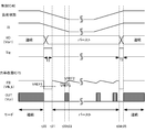
- FIG. 10 is a diagram showing an example of the main waveforms of the IC when transitioning between the “continuous mode” and the “burst mode”.
- FIG. 9 shows a change in the output of the terminal OUT of the power factor improving IC 75 that drives the NMOS transistor 76 when transitioning from “continuous mode” to “burst mode” and from “burst mode” to “continuous mode”. Is shown.
- the power supply device 10 Before time t20, the power supply device 10 is activated, the state of the load 13 becomes a heavy load, and the control IC 40 and the power factor improvement IC 75 operate in the "continuous mode".
- the control IC 40 starts operating in the "burst mode", and the control IC 40 outputs the setting signal Sigma of the "pulse width T3" from the terminal STB.
- the setting signal Sigma is output
- the terminal FB of the power factor improving IC75 becomes the ground voltage
- the power factor improving IC75 sets the terminal OUT to the “L” level, and stops the switching of the NMOS transistor 76.
- the control IC 40 ends the output of the setting signal Sig.
- the voltage Vfb_b of the terminal FB of the power factor improvement IC 75 becomes a feedback voltage corresponding to the output voltage Vout1, and the power factor improvement IC 75 operates in the “burst mode”.
- the power factor improvement IC 75 outputs a drive signal Vdr from the terminal OUT in order to switch the NMOS transistor 76. do.
- the power factor improvement IC 75 stops switching of the comparator transistor 76. , Set the terminal OUT to "L" level.
- the power factor improving IC repeats the same operation and operates in the "burst mode".
- the control IC 40 starts to operate in the "continuous mode", and the control IC 40 outputs the setting signal Sigma of the "pulse width T2" from the terminal STB.
- the setting signal Sigma is output
- the terminal FB of the power factor improving IC75 becomes a ground voltage
- the power factor improving IC75 sets the terminal OUT to the “L” level, and stops switching of the NMOS transistor.
- the control IC 40 ends the output of the setting signal Sig.
- the voltage of the terminal FB becomes the feedback voltage Vfb_b, and the power factor improvement IC 75 operates in the "continuous mode".
- FIG. 11 is a diagram showing an example of the main waveform of the IC in the “short circuit mode”.
- the power factor improvement IC 75 outputs a drive signal Vdr from the terminal OUT in order to switch the NMOS transistor 76. do.
- the power factor improvement IC 75 stops switching of the comparator transistor 76. , Set the terminal OUT to "L" level.
- the power factor improvement IC 75 repeats the same operation as from time t30 to time t32.
- the power factor improvement IC 75 When the power factor improvement IC 75 detects a short-circuit state of the terminal FB at time t35, the power factor improvement IC 75 is in the "short-circuit mode".
- the power factor improving IC 75 recovers from the short-circuited state of the terminal FB, the power factor improving IC 75 operates in the "continuous mode" regardless of the mode before the "short-circuit mode".
- the power supply device 10 of the present embodiment has been described above.
- the signal detection circuit 91 of the power factor improvement IC 75 detects the setting signal Sigma output from the control IC 40 that operates based on the output voltage Vout1 via the terminal FB.
- the terminal FB is a terminal to which a feedback voltage corresponding to the output voltage Vout1 is applied.
- the setting signal Sigma can be detected without using a terminal dedicated to communication. That is, it is possible to provide an integrated circuit in which terminals used for other purposes can be used as terminals for communication with an external circuit.
- the signal detection circuit 91 uses a counter 141 or the like.
- the setting signal Sigma can be detected based on the pulse width. Therefore, the signal detection circuit 91 can realize various operation modes.
- the power factor improving IC 75 operates in a mode based on the setting signal Sigma according to the state of the load 13. ..
- control IC 40 operates the power factor improving IC 75 in the "stop mode", so that the operation of the power supply device 10 is optimized.
- control IC 40 has a circuit for detecting a decrease in the output voltage Vout2 due to a short circuit of the load 13, the control IC 40 can also operate the power factor improving IC 75 in the "stop mode" when a short circuit of the load 13 occurs.
- the setting signal Sigma can be detected based on the change in the voltage of the terminal FB with a simple circuit.
- the setting signal Sigma can be easily detected by changing the voltage Vfb_b of the terminal FB so as to become the ground voltage.
- the detection circuit 131 detects that the terminal FB is short-circuited and short-circuits.
- the power factor improving IC 75 operates in the "continuous mode" and returns in the normal operation. As a result, the power supply device 10 can perform a predetermined operation when recovering from the short circuit of the terminal FB.
- the terminal VH is provided on the power factor improving IC75, even if a terminal dedicated to communication cannot be secured, the power factor improving IC75 can be made smaller by using the terminal FB as a terminal for communication. It is possible to realize a cooperative operation with the control IC 40 while responding to the increase in functions and functions.
Landscapes
- Engineering & Computer Science (AREA)
- Power Engineering (AREA)
- Dc-Dc Converters (AREA)
- Rectifiers (AREA)
Priority Applications (3)
| Application Number | Priority Date | Filing Date | Title |
|---|---|---|---|
| CN202180005468.8A CN114424444A (zh) | 2020-04-15 | 2021-03-04 | 集成电路、电源装置 |
| JP2022515239A JP7279852B2 (ja) | 2020-04-15 | 2021-03-04 | 集積回路、電源装置 |
| US17/703,712 US12068694B2 (en) | 2020-04-15 | 2022-03-24 | Integrated circuit and power supply device |
Applications Claiming Priority (2)
| Application Number | Priority Date | Filing Date | Title |
|---|---|---|---|
| JP2020-072964 | 2020-04-15 | ||
| JP2020072964 | 2020-04-15 |
Related Child Applications (1)
| Application Number | Title | Priority Date | Filing Date |
|---|---|---|---|
| US17/703,712 Continuation US12068694B2 (en) | 2020-04-15 | 2022-03-24 | Integrated circuit and power supply device |
Publications (1)
| Publication Number | Publication Date |
|---|---|
| WO2021210288A1 true WO2021210288A1 (ja) | 2021-10-21 |
Family
ID=78084317
Family Applications (1)
| Application Number | Title | Priority Date | Filing Date |
|---|---|---|---|
| PCT/JP2021/008510 Ceased WO2021210288A1 (ja) | 2020-04-15 | 2021-03-04 | 集積回路、電源装置 |
Country Status (4)
| Country | Link |
|---|---|
| US (1) | US12068694B2 (https=) |
| JP (1) | JP7279852B2 (https=) |
| CN (1) | CN114424444A (https=) |
| WO (1) | WO2021210288A1 (https=) |
Cited By (1)
| Publication number | Priority date | Publication date | Assignee | Title |
|---|---|---|---|---|
| JP2023115577A (ja) * | 2022-02-08 | 2023-08-21 | 富士電機株式会社 | スイッチング制御回路、電源回路 |
Families Citing this family (6)
| Publication number | Priority date | Publication date | Assignee | Title |
|---|---|---|---|---|
| US10897203B2 (en) * | 2019-04-04 | 2021-01-19 | Ambiq Micro, Inc. | Buck converter with inductor sensor |
| US11588408B2 (en) * | 2020-05-06 | 2023-02-21 | Stmicroelectronics S.R.L. | Power supply circuit, corresponding device and method |
| JP7577980B2 (ja) * | 2020-11-27 | 2024-11-06 | 富士電機株式会社 | 電流検出回路、電源回路 |
| JP7746691B2 (ja) * | 2021-05-21 | 2025-10-01 | 富士電機株式会社 | 電源回路、電源装置 |
| JP7749973B2 (ja) * | 2021-08-10 | 2025-10-07 | 富士電機株式会社 | 集積回路、電源回路 |
| IT202200018672A1 (it) * | 2022-09-13 | 2024-03-13 | St Microelectronics Srl | Dispositivo di controllo per un regolatore di tensione a commutazione avente un ridotto rumore audio e metodo di controllo |
Citations (4)
| Publication number | Priority date | Publication date | Assignee | Title |
|---|---|---|---|---|
| JP2011071885A (ja) * | 2009-09-28 | 2011-04-07 | Aiphone Co Ltd | 安定化電源音響出力装置 |
| JP2011147315A (ja) * | 2010-01-18 | 2011-07-28 | Murata Mfg Co Ltd | スイッチング制御回路及びスイッチング電源装置 |
| US20120175958A1 (en) * | 2011-01-11 | 2012-07-12 | American Power Conversion Corporation | Method and apparatus for providing uninterruptible power |
| JP2017060329A (ja) * | 2015-09-17 | 2017-03-23 | 富士電機株式会社 | スイッチング電源装置及びその制御方法 |
Family Cites Families (7)
| Publication number | Priority date | Publication date | Assignee | Title |
|---|---|---|---|---|
| US7952895B2 (en) | 2008-05-29 | 2011-05-31 | Power Integrations, Inc. | Method and apparatus for implementing an unregulated dormant mode in a power converter |
| CN101867295B (zh) * | 2010-03-16 | 2014-07-16 | 成都芯源系统有限公司 | 一种电路及控制方法 |
| CN101867292A (zh) * | 2010-06-17 | 2010-10-20 | 西安交通大学 | 一种基于正激拓扑的远距离供电通信电路 |
| DE112011103261T5 (de) * | 2010-09-28 | 2013-08-22 | Mitsubishi Electric Corporation | Spannungsumformervorrichtung |
| CN103066872B (zh) * | 2013-01-17 | 2015-06-17 | 矽力杰半导体技术(杭州)有限公司 | 一种集成开关电源控制器以及应用其的开关电源 |
| JP6206500B2 (ja) | 2013-10-02 | 2017-10-04 | 株式会社村田製作所 | 電源システム |
| US10910954B1 (en) * | 2019-09-23 | 2021-02-02 | Cypress Semiconductor Corporation | Power saving technique in detach condition for USB-power delivery with integrated synchronous recitifier controller |
-
2021
- 2021-03-04 CN CN202180005468.8A patent/CN114424444A/zh active Pending
- 2021-03-04 WO PCT/JP2021/008510 patent/WO2021210288A1/ja not_active Ceased
- 2021-03-04 JP JP2022515239A patent/JP7279852B2/ja active Active
-
2022
- 2022-03-24 US US17/703,712 patent/US12068694B2/en active Active
Patent Citations (4)
| Publication number | Priority date | Publication date | Assignee | Title |
|---|---|---|---|---|
| JP2011071885A (ja) * | 2009-09-28 | 2011-04-07 | Aiphone Co Ltd | 安定化電源音響出力装置 |
| JP2011147315A (ja) * | 2010-01-18 | 2011-07-28 | Murata Mfg Co Ltd | スイッチング制御回路及びスイッチング電源装置 |
| US20120175958A1 (en) * | 2011-01-11 | 2012-07-12 | American Power Conversion Corporation | Method and apparatus for providing uninterruptible power |
| JP2017060329A (ja) * | 2015-09-17 | 2017-03-23 | 富士電機株式会社 | スイッチング電源装置及びその制御方法 |
Cited By (2)
| Publication number | Priority date | Publication date | Assignee | Title |
|---|---|---|---|---|
| JP2023115577A (ja) * | 2022-02-08 | 2023-08-21 | 富士電機株式会社 | スイッチング制御回路、電源回路 |
| JP7800178B2 (ja) | 2022-02-08 | 2026-01-16 | 富士電機株式会社 | スイッチング制御回路、電源回路 |
Also Published As
| Publication number | Publication date |
|---|---|
| JP7279852B2 (ja) | 2023-05-23 |
| US20220216797A1 (en) | 2022-07-07 |
| US12068694B2 (en) | 2024-08-20 |
| CN114424444A (zh) | 2022-04-29 |
| JPWO2021210288A1 (https=) | 2021-10-21 |
Similar Documents
| Publication | Publication Date | Title |
|---|---|---|
| JP7279852B2 (ja) | 集積回路、電源装置 | |
| US10361633B2 (en) | Control method and device for switching power supplies having more than one control mode | |
| JP7006840B2 (ja) | スイッチング制御回路、電源回路 | |
| US11437913B2 (en) | Switching control circuit and power supply circuit | |
| CN111684697B (zh) | 开关电源装置的控制装置 | |
| JP7749973B2 (ja) | 集積回路、電源回路 | |
| JP7775647B2 (ja) | 集積回路及び電源回路 | |
| CN110401347B (zh) | 直流电源装置 | |
| JP7207576B2 (ja) | 検出回路、スイッチング制御回路、電源回路 | |
| JP7533014B2 (ja) | 集積回路、電源回路 | |
| JP6113527B2 (ja) | Dc/dcコンバータおよびその制御回路、それを用いた電源装置、電源アダプタおよび電子機器 | |
| JP7413805B2 (ja) | スイッチング制御回路、電源回路 | |
| JP7845094B2 (ja) | 集積回路、電源回路 | |
| JP7472654B2 (ja) | スイッチング制御回路、llcコンバータ | |
| JP2023088415A (ja) | 集積回路、及び電源回路 | |
| JP7739878B2 (ja) | スイッチング制御回路、電源回路 | |
| US12431809B2 (en) | Integrated circuit and power supply circuit | |
| JP7823318B2 (ja) | 集積回路、及び電源回路 | |
| JP2025094797A (ja) | スイッチング制御回路、及び電源回路 | |
| CN116915071A (zh) | 集成电路及电源电路 |
Legal Events
| Date | Code | Title | Description |
|---|---|---|---|
| 121 | Ep: the epo has been informed by wipo that ep was designated in this application |
Ref document number: 21789340 Country of ref document: EP Kind code of ref document: A1 |
|
| ENP | Entry into the national phase |
Ref document number: 2022515239 Country of ref document: JP Kind code of ref document: A |
|
| NENP | Non-entry into the national phase |
Ref country code: DE |
|
| 122 | Ep: pct application non-entry in european phase |
Ref document number: 21789340 Country of ref document: EP Kind code of ref document: A1 |