WO2021205941A1 - 三次元アレイ装置 - Google Patents
三次元アレイ装置 Download PDFInfo
- Publication number
- WO2021205941A1 WO2021205941A1 PCT/JP2021/013511 JP2021013511W WO2021205941A1 WO 2021205941 A1 WO2021205941 A1 WO 2021205941A1 JP 2021013511 W JP2021013511 W JP 2021013511W WO 2021205941 A1 WO2021205941 A1 WO 2021205941A1
- Authority
- WO
- WIPO (PCT)
- Prior art keywords
- dimensional array
- array circuit
- layer
- circuit
- wiring group
- Prior art date
- Legal status (The legal status is an assumption and is not a legal conclusion. Google has not performed a legal analysis and makes no representation as to the accuracy of the status listed.)
- Ceased
Links
Images












Classifications
-
- H—ELECTRICITY
- H10—SEMICONDUCTOR DEVICES; ELECTRIC SOLID-STATE DEVICES NOT OTHERWISE PROVIDED FOR
- H10B—ELECTRONIC MEMORY DEVICES
- H10B63/00—Resistance change memory devices, e.g. resistive RAM [ReRAM] devices
- H10B63/30—Resistance change memory devices, e.g. resistive RAM [ReRAM] devices comprising selection components having three or more electrodes, e.g. transistors
-
- H—ELECTRICITY
- H10—SEMICONDUCTOR DEVICES; ELECTRIC SOLID-STATE DEVICES NOT OTHERWISE PROVIDED FOR
- H10B—ELECTRONIC MEMORY DEVICES
- H10B63/00—Resistance change memory devices, e.g. resistive RAM [ReRAM] devices
- H10B63/80—Arrangements comprising multiple bistable or multi-stable switching components of the same type on a plane parallel to the substrate, e.g. cross-point arrays
-
- H—ELECTRICITY
- H10—SEMICONDUCTOR DEVICES; ELECTRIC SOLID-STATE DEVICES NOT OTHERWISE PROVIDED FOR
- H10B—ELECTRONIC MEMORY DEVICES
- H10B61/00—Magnetic memory devices, e.g. magnetoresistive RAM [MRAM] devices
- H10B61/20—Magnetic memory devices, e.g. magnetoresistive RAM [MRAM] devices comprising components having three or more electrodes, e.g. transistors
- H10B61/22—Magnetic memory devices, e.g. magnetoresistive RAM [MRAM] devices comprising components having three or more electrodes, e.g. transistors of the field-effect transistor [FET] type
-
- H—ELECTRICITY
- H10—SEMICONDUCTOR DEVICES; ELECTRIC SOLID-STATE DEVICES NOT OTHERWISE PROVIDED FOR
- H10B—ELECTRONIC MEMORY DEVICES
- H10B63/00—Resistance change memory devices, e.g. resistive RAM [ReRAM] devices
- H10B63/10—Phase change RAM [PCRAM, PRAM] devices
-
- H—ELECTRICITY
- H10—SEMICONDUCTOR DEVICES; ELECTRIC SOLID-STATE DEVICES NOT OTHERWISE PROVIDED FOR
- H10B—ELECTRONIC MEMORY DEVICES
- H10B63/00—Resistance change memory devices, e.g. resistive RAM [ReRAM] devices
- H10B63/80—Arrangements comprising multiple bistable or multi-stable switching components of the same type on a plane parallel to the substrate, e.g. cross-point arrays
- H10B63/84—Arrangements comprising multiple bistable or multi-stable switching components of the same type on a plane parallel to the substrate, e.g. cross-point arrays arranged in a direction perpendicular to the substrate, e.g. 3D cell arrays
-
- H—ELECTRICITY
- H10—SEMICONDUCTOR DEVICES; ELECTRIC SOLID-STATE DEVICES NOT OTHERWISE PROVIDED FOR
- H10D—INORGANIC ELECTRIC SEMICONDUCTOR DEVICES
- H10D30/00—Field-effect transistors [FET]
- H10D30/60—Insulated-gate field-effect transistors [IGFET]
- H10D30/67—Thin-film transistors [TFT]
- H10D30/674—Thin-film transistors [TFT] characterised by the active materials
- H10D30/6755—Oxide semiconductors, e.g. zinc oxide, copper aluminium oxide or cadmium stannate
-
- H—ELECTRICITY
- H10—SEMICONDUCTOR DEVICES; ELECTRIC SOLID-STATE DEVICES NOT OTHERWISE PROVIDED FOR
- H10D—INORGANIC ELECTRIC SEMICONDUCTOR DEVICES
- H10D86/00—Integrated devices formed in or on insulating or conducting substrates, e.g. formed in silicon-on-insulator [SOI] substrates or on stainless steel or glass substrates
- H10D86/40—Integrated devices formed in or on insulating or conducting substrates, e.g. formed in silicon-on-insulator [SOI] substrates or on stainless steel or glass substrates characterised by multiple TFTs
- H10D86/421—Integrated devices formed in or on insulating or conducting substrates, e.g. formed in silicon-on-insulator [SOI] substrates or on stainless steel or glass substrates characterised by multiple TFTs having a particular composition, shape or crystalline structure of the active layer
- H10D86/423—Integrated devices formed in or on insulating or conducting substrates, e.g. formed in silicon-on-insulator [SOI] substrates or on stainless steel or glass substrates characterised by multiple TFTs having a particular composition, shape or crystalline structure of the active layer comprising semiconductor materials not belonging to the Group IV, e.g. InGaZnO
-
- H—ELECTRICITY
- H10—SEMICONDUCTOR DEVICES; ELECTRIC SOLID-STATE DEVICES NOT OTHERWISE PROVIDED FOR
- H10D—INORGANIC ELECTRIC SEMICONDUCTOR DEVICES
- H10D86/00—Integrated devices formed in or on insulating or conducting substrates, e.g. formed in silicon-on-insulator [SOI] substrates or on stainless steel or glass substrates
- H10D86/40—Integrated devices formed in or on insulating or conducting substrates, e.g. formed in silicon-on-insulator [SOI] substrates or on stainless steel or glass substrates characterised by multiple TFTs
- H10D86/441—Interconnections, e.g. scanning lines
-
- H—ELECTRICITY
- H10—SEMICONDUCTOR DEVICES; ELECTRIC SOLID-STATE DEVICES NOT OTHERWISE PROVIDED FOR
- H10D—INORGANIC ELECTRIC SEMICONDUCTOR DEVICES
- H10D86/00—Integrated devices formed in or on insulating or conducting substrates, e.g. formed in silicon-on-insulator [SOI] substrates or on stainless steel or glass substrates
- H10D86/40—Integrated devices formed in or on insulating or conducting substrates, e.g. formed in silicon-on-insulator [SOI] substrates or on stainless steel or glass substrates characterised by multiple TFTs
- H10D86/60—Integrated devices formed in or on insulating or conducting substrates, e.g. formed in silicon-on-insulator [SOI] substrates or on stainless steel or glass substrates characterised by multiple TFTs wherein the TFTs are in active matrices
-
- H—ELECTRICITY
- H10—SEMICONDUCTOR DEVICES; ELECTRIC SOLID-STATE DEVICES NOT OTHERWISE PROVIDED FOR
- H10N—ELECTRIC SOLID-STATE DEVICES NOT OTHERWISE PROVIDED FOR
- H10N70/00—Solid-state devices having no potential barriers, and specially adapted for rectifying, amplifying, oscillating or switching
- H10N70/20—Multistable switching devices, e.g. memristors
- H10N70/231—Multistable switching devices, e.g. memristors based on solid-state phase change, e.g. between amorphous and crystalline phases, Ovshinsky effect
-
- H—ELECTRICITY
- H10—SEMICONDUCTOR DEVICES; ELECTRIC SOLID-STATE DEVICES NOT OTHERWISE PROVIDED FOR
- H10N—ELECTRIC SOLID-STATE DEVICES NOT OTHERWISE PROVIDED FOR
- H10N70/00—Solid-state devices having no potential barriers, and specially adapted for rectifying, amplifying, oscillating or switching
- H10N70/20—Multistable switching devices, e.g. memristors
- H10N70/24—Multistable switching devices, e.g. memristors based on migration or redistribution of ionic species, e.g. anions, vacancies
-
- H—ELECTRICITY
- H10—SEMICONDUCTOR DEVICES; ELECTRIC SOLID-STATE DEVICES NOT OTHERWISE PROVIDED FOR
- H10N—ELECTRIC SOLID-STATE DEVICES NOT OTHERWISE PROVIDED FOR
- H10N70/00—Solid-state devices having no potential barriers, and specially adapted for rectifying, amplifying, oscillating or switching
- H10N70/801—Constructional details of multistable switching devices
- H10N70/821—Device geometry
- H10N70/826—Device geometry adapted for essentially vertical current flow, e.g. sandwich or pillar type devices
-
- H—ELECTRICITY
- H10—SEMICONDUCTOR DEVICES; ELECTRIC SOLID-STATE DEVICES NOT OTHERWISE PROVIDED FOR
- H10N—ELECTRIC SOLID-STATE DEVICES NOT OTHERWISE PROVIDED FOR
- H10N70/00—Solid-state devices having no potential barriers, and specially adapted for rectifying, amplifying, oscillating or switching
- H10N70/801—Constructional details of multistable switching devices
- H10N70/881—Switching materials
- H10N70/883—Oxides or nitrides
- H10N70/8833—Binary metal oxides, e.g. TaOx
-
- Y—GENERAL TAGGING OF NEW TECHNOLOGICAL DEVELOPMENTS; GENERAL TAGGING OF CROSS-SECTIONAL TECHNOLOGIES SPANNING OVER SEVERAL SECTIONS OF THE IPC; TECHNICAL SUBJECTS COVERED BY FORMER USPC CROSS-REFERENCE ART COLLECTIONS [XRACs] AND DIGESTS
- Y02—TECHNOLOGIES OR APPLICATIONS FOR MITIGATION OR ADAPTATION AGAINST CLIMATE CHANGE
- Y02D—CLIMATE CHANGE MITIGATION TECHNOLOGIES IN INFORMATION AND COMMUNICATION TECHNOLOGIES [ICT], I.E. INFORMATION AND COMMUNICATION TECHNOLOGIES AIMING AT THE REDUCTION OF THEIR OWN ENERGY USE
- Y02D10/00—Energy efficient computing, e.g. low power processors, power management or thermal management
Definitions
- One embodiment of the present invention relates to a three-dimensional array device.
- the present invention relates to a three-dimensional array device in which memory cell array circuits are laminated.
- FIG. 30 is a diagram showing a configuration of a general neural network.
- the neuron has an activation function f ( generally referred to as x) for the product-sum operation ⁇ (X i * Wi i ) of N inputs X i (collectively referred to as x) and a weight Wi (collectively referred to as w).
- the input x is multiplied by the neurons of the input layer (Input Layer) and converted into the intermediate output 1.
- the intermediate output 1 is multiplied by the neurons of the hidden layer (Hidden Layer 1) and converted into the intermediate output 2. After similar iterations, it is converted to the final output y by neurons in the output layer (Autoput Layer).
- Non-Patent Document 1 neural networks using non-volatile memory chips based on ReRAM (Resistive Random Access Memory) have been widely studied from the device level to the system level.
- the ReRAM because it has the function of a device called memristor which changes its resistance value by storing the amount of charge flowing through the device, the weight W i of the neural network instead of 0 or 1 binary, it is also possible to control an analog value Is.
- Deep neural networks are expected to be incorporated into various devices as a core technology that supports AI (Artificial Intelligence) applications. Therefore, a binary neural network that can be easily implemented in digital hardware has been proposed.
- the non-volatile memory ReRAM, MRAM, PCRAM or the like can be used.
- a binary neural network based on ReRAM has advantages such as good stability, wide noise margin, and high testability, in addition to being able to use the weights of analog values described above. ..
- the XNOR calculation for weighted sum calculation in a binary neural network can be easily realized as in-memory computing using a ReRAM cell.
- the binary neural network has the demerit that the expressive ability is low because the weight value and the activation value are binarized. Therefore, in a binary neural network, it is common to increase the calculation accuracy by increasing the network size. However, when performing large-scale parallel input / output, there is a problem that a two-dimensional binary neural network causes an increase in footprint. Therefore, at present, research on a three-dimensional neural network in which two-dimensional neural networks are stacked is also being conducted. For example, a device having a 3D laminated structure in which synaptic core layers and interconnect layers are alternately laminated and the layers are connected by through silicon vias (TSVs) has been proposed (Patent Document 1). As described above, by realizing the neural network with the elements of the 3D laminated structure, the area efficiency is improved, and in-memory computing is enabled, so that the power consumption can be reduced.
- TSVs through silicon vias
- the three-dimensional neural network of the prior art needs to be electrically connected by using a method such as TSV or wire bonding via an interconnect layer in order to connect the layers constituting the two-dimensional neural network, and is in the vertical direction. It was difficult to integrate.
- the wiring of the interconnect layer and wire bonding that connects the output terminal of the lower layer neural network and the input terminal of the upper layer neural network becomes long. As a result, signal delay and power consumption increase by that amount.
- One of the problems of the present invention is to provide a three-dimensional array device that realizes a neural network with low latency and low energy loss.
- the three-dimensional array device is a three-dimensional array device having a plurality of layers in the height direction, and includes a first two-dimensional array circuit located in the first layer and the first two-dimensional array device.
- the first two-dimensional array circuit and the second two-dimensional array circuit which are located in a second layer adjacent to the layer and are provided with the first two-dimensional array circuit and a second two-dimensional array circuit that overlaps in a plan view, are provided.
- the two-dimensional array circuit of is a first wiring group, an input unit for inputting a signal to the first wiring group, a second wiring group intersecting with the first wiring group, and a signal from the second wiring group, respectively. It has an output unit for output, and the output unit in the first two-dimensional array circuit is superposed on the input unit in the second two-dimensional array circuit in a plan view and is connected so as to be able to transfer signals.
- the three-dimensional array device is a three-dimensional array device having a plurality of layers in the height direction, and includes a first two-dimensional array circuit located in the first layer and the first two-dimensional array device.
- a second two-dimensional array circuit located in a second layer adjacent to the layer and superimposing on the first two-dimensional array circuit in a plan view, the first two-dimensional array circuit and the second two-dimensional array circuit.
- the two-dimensional array circuit of is a first wiring group, an input unit for inputting a signal to the first wiring group, a second wiring group intersecting with the first wiring group, and a signal from the second wiring group, respectively.
- the second wiring group in the first two-dimensional array circuit is located in the second two-dimensional array circuit and is connected to the input unit in the second two-dimensional array circuit so as to be able to exchange signals. It is substantially parallel to the extending direction of the first wiring group in the two-dimensional array circuit.
- the input unit in the first two-dimensional array circuit does not have to overlap with the output unit in the second two-dimensional array circuit in a plan view.
- the output unit in the first two-dimensional array circuit may be electrically connected to the input unit in the second two-dimensional array circuit via vias.
- the first two-dimensional array circuit and the second two-dimensional array circuit may be a memory cell array circuit.
- the first wiring group may be a wiring group composed of word lines.
- the second wiring group may be a wiring group composed of bit wires.
- the memory cell array circuit may include at least one resistance change type memory and at least one selection transistor in each memory cell.
- the resistance change type memory may have a dielectric layer containing hafnium oxide.
- the selection transistor may have a channel composed of an oxide semiconductor containing IGZO.
- FIG. 3A It is a figure which shows the structure of the 3D array apparatus of 1st Embodiment of this invention. It is a figure which shows the structure of the 2D array circuit of 1st Embodiment. It is a schematic diagram which shows the change of the position of the input part and the output part in a two-dimensional array circuit. It is sectional drawing which shows the structure of the memory cell in the 3D array apparatus of 1st Embodiment. It is an enlarged sectional view which shows the structure of the 3D array apparatus of 1st Embodiment. It is a drawing substitute photograph which shows the layout in the memory cell of the 2D array circuit shown in FIG. 3A. It is a top view which shows typically the layout in the memory cell shown in FIG. FIG.
- FIG. 6 is a drawing-substituting photograph showing a cross-sectional structure in the vicinity of the channel of FET 1 shown in FIG. It is a drawing substitute photograph which shows the cross-sectional structure of ReRAM1 shown in FIG. It is a drawing substitute photograph which shows the layout in the memory cell of the 2D array circuit shown in FIG. 3 (B). It is a drawing substitute photograph which shows the layout in the memory cell of the 2D array circuit shown in FIG. 3C. It is a figure which shows the Id-Vg characteristic of the selection transistor in the 3D array apparatus of 1st Embodiment. It is a figure which shows the Id-Vd characteristic of the selection transistor in the 3D array apparatus of 1st Embodiment.
- a plurality of elements formed by performing a processing treatment such as etching on a certain thin film may have different functions or roles. These plurality of elements are composed of a thin film having the same layer structure and the same material. In the present specification and claims, a plurality of elements formed from thin films having the same layer structure and the same material are referred to as "elements of the same layer”.
- "two two-dimensional array circuits overlap in a plan view" is composed of wiring at both ends of the first wiring group and wiring at both ends of the second wiring group in the two-dimensional array circuit. It means that the quadrilaterals have overlap in the plan view.
- the overlapping area is preferably 50% or more, more preferably 75% or more, and most preferably 95% or more, based on the area of one of the quadrilaterals.
- the input unit and the output unit overlap in a plan view means a quadrilateral having the smallest area including all input terminals included in the input unit and all output terminals included in the output unit. It means that the quadrilateral with the smallest area including has overlap in the plan view.
- the overlapping area is preferably 50% or more, more preferably 75% or more, and most preferably 95% or more, based on the area of one of the quadrilaterals.
- the temperature condition for measurement or simulation is room temperature.
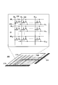
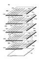
- FIG. 1 is a diagram showing a configuration of a three-dimensional array device 10 according to the first embodiment of the present invention.
- the three-dimensional array device 10 includes a control circuit 100 and two-dimensional array circuits 200a to 200e in this order from the lower layer.
- the control circuit 100 controls each operation (for example, signal input / output) of the two-dimensional array circuits 200a to 200e.
- FIG. 1 shows an example in which a five-layer two-dimensional array circuit is vertically stacked, but the present invention is not limited to this example, and a two-layer or more layer structure can be used.
- the "vertical direction” means a direction perpendicular to the plane constituting the two-dimensional array circuit. Since the three-dimensional array device 10 is a structure in which a plurality of two-dimensional array circuits 200a to 200e are sequentially laminated, the "vertical direction” can be said to be the "height direction” or the "vertical direction”. In the following description, when it is not necessary to distinguish each of the two-dimensional array circuits 200a to 200e, they are collectively referred to as the two-dimensional array circuit 200.
- Each two-dimensional array circuit 200 is a memory cell array circuit based on ReRAM (Resistive Random Access Memory). Specifically, the two-dimensional array circuit 200 has a plurality of memory cells arranged in an array, and each memory cell includes a ReRAM. However, the memory arranged in the memory cell is not limited to ReRAM, and is not limited to ReRAM, but is MRAM (Magnetoristive Random Access Memory), FeRAM (Ferolectric Random Access Memory), PCRAM (Phase Memory), etc. It may be. Further, the two-dimensional array circuit 200 is not limited to the memory cell array circuit, and may be another array type circuit such as a CMOS sensor array circuit.
- ReRAM Resistive Random Access Memory
- each two-dimensional array circuit 200 constitutes a binary neural network (quantized neural network), and a plurality of binary neural networks are laminated to form a deep neural network.
- the two-dimensional array circuit 200a, the two-dimensional array circuits 200b to 200d, and the two-dimensional array circuit 200e are provided with an input layer, a hidden layer, and an output layer (Hidden Layer), respectively.
- a deep neural network with Input Layer may be configured.
- each two-dimensional array circuit 200 has a first wiring group 210, an input unit 215 for inputting a signal to the first wiring group 210, a second wiring group 220 intersecting with the first wiring group 210, and , Has an output unit 225 that outputs a signal from the second wiring group 220.
- the first wiring group 210 is composed of a plurality of word lines.
- the second wiring group 220 is composed of a plurality of bit wires. Memory cells are provided at intersections where word lines and bit lines intersect. That is, although not shown, at least one resistance change memory (ReRAM) and at least one selection transistor are arranged as memory cells at the intersection where the first wiring group 210 and the second wiring group 220 intersect. Will be done.
- the first wiring group 210 is preferably a wiring group composed of wiring parallel to each other.
- the second wiring group 220 is preferably a wiring group composed of wiring parallel to each other, and preferably a wiring group orthogonal to the first wiring group 210.
- the input unit 215 is a portion for inputting information transmitted from an external circuit (including another two-dimensional array circuit 200) to the two-dimensional array circuit 200. Specifically, the information input from the input unit 215 drives each word line constituting the first wiring group 210.
- the input unit 215 is an aggregate of input terminals electrically connected to each word line.
- the output unit 225 is a portion that outputs information from the two-dimensional array circuit 200 to an external circuit (including another two-dimensional array circuit 200).
- the information transmitted via the second wiring group 220 is output via the output unit 225.
- the output unit 225 is an aggregate of output terminals electrically connected to each bit line.
- FIG. 2 is a diagram showing the configuration of the two-dimensional array circuit 200 of the first embodiment.
- the memory cell 230 is arranged at the intersection of the plurality of word lines WL and the plurality of bit lines BL.
- each memory cell 230 is composed of a selection transistor 232 and a resistance change type memory 234.
- the resistance change type memory 234 is provided between the bit line BL and the selection transistor 232.
- the selection transistor 232 is provided between the resistance change memory 234 and the source line SL.
- the word line WL is connected to the gate of the selection transistor 232.
- the configuration of the memory cell 230 is not limited to this example.
- the resistance change memory 234 may be arranged between the selection transistor 232 and the source line SL.
- the two-dimensional array circuit 200 includes peripheral circuits for reading information stored in each memory cell 230 and writing information in each memory cell 230.
- the peripheral circuit may include a peripheral circuit for driving the word line WL and a peripheral circuit for driving the bit line BL. That is, the input unit 215 shown in FIG. 1 may include a peripheral circuit for driving the word line WL. Further, the output unit 225 may include a peripheral circuit for driving the bit line BL.
- These peripheral circuits may include at least one circuit selected from a latch circuit, a buffer circuit, a write circuit, a precharge circuit and an amplifier circuit.
- the peripheral circuit can be formed, for example, by a circuit composed of only n-type IGZO or a CMOS circuit composed of n-type IGZO and p-type SnO. Further, the peripheral circuit may be formed of Si-CMOS on the control circuit 100.
- the resistance change type memory 234 can store 1-bit information by changing the resistance value of the CER layer (hereinafter, also referred to as “resistance change layer”) showing the electric field-induced giant resistance change.
- the information in the low resistance state (Low Resistance State: LRS) where the resistance value is relatively low is set to "0”
- the information in the high resistance state (High Resistance State: HRS) where the resistance value is relatively high is set. Is set to "1".
- LRS Low Resistance State
- HRS High Resistance State
- Each memory cell 230 is individually selected by on / off control of the selection transistor 232.
- the selected memory cell 230 is subjected to an information writing operation or an information reading operation according to the voltages applied to the bit line BL and the source line SL.
- the word line WL is driven based on the signal input to the input unit 215 of the two-dimensional array circuit 200, and the output unit 225 is based on the signal read from the memory cell 230 via the bit line BL.
- the signal output from is determined.
- the two-dimensional array circuit 200a has a first wiring group 210a connected to the input unit 215a and a second wiring group 220a connected to the output unit 225a.
- the two-dimensional array circuit 200b has a first wiring group 210b connected to the input unit 215b and a second wiring group 220b connected to the output unit 225b.
- the two-dimensional array circuit 200c has a first wiring group 210c connected to the input unit 215c and a second wiring group 220c connected to the output unit 225c.
- the two-dimensional array circuit 200d has a first wiring group 210d connected to the input unit 215d and a second wiring group 220d connected to the output unit 225d.
- the two-dimensional array circuit 200e has a first wiring group 210e connected to the input unit 215e and a second wiring group 220e connected to the output unit 225e.
- the three-dimensional array device 10 of the present embodiment has a structure in which two-dimensional array circuits 200a to 200e are stacked while being rotated by 90 degrees from the lower layer to the upper layer. Specifically, in the three-dimensional array device 10, the positions of the input unit 215 and the output unit 225 change by 90 degrees counterclockwise in a plan view. Therefore, in the three-dimensional array device 10 of the present embodiment, the input unit 215 of the two-dimensional array circuit 200 on the upper layer side and the output unit 225 of the two-dimensional array circuit 200 on the lower layer side are superimposed in a plan view.
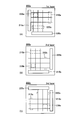
- FIG. 3 is a schematic diagram showing changes in the positions of the input unit 215 and the output unit 225 in the two-dimensional array circuit 200.
- FIGS. 3 (A), 3 (B) and 3 (C) are plan views showing the configurations of the two-dimensional array circuit 200a, the two-dimensional array circuit 200b and the two-dimensional array circuit 200c, respectively. ..
- the two-dimensional array circuit 200b is located at a position in which the two-dimensional array circuit 200a is rotated counterclockwise by 90 degrees in a plan view. In this case, the output unit 225a of the two-dimensional array circuit 200a overlaps with the input unit 215b of the two-dimensional array circuit 200b. Further, as shown in FIGS. 1, 3 (B) and 3 (C), the two-dimensional array circuit 200c is located at a position in which the two-dimensional array circuit 200b is rotated counterclockwise by 90 degrees in a plan view. In this case, the output unit 225b of the two-dimensional array circuit 200b overlaps with the input unit 215c of the two-dimensional array circuit 200c. Although not shown, the relationship between the two-dimensional array circuit 200c and the two-dimensional array circuit 200d and the relationship between the two-dimensional array circuit 200d and the two-dimensional array circuit 200e are the same.
- the positions of the input unit 215 and the output unit 225 change spirally from the lower layer to the upper layer.
- the three-dimensional array device 10 has a structure in which the two-dimensional array circuit on the upper layer side is arranged at a position where the two-dimensional array circuit on the lower layer side is rotated 90 degrees counterclockwise from the lower layer to the upper layer. ..
- the signal input to the three-dimensional array device 10 is calculated while traveling from the lower layer to the upper layer.
- the structure of the three-dimensional array device 10 is not limited to this example.
- the three-dimensional array device 10 has a structure in which the two-dimensional array circuit on the lower layer side is arranged at a position where the two-dimensional array circuit on the upper layer side is rotated 90 degrees clockwise from the upper layer to the lower layer. May be good. That is, the output unit 225 of the two-dimensional array circuit 200 on the upper layer side is electrically connected to the input unit 215 of the two-dimensional array circuit 200 on the lower layer side. In this case, the signal input to the three-dimensional array device 10 is calculated while traveling from the upper layer to the lower layer.
- the output of the two-dimensional array circuit 200 on the lower layer side is the input of the two-dimensional array circuit 200 on the upper layer side. That is, the output unit 225 of the two-dimensional array circuit 200 on the lower layer side is electrically connected to the input unit 215 of the two-dimensional array circuit 200 on the upper layer side.
- any method may be used for the electrical connection between the input unit 215 of the two-dimensional array circuit 200 on the upper layer side and the output unit 225 of the two-dimensional array circuit 200 on the lower layer side.
- an electrical connection method a connection by vias connecting the wiring layers in the previous process, a connection by TSV, or the like may be used.
- the electrical connection between the input unit 215 and the output unit 225 means that the peripheral circuit included in the input unit 215 (peripheral circuit for driving the word line WL, etc.) and the peripheral circuit included in the output unit 225 (peripheral circuit for driving the word line WL, etc.) It includes being electrically connected to (such as a peripheral circuit for driving the bit line BL).
- the output unit 225 of the two-dimensional array circuit 200 on the lower layer side and the input unit 215 of the two-dimensional array circuit 200 on the upper layer side are electrically connected by vias between the wiring layers in the previous process or electrically by TSV. An example of connection is shown, but it is not limited to this example.
- the output unit 225 and the input unit 215 can be separated. It is also possible to connect optically by a silicon through-light interconnection (TSFV). Alternatively, a method in which inductors are provided in the lower layer and the upper layer and wireless radio wave connection by electric field or magnetic field coupling is also possible.
- TSFV silicon through-light interconnection
- the output unit 225 of the two-dimensional array circuit 200 on the lower layer side and the input unit 215 of the two-dimensional array circuit 200 on the upper layer side are superimposed in the vertical direction, so that between the output unit 225 and the input unit 215.
- the wiring length can be minimized. That is, this structure provides a three-dimensional array device 10 that can suppress an increase in signal delay and power consumption due to wiring length as compared with the prior art, and realizes a neural network with low latency and low energy loss. can do.
- FIG. 4 is a cross-sectional view showing the configuration of the memory cell 230 in the three-dimensional array device 10 of the first embodiment.
- the memory cell 230 includes the selection transistor 232 and the resistance change type memory 234.
- the configuration shown in FIG. 4 is an example, and is not limited to this example.
- the substrate 21 functions as a base for supporting the selection transistor 232 and the resistance change memory 234.
- a silicon substrate is used as the substrate 21, but other substrates such as a glass substrate, a resin substrate, a metal substrate, and a ceramics substrate may be used. Further, when the substrate 21 is a silicon substrate, an integrated circuit made of silicon CMOS may be formed.
- the insulating layer 22 functions as a base layer. In the present embodiment, the silicon oxide layer is used as the insulating layer 22, but the present invention is not limited to this example.
- a gate electrode 23 is provided on the insulating layer 22.
- the gate electrode 23 functions as the bottom gate of the selection transistor 232 and also functions as the word line WL shown in FIG.
- the gate electrode 23 has a laminated structure of a first metal layer 23-1 made of titanium (Ti) and a second metal layer 23-2 made of titanium nitride (TiN).
- the film thickness of the first metal layer 23-1 is 5 nm
- the film thickness of the second metal layer 23-2 is 20 nm, but the present invention is not limited to this example.
- the gate electrode 23 may have a single-layer structure or may be configured by using another metal layer.
- the material of the gate electrode 23 a metal material containing tungsten, tantalum, molybdenum, aluminum, copper and the like, or a compound material containing those metal materials may be used.
- the gate electrode 23 can be formed by, for example, a sputtering method.
- Hafnium oxide is used for the gate insulating layer 24.
- the present invention is not limited to this, and a dielectric layer containing an oxide or nitride such as silicon or aluminum may be used as the gate insulating layer 24.
- the gate insulating layer 24 can be formed by using, for example, an ALD (Atomic Layer Deposition) method at a temperature of 250 ° C.
- the film thickness of the gate insulating layer 24 is 8 nm, but the film thickness is not limited to this example.
- the channel layer 25 functions as a channel of the selection transistor 232.
- a metal oxide called IGZO is used as the material constituting the channel layer 25.
- IGZO is a metal oxide exhibiting semiconductor properties, and is a compound material composed of indium, gallium, zinc, and oxygen.
- IGZO is an oxide containing In, Ga and Zn, or a mixture of such oxides.
- the composition of IGZO is preferably In 2-x Ga x O 3 (ZnO) m (0 ⁇ x ⁇ 2, m is a natural number less than 0 or 6), and more preferably InGaO 3 (ZnO) m (m).
- an IGZO film having a film thickness of 8 nm is used as the channel layer 25.
- the IGZO film can be formed by a sputtering method at a temperature of room temperature.
- oxide semiconductors such as oxides containing In, oxides containing Zn, oxides containing Sn, oxides containing In and Zn, oxides containing In and Sn, Sn and Zn are used. Oxides containing, oxides containing In, Sn and Zn, or oxides composed of other elements can also be used as materials constituting the channel layer.
- the gate insulating layer 24 is composed of a dielectric layer
- the channel layer 25 is composed of an IGZO film. Therefore, the formation of an interface layer having a low dielectric constant at the interface between the gate insulating layer 24 and the channel layer 25 is suppressed, and deterioration of transistor characteristics can be suppressed.
- Such an interface layer having a low dielectric constant may be formed between the gate insulating layer 24 and the channel layer 25 when the channel layer is silicon.
- the source electrode 26 and the drain electrode 27 each function as connection terminals for obtaining an electrical connection with the channel layer 25.
- a titanium nitride layer having a film thickness of 20 nm is used as the source electrode 26 and the drain electrode 27.
- the titanium nitride layer can be formed by, for example, a sputtering method.
- the source electrode 26 and the drain electrode 27 may be configured by using other metal materials.
- the functions of the source electrode 26 and the drain electrode 27 may be reversed depending on the voltage applied to each of the source electrode 26 and the drain electrode 27. That is, the source electrode 26 may function as a drain electrode, and the drain electrode 27 may function as a source electrode.
- the drain electrode 27 functions as a lower electrode of the resistance change type memory 234, as will be described later.
- the insulating layer 28 also functions as a flattening layer for flattening the undulations caused by the selection transistor 232.
- the material constituting the insulating layer 28 is not limited to silicon oxide, and other insulating materials (for example, an inorganic material such as silicon nitride or a resin material such as polyimide or acrylic) can be used.
- the insulating layer 28 has an opening 29.
- the opening 29 is provided on the drain electrode 27 and exposes the surface of the drain electrode 27.
- the opening 29 can be formed, for example, by photolithography.
- the diameter of the opening 29 is 3 ⁇ m, but the present invention is not limited to this example.
- a resistance changing layer 30 is provided on the side wall and the bottom of the opening 29.
- the resistance change layer 30 is composed of a dielectric layer containing hafnium oxide, and functions as a CER layer of the resistance change type memory 234.
- the dielectric layer is used as the resistance change layer 30 without patterning, but it may be processed into a pattern covering the opening 29 and used.
- An upper electrode 31 is provided on the resistance change layer 30 so as to cover the opening 29.
- the upper electrode 31 functions as an electrode of the resistance change type memory 234 and also functions as a bit line BL shown in FIG.
- the upper electrode 31 is composed of a metal layer of the same layer as the gate electrode 23 of the selection transistor 232 in the memory cell array circuit on the upper layer side. That is, the upper electrode 31 has a laminated structure of a first metal layer 31-1 made of titanium (Ti) and a second metal layer 31-2 made of titanium nitride (TiN). In this case as well, it can be formed by, for example, a sputtering method, similarly to the gate electrode 23.
- a resistance change type memory 234 composed of a lower electrode (a part of the drain electrode 27), a resistance change layer 30, and an upper electrode 31 is formed inside the opening 29 provided in the insulating layer 28. Will be done.
- the resistance change type memory 234 is connected to the selection transistor 232 via the drain electrode 27.
- the memory cell 230 described above includes a selection transistor 232 having a word line WL as a gate, and a resistance change type memory 234 arranged between the selection transistor 232 and the bit line BL.
- the three-dimensional array device 10 of the present embodiment is configured by stacking memory cell array circuits (two-dimensional array circuits 200) in which the above-mentioned memory cells 230 are arranged in an array.
- the three-dimensional array device 10 has a device structure in which the memory cells 230 shown in FIG. 4 are vertically stacked.
- FIG. 5 is an enlarged cross-sectional view showing the configuration of the three-dimensional array device 10 of the first embodiment. Specifically, it shows a state in which the two-dimensional array circuits 200a to 200c are formed on the substrate 21. As shown in FIG. 5, the two-dimensional array circuits 200a to 200c are laminated on the substrate 21 using a thin film forming process. At this time, the selection transistors 232a to 232c of the two-dimensional array circuits 200a to 200c are separated via the insulating layers 28a to 28c, respectively.
- the upper electrode 31a in the resistance change memory 234a of the two-dimensional array circuit 200a is composed of the same metal layer as the gate electrode 23b in the selection transistor 232b of the two-dimensional array circuit 200b. That is, the upper electrode 31a and the gate electrode 23b are composed of a metal layer having the same structure and the same material. Similarly, the upper electrode 31b in the resistance change memory 234b of the two-dimensional array circuit 200b is composed of the same metal layer as the gate electrode 23c in the selection transistor 232c of the two-dimensional array circuit 200c.
- bit line BL (second wiring group 220) of the lower layer side two-dimensional array circuit 200 and the word line WL (first wiring group 210) of the upper layer side two-dimensional array circuit 200 are It is composed of the same metal layer.
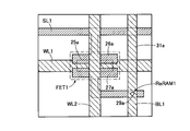
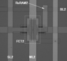
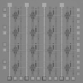
- FIG. 6 is a drawing substitute photograph showing the layout of the two-dimensional array circuit 200a shown in FIG. 3A in the memory cell 230a.
- FIG. 7 is a plan view schematically showing the layout of the memory cell 230a shown in FIG.
- the word line WL1 corresponds to the gate electrode 23a of FIG. 5
- the bit line BL1 corresponds to the upper electrode 31a of FIG.
- the memory cell 230a has the FET 1 and the ReRAM 1 at the intersection of the word line WL1 and the bit line BL1.
- the ReRAM 1 is located inside the opening 29a provided in the insulating layer 28a.
- the circular portion indicated by the arrow corresponds to the opening 29a.
- the present invention is not limited to this example, and the shape of the opening 29a may be polygonal.
- the source line SL1 extends parallel to the word line WL1. As shown in FIG. 7, the source line SL1 is formed integrally with the source electrode 26a of the FET 1 (selection transistor 232a in FIG. 5). Further, the lower electrode of ReRAM 1 (resistance change type memory 234a of FIG. 5) is formed integrally with the drain electrode 27a of FET 1 (selection transistor 232a of FIG. 5).
- the word line WL2 is a wiring formed in the same layer as the bit line BL1 and corresponds to the gate electrode 23b of the selection transistor 232b in FIG.
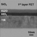
- FIG. 8 is a drawing-substituting photograph showing a cross-sectional structure in the vicinity of the channel of FET 1 shown in FIG. Specifically, FIG. 8 shows a cross-sectional structure in the vicinity of the channel in the selection transistor 232a shown in FIG.
- the titanium nitride layer forming the gate electrode 23a, the dielectric layer containing hafnium oxide forming the gate insulating layer 24a, the IGZO layer forming the channel layer 25a, and the insulating layer 28a are arranged in this order from the lower layer.
- the constituent silicon oxide layer is uniformly formed.
- FIG. 9 is a drawing substitute photograph showing the cross-sectional structure of ReRAM 1 shown in FIG. Specifically, FIG. 9 shows the cross-sectional structure of the resistance change type memory 234a shown in FIG. As shown in FIG. 9, in order from the lower layer, the titanium nitride layer forming the drain electrode 27a, the dielectric layer containing hafnium oxide forming the resistance change layer 30a, and the titanium layer and the titanium nitride layer forming the upper electrode 31a. Is uniformly formed. As will be described later, in the present embodiment, the structure is such that the titanium layer and the dielectric layer containing hafnium oxide are in contact with each other, so that a filament due to oxygen vacancies is formed inside the dielectric layer.
- FIG. 10 is a drawing substitute photograph showing the layout of the two-dimensional array circuit 200b shown in FIG. 3B in the memory cell 230b.
- FIG. 11 is a drawing-substituting photograph showing the layout of the two-dimensional array circuit 200c shown in FIG. 3C in the memory cell 230c.
- the memory cell 230a shown in FIG. 6 is arranged below the memory cell 230b shown in FIG. 10.
- the memory cell 230a shown in FIG. 6 and the memory cell 230b shown in FIG. 10 are arranged in this order from the lower layer.
- the layouts shown in FIGS. 6, 10 and 11 correspond to FIGS. 3 (A), 3 (B) and 3 (C), respectively, and are positioned by rotating 90 degrees counterclockwise in a plan view. It is in a relationship.
- the three-dimensional array device 10 of the present embodiment is configured by stacking a plurality of two-dimensional array circuits 200 (a plurality of memory cell circuits) using a normal thin film forming process.
- the IGZO layer that can be formed at room temperature is used as the channel layer 25 of the selection transistor 232, the three-dimensional array device 10 can be formed by a low temperature process of 400 degrees or less.
- the selection transistor 232 using the IGZO layer as the channel layer 25 has sufficient mobility to drive the memory cell 230. Therefore, according to the present embodiment, it is possible to provide a three-dimensional array device 10 that realizes in-memory computing in an AI application using a deep neural network.
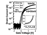
- FIG. 12 is a diagram showing the Id-Vg characteristics of the selection transistors 232a to 232c in the three-dimensional array device 10 of the first embodiment.
- “1st” indicates the characteristics of the selection transistor 232a in the first two-dimensional array circuit 200a shown in FIG.
- “2nd” indicates the characteristics of the selection transistor 232b in the second two-dimensional array circuit 200b shown in FIG.
- “3rd” indicates the characteristics of the selection transistor 232c in the third two-dimensional array circuit 200c shown in FIG.
- the source-drain voltage (Vd) was set to 50 mV or 2 V.
- the channel width and channel length were set to 100 ⁇ m and 10 ⁇ m, respectively.
- FIG. 12 also shows the subthreshold coefficient (SS) obtained from the Id-Vg characteristics.
- SS subthreshold coefficient
- FIG. 13 is a diagram showing Id-Vd characteristics of the selection transistors 232a to 232c in the three-dimensional array device 10 of the first embodiment.
- the meanings of "1st", “2nd” and “3rd” are the same as those in FIG.
- the channel width and channel length were set to 100 ⁇ m and 10 ⁇ m, respectively.
- the gate voltage (Vg) was set to 0.5V, 1V, 1.5V or 2V.
- the selected transistors 232a to 232c all show almost the same transmission characteristics and output characteristics, and no deterioration due to the three-dimensional integration process is observed.
- a drive current of 200 ⁇ A or more was obtained for each of the selection transistors 232a to 232c.
- transistors having a small off current, a large on / off ratio, and a sufficiently large current driving force specifically, a transistor having an IGZO layer as a channel layer.
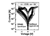
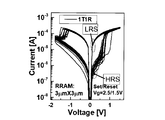
- FIG. 14 shows the IV characteristics of the memory cell composed of the selection transistor 232 and the ReRAM 234 (hereinafter referred to as the “1T1R” cell) and the memory cell composed of only the ReRAM 234 (hereinafter referred to as the “1R” cell). It is a figure which compared with the IV characteristic.
- the IV characteristics of both the "1T1R” cell and the “1R” cell are displayed by superimposing the measurement results of a plurality of times, and show variations between measurement cycles.
- the voltage is applied to the upper electrode 31 with the source electrode 26 grounded, the sweep range of the set / reset voltage of the 1R cell is 1V / -1.5V, and the sweep range of the set / reset voltage of the 1T1R cell is 1.
- ReRAM 234 was set to 3 ⁇ m ⁇ 3 ⁇ m for all memory cells. Further, in the selection transistor 232 of the 1T1R cell, the gate voltage during the set / reset operation was set to 2.5 / 1.5V.
- the on-current of the "1T1R” cell is smaller than the on-current of the "1R” cell.
- the selection transistor 232 connected to the ReRAM 234 acts as a series resistor. Therefore, the reason why the on-current of the "1T1R” cell was measured to be relatively small is considered to be the influence of the series resistance caused by the selection transistor 232.
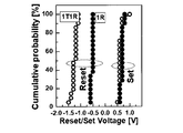
- FIG. 15 is a diagram showing the cumulative probability of the set / reset voltage of the “1T1R” cell and the “1R” cell measured from the IV characteristics shown in FIG.
- FIG. 15 shows the variation between the measurement cycles of the “1T1R” cell and the “1R” cell set / reset voltage.
- the "1T1R” cell showed a reset voltage having a larger absolute value than the "1R” cell.
- the reason for this is that the voltage drop caused by the selection transistor 232 can be ignored because the ReRAM 234 is in a high resistance state at the time of setting, but the series resistance caused by the selection transistor 232 is caused by the ReRAM 234 being in a low resistance state at the time of reset. This is because the resistance of the ReRAM 234 cannot be ignored. Therefore, in order to operate the "1T1R" cell at a low voltage and reduce the area, it is desirable to increase the mobility of the selection transistor 232 and decrease the value of the series resistance.
- FIG. 16 is a diagram in which the IV characteristics of the “1T1R” cell are extracted from the IV characteristics shown in FIG. As shown in FIG. 16, the “1T1R” cell is in a low resistance state in the region indicated by “LRS” and in a high resistance state in the region indicated by “HRS”.
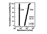
- FIG. 17 is a diagram showing the cumulative probability of resistance values in the low resistance state and the high resistance state of the “1T1R” cell measured from the IV characteristics shown in FIG. FIG. 17 shows the variation between the measurement cycles of the resistance value of the “1T1R” cell. The read voltage was set to 0.1V.
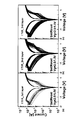
- FIG. 18 is a diagram showing the IV characteristics of the “1T1R” cell in the two-dimensional array circuits 200a to 200c.
- “1st layer”, “2nd layer”, and “3rd layer” mean two-dimensional array circuits 200a to 200c, respectively.
- Each IV characteristic shown in FIG. 18 is a graph obtained by plotting the average value of the results of multiple measurements per single device for 11 devices. That is, the variation in the IV characteristics shown in FIG. 18 indicates the variation between the devices.
- the gate voltage during the set / reset operation was 2.5 / 1.5V. As shown in FIG. 18, no significant difference in IV characteristics was observed between the two-dimensional array circuits 200a to 200c.
- FIG. 19 is a diagram showing the cumulative probabilities of resistance values in the low resistance state and the high resistance state measured from the IV characteristics of the two-dimensional array circuits 200a to 200c shown in FIG.
- FIG. 19 shows the variation of the resistance value of the “1T1R” cell in each layer between devices.
- the read voltage was set to 0.1V. From the results shown in FIG. 19, in the two-dimensional array circuits 200a to 200c, the range in which the ratio of the resistance in the LRS state to the resistance in the HRS state is larger than 10 shows almost the same distribution. From this, it was found that the deterioration of the memory characteristics due to the three-dimensional stacking process was not observed.
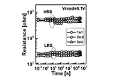
- FIG. 20 is a diagram showing rewrite durability characteristics of each ReRAM of the two-dimensional array circuits 200a to 200c at room temperature.
- the durability characteristics shown in FIG. 20 were measured in a cycle test in which the pulse width was 1 ⁇ s and the Set / Reset voltage was 1 V / ⁇ 1.5 V.
- the deterioration after 105 times of Set / Reset cycle was observed.
- no difference in rewriting durability characteristics was observed among the three layers.
- FIG. 21 is a diagram showing the holding characteristics of the two-dimensional array circuits 200a to 200c in each ReRAM at room temperature, and no deterioration was observed in the ReRAM of each layer after 12 hours.
- no difference in retention characteristics was observed among the three layers.
- FIGS. 20 and 21 no significant difference was observed between the two-dimensional array circuits 200a to 200c, and no decrease in reliability due to three-dimensional integration was observed.
- the present inventors actually prototyped an XNOR circuit using a memory cell 230 (“1T1R” cell) having the structure shown in FIG.
- FIG. 22 is a circuit diagram showing a configuration of an XNOR circuit using two "1T1R" cells.
- FIG. 23 is a photograph showing the configuration of the memory cell array prototyped in the memory cell 230 of the first embodiment.
- FIG. 24 is a photograph showing the configuration of the external peripheral circuit used for the measurement of the prototype XNOR circuit.
- the precharge voltage (V PC ) 0.3 V
- the reference voltage (V REF ) 0.1 V
- the word line voltage (V WL ) 1.5 V.
- the power supply voltage of the external peripheral circuit was set to 3.3V.
- the weight bits (W) are complementarily written to the two ReRAMs.
- the input bit (x) is complementarily applied to the two word lines (WL).
- the capacitor on the bit lines (BL) (V BL) is precharged via the precharge switch (PC).
- the precharged capacitor is discharged at low speed or high speed depending on the given weight bit (W) and input bit (x).
- the voltage of the bit line (BL) is compared with the reference voltage (V REF ) by a comparator (comp.) And binarized to obtain the final output bit (y).
- BL bit line
- FIGS. 4 and 5 show an example in which a bottom gate type transistor is used as the selection transistor 232, the present invention is not limited to this example, and a top gate type transistor may be used.
- FIG. 5 shows an example in which the upper electrode 31 of the lower layer resistance change memory 234 is an element of the same layer as the gate electrode 23 of the upper layer selection transistor 232 adjacent to the lower layer, but these are different layers. It may be an element formed from and separated through an insulating layer.
- FIG. 26 is an enlarged cross-sectional view showing the configuration of the three-dimensional array device 10 in the modified example of the first embodiment. Specifically, it shows a state in which two-dimensional array circuits 200a to 200c having a selection transistor 232 having a top gate structure are formed on a substrate 41. As shown in FIG. 26, the two-dimensional array circuits 200a to 200c are laminated on the substrate 41 using a thin film forming process. At this time, the two-dimensional array circuits 200a to 200c are separated via the insulating layers 43 and 44, respectively.
- silicon oxide is used as the material constituting the insulating layers 43 and 44, but the present invention is not limited to this example, and other insulating materials (for example, an inorganic material such as silicon nitride, or a resin material such as polyimide or acrylic). ) Can be used.
- the substrate 41 is a silicon substrate, and the insulating layer 42 is a silicon oxide layer.
- the same materials as those of the substrate 21 and the insulating layer 22 shown in FIG. 4 can be used.
- the substrate 41 is a silicon substrate, an integrated circuit made of silicon CMOS may be formed.
- FIG. 26 shows an example in which two-dimensional array circuits 200a to 200c are laminated on the substrate 41 and the insulating layer 42 for the sake of simplicity, but in reality, two dimensions are shown on the two-dimensional array circuit 200c.
- the array circuits 200d and 200e are laminated. Since each of the two-dimensional array circuits 200a to 200c has a similar structure, a specific structure of the two-dimensional array circuit 200a will be described in the following description.
- a channel layer 51a, a gate insulating layer 52a, a gate electrode 53a, and a sidewall 54a are provided on the insulating layer 42.
- IGZO, hafnium oxide, tantalum, and silicon oxide are used as materials constituting the channel layer 51a, the gate insulating layer 52a, the gate electrode 53a, and the sidewall 54a, respectively.
- the material constituting the channel layer 51a, the gate insulating layer 52a and the gate electrode 53a the same materials as those of the channel layer 25, the gate insulating layer 24 and the gate electrode 23 shown in FIG. 4 are used. be able to.
- an insulating layer other than silicon oxide may be used as the material constituting the sidewall 54a.
- the gate electrode 53a functions as a top gate of the selection transistor 232 and also functions as a word line WL.
- a source electrode 56a is provided on the channel layer 51a, the gate insulating layer 52a, the gate electrode 53a, and the insulating layer 55a covering the sidewall 54a.
- the source electrode 56a is connected to the channel layer 51a via a contact hole formed in the insulating layer 55a.
- silicon oxide and tantalum nitride are used as the materials constituting the insulating layer 55a and the source electrode 56a, respectively, but the present invention is not limited to this example.
- the source electrode 56a is connected to the source line SL. It is preferable that the gate electrode and the source / drain electrode are self-aligned.
- An insulating layer 57a is provided on the source electrode 56a.
- a via hole penetrating the insulating layer 55a and the insulating layer 57a is formed, and the via 58a is provided inside the via hole.
- tantalum nitride is used as the material constituting the via 58a, but the present invention is not limited to this example.
- the upper surfaces of the insulating layer 57a and the via 58a are flattened by using, for example, CMP (Chemical Mechanical Polishing).
- a resistance change type memory 234a is provided on the insulating layer 57a.
- the resistance change type memory 234a is composed of a lower electrode 59a, a resistance change layer 60a, a first metal layer 61-1a, and a second metal layer 61-2a.
- the laminated electrode composed of the first metal layer 61-1a and the second metal layer 61-2a functions as the upper electrode 61a of the resistance change type memory 234a.
- the materials constituting the lower electrode 59a, the resistance changing layer 60a, the first metal layer 61-1a and the second metal layer 61-2a are titanium nitride, hafnium oxide, titanium and titanium nitride, respectively.
- the present invention is not limited to this example, and the lower electrode 59a and the upper electrode 61a may be made of another metal material, and the resistance change layer 60a may be made of another insulating material. ..
- the resistance change type memory 234a has a structure called a pillar type.
- a pillar-type resistance-changing memory 234a can be formed, for example, by laminating a titanium nitride layer, a hafnium oxide layer, a titanium layer, and a titanium nitride layer in order from the lower layer, and then etching them all at once. ..
- the side surface of the resistance change type memory 234a is covered with the insulating layer 62a.
- the film thickness of the insulating layer 62a can be reduced by CMP or the like until the upper surface of the second metal layer 61-2a is exposed. Just do it.
- the present invention is not limited to this example, and the resistance change type memory 234a may be formed by any method.
- Wiring 63a is provided on the insulating layer 62a.
- the wiring 63a functions as a bit line BL.
- tungsten is used as the material constituting the wiring 63a, but the present invention is not limited to this example.
- the material constituting the wiring 63a the same material as the gate electrode 53a can be used.
- a two-dimensional array circuit 200b is provided on the two-dimensional array circuit 200a having the structure described above via an insulating layer 43.
- the structure of the two-dimensional array circuit 200b is the same as that of the two-dimensional array circuit 200a, and the elements with the same numbers have the same functions.
- the two-dimensional array circuit 200a and the two-dimensional array circuit 200b have a positional relationship rotated by 90 degrees with each other. Therefore, as shown in FIG. 26, the word line WL (gate electrode 53a) of the two-dimensional array circuit 200a is substantially orthogonal to the word line WL (gate electrode 53b) of the two-dimensional array circuit 200b.
- the bit line BL (wiring 63a) of the two-dimensional array circuit 200a is substantially orthogonal to the bit line BL (wiring 3b) of the two-dimensional array circuit 200b.
- the insulating layers 43 and 44 are interposed between the two-dimensional array circuits 200a to 200c. Therefore, for example, the output unit of the two-dimensional array circuit 200a is electrically connected to the input unit of the two-dimensional array circuit 200b via a via (not shown) provided in the insulating layer 43. Similarly, the output portion of the two-dimensional array circuit 200b is electrically connected to the input portion of the two-dimensional array circuit 200c via a via (not shown) provided in the insulating layer 44. As described above, in this modification, the output portion of the two-dimensional array circuit on the lower layer side and the input portion of the two-dimensional array circuit on the upper layer side are electrically connected via vias provided in the insulating layer between the two. Be connected. Therefore, the wiring distance between the output unit of the two-dimensional array circuit on the lower layer side and the input unit of the two-dimensional array circuit on the upper layer side can be shortened, and the effects of wiring delay and energy loss can be suppressed.
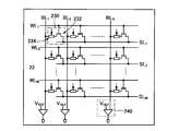
- FIG. 27 is a circuit diagram showing a configuration of a memory cell array circuit that executes arithmetic processing in a digital manner.
- the comparator 240 is arranged at the output end of the bit line BL.
- the comparator 240 is a circuit that outputs a result of comparing the output data of the bit line BL and the reference data (V REF).
- V REF reference data
- a 1-bit digital signal is output according to the output data of the bit line BL input to the comparator 240.
- the two-dimensional array circuit 200 is not limited to the digital system, but can also perform input and output with analog signals and execute arithmetic processing in the analog system.
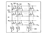
- FIG. 28 is a circuit diagram showing a configuration of a memory cell array circuit that executes arithmetic processing in an analog manner. Specifically, the example shown in FIG. 28 shows a configuration in which a product-sum operation is executed in an analog manner.
- the analog amplifier circuit 250 is arranged at the output end of the bit line BL.
- the analog amplifier circuit 250 outputs the output signal of the bit line BL as an analog signal to output the result of the product-sum calculation.
- the impedance connected between the input terminal and the output terminal may be a resistor (R) or a capacitor (C).
- the analog signal output from the output unit 225 is the input of the upper two-dimensional array circuit 200. It is input to the unit 215.
- the input analog signal can be input to the word line WL as it is, but it can also be A / D converted into a pulse width modulated modulated signal and input to the word line WL. In this way, a signal can be output to the bit line according to the input pulse time of the analog input signal or the modulated signal input to the word line WL and the resistance value of the memory cell 230, and the product-sum calculation can be performed by the analog method. ..
- the three-dimensional array device 10 described in the first embodiment can execute arithmetic processing by either a digital method or an analog method.
- FIG. 29 is a diagram showing the configuration of the three-dimensional array device 10a according to the third embodiment of the present invention.
- the three-dimensional array device 10a includes a control circuit 100 and two-dimensional array circuits 300a to 300e in this order from the lower layer.
- the control circuit 100 controls each operation of the two-dimensional array circuits 300a to 300e.
- FIG. 29 shows an example in which a five-layer two-dimensional array circuit is stacked, but the present invention is not limited to this example, and a two-layer or more layer structure can be used. In the following description, when it is not necessary to distinguish each of the two-dimensional array circuits 300a to 300e, they are collectively referred to as the two-dimensional array circuit 300.
- Each two-dimensional array circuit 300 is a memory cell array circuit based on ReRAM, as in the first embodiment.
- Each of the two-dimensional array circuits 300 is derived from the first wiring group 310, the input unit 315 for inputting a signal to the first wiring group 310, the second wiring group 320 intersecting the first wiring group 310, and the second wiring group 320. It has an output unit 325 that outputs a signal.
- the first wiring group 310 is composed of a plurality of word lines.
- the second wiring group 320 is composed of a plurality of bit wires.
- Memory cells are provided at intersections where word lines and bit lines intersect. That is, although not shown, at least one resistance change memory (ReRAM) and at least one selection transistor are arranged as memory cells at the intersection where the first wiring group 310 and the second wiring group 320 intersect. Will be done.
- ReRAM resistance change memory
- the three-dimensional array device 10a of the present embodiment has a structure in which two-dimensional array circuits 300a to 300e are stacked so that the positions of the input unit 315 and the output unit 325 are switched from the lower layer to the upper layer. Specifically, in the three-dimensional array device 10a, the input units 315 and the output units 325 are alternately arranged in the vertical direction in a plan view. Therefore, in the three-dimensional array device 10a of the present embodiment, the input unit 315 of the two-dimensional array circuit 300 on the upper layer side and the output unit 325 of the two-dimensional array circuit 300 on the lower layer side are superimposed in a plan view.
- the output of the two-dimensional array circuit 300 on the lower layer side is the input of the two-dimensional array circuit 300 on the upper layer side. That is, the output unit 325 of the lower layer side two-dimensional array circuit 300 is electrically connected to the input unit 315 of the upper layer side two-dimensional array circuit 300.
- any method may be used for the electrical connection between the input unit 315 of the two-dimensional array circuit 300 on the upper layer side and the output unit 325 of the two-dimensional array circuit 300 on the lower layer side.
- the output unit 325 of the two-dimensional array circuit 300 on the lower layer side and the input unit 315 of the two-dimensional array circuit 300 on the upper layer side are superimposed in the vertical direction, so that between the output unit 325 and the input unit 315.
- the wiring length can be minimized. That is, this structure provides a three-dimensional array device 10a that can suppress an increase in signal delay and power consumption due to wiring length as compared with the prior art, and realizes a neural network with low latency and low energy loss. can do.
- the output of the two-dimensional array circuit in the front stage and the input of the two-dimensional array circuit in the rear stage are electrically connected. Further, the output portion of the final stage two-dimensional array circuit in the lower layer is superposed in plan view and electrically connected to the input portion of the first two-dimensional array circuit in the adjacent upper layer.
- the values of m and n can be appropriately designed in consideration of an increase in footprint and an increase in cost due to multi-layering.
- comparator 250 ... analog amplifier circuit, 300 ... two-dimensional array circuit, 310 ... first wiring group, 315 ... input section, 320 ... second wiring group, 325 ... output section, 41 ... board, 42 -44 ... Insulation layer, 51a-51c ... Channel layer, 52a-52c ... Gate insulation layer, 53a-53c ... Gate electrode, 54a-54c ... Sidewall, 55a-55c ... Insulation layer, 56a-56c ... Source electrode, 57a -57c ... Insulation layer, 58a-58c ... Via, 59a-59c ... Lower electrode, 60a-60c ... Resistance change layer, 61-1a-61-1c ... First metal layer, 61-2a-61-2c ... Second Metal layer, 61a to 61c ... Upper electrode, 62a to 62c ... Insulation layer, 63a to 63c ... Wiring
Landscapes
- Semiconductor Memories (AREA)
Abstract
三次元アレイ装置は、高さ方向に複数の層を有する三次元アレイ装置であって、第1の層に位置する第1の二次元アレイ回路と、前記第1の層に隣接する第2の層に位置し、前記第1の二次元アレイ回路と平面視において重畳する第2の二次元アレイ回路と、を備え、前記第1の二次元アレイ回路及び前記第2の二次元アレイ回路は、それぞれ、第1配線群、前記第1配線群に信号を入力する入力部、前記第1配線群と交差する第2配線群、及び、前記第2配線群から信号を出力する出力部を有し、前記第1の二次元アレイ回路における前記出力部は、前記第2の二次元アレイ回路における前記入力部と平面視において重畳するとともに信号受け渡し可能に接続される。
Description
本発明の一実施形態は、三次元アレイ装置に関する。特に、メモリセルアレイ回路を積層した三次元アレイ装置に関する。
近年、コンピュータ性能の飛躍的向上及びディープラーニングの発展を背景にして、ニューラルネットワークを多層化したディープニューラルネットワークの研究が進んでいる。図30は、一般的なニューラルネットワークの構成を示す図である。図30において、ニューロンは、N個の入力Xi(xと総称する)と重みWi(wと総称する)との積和演算Σ(Xi*Wi)に対して活性化関数f(k)(k=1,2,...、fと総称する)の非線形演算を行う。ディープニューラルネットワークでは、入力層(Input Layer)のニューロンによって入力xが積和演算されて中間出力1に変換される。中間出力1は、隠れ層(Hidden Layer 1)のニューロンによって積和演算されて中間出力2に変換される。同様の繰り返しの後に、出力層(Output Layer)のニューロンによって最終出力yに変換される。
上記のように、ディープニューラルネットワークにおいては、多量の積和演算を行って誤差を評価し、重みを更新するプロセスを繰り返すことによって学習する。そのため、従来のノイマン型アーキテクチャの半導体チップを使用すると、メモリとCPU又はGPUとの間の通信による消費電力が大きいという課題がある。そこで、ニューロモルフィックコンピューティング、またはインメモリコンピューティングと呼ばれる、非ノイマン型アーキテクチャを採用した不揮発性メモリチップが注目されている。ワード線とビット線の交点に不揮発性メモリ素子を配置したクロスバー構成の2次元アレイ回路においては、各不揮発性メモリに記憶されているデータに対してビット線方向の積和演算結果を出力として読み出すことができる。このようなインメモリコンピューティングの手法は1980年代よりニューラルネットワークのアナログ回路実装において採用されてきた(非特許文献1)。例えば、ReRAM(Resistive Random Access Memory)をベースにした不揮発性メモリチップを用いたニューラルネットワークは、デバイスレベルからシステムレベルに至るまで幅広く研究されている。ReRAMは、素子に流れる電荷量を記憶して抵抗値が変化するメモリスタと呼ばれる素子の機能を有するため、ニューラルネットワークの重みWiを0又は1のバイナリでなく、アナログ値で制御することも可能である。
ディープニューラルネットワークは、AI(Artificial Intelligence)アプリケーションを支える基幹技術として、様々なデバイスに組み込まれることが想定されている。そのため、デジタルハードウェアへの実装が容易なバイナリニューラルネットワークが提案されている。不揮発性メモリとしては、ReRAM、MRAM、又はPCRAM等が使用できる。特に、ReRAMをベースにしたバイナリニューラルネットワークは、先述したアナログ値の重みを使用可能なことに加えて、安定性の良さ、ノイズマージンの広さ、テストの容易性の高さなどの利点を有する。バイナリニューラルネットワークにおける加重和計算(weighted sum calculation)のためのXNOR演算は、ReRAMセルを用いたインメモリコンピューティングとして簡単に実現することができる。
バイナリニューラルネットワークは、重み値と活性化値とを二値化しているため、表現能力が低いというデメリットを有する。そのため、バイナリニューラルネットワークは、ネットワークサイズを大きくすることにより演算精度を上げることが一般的である。しかしながら、大規模な並列入出力を行う場合、二次元のバイナリニューラルネットワークでは、フットプリントの増加を招くという問題がある。そのため、現在では、二次元ニューラルネットワークを積層した三次元ニューラルネットワークの研究も行われている。例えば、シナプティックコア層とインターコネクト層とを交互に積層して、層間をシリコン貫通電極(TSV)で接続した3D積層構造の素子が提案されている(特許文献1)。このように、ニューラルネットワークを3D積層構造の素子で実現することにより、面積効率が向上するとともに、インメモリコンピューティングを可能とすることにより低消費電力化が可能となる。
森江隆、「ニューロモルフィックシステムと物理デバイス」、応用物理、社団法人応用物理学会、2019年、第88巻、第7号、p.481-485
従来技術の三次元ニューラルネットワークは、二次元ニューラルネットワークを構成する層間を接続するために、インターコネクト層を介したTSVやワイヤボンディング等の手法を用いて電気的に連結する必要があり、垂直方向の集積化が困難であった。また、インメモリコンピューティング用の不揮発性メモリチップを三次元方向に積層する場合、下層のニューラルネットワークの出力端子と上層のニューラルネットワークの入力端子とを接続するインターコネクト層やワイヤボンディングの配線が長くなると、その分だけ信号遅延や消費電力の増加を招く結果となっていた。
本発明の課題の一つは、低レイテンシで低エネルギー損失のニューラルネットワークを実現する三次元アレイ装置を提供することにある。
本発明の一実施形態における三次元アレイ装置は、高さ方向に複数の層を有する三次元アレイ装置であって、第1の層に位置する第1の二次元アレイ回路と、前記第1の層に隣接する第2の層に位置し、前記第1の二次元アレイ回路と平面視において重畳する第2の二次元アレイ回路と、を備え、前記第1の二次元アレイ回路及び前記第2の二次元アレイ回路は、それぞれ、第1配線群、前記第1配線群に信号を入力する入力部、前記第1配線群と交差する第2配線群、及び、前記第2配線群から信号を出力する出力部を有し、前記第1の二次元アレイ回路における前記出力部は、前記第2の二次元アレイ回路における前記入力部と平面視において重畳するとともに信号受け渡し可能に接続される。
本発明の一実施形態における三次元アレイ装置は、高さ方向に複数の層を有する三次元アレイ装置であって、第1の層に位置する第1の二次元アレイ回路と、前記第1の層に隣接する第2の層に位置し、前記第1の二次元アレイ回路と平面視において重畳する第2の二次元アレイ回路と、を備え、前記第1の二次元アレイ回路及び前記第2の二次元アレイ回路は、それぞれ、第1配線群、前記第1配線群に信号を入力する入力部、前記第1配線群と交差する第2配線群、及び、前記第2配線群から信号を出力する出力部を有し、前記第1の二次元アレイ回路における前記出力部は、前記第2の二次元アレイ回路における前記出力部よりも前記第2の二次元アレイ回路における前記入力部の近くに位置するとともに、前記第2の二次元アレイ回路における前記入力部と信号受け渡し可能に接続され、前記第1の二次元アレイ回路における前記第2配線群が延在する方向は、前記第2の二次元アレイ回路における前記第1配線群が延在する方向と略平行である。
前記第1の二次元アレイ回路における前記入力部は、前記第2の二次元アレイ回路における前記出力部と平面視において重畳しなくてもよい。
前記第1の二次元アレイ回路における前記出力部は、前記第2の二次元アレイ回路における前記入力部とビアを介して電気的に接続されてもよい。
前記第1の二次元アレイ回路及び前記第2の二次元アレイ回路は、メモリセルアレイ回路であってもよい。この場合、前記第1配線群は、ワード線で構成される配線群であってもよい。前記第2配線群は、ビット線で構成される配線群であってもよい。
前記メモリセルアレイ回路は、各メモリセルに、少なくとも1つの抵抗変化型メモリと少なくとも1つの選択トランジスタとを含んでもよい。このとき、前記抵抗変化型メモリは、酸化ハフニウムを含む誘電体層を有していてもよい。前記選択トランジスタは、IGZOを含む酸化物半導体で構成されるチャネルを有していてもよい。
以下、本発明の実施形態について、図面等を参照しつつ説明する。但し、本発明は、その要旨を逸脱しない範囲において様々な態様で実施することができ、以下に例示する実施形態の記載内容に限定して解釈されるものではない。図面は、説明をより明確にするため、実際の態様に比べ、各部の幅、厚さ、形状等について模式的に表される場合があるが、あくまで一例であって、本発明の解釈を限定するものではない。本明細書と各図面において、既出の図面に関して説明したものと同様の機能を備えた要素には、同一の符号を付して、重複する説明を省略することがある。
本明細書において、ある1つの薄膜に対してエッチング等の加工処理を行うことにより形成された複数の要素(element)は、それぞれ異なる機能又は役割を有する場合がある。これらの複数の要素は、同一の層構造及び同一の材料の薄膜から構成される。本明細書及び特許請求の範囲では、同一の層構造及び同一の材料の薄膜から形成される複数の要素を「同一層の要素」と呼ぶ。
本明細書において、「2つの二次元アレイ回路が平面視において重畳する」とは、該二次元アレイ回路において、第1配線群の両端の配線と第2の配線群の両端の配線によって構成される四辺形が平面視において重なりを有することを意味する。重なる面積はいずれか片方の四辺形の面積を基準として50%以上が好ましく75%以上がより好ましく95%以上が最も好ましい。
本明細書において、「2つの二次元アレイ回路が平面視において重畳する」とは、該二次元アレイ回路において、第1配線群の両端の配線と第2の配線群の両端の配線によって構成される四辺形が平面視において重なりを有することを意味する。重なる面積はいずれか片方の四辺形の面積を基準として50%以上が好ましく75%以上がより好ましく95%以上が最も好ましい。
本明細書において、「入力部と出力部が平面視において重畳する」とは、該入力部に含まれるすべての入力端子を含む最小面積の四辺形と該出力部に含まれるすべての出力端子を含む最小面積の四辺形が平面視において重なりを有することを意味する。重なる面積はいずれか片方の四辺形の面積を基準として50%以上が好ましく75%以上がより好ましく95%以上が最も好ましい。入力端子と出力端子とが垂直に接続される場合、例えば、シリコン貫通電極によるビア接続の場合は、100%が平面視において重畳することになる。
本明細書において、図面に示した要素を説明する際には、その要素に付した符号を用いて説明を行う。このとき、同様の機能を備えた複数の要素については、同一の符号にアルファベット等の記号(例えば、「a」、「b」等)を付して区別する場合がある。しかしながら、各要素を区別して説明する必要がないときは、その要素を示す符号のみを用いて説明する場合がある。
以下に説明する各実施形態において、測定又はシミュレーションの温度条件は、いずれも室温である。
(第1実施形態)
[三次元アレイ装置の構造]
図1は、本発明の第1実施形態の三次元アレイ装置10の構成を示す図である。図1に示すように、三次元アレイ装置10は、下層から順に、制御回路100、及び、二次元アレイ回路200a~200eを含む。制御回路100は、二次元アレイ回路200a~200eの各動作(例えば、信号の入出力)を制御する。図1では、5層の二次元アレイ回路を垂直方向に重ねた例を示すが、この例に限られるものではなく、2層以上の層構造とすることができる。ここで「垂直方向」とは、二次元アレイ回路を構成する平面に対して垂直な方向をいう。三次元アレイ装置10は、複数の二次元アレイ回路200a~200eを順次積層した構造体であるため、「垂直方向」は、「高さ方向」又は「上下方向」とも言える。以下の説明において、各二次元アレイ回路200a~200eを区別する必要がない場合は、二次元アレイ回路200と総称する。
各二次元アレイ回路200は、ReRAM(Resistive Random Access Memory)をベースとしたメモリセルアレイ回路である。具体的には、二次元アレイ回路200は、アレイ状に配置された複数のメモリセルを有し、各メモリセルにReRAMを含む。ただし、メモリセルに配置されるメモリは、ReRAMに限られるものではなく、MRAM(Magnetoresistive Random Access Memory)、FeRAM(Ferroelectric Random Access Memory)、PCRAM(Phase Change Random Access Memory)など、他の不揮発性メモリであってもよい。また、二次元アレイ回路200は、メモリセルアレイ回路に限らず、CMOSセンサアレイ回路などの他のアレイ型回路であってもよい。
本実施形態では、三次元アレイ装置10を用いてインメモリコンピューティングを実現する。具体的には、各二次元アレイ回路200によりバイナリニューラルネットワーク(量子化されたニューラルネットワーク)を構成し、複数のバイナリニューラルネットワークを積層してディープニューラルネットワークを構成する。例えば、三次元アレイ装置10は、二次元アレイ回路200a、二次元アレイ回路200b~200d、並びに、二次元アレイ回路200eを、それぞれ入力層(Input Layer)、隠れ層(Hidden Layer)及び出力層(Output Layer)としたディープニューラルネットワークを構成してもよい。
図1に示すように、各二次元アレイ回路200は、第1配線群210、第1配線群210に信号を入力する入力部215、第1配線群210と交差する第2配線群220、及び、第2配線群220から信号を出力する出力部225を有する。本実施形態において、第1配線群210は、複数のワード線で構成される。第2配線群220は、複数のビット線で構成される。メモリセルは、ワード線とビット線とが交差する交点に設けられる。すなわち、図示は省略するが、第1配線群210と第2配線群220とが交差する交差部には、メモリセルとして、少なくとも1つの抵抗変化型メモリ(ReRAM)と少なくとも1つの選択トランジスタが配置される。第1配線群210は、互いに平行な配線からなる配線群であることが好ましい。第2配線群220は、互いに平行な配線からなる配線群であることが好ましく、第1配線群210と互いに直交する配線群であることが好ましい。
入力部215は、外部回路(他の二次元アレイ回路200を含む)から伝達された情報を二次元アレイ回路200に入力する部位である。具体的には、入力部215から入力された情報は、第1配線群210を構成する各ワード線を駆動する。本実施形態において、入力部215は、各ワード線に電気的に接続された入力端子の集合体である。出力部225は、二次元アレイ回路200から外部回路(他の二次元アレイ回路200を含む)に情報を出力する部位である。具体的には、第2配線群220を介して伝達された情報が出力部225を経由して出力される。本実施形態において、出力部225は、各ビット線に電気的に接続された出力端子の集合体である。
図2は、第1実施形態の二次元アレイ回路200の構成を示す図である。図2に示すように、複数のワード線WLと複数のビット線BLとの交差部には、メモリセル230が配置される。本実施形態では、各メモリセル230は、選択トランジスタ232と抵抗変化型メモリ234とで構成される。抵抗変化型メモリ234は、ビット線BLと選択トランジスタ232との間に設けられる。選択トランジスタ232は、抵抗変化型メモリ234とソース線SLとの間に設けられる。ワード線WLは、選択トランジスタ232のゲートに接続される。ただし、メモリセル230の構成は、この例に限られるものではない。例えば、抵抗変化型メモリ234は、選択トランジスタ232とソース線SLとの間に配置されてもよい。
図2では図示を省略するが、二次元アレイ回路200は、各メモリセル230に記憶した情報を読み出したり、各メモリセル230に情報を書き込んだりするための周辺回路を備えている。周辺回路は、ワード線WLを駆動するための周辺回路とビット線BLを駆動するための周辺回路とを含んでもよい。すなわち、図1に示す入力部215は、ワード線WLを駆動するための周辺回路を含んでもよい。また、出力部225は、ビット線BLを駆動するための周辺回路を含んでもよい。これらの周辺回路は、ラッチ回路、バッファ回路、書き込み回路、プリチャージ回路及びアンプ回路から選択された少なくとも1つの回路を含んでもよい。該周辺回路は、例えばn型のIGZOのみからなる回路や、n型のIGZOとp型のSnOからなるCMOS回路で形成できる。また、周辺回路は、制御回路100上にSi-CMOSで形成しても良い。
抵抗変化型メモリ234は、電界誘起巨大抵抗変化を示すCER層(以下、「抵抗変化層」ともいう。)の抵抗値を変化させることにより、1ビットの情報を記憶することができる。例えば、抵抗値が相対的に低い低抵抗状態(Low Resistance State:LRS)のときの情報を「0」とし、抵抗値が相対的に高い高抵抗状態(High Resistance State:HRS)のときの情報を「1」とする。ただし、該抵抗値と「0」又は「1」の情報との対応関係は逆であってもよい。
各メモリセル230は、選択トランジスタ232のオン/オフ制御により個々に選択される。選択されたメモリセル230は、ビット線BL及びソース線SLに印加された電圧に応じて、情報の書き込み動作又は読み出し動作が行われる。本実施形態では、二次元アレイ回路200の入力部215に入力された信号に基づいてワード線WLが駆動され、ビット線BLを介してメモリセル230から読み出された信号に基づいて出力部225から出力される信号が決定される。
図1に説明を戻す。二次元アレイ回路200aは、入力部215aに接続された第1配線群210a及び出力部225aに接続された第2配線群220aを有する。二次元アレイ回路200bは、入力部215bに接続された第1配線群210b及び出力部225bに接続された第2配線群220bを有する。二次元アレイ回路200cは、入力部215cに接続された第1配線群210c及び出力部225cに接続された第2配線群220cを有する。二次元アレイ回路200dは、入力部215dに接続された第1配線群210d及び出力部225dに接続された第2配線群220dを有する。二次元アレイ回路200eは、入力部215eに接続された第1配線群210e及び出力部225eに接続された第2配線群220eを有する。
本実施形態の三次元アレイ装置10は、下層から上層に向かって、90度ずつ回転させながら二次元アレイ回路200a~200eを重ねた構造を有する。具体的には、三次元アレイ装置10は、平面視において、左回りに90度ずつ入力部215及び出力部225の位置が変化する。そのため、本実施形態の三次元アレイ装置10は、上層側の二次元アレイ回路200の入力部215と、下層側の二次元アレイ回路200の出力部225とが平面視において重畳する。
図3は、二次元アレイ回路200における入力部215及び出力部225の位置の変化を示す模式図である。具体的には、図3(A)、図3(B)及び図3(C)は、それぞれ二次元アレイ回路200a、二次元アレイ回路200b及び二次元アレイ回路200cの構成を示す平面図である。
図1、図3(A)及び図3(B)に示すように、二次元アレイ回路200bは、平面視において二次元アレイ回路200aを左回りに90度回転させた位置にある。この場合、二次元アレイ回路200aの出力部225aは、二次元アレイ回路200bの入力部215bと重畳する。また、図1、図3(B)及び図3(C)に示すように、二次元アレイ回路200cは、平面視において二次元アレイ回路200bを左回りに90度回転させた位置にある。この場合、二次元アレイ回路200bの出力部225bは、二次元アレイ回路200cの入力部215cと重畳する。図示は省略するが、二次元アレイ回路200cと二次元アレイ回路200dとの関係、及び、二次元アレイ回路200dと二次元アレイ回路200eとの関係も同様である。
以上のように、本実施形態の三次元アレイ装置10は、下層から上層に向かって、入力部215及び出力部225の位置が螺旋状に変化する。具体的には、三次元アレイ装置10は、下層から上層に向かって、下層側の二次元アレイ回路を左回りに90度回転させた位置に上層側の二次元アレイ回路を配置した構造を有する。この場合、三次元アレイ装置10に入力された信号は、下層から上層に向かって進みながら演算される。ただし、三次元アレイ装置10の構造は、この例に限られるものではない。例えば、三次元アレイ装置10は、上層から下層に向かって、上層側の二次元アレイ回路を右回りに90度回転させた位置に下層側の二次元アレイ回路を配置した構造を有していてもよい。すなわち、上層側の二次元アレイ回路200の出力部225は、下層側の二次元アレイ回路200の入力部215と電気的に接続されている。この場合、三次元アレイ装置10に入力された信号は、上層から下層に向かって進みながら演算される。
また、図1において矢印で示すように、下層側の二次元アレイ回路200の出力は、上層側の二次元アレイ回路200の入力となる。すなわち、下層側の二次元アレイ回路200の出力部225は、上層側の二次元アレイ回路200の入力部215と電気的に接続されている。このとき、上層側の二次元アレイ回路200の入力部215と下層側の二次元アレイ回路200の出力部225との間の電気的な接続は、如何なる方法を用いてもよい。例えば、電気的な接続方法として、前工程の配線層間を接続するビアによる接続や、TSVによる接続などを用いてもよい。また、入力部215と出力部225とが電気的に接続することは、入力部215に含まれる周辺回路(ワード線WLを駆動するための周辺回路など)と出力部225に含まれる周辺回路(ビット線BLを駆動するための周辺回路など)とが電気的に接続されることを含む。なお、ここでは下層側の二次元アレイ回路200の出力部225と上層側の二次元アレイ回路200の入力部215とを、前工程の配線層間のビアによる電気的な接続やTSVによる電気的な接続の例を示したが、この例に限られるものではない。例えば、下層側の二次元アレイ回路200の出力部225に面発光レーザを設け、上層側の二次元アレイ回路200の入力部215に受光素子を設けることにより、出力部225と入力部215とをシリコン貫通光インターコネクション(TSFV)により光学的に接続することも可能である。あるいは、下層と上層にインダクタを設けて電界または磁界結合による無線電波接続による方法も可能である。
本実施形態では、下層側の二次元アレイ回路200の出力部225と上層側の二次元アレイ回路200の入力部215とが垂直方向に重畳するため、出力部225と入力部215との間の配線長を最小限に抑えることができる。すなわち、この構造により、従来技術に比べて、配線長に起因する信号遅延や消費電力の増加を抑制することができ、低レイテンシで低エネルギー損失なニューラルネットワークを実現する三次元アレイ装置10を提供することができる。
[メモリセルの構成]
図4は、第1実施形態の三次元アレイ装置10におけるメモリセル230の構成を示す断面図である。前述のとおり、本実施形態において、メモリセル230は、選択トランジスタ232及び抵抗変化型メモリ234を含む。ただし、図4に示す構成は一例であり、この例に限られるものではない。
図4は、第1実施形態の三次元アレイ装置10におけるメモリセル230の構成を示す断面図である。前述のとおり、本実施形態において、メモリセル230は、選択トランジスタ232及び抵抗変化型メモリ234を含む。ただし、図4に示す構成は一例であり、この例に限られるものではない。
図4において、基板21は、選択トランジスタ232及び抵抗変化型メモリ234を支持するベースとして機能する。本実施形態では、基板21として、シリコン基板を用いるが、ガラス基板、樹脂基板、金属基板、セラミックス基板等の他の基板を用いてもよい。また、基板21がシリコン基板の場合、シリコンCMOSによる集積回路が形成されていてもよい。絶縁層22は、下地層として機能する。本実施形態では、絶縁層22として酸化シリコン層を用いるが、この例に限られるものではない。
絶縁層22の上には、ゲート電極23が設けられる。ゲート電極23は、選択トランジスタ232のボトムゲートとして機能するとともに、図2に示したワード線WLとして機能する。ゲート電極23は、チタン(Ti)で構成される第1金属層23-1と窒化チタン(TiN)で構成される第2金属層23-2との積層構造を有する。本実施形態では、第1金属層23-1の膜厚を5nmとし、第2金属層23-2の膜厚を20nmとするが、この例に限られるものではない。また、ゲート電極23は、単層構造であってもよいし、他の金属層を用いて構成してもよい。例えば、ゲート電極23の材料としては、タングステン、タンタル、モリブデン、アルミニウム、銅等を含む金属材料、又は、それらの金属材料を含む化合物材料を用いてもよい。ゲート電極23は、例えばスパッタ法により形成することができる。
ゲート絶縁層24は、酸化ハフニウムを用いる。ただし、これに限らず、ゲート絶縁層24として、シリコン、アルミニウム等の酸化物又は窒化物を含む誘電体層を用いても良い。ゲート絶縁層24は、例えば250℃の温度下におけるALD(Atomic Layer Deposition)法を用いて形成することができる。本実施形態では、ゲート絶縁層24の膜厚は8nmとするが、この例に限られるものではない。
チャネル層25は、選択トランジスタ232のチャネルとして機能する。本実施形態では、チャネル層25を構成する材料として、IGZOと呼ばれる金属酸化物を用いる。IGZOは、半導体特性を示す金属酸化物であり、インジウム、ガリウム、亜鉛、及び酸素で構成される化合物材料である。具体的には、IGZOは、In、Ga及びZnを含む酸化物、又は、このような酸化物の混合物である。IGZOの組成は、好ましくは、In2-xGaxO3(ZnO)m(0<x<2、mは、0又は6未満の自然数)、より好ましくは、InGaO3(ZnO)m(mは、0又は6未満の自然数)、最も好ましくは、InGaO3(ZnO)である。本実施形態では、チャネル層25として、8nmの膜厚のIGZO膜を用いる。IGZO膜は、室温の温度下におけるスパッタ法により形成することができる。IGZOに代えて、他の酸化物半導体、例えばInを含む酸化物、Znを含む酸化物、Snを含む酸化物、InとZnを含む酸化物、InとSnを含む酸化物、SnとZnを含む酸化物、InとSnとZnを含む酸化物、あるいはその他の元素からなる酸化物を、チャネル層を構成する材料として使用することもできる。
本実施形態では、ゲート絶縁層24が誘電体層で構成され、チャネル層25がIGZO膜で構成される。そのため、ゲート絶縁層24とチャネル層25との界面における誘電率の低い界面層の形成が抑制され、トランジスタ特性の劣化を抑制することができる。このような誘電率の低い界面層は、チャネル層がシリコンである場合にゲート絶縁層24とチャネル層25との間に形成される場合がある。
ソース電極26及びドレイン電極27は、それぞれチャネル層25との電気的な接続を得るための接続端子として機能する。本実施形態では、ソース電極26及びドレイン電極27として、20nmの膜厚の窒化チタン層を用いる。窒化チタン層は、例えばスパッタ法により形成することができる。ただし、この例に限らず、ソース電極26及びドレイン電極27は、他の金属材料を用いて構成してもよい。なお、ソース電極26及びドレイン電極27は、それぞれに印加される電圧に応じて、機能が逆になる場合もある。すなわち、ソース電極26がドレイン電極として機能し、ドレイン電極27がソース電極として機能する場合がある。なお、ドレイン電極27は、後述するように、抵抗変化型メモリ234の下部電極として機能する。
選択トランジスタ232は、絶縁層28で覆われている。本実施形態において、絶縁層28は、200nmの膜厚の酸化シリコン層である。絶縁層28は、例えばプラズマCVD法又はスパッタ法により形成することができる。後述するように、本実施形態の三次元アレイ装置10は、複数のメモリセルアレイ回路を積層した構造を有する。そのため、絶縁層28は、下層側のメモリセルアレイ回路と上層側のメモリセルアレイ回路とを絶縁分離する機能を有する。また、絶縁層28は、選択トランジスタ232のチャネル層25を水分等から保護するパッシベーション層としても機能する。さらに、絶縁層28は、選択トランジスタ232に起因する起伏を平坦化する平坦化層としても機能する。ただし、絶縁層28を構成する材料は、酸化シリコンに限らず、他の絶縁材料(例えば、窒化シリコン等の無機材料、又は、ポリイミド、アクリル等の樹脂材料)を用いることができる。
絶縁層28は、開口部29を有する。開口部29は、ドレイン電極27の上に設けられ、ドレイン電極27の表面を露出させる。開口部29は、例えばフォトリソグラフィにより形成することができる。本実施形態では、開口部29の径を3μmとするが、この例に限られるものではない。
開口部29の側壁及び底部には、抵抗変化層30が設けられる。抵抗変化層30は、酸化ハフニウムを含む誘電体層で構成され、抵抗変化型メモリ234のCER層として機能する。本実施形態では、抵抗変化層30として誘電体層をパターニングせずに用いているが、開口部29を覆うパターンに加工して用いてもよい。
抵抗変化層30の上には、開口部29を覆うように上部電極31が設けられる。上部電極31は、抵抗変化型メモリ234の電極として機能するとともに、図2に示したビット線BLとして機能する。本実施形態において、上部電極31は、上層側のメモリセルアレイ回路における選択トランジスタ232のゲート電極23と同一層の金属層で構成される。すなわち、上部電極31は、チタン(Ti)で構成される第1金属層31-1と窒化チタン(TiN)で構成される第2金属層31-2との積層構造を有する。この場合も、ゲート電極23と同様に、例えばスパッタ法により形成することができる。
以上のように、絶縁層28に設けられた開口部29の内側には、下部電極(ドレイン電極27の一部)、抵抗変化層30及び上部電極31で構成される抵抗変化型メモリ234が形成される。抵抗変化型メモリ234は、ドレイン電極27を介して選択トランジスタ232に接続される。以上説明したメモリセル230は、図2に示したとおり、ワード線WLをゲートとする選択トランジスタ232と、選択トランジスタ232とビット線BLとの間に配置された抵抗変化型メモリ234とを含む。
本実施形態の三次元アレイ装置10は、上述したメモリセル230をアレイ状に配置したメモリセルアレイ回路(二次元アレイ回路200)を積層することにより構成されている。具体的には、三次元アレイ装置10は、図4に示したメモリセル230を垂直方向に積層したデバイス構造を有する。
図5は、第1実施形態の三次元アレイ装置10の構成を示す拡大断面図である。具体的には、基板21上に、二次元アレイ回路200a~200cまでを形成した状態を示している。図5に示すように、二次元アレイ回路200a~200cは、薄膜形成プロセスを用いて基板21上に積層される。このとき、各二次元アレイ回路200a~200cの選択トランジスタ232a~232cは、それぞれ絶縁層28a~28cを介して分離される。
また、図5に示すように、二次元アレイ回路200aの抵抗変化型メモリ234aにおける上部電極31aは、二次元アレイ回路200bの選択トランジスタ232bにおけるゲート電極23bと同一層の金属層で構成される。すなわち、上部電極31aとゲート電極23bとは、同一構造かつ同一材料の金属層で構成される。同様に、二次元アレイ回路200bの抵抗変化型メモリ234bにおける上部電極31bは、二次元アレイ回路200cの選択トランジスタ232cにおけるゲート電極23cと同一層の金属層で構成される。換言すれば、本実施形態では、下層側の二次元アレイ回路200のビット線BL(第2配線群220)と上層側の二次元アレイ回路200のワード線WL(第1配線群210)とが同一層の金属層で構成される。
図6は、図3(A)に示した二次元アレイ回路200aのメモリセル230aにおけるレイアウトを示す図面代用写真である。図7は、図6に示したメモリセル230aにおけるレイアウトを模式的に示す平面図である。
図6及び図7において、ワード線WL1は、図5のゲート電極23aに対応し、ビット線BL1は、図5の上部電極31aに対応する。メモリセル230aは、ワード線WL1とビット線BL1の交差部に、FET1及びReRAM1を有する。図5を用いて説明したように、ReRAM1は、絶縁層28aに設けられた開口部29aの内側に位置する。図6において、矢印で示す円形の部分が、開口部29aに対応する。ただし、この例に限られるものではなく、開口部29aの形状は、多角形であってもよい。
ソース線SL1は、ワード線WL1と平行に延在する。図7に示すように、ソース線SL1は、FET1(図5の選択トランジスタ232a)のソース電極26aと一体に形成される。また、ReRAM1(図5の抵抗変化型メモリ234a)の下部電極は、FET1(図5の選択トランジスタ232a)のドレイン電極27aと一体に形成される。ワード線WL2は、ビット線BL1と同一層に形成された配線であり、図5における選択トランジスタ232bのゲート電極23bに対応する。
図8は、図6に示すFET1のチャネル近傍の断面構造を示す図面代用写真である。具体的には、図8は、図5に示した選択トランジスタ232aにおけるチャネル近傍の断面構造を示している。図8に示すように、下層から順に、ゲート電極23aを構成する窒化チタン層、ゲート絶縁層24aを構成する酸化ハフニウムを含む誘電体層、チャネル層25aを構成するIGZO層、及び絶縁層28aを構成する酸化シリコン層が均一に形成されている。
図9は、図6に示すReRAM1の断面構造を示す図面代用写真である。具体的には、図9は、図5に示した抵抗変化型メモリ234aの断面構造を示している。図9に示すように、下層から順に、ドレイン電極27aを構成する窒化チタン層、抵抗変化層30aを構成する酸化ハフニウムを含む誘電体層、並びに、上部電極31aを構成するチタン層及び窒化チタン層が均一に形成されている。後述するように、本実施形態では、チタン層と酸化ハフニウムを含む誘電体層とが接する構造とすることにより、誘電体層の内部に酸素空孔によるフィラメントを形成する。
図10は、図3(B)に示した二次元アレイ回路200bのメモリセル230bにおけるレイアウトを示す図面代用写真である。図11は、図3(C)に示した二次元アレイ回路200cのメモリセル230cにおけるレイアウトを示す図面代用写真である。図10に示すメモリセル230bの下層には、図6に示したメモリセル230aが配置されている。図11に示すメモリセル230cの下層には、下層から順に、図6に示したメモリセル230aと、図10に示したメモリセル230bが配置されている。図6、図10及び図11に示すレイアウトは、それぞれ図3(A)、図3(B)及び図3(C)に対応しており、平面視において、左回りに90度ずつ回転した位置関係になっている。
以上説明したように、本実施形態の三次元アレイ装置10は、通常の薄膜形成プロセスを用いて複数の二次元アレイ回路200(複数のメモリセル回路)を積層することにより構成される。本実施形態では、選択トランジスタ232のチャネル層25として室温で形成可能なIGZO層を用いるため、400度以下の低温プロセスで三次元アレイ装置10を形成することができる。また、IGZO層をチャネル層25として用いた選択トランジスタ232は、メモリセル230を駆動するのに十分な移動度を有する。したがって、本実施形態によれば、ディープニューラルネットワークを用いたAIアプリケーションにおけるインメモリコンピューティングを実現する三次元アレイ装置10を提供することができる。
[三次元アレイ装置の特性]
本実施形態の三次元アレイ装置10を構成する選択トランジスタ232、又は、抵抗変化型メモリ234の特性について以下に示す。
本実施形態の三次元アレイ装置10を構成する選択トランジスタ232、又は、抵抗変化型メモリ234の特性について以下に示す。
図12は、第1実施形態の三次元アレイ装置10における選択トランジスタ232a~232cのId-Vg特性を示す図である。「1st」は、図6に示した第1番目の二次元アレイ回路200aにおける選択トランジスタ232aの特性を示す。「2nd」は、図10に示した第2番目の二次元アレイ回路200bにおける選択トランジスタ232bの特性を示す。「3rd」は、図11に示した第3番目の二次元アレイ回路200cにおける選択トランジスタ232cの特性を示す。ソース-ドレイン間の電圧(Vd)は、50mV又は2Vに設定した。また、チャネル幅及びチャネル長は、それぞれ100μm及び10μmに設定した。図12には、Id-Vg特性から求めたサブスレッショルド係数(SS)も示す。
図13は、第1実施形態の三次元アレイ装置10における選択トランジスタ232a~232cのId-Vd特性を示す図である。「1st」、「2nd」及び「3rd」の意味は、図12と同様である。チャネル幅及びチャネル長は、それぞれ100μm及び10μmに設定した。ゲート電圧(Vg)は、0.5V、1V、1.5V又は2Vに設定した。
図12及び図13に示すように、選択トランジスタ232a~232cは、いずれも、ほぼ同じ伝達特性及び出力特性を示しており、三次元集積化プロセスによる劣化は見られない。選択トランジスタ232a~232cは、いずれも200μA以上の駆動電流が得られた。このように、本実施形態では、選択トランジスタ232a~232cとして、オフ電流が小さく、オンオフ比が大きく、かつ、電流駆動力が十分大きなトランジスタ(具体的には、IGZO層をチャネル層とするトランジスタ)を用いることにより、スイッチング特性に優れたメモリセルを構成することができる。
図14は、選択トランジスタ232とReRAM234とで構成したメモリセル(以下、「1T1R」セルと記す)のI-V特性と、ReRAM234のみで構成したメモリセル(以下、「1R」セルと記す)のI-V特性とを比較した図である。「1T1R」セル及び「1R」セルのいずれのI-V特性も、複数回の測定結果を重ねて表示したものであり、測定サイクル間のばらつきを示している。ここで電圧はソース電極26を接地して上部電極31に印加し、1Rセルのセット/リセット電圧の掃引範囲は1V/-1.5Vとし、1T1Rセルのセット/リセット電圧の掃引範囲は1.5V/-1.8Vとした。図14において、ReRAM234のサイズは、いずれのメモリセルについても3μm×3μmとした。また、1T1Rセルの選択トランジスタ232において、セット/リセット動作時のゲート電圧は、2.5/1.5Vとした。
図14に示すように、「1T1R」セルのオン電流は、「1R」セルのオン電流よりも小さい。「1T1R」セルは、ReRAM234に接続された選択トランジスタ232が直列抵抗として振る舞う。したがって、「1T1R」セルのオン電流が相対的に小さく測定された理由は、選択トランジスタ232に起因する直列抵抗の影響であると考えられる。
図15は、図14に示すI-V特性から測定した「1T1R」セル及び「1R」セルのセット/リセット電圧の累積確率を示す図である。図15は、「1T1R」セル及び「1R」セルのセット/リセット電圧の測定サイクル間のばらつきを示している。図15に示すように、セット電圧に関しては、「1T1R」セルと「1R」セルとで殆ど差異はなかった。しかしながら、リセット電圧に関しては、「1R」セルよりも「1T1R」セルの方が絶対値の大きいリセット電圧を示した。この理由は、セット時においてはReRAM234が高抵抗状態にあるので選択トランジスタ232に起因する電圧低下を無視できるが、リセット時においてはReRAM234が低抵抗状態にあるので選択トランジスタ232に起因する直列抵抗をReRAM234の抵抗に対して無視できなくなるからである。したがって、「1T1R」セルの低電圧動作及び小面積化のためには、選択トランジスタ232の移動度を上げて直列抵抗の値を下げることが望ましいと言える。
図16は、図14に示したI-V特性から「1T1R」セルのI-V特性を抽出した図である。図16に示すように、「1T1R」セルは、「LRS」で示す領域において低抵抗状態であり、「HRS」で示す領域において高抵抗状態である。図17は、図16に示すI-V特性から測定した「1T1R」セルの低抵抗状態及び高抵抗状態における抵抗値の累積確率を示す図である。図17は、「1T1R」セルの抵抗値の測定サイクル間のばらつきを示している。読み出し電圧は、0.1Vに設定した。
図16及び図17から明らかなように、「1T1R」セルのI-V特性は、高抵抗状態において測定サイクル間のばらつきが見られる。これに対し、低抵抗状態における抵抗値は、ほぼ一様な分布を示している。この現象は、高抵抗状態におけるフィラメントの解離のばらつきに起因するものであると考えられる。
図18は、二次元アレイ回路200a~200cにおける「1T1R」セルのI-V特性を示す図である。図18において、「1st layer」、「2nd layer」及び「3rd layer」は、それぞれ二次元アレイ回路200a~200cを意味する。図18に示す各I-V特性は、単一のデバイスあたり複数回測定した結果の平均値を11個のデバイスに対してプロットしたグラフである。すなわち、図18に示すI-V特性のばらつきは、デバイス間のばらつきを示している。図18において、セット/リセット動作時のゲート電圧は、2.5/1.5Vとした。図18に示すように、二次元アレイ回路200a~200cの間では、特にI-V特性の大きな差異は見られなかった。
図19は、図18に示す二次元アレイ回路200a~200cのI-V特性から測定した低抵抗状態及び高抵抗状態における抵抗値の累積確率を示す図である。図19は、各レイヤにおける「1T1R」セルの抵抗値のデバイス間のばらつきを示している。読み出し電圧は、0.1Vに設定した。図19に示す結果から、二次元アレイ回路200a~200cにおいて、LRS状態の抵抗とHRS状態の抵抗との比が10より大きい範囲はほぼ同じ分布を示している。これにより、三次元積層プロセスによるメモリ特性の劣化が見られないことがわかった。
図20は、室温における二次元アレイ回路200a~200cの各ReRAMにおける書き換え耐久特性を示す図である。図20に示す耐久特性は、パルス幅が1μs、Set/Reset電圧が1V/-1.5Vであるサイクル試験で測定した。図20に示すように、各層のReRAMにおいて、105回のSet/Resetサイクル後の劣化は認められなかった。また3つの層で書き換え耐久特性の差異は見られなかった。図21は、室温における二次元アレイ回路200a~200cの各ReRAMにおける保持特性を示す図であり、各層のReRAMにおいて12時間後の劣化は認められなかった。また3つの層で保持特性の差異は見られなかった。図20及び図21に示すように、二次元アレイ回路200a~200cの間に大きな差異は見られず、三次元的に集積化したことによる信頼性の低下は見られなかった。
本発明者らは、図4に示した構造を有するメモリセル230(「1T1R」セル)を用いたXNOR回路を実際に試作した。
図22は、2つの「1T1R」セルを用いたXNOR回路の構成を示す回路図である。図23は、第1実施形態のメモリセル230で試作したメモリセルアレイの構成を示す写真である。図24は、試作したXNOR回路の測定に用いた外部周辺回路の構成を示す写真である。図25は、試作したXNOR回路の測定結果を示す図である。具体的には、図25(A)は、図22に示す回路図において、(R,R’)=(High,Low)の場合の結果であり、図25(B)は、図22に示す回路図において、(R,R’)=(Low,High)の場合の結果である。測定の際、プリチャージ電圧(VPC)=0.3V、基準電圧(VREF)=0.1V、ワード線電圧(VWL)=1.5Vとした。また、外部周辺回路の電源電圧は、3.3Vとした。
図22に示すXNOR回路において、重みビット(W)は、相補的に2つのReRAMに書き込まれる。入力ビット(x)は、相補的に2つのワード線(WL)に印加される。また、ビット線(BL)上のキャパシタ(VBL)は、プリチャージスイッチ(PC)を介してプリチャージされる。プリチャージされたキャパシタは、与えられた重みビット(W)と入力ビット(x)に応じて、低速又は高速で放電される。一定時間後、ビット線(BL)の電圧がコンパレータ(comp.)にて基準電圧(VREF)と比較されて二値化され、最終的な出力ビット(y)が得られる。
このように、XNOR回路では、2つの「1T1R」セルに相補的に書き込まれた2つの抵抗値(R,R’)の差とワード線の電圧の組み合わせに応じてキャパシタの放電速度が異なることを利用して、バイナリデータを出力する動作が実行される。例えば、W=0の場合、Rは低抵抗状態(LRS)にセットされ、R’は高抵抗状態(HRS)にリセットされる。このとき、x=0の場合、高抵抗状態にリセットされたReRAMが選択されるため、キャパシタの放電速度は遅くなる。逆に、x=1の場合、低抵抗状態にセットされたReRAMが選択されるため、キャパシタの放電速度は速くなる。そのため、放電時間と基準電圧とを適切に設定することにより、ビット線(BL)の電圧を検出してコンパレータから基準電圧との比較結果を出力することができる。
図25に示すように、入力ビット(x)と重みビット(W)とが同じ場合(x=W=0の場合、又は、x=W=1の場合)、放電速度は遅くなり、放電開始から一定時間経過後のビット線(BL)の電圧は、基準電圧(VREF)よりも高いままである。その結果、コンパレータからは「1」が出力される。また、入力ビット(x)と重みビット(W)とが異なる場合(x=0,W=1の場合、又は、x=1,W=0の場合)、放電速度は速くなり、該一定時間経過後のビット線(BL)の電圧は、基準電圧(VREF)よりも低くなる。その結果、コンパレータからは「0」が出力される。このような動作により、図22に示す真理値表で表されるXNOR演算が行われる。
以上のように、本実施形態のメモリセル230を用いて試作されたXNOR回路において、正常なXNOR動作が確認された。
(第1実施形態の変形例)
図4及び図5では、選択トランジスタ232としてボトムゲート型トランジスタを用いた例を示したが、この例に限られるものではなく、トップゲート型トランジスタを用いてもよい。また、図5では、下層の抵抗変化型メモリ234の上部電極31が該下層に隣接する上層の選択トランジスタ232のゲート電極23と同一層の要素である例を示したが、これらが別の層から形成され絶縁層を介して分離された要素であっても良い。
図4及び図5では、選択トランジスタ232としてボトムゲート型トランジスタを用いた例を示したが、この例に限られるものではなく、トップゲート型トランジスタを用いてもよい。また、図5では、下層の抵抗変化型メモリ234の上部電極31が該下層に隣接する上層の選択トランジスタ232のゲート電極23と同一層の要素である例を示したが、これらが別の層から形成され絶縁層を介して分離された要素であっても良い。
図26は、第1実施形態の変形例における三次元アレイ装置10の構成を示す拡大断面図である。具体的には、基板41上に、トップゲート構造の選択トランジスタ232を有する二次元アレイ回路200a~200cまでを形成した状態を示している。図26に示すように、二次元アレイ回路200a~200cは、薄膜形成プロセスを用いて基板41上に積層される。このとき、各二次元アレイ回路200a~200cは、それぞれ絶縁層43及び44を介して分離される。本変形例では、絶縁層43及び44を構成する材料として酸化シリコンを用いるが、この例に限らず、他の絶縁材料(例えば、窒化シリコン等の無機材料、又は、ポリイミド、アクリル等の樹脂材料)を用いることができる。
図26において、基板41はシリコン基板であり、絶縁層42は酸化シリコン層である。基板41及び絶縁層42としては、図4に示した基板21及び絶縁層22と同様の材料を用いることができる。基板41がシリコン基板の場合にはシリコンCMOSによる集積回路が形成されていてもよい。図26では、説明を簡単にするため、基板41及び絶縁層42の上に二次元アレイ回路200a~200cを積層した例を示すが、実際には、二次元アレイ回路200cの上に、二次元アレイ回路200d及び200eが積層される。各二次元アレイ回路200a~200cは、同様の構造を有しているため、以下の説明では、二次元アレイ回路200aの具体的構造について説明する。
図26に示すように、絶縁層42の上には、チャネル層51a、ゲート絶縁層52a、ゲート電極53a及びサイドウォール54aが設けられる。本変形例では、チャネル層51a、ゲート絶縁層52a、ゲート電極53a及びサイドウォール54aを構成する材料として、それぞれIGZO、酸化ハフニウム、タンタル及び酸化シリコンを用いる。ただし、この例に限らず、チャネル層51a、ゲート絶縁層52a及びゲート電極53aを構成する材料としては、図4に示したチャネル層25、ゲート絶縁層24及びゲート電極23と同様の材料を用いることができる。また、サイドウォール54aを構成する材料としては、酸化シリコン以外の絶縁層を用いてもよい。ゲート電極53aは、選択トランジスタ232のトップゲートとして機能するとともに、ワード線WLとして機能する。
チャネル層51a、ゲート絶縁層52a、ゲート電極53a及びサイドウォール54aを覆う絶縁層55aの上には、ソース電極56aが設けられる。ソース電極56aは、絶縁層55aに形成されたコンタクトホールを介してチャネル層51aに接続される。本変形例では、絶縁層55a及びソース電極56aを構成する材料として、それぞれ酸化シリコン及び窒化タンタルを用いるが、この例に限られるものではない。図示は省略するが、ソース電極56aは、ソース線SLに接続される。なお、ゲート電極とソース/ドレイン電極は自己整合していることが好ましい。
ソース電極56aの上には、絶縁層57aが設けられる。絶縁層55a及び絶縁層57aには、両者を貫通するビアホールが形成され、その内側にビア58aが設けられる。本変形例では、ビア58aを構成する材料として窒化タンタルを用いるが、この例に限られるものではない。絶縁層57a及びビア58aの上面は、例えばCMP(Chemical Mechanical Polishing)を用いて平坦化されている。
絶縁層57aの上には、抵抗変化型メモリ234aが設けられる。本変形例において、抵抗変化型メモリ234aは、下部電極59a、抵抗変化層60a、第1金属層61-1a及び第2金属層61-2aで構成される。第1金属層61-1a及び第2金属層61-2aで構成される積層電極は、抵抗変化型メモリ234aの上部電極61aとして機能する。本変形例において、下部電極59a、抵抗変化層60a、第1金属層61-1a及び第2金属層61-2aを構成する材料は、それぞれ窒化チタン、酸化ハフニウム、チタン及び窒化チタンである。たたし、この例に限られるものではなく、下部電極59a及び上部電極61aは、他の金属材料で構成してもよいし、抵抗変化層60aは、他の絶縁材料で構成してもよい。
本変形例において、抵抗変化型メモリ234aは、ピラー型と呼ばれる構造を有する。このようなピラー型の抵抗変化型メモリ234aは、例えば、下層から順に、窒化チタン層、酸化ハフニウム層、チタン層及び窒化チタン層を積層した後、一括してエッチングすることにより形成することができる。
また、本変形例において、抵抗変化型メモリ234aは、側面が絶縁層62aで覆われている。このような構造は、上述の方法で形成した抵抗変化型メモリ234aを絶縁層62aで覆った後、第2金属層61-2aの上面が露出するまでCMP等により絶縁層62aの膜厚を減らせばよい。ただし、この例に限らず、抵抗変化型メモリ234aは如何なる方法で形成してもよい。
絶縁層62aの上には、配線63aが設けられる。配線63aは、ビット線BLとして機能する。本変形例では、配線63aを構成する材料としてタングステンを用いるが、この例に限られるものではない。配線63aを構成する材料としては、ゲート電極53aと同様の材料を用いることができる。
以上説明した構造を有する二次元アレイ回路200aの上には、絶縁層43を介して二次元アレイ回路200bが設けられる。二次元アレイ回路200bの構造は、二次元アレイ回路200aと同様であり、同じ数字が付してある要素は、同じ機能を有する。図3を用いて説明したように、二次元アレイ回路200aと二次元アレイ回路200bとは、互いに90度回転した位置関係を有する。そのため、図26に示すように、二次元アレイ回路200aのワード線WL(ゲート電極53a)は、二次元アレイ回路200bのワード線WL(ゲート電極53b)と略直交する。同様に、二次元アレイ回路200aのビット線BL(配線63a)は、二次元アレイ回路200bのビット線BL(配線3b)と略直交する。
上述の二次元アレイ回路200aと二次元アレイ回路200bとの関係は、二次元アレイ回路200bと二次元アレイ回路200aとの間でも同様であるため、具体的な説明は省略する。
以上のように、二次元アレイ回路200a~200cの間には、絶縁層43及び44が介在している。したがって、例えば、二次元アレイ回路200aの出力部は、二次元アレイ回路200bの入力部と絶縁層43に設けられたビア(図示せず)を介して電気的に接続される。同様に、二次元アレイ回路200bの出力部は、二次元アレイ回路200cの入力部と絶縁層44に設けられたビア(図示せず)を介して電気的に接続される。このように、本変形例では、下層側の二次元アレイ回路の出力部と上層側の二次元アレイ回路の入力部とが、両者の間の絶縁層に設けられたビアを介して電気的に接続される。そのため、下層側の二次元アレイ回路の出力部と上層側の二次元アレイ回路の入力部との間の配線距離を短くすることができ、配線遅延とエネルギー損失の影響を抑制することができる。
(第2実施形態)
第1実施形態では、二次元アレイ回路200によりバイナリニューラルネットワークを構成することを想定している。そのため、各二次元アレイ回路200の入力及び出力は、デジタル信号(バイナリデータ)を用いたデジタル方式で処理される。
第1実施形態では、二次元アレイ回路200によりバイナリニューラルネットワークを構成することを想定している。そのため、各二次元アレイ回路200の入力及び出力は、デジタル信号(バイナリデータ)を用いたデジタル方式で処理される。
図27は、デジタル方式で演算処理を実行するメモリセルアレイ回路の構成を示す回路図である。図27に示すメモリセルアレイ回路では、ビット線BLの出力端にコンパレータ240が配置される。コンパレータ240は、ビット線BLの出力データと参照データ(VREF)とを比較した結果を出力する回路である。図27に示す例では、コンパレータ240に入力されたビット線BLの出力データに応じて、1ビットのデジタル信号を出力する。
他方、二次元アレイ回路200は、デジタル方式に限らず、入力及び出力をアナログ信号で行い、アナログ方式で演算処理を実行することも可能である。
図28は、アナログ方式で演算処理を実行するメモリセルアレイ回路の構成を示す回路図である。具体的には、図28に示す例では、アナログ方式で積和演算を実行する構成を示している。図28に示すメモリセルアレイ回路では、ビット線BLの出力端にアナログアンプ回路250が配置される。アナログアンプ回路250は、ビット線BLの出力信号を、アナログ信号として出力することで積和演算の結果を出力する。なお、アナログアンプ回路250において、入力端子と出力端子との間に接続されたインピーダンスは、抵抗(R)であってもよいし、キャパシタ(C)であってもよい。
図28に示すアナログ方式の演算回路を実装した二次元アレイ回路200を用いて三次元アレイ装置10を構成した場合、出力部225から出力されたアナログ信号は、上層の二次元アレイ回路200の入力部215に入力される。入力部215では、入力されたアナログ信号をそのままワード線WLに入力することもできるが、A/D変換してパルス幅変調した変調信号とし、ワード線WLに入力することもできる。このように、ワード線WLに入力されたアナログ入力信号または変調信号の入力パルス時間とメモリセル230の抵抗値に応じてビット線に信号を出力し、アナログ方式で積和演算を行うことができる。
以上のように、第1実施形態で説明した三次元アレイ装置10は、デジタル方式及びアナログ方式のいずれの方法でも演算処理を実行することが可能である。
(第3実施形態)
第3実施形態では、第1実施形態とは異なる構造の三次元アレイ装置10aについて説明する。なお、図面を用いた説明において、第1実施形態と共通する部分については、第1実施形態と同じ符号を付すことにより詳細な説明を省略する場合がある。
第3実施形態では、第1実施形態とは異なる構造の三次元アレイ装置10aについて説明する。なお、図面を用いた説明において、第1実施形態と共通する部分については、第1実施形態と同じ符号を付すことにより詳細な説明を省略する場合がある。
図29は、本発明の第3実施形態の三次元アレイ装置10aの構成を示す図である。図29に示すように、三次元アレイ装置10aは、下層から順に、制御回路100、及び、二次元アレイ回路300a~300eを含む。制御回路100は、二次元アレイ回路300a~300eの各動作を制御する。図29では、5層の二次元アレイ回路を重ねた例を示すが、この例に限られるものではなく、2層以上の層構造とすることができる。以下の説明において、各二次元アレイ回路300a~300eを区別する必要がない場合は、二次元アレイ回路300と総称する。
各二次元アレイ回路300は、第1実施形態と同様に、ReRAMをベースとしたメモリセルアレイ回路である。各二次元アレイ回路300は、第1配線群310、第1配線群310に信号を入力する入力部315、第1配線群310と交差する第2配線群320、及び、第2配線群320から信号を出力する出力部325を有する。本実施形態において、第1配線群310は、複数のワード線で構成される。第2配線群320は、複数のビット線で構成される。メモリセルは、ワード線とビット線とが交差する交点に設けられる。すなわち、図示は省略するが、第1配線群310と第2配線群320とが交差する交差部には、メモリセルとして、少なくとも1つの抵抗変化型メモリ(ReRAM)と少なくとも1つの選択トランジスタが配置される。
入力部315及び出力部325の機能は、第1実施形態の入力部215及び出力部225と同様である。すなわち、入力部315には、ワード線WLを駆動するための周辺回路が含まれてもよく、出力部325には、ビット線BLを駆動するための周辺回路が含まれてもよい。また、入力部315と出力部325とが電気的に接続することは、入力部315に含まれる周辺回路(ワード線WLを駆動するための周辺回路)と出力部325に含まれる周辺回路(ビット線BLを駆動するための周辺回路)とが電気的に接続されることを含む。
本実施形態の三次元アレイ装置10aは、下層から上層に向かって、入力部315と出力部325の位置が入れ替わるように二次元アレイ回路300a~300eを重ねた構造を有する。具体的には、三次元アレイ装置10aは、平面視において、入力部315と出力部325とが垂直方向に交互に配置される。そのため、本実施形態の三次元アレイ装置10aは、上層側の二次元アレイ回路300の入力部315と、下層側の二次元アレイ回路300の出力部325とが平面視において重畳する。
また、図29において矢印で示すように、下層側の二次元アレイ回路300の出力は、上層側の二次元アレイ回路300の入力となる。すなわち、下層側の二次元アレイ回路300の出力部325は、上層側の二次元アレイ回路300の入力部315と電気的に接続されている。このとき、上層側の二次元アレイ回路300の入力部315と下層側の二次元アレイ回路300の出力部325との間の電気的な接続は、如何なる方法を用いてもよい。
本実施形態では、下層側の二次元アレイ回路300の出力部325と上層側の二次元アレイ回路300の入力部315とが垂直方向に重畳するため、出力部325と入力部315との間の配線長を最小限に抑えることができる。すなわち、この構造により、従来技術に比べて、配線長に起因する信号遅延や消費電力の増加を抑制することができ、低レイテンシで低エネルギー損失のニューラルネットワークを実現する三次元アレイ装置10aを提供することができる。
(第4実施形態)
上述の実施形態では、三次元アレイ装置を構成する各層に1つの二次元アレイ回路を含む例を示したが、この例に限られるものではない。例えば、三次元アレイ装置は、三次元方向にm層(mは自然数)回路群を積層した構造を有し、各層にn個(nは自然数)の二次元アレイ回路を有していてもよい。すなわち、本実施形態の三次元アレイ装置は、m×n個の二次元アレイ回路を電気的に接続した構成としてもよい。
上述の実施形態では、三次元アレイ装置を構成する各層に1つの二次元アレイ回路を含む例を示したが、この例に限られるものではない。例えば、三次元アレイ装置は、三次元方向にm層(mは自然数)回路群を積層した構造を有し、各層にn個(nは自然数)の二次元アレイ回路を有していてもよい。すなわち、本実施形態の三次元アレイ装置は、m×n個の二次元アレイ回路を電気的に接続した構成としてもよい。
各層に設けられたn個の二次元アレイ回路は、前段の二次元アレイ回路の出力と後段の二次元アレイ回路の入力とが電気的に接続される。また、下側の層における最終段の二次元アレイ回路の出力部は、隣接する上側の層における最初の二次元アレイ回路の入力部と平面視にて重畳するとともに電気的に接続される。mとnの値は、フットプリントの増大と多層化によるコストの増加とを考慮して、適宜設計することができる。
本発明の実施形態として上述した各実施形態は、相互に矛盾しない限りにおいて、適宜組み合わせて実施することができる。各実施形態の不揮発性記憶素子又は不揮発性記憶装置を基にして、当業者が適宜構成要素の追加、削除もしくは設計変更を行ったもの、又は、工程の追加、省略もしくは条件変更を行ったものも、本発明の要旨を備えている限り、本発明の範囲に含まれる。
また、上述した各実施形態の態様によりもたらされる作用効果とは異なる他の作用効果であっても、本明細書の記載から明らかなもの、又は、当業者において容易に予測し得るものについては、当然に本発明によりもたらされるものと解される。
10、10a…三次元アレイ装置、21…基板、22…絶縁層、23…ゲート電極、23-1…第1金属層、23-2…第2金属層、24…ゲート絶縁層、25…チャネル層、26…ソース電極、27…ドレイン電極、28…絶縁層、29…開口部、30…抵抗変化層、31…上部電極、31-1…第1金属層、31-2…第2金属層、100…制御回路、200…二次元アレイ回路、210…第1配線群、215…入力部、220…第2配線群、225…出力部、230…メモリセル、232…選択トランジスタ、234…抵抗変化型メモリ、240…コンパレータ、250…アナログアンプ回路、300…二次元アレイ回路、310…第1配線群、315…入力部、320…第2配線群、325…出力部、41…基板、42~44…絶縁層、51a~51c…チャネル層、52a~52c…ゲート絶縁層、53a~53c…ゲート電極、54a~54c…サイドウォール、55a~55c…絶縁層、56a~56c…ソース電極、57a~57c…絶縁層、58a~58c…ビア、59a~59c…下部電極、60a~60c…抵抗変化層、61-1a~61-1c…第1金属層、61-2a~61-2c…第2金属層、61a~61c…上部電極、62a~62c…絶縁層、63a~63c…配線
Claims (9)
- 高さ方向に複数の層を有する三次元アレイ装置であって、
第1の層に位置する第1の二次元アレイ回路と、
前記第1の層に隣接する第2の層に位置し、前記第1の二次元アレイ回路と平面視において重畳する第2の二次元アレイ回路と、
を備え、
前記第1の二次元アレイ回路及び前記第2の二次元アレイ回路は、それぞれ、第1配線群、前記第1配線群に信号を入力する入力部、前記第1配線群と交差する第2配線群、及び、前記第2配線群から信号を出力する出力部を有し、
前記第1の二次元アレイ回路における前記出力部は、前記第2の二次元アレイ回路における前記入力部と平面視において重畳するとともに信号受け渡し可能に接続される、三次元アレイ装置。 - 高さ方向に複数の層を有する三次元アレイ装置であって、
第1の層に位置する第1の二次元アレイ回路と、
前記第1の層に隣接する第2の層に位置し、前記第1の二次元アレイ回路と平面視において重畳する第2の二次元アレイ回路と、
を備え、
前記第1の二次元アレイ回路及び前記第2の二次元アレイ回路は、それぞれ、第1配線群、前記第1配線群に信号を入力する入力部、前記第1配線群と交差する第2配線群、及び、前記第2配線群から信号を出力する出力部を有し、
前記第1の二次元アレイ回路における前記出力部は、前記第2の二次元アレイ回路における前記出力部よりも前記第2の二次元アレイ回路における前記入力部の近くに位置するとともに、前記第2の二次元アレイ回路における前記入力部と信号受け渡し可能に接続され、
前記第1の二次元アレイ回路における前記第2配線群が延在する方向は、前記第2の二次元アレイ回路における前記第1配線群が延在する方向と略平行である、三次元アレイ装置。 - 前記第1の二次元アレイ回路における前記入力部は、前記第2の二次元アレイ回路における前記出力部と平面視において重畳しない、請求項1又は2に記載の三次元アレイ装置。
- 前記第1の二次元アレイ回路における前記出力部は、前記第2の二次元アレイ回路における前記入力部とビアを介して電気的に接続される、請求項1乃至3のいずれか一項に記載の三次元アレイ装置。
- 前記第1の二次元アレイ回路及び前記第2の二次元アレイ回路は、メモリセルアレイ回路である、請求項1乃至4のいずれか一項に記載の三次元アレイ装置。
- 前記第1配線群は、ワード線で構成される配線群であり、
前記第2配線群は、ビット線で構成される配線群である、請求項5に記載の三次元アレイ装置。 - 前記メモリセルアレイ回路は、各メモリセルに、少なくとも1つの抵抗変化型メモリと少なくとも1つの選択トランジスタとを含む、請求項5又は6に記載の三次元アレイ装置。
- 前記抵抗変化型メモリは、酸化ハフニウムを含む誘電体層を有する、請求項7に記載の三次元アレイ装置。
- 前記選択トランジスタは、IGZOを含む酸化物半導体で構成されるチャネルを有する、請求項7又は8に記載の三次元アレイ装置。
Priority Applications (4)
| Application Number | Priority Date | Filing Date | Title |
|---|---|---|---|
| JP2022514426A JP7730560B2 (ja) | 2020-04-09 | 2021-03-30 | 三次元アレイ装置 |
| CN202180025553.0A CN115968587A (zh) | 2020-04-09 | 2021-03-30 | 三维阵列装置 |
| KR1020227034782A KR102765082B1 (ko) | 2020-04-09 | 2021-03-30 | 3차원 어레이 장치 |
| US17/949,385 US12453103B2 (en) | 2020-04-09 | 2022-09-21 | Three-dimensional array device |
Applications Claiming Priority (2)
| Application Number | Priority Date | Filing Date | Title |
|---|---|---|---|
| US202063007582P | 2020-04-09 | 2020-04-09 | |
| US63/007,582 | 2020-04-09 |
Related Child Applications (1)
| Application Number | Title | Priority Date | Filing Date |
|---|---|---|---|
| US17/949,385 Continuation US12453103B2 (en) | 2020-04-09 | 2022-09-21 | Three-dimensional array device |
Publications (1)
| Publication Number | Publication Date |
|---|---|
| WO2021205941A1 true WO2021205941A1 (ja) | 2021-10-14 |
Family
ID=78023144
Family Applications (1)
| Application Number | Title | Priority Date | Filing Date |
|---|---|---|---|
| PCT/JP2021/013511 Ceased WO2021205941A1 (ja) | 2020-04-09 | 2021-03-30 | 三次元アレイ装置 |
Country Status (6)
| Country | Link |
|---|---|
| US (1) | US12453103B2 (ja) |
| JP (1) | JP7730560B2 (ja) |
| KR (1) | KR102765082B1 (ja) |
| CN (1) | CN115968587A (ja) |
| TW (1) | TWI869581B (ja) |
| WO (1) | WO2021205941A1 (ja) |
Cited By (2)
| Publication number | Priority date | Publication date | Assignee | Title |
|---|---|---|---|---|
| WO2024185484A1 (ja) * | 2023-03-09 | 2024-09-12 | ソニーグループ株式会社 | データ処理装置、データ処理方法、データ処理システム、及びセンサシステム |
| JP2025514878A (ja) * | 2022-04-06 | 2025-05-12 | シリコン ストーリッジ テクノロージー インコーポレイテッド | 三次元集積回路を含む人工ニューラルネットワーク |
Families Citing this family (3)
| Publication number | Priority date | Publication date | Assignee | Title |
|---|---|---|---|---|
| TWI853452B (zh) | 2022-06-23 | 2024-08-21 | 日商鎧俠股份有限公司 | 記憶體元件 |
| WO2024135670A1 (ja) * | 2022-12-20 | 2024-06-27 | 先端システム技術研究組合 | 半導体モジュール |
| KR102886142B1 (ko) * | 2023-02-24 | 2025-11-14 | 국립강릉원주대학교산학협력단 | 저항 변화 메모리가 적용된 뉴런 회로 |
Citations (5)
| Publication number | Priority date | Publication date | Assignee | Title |
|---|---|---|---|---|
| WO2012070236A1 (ja) * | 2010-11-24 | 2012-05-31 | パナソニック株式会社 | 抵抗変化型不揮発性記憶装置 |
| JP2018007167A (ja) * | 2016-07-07 | 2018-01-11 | 日本電気株式会社 | スイッチ回路およびこれを用いた半導体装置 |
| JP2018018569A (ja) * | 2016-07-14 | 2018-02-01 | 株式会社半導体エネルギー研究所 | 半導体装置、表示システム及び電子機器 |
| WO2018211398A1 (ja) * | 2017-05-19 | 2018-11-22 | 株式会社半導体エネルギー研究所 | 半導体装置及び電子機器 |
| US20190318230A1 (en) * | 2018-04-17 | 2019-10-17 | Samsung Electronics Co., Ltd. | Neuromorphic circuit having 3d stacked structure and semiconductor device having the same |
Family Cites Families (5)
| Publication number | Priority date | Publication date | Assignee | Title |
|---|---|---|---|---|
| US8275727B2 (en) | 2009-11-13 | 2012-09-25 | International Business Machines Corporation | Hardware analog-digital neural networks |
| KR101979758B1 (ko) * | 2010-08-27 | 2019-05-17 | 가부시키가이샤 한도오따이 에네루기 켄큐쇼 | 기억 장치, 반도체 장치 |
| US9875789B2 (en) * | 2013-11-22 | 2018-01-23 | Taiwan Semiconductor Manufacturing Company, Ltd. | 3D structure for advanced SRAM design to avoid half-selected issue |
| WO2018186863A1 (en) * | 2017-04-06 | 2018-10-11 | Intel Corporation | Thin-film transistor based magnetic random-access memory |
| JP6430576B2 (ja) * | 2017-04-19 | 2018-11-28 | ウィンボンド エレクトロニクス コーポレーション | 抵抗変化型ランダムアクセスメモリ |
-
2021
- 2021-03-30 KR KR1020227034782A patent/KR102765082B1/ko active Active
- 2021-03-30 JP JP2022514426A patent/JP7730560B2/ja active Active
- 2021-03-30 WO PCT/JP2021/013511 patent/WO2021205941A1/ja not_active Ceased
- 2021-03-30 CN CN202180025553.0A patent/CN115968587A/zh active Pending
- 2021-04-09 TW TW110112909A patent/TWI869581B/zh active
-
2022
- 2022-09-21 US US17/949,385 patent/US12453103B2/en active Active
Patent Citations (5)
| Publication number | Priority date | Publication date | Assignee | Title |
|---|---|---|---|---|
| WO2012070236A1 (ja) * | 2010-11-24 | 2012-05-31 | パナソニック株式会社 | 抵抗変化型不揮発性記憶装置 |
| JP2018007167A (ja) * | 2016-07-07 | 2018-01-11 | 日本電気株式会社 | スイッチ回路およびこれを用いた半導体装置 |
| JP2018018569A (ja) * | 2016-07-14 | 2018-02-01 | 株式会社半導体エネルギー研究所 | 半導体装置、表示システム及び電子機器 |
| WO2018211398A1 (ja) * | 2017-05-19 | 2018-11-22 | 株式会社半導体エネルギー研究所 | 半導体装置及び電子機器 |
| US20190318230A1 (en) * | 2018-04-17 | 2019-10-17 | Samsung Electronics Co., Ltd. | Neuromorphic circuit having 3d stacked structure and semiconductor device having the same |
Cited By (2)
| Publication number | Priority date | Publication date | Assignee | Title |
|---|---|---|---|---|
| JP2025514878A (ja) * | 2022-04-06 | 2025-05-12 | シリコン ストーリッジ テクノロージー インコーポレイテッド | 三次元集積回路を含む人工ニューラルネットワーク |
| WO2024185484A1 (ja) * | 2023-03-09 | 2024-09-12 | ソニーグループ株式会社 | データ処理装置、データ処理方法、データ処理システム、及びセンサシステム |
Also Published As
| Publication number | Publication date |
|---|---|
| KR102765082B1 (ko) | 2025-02-11 |
| TW202141762A (zh) | 2021-11-01 |
| KR20220166279A (ko) | 2022-12-16 |
| TWI869581B (zh) | 2025-01-11 |
| JPWO2021205941A1 (ja) | 2021-10-14 |
| CN115968587A (zh) | 2023-04-14 |
| JP7730560B2 (ja) | 2025-08-28 |
| US12453103B2 (en) | 2025-10-21 |
| US20230014841A1 (en) | 2023-01-19 |
Similar Documents
| Publication | Publication Date | Title |
|---|---|---|
| KR102765082B1 (ko) | 3차원 어레이 장치 | |
| US12456040B2 (en) | Compute in memory three-dimensional non-volatile NAND memory for neural networks with weight and input level expansions | |
| US10388350B2 (en) | Memory system, semiconductor storage device, and signal processing system | |
| US11289171B1 (en) | Multi-level ultra-low power inference engine accelerator | |
| US8254160B2 (en) | Semiconductor memory device | |
| US20180165573A1 (en) | Three-dimensional neural network array | |
| CN104685626B (zh) | 电阻式存储器装置 | |
| US20100270529A1 (en) | Integrated circuit 3d phase change memory array and manufacturing method | |
| US12026601B2 (en) | Stacked artificial neural networks | |
| SG183131A1 (en) | Resistive memory and methods of processing resistive memory | |
| TWI682388B (zh) | 半導體元件 | |
| US20240404598A1 (en) | 3d cell and array structures | |
| CN112885830B (zh) | 堆叠神经元器件结构及其制作方法 | |
| CN116830199A (zh) | 两位磁阻随机存取存储器器件架构 | |
| TWI835181B (zh) | 記憶體內運算元件及其運算方法 | |
| US20130258740A1 (en) | Small-Grain Three-Dimensional Memory | |
| US12272398B2 (en) | Three-dimensional structure of memories for in-memory computing | |
| US9293509B2 (en) | Small-grain three-dimensional memory | |
| Hwang et al. | Coming up N3XT, after 2D scaling of Si CMOS | |
| US20250384928A1 (en) | Memory device, method of manufacturing, and method of operating | |
| US20170309332A1 (en) | Planar memory cell architectures in resistive memory devices | |
| TW202109532A (zh) | 記憶體裝置 | |
| Levisse et al. | High density emerging resistive memories: What are the limits? | |
| US20260105961A1 (en) | Nonvolatile memory with multi-cell weight structure | |
| Strukov | 3D hybrid CMOS/memristor circuits: basic principle and prospective applications |
Legal Events
| Date | Code | Title | Description |
|---|---|---|---|
| 121 | Ep: the epo has been informed by wipo that ep was designated in this application |
Ref document number: 21784094 Country of ref document: EP Kind code of ref document: A1 |
|
| ENP | Entry into the national phase |
Ref document number: 2022514426 Country of ref document: JP Kind code of ref document: A |
|
| NENP | Non-entry into the national phase |
Ref country code: DE |
|
| 122 | Ep: pct application non-entry in european phase |
Ref document number: 21784094 Country of ref document: EP Kind code of ref document: A1 |