WO2021201032A1 - 表示装置 - Google Patents
表示装置 Download PDFInfo
- Publication number
- WO2021201032A1 WO2021201032A1 PCT/JP2021/013689 JP2021013689W WO2021201032A1 WO 2021201032 A1 WO2021201032 A1 WO 2021201032A1 JP 2021013689 W JP2021013689 W JP 2021013689W WO 2021201032 A1 WO2021201032 A1 WO 2021201032A1
- Authority
- WO
- WIPO (PCT)
- Prior art keywords
- electrode
- sub
- pixel
- layer
- display device
- Prior art date
- Legal status (The legal status is an assumption and is not a legal conclusion. Google has not performed a legal analysis and makes no representation as to the accuracy of the status listed.)
- Ceased
Links
Images




Classifications
-
- H—ELECTRICITY
- H10—SEMICONDUCTOR DEVICES; ELECTRIC SOLID-STATE DEVICES NOT OTHERWISE PROVIDED FOR
- H10K—ORGANIC ELECTRIC SOLID-STATE DEVICES
- H10K50/00—Organic light-emitting devices
- H10K50/80—Constructional details
- H10K50/805—Electrodes
- H10K50/82—Cathodes
- H10K50/822—Cathodes characterised by their shape
-
- G—PHYSICS
- G09—EDUCATION; CRYPTOGRAPHY; DISPLAY; ADVERTISING; SEALS
- G09F—DISPLAYING; ADVERTISING; SIGNS; LABELS OR NAME-PLATES; SEALS
- G09F9/00—Indicating arrangements for variable information in which the information is built-up on a support by selection or combination of individual elements
- G09F9/30—Indicating arrangements for variable information in which the information is built-up on a support by selection or combination of individual elements in which the desired character or characters are formed by combining individual elements
-
- H—ELECTRICITY
- H05—ELECTRIC TECHNIQUES NOT OTHERWISE PROVIDED FOR
- H05B—ELECTRIC HEATING; ELECTRIC LIGHT SOURCES NOT OTHERWISE PROVIDED FOR; CIRCUIT ARRANGEMENTS FOR ELECTRIC LIGHT SOURCES, IN GENERAL
- H05B33/00—Electroluminescent light sources
- H05B33/02—Details
- H05B33/06—Electrode terminals
-
- H—ELECTRICITY
- H05—ELECTRIC TECHNIQUES NOT OTHERWISE PROVIDED FOR
- H05B—ELECTRIC HEATING; ELECTRIC LIGHT SOURCES NOT OTHERWISE PROVIDED FOR; CIRCUIT ARRANGEMENTS FOR ELECTRIC LIGHT SOURCES, IN GENERAL
- H05B33/00—Electroluminescent light sources
- H05B33/12—Light sources with substantially two-dimensional [2D] radiating surfaces
-
- H—ELECTRICITY
- H05—ELECTRIC TECHNIQUES NOT OTHERWISE PROVIDED FOR
- H05B—ELECTRIC HEATING; ELECTRIC LIGHT SOURCES NOT OTHERWISE PROVIDED FOR; CIRCUIT ARRANGEMENTS FOR ELECTRIC LIGHT SOURCES, IN GENERAL
- H05B33/00—Electroluminescent light sources
- H05B33/12—Light sources with substantially two-dimensional [2D] radiating surfaces
- H05B33/22—Light sources with substantially two-dimensional [2D] radiating surfaces characterised by the chemical or physical composition or the arrangement of auxiliary dielectric or reflective layers
-
- H—ELECTRICITY
- H05—ELECTRIC TECHNIQUES NOT OTHERWISE PROVIDED FOR
- H05B—ELECTRIC HEATING; ELECTRIC LIGHT SOURCES NOT OTHERWISE PROVIDED FOR; CIRCUIT ARRANGEMENTS FOR ELECTRIC LIGHT SOURCES, IN GENERAL
- H05B33/00—Electroluminescent light sources
- H05B33/12—Light sources with substantially two-dimensional [2D] radiating surfaces
- H05B33/26—Light sources with substantially two-dimensional [2D] radiating surfaces characterised by the composition or arrangement of the conductive material used as an electrode
-
- H—ELECTRICITY
- H10—SEMICONDUCTOR DEVICES; ELECTRIC SOLID-STATE DEVICES NOT OTHERWISE PROVIDED FOR
- H10K—ORGANIC ELECTRIC SOLID-STATE DEVICES
- H10K50/00—Organic light-emitting devices
- H10K50/80—Constructional details
- H10K50/805—Electrodes
- H10K50/82—Cathodes
- H10K50/824—Cathodes combined with auxiliary electrodes
-
- H—ELECTRICITY
- H10—SEMICONDUCTOR DEVICES; ELECTRIC SOLID-STATE DEVICES NOT OTHERWISE PROVIDED FOR
- H10K—ORGANIC ELECTRIC SOLID-STATE DEVICES
- H10K59/00—Integrated devices, or assemblies of multiple devices, comprising at least one organic light-emitting element covered by group H10K50/00
- H10K59/10—OLED displays
- H10K59/12—Active-matrix OLED [AMOLED] displays
- H10K59/122—Pixel-defining structures or layers, e.g. banks
-
- H—ELECTRICITY
- H10—SEMICONDUCTOR DEVICES; ELECTRIC SOLID-STATE DEVICES NOT OTHERWISE PROVIDED FOR
- H10K—ORGANIC ELECTRIC SOLID-STATE DEVICES
- H10K59/00—Integrated devices, or assemblies of multiple devices, comprising at least one organic light-emitting element covered by group H10K50/00
- H10K59/10—OLED displays
- H10K59/12—Active-matrix OLED [AMOLED] displays
- H10K59/131—Interconnections, e.g. wiring lines or terminals
- H10K59/1315—Interconnections, e.g. wiring lines or terminals comprising structures specially adapted for lowering the resistance
-
- H—ELECTRICITY
- H10—SEMICONDUCTOR DEVICES; ELECTRIC SOLID-STATE DEVICES NOT OTHERWISE PROVIDED FOR
- H10K—ORGANIC ELECTRIC SOLID-STATE DEVICES
- H10K59/00—Integrated devices, or assemblies of multiple devices, comprising at least one organic light-emitting element covered by group H10K50/00
- H10K59/30—Devices specially adapted for multicolour light emission
- H10K59/35—Devices specially adapted for multicolour light emission comprising red-green-blue [RGB] subpixels
- H10K59/353—Devices specially adapted for multicolour light emission comprising red-green-blue [RGB] subpixels characterised by the geometrical arrangement of the RGB subpixels
-
- H—ELECTRICITY
- H10—SEMICONDUCTOR DEVICES; ELECTRIC SOLID-STATE DEVICES NOT OTHERWISE PROVIDED FOR
- H10K—ORGANIC ELECTRIC SOLID-STATE DEVICES
- H10K59/00—Integrated devices, or assemblies of multiple devices, comprising at least one organic light-emitting element covered by group H10K50/00
- H10K59/80—Constructional details
- H10K59/805—Electrodes
- H10K59/8052—Cathodes
- H10K59/80522—Cathodes combined with auxiliary electrodes
-
- H—ELECTRICITY
- H10—SEMICONDUCTOR DEVICES; ELECTRIC SOLID-STATE DEVICES NOT OTHERWISE PROVIDED FOR
- H10K—ORGANIC ELECTRIC SOLID-STATE DEVICES
- H10K59/00—Integrated devices, or assemblies of multiple devices, comprising at least one organic light-emitting element covered by group H10K50/00
- H10K59/80—Constructional details
- H10K59/87—Passivation; Containers; Encapsulations
- H10K59/873—Encapsulations
Definitions
- the present disclosure relates to a display device, and more particularly to a display device having a structure in which a first electrode, an organic compound layer, and a second electrode are laminated.
- an organic compound layer including a light emitting layer and a second Those having a structure in which electrodes are laminated are known.
- Each layer such as the organic compound layer and the second electrode is patterned by a forming method such as a method by a vapor deposition technique, a method by a printing technique, a method by etching, or a method using photolithography.
- the patterns of the organic compound layer and the second electrode are defined according to the formation pattern of each type of sub-pixels.
- the pattern of the organic compound layer and the second electrode for example, in the technique of Patent Document 1, a striped pattern straddling the sub-pixels is formed.
- Patent Document 1 The technique of Patent Document 1 is improved in that it effectively suppresses the occurrence of line defects in the image displayed on the display device even when the second electrode, which also functions as wiring, is defective. There is room.
- the present disclosure has been made in view of the above points, and is a display device capable of suppressing the occurrence of line defects in an image displayed on the display device even when a defect occurs in the second electrode. Is one of the purposes.
- sub-pixels having a structure in which a first electrode and a second electrode are laminated with an organic compound layer having a light emitting layer interposed therebetween are formed in a separated arrangement pattern.
- the second electrode is a display device in which a pattern is formed so as to straddle the sub-pixels and connect the sub-pixels to each other, and a plurality of branch portions connected to each other are arranged two-dimensionally.
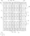
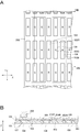
- FIG. 1A is a plan view showing a schematic configuration of an embodiment of a display device.
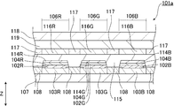
- FIG. 1B is a cross-sectional view showing a schematic configuration of a state of the IB-IB line cross section of FIG. 1A.
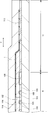
- FIG. 2 is a cross-sectional view showing a schematic configuration of a state of the cross-sectional view taken along line II-II of FIG. 1A.
- FIG. 3 is a diagram showing an embodiment of an energized state at the second electrode of the display device.
- FIG. 4 is a cross-sectional view showing a schematic configuration of an embodiment of an auxiliary electrode in a display device.
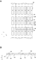
- FIG. 5A is a plan view showing an embodiment of a method for manufacturing a display device.
- FIG. 5A is a plan view showing an embodiment of a method for manufacturing a display device.
- FIG. 5B is a cross-sectional view showing a schematic configuration of a state of the VB-VB line cross section of FIG. 5A.
- FIG. 6A is a plan view showing an embodiment of a method for manufacturing a display device.
- FIG. 6B is a cross-sectional view showing a schematic configuration of a state of the VIB-VIB line cross section of FIG. 6A.
- FIG. 7A is a plan view showing an embodiment of a method for manufacturing a display device.
- FIG. 7B is a cross-sectional view showing a schematic configuration of a state of the VIIB-VIIB line cross section of FIG. 7A.
- FIG. 8A is a plan view showing an embodiment of a method for manufacturing a display device.
- FIG. 8A is a plan view showing an embodiment of a method for manufacturing a display device.
- FIG. 8B is a cross-sectional view showing a schematic configuration of a state of the VIIIB-VIIIB line cross section of FIG. 8A.
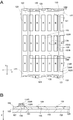
- FIG. 9A is a plan view showing a schematic configuration of a modified example of the display device.
- FIG. 9B is a cross-sectional view showing a schematic configuration of a state of the IXB-IXB line cross section of FIG. 9A.
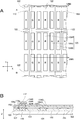
- FIG. 10A is a plan view showing a schematic configuration of a modified example of the display device.
- FIG. 10B is a cross-sectional view showing a schematic configuration of a state of the XB-XB line cross section of FIG. 10A.
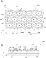
- FIG. 11A is a plan view showing a schematic configuration of a modified example of the display device.
- FIG. 11A is a plan view showing a schematic configuration of a modified example of the display device.
- FIG. 11B is a cross-sectional view showing a schematic configuration of a state of the XIB-XIB line cross section of FIG. 11A.
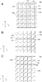
- 12A and 12B are plan views showing an embodiment of the second electrode.
- 13A, 13B, and 13C are plan views showing an embodiment of the second electrode.
- FIG. 14 is a diagram showing an embodiment of an energized state in the second electrode of the conventional display device.
- the display device 101a As shown in FIGS. 1A, 1B, 2 and the like, the display device 101a according to one of the embodiments of the present disclosure includes an organic compound layer 102 having a light emitting layer (102R, 102G in FIGS. 1B, 2 and the like). 102B) is provided.
- the first electrode 103 (103R, 103G, 103B in FIGS. 1B, 2 and the like) and the second electrode 104 (104R, 104G, 104B in FIGS. 1B, 2 and the like) are laminated with the organic compound layer 102 interposed therebetween. There is.
- the stacking direction of the first electrode 103, the organic compound layer 102, and the second electrode 104 in the display device 101a is the vertical direction (Z direction in FIGS. 1B and 2).
- the direction from the first electrode 103 to the second electrode 104 on the display device 101a is the upward direction, and the direction opposite to the upward direction is the downward direction.
- FIGS. 1A and 1B for convenience of explanation, the description of the layer and the member formed on the protective layer 114, which will be described later, is omitted. This also applies to the drawings of FIGS. 3 to 11 and 14.
- the relative magnitude ratios of the sizes and thicknesses of all the layers shown in FIGS. 1A, 1B, and 2 are described for convenience and do not specify the actual magnitude ratios.
- the definition and the magnitude ratio regarding the vertical direction are the same for each of the figures from FIGS. 3 to 14.
- a pixel area R and a non-pixel area U deviating from the pixel area R are formed, and pixels 105 are formed in the pixel area R in a pattern arranged in a two-dimensional manner.
- Each pixel 105 is composed of one type or a plurality of types of sub-pixels 106. Therefore, the sub-pixel 106 is formed in the pixel region R.
- the sub-pixels 106 are formed in an arrangement pattern that is separated from each other.
- the sub-pixel 106 has a laminated structure of the first electrode 103, the organic compound layer 102, and the second electrode 104.
- the sub-pixels 106 shown in the example of FIG. 1A and the like are formed in a two-dimensionally spaced arrangement pattern. In the present specification, the two-dimensional shape indicates the spread in the plane direction when a predetermined plane is assumed.
- Type of sub-pixel Examples of the criteria for determining the type of the sub-pixel 106 include differences in emission color, thickness of the organic compound layer 102, structure of the organic compound layer 102, and combinations thereof.
- the type of the sub-pixel 106 is based on the difference in emission color, for example, the sub-pixel 106 has a red sub-pixel 106R, a green sub-pixel 106G, and blue as the sub-pixel 106 having a different emission color as described above.
- the case where there are three types of sub-pixels 106B can be mentioned.
- the display device 101a uses red as the emission color (referred to as the red sub-pixel 106R) and green as the emission color as the sub-pixel 106.
- the description will be made by taking as an example the case of having three types of sub-pixels (referred to as green sub-pixel 106G) and sub-pixels having blue as the emission color (referred to as blue sub-pixel 106B).
- the unit of one pixel 105 is composed of a combination of these three types of sub-pixels 106R, 106G, and 106B.
- the color combination of the sub-pixels 106 constituting the pixel 105 is limited to the combination of three colors of red, green, and blue.
- the portions marked with the letters R, G, and B indicate the portions corresponding to the sub-pixel 106R, the sub-pixel 106G, and the sub-pixel 106B, respectively.
- the sub-pixel 106R, the sub-pixel 106G, and the sub-pixel 106B may be collectively referred to as the sub-pixel 106 when the type such as the color type is not particularly distinguished.
- the arrangement pattern of the sub-pixels 106 of each type is striped and arranged at positions deviated from each other. That is, with respect to the red sub-pixel 106R, one section of the sub-pixel 106R (hereinafter referred to as a unit section) is formed in an elongated rectangular shape, and is formed in the longitudinal direction (Y direction in the figure) and the longitudinal direction of the unit section.
- the unit compartments of the sub-pixel 106R are arranged two-dimensionally in the direction orthogonal to the direction (X direction in the figure). This also applies to the green sub-pixel 106G and the blue sub-pixel 106B.
- the red sub-pixel 106R, the green sub-pixel 106G, and the blue sub-pixel 106B are formed at positions deviated from each other in the X direction.
- the first electrode 103 is formed on the substrate 107.
- the first electrode 103 is patterned so as to correspond to the arrangement pattern of the sub-pixel 106, and is formed in a two-dimensionally spaced arrangement pattern for each unit section of the sub-pixel 106. ing.
- the first electrode 103R for red, the first electrode 103G for green, and the first electrode 103B for blue correspond to the three types of sub-pixels 106R, 106G, and 106B. Three types are formed.
- the first electrode 103R, the first electrode 103G, and the first electrode 103B may be collectively referred to as the first electrode 103 when the types such as color types are not particularly distinguished.
- a circuit such as a drive transistor for driving the display device 101a is formed on the substrate 107 (not shown).
- the circuit is electrically connected to the first electrode 103, and the energization state of the first electrode 103 is controlled.
- An insulating layer 108 having an opening 109 is formed between the adjacent first electrodes 103.
- the opening 109 of the insulating layer 108 is formed at the position where the first electrode 103 is formed in the plan view of the display device 101a.
- the opening 109 is formed in a pattern corresponding to the arrangement pattern of the sub-pixel 106, and one section of the opening 109 defines a unit section of the sub-pixel 106.
- the opening 109 may be formed so as to match the shape of the first electrode 103, or may be formed on the first electrode 103 as shown in the example of FIG. 1B.
- the insulating layer 108 covers the side end surface of the first electrode 103 and the outer edge portion on the upper surface side, and is formed so as to ride on the upper surface side of the first electrode 103. Will be done.
- the plan view of the display device 101a means a case where the vertical direction is the line-of-sight direction.
- the first electrode 103 functions as an electrode that controls the light emission of the sub-pixel 106 in combination with the second electrode 104 described later.
- the second electrode 104 becomes a cathode electrode
- the second electrode 104 becomes an anode electrode
- the first electrode 103 is made of a metal having a high work function, such as platinum, gold, silver, chromium, tungsten, nickel, copper, iron, cobalt, and tantalum. Is preferable.
- the first electrode 103 may be formed of the above-mentioned metal alloy having a high work function, and may be formed of, for example, an Ag—Pb—Cu alloy or an Al—Nd alloy.
- the first electrode 103 is made of a metal having a small work function.
- the first electrode 103 may be formed of a metal having a small work function and a conductive material having a high light reflectance, such as aluminum or an alloy containing aluminum.
- the first electrode 103 can be used as the anode electrode by providing the hole injection layer in the laminated structure forming the sub-pixel 106 to improve the hole injection property.
- the first electrode 103 includes indium oxide, indium-tin oxide (ITO: Indium Tin Oxide, Sn-doped indium oxide, crystalline ITO and amorphous ITO), indium-zinc oxide (IZO: Indium Zinc Oxide), and the like.
- ITO Indium Tin Oxide
- Sn-doped indium oxide crystalline ITO and amorphous ITO
- IZO Indium Zinc Oxide
- indium - gallium oxide IGO
- gallium indium doped - zinc oxide IGZO
- IFO F-doped in 2 O 3
- ITiO Ti -doped in 2 O 3
- InSnZnO tin oxide
- SnO 2 ATO
- Sb-doped SnO 2 FTO
- ZnO zinc oxide
- aluminum oxide-doped zinc oxide AZO
- B-doped ZnO AlMgZnO (aluminum oxide and zinc oxide doped with magnesium oxide
- antimony oxide titanium oxide, NiO, spinel-type oxides, and oxides having a YbFe 2 O 4 structure may be formed.
- the first electrode 103 is made of indium and tin on a multilayer film having gallium oxide, titanium oxide, niobium oxide, nickel oxide or the like as a base layer, or a reflective film having high light reflectivity such as aluminum. It may be formed in a structure in which transparent conductive materials having excellent hole injection characteristics such as oxide (ITO) and oxide of indium and zinc (IZO) are laminated.
- ITO oxide
- IZO indium and zinc
- An organic compound layer 102 is formed on the first electrode 103 and the insulating layer 108.
- the organic compound layer 102 includes at least a light emitting layer.
- the organic compound layer 102 is also formed on a part of the insulating layer 108.
- the light emitting layer is formed of an organic light emitting material.
- the electrons injected from each of the first electrode 103 and the second electrode 104 are combined with holes to generate light.
- the organic compound layer 102 having a light emitting layer using an organic light emitting material having a light emitting color corresponding to the type of the sub-pixel 106 is formed.
- an organic compound layer 102 corresponding to the type of sub-pixels 106 is formed in a pattern for each type of sub-pixels 106.
- the organic compound layer 102 for each emission color is provided. It is formed.
- 106B an organic compound layer 102B that emits blue light (wavelength: 450 nm to 495 nm) is formed.
- the organic compound layer 102R, the organic compound layer 102G, and the organic compound layer 102B are also collectively referred to as the organic compound layer 102.
- the organic compound layer 102R, the organic compound layer 102G, and the organic compound layer 102B are drawn so that the end faces of the portions extending in the Y direction are in contact with each other.
- the end faces of the organic compound layer 102R, the organic compound layer 102G, and the organic compound layer 102B are separated from each other. This also applies to the second electrode 104 and the protective layer 114.
- the organic compound layer 102 is formed on the first electrode 103 in a shape defined so as to close the opening 109 in the plan view of the display device 101a, and further, a pattern is formed in substantially the same shape as the second electrode 104. Will be done.
- the organic compound layer 102 is patterned in substantially the same shape as the second electrode 104, the second electrode 104R, the second electrode 104G, and the second electrode 104B are in direct contact with each other in and around the grade separation portion 112 described later. It becomes easy to avoid.
- the case where a plurality of objects are formed in substantially the same shape includes the case where they are formed in the same shape.
- the organic compound layer 102 When the organic compound layer 102 is formed in substantially the same shape as the second electrode 104, the organic compound layer 102 is patterned in a shape connected to each other between the sub-pixels 106. Further, the organic compound layer 102 has a branch. The branching position of the organic compound layer 102 is located immediately below the branching portion 122 of the second electrode 104. In the examples of FIGS. 1A, 1B, and 2, the organic compound layer 102 is connected to each other between the sub-pixels 106 across the sub-pixels 106 in the plan view of the display device 101a, that is, the organic compound layer 102 is subordinate. A plurality of rows extending in the Y direction are formed across adjacent unit sections of the pixels 106.
- the adjacent rows of the organic compound layer 102 are connected by a crosslinked portion extending in the X direction. Then, in the organic compound layer 102, a branch is formed at the connecting portion between the row portion and the crosslinked portion. This branch is arranged two-dimensionally like the second electrode 104.
- the organic compound layer 102 is formed in substantially the same shape as the second electrode 104, the steps of forming the pattern of the organic compound layer 102 and the second electrode 104 can be merged, and the treatment used at the time of pattern formation. It is possible to suppress the possibility that the liquid or the like affects the performance of the organic compound layer 102.
- the organic compound layer 102R, the organic compound layer 102G, and the organic compound layer 102B have substantially the same shape as the second electrode 104R, the second electrode 104G, and the second electrode 104B, respectively.
- the pattern is formed.
- the organic compound layer 102 is directed from the first electrode 103 toward the second electrode 104 (from bottom to top). It may have a structure in which a hole transport layer, a light emitting layer, and an electron transport layer are laminated in this order. When the organic compound layer 102 has such a structure, the luminous efficiency can be further increased. Further, the organic compound layer 102 has a structure in which a hole injection layer, a hole transport layer, a light emitting layer, an electron transport layer, and an electron injection layer are laminated in this order from the first electrode 103 to the second electrode 104. May be.
- the hole transport layer is a layer that enhances the hole transport efficiency to the light emitting layer.
- the hole injection layer is a layer that enhances the hole injection efficiency from the first electrode 103 to the hole transport layer.
- the electron injection layer is a layer that enhances the electron injection efficiency from the second electrode 104 to the electron transport layer.
- the electron transport layer is a layer that enhances the electron transport efficiency to the light emitting layer.
- the thicknesses of the organic compound layers 102 constituting the sub-pixels 106 may be different from each other. Therefore, the thickness of the organic compound layer 102 constituting each sub-pixel 106 may be set to an appropriate thickness according to the emission color. For example, different thicknesses may be set as the thicknesses of the organic compound layer 102R, the organic compound layer 102G, and the organic compound layer 102B.
- the end surface 102a of the organic compound layer 102 and the end surface 104a of the second electrode 104 form a continuous surface. It is preferably formed. In this case, as shown in the example of FIG. 1B, it is more preferable that the organic compound layer 102 and the second electrode 104 are formed in a tapered shape.
- the second electrode 104 is formed on the organic compound layer 102. As described above, the second electrode 104 functions as an electrode that controls the light emitting state of the sub-pixel 106 in combination with the first electrode 103.
- the second electrode 104 is formed according to the type of the sub-pixel 106. That is, when two or more types of sub-pixels 106 are provided, the second electrode 104 corresponding to each of the plurality of types of sub-pixels 106 is formed. In the examples of FIGS. 1A, 1B, and 2, the second electrode 104R for red, the second electrode 104G for green, and the second electrode for blue correspond to the sub-pixel 106R, the sub-pixel 106G, and the sub-pixel 106B, respectively. Three types of electrodes 104B are formed. In the present specification, the second electrode 104R, the second electrode 104G, and the second electrode 104B may be collectively referred to as the second electrode 104 when the type such as the color type is not particularly distinguished. ..
- the second electrode 104 straddles the sub-pixel 106 and is formed in a pattern in which the sub-pixels 106 are connected to each other. Further, the second electrode 104 has a plurality of branch portions 122 connected to each other. The branching portions 122 are arranged in a two-dimensional manner, and electrically connect the portions corresponding to the unit compartments of the sub-pixels 106 in the second electrode 104 to each other. In the example of FIG. 1A, the second electrode 104 has a row portion 120 continuous in the Y direction across adjacent unit compartments of the sub-pixel 106. As shown in FIG. 12A, the adjacent row portions 120 in the second electrode 104 are connected by a cross-linking portion 121 extending in the X direction.
- the branch portion 122 is formed at the connecting portion between the row portion 120 and the bridge portion 121, and the portion of the second electrode 104 that forms the branch portion 122 is two-dimensional in the X direction and the Y direction. They are arranged in a shape (in the example of FIGS. 1A and 12A, a grid shape). Note that FIG. 12A shows an example of the second electrode 104 of the display device 101a.
- the second electrode 104 is patterned so as to have a mesh shape. Since the second electrode 104 is formed in a mesh-like pattern, it becomes easy to realize a more uniform image display.
- the second electrode 104 is formed in a pattern that is connected in the X direction and the Y direction and spreads out in a grid pattern as a whole.
- each of the second electrode 104R, the second electrode 104G, and the second electrode 104B is formed in a pattern in which they are connected in a grid pattern in the X direction and the Y direction, respectively, and are connected to the whole.
- the grade separation portion 112 is formed at the portion where the second electrode 104R and the second electrode 104G intersect in the plan view of the display device 101a. Further, a grade separation portion 112 in which the second electrode 104R and the second electrode 104G intersect is formed.
- a grade separation portion 112 is formed at a portion where the second electrode 104G and the second electrode 104B intersect in the same manner.
- the upper and lower positions and the intersecting directions of the intersecting second electrode 104 are not particularly limited.
- the second electrode 104R and the second electrode 104G intersect either of them may be on the upper side.
- the number of intersecting second electrodes 104 is preferably up to two.
- the grade separation portion 112 is formed at a position avoiding the opening 109 of the insulating layer 108 in the plan view of the display device 101a. Since the grade separation portion 112 is formed at a position avoiding the opening 109, the possibility that the light emitting state of the sub-pixel 106 is affected by the grade separation portion 112 can be more reliably suppressed.
- the second electrode 104R is patterned so as to straddle between adjacent openings 109 with respect to the openings 109 forming the sub-pixel 106G. Further, the second electrode 104R is patterned so as to straddle between adjacent openings 109 about the openings 109 forming the sub-pixel 106B.
- the second electrode 104G straddles between adjacent openings 109 for each of the sub-pixel 106R and the sub-pixel 106B. Similar to the second electrode 104R, the second electrode 104B straddles between adjacent openings 109 for each of the sub-pixel 106R and the sub-pixel 106G.
- the second electrode 104 extends from the pixel region R to the non-pixel region U.
- the connection portion between the second electrode 104 and the external circuit can be positioned in the non-pixel region U.
- the description of the grade separation portion 112 is omitted in FIG.
- the auxiliary electrode portion 113 is formed in the non-pixel region U.
- the auxiliary electrode portion 113 is formed in a shape that surrounds the entire circumference or a part of the periphery of the pixel region R.
- the auxiliary electrode portion 113 may have, for example, a ring shape, a U shape, or the like in a plan view of the display device 101a.
- the auxiliary electrode portion 113 can be formed of the same material as the first electrode 103.
- the second electrode 104 is connected to the auxiliary electrode portion 113 formed in the non-pixel region U, as shown in FIG.
- the second electrode 104 can be electrically connected to the external circuit via the auxiliary electrode portion 113, and a path of the current i is formed from the first electrode through the second electrode toward the auxiliary electrode 13. be able to.
- the second electrode 104 may be formed of a metal oxide.
- a transparent conductive material such as IZO, ITO, ZnO, SnO, AZO, or GZO may be used.
- the second electrode 104 includes, for example, aluminum (Al), silver (Ag), magnesium (Mg), calcium (Ca), sodium (Na), strontium (Sr), alkali metal or alkaline earth metal and silver. It may be formed of an alloy of magnesium and silver, an alloy of magnesium and calcium, an alloy of aluminum and lithium (Li), or the like.
- a protective layer 114 is formed on the second electrode 104.
- the protective layer 114 is made of an insulating material.
- the insulating material for example, a thermosetting resin or the like can be used.
- SiN, SiO, SiON, AlO, TiO and the like may be used, or they may be laminated.
- the protective layer 114 a CVD film containing SiN, SiO, SION, etc., an ALD film containing AlO, TiO, SiO, etc., and the like can be exemplified.
- a protective layer 114 for each sub-pixel 106 is formed according to the type of the sub-pixels 106.
- the protective layer 114R, the protective layer 114G, and the protective layer 114B have patterns for each of the three types of sub-pixel 106R, sub-pixel 106G, and sub-pixel 106B, respectively. It is formed.
- the protective layer 114R, the protective layer 114G, and the protective layer 114B are not distinguished from each other, they are also collectively referred to as the protective layer 114.
- the protective layer 114 is patterned in substantially the same shape as the second electrode 104 in the plan view of the display device 101a.
- the protective layer 114 is formed to have substantially the same shape as the second electrode 104, the protective layer 114 is formed in a shape that straddles the sub-pixels 106 and is connected to each other between the sub-pixels 106. Further, the protective layer 114 has a branch. The branch position of the protective layer 114 is located immediately above the branch portion 122 of the second electrode 104. In the examples of FIGS.
- the protective layer 114 is connected to each other between the sub-pixels 106 across the sub-pixels 106 in the plan view of the display device 101a, that is, the protective layer 114 is the sub-pixels.
- a plurality of rows extending in the Y direction are formed across 106 adjacent unit sections.
- the adjacent rows of the protective layer 114 are connected by a cross-linked portion extending in the X direction.
- a branch is formed at the connecting portion between the row portion and the cross-linked portion. This branch is arranged two-dimensionally like the second electrode 104.
- the protective layer 114 is formed in substantially the same shape as the second electrode 104, but also the protective layer 114 and the organic compound layer 102 are formed in substantially the same shape.
- the steps of forming the pattern of the protective layer 114, the second electrode 104, and the organic compound layer 102 can be merged, and the treatment liquid used at the time of pattern formation may affect the performance of the organic compound layer 102. Can be suppressed.
- the protective layer 114R, the second electrode 104R, and the organic compound layer 102R are patterned in substantially the same shape.
- the protective layer 114G, the second electrode 104G, and the organic compound layer 102G are patterned in substantially the same shape as each other.
- the protective layer 114B, the second electrode 104B, and the organic compound layer 102B are patterned in substantially the same shape as each other.
- the end face 114a of the protective layer 114 and the organic compound layer 102 It is preferable that the end surface 102a of the second electrode 104 and the end surface 104a of the second electrode 104 form a continuous surface. Further, when the continuous surface is formed, it is preferable that the protective layer 114, the second electrode 104, and the organic compound layer 102 are formed in a tapered shape.
- the second electrode 104 located on the upper side of the grade separation 112 is the second electrode 104. It is possible to suppress the possibility of loss in and near the grade separation portion 112. Further, since the protective layer 114, the second electrode 104, and the organic compound layer 102 are formed in a tapered shape, it is possible to more effectively suppress defects in the grade separation portion 112 and its vicinity.
- the protective layer 114 covers the uppermost surface of the laminated structure of the organic compound layer 102 and the second electrode 104. By forming the protective layer 114, it is possible to regulate that the upper surface side of the laminated structure of the organic compound layer 102 and the second electrode 104 comes into mutual contact at the grade separation portion 112. In the example of FIG. 1B, for example, the laminated structure of the organic compound layer 102G and the second electrode 104G and the laminated structure of the organic compound layer 102B and the second electrode 104B are in contact with each other on the upper surface of the laminated structure of the organic compound layer 102R and the second electrode 104R. Is avoided.
- the filling layer 115 is formed on the protective layer 114.
- the filling layer 115 is formed so as to cover all of the protective layer 114G, the protective layer 114B, and the protective layer 114R.
- the packing layer 115 may be, for example, a layer formed of the same resin as the protective layer 114, a layer formed of an organic resin, or a laminate thereof.
- a laminated body a laminated body of a layer formed of the same resin as the protective layer 114 (referred to as a barrier layer) and a layer formed of an adhesive resin on the barrier layer is used. It can be exemplified.
- a resin or the like that forms a layer for the purpose of flattening can be exemplified, and specifically, a known material such as a thermosetting resin or an ultraviolet curable resin can be exemplified. ..
- a color filter 116 is arranged on the upper part of the packing layer 115 at a position corresponding to the sub-pixel 106.
- color filters 116 for each of the sub-pixels 106 are arranged according to the types of the sub-pixels 106.
- the red color filter 116R is arranged at the position corresponding to the sub-pixel 106R
- the green color filter 116G is arranged at the position corresponding to the sub-pixel 106G
- a blue color filter 116B is arranged at a position corresponding to the pixel 106B.
- the red color filter 116R, the green color filter 116G, and the blue color filter 116B may be collectively referred to as the color filter 116 when they are not distinguished from each other.
- the red color filter 116R, the green color filter 116G, and the blue color filter 116B adjust the color or wavelength of the light emitted from the organic compound layer 102R, the organic compound layer 102G, and the organic compound layer 102B, respectively.
- the red color filter 116R, the green color filter 116G, and the blue color filter 116B may not be provided in some cases.
- Black matrix A black matrix layer 117 is formed between adjacent color filters 116.
- the black matrix layer 117 can prevent the light emitted from the organic compound layer 102 from entering the color filter 116 of the other adjacent sub-pixels 106 and causing color mixing.
- the black matrix layer 117 may be, for example, a black resin film having an optical density of 1 or more mixed with a black colorant. Specifically, as a material of the black matrix layer 117, a black polyimide resin or the like can be exemplified. The black matrix layer 117 may not be provided.
- a lens (not shown) or the like is arranged above the layer on which the color filter 116 and the black matrix layer 117 are formed, and a sealing layer 119 or the like is further formed, and the facing glass is placed on the sealing layer 119. 118 is formed.
- the sealing layer 119 can be formed by using a resin or the like. By providing the sealing layer 119, it is possible to effectively prevent moisture or the like from entering the organic compound layer 102 from the outside.
- the sealing layer 115 for example, a layer made of an organic resin or the like may be adopted, and known materials such as a thermosetting resin and an ultraviolet curable resin can be exemplified.
- the opposing glass 118 may be formed of a substance that transmits light emitted from the organic compound layer 102.
- Examples of the facing glass 118 include various glass substrates such as high-strain point glass, soda glass, borosilicate glass, and lead glass, and quartz substrates.
- the lens may be provided under the layer on which the color filter 116 is formed.
- FIG. 3 shows an example of the state of the second electrode 104 when the second electrode 104 of the display device 101a is defective.
- FIG. 14 shows an example of the state of the second electrode S when the second electrode S of the conventional display device is defective. Further, in FIG. 3, arrows Yi and Xi indicate directions in which a current can flow in the second electrode 104 of the display device 101a. In FIG. 14, the arrow Yic indicates a direction in which a current can flow in the second electrode S.
- the current can flow not only in the Y direction but also in the X direction, so that the path through which the current flows in the second electrode 104 increases. Therefore, the influence of the variation in the wiring resistance can be suppressed, and for example, the variation in the brightness of the display device 101a can be suppressed. This can be realized more effectively when the second electrode 104 is formed in a mesh pattern.
- a resist matching the pattern shape of the second electrode 104 is provided as a resist for forming a pattern of the organic compound layer 102, the second electrode 104, and the protective layer 114.
- the resist also has a mesh shape, so that the resist does not easily collapse even if a high-definition pattern is formed, and a defect occurs at the time of pattern formation. The possibility can be suppressed.
- the first electrode 103 is formed on the substrate 107 including the drive circuit such as the drive transistor for driving the display device 101a, and the insulating layer 108 is further laminated.
- An opening 109 is formed in the insulating layer 108 according to the pattern of the sub-pixel 106.
- a sputtering method, a CVD (Chemical Vapor Deposition), or an ALD (Atomic Layer Deposition) method can be used.
- a metal layer made of ITO is formed as a first electrode 103 on a substrate 107 in which a circuit layer including a drive circuit is formed on a Si substrate, and a metal layer is formed using photolithography technology and etching technology. Patterning.
- the first electrode 103 is formed in a two-dimensionally spaced arrangement pattern for each unit section of one sub-pixel 106.
- the first electrode 103 (103R, 103G, 103B) is formed at a position corresponding to the three types of sub-pixels 106 (106R, 106G, 106B).
- the insulating layer 108 is formed on the forming surface of the first electrode 103 on the substrate 107, and the opening 109 is formed in a pattern according to the pattern of the sub-pixel 106. At this time, the insulating layer 108 is formed so as to fill the region between the opening 109 and the patterned metal layer.
- the insulating layer 108 may be formed of SiON or the like.
- Step of forming a laminated structure of the protective layer 114R, the second electrode 104R and the organic compound layer 102R On the first electrode 103 and the insulating layer 108, as shown in FIGS. 6A and 6B, a layer 202R forming the organic compound layer 102R corresponding to the sub-pixel 106R, a layer 204R forming the second electrode 104R, and protection.
- the layer 214R forming the layer 114R is formed in this order.
- Examples of the method for forming each of these layers include a vacuum deposition method, sputtering, CVD (chemical vapor deposition), ALD (Atomic Layer Deposition), and the like, and further, a coating method such as a spin coating method and a die coating method can be used. Can be mentioned.
- the configuration of the layer 202R forming the organic compound layer 102R is determined according to the layer configuration of the organic compound layer 102R in the display device 101a.
- the layer 202R forming the organic compound layer 102R is an electron transport layer and a light emitting layer. It may be a stack of layers forming each of the hole transport layer and the hole transport layer.
- the second electrode 104R is composed of IZO
- an IZO film may be formed as the layer 204R forming the second electrode 104R.
- a CVD film containing SiN, SiO, SION and the like can be mentioned.
- the resist 200 is formed on the layer 214R forming the protective layer 114R.
- the resist 200 is patterned so as to correspond to the shape of the second electrode 104R.
- a resist 200 is formed on the surface of the laminate with respect to the laminate in which the layer 202R forming the organic compound layer 102R, the layer 204R forming the second electrode 104R, and the layer 214R forming the protective layer 114R are laminated, and the resist 200 is formed.
- a photolithography method, a dry etching method, or the like is applied using the mask.
- a laminated structure of the protective layer 114R, the second electrode 104R, and the organic compound layer 102R is formed on the first electrode 103R.
- the protective layer 114R and the organic compound layer 102R are formed to have substantially the same shape as that of the second electrode 104R.
- the resist 200 formed on the protective layer 114R is removed.
- a method using ashing, a removing liquid, or the like can be used.
- Step of forming a laminated structure of the protective layer 114G, the second electrode 104G and the organic compound layer 102G uses the same method as the step of forming the laminated structure of the protective layer 114R, the second electrode 104R and the organic compound layer 102R. Will be implemented. Instead of the resist 200 corresponding to the shape of the second electrode 104R, a resist corresponding to the shape of the second electrode 104G is used. As a result, as shown in FIGS. 8A and 8B, a laminated structure of the protective layer 114G, the second electrode 104G, and the organic compound layer 102G is formed. In FIG. 8A, the description of the protective layer 114R and the organic compound layer 102R and the protective layer 114G and the organic compound layer 102G are omitted for convenience of explanation.
- Step of forming a laminated structure of the protective layer 114B, the second electrode 104B and the organic compound layer 102B After the laminated structure of the protective layer 114G, the second electrode 104G and the organic compound layer 102G is formed, the step of forming the laminated structure of the protective layer 114B, the second electrode 104B and the organic compound layer 102B is performed on the protective layer 114R and the second electrode. It is carried out by using the same method as the step of forming the laminated structure of 104R and the organic compound layer 102R. Instead of the resist 200 corresponding to the shape of the second electrode 104R, a resist corresponding to the shape of the second electrode 104B is used. As a result, as shown in FIGS.
- the laminated structure of the protective layer 114R, the second electrode 104R and the organic compound layer 102R, and the laminated structure of the protective layer 114G, the second electrode 104G and the organic compound layer 102G are protected.
- a laminated structure of the layer 114B, the second electrode 104B, and the organic compound layer 102B is formed.
- the order in which the steps of forming the laminated structure of the organic compound layer 102B are carried out is not limited to the above order.
- the packing layer 115 is formed so as to cover all of the protective layer 114R, the protective layer 114G, and the protective layer 114B.
- the packed layer 115 can be obtained by forming a layer made of the same resin as the protective layer 114 on one surface, and further forming a layer made of an adhesive resin or the like on the layer.
- the arrangement surface side of the color filter 116 is made to face the filling layer 115 side.
- the laminated parts are fixed on the packed layer 115. In this way, the display device 101a is formed.
- the black matrix layer 117 and the sealing layer 119 may be omitted.
- each layer such as the color filter 116 and the black matrix layer 117 may be sequentially formed on the packed layer 115.
- the filling layer 115 formed in the packing layer forming step does not have to have a layer formed of an adhesive resin or the like.
- the filling layer 115 a layer formed of the same resin as the protective layer 114, a layer formed of an organic resin, or the like may be adopted.
- the organic resin as described above, a resin that forms a layer for the purpose of flattening can be exemplified.
- the color filter 116 and the black matrix layer 117 are formed on the filling layer 115.
- a lens is arranged on the color filter 116.
- a resin that forms the sealing layer 119 is applied to one surface so as to cover the surface on which the lens is arranged.
- the facing glass 118 is arranged on the resin surface coated on one surface, and the facing glass 118 is fixed by solidifying the sealing layer 119. In this way, the display device 101a is formed. Even in this case, the black matrix layer 117 may not be provided as described above.
- the resin forming the sealing layer 119 for example, an ultraviolet curable resin or a thermosetting resin can be used as the resin forming the sealing layer 119.
- Etc. are applied to form the protective layer 114, the second electrode 104, and the organic compound layer 102. Therefore, the end surface 102a of the organic compound layer 102, the end surface 104a of the second electrode 104, and the end surface 114a of the protective layer 114 can be continuous surfaces.
- the end surface 102a of the organic compound layer 102, the end surface 104a of the second electrode 104, and the end surface 114a of the protective layer 114 are continuous surfaces (facial), so that the grade separation portion 112 is formed during the manufacture of the display device 101a. It is possible to suppress the possibility of causing a defect in the second electrode 104 in and in the vicinity thereof.
- the end face 102a of the organic compound layer 102, the end face 104a of the second electrode 104, and the end face 114a of the protective layer 114 are continuous faces, and the organic compound layer 102 and the second electrode are further formed.
- the 104 and the protective layer 114 can be formed in a tapered shape.
- the organic compound layer 102, the second electrode 104, and the protective layer 114 are tapered, and the end faces 102a, 104a, 114a form a continuous surface as follows. It works. That is, at the time of manufacturing the display device 101a, it is possible to suppress the possibility that the second electrode 104 located on the upper side of the grade separation portion 112 causes a defect in the grade separation portion 112 and its vicinity.
- the organic compound layer 102G, the second electrode 104G, and the protective layer are formed.
- a state in which the laminated structure of 114G rides on the laminated structure of the organic compound layer 102R, the second electrode 104R, and the protective layer 114R is formed.
- the organic compound layer 102R, the second electrode 104R, and the protective layer 114R are tapered and the end faces 102a, 104a, 114a form a continuous surface, so that the organic compound layer 102R, the second electrode 104R, and the protective layer 114R are formed.
- the end face of the laminated structure is a smooth inclined surface. Therefore, the laminated structure of the organic compound layer 102G, the second electrode 104G, and the protective layer 114G can be smoothly mounted on the laminated structure of the organic compound layer 102R, the second electrode 104R, and the protective layer 114R, and the second electrode The possibility of causing a defect in 104G can be suppressed.
- the arrangement pattern of the sub-pixel 106 is not limited to this.
- the arrangement pattern of the sub-pixel 106 may be any of a matrix shape, a delta shape, and a combination of a stripe shape and a matrix shape.
- Modification example 1 In the display device 101b shown in the examples of FIGS. 9A and 9B, three types of sub-pixels 106 are used: a red sub-pixel 106R, a blue sub-pixel 106G, and a green sub-pixel 106B.
- the arrangement pattern is delta-shaped. That is, the shape obtained by connecting the combination of three sections (unit sections of the sub-pixel 106) for the sub-pixel 106R is an acute triangle (delta shape), and the combination of the three unit sections forming the acute triangle is They are arranged in two dimensions. The unit compartments are separated from each other.
- the sub-pixel 106G and the sub-pixel 106B and the three types of the sub-pixel 106R, the sub-pixel 106G, and the sub-pixel 106B are arranged so as to be alternately arranged at positions shifted in a predetermined direction (X direction in FIG. 9A). ing. Further, the three types of combinations of the sub-pixel 106R, the sub-pixel 106G, and the sub-pixel 106B arranged in the X direction are arranged side by side in the K1 direction diagonally crossing the X direction. Further, the three types of combinations of the sub-pixels 106 are arranged side by side in the K2 direction which crosses diagonally with respect to the X direction.
- the second electrode 104 is formed in a shape that straddles the sub-pixel 106 and is connected to each other between the sub-pixels 106. Further, as shown in FIG. 12B, the second electrode 104 has a plurality of branch portions 122 connected to each other. Further, the branch portion 122 is arranged two-dimensionally. As shown in FIG. 12B, the second electrode 104 forms continuous rows 120a and 120b in the K1 direction and the K2 direction across adjacent unit sections of the sub-pixel 106, and branches at the position of the sub-pixel 106. The portion 122 is formed. The organic compound layer 102 and the protective layer 114 are also patterned in the same shape as the second electrode 104. Note that FIG. 12B shows an embodiment of the second electrode 104 in the first modification.
- the shape of the unit section of the sub-pixel 106 is an elliptical shape in the example of FIG. 9A, but the shape of the unit section of the sub-pixel 106 is not limited to this, and the shape is not limited to this, such as a hexagon. It may be a polygon, a triangle, a rectangle, a perfect circle, or the like.
- Modification 2 In the display device 101c shown in the examples of FIGS. 10A and 10B, three types of sub-pixels 106 are used: a red sub-pixel 106R, a blue sub-pixel 106G, and a green sub-pixel 106B.
- the arrangement pattern is a matrix. That is, the unit compartments are arranged in a matrix for the sub-pixel 106R. The same applies to the sub-pixel 106G.
- the sub-pixels 106B are arranged in a matrix for each of the two diagonally arranged unit sections. In the unit section of the pixel 105, one unit section of the sub-pixel 106R, one unit section of the sub-pixel 106G, and two unit sections of the sub-pixel 106B arranged diagonally are arranged.
- the shape of the unit section of the sub-pixel 106 is square in the example of FIG. 10A, but the shape of the unit section of the sub-pixel 106 is not limited to this.
- the second electrode 104 is formed in a pattern that straddles the sub-pixels 106 and is connected to each other between the sub-pixels 106. Further, the second electrode 104 has a plurality of branch portions 122 connected to each other as shown in FIGS. 13A to 13C. In the second electrode 104, the branch portion 122 is arranged two-dimensionally. In the example of FIG. 10A, the second electrode 104 has row portions 120a and 120b extending in the Y direction and the X direction as shown in FIGS. 13A to 13C, and at the intersection position of the row portion 120a and the row portion 120b. A branch portion 122 is formed. FIG.
- FIG. 13A shows an embodiment of the second electrode 104 (104B) for the sub-pixel 106B
- FIG. 13B shows an embodiment of the second electrode 104 (104G) for the sub-pixel 106G
- FIG. 13C shows an embodiment of the second electrode 104 (104G).
- An embodiment of the second electrode 104 (104R) for the sub-pixel 106R is shown.
- the extension portion 123 extends two-dimensionally from the branch portion 122 of the second electrode 104 so as to straddle the sub-pixel 106.
- FIG. 13A a state in which two extending portions 123 are formed from one branch portion 122 is formed.
- FIGS. 13B and 13C one extension portion 123 is formed from one branch portion 122.
- the organic compound layer 102 and the protective layer 114 are also patterned in the same shape as the second electrode 104.
- Modification example 3 In the display device 101d shown in the examples of FIGS. 11A and 11B, three types of sub-pixels 106R, sub-pixels 106G, and sub-pixels 106B are used as sub-pixels 106, and the arrangement patterns of the sub-pixels 106 are striped and matrix. It is a combination of shapes. That is, unit sections are arranged in a matrix for the sub-pixel 106R and the sub-pixel 106G. The unit compartments of the sub-pixel 106B are arranged in a stripe shape.
- the second electrode 104 is formed in a shape that straddles the sub-pixels 106 and is connected to each other between the sub-pixels 106. Further, the second electrode 104 has a plurality of branch portions 122 connected to each other.
- the second electrode 104 can be formed as shown in FIGS. 13B and 13C, as in the second modification.
- the second electrode 104 (104B) can be formed in the same manner as in FIG. 12A.
- the organic compound layer 102 and the protective layer 114 are also patterned in the same shape as the second electrode 104.
- the same effect as that of the display device 101a can be sold for any of the display devices 101b, 101c, and 101d of the modified examples 1 to 3. For example, it is possible to avoid the occurrence of interruption of energization in the sub-pixel 106 when the second electrode 104 is defective, and it is possible to suppress the occurrence of line defects in the images displayed on the display devices 101b, 101c, 101d. Become.
- the present disclosure is not limited to the above-mentioned examples of the display device, the manufacturing method and the modified example, and the present disclosure is not limited to the above-mentioned examples.
- Various modifications based on technical ideas are possible.
- the configurations, methods, processes, shapes, materials, numerical values, etc. given in the above-mentioned display device, manufacturing method, and modification examples are merely examples, and if necessary, different configurations, methods, processes, and shapes are used. , Materials, numerical values, etc. may be used.
- the materials exemplified in the above-mentioned display device, manufacturing method, and modification can be used alone or in combination of two or more.
- the present disclosure may also adopt the following configuration.
- Sub-pixels having a structure in which a first electrode and a second electrode are laminated with an organic compound layer having a light emitting layer interposed therebetween are formed in an arrangement pattern having an arrangement two-dimensionally separated from each other.
- the second electrode has a pattern formed in a shape that straddles the sub-pixels and connects the sub-pixels to each other, has a plurality of branch portions connected to each other, and arranges the branch portions in a two-dimensional manner.
- the display device. (2) The display device according to (1) above, wherein the second electrode is formed in a mesh pattern. (3) It has a pixel area and a non-pixel area.
- the sub-pixel is formed in the pixel region,
- the second electrode extends from the pixel region to the non-pixel region.
- An auxiliary electrode portion is formed in the non-pixel region.
- the second electrode is connected to the auxiliary electrode portion.
- Two or more types of the sub-pixels are provided.
- the organic compound layer corresponding to the type of the sub-pixel is formed in a pattern.
- the type of the sub-pixel is based on the difference in emission color.
- Two or more types of the sub-pixels are provided.
- the second electrode is patterned according to the type of the sub-pixel.
- a grade separation portion is formed between a part of the second electrode forming the sub-pixel of a predetermined type and a part of the second electrode forming the sub-pixel of a type different from the predetermined type. ing, The display device according to (7) above. (9) An insulating layer having an opening formed in a pattern corresponding to the arrangement pattern of the sub-pixels is provided. The display device according to (8) above, wherein the grade separation portion is formed at a position avoiding the opening. (10) The first electrode is the anode electrode, The second electrode is the cathode electrode, The display device according to any one of (1) to (9) above.
- the arrangement pattern of the sub-pixels is selected from any of a group consisting of a stripe shape, a matrix shape, a delta shape, and a combination of the stripe shape and the matrix shape.
- (12) The end face of the second electrode and the end face of the organic compound layer form a continuous surface.
- Two or more types of the sub-pixels are provided.
Landscapes
- Physics & Mathematics (AREA)
- Engineering & Computer Science (AREA)
- Microelectronics & Electronic Packaging (AREA)
- Optics & Photonics (AREA)
- General Physics & Mathematics (AREA)
- Theoretical Computer Science (AREA)
- Electroluminescent Light Sources (AREA)
- Devices For Indicating Variable Information By Combining Individual Elements (AREA)
Abstract
表示装置において、発光層を有する有機化合物層を挟んで第1電極及び第2電極を積層した構造を有する副画素が、二次元状に互いに離間した配列を有する配置パターンで形成されており、前記第2電極は、前記副画素を跨ぎ前記副画素間で互いに繋がる形状にパターン形成されており、互いに接続される複数の分岐部を有し、且つ該分岐部を二次元状に配置している。
Description
本開示は、表示装置に関し、特に、第1電極と有機化合物層と第2電極とを積層した構造を有する表示装置に関する。
有機EL素子などの発光素子を用いた表示装置として、1つの画素を構成する副画素の単位で互いに離間した配置パターンで形成された第1電極の上に発光層を含む有機化合物層と第2電極とを積層した構造を有するものが知られている。有機化合物層や第2電極などの各層は、蒸着技術による方法、印刷技術による方法、エッチングによる方法、フォトリソグラフィを用いる方法などの形成方法を用いてパターン形成されている。
1つの画素を構成する1種または複数種類の副画素について、それぞれの種類の副画素の形成パターンに応じて有機化合物層と第2電極のパターンが定められている。有機化合物層と第2電極のパターンとしては、例えば、特許文献1の技術では、副画素を跨ぐストライプ状のパターンが形成されている。
特許文献1の技術には、配線の機能を兼ねている第2電極に欠損を生じた場合にあっても表示装置に表示される画像の線欠陥の発生を効果的に抑制する点で改善の余地がある。
本開示は、上述した点に鑑みてなされたものであり、第2電極に欠損を生じた場合にあっても表示装置に表示される画像の線欠陥の発生を抑制することの可能な表示装置の提供を目的の一つとする。
本開示は、例えば、発光層を有する有機化合物層を挟んで第1電極及び第2電極を積層した構造を有する副画素が、離間した配置パターンで形成されており、
前記第2電極は、前記副画素を跨ぎ前記副画素間で互いに繋がる形状にパターン形成されており、互いに接続される複数の分岐部を二次元状に配置している、表示装置である。
前記第2電極は、前記副画素を跨ぎ前記副画素間で互いに繋がる形状にパターン形成されており、互いに接続される複数の分岐部を二次元状に配置している、表示装置である。
以下、本開示にかかる一実施例等について図面を参照しながら説明する。なお、説明は以下の順序で行う。本明細書及び図面において、実質的に同一の機能構成を有する構成については、同一の符号を付することにより重複説明を省略する。
なお、説明は以下の順序で行うものとする。
1.表示装置
2.表示装置の製造方法
3.表示装置の変形例
1.表示装置
2.表示装置の製造方法
3.表示装置の変形例
以下の説明は本開示の好適な具体例であり、本開示の内容は、これらの実施の形態等に限定されるものではない。
[1.表示装置]
本開示の実施例の一つにかかる表示装置101aは、図1A、図1B、図2などに示すように、発光層を有する有機化合物層102(図1B、図2等では、102R、102G、102B)を備える。有機化合物層102を挟んで第1電極103(図1B、図2等では、103R、103G、103B)及び第2電極104(図1B、図2等では、104R、104G、104B)が積層されている。なお、説明の便宜上、表示装置101aにおける第1電極103と有機化合物層102と第2電極104の積層方向を上下方向(図1B、図2においてZ方向)とする。表示装置101aにおける第1電極103から第2電極104に向かう方向を上方向とし、その上方向に対する逆向きを下方向とする。また、図1A、図1Bでは、説明の便宜上、後述の保護層114上に形成される層や部材の記載を省略している。これは、図3から図11、図14の各図についても同様である。また、全ての図1A、図1B、図2に示す各層の大きさや厚みの相対的な大小比率は便宜上の記載であり、実際の大小比率を規定するものではない。これらの上下方向に関する定めや大小比率については、図3から図14までの各図についても同様である。
本開示の実施例の一つにかかる表示装置101aは、図1A、図1B、図2などに示すように、発光層を有する有機化合物層102(図1B、図2等では、102R、102G、102B)を備える。有機化合物層102を挟んで第1電極103(図1B、図2等では、103R、103G、103B)及び第2電極104(図1B、図2等では、104R、104G、104B)が積層されている。なお、説明の便宜上、表示装置101aにおける第1電極103と有機化合物層102と第2電極104の積層方向を上下方向(図1B、図2においてZ方向)とする。表示装置101aにおける第1電極103から第2電極104に向かう方向を上方向とし、その上方向に対する逆向きを下方向とする。また、図1A、図1Bでは、説明の便宜上、後述の保護層114上に形成される層や部材の記載を省略している。これは、図3から図11、図14の各図についても同様である。また、全ての図1A、図1B、図2に示す各層の大きさや厚みの相対的な大小比率は便宜上の記載であり、実際の大小比率を規定するものではない。これらの上下方向に関する定めや大小比率については、図3から図14までの各図についても同様である。
表示装置101aにおいては、画素領域Rと、画素領域Rから外れた非画素領域Uとが形成されており、画素領域Rに、二次元状に配列されたパターンで画素105が形成されている。それぞれの画素105は1種類または複数種類の副画素106で構成されている。したがって、画素領域Rに副画素106が形成される。副画素106は、互いに離間した配置パターンで形成される。副画素106は、第1電極103と有機化合物層102と第2電極104との積層構造を有する。図1A等の例に示す副画素106では、二次元状に互いに離間した配置パターンで形成されている。本明細書において、二次元状とは、所定の面を想定した場合に、その面方向の広がりを示す。
(副画素の種類)
副画素106の種類を定める基準としては、発光色、有機化合物層102の厚み、有機化合物層102の構造、それらの組合せ等の違い等を例示できる。副画素106の種類が発光色の違いを基準とする場合については、例えば、副画素106が、上記したように発光色の異なる副画素106として赤色の副画素106R、緑色の副画素106G、青色の副画素106Bの3種類である場合を挙げることができる。
副画素106の種類を定める基準としては、発光色、有機化合物層102の厚み、有機化合物層102の構造、それらの組合せ等の違い等を例示できる。副画素106の種類が発光色の違いを基準とする場合については、例えば、副画素106が、上記したように発光色の異なる副画素106として赤色の副画素106R、緑色の副画素106G、青色の副画素106Bの3種類である場合を挙げることができる。
以下では、図1A、図1B、図2に示すように、表示装置101aが、副画素106として、赤色を発光色とする副画素(赤色の副画素106Rと呼ぶ)、緑色を発光色とする副画素(緑色の副画素106Gと呼ぶ)、青色を発光色とする副画素(青色の副画素106Bと呼ぶ)の3種類を有する場合を例として説明が進められる。図1Aの例では、1つの画素105の単位は、これら3種類の副画素106R、106G、106Bの組合せで構成される。ただし、このことは、複数種類の副画素106で画素105が形成される場合に、画素105を構成する副画素106の色の組合せを赤、緑、青の3色の組み合わせに限定するものではない。なお、図1Aにおいて、R、G、Bの文字を付した部分は、それぞれ副画素106R、副画素106G、副画素106Bに対応する部分であることを示す。これは図3、図5から図13の各図においても同様である。なお、本明細書においては、副画素106R、副画素106G、副画素106Bについて、特に色種などの種類を区別しない場合には、まとめて副画素106と称することがある。
(副画素の配置パターン)
図1Aの例では、それぞれの種類の副画素106の配置パターンはストライプ状となっており、互いにずれた位置に配置されている。すなわち、赤色の副画素106Rについて、副画素106Rの1つの区画(以下、単位区画と呼ぶ)が細長い矩形状に形成されており、単位区画の長手方向(図においてY方向)とその長手方向に対して直交する方向(図においてX方向)に副画素106Rの単位区画が二次元状に並んでいる。このことは、緑色の副画素106G、青色の副画素106Bについても同様である。そして、赤色の副画素106R、緑色の副画素106G、青色の副画素106Bは、それぞれX方向に互いにずれた位置に形成される。
図1Aの例では、それぞれの種類の副画素106の配置パターンはストライプ状となっており、互いにずれた位置に配置されている。すなわち、赤色の副画素106Rについて、副画素106Rの1つの区画(以下、単位区画と呼ぶ)が細長い矩形状に形成されており、単位区画の長手方向(図においてY方向)とその長手方向に対して直交する方向(図においてX方向)に副画素106Rの単位区画が二次元状に並んでいる。このことは、緑色の副画素106G、青色の副画素106Bについても同様である。そして、赤色の副画素106R、緑色の副画素106G、青色の副画素106Bは、それぞれX方向に互いにずれた位置に形成される。
(第1電極)
表示装置101aにおいては、基板107の上に第1電極103が形成されている。
表示装置101aにおいては、基板107の上に第1電極103が形成されている。
第1電極103は、副画素106の配置パターンに対応するような配置となるようにパターン形成(パターニング)されており、副画素106の単位区画ごとに二次元状に離間した配置パターンで形成されている。図1A、図1B、図2の例では、3種類の副画素106R,106G,106Bに対応して、赤色用の第1電極103R、緑色用の第1電極103G、青色用の第1電極103Bの3種類が形成されている。なお、本明細書においては、第1電極103R、第1電極103G、第1電極103Bについて、特に色種などの種類を区別しない場合には、まとめて第1電極103と称することがある。
基板107には、表示装置101aを駆動させるための駆動トランジスタ等の回路が形成されている(図示せず)。回路は、第1電極103に電気的に接続されており、第1電極103への通電状態が制御される。
隣り合う第1電極103の間には、開口部109を有する絶縁層108が形成されている。絶縁層108の開口部109は、表示装置101aの平面視上、第1電極103の形成された位置に形成されている。開口部109は、副画素106の配置パターンに応じたパターンで形成されており、開口部109の1つの区画が副画素106の単位区画を定義する。なお、開口部109は、第1電極103の形状に整合するように形成されてもよいし、図1Bの例に示すように、第1電極103上に形成されてもよい。開口部109が第1電極103上に形成されている場合には、絶縁層108は第1電極103の側端面と上面側の外縁部を覆い、第1電極103の上面側に乗り上げるように形成される。なお、表示装置101aの平面視上とは、上下方向を視線方向とした場合を示すものとする。
第1電極103は、後述の第2電極104と組み合わせて副画素106の発光を制御する電極として機能する。第1電極103がアノード電極である場合、第2電極104がカソード電極となり、第1電極103がカソード電極である場合、第2電極104がアノード電極となる。
第1電極103がアノード電極である場合、第1電極103は、例えば、白金、金、銀、クロム、タングステン、ニッケル、銅、鉄、コバルト、タンタル等、仕事関数の高い金属で形成されることが好ましい。その他にも、第1電極103は、上述した仕事関数の高い金属の合金で形成されてもよく、例えば、Ag-Pb-Cu合金、Al-Nd合金で形成されてよい。
ただし、このことは、第1電極103が、仕事関数の小さい金属で形成されることを規制するものではない。例えば、第1電極103として、アルミニウム又はアルミニウムを含む合金等といった仕事関数の小さい金属且つ光反射率の高い導電材料で形成されてよい。この場合、副画素106を形成する積層構造内に正孔注入層を設けて正孔注入性を向上させることで、第1電極103をアノード電極として用いることができる。
第1電極103は、酸化インジウム、インジウム-錫酸化物(ITO:Indium Tin Oxide、Snドープの酸化インジウム、結晶性ITOおよびアモルファスITOを含む)、インジウム-亜鉛酸化物(IZO:Indium Zinc Oxide)、インジウム-ガリウム酸化物(IGO)、インジウム・ドープのガリウム-亜鉛酸化物(IGZO)、IFO(FドープのIn2O3)、ITiO(TiドープのIn2O3)、InSnZnO、酸化錫(SnO2)、ATO(SbドープのSnO2)、FTO(FドープのSnO2)、酸化亜鉛(ZnO)、酸化アルミニウム・ドープの酸化亜鉛(AZO)、ガリウム・ドープの酸化亜鉛(GZO)、BドープのZnO、AlMgZnO(酸化アルミニウムおよび酸化マグネシウム・ドープの酸化亜鉛)、酸化アンチモン、酸化チタン、NiO、スピネル型酸化物、YbFe2O4構造を有する酸化物で形成されてもよい。また、第1電極103は、ガリウム酸化物、チタン酸化物、ニオブ酸化物、若しくはニッケル酸化物等を母層とする多層膜、又はアルミニウムといった光反射性の高い反射膜の上にインジウムと錫の酸化物(ITO)、インジウムと亜鉛の酸化物(IZO)等の正孔注入特性に優れた透明導電材料を積層した構造にて形成されてもよい。
(有機化合物層)
第1電極103と絶縁層108の上には、有機化合物層102が形成されている。有機化合物層102は、少なくとも発光層を含む。有機化合物層102は、絶縁層108の一部上にも形成されている。
第1電極103と絶縁層108の上には、有機化合物層102が形成されている。有機化合物層102は、少なくとも発光層を含む。有機化合物層102は、絶縁層108の一部上にも形成されている。
発光層は有機発光材料で形成される。発光層では、第1電極103および第2電極104の各々から注入された電子と正孔との結合が生じ、光が発生する。表示装置101aでは、副画素106の種類に応じた発光色を有する有機発光材料を用いた発光層を有する有機化合物層102が形成される。副画素106が2種類以上設けられている場合、それぞれの種類の副画素106に対して、副画素106の種類に応じた有機化合物層102がパターン形成される。
図1A、図1B、図2の例に示す表示装置101aでは、発光色が異なる副画素106R、副画素106G、副画素106Bの3種類が設けられており、発光色ごとの有機化合物層102が形成される。副画素106Rに対しては、赤色(波長:620nm~750nm)を発光する有機化合物層102R、副画素106Gに対しては、緑色(波長:495nm~570nm)を発光する有機化合物層102G、副画素106Bに対しては、青色(波長:450nm~495nm)を発光する有機化合物層102Bが形成されている。有機化合物層102R、有機化合物層102G、有機化合物層102Bについて、これらの各々を区別しない場合には、まとめて有機化合物層102とも称する。なお、図1Aでは、説明の便宜上、有機化合物層102R、有機化合物層102G、有機化合物層102Bについて、Y方向に延びる部分の端面が互いに接しているように描かれているが、通常は、図2に示すように、有機化合物層102R、有機化合物層102G、有機化合物層102Bについて端面は離間している。このことは、第2電極104、保護層114についても同様である。
有機化合物層102は、表示装置101aの平面視上、開口部109を塞ぐように定められた形状で第1電極103上に形成されており、さらに、第2電極104とほぼ同形状にパターン形成される。有機化合物層102が第2電極104とほぼ同形状にパターン形成されていると、後述の立体交差部112及びその周囲での第2電極104R、第2電極104G、第2電極104B相互の直接接触を避けることが容易となる。本明細書において、複数の対象がほぼ同形状に形成されているという場合には、同形状に形成されている場合が含まれる。
有機化合物層102が第2電極104とほぼ同形状に形成される場合、有機化合物層102は、副画素106間で互いに繋がった形状にパターン形成されている。また、有機化合物層102は、分岐を有している。有機化合物層102の分岐位置は、第2電極104の分岐部122の直下側に位置する。図1A、図1B、図2の例では、有機化合物層102は、表示装置101aの平面視上、副画素106を跨いで副画素106間で互いに繋がっており、すなわち有機化合物層102は、副画素106の隣り合う単位区画を跨いでY方向に延びる複数の列部を形成している。有機化合物層102の隣り合う列部は、X方向に延びる架橋部で繋がっている。そして、有機化合物層102においては、列部と架橋部との接続部で分岐が形成されている。この分岐は、第2電極104と同様に二次元状に配置される。
有機化合物層102が第2電極104とほぼ同形状に形成されていることで、有機化合物層102と第2電極104のパターン形成を行う工程を併合することができ、パターン形成時に使用される処理液などが有機化合物層102の性能に影響する可能性を抑制することができる。
図1A、図1B、図2の例では、有機化合物層102R、有機化合物層102G、有機化合物層102Bは、第2電極104R、第2電極104G、第2電極104Bとほぼ同形状にて、それぞれパターン形成されている。
第1電極103がアノード電極であり、第2電極104がカソード電極である場合においては、有機化合物層102は、第1電極103から第2電極104に向かって(下から上に向かって)、正孔輸送層と発光層と電子輸送層をこの順に積層した構造を有してもよい。有機化合物層102がこのような構造を有することで、発光効率をより一層上昇させることができる。さらに有機化合物層102は、第1電極103から第2電極104に向かって、正孔注入層、正孔輸送層、発光層、電子輸送層、および電子注入層をこの順に積層した構造を有していてもよい。
正孔輸送層は、発光層への正孔輸送効率を高める層である。正孔注入層は、第1電極103から正孔輸送層への正孔注入効率を高める層である。電子注入層は、第2電極104から電子輸送層への電子注入効率を高める層である。電子輸送層は、発光層への電子輸送効率を高める層である。
発光色の異なる複数種類の副画素106が形成される場合、副画素106を構成する有機化合物層102の厚みが互いに異なっていてよい。したがって、それぞれの副画素106を構成する有機化合物層102の厚みが発光色に応じて適切な厚みとされてよい。例えば、有機化合物層102R、有機化合物層102G、有機化合物層102Bの厚みとして異なる厚みが定められてよい。
有機化合物層102が第2電極104とほぼ同形状に形成されている場合、例えば、図1Bの例に示すように、有機化合物層102の端面102aと第2電極104の端面104aが連続面を形成していることが好ましい。なお、この場合、図1Bの例に示すように、有機化合物層102と第2電極104がテーパー形状に形成されていることがより好ましい。
(第2電極)
表示装置101aにおいては、有機化合物層102の上に第2電極104が形成されている。第2電極104は、既述したように、第1電極103と組み合わせて副画素106の発光状態を制御する電極として機能する。
表示装置101aにおいては、有機化合物層102の上に第2電極104が形成されている。第2電極104は、既述したように、第1電極103と組み合わせて副画素106の発光状態を制御する電極として機能する。
第2電極104は、副画素106の種類に応じて形成される。すなわち、副画素106が2種類以上設けられている場合、複数種類の副画素106それぞれに応じた第2電極104が形成される。図1A、図1B、図2の例では、副画素106R、副画素106G、副画素106Bそれぞれに対応して、赤色用の第2電極104R、緑色用の第2電極104G、青色用の第2電極104Bの3種類が形成される。なお、本明細書においては、第2電極104R、第2電極104G、第2電極104Bに対して、特に色種などの種類を区別しない場合には、まとめて第2電極104と称することがある。
第2電極104は、副画素106を跨ぎ、副画素106間で互いに繋がった形状にパターン形成されている。また、第2電極104は、互いに接続される複数の分岐部122を有している。分岐部122は、二次元状に配置されており、第2電極104における副画素106の単位区画に対応する部分間を互いに電気的に繋げる。図1Aの例では、第2電極104は、副画素106の隣り合う単位区画を跨いでY方向に連続した列部120を有する。図12Aに示すように、第2電極104における隣り合う列部120は、X方向に延びる架橋部121で繋がっている。第2電極104においては、列部120と架橋部121との連結部で分岐部122が形成されており、第2電極104のうち分岐部122を形成する部分がX方向及びY方向に二次元状(図1A、図12Aの例では格子状)に配置されている。なお、図12Aは、表示装置101aの第2電極104の一例を示す。
また、第2電極104については、網目状となるようにパターン形成(パターニング)されることが好ましい。第2電極104が、網目状のパターンで形成されていることで、より均質な画像表示の実現を行うことが容易となる。
図1Aの例では、第2電極104は、図12Aにも示すように、全体として、X方向及びY方向に繋がって格子網目状に広がる形状でパターン形成されている。
さらに、第2電極104R、第2電極104G、第2電極104Bいずれについても、それぞれX方向とY方向に格子網目状に繋がって全体につながったパターンで形成されている。
(立体交差部)
副画素106が2種類以上設けられている場合、所定種類の副画素106を形成する第2電極104の一部と、その所定種類とは異なる種類の副画素106を形成する第2電極104の一部とが立体交差するように積層されている。この積層された部分が立体交差部112をなしている。
副画素106が2種類以上設けられている場合、所定種類の副画素106を形成する第2電極104の一部と、その所定種類とは異なる種類の副画素106を形成する第2電極104の一部とが立体交差するように積層されている。この積層された部分が立体交差部112をなしている。
図1A、図1Bの例では、表示装置101aの平面視上、第2電極104Rと第2電極104Gとが交差している部分で立体交差部112が形成されている。また、第2電極104Rと第2電極104Gが交差した立体交差部112が形成されている。
また、第2電極104Gと第2電極104Bについても同様に交差する部分で立体交差部112が形成されている。
立体交差部112は、交差する第2電極104の部分間で直接接触が避けられているように形成されていれば、交差する第2電極104の上下の位置や交差する方向を特に限定されない。例えば、第2電極104Rと第2電極104Gが交差する場合に、いずれが上側にあってもよい。なお、第2電極104の欠損抑制の観点からは、交差する第2電極104の数は、2つまでであることが好ましい。
立体交差部112は、表示装置101aの平面視上、絶縁層108の開口部109を避けた位置に形成されていることが好ましい。開口部109を避けた位置で立体交差部112が形成されていることで副画素106の発光状態が立体交差部112により影響を受ける可能性をより確実に抑制することができる。図1Aの例では、第2電極104Rは、副画素106Gを形成する開口部109についての隣り合う開口部109の間を跨ぐようにパターン形成される。さらに、第2電極104Rは、副画素106Bを形成する開口部109についての隣り合う開口部109の間を跨ぐようにパターン形成される。第2電極104Gは、第2電極104Rと同様に、副画素106R、副画素106Bそれぞれについての隣り合う開口部109の間を跨ぐ。第2電極104Bは、第2電極104Rと同様に、副画素106R、副画素106Gそれぞれについての隣り合う開口部109の間を跨ぐ。
図4に示すように、第2電極104は、画素領域Rから非画素領域Uまで延設されていることが好ましい。この場合、第2電極104を外部の回路に電気的に繋げる場合に、第2電極104と外部の回路との接続部を非画素領域Uに位置させることができる。なお、説明の便宜上、図4では、立体交差部112の記載が省略されている。
また、表示装置101aには、非画素領域Uに、補助電極部113が形成される。補助電極部113は、画素領域Rの全周または周囲の一部を囲むような形状に形成される。補助電極部113は、表示装置101aの平面視上、例えば、リング状、U字状等の形状などであってよい。補助電極部113は、第1電極103と同様の材料で形成することができる。
このような表示装置101aにおいて、第2電極104は、図4に示すように、非画素領域Uに形成される補助電極部113に接続されていることが好ましい。この場合、補助電極部113を介して外部の回路に第2電極104を電気的に繋げることができ、第1電極から第2電極を通って補助電極13に向けて電流iの経路を形成することができる。
第2電極104がカソード電極である場合、第2電極104は、金属酸化物で形成されてもよい。金属酸化物としては、例えば、IZO、ITO、ZnO、SnO、AZO、GZO等の透明導電材料を用いてもよい。
また、第2電極104は、例えば、アルミニウム(Al)、銀(Ag)、マグネシウム(Mg)、カルシウム(Ca)、ナトリウム(Na)、ストロンチウム(Sr)、アルカリ金属またはアルカリ土類金属と銀、マグネシウムと銀との合金、マグネシウムとカルシウムとの合金、アルミニウムとリチウム(Li)との合金等にて形成されてもよい。
(保護層)
第2電極104の上には、保護層114が形成されている。保護層114は、絶縁材料で形成される。絶縁材料としては、例えば、熱硬化性樹脂などを用いることができる。そのほかにも、絶縁材料としては、SiN、SiO、SiON、AlO、TiO等でもよく、また、それらを積層してもよい。この場合、保護層114として、SiN、SiO、SiON等を含むCVD膜や、AlO、TiO、SiO等を含むALD膜等を例示することができる。
第2電極104の上には、保護層114が形成されている。保護層114は、絶縁材料で形成される。絶縁材料としては、例えば、熱硬化性樹脂などを用いることができる。そのほかにも、絶縁材料としては、SiN、SiO、SiON、AlO、TiO等でもよく、また、それらを積層してもよい。この場合、保護層114として、SiN、SiO、SiON等を含むCVD膜や、AlO、TiO、SiO等を含むALD膜等を例示することができる。
表示装置101aでは、副画素106が2種類以上設けられている場合、副画素106の種類に応じ、それぞれの副画素106についての保護層114が形成される。
例えば、図1A、図1B、図2等に示す表示装置101aでは、副画素106R、副画素106G、副画素106Bの3種類に対して、それぞれ保護層114R、保護層114G、保護層114Bがパターン形成されている。保護層114R、保護層114G、保護層114Bについて、これらの各々を区別しない場合には、まとめて保護層114とも称する。
保護層114は、表示装置101aの平面視上、第2電極104とほぼ同形状にパターン形成されていることが好ましい。保護層114が第2電極104とほぼ同形状に形成される場合、保護層114は、副画素106を跨ぎ、副画素106間で互いに繋がった形状にパターン形成されている。また、保護層114は、分岐を有している。保護層114の分岐位置は、第2電極104の分岐部122の直上側に位置する。図1A、図1B、図2等の例では、保護層114は、表示装置101aの平面視上、副画素106を跨いで副画素106間で互いに繋がっており、すなわち保護層114は、副画素106の隣り合う単位区画を跨いでY方向に延びる複数の列部を形成している。保護層114の隣り合う列部は、X方向に延びる架橋部で繋がっている。そして、保護層114においては、列部と架橋部との接続部で分岐が形成されている。この分岐は、第2電極104と同様に二次元状に配置される。
保護層114が第2電極104とほぼ同形状に形成されるだけでなく、保護層114と有機化合物層102とがほぼ同形状に形成されていることがより好ましい。この場合、保護層114と第2電極104と有機化合物層102のパターン形成を行う工程を併合することができ、パターン形成時に使用される処理液などが有機化合物層102の性能に影響する可能性を抑制することができる。
図1A、図1B、図2等の例では、保護層114Rと第2電極104Rと有機化合物層102Rが、互いにほぼ同形状にパターン形成されている。保護層114Gと第2電極104Gと有機化合物層102Gが、互いにほぼ同形状にパターン形成されている。また、保護層114Bと第2電極104Bと有機化合物層102Bが、互いにほぼ同形状にパターン形成されている。
また、保護層114、第2電極104及び有機化合物層102がほぼ同形状に形成される場合、例えば、図1A、図1Bの例に示すように、保護層114の端面114a、有機化合物層102の端面102aおよび第2電極104の端面104aが連続面を形成していることが好ましい。また、連続面を形成している場合において、保護層114、第2電極104、有機化合物層102がテーパー形状に形成されていることが好ましい。保護層114の端面114a、第2電極104の端面104aおよび有機化合物層102の端面102aが連続面を形成していることで、立体交差部112で上側に位置するほうの第2電極104がその立体交差部112及びその近傍で欠損する可能性を抑制することができる。また、保護層114、第2電極104、有機化合物層102がテーパー形状に形成されていることで、立体交差部112及びその近傍での欠損の抑制をより効果的に実現することができる。
保護層114は、有機化合物層102と第2電極104の積層構造の最上面を覆う。保護層114が形成されることで、立体交差部112で有機化合物層102と第2電極104の積層構造の上面側が相互接触することを規制することができる。図1Bの例では、例えば有機化合物層102Rと第2電極104Rの積層構造の上面に有機化合物層102Gと第2電極104Gの積層構造と有機化合物層102Bと第2電極104Bの積層構造とが接触することが避けられている。
(充填層)
表示装置101aにおいては、保護層114の上に充填層115が形成される。
表示装置101aにおいては、保護層114の上に充填層115が形成される。
図2の例では、保護層114G、保護層114B、保護層114Rのいずれも覆うように、充填層115が形成されている。
表示装置101aに充填層115が形成されていることで、表示装置101aにおいて保護層114の形成面を平坦化することができる。また、外部から有機化合物層102への水分等が侵入することを効果的に避けることができる。充填層115は、例えば、保護層114と同様の樹脂から形成された層や、有機系の樹脂で形成された層でよく、また、それらの積層体でもよい。充填層115が積層体である場合としては、保護層114と同様の樹脂から形成された層(バリア層と呼ぶ)と、バリア層上において接着用の樹脂から形成された層との積層体を例示することができる。有機系の樹脂としては、平坦化を目的とした層を形成する樹脂等を例示することができ、具体的に、熱硬化性樹脂、紫外線硬化性樹脂等の公知の材料を例示することができる。
(カラーフィルタ)
充填層115の上部には、副画素106に対応する位置にカラーフィルタ116が配置されている。表示装置101aでは、副画素106が2種類以上設けられている場合、副画素106の種類に応じ、それぞれの副画素106についてのカラーフィルタ116が配置される。
充填層115の上部には、副画素106に対応する位置にカラーフィルタ116が配置されている。表示装置101aでは、副画素106が2種類以上設けられている場合、副画素106の種類に応じ、それぞれの副画素106についてのカラーフィルタ116が配置される。
図2の例では、充填層115の上部において、副画素106Rに対応する位置には、赤色カラーフィルタ116Rが配置され、副画素106Gに対応する位置には、緑色カラーフィルタ116Gが配置され、副画素106Bに対応する位置には、青色カラーフィルタ116Bが配置されている。なお、本明細書においては、赤色カラーフィルタ116R、緑色カラーフィルタ116G、青色カラーフィルタ116Bについては、各々を区別しない場合には、まとめてカラーフィルタ116と称されることがある。
赤色カラーフィルタ116R、緑色カラーフィルタ116G、青色カラーフィルタ116Bは、それぞれ有機化合物層102R、有機化合物層102G、有機化合物層102Bから発せられた光の色又は波長を調整する。赤色カラーフィルタ116R、緑色カラーフィルタ116G、青色カラーフィルタ116Bは、場合によっては設けられていなくともよい。
(ブラックマトリクス)
隣り合うカラーフィルタ116の間には、ブラックマトリクス層117が形成されている。このブラックマトリクス層117により、有機化合物層102から発せられた光が、隣接する他の副画素106のカラーフィルタ116に入射して混色が生じることを防ぐことができる。
隣り合うカラーフィルタ116の間には、ブラックマトリクス層117が形成されている。このブラックマトリクス層117により、有機化合物層102から発せられた光が、隣接する他の副画素106のカラーフィルタ116に入射して混色が生じることを防ぐことができる。
ブラックマトリクス層117は、例えば、黒色の着色剤を混入した光学濃度が1以上の黒色の樹脂膜であってよい。具体的にブラックマトリクス層117の材料として、黒色のポリイミド樹脂などを例示することができる。なお、ブラックマトリクス層117は、設けられていなくてもよい。
(対向ガラス等)
これらのカラーフィルタ116およびブラックマトリクス層117が形成された層の上部には、レンズ(図示せず)などが配置され、さらに封止層119などが形成され、封止層119の上に対向ガラス118が形成されている。封止層119は、樹脂などを用いて形成することができる。封止層119が設けられていることで、外部から有機化合物層102への水分等が侵入することを効果的に避けることができる。封止層115としては、例えば、有機系の樹脂で形成された層などが採用されてよく、熱硬化性樹脂、紫外線硬化性樹脂等の公知の材料を例示することができる。対向ガラス118は、有機化合物層102から発光される光を透過させる物質にて形成されていればよい。対向ガラス118としては、例えば、高歪点ガラス、ソーダガラス、硼珪酸ガラス、鉛ガラス等の各種ガラス基板、石英基板等を挙げることができる。なお、レンズは、カラーフィルタ116が形成された層の下側に設けられてもよい。
これらのカラーフィルタ116およびブラックマトリクス層117が形成された層の上部には、レンズ(図示せず)などが配置され、さらに封止層119などが形成され、封止層119の上に対向ガラス118が形成されている。封止層119は、樹脂などを用いて形成することができる。封止層119が設けられていることで、外部から有機化合物層102への水分等が侵入することを効果的に避けることができる。封止層115としては、例えば、有機系の樹脂で形成された層などが採用されてよく、熱硬化性樹脂、紫外線硬化性樹脂等の公知の材料を例示することができる。対向ガラス118は、有機化合物層102から発光される光を透過させる物質にて形成されていればよい。対向ガラス118としては、例えば、高歪点ガラス、ソーダガラス、硼珪酸ガラス、鉛ガラス等の各種ガラス基板、石英基板等を挙げることができる。なお、レンズは、カラーフィルタ116が形成された層の下側に設けられてもよい。
(効果)
ストライプ状の第2電極Sを有する従来の表示装置においては、例えば図14に示すように、赤色の副画素についてストライプ状の第2電極Sの位置Wで断線などの欠損が生じた場合において、第2電極Sの部分Eの他の箇所ではYic方向の電流が流れても、第2電極Sの部分E(図14において破線部内の部分)では電流が流れない可能性がある。このため、部分Eでの通電が遮断される可能性がある。表示装置101aでは、図3に示すように、赤色の副画素106Rについて第2電極104(104R)の位置Wで断線などの欠損が生じた場合においても、位置Wにあたる列部120とは異なる列部120でYi方向に流れる電流が、分岐部122を経由し、架橋部121内をXi方向に流れる。このため部分EでもYi方向への通電が可能となり、部分E(図3において破線部内の部分)での副画素106の通電状態を維持しやすくなる。したがって、表示装置101aに表示される画像の線欠陥の発生を抑制することが可能となる。図3は、表示装置101aの第2電極104の欠損時における第2電極104の状態例を示す。図14は、従来の表示装置の第2電極Sの欠損時における第2電極Sの状態例を示す。また、図3中、矢印Yi、Xiは、表示装置101aの第2電極104内で電流を流せる方向を示す。図14中、矢印Yicは、第2電極S内で電流を流せる方向を示す。
ストライプ状の第2電極Sを有する従来の表示装置においては、例えば図14に示すように、赤色の副画素についてストライプ状の第2電極Sの位置Wで断線などの欠損が生じた場合において、第2電極Sの部分Eの他の箇所ではYic方向の電流が流れても、第2電極Sの部分E(図14において破線部内の部分)では電流が流れない可能性がある。このため、部分Eでの通電が遮断される可能性がある。表示装置101aでは、図3に示すように、赤色の副画素106Rについて第2電極104(104R)の位置Wで断線などの欠損が生じた場合においても、位置Wにあたる列部120とは異なる列部120でYi方向に流れる電流が、分岐部122を経由し、架橋部121内をXi方向に流れる。このため部分EでもYi方向への通電が可能となり、部分E(図3において破線部内の部分)での副画素106の通電状態を維持しやすくなる。したがって、表示装置101aに表示される画像の線欠陥の発生を抑制することが可能となる。図3は、表示装置101aの第2電極104の欠損時における第2電極104の状態例を示す。図14は、従来の表示装置の第2電極Sの欠損時における第2電極Sの状態例を示す。また、図3中、矢印Yi、Xiは、表示装置101aの第2電極104内で電流を流せる方向を示す。図14中、矢印Yicは、第2電極S内で電流を流せる方向を示す。
また、表示装置101aの第2電極104によればY方向のみならず、X方向にも電流を流すことができるため、第2電極104において電流の流れる経路が増加する。このため、配線抵抗のバラつきの影響を抑制することができ、例えば、表示装置101aの輝度バラつきを抑制することができる。このことは、第2電極104が網目状にパターン形成されている場合に、より効果的に実現することが可能となる。
表示装置101aを製造する際、有機化合物層102と第2電極104と保護層114をパターン形成するためのレジストとして、第2電極104のパターン形状に合わせたレジストが設けられる。表示装置101aの第2電極104が網目状に形成されている場合、レジストも網目状の形状となることから、高精細なパターン形成を行ってもレジスト倒れが生じにくく、パターン形成時に不良が生じる可能性を抑制することができる。
[2.表示装置の製造方法]
以下では、図1A、図1B、図2等に示す表示装置101aの製造方法を例として、詳細に説明する。
以下では、図1A、図1B、図2等に示す表示装置101aの製造方法を例として、詳細に説明する。
(第1電極と絶縁層の形成工程)
図5A、図5Bに示すように、表示装置101aを駆動させる駆動トランジスタ等の駆動回路を含む基板107の上に、第1電極103が形成され、さらに絶縁層108が積層される。副画素106のパターンに応じて絶縁層108には開口部109が形成される。第1電極103及び絶縁層108の形成は、例えば、スパッタリング法、CVD(Chemical Vapor Deposition)、又はALD(Atomic Layer Deposition)などの方法を用いることができる。
図5A、図5Bに示すように、表示装置101aを駆動させる駆動トランジスタ等の駆動回路を含む基板107の上に、第1電極103が形成され、さらに絶縁層108が積層される。副画素106のパターンに応じて絶縁層108には開口部109が形成される。第1電極103及び絶縁層108の形成は、例えば、スパッタリング法、CVD(Chemical Vapor Deposition)、又はALD(Atomic Layer Deposition)などの方法を用いることができる。
具体的に、例えば、Si基板上に駆動回路を含む回路層を形成した基板107の上に、第1電極103としてITOからなる金属層を形成し、フォトリソグラフィ技術及びエッチング技術を用いて金属層をパターニングする。このとき、第1電極103は、1つの副画素106の単位区画ごとに二次元状に離間した配置パターンで形成される。図5A、図5Bの例では、3種類の副画素106(106R、106G、106B)に対応した位置に第1電極103(103R、103G、103B)が形成される。
基板107における第1電極103の形成面上に絶縁層108が形成され、副画素106のパターンに応じて開口部109がパターン形成される。このとき、開口部109とパターニングした金属層の間の領域を埋めるように、絶縁層108が形成される。絶縁層108は、具体的には、SiON等で形成されてもよい。
(保護層114R、第2電極104R及び有機化合物層102Rの積層構造の形成工程)
第1電極103および絶縁層108の上には、図6A、図6Bに示すように、副画素106Rに対応する有機化合物層102Rを形成する層202R、第2電極104Rを形成する層204Rおよび保護層114Rを形成する層214Rが、この順に形成される。これらの各層を形成する方法は、例えば、真空蒸着法、スパッタリング、CVD(chemical vapor deposition)、ALD(Atomic Layer Deposition)等を挙げることができ、さらにスピンコート法、ダイコート法等のコーティング法等を挙げることができる。
第1電極103および絶縁層108の上には、図6A、図6Bに示すように、副画素106Rに対応する有機化合物層102Rを形成する層202R、第2電極104Rを形成する層204Rおよび保護層114Rを形成する層214Rが、この順に形成される。これらの各層を形成する方法は、例えば、真空蒸着法、スパッタリング、CVD(chemical vapor deposition)、ALD(Atomic Layer Deposition)等を挙げることができ、さらにスピンコート法、ダイコート法等のコーティング法等を挙げることができる。
有機化合物層102Rを形成する層202Rの構成は、表示装置101aにおける有機化合物層102Rの層構成に対応して定められる。例えば、有機化合物層102Rが電子輸送層と発光層と正孔輸送層をこの順に積層した構造を有している場合には、有機化合物層102Rを形成する層202Rは、電子輸送層と発光層と正孔輸送層それぞれを形成する層を積層したものであればよい。
第2電極104RがIZOで構成される場合には、第2電極104Rを形成する層204Rとして、例えば、IZO膜が形成されていればよい。保護層114Rを形成する層214Rは、例えば、SiN、SiO、SiON等を含むCVD膜を挙げることができる。
保護層114Rを形成する層214Rの上に、レジスト200が形成される。レジスト200は、第2電極104Rの形状に対応するようにパターン形成される。有機化合物層102Rを形成する層202R、第2電極104Rを形成する層204Rおよび保護層114Rを形成する層214Rを積層した積層物に対して、積層物の表面にレジスト200を形成し、レジスト200をマスクとしてフォトリソグラフィ法やドライエッチング法等が適用される。これにより、第1電極103R上に、保護層114R、第2電極104R及び有機化合物層102Rの積層構造が形成される。このとき、保護層114R及び有機化合物層102Rは、第2電極104Rの形状とほぼ同形状に形成されている。
図7A、図7Bに示すように、保護層114R、第2電極104R及び有機化合物層102Rの積層構造が形成された後、保護層114R上に形成されたレジスト200が、除かれる。レジスト200の除去は、アッシングや除去液などを用いる方法等を用いることができる。
(保護層114G、第2電極104G及び有機化合物層102Gの積層構造の形成工程)
次に、保護層114G、第2電極104G及び有機化合物層102Gの積層構造の形成工程が、保護層114R、第2電極104R及び有機化合物層102Rの積層構造の形成工程と同様の方法を用いて実施される。なお、第2電極104Rの形状に応じたレジスト200に変えて、第2電極104Gの形状に応じたレジストが用いられる。これにより、図8A、図8Bに示すように、保護層114G、第2電極104G及び有機化合物層102Gの積層構造が形成される。図8Aでは、説明の便宜上、保護層114Rと有機化合物層102R、保護層114Gと有機化合物層102Gの記載を省略している。
次に、保護層114G、第2電極104G及び有機化合物層102Gの積層構造の形成工程が、保護層114R、第2電極104R及び有機化合物層102Rの積層構造の形成工程と同様の方法を用いて実施される。なお、第2電極104Rの形状に応じたレジスト200に変えて、第2電極104Gの形状に応じたレジストが用いられる。これにより、図8A、図8Bに示すように、保護層114G、第2電極104G及び有機化合物層102Gの積層構造が形成される。図8Aでは、説明の便宜上、保護層114Rと有機化合物層102R、保護層114Gと有機化合物層102Gの記載を省略している。
(保護層114B、第2電極104B及び有機化合物層102Bの積層構造の形成工程)
保護層114G、第2電極104G及び有機化合物層102Gの積層構造が形成された後、保護層114B、第2電極104B及び有機化合物層102Bの積層構造の形成工程が、保護層114R、第2電極104R及び有機化合物層102Rの積層構造の形成工程と同様の方法を用いて実施される。なお、第2電極104Rの形状に応じたレジスト200に変えて、第2電極104Bの形状に応じたレジストが用いられる。これにより、図1A、図1Bに示すような、保護層114R、第2電極104R及び有機化合物層102Rの積層構造と、保護層114G、第2電極104G及び有機化合物層102Gの積層構造と、保護層114B、第2電極104B及び有機化合物層102Bの積層構造とが形成される。
保護層114G、第2電極104G及び有機化合物層102Gの積層構造が形成された後、保護層114B、第2電極104B及び有機化合物層102Bの積層構造の形成工程が、保護層114R、第2電極104R及び有機化合物層102Rの積層構造の形成工程と同様の方法を用いて実施される。なお、第2電極104Rの形状に応じたレジスト200に変えて、第2電極104Bの形状に応じたレジストが用いられる。これにより、図1A、図1Bに示すような、保護層114R、第2電極104R及び有機化合物層102Rの積層構造と、保護層114G、第2電極104G及び有機化合物層102Gの積層構造と、保護層114B、第2電極104B及び有機化合物層102Bの積層構造とが形成される。
なお、保護層114R、第2電極104R及び有機化合物層102Rの積層構造の形成工程、保護層114G、第2電極104G及び有機化合物層102Gの積層構造の形成工程、保護層114B、第2電極104B及び有機化合物層102Bの積層構造の形成工程を実施する順序は、上記の順に限定されない。
(充填層の形成工程)
保護層114R、保護層114G、保護層114Bのいずれも覆うように、充填層115が形成される。例えば、充填層115は、保護層114と同様の樹脂から形成された層を一面形成し、さらに、その上に、接着用の樹脂などから形成された層を形成することで得ることができる。
保護層114R、保護層114G、保護層114Bのいずれも覆うように、充填層115が形成される。例えば、充填層115は、保護層114と同様の樹脂から形成された層を一面形成し、さらに、その上に、接着用の樹脂などから形成された層を形成することで得ることができる。
そして、対向ガラス118に封止層119、レンズ(図示せず)、カラーフィルタ116、ブラックマトリクス層117を配置した積層部品を用い、カラーフィルタ116の配置面側を充填層115側に対面させて、積層部品を充填層115上に配置されることで、積層部品が充填層115上に固定される。こうして表示装置101aが形成される。なお、この場合、ブラックマトリクス層117、封止層119は省略されてよい。
(表示装置の製造方法の変更例)
上記した表示装置の製造方法では、充填層115に対して、カラーフィルタ116及びブラックマトリクス層117等の形成された積層部品が配置されたが、表示装置の製造方法はこれに限定されない。表示装置の製造方法では、充填層115上に、カラーフィルタ116及びブラックマトリクス層117等の各層が順次形成されてもよい。
上記した表示装置の製造方法では、充填層115に対して、カラーフィルタ116及びブラックマトリクス層117等の形成された積層部品が配置されたが、表示装置の製造方法はこれに限定されない。表示装置の製造方法では、充填層115上に、カラーフィルタ116及びブラックマトリクス層117等の各層が順次形成されてもよい。
この場合、充填層の形成工程までの工程については、上記した表示装置の製造方法で記載した各工程が実施される。ただし、充填層の形成工程において形成される充填層115は、接着用の樹脂などから形成された層を有さなくてもよい。例えば、充填層115としては、保護層114と同様の樹脂から形成された層や、有機系の樹脂で形成された層などが採用されてよい。有機系の樹脂としては、既述したように、平坦化を目的とした層を形成する樹脂を例示することができる。
充填層の形成工程の後、充填層115上には、カラーフィルタ116及びブラックマトリクス層117が形成される。カラーフィルタ116上には、レンズが配置される。そして、レンズの配置面上を覆うように封止層119を形成する樹脂が一面塗布される。さらにその一面塗布された樹脂面上に対向ガラス118が配置され、封止層119の固化により対向ガラス118が固定される。こうして表示装置101aが形成される。なお、この場合においても、既述したようにブラックマトリクス層117は設けられていなくてもよい。また、封止層119を形成する樹脂としては、例えば、紫外線硬化性樹脂や熱硬化性樹脂などを用いることができる。
(効果)
上記した製造方法によれば、有機化合物層102を形成する層、第2電極104を形成する層および保護層114を形成する層を積層した後にレジストをマスクとして用いてフォトリソグラフィ法やドライエッチング法等が適用され、保護層114、第2電極104、有機化合物層102が形成される。このため、有機化合物層102の端面102a、第2電極104の端面104a、及び保護層114の端面114aを連続面とすることができる。そして、有機化合物層102の端面102a、第2電極104の端面104a、及び保護層114の端面114aを連続面(面一)とされていることで、表示装置101aの製造時に、立体交差部112及びその近傍で第2電極104に欠損を生じる可能性を抑制することができる。
上記した製造方法によれば、有機化合物層102を形成する層、第2電極104を形成する層および保護層114を形成する層を積層した後にレジストをマスクとして用いてフォトリソグラフィ法やドライエッチング法等が適用され、保護層114、第2電極104、有機化合物層102が形成される。このため、有機化合物層102の端面102a、第2電極104の端面104a、及び保護層114の端面114aを連続面とすることができる。そして、有機化合物層102の端面102a、第2電極104の端面104a、及び保護層114の端面114aを連続面(面一)とされていることで、表示装置101aの製造時に、立体交差部112及びその近傍で第2電極104に欠損を生じる可能性を抑制することができる。
上記した製造方法で表示装置101aを製造する場合、有機化合物層102の端面102a、第2電極104の端面104a及び保護層114の端面114aが連続面とされ、さらに有機化合物層102、第2電極104及び保護層114をテーパー状に形成することができる。表示装置101aを製造する場合においては、上述したように、有機化合物層102、第2電極104、保護層114がテーパー状で端面102a、104a、114aが連続面を形成することで次のような効果を奏する。すなわち、表示装置101aの製造時に、立体交差部112で上側に位置するほうの第2電極104がその立体交差部112及びその近傍で欠損を生じる可能性を抑制することができる。
例えば、図8A、図8B等にも示すように、第2電極104Rを下側に第2電極104Gを上側に位置させた立体交差部112では、有機化合物層102Gと第2電極104Gと保護層114Gの積層構造が、有機化合物層102Rと第2電極104Rと保護層114Rの積層構造上に乗り上げた状態が形成される。このとき、有機化合物層102Rと第2電極104Rと保護層114Rがテーパー状で且つ端面102a、104a、114aが連続面を形成することで、有機化合物層102Rと第2電極104Rと保護層114Rの積層構造の端面がなめらかな傾斜面とされる。このため有機化合物層102Gと第2電極104Gと保護層114Gの積層構造が有機化合物層102Rと第2電極104Rと保護層114Rの積層構造になめらかに乗り上げた状態とすることができ、第2電極104Gに欠損を生じる可能性を抑制することができる。
[3.表示装置の変形例]
上記の表示装置101aでは、副画素106の配置パターンがストライプ状であるものを例として説明した。副画素106の配置パターンはこれに限定されない。例えば、副画素106の配置パターンは、マトリクス状、デルタ状、及びストライプ状とマトリクス状の組合せのいずれかであってもよい。
上記の表示装置101aでは、副画素106の配置パターンがストライプ状であるものを例として説明した。副画素106の配置パターンはこれに限定されない。例えば、副画素106の配置パターンは、マトリクス状、デルタ状、及びストライプ状とマトリクス状の組合せのいずれかであってもよい。
(変形例1)
図9A、図9Bの例に示す表示装置101bでは、副画素106として、赤色の副画素106Rと青色の副画素106Gと緑色の副画素106Bの3種類が用いられており、それぞれ副画素106の配置パターンがデルタ状となっている。すなわち、副画素106Rについて3箇所の区画(副画素106の単位区画)の組合せを結んで得られる形状が鋭角三角形(デルタ形状)をなしており、この鋭角三角形をなす3つの単位区画の組合せが二次元状に並べられている。なお、単位区画は互いに離間している。副画素106G及び副画素106Bについても同様であり、副画素106Rと副画素106Gと副画素106Bの3種類が互いに所定方向(図9AではX方向)にずれた位置に交互に並ぶように配置されている。また、X方向にならぶ副画素106Rと副画素106Gと副画素106Bの3種類の組合せは、X方向に対して斜めに横切るK1方向に並んで配置されている。また、副画素106の3種類の組合せは、X方向に対して斜めに横切るK2方向に対しても並んで配置されている。
図9A、図9Bの例に示す表示装置101bでは、副画素106として、赤色の副画素106Rと青色の副画素106Gと緑色の副画素106Bの3種類が用いられており、それぞれ副画素106の配置パターンがデルタ状となっている。すなわち、副画素106Rについて3箇所の区画(副画素106の単位区画)の組合せを結んで得られる形状が鋭角三角形(デルタ形状)をなしており、この鋭角三角形をなす3つの単位区画の組合せが二次元状に並べられている。なお、単位区画は互いに離間している。副画素106G及び副画素106Bについても同様であり、副画素106Rと副画素106Gと副画素106Bの3種類が互いに所定方向(図9AではX方向)にずれた位置に交互に並ぶように配置されている。また、X方向にならぶ副画素106Rと副画素106Gと副画素106Bの3種類の組合せは、X方向に対して斜めに横切るK1方向に並んで配置されている。また、副画素106の3種類の組合せは、X方向に対して斜めに横切るK2方向に対しても並んで配置されている。
変形例1の場合において、第2電極104は、副画素106を跨ぎ副画素106間で互いに繋がった形状にパターン形成されている。また、第2電極104は、図12Bにも示すように、互いに接続される複数の分岐部122を有している。また、分岐部122は二次元状に配置されている。第2電極104は、図12Bに示すように、副画素106の隣り合う単位区画を跨いでK1方向とK2方向に連続した列部120a、120bを形成しており、副画素106の位置で分岐部122が形成されている。有機化合物層102及び保護層114についても第2電極104と同様の形状にパターン形成されている。なお図12Bは、変形例1における第2電極104の一実施例を示している。
変形例1において、副画素106の単位区画の形状については、図9Aの例では楕円形状となっているが、副画素106の単位区画の形状この形状はこれに限定されず、六角形などの多角形でもよいし、三角形でも矩形状でもよく、真円形等でもよい。
(変形例2)
図10A、図10Bの例に示す表示装置101cでは、副画素106として、赤色の副画素106Rと青色の副画素106Gと緑色の副画素106Bの3種類が用いられており、それぞれ副画素106の配置パターンがマトリクス状となっている。すなわち、すなわち、副画素106Rについて単位区画がマトリクス状に配置されている。副画素106Gについても同様である。図10A、図10Bの例では、副画素106Bについては、斜めに並ぶ2つの単位区画それぞれについてマトリクス状に配置されている。画素105の単位区画には、副画素106Rの1つの単位区画と副画素106Gの1つの単位区画と斜めにならぶ副画素106Bの2つの単位区画が配置されている。
図10A、図10Bの例に示す表示装置101cでは、副画素106として、赤色の副画素106Rと青色の副画素106Gと緑色の副画素106Bの3種類が用いられており、それぞれ副画素106の配置パターンがマトリクス状となっている。すなわち、すなわち、副画素106Rについて単位区画がマトリクス状に配置されている。副画素106Gについても同様である。図10A、図10Bの例では、副画素106Bについては、斜めに並ぶ2つの単位区画それぞれについてマトリクス状に配置されている。画素105の単位区画には、副画素106Rの1つの単位区画と副画素106Gの1つの単位区画と斜めにならぶ副画素106Bの2つの単位区画が配置されている。
副画素106の単位区画の形状については、図10Aの例では正方形状となっているが、副画素106の単位区画の形状はこれに限定されない。
変形例2の場合においても、第2電極104は、副画素106を跨ぎ副画素106間で互いに繋がった形状にパターン形成されている。また、第2電極104は、図13Aから図13Cに示すように、互いに接続される複数の分岐部122を有している。第2電極104においては、分岐部122は二次元状に配置されている。図10Aの例では、第2電極104は、図13Aから図13Cに示すようにY方向とX方向に延びる列部120a、120bを有しており、列部120aと列部120bの交差位置で分岐部122が形成されている。図13Aは、副画素106Bについての第2電極104(104B)の一実施例を示し、図13Bは、副画素106Gについての第2電極104(104G)の一実施例を示し、図13Cは、副画素106Rについての第2電極104(104R)の一実施例を示す。第2電極104の分岐部122から副画素106を跨ぐように延出部123が二次元的に延び出ている。図13Aでは、1か所の分岐部122から2つの延出部123を形成した状態が形成されている。図13B,図13Cでは、1か所の分岐部122から1つの延長部123が形成されている。有機化合物層102及び保護層114についても第2電極104と同様の形状にパターン形成されている。
(変形例3)
図11A、図11Bの例に示す表示装置101dでは、副画素106として、副画素106Rと副画素106Gと副画素106Bの3種類が用いられており、副画素106の配置パターンがストライプ状とマトリクス状の組合せとなっている。すなわち、副画素106Rと副画素106Gについて単位区画がマトリクス状に配置されている。副画素106Bについては単位区画がストライプ状に配置されている。
図11A、図11Bの例に示す表示装置101dでは、副画素106として、副画素106Rと副画素106Gと副画素106Bの3種類が用いられており、副画素106の配置パターンがストライプ状とマトリクス状の組合せとなっている。すなわち、副画素106Rと副画素106Gについて単位区画がマトリクス状に配置されている。副画素106Bについては単位区画がストライプ状に配置されている。
変形例3の場合においても、第2電極104は、副画素106を跨ぎ副画素106間で互いに繋がった形状にパターン形成されている。また、第2電極104は、互いに接続される複数の分岐部122を有している。図11Aの例では、第2電極104(104R、104G)については、変形例2と同様に、第2電極104は、図13B,図13Cのように形成することができる。第2電極104(104B)については、図12Aと同様に形成することができる。有機化合物層102及び保護層114についても第2電極104と同様の形状にパターン形成されている。
変形例1から3のいずれの表示装置101b、101c、101dについても、表示装置101aと同様の効果を売ることができる。例えば、第2電極104の欠損時における副画素106での通電の遮断の発生を避けることができ、表示装置101b、101c、101dに表示される画像の線欠陥の発生を抑制することが可能となる。
以上、本開示の表示装置、製造方法及び変形例の例について具体的に説明したが、本開示は、上述の表示装置、製造方法及び変形例の例に限定されるものではなく、本開示の技術的思想に基づく各種の変形が可能である。
例えば、上述の表示装置、製造方法及び変形例の例において挙げた構成、方法、工程、形状、材料および数値等はあくまでも例に過ぎず、必要に応じてこれと異なる構成、方法、工程、形状、材料および数値等を用いてもよい。
また、上述の表示装置、製造方法及び変形例の例において挙げた構成、方法、工程、形状、材料および数値等は、本開示の主旨を逸脱しない限り、互いに組み合わせることが可能である。
上述の表示装置、製造方法及び変形例に例示した材料は、特に断らない限り、1種を単独でまたは2種以上を組み合わせて用いることができる。
なお、本開示中に例示された効果により本開示の内容が限定して解釈されるものではない。
本開示は、以下の構成も採ることができる。
(1)発光層を有する有機化合物層を挟んで第1電極及び第2電極を積層した構造を有する副画素が、二次元状に互いに離間した配列を有する配置パターンで形成されており、
前記第2電極は、前記副画素を跨ぎ且つ前記副画素間で互いに繋がる形状にパターン形成されており、互いに接続される複数の分岐部を有し、且つ該分岐部を二次元状に配置している、表示装置。
(2)前記第2電極は、網目状にパターン形成されている
上記(1)に記載の表示装置。
(3)画素領域と非画素領域を備え、
前記画素領域に前記副画素が形成されており、
前記第2電極が、前記画素領域から前記非画素領域まで延設されている、
上記(1)または(2)に記載の表示装置。
(4)前記非画素領域に、補助電極部が形成されており、
前記第2電極は、前記補助電極部に接続されている、
上記(3)に記載のディスプレイモジュール。
(5)前記副画素は、2種類以上設けられており、
前記副画素の種類に応じた前記有機化合物層がパターン形成されている、
上記(1)から(4)のいずれか1つに記載の表示装置。
(6) 前記副画素の種類は、発光色の違いを基準としている、
上記(5)に記載の表示装置。
(7)前記副画素は、2種類以上設けられており、
前記副画素の種類に応じた前記第2電極がパターン形成されている、
上記(1)から(6)のいずれか1つに記載の表示装置。
(8)所定種類の前記副画素を形成する前記第2電極の一部と、前記所定種類とは異なる種類の前記副画素を形成する前記第2電極の一部との立体交差部が形成されている、
上記(7)に記載の表示装置。
(9)前記副画素の前記配置パターンに応じたパターンで形成された開口部を有する絶縁層が設けられており、
前記開口部を避けた位置で、前記立体交差部が形成されている、上記(8)に記載の表示装置。
(10)第1電極がアノード電極であり、
第2電極がカソード電極である、
上記(1)から(9)のいずれか1つに記載の表示装置。
(11)前記副画素の前記配置パターンは、ストライプ状、マトリクス状、デルタ状、及び前記ストライプ状と前記マトリクス状の組合せ、からなる群のいずれかから選ばれている、
上記(1)から(10)のいずれか1つに記載の表示装置。
(12)前記第2電極の端面と前記有機化合物層の端面が連続面を形成している、
上記(1)から(4)、(10)、(11)のいずれか1つに記載の表示装置。
(13)前記副画素は、2種類以上設けられており、
前記副画素の種類ごとに、前記第2電極の端面と前記有機化合物層の端面が連続面を形成している、上記(1)から(12)のいずれか1つに記載の表示装置。
(1)発光層を有する有機化合物層を挟んで第1電極及び第2電極を積層した構造を有する副画素が、二次元状に互いに離間した配列を有する配置パターンで形成されており、
前記第2電極は、前記副画素を跨ぎ且つ前記副画素間で互いに繋がる形状にパターン形成されており、互いに接続される複数の分岐部を有し、且つ該分岐部を二次元状に配置している、表示装置。
(2)前記第2電極は、網目状にパターン形成されている
上記(1)に記載の表示装置。
(3)画素領域と非画素領域を備え、
前記画素領域に前記副画素が形成されており、
前記第2電極が、前記画素領域から前記非画素領域まで延設されている、
上記(1)または(2)に記載の表示装置。
(4)前記非画素領域に、補助電極部が形成されており、
前記第2電極は、前記補助電極部に接続されている、
上記(3)に記載のディスプレイモジュール。
(5)前記副画素は、2種類以上設けられており、
前記副画素の種類に応じた前記有機化合物層がパターン形成されている、
上記(1)から(4)のいずれか1つに記載の表示装置。
(6) 前記副画素の種類は、発光色の違いを基準としている、
上記(5)に記載の表示装置。
(7)前記副画素は、2種類以上設けられており、
前記副画素の種類に応じた前記第2電極がパターン形成されている、
上記(1)から(6)のいずれか1つに記載の表示装置。
(8)所定種類の前記副画素を形成する前記第2電極の一部と、前記所定種類とは異なる種類の前記副画素を形成する前記第2電極の一部との立体交差部が形成されている、
上記(7)に記載の表示装置。
(9)前記副画素の前記配置パターンに応じたパターンで形成された開口部を有する絶縁層が設けられており、
前記開口部を避けた位置で、前記立体交差部が形成されている、上記(8)に記載の表示装置。
(10)第1電極がアノード電極であり、
第2電極がカソード電極である、
上記(1)から(9)のいずれか1つに記載の表示装置。
(11)前記副画素の前記配置パターンは、ストライプ状、マトリクス状、デルタ状、及び前記ストライプ状と前記マトリクス状の組合せ、からなる群のいずれかから選ばれている、
上記(1)から(10)のいずれか1つに記載の表示装置。
(12)前記第2電極の端面と前記有機化合物層の端面が連続面を形成している、
上記(1)から(4)、(10)、(11)のいずれか1つに記載の表示装置。
(13)前記副画素は、2種類以上設けられており、
前記副画素の種類ごとに、前記第2電極の端面と前記有機化合物層の端面が連続面を形成している、上記(1)から(12)のいずれか1つに記載の表示装置。
101a、101b、101c、101d 表示装置
102、102R、102G、102B 有機化合物層
102a 有機化合物層の端面
103、103R、103G、103B 第1電極
104、104R、104G、104B 第2電極
104a 第2電極の端面
105 画素
106、106R、106G、106B 副画素
107 基板
108 絶縁層
109 開口部
112 立体交差部
113 補助電極部
114、114R、114G、114B 保護層
115 充填層
116、116R、116G、116B カラーフィルタ
117 ブラックマトリクス
118 対向ガラス
119 封止層
120、120a、120b 列部
121 架橋部
122 分岐部
102、102R、102G、102B 有機化合物層
102a 有機化合物層の端面
103、103R、103G、103B 第1電極
104、104R、104G、104B 第2電極
104a 第2電極の端面
105 画素
106、106R、106G、106B 副画素
107 基板
108 絶縁層
109 開口部
112 立体交差部
113 補助電極部
114、114R、114G、114B 保護層
115 充填層
116、116R、116G、116B カラーフィルタ
117 ブラックマトリクス
118 対向ガラス
119 封止層
120、120a、120b 列部
121 架橋部
122 分岐部
Claims (13)
- 発光層を有する有機化合物層を挟んで第1電極及び第2電極を積層した構造を有する副画素が、互いに離間した配置パターンで形成されており、
前記第2電極は、前記副画素を跨ぎ前記副画素間で互いに繋がる形状にパターン形成されており、互いに接続される複数の分岐部を有し、且つ該分岐部を二次元状に配置している、表示装置。 - 前記第2電極は、網目状にパターン形成されている
請求項1に記載の表示装置。 - 画素領域と非画素領域を備え、
前記画素領域に前記副画素が形成されており、
前記第2電極が、前記画素領域から前記非画素領域まで延設されている、
請求項1に記載の表示装置。 - 前記非画素領域に、補助電極部が形成されており、
前記第2電極は、前記補助電極部に接続されている、
請求項3に記載の表示装置。 - 前記副画素は、2種類以上設けられており、
前記副画素の種類に応じた前記有機化合物層がパターン形成されている、
請求項1に記載の表示装置。 - 前記副画素の種類は、発光色の違いを基準としている、
請求項5に記載の表示装置。 - 前記副画素は、2種類以上設けられており、
前記副画素の種類に応じた前記第2電極がパターン形成されている、
請求項1に記載の表示装置。 - 所定種類の前記副画素を形成する前記第2電極の一部と、前記所定種類とは異なる種類の前記副画素を形成する前記第2電極の一部との立体交差部が形成されている、
請求項7に記載の表示装置。 - 前記副画素の前記配置パターンに応じたパターンで形成された開口部を有する絶縁層が設けられており、
前記開口部を避けた位置で、前記立体交差部が形成されている、請求項8に記載の表示装置。 - 前記第1電極がアノード電極であり、
前記第2電極がカソード電極である、
請求項1に記載の表示装置。 - 前記副画素の前記配置パターンは、ストライプ状、マトリクス状、デルタ状、及び前記ストライプ状と前記マトリクス状の組合せ、からなる群のいずれかから選ばれている、
請求項1に記載の表示装置。 - 前記第2電極の端面と前記有機化合物層の端面が連続面を形成している、
請求項1に記載の表示装置。 - 前記副画素は、2種類以上設けられており、
前記副画素の種類ごとに、前記第2電極の端面と前記有機化合物層の端面が連続面を形成している、請求項1に記載の表示装置。
Priority Applications (2)
| Application Number | Priority Date | Filing Date | Title |
|---|---|---|---|
| CN202180024190.9A CN115399069A (zh) | 2020-03-31 | 2021-03-30 | 显示装置 |
| US17/912,020 US20230134439A1 (en) | 2020-03-31 | 2021-03-30 | Display device |
Applications Claiming Priority (2)
| Application Number | Priority Date | Filing Date | Title |
|---|---|---|---|
| JP2020063352A JP2021163599A (ja) | 2020-03-31 | 2020-03-31 | 表示装置 |
| JP2020-063352 | 2020-03-31 |
Publications (1)
| Publication Number | Publication Date |
|---|---|
| WO2021201032A1 true WO2021201032A1 (ja) | 2021-10-07 |
Family
ID=77927625
Family Applications (1)
| Application Number | Title | Priority Date | Filing Date |
|---|---|---|---|
| PCT/JP2021/013689 Ceased WO2021201032A1 (ja) | 2020-03-31 | 2021-03-30 | 表示装置 |
Country Status (4)
| Country | Link |
|---|---|
| US (1) | US20230134439A1 (ja) |
| JP (1) | JP2021163599A (ja) |
| CN (1) | CN115399069A (ja) |
| WO (1) | WO2021201032A1 (ja) |
Cited By (2)
| Publication number | Priority date | Publication date | Assignee | Title |
|---|---|---|---|---|
| CN114188376A (zh) * | 2021-11-11 | 2022-03-15 | 维信诺科技股份有限公司 | 像素结构以及显示面板 |
| WO2023219169A1 (ja) * | 2022-05-12 | 2023-11-16 | ソニーセミコンダクタソリューションズ株式会社 | 発光装置、電子機器、及び発光装置の製造方法 |
Citations (4)
| Publication number | Priority date | Publication date | Assignee | Title |
|---|---|---|---|---|
| CN203895463U (zh) * | 2014-06-17 | 2014-10-22 | 京东方科技集团股份有限公司 | 一种有机发光二极管显示面板及掩膜板 |
| JP2014199739A (ja) * | 2013-03-29 | 2014-10-23 | ソニー株式会社 | 有機el表示装置および電子機器 |
| US20140346537A1 (en) * | 2013-05-23 | 2014-11-27 | Au Optronics Corp. | Light emitting diode display panel |
| CN109524437A (zh) * | 2018-10-16 | 2019-03-26 | 云谷(固安)科技有限公司 | Oled结构及其制备方法、显示面板以及电子设备 |
Family Cites Families (4)
| Publication number | Priority date | Publication date | Assignee | Title |
|---|---|---|---|---|
| JP5584319B2 (ja) * | 2013-02-08 | 2014-09-03 | 株式会社東芝 | 有機電界発光素子、照明装置及び照明システム |
| KR102851039B1 (ko) * | 2016-12-30 | 2025-08-27 | 엘지디스플레이 주식회사 | 유기 발광 표시 장치 및 이의 제조 방법 |
| KR102433873B1 (ko) * | 2018-01-29 | 2022-08-19 | 삼성전자주식회사 | Led 패널 및 led 패널의 제조 방법 |
| CN110473898B (zh) * | 2019-07-30 | 2021-10-08 | 武汉华星光电半导体显示技术有限公司 | 有机发光二极管显示面板及其制作方法 |
-
2020
- 2020-03-31 JP JP2020063352A patent/JP2021163599A/ja active Pending
-
2021
- 2021-03-30 WO PCT/JP2021/013689 patent/WO2021201032A1/ja not_active Ceased
- 2021-03-30 US US17/912,020 patent/US20230134439A1/en not_active Abandoned
- 2021-03-30 CN CN202180024190.9A patent/CN115399069A/zh active Pending
Patent Citations (4)
| Publication number | Priority date | Publication date | Assignee | Title |
|---|---|---|---|---|
| JP2014199739A (ja) * | 2013-03-29 | 2014-10-23 | ソニー株式会社 | 有機el表示装置および電子機器 |
| US20140346537A1 (en) * | 2013-05-23 | 2014-11-27 | Au Optronics Corp. | Light emitting diode display panel |
| CN203895463U (zh) * | 2014-06-17 | 2014-10-22 | 京东方科技集团股份有限公司 | 一种有机发光二极管显示面板及掩膜板 |
| CN109524437A (zh) * | 2018-10-16 | 2019-03-26 | 云谷(固安)科技有限公司 | Oled结构及其制备方法、显示面板以及电子设备 |
Cited By (2)
| Publication number | Priority date | Publication date | Assignee | Title |
|---|---|---|---|---|
| CN114188376A (zh) * | 2021-11-11 | 2022-03-15 | 维信诺科技股份有限公司 | 像素结构以及显示面板 |
| WO2023219169A1 (ja) * | 2022-05-12 | 2023-11-16 | ソニーセミコンダクタソリューションズ株式会社 | 発光装置、電子機器、及び発光装置の製造方法 |
Also Published As
| Publication number | Publication date |
|---|---|
| JP2021163599A (ja) | 2021-10-11 |
| CN115399069A (zh) | 2022-11-25 |
| US20230134439A1 (en) | 2023-05-04 |
Similar Documents
| Publication | Publication Date | Title |
|---|---|---|
| CN112534583B (zh) | 显示基板、显示装置及高精度金属掩模板 | |
| CN102668706B (zh) | 有机el显示器 | |
| CN101015234B (zh) | 有机电场发光装置及其制造方法 | |
| KR101086580B1 (ko) | 유기발광소자, 그 제조방법 및 표시장치 | |
| CN101064335B (zh) | 有机电致发光器件及其制造方法 | |
| KR101606558B1 (ko) | 유기발광 디스플레이 장치, 그 제조방법 및 제조에 사용되는 마스크 | |
| CN112670332B (zh) | 像素单元及其制作方法和显示装置 | |
| JP2019121801A (ja) | 有機電界発光表示装置及びその製造方法 | |
| CN103779383A (zh) | 发光装置及其制造方法 | |
| US10504978B2 (en) | Electroluminescent display device | |
| KR102405943B1 (ko) | 컬러필터 어레이 기판 및 그 제조방법과 이를 이용한 유기전계발광 표시장치 | |
| JP2021009355A (ja) | 表示装置、及び表示装置の製造方法 | |
| KR20140033769A (ko) | 유기전계발광소자 및 그 제조방법 | |
| KR20160062661A (ko) | 투명 유기 발광 표시 장치 및 그 제조 방법 | |
| KR20140130965A (ko) | 유기발광 디스플레이 장치, 그 제조방법 및 제조에 사용되는 마스크 | |
| US11430836B2 (en) | Display device and manufacturing method thereof | |
| WO2021201032A1 (ja) | 表示装置 | |
| JP2011096378A (ja) | 有機el表示装置 | |
| KR102715998B1 (ko) | 전계 발광 표시 장치 | |
| KR20220005276A (ko) | 표시 장치 | |
| JP6030118B2 (ja) | 発光デバイスの製造方法および発光デバイス | |
| WO2016006194A1 (ja) | 有機発光デバイスと有機表示装置 | |
| CN112640580A (zh) | 显示设备及显示设备的制造方法 | |
| US20240057429A1 (en) | Display device | |
| US20240057431A1 (en) | Display device |
Legal Events
| Date | Code | Title | Description |
|---|---|---|---|
| 121 | Ep: the epo has been informed by wipo that ep was designated in this application |
Ref document number: 21779749 Country of ref document: EP Kind code of ref document: A1 |
|
| NENP | Non-entry into the national phase |
Ref country code: DE |
|
| 122 | Ep: pct application non-entry in european phase |
Ref document number: 21779749 Country of ref document: EP Kind code of ref document: A1 |