WO2021200416A1 - コンパレータ及びアナログ-デジタル変換器 - Google Patents
コンパレータ及びアナログ-デジタル変換器 Download PDFInfo
- Publication number
- WO2021200416A1 WO2021200416A1 PCT/JP2021/012087 JP2021012087W WO2021200416A1 WO 2021200416 A1 WO2021200416 A1 WO 2021200416A1 JP 2021012087 W JP2021012087 W JP 2021012087W WO 2021200416 A1 WO2021200416 A1 WO 2021200416A1
- Authority
- WO
- WIPO (PCT)
- Prior art keywords
- signal
- comparator
- input terminal
- output
- circuit
- Prior art date
- Legal status (The legal status is an assumption and is not a legal conclusion. Google has not performed a legal analysis and makes no representation as to the accuracy of the status listed.)
- Ceased
Links
Images






Classifications
-
- H—ELECTRICITY
- H03—ELECTRONIC CIRCUITRY
- H03M—CODING; DECODING; CODE CONVERSION IN GENERAL
- H03M1/00—Analogue/digital conversion; Digital/analogue conversion
- H03M1/12—Analogue/digital converters
- H03M1/34—Analogue value compared with reference values
- H03M1/38—Analogue value compared with reference values sequentially only, e.g. successive approximation type
- H03M1/46—Analogue value compared with reference values sequentially only, e.g. successive approximation type with digital/analogue converter for supplying reference values to converter
- H03M1/466—Analogue value compared with reference values sequentially only, e.g. successive approximation type with digital/analogue converter for supplying reference values to converter using switched capacitors
-
- H—ELECTRICITY
- H03—ELECTRONIC CIRCUITRY
- H03M—CODING; DECODING; CODE CONVERSION IN GENERAL
- H03M1/00—Analogue/digital conversion; Digital/analogue conversion
- H03M1/12—Analogue/digital converters
- H03M1/34—Analogue value compared with reference values
- H03M1/38—Analogue value compared with reference values sequentially only, e.g. successive approximation type
- H03M1/46—Analogue value compared with reference values sequentially only, e.g. successive approximation type with digital/analogue converter for supplying reference values to converter
-
- H—ELECTRICITY
- H03—ELECTRONIC CIRCUITRY
- H03M—CODING; DECODING; CODE CONVERSION IN GENERAL
- H03M1/00—Analogue/digital conversion; Digital/analogue conversion
- H03M1/06—Continuously compensating for, or preventing, undesired influence of physical parameters
- H03M1/08—Continuously compensating for, or preventing, undesired influence of physical parameters of noise
- H03M1/0854—Continuously compensating for, or preventing, undesired influence of physical parameters of noise of quantisation noise
-
- H—ELECTRICITY
- H03—ELECTRONIC CIRCUITRY
- H03M—CODING; DECODING; CODE CONVERSION IN GENERAL
- H03M1/00—Analogue/digital conversion; Digital/analogue conversion
- H03M1/06—Continuously compensating for, or preventing, undesired influence of physical parameters
- H03M1/08—Continuously compensating for, or preventing, undesired influence of physical parameters of noise
- H03M1/0863—Continuously compensating for, or preventing, undesired influence of physical parameters of noise of switching transients, e.g. glitches
-
- H—ELECTRICITY
- H03—ELECTRONIC CIRCUITRY
- H03M—CODING; DECODING; CODE CONVERSION IN GENERAL
- H03M1/00—Analogue/digital conversion; Digital/analogue conversion
- H03M1/66—Digital/analogue converters
- H03M1/662—Multiplexed conversion systems
-
- H—ELECTRICITY
- H03—ELECTRONIC CIRCUITRY
- H03M—CODING; DECODING; CODE CONVERSION IN GENERAL
- H03M1/00—Analogue/digital conversion; Digital/analogue conversion
- H03M1/66—Digital/analogue converters
- H03M1/72—Sequential conversion in series-connected stages
-
- H—ELECTRICITY
- H03—ELECTRONIC CIRCUITRY
- H03K—PULSE TECHNIQUE
- H03K5/00—Manipulating of pulses not covered by one of the other main groups of this subclass
- H03K5/22—Circuits having more than one input and one output for comparing pulses or pulse trains with each other according to input signal characteristics, e.g. slope, integral
- H03K5/24—Circuits having more than one input and one output for comparing pulses or pulse trains with each other according to input signal characteristics, e.g. slope, integral the characteristic being amplitude
- H03K5/2472—Circuits having more than one input and one output for comparing pulses or pulse trains with each other according to input signal characteristics, e.g. slope, integral the characteristic being amplitude using field effect transistors
- H03K5/2481—Circuits having more than one input and one output for comparing pulses or pulse trains with each other according to input signal characteristics, e.g. slope, integral the characteristic being amplitude using field effect transistors with at least one differential stage
Definitions
- the present disclosure relates to comparators and analog-to-digital converters.
- a sequential comparison analog-to-digital converter (hereinafter, sequential comparison ADC) equipped with a sampling switch, a comparator to which two differential input signal pairs are input, and a digital-analog converter (hereinafter, DAC) is known.
- sequential comparison ADC sequential comparison analog-to-digital converter
- DAC digital-analog converter
- This type of comparator holds a signal corresponding to the difference signal of one differential input signal pair and the difference signal of the other differential input signal pair.
- the DAC is controlled by the signal held by the comparator, and two differential input signal pairs are generated based on the output signal of the DAC.
- kickback current the current (hereinafter referred to as kickback current) is applied to the gate of the transistor to which the differential input signal pair is input due to the influence of the change. )
- kickback current the current applied to the gate of the transistor to which the differential input signal pair is input due to the influence of the change.
- the signal level of the difference signal may fluctuate. If the signal level of the difference signal fluctuates, the output signal of the comparator will shift, and the ADC will not operate normally.
- the present disclosure provides a comparator and an analog-to-digital converter that suppress the kickback current described above so that the signal that outputs the comparison result does not deviate.
- a first comparison circuit that outputs a signal corresponding to the difference signal of the second differential input signal pair generated by connecting and connecting the fourth input terminal to the negative side.
- It may be provided with a first output terminal and a second output terminal that output a differential output signal pair corresponding to the signal output from the first comparison circuit.
- the voltage level of the difference signal of the first differential input signal pair may be higher than the voltage level of the difference signal of the second differential input signal pair.
- the first comparison circuit and the second comparison circuit may have a common circuit configuration and common electrical characteristics.
- the first comparison circuit has a first output node and a second output node that differentially output signals corresponding to the difference signal of the first differential input signal pair and the difference signal of the second differential input signal pair.
- Has an output node The voltage fluctuation amount of the third input terminal generated in response to the voltage fluctuation of the first output node may be equal to the voltage fluctuation amount of the fourth input terminal generated in response to the voltage fluctuation of the second output node.
- the first comparison circuit is A first differential output signal pair corresponding to the difference signal of the first differential input signal pair generated by connecting the first input terminal to the positive side and connecting the second input terminal to the negative side.
- the first comparator that outputs to the first output node and the second output node, and A second differential output signal pair corresponding to the difference signal of the second differential input signal pair generated by connecting the third input terminal to the positive side and connecting the fourth input terminal to the negative side is provided. It has a first output node and a second comparator that outputs from the second output node.
- the second comparison circuit is A third differential output signal pair corresponding to the difference signal of the first differential input signal pair generated by connecting the second input terminal to the positive side and connecting the first input terminal to the negative side is provided.
- a third comparator that outputs to the first internal node and the second internal node, A fourth differential output signal pair corresponding to the difference signal of the second differential input signal pair generated by connecting the third input terminal to the positive side and connecting the fourth input terminal to the negative side is provided. It may have a first internal node and a fourth comparator that outputs from the second internal node.
- a first voltage setting circuit that sets the first output node and the second output node to a predetermined voltage level within a period in which the first comparison circuit does not perform a comparison operation.
- a second voltage setting circuit for setting the first internal node and the second internal node to a predetermined voltage level may be provided within a period in which the second comparison circuit does not perform the comparison operation.
- Each of the first comparator, the second comparator, the third comparator, and the fourth comparator has an N-type transistor.
- Each of the first voltage setting circuit and the second voltage setting circuit may have a P-type transistor.
- Each of the first comparator, the second comparator, the third comparator, and the fourth comparator has a P-type transistor.
- Each of the first voltage setting circuit and the second voltage setting circuit may have an N-type transistor.
- the first comparator, the second comparator, the third comparator, and the fourth comparator perform a comparison operation when the predetermined signal is the first logic, and the predetermined signal is the second logic.
- the first voltage setting circuit sets the first output node and the second output node to the predetermined voltage level when the predetermined signal is the second logic.
- the second voltage setting circuit may set the first internal node and the second internal node to the predetermined voltage level when the predetermined signal is the second logic.
- a latch circuit for holding the signal output from the first comparison circuit may be provided.
- a waveform shaping circuit for shaping the waveform of the signal output from the first comparison circuit is provided.
- the latch circuit may hold a signal whose waveform has been shaped by the waveform shaping circuit.
- the waveform shaping circuit may be an inverter.
- a first latch circuit that holds the signal output from the first comparison circuit, and A second latch circuit that holds the signal output from the second comparison circuit may be provided.
- a first sampling switch that switches whether to sample one signal of a differential input signal pair and A first digital-to-analog converter that converts one of the sampled signals into a digital signal consisting of a plurality of bits in order bit by bit and outputs a signal with a voltage level corresponding to the unconverted bits.
- a second sampling switch that switches whether to sample the other signal of the differential input signal pair, and A second digital-to-analog converter that converts the other sampled signal into a digital signal consisting of a plurality of bits in order bit by bit and outputs a signal with a voltage level corresponding to the unconverted bits.
- a filter circuit that samples and outputs the output signal of the first digital-to-analog converter and the output signal of the second digital-to-analog converter.
- the difference signal of the first differential input signal pair that pairs the output signal of the first digital-analog converter and the output signal of the second digital-analog converter, and the second difference output from the filter circuit.
- a comparator that outputs the difference signal of the dynamic input signal pair and the corresponding signal, and The comparator includes a control circuit for controlling the first digital-to-analog converter and the second digital-to-analog converter based on the output signal of the comparator.
- a first comparison circuit that outputs a signal corresponding to the difference signal of the second differential input signal pair generated by connecting and connecting the fourth input terminal to the negative side.
- a digital converter is provided.
- the circuit diagram of the comparator 1 according to the first embodiment. Waveform diagram of Vgm_p and Vgm_n at the time of comparison operation of comparator 1. Waveform diagram when Vin_p + Vns_p ⁇ Vin_n + Vns_n.
- the circuit diagram of the sequential comparison type ADC 11 including the comparator 1 of FIG. FIG. 3 is a voltage waveform diagram of the output node voltage Vin_p of the first DAC 14 and the output node voltage Vin_n of the second DAC 15 in FIG.
- the circuit diagram of the comparator 1b according to the 3rd Embodiment.
- the circuit diagram of the comparator 1c according to the 4th Embodiment.
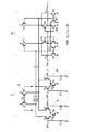
- FIG. 1 is a circuit diagram of the comparator 1 according to the first embodiment.
- the comparator 1 of FIG. 1 is used in, for example, a sequential comparison type ADC, but the application of the comparator 1 of FIG. 1 is not necessarily limited to the ADC.
- Two differential input signal pairs (hereinafter, referred to as a first differential input signal pair and a second differential input signal pair) Vin_p, Vin_n, Vns_p, and Vns_n are input to the comparator 1 of FIG.
- the comparator 1 outputs the differential output signal pairs Vout_p and Vout_n corresponding to the difference signal of the first differential input signal pair Vin_p and Vin_n and the difference signal of the second differential input signal pair Vns_p and Vns_n.
- the comparator 1 of FIG. 1 is a dynamic comparator 1 that performs a comparison operation of two differential input signal pairs Vin_p, Vin_n, Vns_p, and Vns_n.
- the first comparison circuit 2 includes the difference signal between the first differential input signal pair Vin_p and Vin_n generated by connecting the first input terminal TL1 to the positive side and the second input terminal TL2 to the negative side. Outputs a signal corresponding to the difference signal between the second differential input signal pair Vns_p and Vns_n generated by connecting the third input terminal TL3 to the positive side and connecting the fourth input terminal TL4 to the negative side. ..
- the second comparison circuit 3 includes the difference signal between the first differential input signal pair Vin_p and Vin_n generated by connecting the first input terminal TL1 to the negative side and the second input terminal TL2 to the positive side. Outputs a signal corresponding to the difference signal between the second differential input signal pair Vns_p and Vns_n generated by connecting the third input terminal TL3 to the positive side and connecting the fourth input terminal TL4 to the negative side. ..
- the first comparison circuit 2 and the second comparison circuit 3 have a common circuit configuration and common electrical characteristics. More specifically, the corresponding transistors in the first comparison circuit 2 and the second comparison circuit 3 have a common gate width and gate length.
- the first comparison circuit 2 responds to the difference signal between the first differential input signal pair Vin_p and Vin_n generated by connecting the first input terminal TL1 to the positive side and the second input terminal TL2 to the negative side.
- the first differential output signal pair is output from the first output node n1 and the second output node n2.
- the voltage fluctuation amount of the third input terminal TL3 generated in response to the voltage fluctuation of the first output node n1 is equal to the voltage fluctuation amount of the fourth input terminal TL4 generated in response to the voltage fluctuation of the second output node n2.
- the second comparison circuit 3 does not directly participate in the comparison operation of the comparator 1, but acts as a dummy circuit.
- the first comparator circuit 2 has a first comparator 4 and a second comparator 5.
- the first comparator 4 responds to the difference signal between the first differential input signal pair Vin_p and Vin_n generated by connecting the first input terminal TL1 to the positive side and the second input terminal TL2 to the negative side.
- the first differential output signal pair is output from the first output node n1 and the second output node n2.
- the third input terminal TL3 is connected to the positive side and the fourth input terminal TL4 is connected to the negative side, and the second comparator 5 responds to the difference signal of the second differential input signal pair generated.
- the differential output signal pair is output from the first output node n1 and the second output node n2.
- the first comparator 4 has N-type MOS transistors Q1 and Q2.
- the first differential input signal Vin_p is input to the gate of the transistor Q1.
- the gate of transistor Q1 is on the positive side.
- the first differential input signal Vin_n is input to the gate of the transistor Q2.
- the gate of transistor Q2 is on the negative side.
- An N-type MOS transistor Q3 is connected between each source of the transistors Q1 and Q2 and the ground node.
- a clock signal Clk is input to the gate of the transistor Q3.
- the transistors Q1 and Q2 perform a comparison operation between the first differential input signal vs. Vin_p and Vin_n, and when the clock signal Clk is at a low level, the comparison operation is stopped.
- the drain of the transistor Q1 is connected to the first output node n1, and the drain of the transistor Q2 is connected to the second output node n2.
- the second comparator 5 has N-type MOS transistors Q4 and Q5.
- the first differential input signal Vns_p is input to the gate of the transistor Q4.
- the gate of Transis Q4 is on the positive side.
- the second differential input signal Vns_n is input to the gate of the transistor Q5.
- the gate of transistor Q5 is on the negative side.
- An N-type MOS transistor Q6 is connected between the source of the transistors Q4 and Q5 and the ground node.
- a clock signal Clk is input to the gate of the transistor Q6.
- the transistors Q1 and Q2 perform a comparison operation between the first differential input signal vs. Vin_p and Vin_n, and when the clock signal Clk is at a low level, the comparison operation is stopped.
- Each drain of the transistors Q4 and Q5 is connected to the first output node n1 and the second output node n2.
- a pull-up circuit (first voltage setting circuit) 6 is connected to the first output node n1 and the second output node n2.
- the pull-up circuit 6 pulls up the first output node n1 and the second output node n2 to a high level when the clock signal Clk is at a low level, that is, within a period during which the first comparison circuit 2 does not perform the comparison operation.
- the pull-up circuit 6 has a P-type MOS transistor Q7 connected to the first output node n1 and a P-type MOS transistor Q8 connected to the second output node n2.
- a clock signal Clk is input to the gates of the transistors Q7 and Q8.
- the second comparator circuit 3 has a third comparator 7 and a fourth comparator 8.
- the third comparator 7 responds to the difference signal between the first differential input signal pair Vin_p and Vin_n generated by connecting the second input terminal TL2 to the positive side and connecting the first input terminal TL1 to the negative side.
- the third differential output signal pair is output from the first internal node n3 and the second internal node n4.
- the third input terminal TL3 is connected to the positive side and the fourth input terminal TL4 is connected to the negative side to generate a fourth differential input signal pair according to the difference signal.
- the differential output signal pair is output from the first internal node n3 and the second internal node n4.
- the third comparator 7 has N-type MOS transistors Q9 and Q10.
- the first differential input signal Vin_n is input to the gate of the transistor Q9.
- the gate of transistor Q9 is on the positive side.
- the first differential input signal Vin_p is input to the gate of the transistor Q10.
- the gate of transistor Q10 is on the negative side.
- An N-type MOS transistor Q11 is connected between the source of the transistors Q9 and Q10 and the ground node.
- a clock signal Clk is input to the gate of the transistor Q11.
- the transistors Q9 and Q10 perform a comparison operation between the first differential input signal vs. Vin_p and Vin_n, and when the clock signal Clk is at a low level, the comparison operation is stopped.
- the drain of the transistor Q9 is connected to the first internal node n3, and the drain of the transistor Q10 is connected to the second internal node n4.
- the fourth comparator 8 has N-type MOS transistors Q12 and Q13.
- the second differential input signal Vns_p is input to the gate of the transistor Q12.
- the gate of transistor Q12 is on the positive side.
- the second differential input signal Vns_n is input to the gate of the transistor Q13.
- the gate of transistor Q13 is on the negative side.
- An N-type MOS transistor Q14 is connected between the source of the transistors Q12 and Q13 and the ground node.
- a clock signal Clk is input to the gate of the transistor Q14.
- the transistors Q12 and Q13 perform a comparison operation between the first differential input signal vs. Vin_p and Vin_n, and when the clock signal Clk is at a low level, the comparison operation is stopped.
- the drains of the transistors Q12 and Q13 are connected to the first internal node n3 and the second internal node n4.
- a pull-up circuit 9 (second voltage setting circuit) is connected to the first internal node n3 and the second internal node n4.
- the pull-up circuit 9 pulls up the first internal node n3 and the second internal node n4 to a high level when the clock signal Clk is at a low level.
- the pull-up circuit 9 has a P-type MOS transistor Q15 connected to the first internal node n3 and a P-type MOS transistor Q16 connected to the second internal node n4.
- a clock signal Clk is input to the gates of the transistors Q15 and Q16.
- the first internal node n3 and the second internal node n4 of the second comparison circuit 3 acting as a dummy circuit are not connected to anything other than the dummy circuit.
- the first output node n1 and the second output node n2 of the first comparison circuit 2 are connected to the latch circuit 10.
- the latch circuit 10 holds a signal indicating the comparison result output from the first comparison circuit 2 at the timing when the clock signal Clk transitions from the high level to the low level.
- the latch circuit 10 has P-type MOS transistors Q17 to Q20 and N-type MOS transistors Q21 to Q26.
- the first output node n1 is connected to each gate of the transistors Q17, Q21 and Q22.
- the second output node n2 is connected to each gate of the transistors Q18, Q24 and Q25.
- the gates of the transistors Q20 and Q26 and the drains of the transistors Q19 and Q23 are connected to the output terminal TL5 that outputs the differential output voltage Vout_p of the comparator 1.
- the gates of the transistors Q19 and Q23 and the drains of the transistors Q25 and Q26 are connected to the output terminal TL6 that outputs the differential output voltage Vout_n of the comparator 1.
- Comparator 1 in FIG. 1 starts a comparison operation when the clock signal Clk transitions from a low level to a high level. While the clock signal Clk is low level, the first output node n1 and the second output node n2 are pulled up to the power supply voltage level. When the clock signal Clk transitions to a high level, the voltage levels of the first output node n1 and the second output node n2 decrease as the transistors Q1, Q2, Q4, and Q5 are turned on. When Vin_p + Vns_p> Vin_n + Vns_n, the discharge rate of Vgm_p> the discharge rate of Vgm_n. On the contrary, when Vin_p + Vns_p ⁇ Vin_n + Vns_n, the discharge rate of Vgm_p is less than the discharge rate of Vgm_n.
- FIG. 2A and 2B are waveform diagrams of Vgm_p and Vgm_n during the comparative operation of the comparator 1.
- FIG. 2A is a waveform diagram when Vin_p + Vns_p> Vin_n + Vns_n
- FIG. 2B is a waveform diagram when Vin_p + Vns_p ⁇ Vin_n + Vns_n.
- the first differential input signal pair Vin_p, the signal Vin_p on the positive phase side of Vin_n is connected to the gate of the transistor Q1 on the positive phase side of the first comparator 4 in the first comparison circuit 2. At the same time, it is connected to the gate of the transistor Q10 on the negative phase side of the third comparator 7 in the second comparator circuit 3. Further, the signals Vin_n on the negative phase side of the first differential input signal pair Vin_p and Vin_n are connected to the gate of the transistor Q2 on the negative phase side of the first comparator 4 in the first comparator circuit 2, and the second comparison is performed. It is connected to the gate of the transistor Q9 on the positive phase side of the fourth comparator 8 in the circuit 3. In this way, in the first comparison circuit 2 and the second comparison circuit 3, the connection destinations of the first differential input signal pair Vin_p and Vin_n are reversed.
- the voltage level of the first output node n1 and the second output node n2 from which the comparison result of the first comparison circuit 2 is output varies greatly depending on the comparison result of the first comparison circuit 2.
- the transistors Q1 or Q2 in FIG. 1 are turned on, the voltage level of the first output node n1 or the second output node n2 is lowered by discharge.
- the transistor Q1 or Q2 of the transistor Q1 or Q2 passes through the parasitic capacitance of the MOS of the transistor Q1 or Q2 in the first comparison circuit 2.
- a so-called kickback current in which a current flows through the gate, may occur.
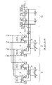
- FIG. 3 is a circuit diagram of a sequential comparison type ADC 11 provided with the comparator 1 of FIG.
- the sequential comparison type ADC 11 of FIG. 3 shows an example of converting a differential input signal pair into a 5-bit digital signal.
- the number of bits of the sequential comparison type ADC 11 is arbitrary. Further, the circuit configuration of the sequential comparison type ADC 11 is not limited to that shown in FIG.
- the sequential comparison type ADC 11 of FIG. 3 includes a first sampling switch 12, a second sampling switch 13, a first digital-analog converter (hereinafter, first DAC) 14, and a second digital-analog converter (second DAC 15).
- a filter circuit 16, a comparator 1, and a control circuit (SAR logic) 17 are provided.
- the first DAC14 and the second DAC15 are collectively referred to as a capacitance DAC18.
- the first sampling switch 12 switches whether or not to sample one of the differential input signal vs. Vad_p and Vad_n signals, Vad_p.
- the second sampling switch 13 switches whether or not to sample the other signal Vad_n of the differential input signal pair Vad_p and Vad_n.
- the first DAC 14 converts one of the sampled signals Vad_p into a digital signal consisting of a plurality of bits in order bit by bit, and outputs a signal of a voltage level corresponding to the unconverted bits.
- the first DAC 14 has five capacitors C1 to C5 having different capacities by a power of two, and three switches (first to third switches) SW1 to SW3 connected to the capacitors C1 to C5.
- the first switch SW1 switches whether or not one end of the capacitor is set to 0V.
- the second switch SW2 switches whether or not one end of the capacitor is set to the common voltage Vcom.
- the third switch SW3 switches whether or not one end of the capacitor is set to the reference voltage Vref.
- the common voltage Vcom is, for example, a voltage level of 1/2 of the reference voltage Vref.
- the first to third switches SW1 to SW3 are switched on or off based on the control signal from the control circuit 17.
- the control circuit 17 turns on the second switch SW2 at the start of the comparison operation. After that, the control circuit 17 turns on the first switch SW1 when it wants to lower the output node voltage Vin_p of the first DAC 14, and turns on the third switch SW3 when it wants to raise the output node voltage Vin_p of the first DAC 14.
- the second DAC 15 sequentially converts the other sampled signal into a digital signal composed of a plurality of bits one bit at a time, and outputs a signal with a voltage level corresponding to the unconverted bits.
- the second DAC 15 is configured in the same manner as the first DAC 14, and switches the first to third switches SW1 to SW3 based on the control signal from the control circuit 17 in the same manner as the first DAC 14.
- the filter circuit 16 samples and outputs the output signal of the first DAC 14 and the output signal of the second DAC 15.
- Comparator 1 has the configuration shown in FIG.
- the comparator 1 has a first differential input signal pair Vin_p, Vin_n that pairs an output signal of the first DAC 14 and an output signal of the second DAC 15, and a second differential input signal pair Vns_p, Vns_n output from the filter circuit 16. Is entered.
- the comparator 1 outputs a signal corresponding to the difference signal between the first differential input signal vs. Vin_p and Vin_n and the difference signal between the second differential input signal vs. Vns_p and Vns_n.
- the control circuit 17 performs switching control of the first to third switches SW1 to SW3 in the first DAC14 and the second DAC15 based on the output signal of the comparator 1.
- FIG. 4 is a voltage waveform diagram of the output node voltage Vin_p of the first DAC 14 and the output node voltage Vin_n of the second DAC 15 of FIG.
- both the first sampling switch 12 and the second sampling switch 13 are turned on to sample the differential input signal pairs Vad_p and Vad_n.
- one end of each of the capacitors C1 to C5 is set to the common voltage Vcom via the second switch SW2.
- the electric charge corresponding to the difference signal between the differential input signal vs. Vad_p and Vad_n is accumulated in the capacitance DAC18.
- the output signal of the first DAC 14 and the output signal of the second DAC 15 constituting the capacitance DAC 18 are the first differential input signal pair Vin_p and Vin_n input to the comparator 1.
- the differential output signal of the filter circuit 16 is the second differential input signal pair Vns_p and Vns_n input to the comparator 1.
- both the first sampling switch 12 and the second sampling switch 13 are turned off, and the comparison operation by the comparator 1 is started.
- the output of the capacitance DAC 18 is controlled so that the output voltage becomes smaller in order from the above bits according to the sampled differential input signal vs. the difference signal of Vad_p and Vad_n, and the output voltage gradually approaches zero.
- the voltage remaining in the capacitance DAC 18 is sampled by the filter circuit 16 to change the output voltage of the filter circuit 16.
- the residual voltage at the completion of control of the capacitance DAC 18 is a very small voltage level, and the filter circuit 16 continues to output a signal with a small voltage level. That is, the state of the difference signal (Vns_p ⁇ Vns_n) ⁇ 0 between the second differential input signal vs. Vns_p and Vns_n is maintained. Therefore, when the comparator 1 of FIG. 1 is used in the ADC 11 of FIG. 3, the difference between the discharge rates of the voltage Vgm_p of the first output node n1 of FIG. 1 and the voltage Vgm_n of the second output node n2 is the first differential input signal. It is almost determined only by the difference signal between Vin_p and Vin_n.
- the comparator 1 of FIG. 1 when the voltage Vgm_p of the first output node n1 and the voltage Vgm_n of the second output node n2 are discharged, the gates of the transistors Q1 and Q2 in the first comparator 4 and the second A kickback current flows through the gates of transistors Q4 and Q5 in the comparator 5.
- the waveform of the kickback current changes greatly depending on the discharge rate of the voltage Vgm_p of the first output node n1 and the voltage Vgm_n of the second output node n2.
- the first differential input signal pairs Vin_p and Vin_n input to the comparator 1 are connected to the output node of the capacitance DAC18, and there are a plurality of capacitors C1 to C5 in the capacitance DAC18. Even if a kickback current flows through the gates of the transistors Q1 and Q2 in the first comparator 4 of No. 1, the voltage fluctuations of the first differential input signal pair Vin_p and Vin_n are not large. On the other hand, since the output node of the filter circuit 16 to which the second differential input signal pair Vns_p and Vns_s are connected does not have a large capacitor, it kicks to the gate of the transistors Q4 and Q5 in the second comparator 5 of FIG. When the back current flows, the voltage fluctuations of the second differential input signal vs. Vns_p and Vns_s may become relatively large due to the influence.
- the discharge of the differential output voltages vs. Vgm_p and Vgm_n of the first and second output nodes n1 and n2 causes a kickback to the second differential input signals vs. Vns_p and Vns_n.
- Vin_p Vin_n
- Vns_p and Vns_n are the same, and the difference signal (Vns_p-Vns_n) of the second differential input signal vs. Vns_p and Vns_n does not fluctuate.
- Vin_p Vin_n
- the discharge rate is different, and the kickback current waveforms for the second differential input signal vs. Vns_p and Vns_n are also different. Therefore, it appears as a change in the difference signal (Vns_p-Vns_n) between the second differential input signal vs. Vns_p and Vns_n.
- Vin_p and Vin_n the larger the difference in discharge rate. Also becomes large, and the change of the difference signal (Vns_p-Vns_n) between the second differential input signal vs. Vns_p and Vns_n becomes large.
- the output signal level of the filter circuit 16 is essentially a small voltage level. If there is a voltage fluctuation in the output signal level of the filter circuit 16 due to kickback, there is a risk that the ADC 11 will not operate as desired, and the characteristics of the ADC 11 itself will be deteriorated. Further, if the output impedance of the filter circuit 16 is lowered in order to reduce the voltage fluctuation, the design of the filter circuit 16 itself becomes difficult, such as an increase in current consumption.
- the connection destinations of the first differential input signal pair Vin_p and Vin_n are reversed.
- the voltage fluctuation due to the kickback of one signal Vns_p of the second differential input signal vs. Vns_p and Vns_n and the voltage fluctuation due to the kickback of the other signal Vns_n of the second differential input signal vs. Vns_p and Vns_n. Can be made equal, and the voltage fluctuation due to kickback of each gate of the transistors Q4 and Q5 in the second comparator 5 can be offset. This will be described in more detail.
- the kickback current from the voltage Vgm_p of the first output node n1 to the second differential input signal Vns_p is I ⁇
- the kickback current from the voltage Vgm_n of the second output node n2 to the second differential input signal Vns_n is I ⁇
- the difference between the kickback currents of the second differential input signal pair Vns_p and Vns_n when the second comparator circuit 3 which is a dummy circuit does not exist is I ⁇ -I ⁇ .
- the discharge rate of the second internal node n4 voltage Vgm_dmy_n in the second comparison circuit 3 which is a dummy circuit is the same as the discharge rate of the first internal node n3 voltage Vgm_dmy_p. Therefore, the kickback current from the second internal node n4 voltage Vgm_dmy_n to the second differential input signal Vns_n is I ⁇ . Similarly, the kickback current from the first internal node n3 voltage Vgm_dmy_p to the second differential input signal Vns_p is I ⁇ .
- the kickback current to the second differential input signal Vns_p is I ⁇ + I ⁇
- the fact that the difference in kickback current is zero means that fluctuations due to kickback of the second differential input signals Vns_p and Vns_n of the comparator 1 are eliminated.
- the first comparator 4 in the first comparison circuit 2 and the third comparator 7 in the second comparison circuit 3 have the first differential input signal pair Vin_p and Vin_n. Since the connection destinations of the positive phase side and negative phase side signals are reversed from each other, the discharge of the first output node n1 and the second output node n2 kicks back to the gates of the transistors Q4 and Q5 in the second comparator 5. Even if a current flows, the kickback current flowing through the gates of the transistors Q4 and Q5 can be made equal, so that the voltage fluctuations due to the kickback current cancel each other out, and the first output node n1 and the second output node n2 kickback. It is no longer affected by electric current.
- FIG. 5 is a circuit diagram of the comparator 100 according to a comparative example.
- the comparator 100 of FIG. 5 includes the first comparison circuit 2 and the latch circuit 10 of FIG. 1, but does not have the second comparison circuit 3.
- the kickback current from the voltage Vgm_p of the first output node n1 to the second differential input signal Vns_p is I ⁇
- the kickback current from the voltage Vgm_n of the second output node n2 to the second differential input signal Vns_n is I ⁇
- the difference in kickback current between the gates of the transistors Q4 and Q5 in the second comparator 5 is I ⁇ -I ⁇ because the second comparator circuit 3 which is a dummy circuit does not exist, and is zero. It does not become. Therefore, in the comparator 100 of FIG. 5, when the voltage levels of the voltage Vgm_p of the first output node n1 and the voltage Vgm_n of the second output node n2 fluctuate depending on the discharge rate, the difference in kickback current (I ⁇ -) according to the fluctuations. I ⁇ ) occurs, and the differential output voltages Vgm_p and Vgm_n of the comparator 100 fluctuate according to the difference.
- FIG. 6A is a signal waveform diagram of each part in the comparator 1 of FIG. 1 by simulation
- FIG. 6B is a signal waveform diagram of each part in the comparator 100 of FIG. 5 by simulation.
- 6A and 6B show the voltage waveform of the clock signal Clk, the voltage waveform of the first differential input signal pair Vin_p, Vin_n difference signal (Vin_p-Vin_n), and the second differential input signal pair Vns_p, Vns_n.
- the voltage waveform of the difference signal (Vns_p-Vns_n) is shown in the figure.
- the comparators 1 and 100 start the comparison operation at time t1.
- the control circuit 17 determines the charge charge of the capacitor of the capacitance DAC 18 in order from the upper side so that the output voltage (Vin_p-Vin_n) of the capacitance DAC 18 becomes zero.
- the output signal (Vns_p-Vns_n) of the filter circuit 16 is approximately 0 V in FIG. 6A, whereas in FIG. 6B, a large spike-like voltage fluctuation occurs every time the comparator 100 performs a comparison operation. More specifically, in the simulation result of FIG. 6A, the output voltage of the filter circuit 16 is a minute DC voltage of about 300 ⁇ V, whereas in FIG. 6B, a very large spike-like voltage fluctuation occurs. It may exceed 1 mV at the maximum.
- the output voltage of the filter circuit 16 is kept constant during the comparison operation. If the output voltage of the filter circuit 16 fluctuates, the analog-to-digital conversion operation may not be performed normally, and the characteristics of the ADC 11 itself are deteriorated.
- the comparator 1 is different from the first comparison circuit 2 in which the first differential input signal pair Vin_p, Vin_n and the second differential input signal pair Vns_p, Vns_n are input.
- a second comparison circuit 3 which is a dummy circuit having the same circuit configuration and the same electrical characteristics as the first comparison circuit 2, is provided.
- the first differential input signal pair Vin_p and Vin_n are provided. Reverse the connection destinations. More specifically, in the first comparator 4 in the first comparator circuit 2, the signals on the positive phase side of the first differential input signal pair Vin_p and Vin_n are input to the gate of the transistor on the positive phase side.
- the signals on the positive phase side of the first differential input signal pair Vin_p and Vin_n are input to the gate of the transistor on the negative phase side.
- a kickback current flows through the gates of the transistors Q4 and Q5 in the second comparator 5 due to the voltage fluctuations of the voltages Vgm_p and Vgm_n of the first output node n1 and the second output node n2 of the first comparator circuit 2.
- the voltage fluctuations due to the kickback current at the gates of the transistors Q4 and Q5 can be made equal.
- the voltages Vgm_p and Vgm_n of the first output node n1 and the second output node n2 do not cause voltage fluctuation due to the kickback current, the output voltage of the comparator 1 can be stabilized, and the performance deterioration of the ADC 11 can be suppressed.
- the first comparator 4 and the second comparator 5 in the first comparison circuit 2 and the third comparator 7 and the fourth comparator 8 in the second comparison circuit 3 are N-type MOS transistors. However, it may be composed of a P-type MOS transistor.
- FIG. 7 is a circuit diagram of the comparator 1a according to the second embodiment.
- the comparator 1a of FIG. 7 is obtained by reversing the conductive type of each transistor in the comparator 1 of FIG. 1, and has transistors Q31 to Q38, Q41 to Q46, and Q51 to Q56.
- the first comparator 4 and the second comparator 5 in the first comparison circuit 2 in the comparator 1a of FIG. 7 are composed of P-type MOS transistors Q31 to Q36.
- the pull-up circuit 6 is composed of N-type MOS transistors Q37 and Q38.
- the conductive type of each transistor Q51 to Q56 in the latch circuit 10 is also opposite to that of the latch circuit 10 of FIG.
- the comparator 1a of FIG. 7 similarly to the comparator 1 of FIG. 1, in the first comparator 4 in the first comparison circuit 2 and the third comparator 7 in the second comparison circuit 3, the first differential input signal.
- the connection destinations of the positive side signal and the negative side signal of Vin_p and Vin_n are opposite to each other. Therefore, also in the comparator 1a of FIG. 7, similarly to the comparator 1 of FIG. 1, the transistors Q4 in the second comparator 5 are caused by the voltage fluctuations of the voltages Vgm_p and Vgm_n of the first output node n1 and the second output node n2. Even if a kickback current flows through the gate of Q5, the voltages Vgm_p and Vgm_n do not fluctuate due to the kickback current, and the performance deterioration of the ADC 11 can be suppressed.
- the third embodiment has a different configuration of the latch circuit 10 from the first embodiment.
- FIG. 8 is a circuit diagram of the comparator 1b according to the third embodiment.
- the comparator 1b of FIG. 8 includes a first comparison circuit 2 and a second comparison circuit 3 having the same circuit configuration as the comparator 1 of FIG.
- the comparator 1b of FIG. 8 includes a first latch circuit 21 connected to a first output node n1 and a second output node n2 of the first comparison circuit 2, and a first internal node n3 and a second internal of the second comparison circuit 3. It includes a second latch circuit 22 connected to the node n4.
- the first latch circuit 21 has P-type MOS transistors Q61 to Q64 and N-type MOS transistors Q65 and Q66.
- a clock signal Clk is input to each gate of the transistors Q61 and Q63.
- the gates of the transistors Q62 and Q65 and the drains of the transistors Q63 and Q64 are connected to the output node voltage Vout_p.
- the gates of the transistors Q64 and Q66 and the drains of the transistors Q62 and Q65 are connected to the output node voltage Vout_n.
- the source of the transistor Q65 is connected to the voltage Vgm_p of the first output node n1
- the source of the transistor Q66 is connected to the voltage Vgm_n of the second output node n2.
- the second latch circuit 22 has P-type MOS transistors Q71 to Q74 and N-type MOS transistors Q75 and Q76, and is configured in the same manner as the first latch circuit 21.
- the comparator 1b in FIG. 8 starts the comparison operation. After that, when the clock signal Clk transitions from the high level to the low level, the first latch circuit 21 holds the comparison result by the first comparison circuit 2, and the second latch circuit 22 holds the comparison result by the second comparison circuit 3. Hold.
- the comparator 1b of FIG. 8 is a first differential input signal in the first comparator 4 in the first comparison circuit 2 and the third comparator 7 in the second comparison circuit 3.
- the connection destinations of the positive side signal and the negative side signal of Vin_p and Vin_n are opposite to each other. Therefore, also in the comparator 1b of FIG. 8, similarly to the comparator 1 of FIG. 1, the transistors Q4 in the second comparator 5 are caused by the voltage fluctuations of the voltages Vgm_p and Vgm_n of the first output node n1 and the second output node n2. Even if a kickback current flows through the gate of Q5, the voltages Vgm_p and Vgm_n do not fluctuate due to the kickback current, and the performance deterioration of the ADC 11 can be suppressed.
- the comparator 1c according to the fourth embodiment is for inputting the signal output from the first comparison circuit 2 to the latch circuit 10 after waveform shaping.
- FIG. 9 is a circuit diagram of the comparator 1c according to the fourth embodiment.
- the comparator 1c of FIG. 9 includes a first comparison circuit 2, a second comparison circuit 3, and a latch circuit 10 having the same configuration as the comparator 1 of FIG.
- the comparator 1c of FIG. 9 includes inverters 23 and 24.
- the inverters 23 and 24 are connected to the first output node n1 and the second output node n2 connected to the first comparison circuit 2, respectively.
- the inverters 23 and 24 invert the logic of the input signal and output it. At that time, the inverters 23 and 24 perform waveform shaping to make the output signal waveform steep. In this way, the inverters 23 and 24 operate as a waveform shaping circuit.
- various logical operation elements for example, NAND element, NOR element, etc. may be used.
- the voltage levels of the voltages Vgm_p and Vgm_n of the first output node n1 and the second output node n2 decrease due to the discharge by the transistors Q1, Q2, Q4, and Q5 in the first comparator 4 and the second comparator 5.
- the inverters 23 and 24 are charged as the voltages Vgm_p and Vgm_n of the first output node n1 and the second output node n2 are discharged.
- the latch circuit 10 performs a holding operation according to the logic according to the difference in charging speed between the output voltages of the inverters 23 and 24.
- the comparator 1c of FIG. 9 is a first differential input signal in the first comparator 4 in the first comparison circuit 2 and the third comparator 7 in the second comparison circuit 3.
- the connection destinations of the positive side signal and the negative side signal of Vin_p and Vin_n are opposite to each other. Therefore, also in the comparator 1b of FIG. 8, similarly to the comparator 1 of FIG. 1, the transistors Q4 in the second comparator 5 are caused by the voltage fluctuations of the voltages Vgm_p and Vgm_n of the first output node n1 and the second output node n2. Even if a kickback current flows through the gate of Q5, the voltages Vgm_p and Vgm_n do not fluctuate due to the kickback current, and the performance deterioration of the ADC 11 can be suppressed.
- the waveform shaping circuit by the inverters 23, 24 and the like of FIG. 9 may be provided in the comparators 1a and 1b of FIG. 7 or FIG.
- the output signal of the first comparator circuit 2 is once waveform-shaped by the inverters 23, 24 and the like, and then the latch circuit 10 performs the holding operation. Therefore, the latch circuit 10 quickly performs the holding operation.
- the operation speed of the comparator 1c shown in FIG. 9 can be improved.
- the technical features common to the comparators 1, 1a, 1b, and 1c according to the first to fourth embodiments described above are that the second comparison circuit 3 having the same circuit configuration and the same electrical characteristics as the first comparison circuit 2 is provided.
- the connection destinations of the first differential input signal pair Vin_p and Vin_n are reversed.
- fluctuations in the voltages Vgm_p and Vgm_n of the first output node n1 and the second output node n2 of the first comparison circuit 2 due to the kickback current can be suppressed.
- the present technology can have the following configurations. (1) The first input terminal and the second input terminal to which the first differential input signal pair is input, and The third input terminal and the fourth input terminal to which the second differential input signal pair is input, and The difference signal of the first differential input signal pair generated by connecting the first input terminal to the positive side and connecting the second input terminal to the negative side, and the third input terminal to the positive side.
- a first comparison circuit that outputs a signal corresponding to the difference signal of the second differential input signal pair generated by connecting and connecting the fourth input terminal to the negative side. The difference signal of the first differential input signal pair generated by connecting the first input terminal to the negative side and connecting the second input terminal to the positive side, and the third input terminal to the positive side.
- the comparator according to (1) comprising a first output terminal and a second output terminal for outputting a differential output signal pair corresponding to the signal output from the first comparison circuit.
- the comparator according to (1) or (2) wherein the voltage level of the difference signal of the first differential input signal pair is larger than the voltage level of the difference signal of the second differential input signal pair.
- the first comparison circuit is a first output node that differentially outputs a signal corresponding to the difference signal of the first differential input signal pair and the difference signal of the second differential input signal pair. And has a second output node
- the voltage fluctuation amount of the third input terminal generated in response to the voltage fluctuation of the first output node is equal to the voltage fluctuation amount of the fourth input terminal generated in response to the voltage fluctuation of the second output node, (1).
- the comparator according to any one of (4) to (4).
- the first comparison circuit is A first differential output signal pair corresponding to the difference signal of the first differential input signal pair generated by connecting the first input terminal to the positive side and connecting the second input terminal to the negative side.
- the first comparator that outputs to the first output node and the second output node, and A second differential output signal pair corresponding to the difference signal of the second differential input signal pair generated by connecting the third input terminal to the positive side and connecting the fourth input terminal to the negative side is provided. It has a first output node and a second comparator that outputs from the second output node.
- the second comparison circuit is A third differential output signal pair corresponding to the difference signal of the first differential input signal pair generated by connecting the second input terminal to the positive side and connecting the first input terminal to the negative side is provided.
- a third comparator that outputs to the first internal node and the second internal node, A fourth differential output signal pair corresponding to the difference signal of the second differential input signal pair generated by connecting the third input terminal to the positive side and connecting the fourth input terminal to the negative side is provided.
- the comparator according to (5) further comprising a first internal node and a fourth comparator that outputs from the second internal node.
- a first voltage setting circuit that sets the first output node and the second output node to a predetermined voltage level within a period in which the first comparison circuit does not perform a comparison operation.
- the second voltage setting circuit is provided, wherein the first internal node and the second internal node are set to a predetermined voltage level within a period in which the second comparison circuit does not perform the comparison operation, according to (6).
- comparator Each of the first comparator, the second comparator, the third comparator, and the fourth comparator has an N-type transistor.
- Each of the first comparator, the second comparator, the third comparator, and the fourth comparator has a P-type transistor.
- the comparator according to (7), wherein each of the first voltage setting circuit and the second voltage setting circuit has an N-type transistor.
- the first comparator, the second comparator, the third comparator, and the fourth comparator perform a comparison operation when the predetermined signal is the first logic, and the predetermined signal is generated. In the case of the second logic, the comparison operation is stopped and the comparison operation is stopped.
- the first voltage setting circuit sets the first output node and the second output node to the predetermined voltage level when the predetermined signal is the second logic.
- the second voltage setting circuit sets the first internal node and the second internal node to the predetermined voltage level when the predetermined signal is the second logic, according to (7) to (9).
- the comparator according to any one item.
- a first sampling switch that switches whether to sample one signal of the differential input signal pair, and A first digital-to-analog converter that converts one of the sampled signals into a digital signal consisting of a plurality of bits in order bit by bit and outputs a signal with a voltage level corresponding to the unconverted bits.
- a second sampling switch that switches whether to sample the other signal of the differential input signal pair, and A second digital-to-analog converter that converts the other sampled signal into a digital signal consisting of a plurality of bits in order bit by bit and outputs a signal with a voltage level corresponding to the unconverted bits.
- a filter circuit that samples and outputs the output signal of the first digital-to-analog converter and the output signal of the second digital-to-analog converter.
- the difference signal of the first differential input signal pair that pairs the output signal of the first digital-analog converter and the output signal of the second digital-analog converter, and the second difference output from the filter circuit.
- a comparator that outputs the difference signal of the dynamic input signal pair and the corresponding signal, and The comparator includes a control circuit for controlling the first digital-to-analog converter and the second digital-to-analog converter based on the output signal of the comparator.
- a first comparison circuit that outputs a signal corresponding to the difference signal of the second differential input signal pair generated by connecting and connecting the fourth input terminal to the negative side.
Landscapes
- Engineering & Computer Science (AREA)
- Theoretical Computer Science (AREA)
- Manipulation Of Pulses (AREA)
- Analogue/Digital Conversion (AREA)
Priority Applications (2)
| Application Number | Priority Date | Filing Date | Title |
|---|---|---|---|
| US17/906,663 US12107595B2 (en) | 2020-03-30 | 2021-03-23 | Comparator and analog-to-digital converter |
| JP2022511996A JP7762141B2 (ja) | 2020-03-30 | 2021-03-23 | コンパレータ及びアナログ-デジタル変換器 |
Applications Claiming Priority (2)
| Application Number | Priority Date | Filing Date | Title |
|---|---|---|---|
| JP2020-061363 | 2020-03-30 | ||
| JP2020061363 | 2020-03-30 |
Publications (1)
| Publication Number | Publication Date |
|---|---|
| WO2021200416A1 true WO2021200416A1 (ja) | 2021-10-07 |
Family
ID=77927087
Family Applications (1)
| Application Number | Title | Priority Date | Filing Date |
|---|---|---|---|
| PCT/JP2021/012087 Ceased WO2021200416A1 (ja) | 2020-03-30 | 2021-03-23 | コンパレータ及びアナログ-デジタル変換器 |
Country Status (3)
| Country | Link |
|---|---|
| US (1) | US12107595B2 (https=) |
| JP (1) | JP7762141B2 (https=) |
| WO (1) | WO2021200416A1 (https=) |
Cited By (2)
| Publication number | Priority date | Publication date | Assignee | Title |
|---|---|---|---|---|
| US20220376685A1 (en) * | 2021-05-24 | 2022-11-24 | Mediatek Inc. | Gain-boosted comparator |
| JP2024542441A (ja) * | 2021-11-24 | 2024-11-15 | セインチップス テクノロジー カンパニーリミテッド | パイプライン逐次比較型アナログデジタル変換器、集積回路および電子機器 |
Citations (1)
| Publication number | Priority date | Publication date | Assignee | Title |
|---|---|---|---|---|
| JP2011061337A (ja) * | 2009-09-08 | 2011-03-24 | Ricoh Co Ltd | ヒステリシスコンパレータ |
Family Cites Families (2)
| Publication number | Priority date | Publication date | Assignee | Title |
|---|---|---|---|---|
| US5148162A (en) * | 1991-04-09 | 1992-09-15 | Tektronix, Inc. | Analog-to-digital converter comparator circuit utilizing a reverse polarity sampling technique |
| US5491448A (en) * | 1994-07-29 | 1996-02-13 | National Semiconductor Corporation | Class AB output stage with improved frequency stability |
-
2021
- 2021-03-23 WO PCT/JP2021/012087 patent/WO2021200416A1/ja not_active Ceased
- 2021-03-23 US US17/906,663 patent/US12107595B2/en active Active
- 2021-03-23 JP JP2022511996A patent/JP7762141B2/ja active Active
Patent Citations (1)
| Publication number | Priority date | Publication date | Assignee | Title |
|---|---|---|---|---|
| JP2011061337A (ja) * | 2009-09-08 | 2011-03-24 | Ricoh Co Ltd | ヒステリシスコンパレータ |
Cited By (4)
| Publication number | Priority date | Publication date | Assignee | Title |
|---|---|---|---|---|
| US20220376685A1 (en) * | 2021-05-24 | 2022-11-24 | Mediatek Inc. | Gain-boosted comparator |
| US11777482B2 (en) * | 2021-05-24 | 2023-10-03 | Mediatek Inc. | Gain-boosted comparator |
| JP2024542441A (ja) * | 2021-11-24 | 2024-11-15 | セインチップス テクノロジー カンパニーリミテッド | パイプライン逐次比較型アナログデジタル変換器、集積回路および電子機器 |
| JP7794968B2 (ja) | 2021-11-24 | 2026-01-06 | セインチップス テクノロジー カンパニーリミテッド | パイプライン逐次比較型アナログデジタル変換器、集積回路および電子機器 |
Also Published As
| Publication number | Publication date |
|---|---|
| US12107595B2 (en) | 2024-10-01 |
| JPWO2021200416A1 (https=) | 2021-10-07 |
| US20230179220A1 (en) | 2023-06-08 |
| JP7762141B2 (ja) | 2025-10-29 |
Similar Documents
| Publication | Publication Date | Title |
|---|---|---|
| JP4705858B2 (ja) | アナログ・ディジタル変換回路 | |
| US8198921B2 (en) | Dynamic comparator with background offset calibration | |
| US8487802B2 (en) | Comparator and analog-to-digital converter | |
| US7265705B1 (en) | Opamp and capacitor sharing scheme for low-power pipeline ADC | |
| CN101179272B (zh) | 斜坡波发生电路和ad变换器 | |
| US6046612A (en) | Self-resetting comparator circuit and method | |
| EP3387751B1 (en) | A double data rate time interpolating quantizer with reduced kickback noise | |
| CN108964665B (zh) | 具有无解码器四元切换的电流导引数模转换器 | |
| US20120139771A1 (en) | Differential successive approximation analog to digital converter | |
| EP0886377B1 (en) | A chopper-type voltage comparator | |
| US7956652B2 (en) | Semiconductor integrated circuit | |
| WO2021200416A1 (ja) | コンパレータ及びアナログ-デジタル変換器 | |
| CN114759911A (zh) | 一种低回踢噪声的可综合动态电压比较器 | |
| CN114257222A (zh) | 一种单时钟控制高速比较器电路 | |
| WO2021200415A1 (ja) | コンパレータ及びアナログ-デジタル変換器 | |
| CN216625715U (zh) | 浮空型动态锁存比较器和逐次逼近型模数转换器 | |
| US8232904B2 (en) | Folding analog-to-digital converter | |
| JP3907633B2 (ja) | Nic回路及びadc回路 | |
| JP7622063B2 (ja) | コンパレータ及びアナログ-デジタル変換器 | |
| JP3597058B2 (ja) | 電圧比較器及びa/d変換器 | |
| KR102435395B1 (ko) | 높은 동적 입력 범위를 위한 샘플링 스위치 및 그의 구동 방법 | |
| JP7518092B2 (ja) | コンパレータ回路およびadコンバータ | |
| JP4639162B2 (ja) | アナログ・ディジタル変換器 | |
| US20070290724A1 (en) | Comparator circuit | |
| WO2017081890A1 (ja) | 電圧変換回路、および、電子装置 |
Legal Events
| Date | Code | Title | Description |
|---|---|---|---|
| 121 | Ep: the epo has been informed by wipo that ep was designated in this application |
Ref document number: 21781176 Country of ref document: EP Kind code of ref document: A1 |
|
| ENP | Entry into the national phase |
Ref document number: 2022511996 Country of ref document: JP Kind code of ref document: A |
|
| NENP | Non-entry into the national phase |
Ref country code: DE |
|
| 122 | Ep: pct application non-entry in european phase |
Ref document number: 21781176 Country of ref document: EP Kind code of ref document: A1 |