WO2021200416A1 - コンパレータ及びアナログ-デジタル変換器 - Google Patents
コンパレータ及びアナログ-デジタル変換器 Download PDFInfo
- Publication number
- WO2021200416A1 WO2021200416A1 PCT/JP2021/012087 JP2021012087W WO2021200416A1 WO 2021200416 A1 WO2021200416 A1 WO 2021200416A1 JP 2021012087 W JP2021012087 W JP 2021012087W WO 2021200416 A1 WO2021200416 A1 WO 2021200416A1
- Authority
- WO
- WIPO (PCT)
- Prior art keywords
- signal
- comparator
- input terminal
- output
- circuit
- Prior art date
Links
Images


Classifications
-
- H—ELECTRICITY
- H03—ELECTRONIC CIRCUITRY
- H03M—CODING; DECODING; CODE CONVERSION IN GENERAL
- H03M1/00—Analogue/digital conversion; Digital/analogue conversion
- H03M1/12—Analogue/digital converters
- H03M1/34—Analogue value compared with reference values
- H03M1/38—Analogue value compared with reference values sequentially only, e.g. successive approximation type
- H03M1/46—Analogue value compared with reference values sequentially only, e.g. successive approximation type with digital/analogue converter for supplying reference values to converter
- H03M1/466—Analogue value compared with reference values sequentially only, e.g. successive approximation type with digital/analogue converter for supplying reference values to converter using switched capacitors
-
- H—ELECTRICITY
- H03—ELECTRONIC CIRCUITRY
- H03M—CODING; DECODING; CODE CONVERSION IN GENERAL
- H03M1/00—Analogue/digital conversion; Digital/analogue conversion
- H03M1/12—Analogue/digital converters
- H03M1/34—Analogue value compared with reference values
- H03M1/38—Analogue value compared with reference values sequentially only, e.g. successive approximation type
- H03M1/46—Analogue value compared with reference values sequentially only, e.g. successive approximation type with digital/analogue converter for supplying reference values to converter
-
- H—ELECTRICITY
- H03—ELECTRONIC CIRCUITRY
- H03M—CODING; DECODING; CODE CONVERSION IN GENERAL
- H03M1/00—Analogue/digital conversion; Digital/analogue conversion
- H03M1/06—Continuously compensating for, or preventing, undesired influence of physical parameters
- H03M1/08—Continuously compensating for, or preventing, undesired influence of physical parameters of noise
- H03M1/0854—Continuously compensating for, or preventing, undesired influence of physical parameters of noise of quantisation noise
-
- H—ELECTRICITY
- H03—ELECTRONIC CIRCUITRY
- H03M—CODING; DECODING; CODE CONVERSION IN GENERAL
- H03M1/00—Analogue/digital conversion; Digital/analogue conversion
- H03M1/06—Continuously compensating for, or preventing, undesired influence of physical parameters
- H03M1/08—Continuously compensating for, or preventing, undesired influence of physical parameters of noise
- H03M1/0863—Continuously compensating for, or preventing, undesired influence of physical parameters of noise of switching transients, e.g. glitches
-
- H—ELECTRICITY
- H03—ELECTRONIC CIRCUITRY
- H03M—CODING; DECODING; CODE CONVERSION IN GENERAL
- H03M1/00—Analogue/digital conversion; Digital/analogue conversion
- H03M1/66—Digital/analogue converters
- H03M1/662—Multiplexed conversion systems
-
- H—ELECTRICITY
- H03—ELECTRONIC CIRCUITRY
- H03M—CODING; DECODING; CODE CONVERSION IN GENERAL
- H03M1/00—Analogue/digital conversion; Digital/analogue conversion
- H03M1/66—Digital/analogue converters
- H03M1/72—Sequential conversion in series-connected stages
-
- H—ELECTRICITY
- H03—ELECTRONIC CIRCUITRY
- H03K—PULSE TECHNIQUE
- H03K5/00—Manipulating of pulses not covered by one of the other main groups of this subclass
- H03K5/22—Circuits having more than one input and one output for comparing pulses or pulse trains with each other according to input signal characteristics, e.g. slope, integral
- H03K5/24—Circuits having more than one input and one output for comparing pulses or pulse trains with each other according to input signal characteristics, e.g. slope, integral the characteristic being amplitude
- H03K5/2472—Circuits having more than one input and one output for comparing pulses or pulse trains with each other according to input signal characteristics, e.g. slope, integral the characteristic being amplitude using field effect transistors
- H03K5/2481—Circuits having more than one input and one output for comparing pulses or pulse trains with each other according to input signal characteristics, e.g. slope, integral the characteristic being amplitude using field effect transistors with at least one differential stage
Definitions
- the present disclosure relates to comparators and analog-to-digital converters.
- a sequential comparison analog-to-digital converter (hereinafter, sequential comparison ADC) equipped with a sampling switch, a comparator to which two differential input signal pairs are input, and a digital-analog converter (hereinafter, DAC) is known.
- sequential comparison ADC sequential comparison analog-to-digital converter
- DAC digital-analog converter
- This type of comparator holds a signal corresponding to the difference signal of one differential input signal pair and the difference signal of the other differential input signal pair.
- the DAC is controlled by the signal held by the comparator, and two differential input signal pairs are generated based on the output signal of the DAC.
- kickback current the current (hereinafter referred to as kickback current) is applied to the gate of the transistor to which the differential input signal pair is input due to the influence of the change. )
- kickback current the current applied to the gate of the transistor to which the differential input signal pair is input due to the influence of the change.
- the signal level of the difference signal may fluctuate. If the signal level of the difference signal fluctuates, the output signal of the comparator will shift, and the ADC will not operate normally.
- the present disclosure provides a comparator and an analog-to-digital converter that suppress the kickback current described above so that the signal that outputs the comparison result does not deviate.
- a first comparison circuit that outputs a signal corresponding to the difference signal of the second differential input signal pair generated by connecting and connecting the fourth input terminal to the negative side.
- It may be provided with a first output terminal and a second output terminal that output a differential output signal pair corresponding to the signal output from the first comparison circuit.
- the voltage level of the difference signal of the first differential input signal pair may be higher than the voltage level of the difference signal of the second differential input signal pair.
- the first comparison circuit and the second comparison circuit may have a common circuit configuration and common electrical characteristics.
- the first comparison circuit has a first output node and a second output node that differentially output signals corresponding to the difference signal of the first differential input signal pair and the difference signal of the second differential input signal pair.
- Has an output node The voltage fluctuation amount of the third input terminal generated in response to the voltage fluctuation of the first output node may be equal to the voltage fluctuation amount of the fourth input terminal generated in response to the voltage fluctuation of the second output node.
- the first comparison circuit is A first differential output signal pair corresponding to the difference signal of the first differential input signal pair generated by connecting the first input terminal to the positive side and connecting the second input terminal to the negative side.
- the first comparator that outputs to the first output node and the second output node, and A second differential output signal pair corresponding to the difference signal of the second differential input signal pair generated by connecting the third input terminal to the positive side and connecting the fourth input terminal to the negative side is provided. It has a first output node and a second comparator that outputs from the second output node.
- the second comparison circuit is A third differential output signal pair corresponding to the difference signal of the first differential input signal pair generated by connecting the second input terminal to the positive side and connecting the first input terminal to the negative side is provided.
- a third comparator that outputs to the first internal node and the second internal node, A fourth differential output signal pair corresponding to the difference signal of the second differential input signal pair generated by connecting the third input terminal to the positive side and connecting the fourth input terminal to the negative side is provided. It may have a first internal node and a fourth comparator that outputs from the second internal node.
- a first voltage setting circuit that sets the first output node and the second output node to a predetermined voltage level within a period in which the first comparison circuit does not perform a comparison operation.
- a second voltage setting circuit for setting the first internal node and the second internal node to a predetermined voltage level may be provided within a period in which the second comparison circuit does not perform the comparison operation.
- Each of the first comparator, the second comparator, the third comparator, and the fourth comparator has an N-type transistor.
- Each of the first voltage setting circuit and the second voltage setting circuit may have a P-type transistor.
- Each of the first comparator, the second comparator, the third comparator, and the fourth comparator has a P-type transistor.
- Each of the first voltage setting circuit and the second voltage setting circuit may have an N-type transistor.
- the first comparator, the second comparator, the third comparator, and the fourth comparator perform a comparison operation when the predetermined signal is the first logic, and the predetermined signal is the second logic.
- the first voltage setting circuit sets the first output node and the second output node to the predetermined voltage level when the predetermined signal is the second logic.
- the second voltage setting circuit may set the first internal node and the second internal node to the predetermined voltage level when the predetermined signal is the second logic.
- a latch circuit for holding the signal output from the first comparison circuit may be provided.
- a waveform shaping circuit for shaping the waveform of the signal output from the first comparison circuit is provided.
- the latch circuit may hold a signal whose waveform has been shaped by the waveform shaping circuit.
- the waveform shaping circuit may be an inverter.
- a first latch circuit that holds the signal output from the first comparison circuit, and A second latch circuit that holds the signal output from the second comparison circuit may be provided.
- a first sampling switch that switches whether to sample one signal of a differential input signal pair and A first digital-to-analog converter that converts one of the sampled signals into a digital signal consisting of a plurality of bits in order bit by bit and outputs a signal with a voltage level corresponding to the unconverted bits.
- a second sampling switch that switches whether to sample the other signal of the differential input signal pair, and A second digital-to-analog converter that converts the other sampled signal into a digital signal consisting of a plurality of bits in order bit by bit and outputs a signal with a voltage level corresponding to the unconverted bits.
- a filter circuit that samples and outputs the output signal of the first digital-to-analog converter and the output signal of the second digital-to-analog converter.
- the difference signal of the first differential input signal pair that pairs the output signal of the first digital-analog converter and the output signal of the second digital-analog converter, and the second difference output from the filter circuit.
- a comparator that outputs the difference signal of the dynamic input signal pair and the corresponding signal, and The comparator includes a control circuit for controlling the first digital-to-analog converter and the second digital-to-analog converter based on the output signal of the comparator.
- a first comparison circuit that outputs a signal corresponding to the difference signal of the second differential input signal pair generated by connecting and connecting the fourth input terminal to the negative side.
- a digital converter is provided.
- the circuit diagram of the comparator 1 according to the first embodiment. Waveform diagram of Vgm_p and Vgm_n at the time of comparison operation of comparator 1. Waveform diagram when Vin_p + Vns_p ⁇ Vin_n + Vns_n.
- the circuit diagram of the sequential comparison type ADC 11 including the comparator 1 of FIG. FIG. 3 is a voltage waveform diagram of the output node voltage Vin_p of the first DAC 14 and the output node voltage Vin_n of the second DAC 15 in FIG.
- the circuit diagram of the comparator 1b according to the 3rd Embodiment.
- the circuit diagram of the comparator 1c according to the 4th Embodiment.
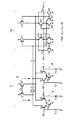
- FIG. 1 is a circuit diagram of the comparator 1 according to the first embodiment.
- the comparator 1 of FIG. 1 is used in, for example, a sequential comparison type ADC, but the application of the comparator 1 of FIG. 1 is not necessarily limited to the ADC.
- Two differential input signal pairs (hereinafter, referred to as a first differential input signal pair and a second differential input signal pair) Vin_p, Vin_n, Vns_p, and Vns_n are input to the comparator 1 of FIG.
- the comparator 1 outputs the differential output signal pairs Vout_p and Vout_n corresponding to the difference signal of the first differential input signal pair Vin_p and Vin_n and the difference signal of the second differential input signal pair Vns_p and Vns_n.
- the comparator 1 of FIG. 1 is a dynamic comparator 1 that performs a comparison operation of two differential input signal pairs Vin_p, Vin_n, Vns_p, and Vns_n.
- the first comparison circuit 2 includes the difference signal between the first differential input signal pair Vin_p and Vin_n generated by connecting the first input terminal TL1 to the positive side and the second input terminal TL2 to the negative side. Outputs a signal corresponding to the difference signal between the second differential input signal pair Vns_p and Vns_n generated by connecting the third input terminal TL3 to the positive side and connecting the fourth input terminal TL4 to the negative side. ..
- the second comparison circuit 3 includes the difference signal between the first differential input signal pair Vin_p and Vin_n generated by connecting the first input terminal TL1 to the negative side and the second input terminal TL2 to the positive side. Outputs a signal corresponding to the difference signal between the second differential input signal pair Vns_p and Vns_n generated by connecting the third input terminal TL3 to the positive side and connecting the fourth input terminal TL4 to the negative side. ..
- the first comparison circuit 2 and the second comparison circuit 3 have a common circuit configuration and common electrical characteristics. More specifically, the corresponding transistors in the first comparison circuit 2 and the second comparison circuit 3 have a common gate width and gate length.
- the first comparison circuit 2 responds to the difference signal between the first differential input signal pair Vin_p and Vin_n generated by connecting the first input terminal TL1 to the positive side and the second input terminal TL2 to the negative side.
- the first differential output signal pair is output from the first output node n1 and the second output node n2.
- the voltage fluctuation amount of the third input terminal TL3 generated in response to the voltage fluctuation of the first output node n1 is equal to the voltage fluctuation amount of the fourth input terminal TL4 generated in response to the voltage fluctuation of the second output node n2.
- the second comparison circuit 3 does not directly participate in the comparison operation of the comparator 1, but acts as a dummy circuit.
- the first comparator circuit 2 has a first comparator 4 and a second comparator 5.
- the first comparator 4 responds to the difference signal between the first differential input signal pair Vin_p and Vin_n generated by connecting the first input terminal TL1 to the positive side and the second input terminal TL2 to the negative side.
- the first differential output signal pair is output from the first output node n1 and the second output node n2.
- the third input terminal TL3 is connected to the positive side and the fourth input terminal TL4 is connected to the negative side, and the second comparator 5 responds to the difference signal of the second differential input signal pair generated.
- the differential output signal pair is output from the first output node n1 and the second output node n2.
- the first comparator 4 has N-type MOS transistors Q1 and Q2.
- the first differential input signal Vin_p is input to the gate of the transistor Q1.
- the gate of transistor Q1 is on the positive side.
- the first differential input signal Vin_n is input to the gate of the transistor Q2.
- the gate of transistor Q2 is on the negative side.
- An N-type MOS transistor Q3 is connected between each source of the transistors Q1 and Q2 and the ground node.
- a clock signal Clk is input to the gate of the transistor Q3.
- the transistors Q1 and Q2 perform a comparison operation between the first differential input signal vs. Vin_p and Vin_n, and when the clock signal Clk is at a low level, the comparison operation is stopped.
- the drain of the transistor Q1 is connected to the first output node n1, and the drain of the transistor Q2 is connected to the second output node n2.
- the second comparator 5 has N-type MOS transistors Q4 and Q5.
- the first differential input signal Vns_p is input to the gate of the transistor Q4.
- the gate of Transis Q4 is on the positive side.
- the second differential input signal Vns_n is input to the gate of the transistor Q5.
- the gate of transistor Q5 is on the negative side.
- An N-type MOS transistor Q6 is connected between the source of the transistors Q4 and Q5 and the ground node.
- a clock signal Clk is input to the gate of the transistor Q6.
- the transistors Q1 and Q2 perform a comparison operation between the first differential input signal vs. Vin_p and Vin_n, and when the clock signal Clk is at a low level, the comparison operation is stopped.
- Each drain of the transistors Q4 and Q5 is connected to the first output node n1 and the second output node n2.
- a pull-up circuit (first voltage setting circuit) 6 is connected to the first output node n1 and the second output node n2.
- the pull-up circuit 6 pulls up the first output node n1 and the second output node n2 to a high level when the clock signal Clk is at a low level, that is, within a period during which the first comparison circuit 2 does not perform the comparison operation.
- the pull-up circuit 6 has a P-type MOS transistor Q7 connected to the first output node n1 and a P-type MOS transistor Q8 connected to the second output node n2.
- a clock signal Clk is input to the gates of the transistors Q7 and Q8.
- the second comparator circuit 3 has a third comparator 7 and a fourth comparator 8.
- the third comparator 7 responds to the difference signal between the first differential input signal pair Vin_p and Vin_n generated by connecting the second input terminal TL2 to the positive side and connecting the first input terminal TL1 to the negative side.
- the third differential output signal pair is output from the first internal node n3 and the second internal node n4.
- the third input terminal TL3 is connected to the positive side and the fourth input terminal TL4 is connected to the negative side to generate a fourth differential input signal pair according to the difference signal.
- the differential output signal pair is output from the first internal node n3 and the second internal node n4.
- the third comparator 7 has N-type MOS transistors Q9 and Q10.
- the first differential input signal Vin_n is input to the gate of the transistor Q9.
- the gate of transistor Q9 is on the positive side.
- the first differential input signal Vin_p is input to the gate of the transistor Q10.
- the gate of transistor Q10 is on the negative side.
- An N-type MOS transistor Q11 is connected between the source of the transistors Q9 and Q10 and the ground node.
- a clock signal Clk is input to the gate of the transistor Q11.
- the transistors Q9 and Q10 perform a comparison operation between the first differential input signal vs. Vin_p and Vin_n, and when the clock signal Clk is at a low level, the comparison operation is stopped.
- the drain of the transistor Q9 is connected to the first internal node n3, and the drain of the transistor Q10 is connected to the second internal node n4.
- the fourth comparator 8 has N-type MOS transistors Q12 and Q13.
- the second differential input signal Vns_p is input to the gate of the transistor Q12.
- the gate of transistor Q12 is on the positive side.
- the second differential input signal Vns_n is input to the gate of the transistor Q13.
- the gate of transistor Q13 is on the negative side.
- An N-type MOS transistor Q14 is connected between the source of the transistors Q12 and Q13 and the ground node.
- a clock signal Clk is input to the gate of the transistor Q14.
- the transistors Q12 and Q13 perform a comparison operation between the first differential input signal vs. Vin_p and Vin_n, and when the clock signal Clk is at a low level, the comparison operation is stopped.
- the drains of the transistors Q12 and Q13 are connected to the first internal node n3 and the second internal node n4.
- a pull-up circuit 9 (second voltage setting circuit) is connected to the first internal node n3 and the second internal node n4.
- the pull-up circuit 9 pulls up the first internal node n3 and the second internal node n4 to a high level when the clock signal Clk is at a low level.
- the pull-up circuit 9 has a P-type MOS transistor Q15 connected to the first internal node n3 and a P-type MOS transistor Q16 connected to the second internal node n4.
- a clock signal Clk is input to the gates of the transistors Q15 and Q16.
- the first internal node n3 and the second internal node n4 of the second comparison circuit 3 acting as a dummy circuit are not connected to anything other than the dummy circuit.
- the first output node n1 and the second output node n2 of the first comparison circuit 2 are connected to the latch circuit 10.
- the latch circuit 10 holds a signal indicating the comparison result output from the first comparison circuit 2 at the timing when the clock signal Clk transitions from the high level to the low level.
- the latch circuit 10 has P-type MOS transistors Q17 to Q20 and N-type MOS transistors Q21 to Q26.
- the first output node n1 is connected to each gate of the transistors Q17, Q21 and Q22.
- the second output node n2 is connected to each gate of the transistors Q18, Q24 and Q25.
- the gates of the transistors Q20 and Q26 and the drains of the transistors Q19 and Q23 are connected to the output terminal TL5 that outputs the differential output voltage Vout_p of the comparator 1.
- the gates of the transistors Q19 and Q23 and the drains of the transistors Q25 and Q26 are connected to the output terminal TL6 that outputs the differential output voltage Vout_n of the comparator 1.
- Comparator 1 in FIG. 1 starts a comparison operation when the clock signal Clk transitions from a low level to a high level. While the clock signal Clk is low level, the first output node n1 and the second output node n2 are pulled up to the power supply voltage level. When the clock signal Clk transitions to a high level, the voltage levels of the first output node n1 and the second output node n2 decrease as the transistors Q1, Q2, Q4, and Q5 are turned on. When Vin_p + Vns_p> Vin_n + Vns_n, the discharge rate of Vgm_p> the discharge rate of Vgm_n. On the contrary, when Vin_p + Vns_p ⁇ Vin_n + Vns_n, the discharge rate of Vgm_p is less than the discharge rate of Vgm_n.
- FIG. 2A and 2B are waveform diagrams of Vgm_p and Vgm_n during the comparative operation of the comparator 1.
- FIG. 2A is a waveform diagram when Vin_p + Vns_p> Vin_n + Vns_n
- FIG. 2B is a waveform diagram when Vin_p + Vns_p ⁇ Vin_n + Vns_n.
- the first differential input signal pair Vin_p, the signal Vin_p on the positive phase side of Vin_n is connected to the gate of the transistor Q1 on the positive phase side of the first comparator 4 in the first comparison circuit 2. At the same time, it is connected to the gate of the transistor Q10 on the negative phase side of the third comparator 7 in the second comparator circuit 3. Further, the signals Vin_n on the negative phase side of the first differential input signal pair Vin_p and Vin_n are connected to the gate of the transistor Q2 on the negative phase side of the first comparator 4 in the first comparator circuit 2, and the second comparison is performed. It is connected to the gate of the transistor Q9 on the positive phase side of the fourth comparator 8 in the circuit 3. In this way, in the first comparison circuit 2 and the second comparison circuit 3, the connection destinations of the first differential input signal pair Vin_p and Vin_n are reversed.
- the voltage level of the first output node n1 and the second output node n2 from which the comparison result of the first comparison circuit 2 is output varies greatly depending on the comparison result of the first comparison circuit 2.
- the transistors Q1 or Q2 in FIG. 1 are turned on, the voltage level of the first output node n1 or the second output node n2 is lowered by discharge.
- the transistor Q1 or Q2 of the transistor Q1 or Q2 passes through the parasitic capacitance of the MOS of the transistor Q1 or Q2 in the first comparison circuit 2.
- a so-called kickback current in which a current flows through the gate, may occur.
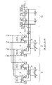
- FIG. 3 is a circuit diagram of a sequential comparison type ADC 11 provided with the comparator 1 of FIG.
- the sequential comparison type ADC 11 of FIG. 3 shows an example of converting a differential input signal pair into a 5-bit digital signal.
- the number of bits of the sequential comparison type ADC 11 is arbitrary. Further, the circuit configuration of the sequential comparison type ADC 11 is not limited to that shown in FIG.
- the sequential comparison type ADC 11 of FIG. 3 includes a first sampling switch 12, a second sampling switch 13, a first digital-analog converter (hereinafter, first DAC) 14, and a second digital-analog converter (second DAC 15).
- a filter circuit 16, a comparator 1, and a control circuit (SAR logic) 17 are provided.
- the first DAC14 and the second DAC15 are collectively referred to as a capacitance DAC18.
- the first sampling switch 12 switches whether or not to sample one of the differential input signal vs. Vad_p and Vad_n signals, Vad_p.
- the second sampling switch 13 switches whether or not to sample the other signal Vad_n of the differential input signal pair Vad_p and Vad_n.
- the first DAC 14 converts one of the sampled signals Vad_p into a digital signal consisting of a plurality of bits in order bit by bit, and outputs a signal of a voltage level corresponding to the unconverted bits.
- the first DAC 14 has five capacitors C1 to C5 having different capacities by a power of two, and three switches (first to third switches) SW1 to SW3 connected to the capacitors C1 to C5.
- the first switch SW1 switches whether or not one end of the capacitor is set to 0V.
- the second switch SW2 switches whether or not one end of the capacitor is set to the common voltage Vcom.
- the third switch SW3 switches whether or not one end of the capacitor is set to the reference voltage Vref.
- the common voltage Vcom is, for example, a voltage level of 1/2 of the reference voltage Vref.
- the first to third switches SW1 to SW3 are switched on or off based on the control signal from the control circuit 17.
- the control circuit 17 turns on the second switch SW2 at the start of the comparison operation. After that, the control circuit 17 turns on the first switch SW1 when it wants to lower the output node voltage Vin_p of the first DAC 14, and turns on the third switch SW3 when it wants to raise the output node voltage Vin_p of the first DAC 14.
- the second DAC 15 sequentially converts the other sampled signal into a digital signal composed of a plurality of bits one bit at a time, and outputs a signal with a voltage level corresponding to the unconverted bits.
- the second DAC 15 is configured in the same manner as the first DAC 14, and switches the first to third switches SW1 to SW3 based on the control signal from the control circuit 17 in the same manner as the first DAC 14.
- the filter circuit 16 samples and outputs the output signal of the first DAC 14 and the output signal of the second DAC 15.
- Comparator 1 has the configuration shown in FIG.
- the comparator 1 has a first differential input signal pair Vin_p, Vin_n that pairs an output signal of the first DAC 14 and an output signal of the second DAC 15, and a second differential input signal pair Vns_p, Vns_n output from the filter circuit 16. Is entered.
- the comparator 1 outputs a signal corresponding to the difference signal between the first differential input signal vs. Vin_p and Vin_n and the difference signal between the second differential input signal vs. Vns_p and Vns_n.
- the control circuit 17 performs switching control of the first to third switches SW1 to SW3 in the first DAC14 and the second DAC15 based on the output signal of the comparator 1.
- FIG. 4 is a voltage waveform diagram of the output node voltage Vin_p of the first DAC 14 and the output node voltage Vin_n of the second DAC 15 of FIG.
- both the first sampling switch 12 and the second sampling switch 13 are turned on to sample the differential input signal pairs Vad_p and Vad_n.
- one end of each of the capacitors C1 to C5 is set to the common voltage Vcom via the second switch SW2.
- the electric charge corresponding to the difference signal between the differential input signal vs. Vad_p and Vad_n is accumulated in the capacitance DAC18.
- the output signal of the first DAC 14 and the output signal of the second DAC 15 constituting the capacitance DAC 18 are the first differential input signal pair Vin_p and Vin_n input to the comparator 1.
- the differential output signal of the filter circuit 16 is the second differential input signal pair Vns_p and Vns_n input to the comparator 1.
- both the first sampling switch 12 and the second sampling switch 13 are turned off, and the comparison operation by the comparator 1 is started.
- the output of the capacitance DAC 18 is controlled so that the output voltage becomes smaller in order from the above bits according to the sampled differential input signal vs. the difference signal of Vad_p and Vad_n, and the output voltage gradually approaches zero.
- the voltage remaining in the capacitance DAC 18 is sampled by the filter circuit 16 to change the output voltage of the filter circuit 16.
- the residual voltage at the completion of control of the capacitance DAC 18 is a very small voltage level, and the filter circuit 16 continues to output a signal with a small voltage level. That is, the state of the difference signal (Vns_p ⁇ Vns_n) ⁇ 0 between the second differential input signal vs. Vns_p and Vns_n is maintained. Therefore, when the comparator 1 of FIG. 1 is used in the ADC 11 of FIG. 3, the difference between the discharge rates of the voltage Vgm_p of the first output node n1 of FIG. 1 and the voltage Vgm_n of the second output node n2 is the first differential input signal. It is almost determined only by the difference signal between Vin_p and Vin_n.
- the comparator 1 of FIG. 1 when the voltage Vgm_p of the first output node n1 and the voltage Vgm_n of the second output node n2 are discharged, the gates of the transistors Q1 and Q2 in the first comparator 4 and the second A kickback current flows through the gates of transistors Q4 and Q5 in the comparator 5.
- the waveform of the kickback current changes greatly depending on the discharge rate of the voltage Vgm_p of the first output node n1 and the voltage Vgm_n of the second output node n2.
- the first differential input signal pairs Vin_p and Vin_n input to the comparator 1 are connected to the output node of the capacitance DAC18, and there are a plurality of capacitors C1 to C5 in the capacitance DAC18. Even if a kickback current flows through the gates of the transistors Q1 and Q2 in the first comparator 4 of No. 1, the voltage fluctuations of the first differential input signal pair Vin_p and Vin_n are not large. On the other hand, since the output node of the filter circuit 16 to which the second differential input signal pair Vns_p and Vns_s are connected does not have a large capacitor, it kicks to the gate of the transistors Q4 and Q5 in the second comparator 5 of FIG. When the back current flows, the voltage fluctuations of the second differential input signal vs. Vns_p and Vns_s may become relatively large due to the influence.
- the discharge of the differential output voltages vs. Vgm_p and Vgm_n of the first and second output nodes n1 and n2 causes a kickback to the second differential input signals vs. Vns_p and Vns_n.
- Vin_p Vin_n
- Vns_p and Vns_n are the same, and the difference signal (Vns_p-Vns_n) of the second differential input signal vs. Vns_p and Vns_n does not fluctuate.
- Vin_p Vin_n
- the discharge rate is different, and the kickback current waveforms for the second differential input signal vs. Vns_p and Vns_n are also different. Therefore, it appears as a change in the difference signal (Vns_p-Vns_n) between the second differential input signal vs. Vns_p and Vns_n.
- Vin_p and Vin_n the larger the difference in discharge rate. Also becomes large, and the change of the difference signal (Vns_p-Vns_n) between the second differential input signal vs. Vns_p and Vns_n becomes large.
- the output signal level of the filter circuit 16 is essentially a small voltage level. If there is a voltage fluctuation in the output signal level of the filter circuit 16 due to kickback, there is a risk that the ADC 11 will not operate as desired, and the characteristics of the ADC 11 itself will be deteriorated. Further, if the output impedance of the filter circuit 16 is lowered in order to reduce the voltage fluctuation, the design of the filter circuit 16 itself becomes difficult, such as an increase in current consumption.
- the connection destinations of the first differential input signal pair Vin_p and Vin_n are reversed.
- the voltage fluctuation due to the kickback of one signal Vns_p of the second differential input signal vs. Vns_p and Vns_n and the voltage fluctuation due to the kickback of the other signal Vns_n of the second differential input signal vs. Vns_p and Vns_n. Can be made equal, and the voltage fluctuation due to kickback of each gate of the transistors Q4 and Q5 in the second comparator 5 can be offset. This will be described in more detail.
- the kickback current from the voltage Vgm_p of the first output node n1 to the second differential input signal Vns_p is I ⁇
- the kickback current from the voltage Vgm_n of the second output node n2 to the second differential input signal Vns_n is I ⁇
- the difference between the kickback currents of the second differential input signal pair Vns_p and Vns_n when the second comparator circuit 3 which is a dummy circuit does not exist is I ⁇ -I ⁇ .
- the discharge rate of the second internal node n4 voltage Vgm_dmy_n in the second comparison circuit 3 which is a dummy circuit is the same as the discharge rate of the first internal node n3 voltage Vgm_dmy_p. Therefore, the kickback current from the second internal node n4 voltage Vgm_dmy_n to the second differential input signal Vns_n is I ⁇ . Similarly, the kickback current from the first internal node n3 voltage Vgm_dmy_p to the second differential input signal Vns_p is I ⁇ .
- the kickback current to the second differential input signal Vns_p is I ⁇ + I ⁇
- the fact that the difference in kickback current is zero means that fluctuations due to kickback of the second differential input signals Vns_p and Vns_n of the comparator 1 are eliminated.
- the first comparator 4 in the first comparison circuit 2 and the third comparator 7 in the second comparison circuit 3 have the first differential input signal pair Vin_p and Vin_n. Since the connection destinations of the positive phase side and negative phase side signals are reversed from each other, the discharge of the first output node n1 and the second output node n2 kicks back to the gates of the transistors Q4 and Q5 in the second comparator 5. Even if a current flows, the kickback current flowing through the gates of the transistors Q4 and Q5 can be made equal, so that the voltage fluctuations due to the kickback current cancel each other out, and the first output node n1 and the second output node n2 kickback. It is no longer affected by electric current.
- FIG. 5 is a circuit diagram of the comparator 100 according to a comparative example.
- the comparator 100 of FIG. 5 includes the first comparison circuit 2 and the latch circuit 10 of FIG. 1, but does not have the second comparison circuit 3.
- the kickback current from the voltage Vgm_p of the first output node n1 to the second differential input signal Vns_p is I ⁇
- the kickback current from the voltage Vgm_n of the second output node n2 to the second differential input signal Vns_n is I ⁇
- the difference in kickback current between the gates of the transistors Q4 and Q5 in the second comparator 5 is I ⁇ -I ⁇ because the second comparator circuit 3 which is a dummy circuit does not exist, and is zero. It does not become. Therefore, in the comparator 100 of FIG. 5, when the voltage levels of the voltage Vgm_p of the first output node n1 and the voltage Vgm_n of the second output node n2 fluctuate depending on the discharge rate, the difference in kickback current (I ⁇ -) according to the fluctuations. I ⁇ ) occurs, and the differential output voltages Vgm_p and Vgm_n of the comparator 100 fluctuate according to the difference.
- FIG. 6A is a signal waveform diagram of each part in the comparator 1 of FIG. 1 by simulation
- FIG. 6B is a signal waveform diagram of each part in the comparator 100 of FIG. 5 by simulation.
- 6A and 6B show the voltage waveform of the clock signal Clk, the voltage waveform of the first differential input signal pair Vin_p, Vin_n difference signal (Vin_p-Vin_n), and the second differential input signal pair Vns_p, Vns_n.
- the voltage waveform of the difference signal (Vns_p-Vns_n) is shown in the figure.
- the comparators 1 and 100 start the comparison operation at time t1.
- the control circuit 17 determines the charge charge of the capacitor of the capacitance DAC 18 in order from the upper side so that the output voltage (Vin_p-Vin_n) of the capacitance DAC 18 becomes zero.
- the output signal (Vns_p-Vns_n) of the filter circuit 16 is approximately 0 V in FIG. 6A, whereas in FIG. 6B, a large spike-like voltage fluctuation occurs every time the comparator 100 performs a comparison operation. More specifically, in the simulation result of FIG. 6A, the output voltage of the filter circuit 16 is a minute DC voltage of about 300 ⁇ V, whereas in FIG. 6B, a very large spike-like voltage fluctuation occurs. It may exceed 1 mV at the maximum.
- the output voltage of the filter circuit 16 is kept constant during the comparison operation. If the output voltage of the filter circuit 16 fluctuates, the analog-to-digital conversion operation may not be performed normally, and the characteristics of the ADC 11 itself are deteriorated.
- the comparator 1 is different from the first comparison circuit 2 in which the first differential input signal pair Vin_p, Vin_n and the second differential input signal pair Vns_p, Vns_n are input.
- a second comparison circuit 3 which is a dummy circuit having the same circuit configuration and the same electrical characteristics as the first comparison circuit 2, is provided.
- the first differential input signal pair Vin_p and Vin_n are provided. Reverse the connection destinations. More specifically, in the first comparator 4 in the first comparator circuit 2, the signals on the positive phase side of the first differential input signal pair Vin_p and Vin_n are input to the gate of the transistor on the positive phase side.
- the signals on the positive phase side of the first differential input signal pair Vin_p and Vin_n are input to the gate of the transistor on the negative phase side.
- a kickback current flows through the gates of the transistors Q4 and Q5 in the second comparator 5 due to the voltage fluctuations of the voltages Vgm_p and Vgm_n of the first output node n1 and the second output node n2 of the first comparator circuit 2.
- the voltage fluctuations due to the kickback current at the gates of the transistors Q4 and Q5 can be made equal.
- the voltages Vgm_p and Vgm_n of the first output node n1 and the second output node n2 do not cause voltage fluctuation due to the kickback current, the output voltage of the comparator 1 can be stabilized, and the performance deterioration of the ADC 11 can be suppressed.
- the first comparator 4 and the second comparator 5 in the first comparison circuit 2 and the third comparator 7 and the fourth comparator 8 in the second comparison circuit 3 are N-type MOS transistors. However, it may be composed of a P-type MOS transistor.
- FIG. 7 is a circuit diagram of the comparator 1a according to the second embodiment.
- the comparator 1a of FIG. 7 is obtained by reversing the conductive type of each transistor in the comparator 1 of FIG. 1, and has transistors Q31 to Q38, Q41 to Q46, and Q51 to Q56.
- the first comparator 4 and the second comparator 5 in the first comparison circuit 2 in the comparator 1a of FIG. 7 are composed of P-type MOS transistors Q31 to Q36.
- the pull-up circuit 6 is composed of N-type MOS transistors Q37 and Q38.
- the conductive type of each transistor Q51 to Q56 in the latch circuit 10 is also opposite to that of the latch circuit 10 of FIG.
- the comparator 1a of FIG. 7 similarly to the comparator 1 of FIG. 1, in the first comparator 4 in the first comparison circuit 2 and the third comparator 7 in the second comparison circuit 3, the first differential input signal.
- the connection destinations of the positive side signal and the negative side signal of Vin_p and Vin_n are opposite to each other. Therefore, also in the comparator 1a of FIG. 7, similarly to the comparator 1 of FIG. 1, the transistors Q4 in the second comparator 5 are caused by the voltage fluctuations of the voltages Vgm_p and Vgm_n of the first output node n1 and the second output node n2. Even if a kickback current flows through the gate of Q5, the voltages Vgm_p and Vgm_n do not fluctuate due to the kickback current, and the performance deterioration of the ADC 11 can be suppressed.
- the third embodiment has a different configuration of the latch circuit 10 from the first embodiment.
- FIG. 8 is a circuit diagram of the comparator 1b according to the third embodiment.
- the comparator 1b of FIG. 8 includes a first comparison circuit 2 and a second comparison circuit 3 having the same circuit configuration as the comparator 1 of FIG.
- the comparator 1b of FIG. 8 includes a first latch circuit 21 connected to a first output node n1 and a second output node n2 of the first comparison circuit 2, and a first internal node n3 and a second internal of the second comparison circuit 3. It includes a second latch circuit 22 connected to the node n4.
- the first latch circuit 21 has P-type MOS transistors Q61 to Q64 and N-type MOS transistors Q65 and Q66.
- a clock signal Clk is input to each gate of the transistors Q61 and Q63.
- the gates of the transistors Q62 and Q65 and the drains of the transistors Q63 and Q64 are connected to the output node voltage Vout_p.
- the gates of the transistors Q64 and Q66 and the drains of the transistors Q62 and Q65 are connected to the output node voltage Vout_n.
- the source of the transistor Q65 is connected to the voltage Vgm_p of the first output node n1
- the source of the transistor Q66 is connected to the voltage Vgm_n of the second output node n2.
- the second latch circuit 22 has P-type MOS transistors Q71 to Q74 and N-type MOS transistors Q75 and Q76, and is configured in the same manner as the first latch circuit 21.
- the comparator 1b in FIG. 8 starts the comparison operation. After that, when the clock signal Clk transitions from the high level to the low level, the first latch circuit 21 holds the comparison result by the first comparison circuit 2, and the second latch circuit 22 holds the comparison result by the second comparison circuit 3. Hold.
- the comparator 1b of FIG. 8 is a first differential input signal in the first comparator 4 in the first comparison circuit 2 and the third comparator 7 in the second comparison circuit 3.
- the connection destinations of the positive side signal and the negative side signal of Vin_p and Vin_n are opposite to each other. Therefore, also in the comparator 1b of FIG. 8, similarly to the comparator 1 of FIG. 1, the transistors Q4 in the second comparator 5 are caused by the voltage fluctuations of the voltages Vgm_p and Vgm_n of the first output node n1 and the second output node n2. Even if a kickback current flows through the gate of Q5, the voltages Vgm_p and Vgm_n do not fluctuate due to the kickback current, and the performance deterioration of the ADC 11 can be suppressed.
- the comparator 1c according to the fourth embodiment is for inputting the signal output from the first comparison circuit 2 to the latch circuit 10 after waveform shaping.
- FIG. 9 is a circuit diagram of the comparator 1c according to the fourth embodiment.
- the comparator 1c of FIG. 9 includes a first comparison circuit 2, a second comparison circuit 3, and a latch circuit 10 having the same configuration as the comparator 1 of FIG.
- the comparator 1c of FIG. 9 includes inverters 23 and 24.
- the inverters 23 and 24 are connected to the first output node n1 and the second output node n2 connected to the first comparison circuit 2, respectively.
- the inverters 23 and 24 invert the logic of the input signal and output it. At that time, the inverters 23 and 24 perform waveform shaping to make the output signal waveform steep. In this way, the inverters 23 and 24 operate as a waveform shaping circuit.
- various logical operation elements for example, NAND element, NOR element, etc. may be used.
- the voltage levels of the voltages Vgm_p and Vgm_n of the first output node n1 and the second output node n2 decrease due to the discharge by the transistors Q1, Q2, Q4, and Q5 in the first comparator 4 and the second comparator 5.
- the inverters 23 and 24 are charged as the voltages Vgm_p and Vgm_n of the first output node n1 and the second output node n2 are discharged.
- the latch circuit 10 performs a holding operation according to the logic according to the difference in charging speed between the output voltages of the inverters 23 and 24.
- the comparator 1c of FIG. 9 is a first differential input signal in the first comparator 4 in the first comparison circuit 2 and the third comparator 7 in the second comparison circuit 3.
- the connection destinations of the positive side signal and the negative side signal of Vin_p and Vin_n are opposite to each other. Therefore, also in the comparator 1b of FIG. 8, similarly to the comparator 1 of FIG. 1, the transistors Q4 in the second comparator 5 are caused by the voltage fluctuations of the voltages Vgm_p and Vgm_n of the first output node n1 and the second output node n2. Even if a kickback current flows through the gate of Q5, the voltages Vgm_p and Vgm_n do not fluctuate due to the kickback current, and the performance deterioration of the ADC 11 can be suppressed.
- the waveform shaping circuit by the inverters 23, 24 and the like of FIG. 9 may be provided in the comparators 1a and 1b of FIG. 7 or FIG.
- the output signal of the first comparator circuit 2 is once waveform-shaped by the inverters 23, 24 and the like, and then the latch circuit 10 performs the holding operation. Therefore, the latch circuit 10 quickly performs the holding operation.
- the operation speed of the comparator 1c shown in FIG. 9 can be improved.
- the technical features common to the comparators 1, 1a, 1b, and 1c according to the first to fourth embodiments described above are that the second comparison circuit 3 having the same circuit configuration and the same electrical characteristics as the first comparison circuit 2 is provided.
- the connection destinations of the first differential input signal pair Vin_p and Vin_n are reversed.
- fluctuations in the voltages Vgm_p and Vgm_n of the first output node n1 and the second output node n2 of the first comparison circuit 2 due to the kickback current can be suppressed.
- the present technology can have the following configurations. (1) The first input terminal and the second input terminal to which the first differential input signal pair is input, and The third input terminal and the fourth input terminal to which the second differential input signal pair is input, and The difference signal of the first differential input signal pair generated by connecting the first input terminal to the positive side and connecting the second input terminal to the negative side, and the third input terminal to the positive side.
- a first comparison circuit that outputs a signal corresponding to the difference signal of the second differential input signal pair generated by connecting and connecting the fourth input terminal to the negative side. The difference signal of the first differential input signal pair generated by connecting the first input terminal to the negative side and connecting the second input terminal to the positive side, and the third input terminal to the positive side.
- the comparator according to (1) comprising a first output terminal and a second output terminal for outputting a differential output signal pair corresponding to the signal output from the first comparison circuit.
- the comparator according to (1) or (2) wherein the voltage level of the difference signal of the first differential input signal pair is larger than the voltage level of the difference signal of the second differential input signal pair.
- the first comparison circuit is a first output node that differentially outputs a signal corresponding to the difference signal of the first differential input signal pair and the difference signal of the second differential input signal pair. And has a second output node
- the voltage fluctuation amount of the third input terminal generated in response to the voltage fluctuation of the first output node is equal to the voltage fluctuation amount of the fourth input terminal generated in response to the voltage fluctuation of the second output node, (1).
- the comparator according to any one of (4) to (4).
- the first comparison circuit is A first differential output signal pair corresponding to the difference signal of the first differential input signal pair generated by connecting the first input terminal to the positive side and connecting the second input terminal to the negative side.
- the first comparator that outputs to the first output node and the second output node, and A second differential output signal pair corresponding to the difference signal of the second differential input signal pair generated by connecting the third input terminal to the positive side and connecting the fourth input terminal to the negative side is provided. It has a first output node and a second comparator that outputs from the second output node.
- the second comparison circuit is A third differential output signal pair corresponding to the difference signal of the first differential input signal pair generated by connecting the second input terminal to the positive side and connecting the first input terminal to the negative side is provided.
- a third comparator that outputs to the first internal node and the second internal node, A fourth differential output signal pair corresponding to the difference signal of the second differential input signal pair generated by connecting the third input terminal to the positive side and connecting the fourth input terminal to the negative side is provided.
- the comparator according to (5) further comprising a first internal node and a fourth comparator that outputs from the second internal node.
- a first voltage setting circuit that sets the first output node and the second output node to a predetermined voltage level within a period in which the first comparison circuit does not perform a comparison operation.
- the second voltage setting circuit is provided, wherein the first internal node and the second internal node are set to a predetermined voltage level within a period in which the second comparison circuit does not perform the comparison operation, according to (6).
- comparator Each of the first comparator, the second comparator, the third comparator, and the fourth comparator has an N-type transistor.
- Each of the first comparator, the second comparator, the third comparator, and the fourth comparator has a P-type transistor.
- the comparator according to (7), wherein each of the first voltage setting circuit and the second voltage setting circuit has an N-type transistor.
- the first comparator, the second comparator, the third comparator, and the fourth comparator perform a comparison operation when the predetermined signal is the first logic, and the predetermined signal is generated. In the case of the second logic, the comparison operation is stopped and the comparison operation is stopped.
- the first voltage setting circuit sets the first output node and the second output node to the predetermined voltage level when the predetermined signal is the second logic.
- the second voltage setting circuit sets the first internal node and the second internal node to the predetermined voltage level when the predetermined signal is the second logic, according to (7) to (9).
- the comparator according to any one item.
- a first sampling switch that switches whether to sample one signal of the differential input signal pair, and A first digital-to-analog converter that converts one of the sampled signals into a digital signal consisting of a plurality of bits in order bit by bit and outputs a signal with a voltage level corresponding to the unconverted bits.
- a second sampling switch that switches whether to sample the other signal of the differential input signal pair, and A second digital-to-analog converter that converts the other sampled signal into a digital signal consisting of a plurality of bits in order bit by bit and outputs a signal with a voltage level corresponding to the unconverted bits.
- a filter circuit that samples and outputs the output signal of the first digital-to-analog converter and the output signal of the second digital-to-analog converter.
- the difference signal of the first differential input signal pair that pairs the output signal of the first digital-analog converter and the output signal of the second digital-analog converter, and the second difference output from the filter circuit.
- a comparator that outputs the difference signal of the dynamic input signal pair and the corresponding signal, and The comparator includes a control circuit for controlling the first digital-to-analog converter and the second digital-to-analog converter based on the output signal of the comparator.
- a first comparison circuit that outputs a signal corresponding to the difference signal of the second differential input signal pair generated by connecting and connecting the fourth input terminal to the negative side.
Landscapes
- Engineering & Computer Science (AREA)
- Theoretical Computer Science (AREA)
- Manipulation Of Pulses (AREA)
- Analogue/Digital Conversion (AREA)
Abstract
[課題]キックバック電流を抑制して、比較結果を出力する信号にずれが生じないようにする。 [解決手段]コンパレータは、第1差動入力信号対が入力される第1入力端子及び第2入力端子と、第2差動入力信号対が入力される第3入力端子及び第4入力端子と、第1入力端子を正側に接続し、かつ第2入力端子を負側に接続して生成される第1差動入力信号対の差信号と、第3入力端子を正側に接続し、かつ第4入力端子を負側に接続して生成される第2差動入力信号対の差信号と、に応じた信号を出力する第1比較回路と、第1入力端子を負側に接続し、かつ第2入力端子を正側に接続して生成される第1差動入力信号対の差信号と、第3入力端子を正側に接続し、かつ第4入力端子を負側に接続して生成される第2差動入力信号対の差信号と、に応じた信号を出力する第2比較回路と、を備える。
Description
本開示は、コンパレータ及びアナログ-デジタル変換器に関する。
サンプリングスイッチと、2つの差動入力信号対が入力されるコンパレータと、デジタル-アナログ変換器(以下、DAC)とを備えた逐次比較型アナログ-デジタル変換器(以下、逐次比較型ADC)が知られている(非特許文献1参照)。この種のコンパレータは、一方の差動入力信号対の差信号と、他方の差動入力信号対の差信号とに応じた信号を保持する。コンパレータが保持した信号によりDACが制御され、DACの出力信号に基づいて2つの差動入力信号対が生成される。
"An Oversampling SAR ADC With DAC Mismatch Error Shaping Achieving 105 dB SFDR and 101 dB SNDR Over 1 kHz BW in 55 nm CMOS"(IEEE Journal of Solid-State Circuit, 2016)
しかしながら、これらの差動入力信号対の差信号の信号レベルが大きく変化すると、その変化の影響を受けて、差動入力信号対が入力されるトランジスタのゲートに電流(以下、キックバック電流と呼ぶ)が流れ、結果として差信号の信号レベルが変動するおそれがある。差信号の信号レベルが変動すると、コンパレータの出力信号にずれが生じ、ADCが正常に動作しなくなる。
そこで、本開示では、上述したキックバック電流を抑制して、比較結果を出力する信号にずれが生じないようにしたコンパレータ及びアナログ-デジタル変換器を提供するものである。
上記の課題を解決するために、本開示によれば、第1差動入力信号対が入力される第1入力端子及び第2入力端子と、
第2差動入力信号対が入力される第3入力端子及び第4入力端子と、
前記第1入力端子を正側に接続し、かつ前記第2入力端子を負側に接続して生成される前記第1差動入力信号対の差信号と、前記第3入力端子を正側に接続し、かつ前記第4入力端子を負側に接続して生成される前記第2差動入力信号対の差信号と、に応じた信号を出力する第1比較回路と、
前記第1入力端子を負側に接続し、かつ前記第2入力端子を正側に接続して生成される前記第1差動入力信号対の差信号と、前記第3入力端子を正側に接続し、かつ前記第4入力端子を負側に接続して生成される前記第2差動入力信号対の差信号と、に応じた信号を出力する第2比較回路と、を備える、コンパレータが提供される。
前記第1比較回路から出力された信号に応じた差動出力信号対を出力する第1出力端子及び第2出力端子を備えてもよい。
前記第1差動入力信号対の差信号の電圧レベルは、前記第2差動入力信号対の差信号の電圧レベルより大きくてもよい。
前記第1比較回路及び前記第2比較回路は、共通の回路構成及び共通の電気特性を有してもよい。
前記第1比較回路は、前記第1差動入力信号対の差信号と、前記第2差動入力信号対の差信号と、に応じた信号を差動で出力する第1出力ノード及び第2出力ノードを有し、
前記第1出力ノードの電圧変動に応じて生じる前記第3入力端子の電圧変動量は、前記第2出力ノードの電圧変動に応じて生じる前記第4入力端子の電圧変動量に等しくてもよい。
前記第1出力ノードの電圧変動に応じて生じる前記第3入力端子の電圧変動量は、前記第2出力ノードの電圧変動に応じて生じる前記第4入力端子の電圧変動量に等しくてもよい。
前記第1比較回路は、
前記第1入力端子を正側に接続し、かつ前記第2入力端子を負側に接続して生成される前記第1差動入力信号対の差信号に応じた第1差動出力信号対を前記第1出力ノード及び前記第2出力ノードに出力する第1比較器と、
前記第3入力端子を正側に接続し、かつ前記第4入力端子を負側に接続して生成される前記第2差動入力信号対の差信号に応じた第2差動出力信号対を前記第1出力ノード及び前記第2出力ノードから出力する第2比較器と、を有し、
前記第2比較回路は、
前記第2入力端子を正側に接続し、かつ前記第1入力端子を負側に接続して生成される前記第1差動入力信号対の差信号に応じた第3差動出力信号対を第1内部ノード及び第2内部ノードに出力する第3比較器と、
前記第3入力端子を正側に接続し、かつ前記第4入力端子を負側に接続して生成される前記第2差動入力信号対の差信号に応じた第4差動出力信号対を前記第1内部ノード及び前記第2内部ノードから出力する第4比較器と、を有してもよい。
前記第1比較回路が比較動作を行わない期間内に、前記第1出力ノード及び前記第2出力ノードを所定の電圧レベルに設定する第1電圧設定回路と、
前記第2比較回路が比較動作を行わない期間内に、前記第1内部ノード及び前記第2内部ノードを所定の電圧レベルに設定する第2電圧設定回路と、を備えてもよい。
前記第2比較回路が比較動作を行わない期間内に、前記第1内部ノード及び前記第2内部ノードを所定の電圧レベルに設定する第2電圧設定回路と、を備えてもよい。
前記第1比較器、前記第2比較器、前記第3比較器、及び前記第4比較器のそれぞれは、N型トランジスタを有し、
前記第1電圧設定回路及び前記第2電圧設定回路のそれぞれは、P型トランジスタを有してもよい。
前記第1電圧設定回路及び前記第2電圧設定回路のそれぞれは、P型トランジスタを有してもよい。
前記第1比較器、前記第2比較器、前記第3比較器、及び前記第4比較器のそれぞれは、P型トランジスタを有し、
前記第1電圧設定回路及び前記第2電圧設定回路のそれぞれは、N型トランジスタを有してもよい。
前記第1電圧設定回路及び前記第2電圧設定回路のそれぞれは、N型トランジスタを有してもよい。
前記第1比較器、前記第2比較器、前記第3比較器、及び前記第4比較器は、所定の信号が第1論理のときに比較動作を行うとともに、前記所定の信号が第2論理のときは比較動作を停止し、
前記第1電圧設定回路は、前記所定の信号が前記第2論理のときに、前記第1出力ノード及び前記第2出力ノードを前記所定の電圧レベルに設定し、
前記第2電圧設定回路は、前記所定の信号が前記第2論理のときに、前記第1内部ノード及び前記第2内部ノードを前記所定の電圧レベルに設定してもよい。
前記第1電圧設定回路は、前記所定の信号が前記第2論理のときに、前記第1出力ノード及び前記第2出力ノードを前記所定の電圧レベルに設定し、
前記第2電圧設定回路は、前記所定の信号が前記第2論理のときに、前記第1内部ノード及び前記第2内部ノードを前記所定の電圧レベルに設定してもよい。
前記第1比較回路から出力された信号を保持するラッチ回路を備えてもよい。
前記第1比較回路から出力された信号の波形整形を行う波形整形回路を備え、
前記ラッチ回路は、前記波形整形回路が波形整形した信号を保持してもよい。
前記ラッチ回路は、前記波形整形回路が波形整形した信号を保持してもよい。
前記波形整形回路は、インバータであってもよい。
前記第1比較回路から出力された信号を保持する第1ラッチ回路と、
前記第2比較回路から出力された信号を保持する第2ラッチ回路と、を備えてもよい。
前記第2比較回路から出力された信号を保持する第2ラッチ回路と、を備えてもよい。
本開示によれば、差動入力信号対の一方の信号をサンプリングするか否かを切り替える第1サンプリングスイッチと、
サンプリングされた前記一方の信号を複数ビットからなるデジタル信号に、1ビットずつ順に変換するとともに、未変換のビットに応じた電圧レベルの信号を出力する第1デジタル-アナログ変換器と、
前記差動入力信号対の他方の信号をサンプリングするか否かを切り替える第2サンプリングスイッチと、
サンプリングされた前記他方の信号を複数ビットからなるデジタル信号に、1ビットずつ順に変換するとともに、未変換のビットに応じた電圧レベルの信号を出力する第2デジタル-アナログ変換器と、
前記第1デジタル-アナログ変換器の出力信号と、前記第2デジタル-アナログ変換器の出力信号とをサンプリングして出力するフィルタ回路と、
前記第1デジタル-アナログ変換器の出力信号と前記第2デジタル-アナログ変換器の出力信号とを対とする第1差動入力信号対の差信号と、前記フィルタ回路から出力された第2差動入力信号対の差信号と、に応じた信号を出力するコンパレータと、
前記コンパレータの出力信号に基づいて、前記第1デジタル-アナログ変換器及び前記第2デジタル-アナログ変換器を制御する制御回路と、を備え
前記コンパレータは、
前記第1差動入力信号対が入力される第1入力端子及び第2入力端子と、
前記第2差動入力信号対が入力される第3入力端子及び第4入力端子と、
前記第1入力端子を正側に接続し、かつ前記第2入力端子を負側に接続して生成される前記第1差動入力信号対の差信号と、前記第3入力端子を正側に接続し、かつ前記第4入力端子を負側に接続して生成される前記第2差動入力信号対の差信号と、に応じた信号を出力する第1比較回路と、
前記第1入力端子を負側に接続し、かつ前記第2入力端子を正側に接続して生成される前記第1差動入力信号対の差信号と、前記第3入力端子を正側に接続し、かつ前記第4入力端子を負側に接続して生成される前記第2差動入力信号対の差信号と、に応じた信号を出力する第2比較回路と、を有する、アナログ-デジタル変換器が提供される。
以下、図面を参照して、コンパレータ及びアナログ-デジタル変換器の実施形態について説明する。以下では、コンパレータ及びアナログ-デジタル変換器の主要な構成部分を中心に説明するが、コンパレータ及びアナログ-デジタル変換器には、図示又は説明されていない構成部分や機能が存在しうる。以下の説明は、図示又は説明されていない構成部分や機能を除外するものではない。
(第1の実施形態)
図1は第1の実施形態によるコンパレータ1の回路図である。図1のコンパレータ1は、後述するように、例えば逐次比較型ADCで用いられるが、図1のコンパレータ1の用途は必ずしもADCには限らない。図1のコンパレータ1には、2つの差動入力信号対(以下、第1差動入力信号対と第2差動入力信号対と呼ぶ)Vin_p、Vin_n,Vns_p、Vns_nが入力される。コンパレータ1は、第1差動入力信号対Vin_p、Vin_nの差信号と、第2差動入力信号対Vns_p、Vns_nの差信号とに応じた差動出力信号対Vout_p、Vout_nを出力する。このように、図1のコンパレータ1は、2つの差動入力信号対Vin_p、Vin_n,Vns_p、Vns_nの比較動作を行うダイナミックコンパレータ1である。
図1は第1の実施形態によるコンパレータ1の回路図である。図1のコンパレータ1は、後述するように、例えば逐次比較型ADCで用いられるが、図1のコンパレータ1の用途は必ずしもADCには限らない。図1のコンパレータ1には、2つの差動入力信号対(以下、第1差動入力信号対と第2差動入力信号対と呼ぶ)Vin_p、Vin_n,Vns_p、Vns_nが入力される。コンパレータ1は、第1差動入力信号対Vin_p、Vin_nの差信号と、第2差動入力信号対Vns_p、Vns_nの差信号とに応じた差動出力信号対Vout_p、Vout_nを出力する。このように、図1のコンパレータ1は、2つの差動入力信号対Vin_p、Vin_n,Vns_p、Vns_nの比較動作を行うダイナミックコンパレータ1である。
図1のコンパレータ1は、第1差動入力信号対Vin_p、Vin_nが入力される第1入力端子TL1及び第2入力端子TL2と、第2差動入力信号対Vns_p、Vns_nが入力される第3入力端子TL3及び第4入力端子TL4と、第1比較回路2と、第2比較回路3と、を備えている。
第1比較回路2は、第1入力端子TL1を正側に接続し、かつ第2入力端子TL2を負側に接続して生成される第1差動入力信号対Vin_p、Vin_nの差信号と、第3入力端子TL3を正側に接続し、かつ第4入力端子TL4を負側に接続して生成される第2差動入力信号対Vns_p、Vns_nの差信号と、に応じた信号を出力する。
第2比較回路3は、第1入力端子TL1を負側に接続し、かつ第2入力端子TL2を正側に接続して生成される第1差動入力信号対Vin_p、Vin_nの差信号と、第3入力端子TL3を正側に接続し、かつ第4入力端子TL4を負側に接続して生成される第2差動入力信号対Vns_p、Vns_nの差信号と、に応じた信号を出力する。
第1比較回路2及び第2比較回路3は、共通の回路構成及び共通の電気特性を有する。より詳細には、第1比較回路2及び第2比較回路3内の対応するトランジスタ同士は、共通のゲート幅及びゲート長を有する。
第1比較回路2は、第1入力端子TL1を正側に接続し、かつ第2入力端子TL2を負側に接続して生成される第1差動入力信号対Vin_p、Vin_nの差信号に応じた第1差動出力信号対を第1出力ノードn1及び第2出力ノードn2から出力する。第1出力ノードn1の電圧変動に応じて生じる第3入力端子TL3の電圧変動量は、第2出力ノードn2の電圧変動に応じて生じる第4入力端子TL4の電圧変動量に等しい。これに対して、第2比較回路3は、コンパレータ1の比較動作には直接関与せず、ダミー回路として作用する。
第1比較回路2は、第1比較器4と第2比較器5を有する。
第1比較器4は、第1入力端子TL1を正側に接続し、かつ第2入力端子TL2を負側に接続して生成される第1差動入力信号対Vin_p、Vin_nの差信号に応じた第1差動出力信号対を第1出力ノードn1及び第2出力ノードn2から出力する。
第2比較器5は、第3入力端子TL3を正側に接続し、かつ第4入力端子TL4を負側に接続して生成される第2差動入力信号対の差信号に応じた第2差動出力信号対を第1出力ノードn1及び第2出力ノードn2から出力する。
第1比較器4は、N型MOSトランジスタQ1,Q2を有する。トランジスタQ1のゲートには、第1差動入力信号Vin_pが入力されている。トランジスタQ1のゲートが正側である。トランジスタQ2のゲートには、第1差動入力信号Vin_nが入力されている。トランジスタQ2のゲートが負側である。
トランジスタQ1,Q2の各ソースと接地ノードの間には、N型MOSトランジスタQ3が接続されている。トランジスタQ3のゲートには、クロック信号Clkが入力されている。クロック信号Clkがハイレベルのときに、トランジスタQ1,Q2は第1差動入力信号対Vin_p、Vin_nの比較動作を行い、クロック信号Clkがローレベルのときは比較動作を停止する。トランジスタQ1のドレインは第1出力ノードn1に接続され、トランジスタQ2のドレインは第2出力ノードn2に接続されている。
第2比較器5は、N型MOSトランジスタQ4,Q5を有する。トランジスタQ4のゲートには、第1差動入力信号Vns_pが入力されている。トランジスがQ4のゲートが正側である。トランジスタQ5のゲートには、第2差動入力信号Vns_nが入力されている。トランジスタQ5のゲートが負側である。
トランジスタQ4,Q5のソースと接地ノードの間には、N型MOSトランジスタQ6が接続されている。トランジスタQ6のゲートには、クロック信号Clkが入力されている。クロック信号Clkがハイレベルのときに、トランジスタQ1,Q2は第1差動入力信号対Vin_p、Vin_nの比較動作を行い、クロック信号Clkがローレベルのときは比較動作を停止する。トランジスタQ4,Q5の各ドレインは、第1出力ノードn1と第2出力ノードn2に接続されている。
第1出力ノードn1及び第2出力ノードn2には、プルアップ回路(第1電圧設定回路)6が接続されている。プルアップ回路6は、クロック信号Clkがローレベルのとき、すなわち第1比較回路2が比較動作を行わない期間内に、第1出力ノードn1及び第2出力ノードn2をハイレベルにプルアップする。プルアップ回路6は、第1出力ノードn1に接続されたP型MOSトランジスタQ7と、第2出力ノードn2に接続されたP型MOSトランジスタQ8とを有する。トランジスタQ7,Q8のゲートには、クロック信号Clkが入力されている。
第2比較回路3は、第3比較器7と第4比較器8を有する。
第3比較器7は、第2入力端子TL2を正側に接続し、かつ第1入力端子TL1を負側に接続して生成される第1差動入力信号対Vin_p、Vin_nの差信号に応じた第3差動出力信号対を第1内部ノードn3及び第2内部ノードn4から出力する。
第4比較器8は、第3入力端子TL3を正側に接続し、かつ第4入力端子TL4を負側に接続して生成される第2差動入力信号対の差信号に応じた第4差動出力信号対を第1内部ノードn3及び第2内部ノードn4から出力する。
第3比較器7は、N型MOSトランジスタQ9,Q10を有する。トランジスタQ9のゲートには、第1差動入力信号Vin_nが入力されている。トランジスタQ9のゲートが正側である。トランジスタQ10のゲートには、第1差動入力信号Vin_pが入力されている。トランジスタQ10のゲートが負側である。
トランジスタQ9,Q10のソースと接地ノードの間には、N型MOSトランジスタQ11が接続されている。トランジスタQ11のゲートには、クロック信号Clkが入力されている。クロック信号Clkがハイレベルのときに、トランジスタQ9,Q10は第1差動入力信号対Vin_p、Vin_nの比較動作を行い、クロック信号Clkがローレベルのときは比較動作を停止する。トランジスタQ9のドレインは第1内部ノードn3に接続され、トランジスタQ10のドレインは第2内部ノードn4に接続されている。
第4比較器8は、N型MOSトランジスタQ12,Q13を有する。トランジスタQ12のゲートには、第2差動入力信号Vns_pが入力されている。トランジスタQ12のゲートが正側である。トランジスタQ13のゲートには、第2差動入力信号Vns_nが入力されている。トランジスタQ13のゲートが負側である。
トランジスタQ12,Q13のソースと接地ノードの間には、N型MOSトランジスタQ14が接続されている。トランジスタQ14のゲートには、クロック信号Clkが入力されている。クロック信号Clkがハイレベルのときに、トランジスタQ12,Q13は第1差動入力信号対Vin_p、Vin_nの比較動作を行い、クロック信号Clkがローレベルのときは比較動作を停止する。トランジスタQ12,Q13の各ドレインは、第1内部ノードn3と第2内部ノードn4に接続されている。
第1内部ノードn3及び第2内部ノードn4には、プルアップ回路9(第2電圧設定回路)が接続されている。プルアップ回路9は、クロック信号Clkがローレベルのときに、第1内部ノードn3及び第2内部ノードn4をハイレベルにプルアップする。プルアップ回路9は、第1内部ノードn3に接続されたP型MOSトランジスタQ15と、第2内部ノードn4に接続されたP型MOSトランジスタQ16とを有する。トランジスタQ15,Q16のゲートには、クロック信号Clkが入力されている。
ダミー回路として作用する第2比較回路3の第1内部ノードn3と第2内部ノードn4は、ダミー回路以外には接続されない。一方、第1比較回路2の第1出力ノードn1と第2出力ノードn2は、ラッチ回路10に接続されている。ラッチ回路10は、クロック信号Clkがハイレベルからローレベルに遷移するタイミングで、第1比較回路2から出力された比較結果を示す信号を保持する。
ラッチ回路10は、P型MOSトランジスタQ17~Q20と、N型MOSトランジスタQ21~Q26とを有する。第1出力ノードn1は、トランジスタQ17、Q21及びQ22の各ゲートに接続されている。第2出力ノードn2は、トランジスタQ18、Q24及びQ25の各ゲートに接続されている。トランジスタQ20及びQ26の各ゲートと、トランジスタQ19、Q23の各ドレインは、コンパレータ1の差動出力電圧Vout_pを出力する出力端子TL5に接続されている。トランジスタQ19及びQ23の各ゲートと、トランジスタQ25、Q26の各ドレインは、コンパレータ1の差動出力電圧Vout_nを出力する出力端子TL6に接続されている。
図1のコンパレータ1は、クロック信号Clkがローレベルからハイレベルに遷移することで、比較動作を開始する。クロック信号Clkがローレベルの間は、第1出力ノードn1と第2出力ノードn2は電源電圧レベルにプルアップされている。クロック信号Clkがハイレベルに遷移すると、第1出力ノードn1と第2出力ノードn2は、トランジスタQ1,Q2,Q4,Q5がオンすることで、電圧レベルが低下していく。Vin_p+Vns_p>Vin_n+Vns_nのとき、Vgm_pの放電速度>Vgm_nの放電速度になる。逆に、Vin_p+Vns_p<Vin_n+Vns_nのとき、Vgm_pの放電速度<Vgm_nの放電速度になる。
このように、コンパレータ1の入力電圧Vin(=(Vin_p+Vns_p)-(Vin_n+Vns_n))に応じて、第1出力ノードn1と第2出力ノードn2の放電速度に差が生じる。
図2A及び図2Bはコンパレータ1の比較動作時のVgm_pとVgm_nの波形図である。図2AはVin_p+Vns_p>Vin_n+Vns_nのときの波形図、図2BはVin_p+Vns_p<Vin_n+Vns_nのときの波形図である。
放電速度の差によって、コンパレータ1の後段側のラッチ回路10のラッチ出力の論理が決められる。Vgm_pの放電速度>Vgm_nの放電速度であれば、Vout_p=High/Vout_n=Lowになる。Vgm_pの放電速度<Vgm_nの放電速度であれば、Vout_p=Low/Vout_n=Highになる。
図1のコンパレータ1では、第1差動入力信号対Vin_p、Vin_nの正相側の信号Vin_pを、第1比較回路2内の第1比較器4の正相側のトランジスタQ1のゲートに接続するとともに、第2比較回路3内の第3比較器7の負相側のトランジスタQ10のゲートに接続している。また、第1差動入力信号対Vin_p、Vin_nの負相側の信号Vin_nを、第1比較回路2内の第1比較器4の負相側のトランジスタQ2のゲートに接続するとともに、第2比較回路3内の第4比較器8の正相側のトランジスタQ9のゲートに接続している。このように、第1比較回路2と第2比較回路3で、第1差動入力信号対Vin_p、Vin_nの接続先を逆にしている。
第1比較回路2の比較結果が出力される第1出力ノードn1と第2出力ノードn2の電圧レベルは、第1比較回路2の比較結果により大きく変動する。図1のトランジスタQ1又はQ2がオンすると、第1出力ノードn1又は第2出力ノードn2の電圧レベルは放電により下がる。後述するように、第1出力ノードn1又は第2出力ノードn2の電圧レベルが放電により下がると、第1比較回路2内のトランジスタQ1又はQ2のMOSの寄生容量を介して、トランジスタQ1又はQ2のゲートに電流が流れる、いわゆるキックバック電流が生じるおそれがある。ゲートにキックバック電流が流れると、ゲート電圧が変動し、第1比較回路2が正常な比較結果を出力できなくなる。キックバック電流に対する対策として、図1では、第1比較回路2と第2比較回路3で、第1差動入力信号対Vin_p、Vin_nの接続先を逆にしている。これにより、キックバック電流の影響を抑制できるが、その理由については、後述する。
図3は図1のコンパレータ1を備えた逐次比較型ADC11の回路図である。図3の逐次比較型ADC11は、差動入力信号対を5ビットのデジタル信号に変換する例を示している。なお、逐次比較型ADC11のビット数は任意である。また、逐次比較型ADC11の回路構成は、図3に示すものに限定されない。
図3の逐次比較型ADC11は、第1サンプリングスイッチ12と、第2サンプリングスイッチ13と、第1デジタル-アナログ変換器(以下、第1DAC)14と、第2デジタル-アナログ変換器(第2DAC15)と、フィルタ回路16と、コンパレータ1と、制御回路(SARロジック)17とを備えている。本明細書では、第1DAC14と第2DAC15を総称して容量DAC18と呼ぶ。
第1サンプリングスイッチ12は、差動入力信号対Vad_p、Vad_nの一方の信号Vad_pをサンプリングするか否かを切り替える。第2サンプリングスイッチ13は、差動入力信号対Vad_p、Vad_nの他方の信号Vad_nをサンプリングするか否かを切り替える。
第1DAC14は、サンプリングされた一方の信号Vad_pを複数ビットからなるデジタル信号に1ビットずつ順に変換するとともに、未変換のビットに応じた電圧レベルの信号を出力する。
第1DAC14は、2のべき乗倍ずつ容量が異なる5つのキャパシタC1~C5と、各キャパシタC1~C5に接続される3つのスイッチ(第1~第3スイッチ)SW1~SW3とを有する。第1スイッチSW1は、キャパシタの一端を0Vに設定するか否かを切り替える。第2スイッチSW2は、キャパシタの一端をコモン電圧Vcomに設定するか否かを切り替える。第3スイッチSW3は、キャパシタの一端を基準電圧Vrefに設定するか否かを切り替える。コモン電圧Vcomは、例えば基準電圧Vrefの1/2の電圧レベルである。
第1~第3スイッチSW1~SW3は、制御回路17からの制御信号に基づいて、オン又はオフが切り替えられる。制御回路17は、比較動作の開始時点では第2スイッチSW2をオンする。その後、制御回路17は、第1DAC14の出力ノード電圧Vin_pを下げたい場合には第1スイッチSW1をオンし、第1DAC14の出力ノード電圧Vin_pを上げたい場合には第3スイッチSW3をオンする。
第2DAC15は、サンプリングされた他方の信号を複数ビットからなるデジタル信号に1ビットずつ順に変換するとともに、未変換のビットに応じた電圧レベルの信号を出力する。第2DAC15は、第1DAC14と同様に構成されており、第1DAC14と同様に制御回路17からの制御信号に基づいて第1~第3スイッチSW1~SW3を切り替える。
フィルタ回路16は、第1DAC14の出力信号と第2DAC15の出力信号とをサンプリングして出力する。
コンパレータ1は、図1に示す構成を備えている。コンパレータ1には、第1DAC14の出力信号と第2DAC15の出力信号とを対とする第1差動入力信号対Vin_p、Vin_nと、フィルタ回路16から出力された第2差動入力信号対Vns_p、Vns_nとが入力される。コンパレータ1は、第1差動入力信号対Vin_p、Vin_nの差信号と、第2差動入力信号対Vns_p、Vns_nの差信号とに応じた信号を出力する。
制御回路17は、コンパレータ1の出力信号に基づいて、第1DAC14及び第2DAC15内の第1~第3スイッチSW1~SW3の切替制御を行う。
図4は、図3の第1DAC14の出力ノード電圧Vin_pと、第2DAC15の出力ノード電圧Vin_nの電圧波形図である。まず初めは、第1サンプリングスイッチ12と第2サンプリングスイッチ13をともにオンして、差動入力信号対Vad_p、Vad_nをサンプリングする。このとき、各キャパシタC1~C5の一端は第2スイッチSW2を介してコモン電圧Vcomに設定される。これにより、容量DAC18には、差動入力信号対Vad_p、Vad_nの差信号に応じた電荷が蓄積される。容量DAC18を構成する第1DAC14の出力信号と第2DAC15の出力信号は、コンパレータ1に入力される第1差動入力信号対Vin_p、Vin_nである。また、フィルタ回路16の差動出力信号は、コンパレータ1に入力される第2差動入力信号対Vns_p、Vns_nである。
その後、第1サンプリングスイッチ12と第2サンプリングスイッチ13をともにオフにして、コンパレータ1による比較動作を開始する。容量DAC18の出力は、サンプリングされた差動入力信号対Vad_p、Vad_nの差信号に応じて、上記ビットから順に出力電圧が小さくなるように制御され、出力電圧は徐々にゼロに近づいていく。
制御が完了すると、容量DAC18に残留した電圧がフィルタ回路16でサンプリングされて、フィルタ回路16の出力電圧を変化させる。通常は、容量DAC18の制御完了時の残留電圧は非常に小さい電圧レベルであり、フィルタ回路16は、小さい電圧レベルの信号を出力し続ける。すなわち、第2差動入力信号対Vns_p、Vns_nの差信号(Vns_p-Vns_n)≒0という状態を保持する。よって、図3のADC11で図1のコンパレータ1を使用した場合、図1の第1出力ノードn1の電圧Vgm_pと第2出力ノードn2の電圧Vgm_nの放電速度の差は、第1差動入力信号対Vin_p、Vin_nの差信号のみによってほぼ決まる。
上述したように、図1のコンパレータ1において、第1出力ノードn1の電圧Vgm_pと第2出力ノードn2の電圧Vgm_nが放電すると、第1比較器4内のトランジスタQ1,Q2のゲートと、第2比較器5内のトランジスタQ4,Q5のゲートにキックバック電流が流れる。キックバック電流の波形は、第1出力ノードn1の電圧Vgm_pと第2出力ノードn2の電圧Vgm_nの放電速度によって大きく変化する。
図3のADC11では、コンパレータ1に入力される第1差動入力信号対Vin_p、Vin_nは容量DAC18の出力ノードに接続されており、容量DAC18内には複数のキャパシタC1~C5があるため、図1の第1比較器4内のトランジスタQ1,Q2のゲートにキックバック電流が流れても、第1差動入力信号対Vin_p、Vin_nの電圧変動は大きくない。一方、第2差動入力信号対Vns_p、Vns_sが接続されるフィルタ回路16の出力ノードには、大きなキャパシタが存在しないため、図1の第2比較器5内のトランジスタQ4,Q5のゲートにキックバック電流が流れると、その影響で、第2差動入力信号対Vns_p、Vns_sの電圧変動が比較的大きくなるおそれがある。
このように、第1及び第2出力ノードn1、n2の差動出力電圧対Vgm_p、Vgm_nの放電は、第2差動入力信号対Vns_p、Vns_nへのキックバックを引き起こす。Vin_p=Vin_nであれば第1及び第2出力ノードn1、n2の差動出力電圧対Vgm_p、Vgm_nの放電速度は同じであり、キックバック電流波形も同じになる。よって、Vin_p=Vin_n の場合には、第2差動入力信号対Vns_p、Vns_nの電圧変動は同じになり、第2差動入力信号対Vns_p、Vns_nの差信号(Vns_p-Vns_n)は変動しない。一方、Vin_p≠Vin_nであれば放電速度が異なり、第2差動入力信号対Vns_p、Vns_nへのキックバック電流波形も異なってくる。このため、第2差動入力信号対Vns_p、Vns_nの差信号(Vns_p-Vns_n)の変化として現れる。第1差動入力信号対Vin_p、Vin_nの差信号(Vin_p-Vin_n)が大きい程、放電速度の差は大きくなるので、それぞれ第2差動入力信号対Vns_p、Vns_nへのキックバック電流波形の差も大きくなり、第2差動入力信号対Vns_p、Vns_nの差信号(Vns_p-Vns_n)の変化が大きくなる。
前述のとおり、フィルタ回路16の出力信号レベルは本来的には小さい電圧レベルである。キックバックにより、フィルタ回路16の出力信号レベルに電圧変動があるとADC11として所望の動作をしなくなる恐れがあり、ADC11の特性自体を劣化させてしまう。また、電圧変動を小さくするために、フィルタ回路16の出力インピーダンス下げると、消費電流の増加などフィルタ回路16の設計自体を難しくしてしまう。
上述したように、図1のコンパレータ1内の第1比較回路2と第2比較回路3では、第1差動入力信号対Vin_p、Vin_nの接続先を逆にしている。これにより、第2差動入力信号対Vns_p、Vns_nの一方の信号Vns_pのキックバックによる電圧変動分と、第2差動入力信号対Vns_p、Vns_nの他方の信号Vns_nのキックバックにより電圧変動分とを等しくすることができ、第2比較器5内のトランジスタQ4,Q5の各ゲートのキックバックによる電圧変動分を相殺できる。これについて、より詳細に説明する。
図1のコンパレータ1において、第1出力ノードn1の電圧Vgm_pから第2差動入力信号Vns_pへのキックバック電流をIα、第2出力ノードn2の電圧Vgm_nから第2差動入力信号Vns_nへのキックバック電流をIβとすると、ダミー回路である第2比較回路3が存在しない場合の第2差動入力信号対Vns_p、Vns_nのキックバック電流の差は、Iα-Iβとなる。
ダミー回路である第2比較回路3における第2内部ノードn4電圧Vgm_dmy_nの放電速度は、第1内部ノードn3電圧Vgm_dmy_pの放電速度と同じである。よって、第2内部ノードn4電圧Vgm_dmy_nから第2差動入力信号Vns_nへのキックバック電流はIαである。同様に、第1内部ノードn3電圧Vgm_dmy_pから第2差動入力信号Vns_pへのキックバック電流はIβである。第1比較回路2と第2比較回路3を合わせて考えると、第2差動入力信号Vns_pへのキックバック電流はIα+Iβであり、第2差動入力信号Vns_nへのキックバック電流はIα+Iβである。このため、第2差動入力信号Vns_p、Vns_n同士のキックバック電流の差は、(Iα+Iβ)-(Iα+Iβ)=0となる。キックバック電流の差がゼロということは、コンパレータ1の第2差動入力信号Vns_p、Vns_nのキックバックによる変動がなくなることを意味する。
このように、図1のコンパレータ1では、第1比較回路2内の第1比較器4と第2比較回路3内の第3比較器7とで、第1差動入力信号対Vin_p、Vin_nのうち正相側と負相側の信号の接続先を互いに逆にしたため、第1出力ノードn1と第2出力ノードn2の放電により、第2比較器5内のトランジスタQ4,Q5のゲートにキックバック電流が流れたとしても、トランジスタQ4,Q5のゲートに流れるキックバック電流を等しくできるため、キックバック電流による電圧変動分は互いに相殺され、第1出力ノードn1と第2出力ノードn2は、キックバック電流の影響を受けなくなる。
図5は一比較例によるコンパレータ100の回路図である。図5のコンパレータ100は、図1の第1比較回路2とラッチ回路10を備えているが、第2比較回路3を持たない。図5のコンパレータ100において、第1出力ノードn1の電圧Vgm_pから第2差動入力信号Vns_pへのキックバック電流をIα、第2出力ノードn2の電圧Vgm_nから第2差動入力信号Vns_nへのキックバック電流をIβとすると、ダミー回路である第2比較回路3が存在しないために、第2比較器5におけるトランジスタQ4,Q5のゲート間でのキックバック電流の差は、Iα-Iβとなり、ゼロにはならない。よって、図5のコンパレータ100では、第1出力ノードn1の電圧Vgm_pと第2出力ノードn2の電圧Vgm_nの電圧レベルが放電速度によって変動すると、その変動分に応じたキックバック電流の差(Iα-Iβ)が生じ、その差に応じてコンパレータ100の差動出力電圧Vgm_p、Vgm_nが変動してしまう。
図6Aはシミュレーションによる図1のコンパレータ1内の各部の信号波形図、図6Bはシミュレーションによる図5のコンパレータ100内の各部の信号波形図である。図6Aと図6Bには、クロック信号Clkの電圧波形と、第1差動入力信号対Vin_p、Vin_nの差信号(Vin_p-Vin_n)の電圧波形と、第2差動入力信号対Vns_p、Vns_nの差信号(Vns_p-Vns_n)の電圧波形とが図示されている。
図6A及び図6Bにおいて、時刻t1でコンパレータ1、100は比較動作を開始する。制御回路17は、容量DAC18の出力電圧(Vin_p-Vin_n)がゼロになるように、容量DAC18のキャパシタの充電電荷を上位側から順に決定していく。フィルタ回路16の出力信号(Vns_p-Vns_n)は、図6Aではほぼ0Vであるのに対し、図6Bでは、コンパレータ100が比較動作を行うたびに、大きなスパイク状の電圧変動が起きている。より詳細には、図6Aのシミュレーション結果では、フィルタ回路16の出力電圧は約300μV程度の微小な直流電圧であるのに対し、図6Bでは、非常に大きなスパイク状の電圧変動が生じており、最大で1mVを超えることもある。
容量DAC18の出力電圧Vin_p-Vin_nの電圧が大きいほど、第1出力ノードn1の電圧Vgm_pと第2出力ノードn2の電圧Vgm_nの放電速度の違いが大きくなり、キックバック電流によるVns_p-Vns_nの電圧変動が大きくなる。
一方、容量DAC18の出力電圧Vin_p-Vin_nの電圧が小さい場合は、第1出力ノードn1の電圧Vgm_pと第2出力ノードn2の電圧Vgm_nの放電速度の違いが小さくなり、キックバック電流によるVns_p-Vns_nの電圧変動が現れにくくなる。
ノイズシェーピング技術を使った逐次比較型ADC11の場合、比較動作を行っている最中には、フィルタ回路16の出力電圧は一定の電圧を保っていることが望ましい。フィルタ回路16の出力電圧が変動すると、アナログ-デジタル変換動作を正常に行えなくなるおそれがあり、ADC11の特性自体を劣化させてしまう。
図1のコンパレータ1のシミュレーション結果である図6Aの容量DAC18の出力電圧Vin_p-Vin_nの電圧波形には、スパイク状の電圧変動は見られず、比較動作中にフィルタ回路16の出力電圧が約200μV程度の直流電圧を安定的に保持できていることが分かる。よって、図1のコンパレータ1を図2のADC11に用いることで、ADC11の性能を向上できる。
このように、第1の実施形態によるコンパレータ1は、第1差動入力信号対Vin_p、Vin_nと第2差動入力信号対Vns_p、Vns_nが入力される第1比較回路2とは別個に、第1比較回路2と同じ回路構成かつ同じ電気特性を持つダミー回路である第2比較回路3を設け、第1比較回路2と第2比較回路3では、第1差動入力信号対Vin_p、Vin_nの接続先を互いに逆にする。より詳細には、第1比較回路2内の第1比較器4では、第1差動入力信号対Vin_p、Vin_nの正相側の信号を正相側のトランジスタのゲートに入力するのに対し、第2比較回路3お内の第3比較器7では、第1差動入力信号対Vin_p、Vin_nの正相側の信号を負相側のトランジスタのゲートに入力する。これにより、第1比較回路2の第1出力ノードn1及び第2出力ノードn2の電圧Vgm_p、Vgm_nの電圧変動により、第2比較器5内のトランジスタQ4,Q5のゲートにキックバック電流が流れても、トランジスタQ4,Q5のゲートでのキックバック電流による電圧変動分を等しくすることができる。よって、第1出力ノードn1及び第2出力ノードn2の電圧Vgm_p、Vgm_nは、キックバック電流による電圧変動が生じなくなり、コンパレータ1の出力電圧を安定させることができ、ADC11の性能劣化を抑制できる。
(第2の実施形態)
図1のコンパレータ1は、第1比較回路2内の第1比較器4及び第2比較器5と、第2比較回路3内の第3比較器7及び第4比較器8をN型MOSトランジスタで構成しているが、P型MOSトランジスタで構成してもよい。
図1のコンパレータ1は、第1比較回路2内の第1比較器4及び第2比較器5と、第2比較回路3内の第3比較器7及び第4比較器8をN型MOSトランジスタで構成しているが、P型MOSトランジスタで構成してもよい。
図7は第2の実施形態によるコンパレータ1aの回路図である。図7のコンパレータ1aは、図1のコンパレータ1内の各トランジスタの導電型を逆にしたものであり、トランジスタQ31~Q38、Q41~Q46、Q51~Q56を有する。例えば、図7のコンパレータ1a内の第1比較回路2内の第1比較器4と第2比較器5は、P型MOSトランジスタQ31~Q36で構成されている。第2比較回路3内の第3比較器7と第4比較器8も同様である。また、プルアップ回路6は、N型MOSトランジスタQ37、Q38で構成されている。さらに、ラッチ回路10内の各トランジスタQ51~Q56の導電型も、図1のラッチ回路10とは逆になっている。
図7のコンパレータ1aでは、電源ノードと接地ノードの間に接続される各トランジスタの接続順序が図1のコンパレータ1とは逆になっているが、動作原理は同じである。
図7のコンパレータ1aでは、図1のコンパレータ1と同様に、第1比較回路2内の第1比較器4と、第2比較回路3内の第3比較器7では、第1差動入力信号対Vin_p、Vin_nの正側の信号と負側の信号の接続先が互いに逆になっている。よって、図7のコンパレータ1aにおいても、図1のコンパレータ1と同様に、第1出力ノードn1及び第2出力ノードn2の電圧Vgm_p、Vgm_nの電圧変動により、第2比較器5内のトランジスタQ4,Q5のゲートにキックバック電流が流れても、電圧Vgm_p、Vgm_nはキックバック電流による電圧変動が生じなくなり、ADC11の性能劣化を抑制できる。
(第3の実施形態)
第3の実施形態は、第1の実施形態とはラッチ回路10の構成が異なるものである。
第3の実施形態は、第1の実施形態とはラッチ回路10の構成が異なるものである。
図8は第3の実施形態によるコンパレータ1bの回路図である。図8のコンパレータ1bは、図1のコンパレータ1と同様の回路構成の第1比較回路2と第2比較回路3を備えている。図8のコンパレータ1bは、第1比較回路2の第1出力ノードn1及び第2出力ノードn2に接続された第1ラッチ回路21と、第2比較回路3の第1内部ノードn3及び第2内部ノードn4に接続された第2ラッチ回路22とを備えている。
第1ラッチ回路21は、P型MOSトランジスタQ61~Q64と、N型MOSトランジスタQ65、Q66とを有する。トランジスタQ61、Q63の各ゲートにはクロック信号Clkが入力されている。トランジスタQ62、Q65のゲートと、トランジスタQ63、Q64の各ドレインは、出力ノード電圧Vout_pに接続されている。トランジスタQ64、Q66の各ゲートと、トランジスタQ62、Q65のドレインは、出力ノード電圧Vout_nに接続されている。トランジスタQ65のソースは第1出力ノードn1の電圧Vgm_pに接続され、トランジスタQ66のソースは第2出力ノードn2の電圧Vgm_nに接続されている。
第2ラッチ回路22は、P型MOSトランジスタQ71~Q74と、N型MOSトランジスタQ75、Q76とを有し、第1ラッチ回路21と同様に構成されている。
クロック信号Clkがローレベルからハイレベルに遷移すると、図8のコンパレータ1bは比較動作を開始する。その後、クロック信号Clkがハイレベルからローレベルに遷移した段階で、第1ラッチ回路21は第1比較回路2による比較結果を保持し、第2ラッチ回路22は第2比較回路3による比較結果を保持する。
図8のコンパレータ1bは、図1のコンパレータ1と同様に、第1比較回路2内の第1比較器4と、第2比較回路3内の第3比較器7では、第1差動入力信号対Vin_p、Vin_nの正側の信号と負側の信号の接続先が互いに逆になっている。よって、図8のコンパレータ1bにおいても、図1のコンパレータ1と同様に、第1出力ノードn1及び第2出力ノードn2の電圧Vgm_p、Vgm_nの電圧変動により、第2比較器5内のトランジスタQ4,Q5のゲートにキックバック電流が流れても、電圧Vgm_p、Vgm_nはキックバック電流による電圧変動が生じなくなり、ADC11の性能劣化を抑制できる。
なお、図7のコンパレータ1aと同様に、図8のコンパレータ1b内の各トランジスタの導電型を逆にしてもよい。
(第4の実施形態)
第4の実施形態によるコンパレータ1cは、第1比較回路2から出力された信号を波形整形した後にラッチ回路10に入力するものである。
第4の実施形態によるコンパレータ1cは、第1比較回路2から出力された信号を波形整形した後にラッチ回路10に入力するものである。
図9は第4の実施形態によるコンパレータ1cの回路図である。図9のコンパレータ1cは、図1のコンパレータ1と同様の構成の第1比較回路2、第2比較回路3、及びラッチ回路10を備えている。これに加えて、図9のコンパレータ1cはインバータ23,24を備えている。インバータ23,24は、第1比較回路2に接続された第1出力ノードn1と第2出力ノードn2のそれぞれに接続されている。
インバータ23,24は、入力信号の論理を反転して出力するが、その際に、出力信号波形を急峻にする波形整形を行う。このように、インバータ23,24は、波形整形回路として作用している。インバータ23,24の代わりに、種々の論理演算素子(例えば、NAND素子やNOR素子など)を用いてもよい。
第1出力ノードn1及び第2出力ノードn2の電圧Vgm_p、Vgm_nは、第1比較器4及び第2比較器5内のトランジスタQ1、Q2、Q4、Q5による放電により電圧レベルが低下していく。インバータ23,24は、第1出力ノードn1及び第2出力ノードn2の電圧Vgm_p、Vgm_nの放電に伴って、充電される。ラッチ回路10は、インバータ23,24の出力電圧の充電速度差に応じた論理で保持動作を行う。
図9のコンパレータ1cは、図1のコンパレータ1と同様に、第1比較回路2内の第1比較器4と、第2比較回路3内の第3比較器7では、第1差動入力信号対Vin_p、Vin_nの正側の信号と負側の信号の接続先が互いに逆になっている。よって、図8のコンパレータ1bにおいても、図1のコンパレータ1と同様に、第1出力ノードn1及び第2出力ノードn2の電圧Vgm_p、Vgm_nの電圧変動により、第2比較器5内のトランジスタQ4,Q5のゲートにキックバック電流が流れても、電圧Vgm_p、Vgm_nはキックバック電流による電圧変動が生じなくなり、ADC11の性能劣化を抑制できる。
なお、図9のインバータ23,24等による波形整形回路は、図7又は図8のコンパレータ1a、1bに設けてもよい。
このように、第4の実施形態では、第1比較回路2の出力信号を、いったんインバータ23,24等で波形整形した後にラッチ回路10で保持動作を行うため、ラッチ回路10が保持動作を迅速に行うことができ、図9のコンパレータ1cの動作速度を向上できる。
上述した第1~第4の実施形態によるコンパレータ1、1a、1b、1cに共通の技術的特徴は、第1比較回路2と同じ回路構成及び同じ電気的特性を持つ第2比較回路3を設け、かつ、第1比較回路2と第2比較回路3では、第1差動入力信号対Vin_p、Vin_nの接続先を逆にしたことである。これにより、キックバック電流による第1比較回路2の第1出力ノードn1及び第2出力ノードn2の電圧Vgm_p、Vgm_nの変動を抑制できる。
なお、本技術は以下のような構成を取ることができる。
(1)第1差動入力信号対が入力される第1入力端子及び第2入力端子と、
第2差動入力信号対が入力される第3入力端子及び第4入力端子と、
前記第1入力端子を正側に接続し、かつ前記第2入力端子を負側に接続して生成される前記第1差動入力信号対の差信号と、前記第3入力端子を正側に接続し、かつ前記第4入力端子を負側に接続して生成される前記第2差動入力信号対の差信号と、に応じた信号を出力する第1比較回路と、
前記第1入力端子を負側に接続し、かつ前記第2入力端子を正側に接続して生成される前記第1差動入力信号対の差信号と、前記第3入力端子を正側に接続し、かつ前記第4入力端子を負側に接続して生成される前記第2差動入力信号対の差信号と、に応じた信号を出力する第2比較回路と、を備える、コンパレータが提供される。
(2)前記第1比較回路から出力された信号に応じた差動出力信号対を出力する第1出力端子及び第2出力端子を備える、(1)に記載のコンパレータ。
(3)前記第1差動入力信号対の差信号の電圧レベルは、前記第2差動入力信号対の差信号の電圧レベルより大きい、(1)又は(2)に記載のコンパレータ。
(4)前記第1比較回路及び前記第2比較回路は、共通の回路構成及び共通の電気特性を有する、(1)乃至(3)のいずれか一項に記載のコンパレータ。
(5)前記第1比較回路は、前記第1差動入力信号対の差信号と、前記第2差動入力信号対の差信号と、に応じた信号を差動で出力する第1出力ノード及び第2出力ノードを有し、
前記第1出力ノードの電圧変動に応じて生じる前記第3入力端子の電圧変動量は、前記第2出力ノードの電圧変動に応じて生じる前記第4入力端子の電圧変動量に等しい、(1)乃至(4)のいずれか一項に記載のコンパレータ。
(6)前記第1比較回路は、
前記第1入力端子を正側に接続し、かつ前記第2入力端子を負側に接続して生成される前記第1差動入力信号対の差信号に応じた第1差動出力信号対を前記第1出力ノード及び前記第2出力ノードに出力する第1比較器と、
前記第3入力端子を正側に接続し、かつ前記第4入力端子を負側に接続して生成される前記第2差動入力信号対の差信号に応じた第2差動出力信号対を前記第1出力ノード及び前記第2出力ノードから出力する第2比較器と、を有し、
前記第2比較回路は、
前記第2入力端子を正側に接続し、かつ前記第1入力端子を負側に接続して生成される前記第1差動入力信号対の差信号に応じた第3差動出力信号対を第1内部ノード及び第2内部ノードに出力する第3比較器と、
前記第3入力端子を正側に接続し、かつ前記第4入力端子を負側に接続して生成される前記第2差動入力信号対の差信号に応じた第4差動出力信号対を前記第1内部ノード及び前記第2内部ノードから出力する第4比較器と、を有する、(5)に記載のコンパレータ。
(7)前記第1比較回路が比較動作を行わない期間内に、前記第1出力ノード及び前記第2出力ノードを所定の電圧レベルに設定する第1電圧設定回路と、
前記第2比較回路が比較動作を行わない期間内に、前記第1内部ノード及び前記第2内部ノードを所定の電圧レベルに設定する第2電圧設定回路と、を備える、(6)に記載のコンパレータ。
(8)前記第1比較器、前記第2比較器、前記第3比較器、及び前記第4比較器のそれぞれは、N型トランジスタを有し、
前記第1電圧設定回路及び前記第2電圧設定回路のそれぞれは、P型トランジスタを有する、(7)に記載のコンパレータ。
(9)前記第1比較器、前記第2比較器、前記第3比較器、及び前記第4比較器のそれぞれは、P型トランジスタを有し、
前記第1電圧設定回路及び前記第2電圧設定回路のそれぞれは、N型トランジスタを有する、(7)に記載のコンパレータ。
(10)前記第1比較器、前記第2比較器、前記第3比較器、及び前記第4比較器は、所定の信号が第1論理のときに比較動作を行うとともに、前記所定の信号が第2論理のときは比較動作を停止し、
前記第1電圧設定回路は、前記所定の信号が前記第2論理のときに、前記第1出力ノード及び前記第2出力ノードを前記所定の電圧レベルに設定し、
前記第2電圧設定回路は、前記所定の信号が前記第2論理のときに、前記第1内部ノード及び前記第2内部ノードを前記所定の電圧レベルに設定する、(7)乃至(9)のいずれか一項に記載のコンパレータ。
(11)前記第1比較回路から出力された信号を保持するラッチ回路を備える、(1)乃至(10)のいずれか一項)に記載のコンパレータ。
(12)前記第1比較回路から出力された信号の波形整形を行う波形整形回路を備え、 前記ラッチ回路は、前記波形整形回路が波形整形した信号を保持する、(11)に記載のコンパレータ。
(13)前記波形整形回路は、インバータである、(12)に記載のコンパレータ。
(14)前記第1比較回路から出力された信号を保持する第1ラッチ回路と、
前記第2比較回路から出力された信号を保持する第2ラッチ回路と、を備える、(1)乃至(10)のいずれか一項)に記載のコンパレータ。
(15)差動入力信号対の一方の信号をサンプリングするか否かを切り替える第1サンプリングスイッチと、
サンプリングされた前記一方の信号を複数ビットからなるデジタル信号に、1ビットずつ順に変換するとともに、未変換のビットに応じた電圧レベルの信号を出力する第1デジタル-アナログ変換器と、
前記差動入力信号対の他方の信号をサンプリングするか否かを切り替える第2サンプリングスイッチと、
サンプリングされた前記他方の信号を複数ビットからなるデジタル信号に、1ビットずつ順に変換するとともに、未変換のビットに応じた電圧レベルの信号を出力する第2デジタル-アナログ変換器と、
前記第1デジタル-アナログ変換器の出力信号と、前記第2デジタル-アナログ変換器の出力信号とをサンプリングして出力するフィルタ回路と、
前記第1デジタル-アナログ変換器の出力信号と前記第2デジタル-アナログ変換器の出力信号とを対とする第1差動入力信号対の差信号と、前記フィルタ回路から出力された第2差動入力信号対の差信号と、に応じた信号を出力するコンパレータと、
前記コンパレータの出力信号に基づいて、前記第1デジタル-アナログ変換器及び前記第2デジタル-アナログ変換器を制御する制御回路と、を備え
前記コンパレータは、
前記第1差動入力信号対が入力される第1入力端子及び第2入力端子と、
前記第2差動入力信号対が入力される第3入力端子及び第4入力端子と、
前記第1入力端子を正側に接続し、かつ前記第2入力端子を負側に接続して生成される前記第1差動入力信号対の差信号と、前記第3入力端子を正側に接続し、かつ前記第4入力端子を負側に接続して生成される前記第2差動入力信号対の差信号と、に応じた信号を出力する第1比較回路と、
前記第1入力端子を負側に接続し、かつ前記第2入力端子を正側に接続して生成される前記第1差動入力信号対の差信号と、前記第3入力端子を正側に接続し、かつ前記第4入力端子を負側に接続して生成される前記第2差動入力信号対の差信号と、に応じた信号を出力する第2比較回路と、を有する、アナログ-デジタル変換器。
本開示の態様は、上述した個々の実施形態に限定されるものではなく、当業者が想到しうる種々の変形も含むものであり、本開示の効果も上述した内容に限定されない。すなわち、特許請求の範囲に規定された内容およびその均等物から導き出される本開示の概念的な思想と趣旨を逸脱しない範囲で種々の追加、変更および部分的削除が可能である。
1、1a、1b、1c コンパレータ、2 第1比較回路、3 第2比較回路、4 第1比較器、5 第2比較器、6 プルアップ回路、7 第3比較器、8 第4比較器、9 プルアップ回路、10 ラッチ回路、11 ADC、12 第1サンプリングスイッチ、13 第2サンプリングスイッチ、14 第1DAC、15 第2DAC、16 フィルタ回路、17 制御回路、18 容量DAC、21 第1ラッチ回路、22 第2ラッチ回路、
Claims (15)
- 第1差動入力信号対が入力される第1入力端子及び第2入力端子と、
第2差動入力信号対が入力される第3入力端子及び第4入力端子と、
前記第1入力端子を正側に接続し、かつ前記第2入力端子を負側に接続して生成される前記第1差動入力信号対の差信号と、前記第3入力端子を正側に接続し、かつ前記第4入力端子を負側に接続して生成される前記第2差動入力信号対の差信号と、に応じた信号を出力する第1比較回路と、
前記第1入力端子を負側に接続し、かつ前記第2入力端子を正側に接続して生成される前記第1差動入力信号対の差信号と、前記第3入力端子を正側に接続し、かつ前記第4入力端子を負側に接続して生成される前記第2差動入力信号対の差信号と、に応じた信号を出力する第2比較回路と、を備える、コンパレータ。 - 前記第1比較回路から出力された信号に応じた差動出力信号対を出力する第1出力端子及び第2出力端子を備える、請求項1に記載のコンパレータ。
- 前記第1差動入力信号対の差信号の電圧レベルは、前記第2差動入力信号対の差信号の電圧レベルより大きい、請求項1に記載のコンパレータ。
- 前記第1比較回路及び前記第2比較回路は、共通の回路構成及び共通の電気特性を有する、請求項1に記載のコンパレータ。
- 前記第1比較回路は、前記第1差動入力信号対の差信号と、前記第2差動入力信号対の差信号と、に応じた信号を差動で出力する第1出力ノード及び第2出力ノードを有し、
前記第1出力ノードの電圧変動に応じて生じる前記第3入力端子の電圧変動量は、前記第2出力ノードの電圧変動に応じて生じる前記第4入力端子の電圧変動量に等しい、請求項1に記載のコンパレータ。 - 前記第1比較回路は、
前記第1入力端子を正側に接続し、かつ前記第2入力端子を負側に接続して生成される前記第1差動入力信号対の差信号に応じた第1差動出力信号対を前記第1出力ノード及び前記第2出力ノードに出力する第1比較器と、
前記第3入力端子を正側に接続し、かつ前記第4入力端子を負側に接続して生成される前記第2差動入力信号対の差信号に応じた第2差動出力信号対を前記第1出力ノード及び前記第2出力ノードから出力する第2比較器と、を有し、
前記第2比較回路は、
前記第2入力端子を正側に接続し、かつ前記第1入力端子を負側に接続して生成される前記第1差動入力信号対の差信号に応じた第3差動出力信号対を第1内部ノード及び第2内部ノードに出力する第3比較器と、
前記第3入力端子を正側に接続し、かつ前記第4入力端子を負側に接続して生成される前記第2差動入力信号対の差信号に応じた第4差動出力信号対を前記第1内部ノード及び前記第2内部ノードから出力する第4比較器と、を有する、請求項5に記載のコンパレータ。 - 前記第1比較回路が比較動作を行わない期間内に、前記第1出力ノード及び前記第2出力ノードを所定の電圧レベルに設定する第1電圧設定回路と、
前記第2比較回路が比較動作を行わない期間内に、前記第1内部ノード及び前記第2内部ノードを所定の電圧レベルに設定する第2電圧設定回路と、を備える、請求項6に記載のコンパレータ。 - 前記第1比較器、前記第2比較器、前記第3比較器、及び前記第4比較器のそれぞれは、N型トランジスタを有し、
前記第1電圧設定回路及び前記第2電圧設定回路のそれぞれは、P型トランジスタを有する、請求項7に記載のコンパレータ。 - 前記第1比較器、前記第2比較器、前記第3比較器、及び前記第4比較器のそれぞれは、P型トランジスタを有し、
前記第1電圧設定回路及び前記第2電圧設定回路のそれぞれは、N型トランジスタを有する、請求項7に記載のコンパレータ。 - 前記第1比較器、前記第2比較器、前記第3比較器、及び前記第4比較器は、所定の信号が第1論理のときに比較動作を行うとともに、前記所定の信号が第2論理のときは比較動作を停止し、
前記第1電圧設定回路は、前記所定の信号が前記第2論理のときに、前記第1出力ノード及び前記第2出力ノードを前記所定の電圧レベルに設定し、
前記第2電圧設定回路は、前記所定の信号が前記第2論理のときに、前記第1内部ノード及び前記第2内部ノードを前記所定の電圧レベルに設定する、請求項7に記載のコンパレータ。 - 前記第1比較回路から出力された信号を保持するラッチ回路を備える、請求項1に記載のコンパレータ。
- 前記第1比較回路から出力された信号の波形整形を行う波形整形回路を備え、
前記ラッチ回路は、前記波形整形回路が波形整形した信号を保持する、請求項11に記載のコンパレータ。 - 前記波形整形回路は、インバータである、請求項12に記載のコンパレータ。
- 前記第1比較回路から出力された信号を保持する第1ラッチ回路と、
前記第2比較回路から出力された信号を保持する第2ラッチ回路と、を備える、請求項1に記載のコンパレータ。 - 差動入力信号対の一方の信号をサンプリングするか否かを切り替える第1サンプリングスイッチと、
サンプリングされた前記一方の信号を複数ビットからなるデジタル信号に、1ビットずつ順に変換するとともに、未変換のビットに応じた電圧レベルの信号を出力する第1デジタル-アナログ変換器と、
前記差動入力信号対の他方の信号をサンプリングするか否かを切り替える第2サンプリングスイッチと、
サンプリングされた前記他方の信号を複数ビットからなるデジタル信号に、1ビットずつ順に変換するとともに、未変換のビットに応じた電圧レベルの信号を出力する第2デジタル-アナログ変換器と、
前記第1デジタル-アナログ変換器の出力信号と、前記第2デジタル-アナログ変換器の出力信号とをサンプリングして出力するフィルタ回路と、
前記第1デジタル-アナログ変換器の出力信号と前記第2デジタル-アナログ変換器の出力信号とを対とする第1差動入力信号対の差信号と、前記フィルタ回路から出力された第2差動入力信号対の差信号と、に応じた信号を出力するコンパレータと、
前記コンパレータの出力信号に基づいて、前記第1デジタル-アナログ変換器及び前記第2デジタル-アナログ変換器を制御する制御回路と、を備え
前記コンパレータは、
前記第1差動入力信号対が入力される第1入力端子及び第2入力端子と、
前記第2差動入力信号対が入力される第3入力端子及び第4入力端子と、
前記第1入力端子を正側に接続し、かつ前記第2入力端子を負側に接続して生成される前記第1差動入力信号対の差信号と、前記第3入力端子を正側に接続し、かつ前記第4入力端子を負側に接続して生成される前記第2差動入力信号対の差信号と、に応じた信号を出力する第1比較回路と、
前記第1入力端子を負側に接続し、かつ前記第2入力端子を正側に接続して生成される前記第1差動入力信号対の差信号と、前記第3入力端子を正側に接続し、かつ前記第4入力端子を負側に接続して生成される前記第2差動入力信号対の差信号と、に応じた信号を出力する第2比較回路と、を有する、アナログ-デジタル変換器。
Priority Applications (2)
| Application Number | Priority Date | Filing Date | Title |
|---|---|---|---|
| JP2022511996A JPWO2021200416A1 (ja) | 2020-03-30 | 2021-03-23 | |
| US17/906,663 US20230179220A1 (en) | 2020-03-30 | 2021-03-23 | Comparator and analog-to-digital converter |
Applications Claiming Priority (2)
| Application Number | Priority Date | Filing Date | Title |
|---|---|---|---|
| JP2020-061363 | 2020-03-30 | ||
| JP2020061363 | 2020-03-30 |
Publications (1)
| Publication Number | Publication Date |
|---|---|
| WO2021200416A1 true WO2021200416A1 (ja) | 2021-10-07 |
Family
ID=77927087
Family Applications (1)
| Application Number | Title | Priority Date | Filing Date |
|---|---|---|---|
| PCT/JP2021/012087 WO2021200416A1 (ja) | 2020-03-30 | 2021-03-23 | コンパレータ及びアナログ-デジタル変換器 |
Country Status (3)
| Country | Link |
|---|---|
| US (1) | US20230179220A1 (ja) |
| JP (1) | JPWO2021200416A1 (ja) |
| WO (1) | WO2021200416A1 (ja) |
Cited By (1)
| Publication number | Priority date | Publication date | Assignee | Title |
|---|---|---|---|---|
| US20220376685A1 (en) * | 2021-05-24 | 2022-11-24 | Mediatek Inc. | Gain-boosted comparator |
Citations (1)
| Publication number | Priority date | Publication date | Assignee | Title |
|---|---|---|---|---|
| JP2011061337A (ja) * | 2009-09-08 | 2011-03-24 | Ricoh Co Ltd | ヒステリシスコンパレータ |
-
2021
- 2021-03-23 US US17/906,663 patent/US20230179220A1/en active Pending
- 2021-03-23 JP JP2022511996A patent/JPWO2021200416A1/ja active Pending
- 2021-03-23 WO PCT/JP2021/012087 patent/WO2021200416A1/ja active Application Filing
Patent Citations (1)
| Publication number | Priority date | Publication date | Assignee | Title |
|---|---|---|---|---|
| JP2011061337A (ja) * | 2009-09-08 | 2011-03-24 | Ricoh Co Ltd | ヒステリシスコンパレータ |
Cited By (2)
| Publication number | Priority date | Publication date | Assignee | Title |
|---|---|---|---|---|
| US20220376685A1 (en) * | 2021-05-24 | 2022-11-24 | Mediatek Inc. | Gain-boosted comparator |
| US11777482B2 (en) * | 2021-05-24 | 2023-10-03 | Mediatek Inc. | Gain-boosted comparator |
Also Published As
| Publication number | Publication date |
|---|---|
| US20230179220A1 (en) | 2023-06-08 |
| JPWO2021200416A1 (ja) | 2021-10-07 |
Similar Documents
| Publication | Publication Date | Title |
|---|---|---|
| US7265705B1 (en) | Opamp and capacitor sharing scheme for low-power pipeline ADC | |
| US8198921B2 (en) | Dynamic comparator with background offset calibration | |
| US8289198B2 (en) | Low power bit switches and method for high-voltage input SAR ADC | |
| US20110169681A1 (en) | Comparator and analog-to-digital converter | |
| US6046612A (en) | Self-resetting comparator circuit and method | |
| US20120139771A1 (en) | Differential successive approximation analog to digital converter | |
| EP0886377B1 (en) | A chopper-type voltage comparator | |
| US7956652B2 (en) | Semiconductor integrated circuit | |
| CN108964665B (zh) | 具有无解码器四元切换的电流导引数模转换器 | |
| US20110037511A1 (en) | Multiple signal switching circuit, current switching cell circuit, latch circuit, current steering type dac, semiconductor integrated circuit, video device, and communication device | |
| WO2021200416A1 (ja) | コンパレータ及びアナログ-デジタル変換器 | |
| JP2008042521A (ja) | 電流グリッチ低減回路 | |
| US7616145B2 (en) | Reference circuits for sampled-data circuits | |
| CN216625715U (zh) | 浮空型动态锁存比较器和逐次逼近型模数转换器 | |
| JP2005086550A (ja) | Ad変換器 | |
| CN110235372B (zh) | 一种具有降低回扫噪声的双倍数据速率时间内插量化器 | |
| WO2021200415A1 (ja) | コンパレータ及びアナログ-デジタル変換器 | |
| US20120286986A1 (en) | A/d conversion circuit | |
| US8232904B2 (en) | Folding analog-to-digital converter | |
| JP4639162B2 (ja) | アナログ・ディジタル変換器 | |
| US5955978A (en) | A/D converter with auto-zeroed latching comparator and method | |
| US11451196B1 (en) | Dynamic comparator and circuit system using the same | |
| CN114759911A (zh) | 一种低回踢噪声的可综合动态电压比较器 | |
| WO2017081890A1 (ja) | 電圧変換回路、および、電子装置 | |
| JP3907633B2 (ja) | Nic回路及びadc回路 |
Legal Events
| Date | Code | Title | Description |
|---|---|---|---|
| 121 | Ep: the epo has been informed by wipo that ep was designated in this application |
Ref document number: 21781176 Country of ref document: EP Kind code of ref document: A1 |
|
| ENP | Entry into the national phase |
Ref document number: 2022511996 Country of ref document: JP Kind code of ref document: A |
|
| NENP | Non-entry into the national phase |
Ref country code: DE |
|
| 122 | Ep: pct application non-entry in european phase |
Ref document number: 21781176 Country of ref document: EP Kind code of ref document: A1 |