WO2021200325A1 - Substrat équipé d'un film réfléchissant multicouche, ébauche de masque réfléchissant, masque réfléchissant et procédé de production d'un dispositif à semi-conducteur - Google Patents
Substrat équipé d'un film réfléchissant multicouche, ébauche de masque réfléchissant, masque réfléchissant et procédé de production d'un dispositif à semi-conducteur Download PDFInfo
- Publication number
- WO2021200325A1 WO2021200325A1 PCT/JP2021/011620 JP2021011620W WO2021200325A1 WO 2021200325 A1 WO2021200325 A1 WO 2021200325A1 JP 2021011620 W JP2021011620 W JP 2021011620W WO 2021200325 A1 WO2021200325 A1 WO 2021200325A1
- Authority
- WO
- WIPO (PCT)
- Prior art keywords
- film
- multilayer reflective
- substrate
- absorber
- reflective film
- Prior art date
Links
- 239000000758 substrate Substances 0.000 title claims abstract description 105
- 239000004065 semiconductor Substances 0.000 title claims abstract description 23
- 238000004519 manufacturing process Methods 0.000 title claims abstract description 18
- 239000006096 absorbing agent Substances 0.000 claims abstract description 100
- 230000001681 protective effect Effects 0.000 claims abstract description 97
- 239000010948 rhodium Substances 0.000 claims abstract description 34
- 239000010936 titanium Substances 0.000 claims abstract description 30
- 239000010955 niobium Substances 0.000 claims abstract description 20
- 229910052707 ruthenium Inorganic materials 0.000 claims abstract description 17
- 229910052703 rhodium Inorganic materials 0.000 claims abstract description 16
- 229910052719 titanium Inorganic materials 0.000 claims abstract description 14
- KJTLSVCANCCWHF-UHFFFAOYSA-N Ruthenium Chemical compound [Ru] KJTLSVCANCCWHF-UHFFFAOYSA-N 0.000 claims abstract description 13
- MHOVAHRLVXNVSD-UHFFFAOYSA-N rhodium atom Chemical compound [Rh] MHOVAHRLVXNVSD-UHFFFAOYSA-N 0.000 claims abstract description 13
- RTAQQCXQSZGOHL-UHFFFAOYSA-N Titanium Chemical compound [Ti] RTAQQCXQSZGOHL-UHFFFAOYSA-N 0.000 claims abstract description 12
- VSZWPYCFIRKVQL-UHFFFAOYSA-N selanylidenegallium;selenium Chemical compound [Se].[Se]=[Ga].[Se]=[Ga] VSZWPYCFIRKVQL-UHFFFAOYSA-N 0.000 claims abstract description 10
- 229910052758 niobium Inorganic materials 0.000 claims abstract description 9
- 229910052735 hafnium Inorganic materials 0.000 claims abstract description 8
- VBJZVLUMGGDVMO-UHFFFAOYSA-N hafnium atom Chemical compound [Hf] VBJZVLUMGGDVMO-UHFFFAOYSA-N 0.000 claims abstract description 8
- GUCVJGMIXFAOAE-UHFFFAOYSA-N niobium atom Chemical compound [Nb] GUCVJGMIXFAOAE-UHFFFAOYSA-N 0.000 claims abstract description 8
- LEONUFNNVUYDNQ-UHFFFAOYSA-N vanadium atom Chemical compound [V] LEONUFNNVUYDNQ-UHFFFAOYSA-N 0.000 claims abstract description 7
- 229910052727 yttrium Inorganic materials 0.000 claims abstract description 7
- VWQVUPCCIRVNHF-UHFFFAOYSA-N yttrium atom Chemical compound [Y] VWQVUPCCIRVNHF-UHFFFAOYSA-N 0.000 claims abstract description 7
- 238000000034 method Methods 0.000 claims description 50
- 239000000463 material Substances 0.000 claims description 45
- 239000000654 additive Substances 0.000 claims description 28
- 230000000996 additive effect Effects 0.000 claims description 28
- 229910052710 silicon Inorganic materials 0.000 claims description 18
- XUIMIQQOPSSXEZ-UHFFFAOYSA-N Silicon Chemical compound [Si] XUIMIQQOPSSXEZ-UHFFFAOYSA-N 0.000 claims description 11
- 239000010703 silicon Substances 0.000 claims description 11
- 238000001459 lithography Methods 0.000 claims description 3
- 238000005530 etching Methods 0.000 abstract description 62
- 239000010408 film Substances 0.000 description 415
- 239000010410 layer Substances 0.000 description 100
- 239000007789 gas Substances 0.000 description 65
- 150000001875 compounds Chemical class 0.000 description 23
- 239000011651 chromium Substances 0.000 description 17
- 239000012528 membrane Substances 0.000 description 16
- XKRFYHLGVUSROY-UHFFFAOYSA-N Argon Chemical compound [Ar] XKRFYHLGVUSROY-UHFFFAOYSA-N 0.000 description 14
- 239000000956 alloy Substances 0.000 description 13
- 229910052756 noble gas Inorganic materials 0.000 description 13
- 229910045601 alloy Inorganic materials 0.000 description 12
- 239000000460 chlorine Substances 0.000 description 12
- 229910052760 oxygen Inorganic materials 0.000 description 12
- 229910052757 nitrogen Inorganic materials 0.000 description 11
- 230000003287 optical effect Effects 0.000 description 11
- 229910052715 tantalum Inorganic materials 0.000 description 11
- ZAMOUSCENKQFHK-UHFFFAOYSA-N Chlorine atom Chemical compound [Cl] ZAMOUSCENKQFHK-UHFFFAOYSA-N 0.000 description 9
- 229910052786 argon Inorganic materials 0.000 description 9
- 229910052801 chlorine Inorganic materials 0.000 description 9
- 229910052731 fluorine Inorganic materials 0.000 description 9
- 238000001659 ion-beam spectroscopy Methods 0.000 description 9
- 238000001755 magnetron sputter deposition Methods 0.000 description 9
- 229910052751 metal Inorganic materials 0.000 description 9
- 239000002184 metal Substances 0.000 description 9
- 230000000737 periodic effect Effects 0.000 description 9
- IJGRMHOSHXDMSA-UHFFFAOYSA-N Atomic nitrogen Chemical compound N#N IJGRMHOSHXDMSA-UHFFFAOYSA-N 0.000 description 8
- YCKRFDGAMUMZLT-UHFFFAOYSA-N Fluorine atom Chemical compound [F] YCKRFDGAMUMZLT-UHFFFAOYSA-N 0.000 description 8
- 229910052804 chromium Inorganic materials 0.000 description 8
- 239000011737 fluorine Substances 0.000 description 8
- VYZAMTAEIAYCRO-UHFFFAOYSA-N Chromium Chemical compound [Cr] VYZAMTAEIAYCRO-UHFFFAOYSA-N 0.000 description 7
- QVGXLLKOCUKJST-UHFFFAOYSA-N atomic oxygen Chemical compound [O] QVGXLLKOCUKJST-UHFFFAOYSA-N 0.000 description 7
- 229910052796 boron Inorganic materials 0.000 description 7
- 229910052799 carbon Inorganic materials 0.000 description 7
- 230000000052 comparative effect Effects 0.000 description 7
- 229910052739 hydrogen Inorganic materials 0.000 description 7
- 229910052743 krypton Inorganic materials 0.000 description 7
- DNNSSWSSYDEUBZ-UHFFFAOYSA-N krypton atom Chemical compound [Kr] DNNSSWSSYDEUBZ-UHFFFAOYSA-N 0.000 description 7
- 239000000203 mixture Substances 0.000 description 7
- 239000001301 oxygen Substances 0.000 description 7
- 230000010363 phase shift Effects 0.000 description 6
- 229910004200 TaSiN Inorganic materials 0.000 description 5
- BASFCYQUMIYNBI-UHFFFAOYSA-N platinum Substances [Pt] BASFCYQUMIYNBI-UHFFFAOYSA-N 0.000 description 5
- 238000005546 reactive sputtering Methods 0.000 description 5
- 150000003377 silicon compounds Chemical class 0.000 description 5
- GUVRBAGPIYLISA-UHFFFAOYSA-N tantalum atom Chemical compound [Ta] GUVRBAGPIYLISA-UHFFFAOYSA-N 0.000 description 5
- MYMOFIZGZYHOMD-UHFFFAOYSA-N Dioxygen Chemical compound O=O MYMOFIZGZYHOMD-UHFFFAOYSA-N 0.000 description 4
- UFHFLCQGNIYNRP-UHFFFAOYSA-N Hydrogen Chemical compound [H][H] UFHFLCQGNIYNRP-UHFFFAOYSA-N 0.000 description 4
- 238000004140 cleaning Methods 0.000 description 4
- 229910001882 dioxygen Inorganic materials 0.000 description 4
- 238000001312 dry etching Methods 0.000 description 4
- 229910052750 molybdenum Inorganic materials 0.000 description 4
- 238000009751 slip forming Methods 0.000 description 4
- 239000010409 thin film Substances 0.000 description 4
- 229910052724 xenon Inorganic materials 0.000 description 4
- FHNFHKCVQCLJFQ-UHFFFAOYSA-N xenon atom Chemical compound [Xe] FHNFHKCVQCLJFQ-UHFFFAOYSA-N 0.000 description 4
- ZOXJGFHDIHLPTG-UHFFFAOYSA-N Boron Chemical compound [B] ZOXJGFHDIHLPTG-UHFFFAOYSA-N 0.000 description 3
- OKTJSMMVPCPJKN-UHFFFAOYSA-N Carbon Chemical compound [C] OKTJSMMVPCPJKN-UHFFFAOYSA-N 0.000 description 3
- PXHVJJICTQNCMI-UHFFFAOYSA-N Nickel Chemical compound [Ni] PXHVJJICTQNCMI-UHFFFAOYSA-N 0.000 description 3
- KDLHZDBZIXYQEI-UHFFFAOYSA-N Palladium Chemical compound [Pd] KDLHZDBZIXYQEI-UHFFFAOYSA-N 0.000 description 3
- 230000002745 absorbent Effects 0.000 description 3
- 239000002250 absorbent Substances 0.000 description 3
- 230000007547 defect Effects 0.000 description 3
- 238000010894 electron beam technology Methods 0.000 description 3
- 238000001900 extreme ultraviolet lithography Methods 0.000 description 3
- 239000011521 glass Substances 0.000 description 3
- 239000001257 hydrogen Substances 0.000 description 3
- 238000007689 inspection Methods 0.000 description 3
- 229910052697 platinum Inorganic materials 0.000 description 3
- 238000007517 polishing process Methods 0.000 description 3
- LIVNPJMFVYWSIS-UHFFFAOYSA-N silicon monoxide Chemical compound [Si-]#[O+] LIVNPJMFVYWSIS-UHFFFAOYSA-N 0.000 description 3
- 229910052814 silicon oxide Inorganic materials 0.000 description 3
- 239000002356 single layer Substances 0.000 description 3
- 239000002344 surface layer Substances 0.000 description 3
- 230000003746 surface roughness Effects 0.000 description 3
- 150000003482 tantalum compounds Chemical class 0.000 description 3
- -1 Si 3 O 2 ) Inorganic materials 0.000 description 2
- VYPSYNLAJGMNEJ-UHFFFAOYSA-N Silicium dioxide Chemical compound O=[Si]=O VYPSYNLAJGMNEJ-UHFFFAOYSA-N 0.000 description 2
- QAOWNCQODCNURD-UHFFFAOYSA-N Sulfuric acid Chemical compound OS(O)(=O)=O QAOWNCQODCNURD-UHFFFAOYSA-N 0.000 description 2
- 238000004833 X-ray photoelectron spectroscopy Methods 0.000 description 2
- 238000010521 absorption reaction Methods 0.000 description 2
- 150000001845 chromium compounds Chemical class 0.000 description 2
- 239000010949 copper Substances 0.000 description 2
- 238000010586 diagram Methods 0.000 description 2
- 230000000694 effects Effects 0.000 description 2
- 229910052732 germanium Inorganic materials 0.000 description 2
- 239000010931 gold Substances 0.000 description 2
- 238000010030 laminating Methods 0.000 description 2
- 239000011777 magnesium Substances 0.000 description 2
- 239000011572 manganese Substances 0.000 description 2
- 230000003647 oxidation Effects 0.000 description 2
- 238000007254 oxidation reaction Methods 0.000 description 2
- QLHCBKPNNDKZOJ-UHFFFAOYSA-N ruthenium zirconium Chemical compound [Zr].[Ru] QLHCBKPNNDKZOJ-UHFFFAOYSA-N 0.000 description 2
- 238000007740 vapor deposition Methods 0.000 description 2
- 101150013999 CRBN gene Proteins 0.000 description 1
- KZBUYRJDOAKODT-UHFFFAOYSA-N Chlorine Chemical compound ClCl KZBUYRJDOAKODT-UHFFFAOYSA-N 0.000 description 1
- RYGMFSIKBFXOCR-UHFFFAOYSA-N Copper Chemical compound [Cu] RYGMFSIKBFXOCR-UHFFFAOYSA-N 0.000 description 1
- XEEYBQQBJWHFJM-UHFFFAOYSA-N Iron Chemical compound [Fe] XEEYBQQBJWHFJM-UHFFFAOYSA-N 0.000 description 1
- FYYHWMGAXLPEAU-UHFFFAOYSA-N Magnesium Chemical compound [Mg] FYYHWMGAXLPEAU-UHFFFAOYSA-N 0.000 description 1
- PWHULOQIROXLJO-UHFFFAOYSA-N Manganese Chemical compound [Mn] PWHULOQIROXLJO-UHFFFAOYSA-N 0.000 description 1
- ZOKXTWBITQBERF-UHFFFAOYSA-N Molybdenum Chemical compound [Mo] ZOKXTWBITQBERF-UHFFFAOYSA-N 0.000 description 1
- 229910000929 Ru alloy Inorganic materials 0.000 description 1
- 229910052581 Si3N4 Inorganic materials 0.000 description 1
- 229910003902 SiCl 4 Inorganic materials 0.000 description 1
- 229910004298 SiO 2 Inorganic materials 0.000 description 1
- BQCADISMDOOEFD-UHFFFAOYSA-N Silver Chemical compound [Ag] BQCADISMDOOEFD-UHFFFAOYSA-N 0.000 description 1
- 229910004535 TaBN Inorganic materials 0.000 description 1
- 229910004162 TaHf Inorganic materials 0.000 description 1
- 229910003071 TaON Inorganic materials 0.000 description 1
- 229910010413 TiO 2 Inorganic materials 0.000 description 1
- ATJFFYVFTNAWJD-UHFFFAOYSA-N Tin Chemical compound [Sn] ATJFFYVFTNAWJD-UHFFFAOYSA-N 0.000 description 1
- WOUPYJKFGJZQMH-UHFFFAOYSA-N [Nb].[Ru] Chemical compound [Nb].[Ru] WOUPYJKFGJZQMH-UHFFFAOYSA-N 0.000 description 1
- YPPQDPIIWDQYRY-UHFFFAOYSA-N [Ru].[Rh] Chemical compound [Ru].[Rh] YPPQDPIIWDQYRY-UHFFFAOYSA-N 0.000 description 1
- 230000002378 acidificating effect Effects 0.000 description 1
- 230000002411 adverse Effects 0.000 description 1
- 229910052782 aluminium Inorganic materials 0.000 description 1
- XAGFODPZIPBFFR-UHFFFAOYSA-N aluminium Chemical compound [Al] XAGFODPZIPBFFR-UHFFFAOYSA-N 0.000 description 1
- 239000007864 aqueous solution Substances 0.000 description 1
- 238000004380 ashing Methods 0.000 description 1
- 230000008033 biological extinction Effects 0.000 description 1
- 230000015572 biosynthetic process Effects 0.000 description 1
- 230000000903 blocking effect Effects 0.000 description 1
- 229910017052 cobalt Inorganic materials 0.000 description 1
- 239000010941 cobalt Substances 0.000 description 1
- GUTLYIVDDKVIGB-UHFFFAOYSA-N cobalt atom Chemical compound [Co] GUTLYIVDDKVIGB-UHFFFAOYSA-N 0.000 description 1
- VLWBWEUXNYUQKJ-UHFFFAOYSA-N cobalt ruthenium Chemical compound [Co].[Ru] VLWBWEUXNYUQKJ-UHFFFAOYSA-N 0.000 description 1
- 239000000470 constituent Substances 0.000 description 1
- 238000011109 contamination Methods 0.000 description 1
- 229910052802 copper Inorganic materials 0.000 description 1
- 230000007423 decrease Effects 0.000 description 1
- 238000000151 deposition Methods 0.000 description 1
- 238000005516 engineering process Methods 0.000 description 1
- 238000011156 evaluation Methods 0.000 description 1
- GNPVGFCGXDBREM-UHFFFAOYSA-N germanium atom Chemical compound [Ge] GNPVGFCGXDBREM-UHFFFAOYSA-N 0.000 description 1
- 239000002241 glass-ceramic Substances 0.000 description 1
- PCHJSUWPFVWCPO-UHFFFAOYSA-N gold Chemical compound [Au] PCHJSUWPFVWCPO-UHFFFAOYSA-N 0.000 description 1
- 229910052737 gold Inorganic materials 0.000 description 1
- 239000001307 helium Substances 0.000 description 1
- 229910052734 helium Inorganic materials 0.000 description 1
- SWQJXJOGLNCZEY-UHFFFAOYSA-N helium atom Chemical compound [He] SWQJXJOGLNCZEY-UHFFFAOYSA-N 0.000 description 1
- 150000002431 hydrogen Chemical class 0.000 description 1
- 239000011261 inert gas Substances 0.000 description 1
- 230000002452 interceptive effect Effects 0.000 description 1
- 229910052741 iridium Inorganic materials 0.000 description 1
- GKOZUEZYRPOHIO-UHFFFAOYSA-N iridium atom Chemical compound [Ir] GKOZUEZYRPOHIO-UHFFFAOYSA-N 0.000 description 1
- 230000031700 light absorption Effects 0.000 description 1
- 229910052749 magnesium Inorganic materials 0.000 description 1
- 229910052748 manganese Inorganic materials 0.000 description 1
- 150000002739 metals Chemical class 0.000 description 1
- 239000011733 molybdenum Substances 0.000 description 1
- 229910052754 neon Inorganic materials 0.000 description 1
- GKAOGPIIYCISHV-UHFFFAOYSA-N neon atom Chemical compound [Ne] GKAOGPIIYCISHV-UHFFFAOYSA-N 0.000 description 1
- 229910052759 nickel Inorganic materials 0.000 description 1
- 101150016677 ohgt gene Proteins 0.000 description 1
- 229910052763 palladium Inorganic materials 0.000 description 1
- 238000001552 radio frequency sputter deposition Methods 0.000 description 1
- 229910052702 rhenium Inorganic materials 0.000 description 1
- GRLYPOPFNDQSKV-UHFFFAOYSA-N rhenium ruthenium Chemical compound [Ru].[Re] GRLYPOPFNDQSKV-UHFFFAOYSA-N 0.000 description 1
- 230000035945 sensitivity Effects 0.000 description 1
- 229910021332 silicide Inorganic materials 0.000 description 1
- FVBUAEGBCNSCDD-UHFFFAOYSA-N silicide(4-) Chemical compound [Si-4] FVBUAEGBCNSCDD-UHFFFAOYSA-N 0.000 description 1
- HQVNEWCFYHHQES-UHFFFAOYSA-N silicon nitride Chemical compound N12[Si]34N5[Si]62N3[Si]51N64 HQVNEWCFYHHQES-UHFFFAOYSA-N 0.000 description 1
- 229910052709 silver Inorganic materials 0.000 description 1
- 239000004332 silver Substances 0.000 description 1
- 239000000243 solution Substances 0.000 description 1
- 238000004544 sputter deposition Methods 0.000 description 1
- JBQYATWDVHIOAR-UHFFFAOYSA-N tellanylidenegermanium Chemical compound [Te]=[Ge] JBQYATWDVHIOAR-UHFFFAOYSA-N 0.000 description 1
- 229910052714 tellurium Inorganic materials 0.000 description 1
- PORWMNRCUJJQNO-UHFFFAOYSA-N tellurium atom Chemical compound [Te] PORWMNRCUJJQNO-UHFFFAOYSA-N 0.000 description 1
- WFKWXMTUELFFGS-UHFFFAOYSA-N tungsten Chemical compound [W] WFKWXMTUELFFGS-UHFFFAOYSA-N 0.000 description 1
- 229910052721 tungsten Inorganic materials 0.000 description 1
- 239000010937 tungsten Substances 0.000 description 1
- 229910052720 vanadium Inorganic materials 0.000 description 1
- GPPXJZIENCGNKB-UHFFFAOYSA-N vanadium Chemical compound [V]#[V] GPPXJZIENCGNKB-UHFFFAOYSA-N 0.000 description 1
- XLYOFNOQVPJJNP-UHFFFAOYSA-N water Substances O XLYOFNOQVPJJNP-UHFFFAOYSA-N 0.000 description 1
- 229910052726 zirconium Inorganic materials 0.000 description 1
Images


Classifications
-
- G—PHYSICS
- G03—PHOTOGRAPHY; CINEMATOGRAPHY; ANALOGOUS TECHNIQUES USING WAVES OTHER THAN OPTICAL WAVES; ELECTROGRAPHY; HOLOGRAPHY
- G03F—PHOTOMECHANICAL PRODUCTION OF TEXTURED OR PATTERNED SURFACES, e.g. FOR PRINTING, FOR PROCESSING OF SEMICONDUCTOR DEVICES; MATERIALS THEREFOR; ORIGINALS THEREFOR; APPARATUS SPECIALLY ADAPTED THEREFOR
- G03F1/00—Originals for photomechanical production of textured or patterned surfaces, e.g., masks, photo-masks, reticles; Mask blanks or pellicles therefor; Containers specially adapted therefor; Preparation thereof
- G03F1/22—Masks or mask blanks for imaging by radiation of 100nm or shorter wavelength, e.g. X-ray masks, extreme ultraviolet [EUV] masks; Preparation thereof
- G03F1/24—Reflection masks; Preparation thereof
-
- G—PHYSICS
- G03—PHOTOGRAPHY; CINEMATOGRAPHY; ANALOGOUS TECHNIQUES USING WAVES OTHER THAN OPTICAL WAVES; ELECTROGRAPHY; HOLOGRAPHY
- G03F—PHOTOMECHANICAL PRODUCTION OF TEXTURED OR PATTERNED SURFACES, e.g. FOR PRINTING, FOR PROCESSING OF SEMICONDUCTOR DEVICES; MATERIALS THEREFOR; ORIGINALS THEREFOR; APPARATUS SPECIALLY ADAPTED THEREFOR
- G03F1/00—Originals for photomechanical production of textured or patterned surfaces, e.g., masks, photo-masks, reticles; Mask blanks or pellicles therefor; Containers specially adapted therefor; Preparation thereof
- G03F1/38—Masks having auxiliary features, e.g. special coatings or marks for alignment or testing; Preparation thereof
- G03F1/48—Protective coatings
-
- G—PHYSICS
- G03—PHOTOGRAPHY; CINEMATOGRAPHY; ANALOGOUS TECHNIQUES USING WAVES OTHER THAN OPTICAL WAVES; ELECTROGRAPHY; HOLOGRAPHY
- G03F—PHOTOMECHANICAL PRODUCTION OF TEXTURED OR PATTERNED SURFACES, e.g. FOR PRINTING, FOR PROCESSING OF SEMICONDUCTOR DEVICES; MATERIALS THEREFOR; ORIGINALS THEREFOR; APPARATUS SPECIALLY ADAPTED THEREFOR
- G03F1/00—Originals for photomechanical production of textured or patterned surfaces, e.g., masks, photo-masks, reticles; Mask blanks or pellicles therefor; Containers specially adapted therefor; Preparation thereof
- G03F1/54—Absorbers, e.g. of opaque materials
-
- G—PHYSICS
- G03—PHOTOGRAPHY; CINEMATOGRAPHY; ANALOGOUS TECHNIQUES USING WAVES OTHER THAN OPTICAL WAVES; ELECTROGRAPHY; HOLOGRAPHY
- G03F—PHOTOMECHANICAL PRODUCTION OF TEXTURED OR PATTERNED SURFACES, e.g. FOR PRINTING, FOR PROCESSING OF SEMICONDUCTOR DEVICES; MATERIALS THEREFOR; ORIGINALS THEREFOR; APPARATUS SPECIALLY ADAPTED THEREFOR
- G03F1/00—Originals for photomechanical production of textured or patterned surfaces, e.g., masks, photo-masks, reticles; Mask blanks or pellicles therefor; Containers specially adapted therefor; Preparation thereof
- G03F1/68—Preparation processes not covered by groups G03F1/20 - G03F1/50
- G03F1/80—Etching
Definitions
- the present invention relates to a substrate with a multilayer reflective film, a reflective mask blank, a reflective mask, and a method for manufacturing a semiconductor device.
- EUV lithography which is an exposure technology using extreme ultraviolet (hereinafter referred to as EUV) light
- EUV light refers to light in the wavelength band of the soft X-ray region or the vacuum ultraviolet region, and specifically refers to light having a wavelength of about 0.2 to 100 nm.
- the reflective mask is an absorber which is a multilayer reflective film formed on a substrate for reflecting exposure light and a patterned absorber film formed on the multilayer reflective film for absorbing exposure light. Has a pattern.
- the light incident on the reflective mask mounted on the exposure machine for pattern transfer on the semiconductor substrate is absorbed in the portion having the absorber pattern and reflected by the multilayer reflective film in the portion without the absorber pattern.
- the light image reflected by the multilayer reflective film is transferred onto a semiconductor substrate such as a silicon wafer through a reflective optical system.
- the reflective region (surface of the multilayer reflective film) in the reflective mask has high reflectance with respect to the UV light which is the exposure light. It is necessary to have.
- the multilayer reflective film a multilayer film in which elements having different refractive indexes are periodically laminated is generally used.
- a Mo / Si periodic laminated film in which Mo film and Si film are alternately laminated for about 40 cycles is preferably used.
- Patent Document 1 describes a substrate, a reflective layer formed of a multilayer film formed on the substrate and alternately laminated with two different types of films, and a buffer layer composed of a ruthenium film formed on the reflective layer.
- a reflective photomask having an absorber pattern made of a material capable of absorbing soft X-rays formed on the buffer layer having a predetermined pattern shape is described.
- the buffer layer described in Patent Document 1 is also generally referred to as a protective film.
- Patent Document 2 describes a substrate with a multilayer reflective film provided on the substrate with a multilayer reflective film that reflects exposure light. Further, in Patent Document 2, a protective film for protecting the multilayer reflective film is formed on the multilayer reflective film, and the protective film includes a reflectance reduction suppressing layer, a blocking layer, and an etching stopper layer. It is described that the protective film is formed by laminating and in this order. Further, in Patent Document 2, the etching stopper layer is made of ruthenium (Ru) or an alloy thereof, and specific examples of the ruthenium alloy include ruthenium niobium (RuNb) alloy and ruthenium zirconium (RuZr) alloy. , Ruthenium rhodium (RuRh) alloy, ruthenium cobalt (RuCo) alloy, and ruthenium rhenium (RuRe) alloy are described.
- Ru ruthenium
- RuZr Ruthenium rhodium
- RuCo ruthenium cobalt
- Patent Documents 3 and 4 describe a substrate with a multilayer reflective film having a substrate, a multilayer reflective film, and a Ru-based protective film formed on the multilayer reflective film for protecting the multilayer reflective film. .. Patent Documents 3 and 4 describe that the surface layer of the multilayer reflective film on the opposite side to the substrate is a layer containing Si.
- Patent Document 3 describes that a block layer that prevents the transfer of Si to the Ru-based protective film is provided between the multilayer reflective film and the Ru-based protective film.
- Ru and its alloy material can be mentioned as a constituent material of the Ru-based protective film, and the alloy of Ru includes Ru and Nb, Zr, Rh, Ti, Co and Re. It is described that Ru compounds having at least one metal element selected from the group are suitable.
- Patent Document 4 describes that the Ru-based protective film contains a Ru compound containing Ru and Ti, and the Ru compound contains more Ru than RuTi having a stoichiometric composition.
- JP-A-2002-122981 Japanese Unexamined Patent Publication No. 2014-170931 International Publication No. 2015/012151 International Publication No. 2015/037564
- the absorber film is processed by etching via the resist pattern or the etching mask pattern.
- the multilayer reflective film under the absorber film is also damaged by the etching.
- a protective film is provided between the absorber film and the multilayer reflective film in order to prevent the multilayer reflective film from being damaged by etching. Therefore, the protective film is required to have high resistance to the etching gas used for etching the absorber film.
- Ru or RuNb is used as the material of the protective film having high resistance to the etching gas of the absorber film.
- a mixed gas of chlorine gas and oxygen gas is used as the etching gas in order to peel off the etching mask film.
- the protective films of Ru and RuNb have low resistance to mixed gases including oxygen gas. Therefore, when the etching mask film is peeled off, the multilayer reflective film formed under the protective film may be damaged. In addition, the protective film damaged when the etching mask film is peeled off may not have sufficient resistance in the subsequent step of modifying the absorber pattern.
- the present invention presents a substrate with a multilayer reflective film, a reflective mask blank, and reflection, which have high resistance to the etching gas used for etching the absorber film and / or the etching mask film and can suppress the generation of blister.
- An object of the present invention is to provide a method for manufacturing a mold mask and a semiconductor device.
- the present invention has the following configuration.
- a substrate with a multilayer reflective film having a substrate, a multilayer reflective film provided on the substrate, and a protective film provided on the multilayer reflective film.
- the protective film is selected from ruthenium (Ru), rhodium (Rh), titanium (Ti), zirconium (Zr), yttrium (Y), niobium (Nb), vanadium (V), and hafnium (Hf).
- a substrate with a multilayer reflective film which comprises at least one additive element.
- the additive element is titanium (Ti), and the additive element is titanium (Ti).
- the additive element is zirconium (Zr).
- a reflective mask blank comprising an absorber film on the protective film of the substrate with a multilayer reflective film according to any one of configurations 1 to 6.
- a reflective mask comprising a absorber pattern in which the absorber film of the reflective mask blank according to the configuration 7 is patterned.
- (Structure 9) A method for manufacturing a semiconductor device, which comprises a step of performing a lithography process using an exposure apparatus using the reflective mask according to the configuration 8 to form a transfer pattern on a transfer target.
- a substrate with a multilayer reflective film, a reflective mask blank, and reflection which have high resistance to the etching gas used for etching the absorber film and / or the etching mask film and can suppress the generation of blister.
- a mold mask and a method for manufacturing a semiconductor device can be provided.
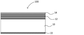
- FIG. 1 is a schematic cross-sectional view showing an example of the substrate 100 with a multilayer reflective film of the present embodiment.
- the substrate 100 with a multilayer reflective film shown in FIG. 1 includes a substrate 10, a multilayer reflective film 12 formed on the substrate 10, and a protective film 14 formed on the multilayer reflective film 12.
- a back surface conductive film 22 for an electrostatic chuck may be formed on the back surface of the substrate 10 (the surface opposite to the side on which the multilayer reflective film 12 is formed).
- the term "on” the substrate or film includes not only the case where it contacts the upper surface of the substrate or film but also the case where it does not contact the upper surface of the substrate or film. That is, the term “above” the substrate or film includes the case where a new film is formed above the substrate or film, the case where another film is interposed between the substrate or film, and the like. .. Further, “on” does not necessarily mean the upper side in the vertical direction. “On” merely indicates the relative positional relationship between the substrate and the film.
- the substrate 10 preferably has a low coefficient of thermal expansion within the range of 0 ⁇ 5 ppb / ° C. in order to prevent distortion of the transfer pattern due to heat during exposure with EUV light.
- a material having a low coefficient of thermal expansion in this range for example, SiO 2- TiO 2- based glass, multi-component glass ceramics, or the like can be used.
- the main surface on the side where the transfer pattern (absorbent pattern described later) of the substrate 10 is formed is processed in order to improve the flatness.
- the flatness is preferably 0.1 ⁇ m or less, more preferably 0.05 ⁇ m or less, and particularly preferably 0.05 ⁇ m or less in the region of 132 mm ⁇ 132 mm on the main surface on the side where the transfer pattern of the substrate 10 is formed. It is preferably 0.03 ⁇ m or less.
- the main surface (back surface) opposite to the side on which the transfer pattern is formed is a surface fixed to the exposure apparatus by an electrostatic chuck.
- the flatness is 0.1 ⁇ m or less, more preferably 0.05 ⁇ m or less, and particularly preferably 0.03 ⁇ m or less.
- the flatness is a value representing a surface warp (deformation amount) represented by TIR (Total Indicatored Reading).
- TIR Total Indicatored Reading
- the plane defined by the minimum square method with respect to the substrate surface is the focal plane, and the highest position of the substrate surface above the focal plane and the surface of the substrate below the focal plane are defined. It is the absolute value of the height difference from the lowest position.
- the surface roughness of the main surface of the substrate 10 on the side where the transfer pattern is formed is preferably 0.1 nm or less in terms of root mean square roughness (Rq).
- the surface roughness can be measured with an atomic force microscope.
- the substrate 10 preferably has high rigidity in order to prevent deformation of the film (multilayer reflective film 12 or the like) formed on the substrate 10 due to film stress.
- it is preferable to have a high Young's modulus of 65 GPa or more.
- the multilayer reflective film 12 has a structure in which a plurality of layers containing elements having different refractive indexes as main components are periodically laminated.
- the multilayer reflective film 12 has a thin film (high refractive index layer) of a light element or a compound thereof which is a high refractive index material and a thin film (low refractive index layer) of a heavy element or a compound thereof which is a low refractive index material. It is composed of a multilayer film in which and are alternately laminated for about 40 to 60 cycles.
- the high refractive index layer and the low refractive index layer may be laminated in this order for a plurality of cycles from the substrate 10 side. In this case, the laminated structure of one (high refractive index layer / low refractive index layer) has one cycle.
- the uppermost layer of the multilayer reflective film 12, that is, the surface layer of the multilayer reflective film 12 on the opposite side of the substrate 10 is preferably a high refractive index layer.
- the high refractive index layer and the low refractive index layer are laminated in this order from the substrate 10 side, the uppermost layer becomes the low refractive index layer.
- the low refractive index layer is the surface of the multilayer reflective film 12
- the low refractive index layer is easily oxidized, so that the reflectance of the surface of the multilayer reflective film is reduced. In that case, it is preferable to form a high refractive index layer on the low refractive index layer.
- the uppermost layer becomes the high refractive index layer.
- the uppermost high-refractive index layer becomes the surface of the multilayer reflective film 12.
- the high refractive index layer may be a layer containing Si.
- the high refractive index layer may contain Si alone or a Si compound.
- the Si compound may contain Si and at least one element selected from the group consisting of B, C, N, O and H.
- the low refractive index layer is selected from a layer containing at least one element selected from the group consisting of Mo, Ru, Rh, and Pt, or from the group consisting of Mo, Ru, Rh, and Pt. It may be a layer containing an alloy containing at least one element.
- a Mo / Si multilayer film in which Mo films and Si films are alternately laminated for about 40 to 60 cycles can be preferably used.
- the multilayer reflective film used in the region of EUV light for example, Ru / Si periodic multilayer film, Mo / Be periodic multilayer film, Mo compound / Si compound periodic multilayer film, Si / Nb periodic multilayer film, Si / Mo / Ru periodic multilayer films, Si / Mo / Ru / Mo periodic multilayer films, Si / Ru / Mo / Ru periodic multilayer films, Si / Ru / Mo / Ru periodic multilayer films, and the like can be used.
- the material of the multilayer reflective film can be selected in consideration of the exposure wavelength.
- the reflectance of such a multilayer reflective film 12 alone is, for example, 65% or more.
- the upper limit of the reflectance of the multilayer reflective film 12 is, for example, 73%.
- the thickness and period of the layers contained in the multilayer reflective film 12 can be selected so as to satisfy Bragg's law.
- the multilayer reflective film 12 can be formed by a known method.
- the multilayer reflective film 12 can be formed by, for example, an ion beam sputtering method.
- the multilayer reflective film 12 is a Mo / Si multilayer film
- a Mo film having a thickness of about 3 nm is formed on the substrate 10 by using an ion beam sputtering method using a Mo target.
- a Si film having a thickness of about 4 nm is formed using the Si target.
- the surface layer of the multilayer reflective film 12 on the opposite side of the substrate 10 is a layer containing Si (Si film).
- the thickness of the Mo / Si film in one cycle is 7 nm.
- the protective film 14 is formed on the multilayer reflective film 12 or in contact with the surface of the multilayer reflective film 12. be able to.
- the protective film 14 also has a function of protecting the multilayer reflective film 12 when correcting black defects in a transfer pattern using an electron beam (EB).
- EB electron beam
- the protective film 14 can be formed by a known method. Examples of the film forming method of the protective film 14 include an ion beam sputtering method, a magnetron sputtering method, a reactive sputtering method, a vapor deposition method (CVD), and a vacuum vapor deposition method.
- the protective film 14 may be continuously formed by an ion beam sputtering method after the multi-layer reflective film 12 is formed.
- the protective film 14 includes ruthenium (Ru), rhodium (Rh), titanium (Ti), zirconium (Zr), yttrium (Y), niobium (Nb), and vanadium. (V) and at least one additive element selected from hafnium (Hf).
- the protective film 14 contains ruthenium (Ru) and rhodium (Rh), the protective film 14 has etching resistance to a mixed gas of chlorine-based gas and oxygen gas, etching resistance to chlorine-based gas, etching resistance to fluorine-based gas, and sulfuric acid. Improves cleaning resistance due to overwater (SPM). If the content of Rh in the protective film 14 is too small, the effect of addition cannot be obtained. If the content of Rh in the protective film 14 is too large, the extinction coefficient k of the protective film 14 with respect to EUV light becomes high, so that the reflectance of the reflective mask 200 decreases. Therefore, the content of Rh in the protective film 14 is preferably 15 atomic% or more and 50 atomic% or less, and more preferably 20 atomic% or more and 40 atomic% or less.
- the protective film 14 is selected from ruthenium (Ru), rhodium (Rh), titanium (Ti), zirconium (Zr), yttrium (Y), niobium (Nb), vanadium (V), and hafnium (Hf).
- Ru ruthenium
- Rh rhodium
- Ti titanium
- Zr zirconium
- Y niobium
- Nb vanadium
- Hf hafnium
- the content of the additive element in the protective film 14 is preferably 1 atomic% or more and 20 atomic% or less.
- the protective film 14 contains titanium (Ti) as an additive element (for example, in the case of a RuRhTi film), the content of Ti in the protective film 14 is preferably 1 atomic% or more, and preferably 2 atomic% or more. Is more preferable. The Ti content is preferably 10 atomic% or less, more preferably 7 atomic% or less.
- the content of Zr in the protective film 14 is preferably 1 atomic% or more, preferably 2 atomic% or more. Is more preferable.
- the Zr content is preferably 10 atomic% or less, more preferably 7 atomic% or less.
- the protective film 14 contains yttrium (Y) as an additive element (for example, in the case of RuRhY film), the content of Y in the protective film 14 is preferably 1 atomic% or more, preferably 2 atomic% or more. Is more preferable.
- the Y content is preferably 10 atomic% or less, more preferably 7 atomic% or less.
- the content of Nb in the protective film 14 is preferably 1 atomic% or more, preferably 2 atomic% or more. Is more preferable.
- the Nb content is preferably 20 atomic% or less, and more preferably 15 atomic% or less.
- the protective film 14 contains vanadium (V) as an additive element (for example, in the case of RuRhV film), the content of V in the protective film 14 is preferably 1 atomic% or more, preferably 2 atomic% or more. Is more preferable.
- the V content is preferably 10 atomic% or less, more preferably 7 atomic% or less.
- the content of Hf in the protective film 14 is preferably 1 atomic% or more, preferably 2 atomic% or more. Is more preferable.
- the Hf content is preferably 7 atomic% or less, and more preferably 5 atomic% or less.
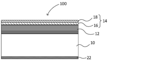
- FIG. 2 is a schematic cross-sectional view showing another example of the substrate 100 with a multilayer reflective film of the present embodiment.
- the protective film 14 may include a Si material layer 16 containing silicon (Si) on the side in contact with the multilayer reflective film 12. That is, the protective film 14 may include a Si material layer 16 on the side in contact with the multilayer reflective film 12 and a RuRh-based layer 18 formed on the Si material layer 16.
- the RuRh-based layer 18 has ruthenium (Ru), rhodium (Rh), titanium (Ti), zirconium (Zr), yttrium (Y), niobium (Nb), and vanadium (V), similarly to the protective film 14 described above.
- the Si material layer 16 is a layer made of a material containing silicon (Si).
- the Si material layer 16 includes, for example, silicon (Si), silicon oxide ( Si x O y (x, y is an integer of 1 or more) such as SiO, SiO 2 , Si 3 O 2 ), silicon nitride (SiN, Si 3). Selected from Si x N y (x, y is an integer of 1 or more) such as N 4 and silicon oxide (Si x O y N z (x, y, z is an integer of 1 or more) such as SiON). Contains at least one material.
- the Si material layer 16 is provided as the uppermost layer of the multilayer reflective film 12 when the multilayer reflective film 12 is a Mo / Si multilayer film and the Mo film and the Si film are laminated in this order from the substrate 10 side. It may be a Si film which is a refractive index layer.
- the Si material layer 16 contains a first noble gas element
- the RuRh-based layer 18 contains a second rare gas element different from the first rare gas element. But it may be.
- the first rare gas element and the second rare gas element may be one kind of rare gas element or two or more kinds of rare gas elements, respectively.
- the first rare gas element and the second rare gas element are "different", at least one rare gas element contained in the first rare gas element is contained in the second rare gas element. It means that it is different from the noble gas element of.
- the first noble gas element and the second noble gas element are at least one rare gas element selected from helium (He), neon (Ne), argon (Ar), krypton (Kr), and xenon (Xe), respectively.
- the first noble gas element and the second noble gas element preferably contain at least one noble gas element selected from argon (Ar), krypton (Kr), and xenon (Xe).
- the second rare gas element may have a smaller atomic weight than the first rare gas element.
- small as used herein means that the atomic weight of at least one rare gas element contained in the second rare gas element is smaller than the atomic weight of at least one rare gas element contained in the first rare gas element. Means that. For example, when the first noble gas element is krypton (Kr) and the second noble gas element is argon (Ar), such a condition is satisfied.
- the second rare gas element may have a larger atomic weight than the first rare gas element.
- the term "large” as used herein means that the atomic weight of at least one rare gas element contained in the second rare gas element is larger than the atomic weight of at least one rare gas element contained in the first rare gas element.
- the first noble gas element is argon (Ar) or krypton (Kr) and the second noble gas element is xenon (Xe)
- the first noble gas element is argon (Ar) and krypton (Kr) and the second noble gas element is argon (Ar) and xenon (Xe)
- such a condition is satisfied.
- the multilayer reflective film 12, the Si material layer 16, and the RuRh-based layer 18 may be formed by the same method or may be formed by different methods.
- the multilayer reflective film 12 and the Si material layer 16 may be continuously formed by an ion beam sputtering method, and then the RuRh-based layer 18 may be formed by a magnetron sputtering method.
- the multilayer reflective film 12 to the RuRh system layer 18 may be continuously formed by the ion beam sputtering method.
- the protective film 14 containing ruthenium (Ru), rhodium (Rh) and additive elements may be a single layer. It may be a multilayer film or a gradient film.
- the protective film 14 (RuRh-based layer 18) is used as a multilayer film, the additive element layer and the RuRh layer can be alternately laminated to form a multilayer film having 4 to 10 layers. In this case, it is preferable that the lowermost layer is an additive element layer and the uppermost layer is a RuRh layer.
- the protective film 14 (RuRh-based layer 18) is used as an inclined film
- the content of additive elements is large on the multilayer reflective film 12 side of the protective film 14 (RuRh-based layer 18), and the content of the additive element is large on the absorber film 24 side. It is preferable that the composition has a small content of additive elements.
- the protective film 14 (RuRh-based layer 18) is used as an inclined film
- the content of Rh is low on the multilayer reflective film 12 side of the protective film 14 (RuRh-based layer 18), and Rh on the absorber film 24 side. It is preferable to have a structure having a large content of.
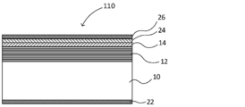
- FIG. 3 is a schematic cross-sectional view showing an example of the reflective mask blank 110 of the present embodiment.
- the reflective mask blank 110 shown in FIG. 3 has an absorber film 24 for absorbing EUV light on the protective film 14 of the substrate 100 with the multilayer reflective film described above.
- the reflective mask blank 110 may further have another thin film such as a resist film 26 on the absorber film 24.
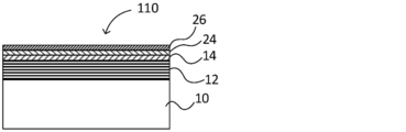
- FIG. 4 is a schematic cross-sectional view showing another example of the reflective mask blank 110 of the present embodiment.
- the reflective mask blank 110 may have an etching mask film 28 between the absorber film 24 and the resist film 26.
- the absorber film 24 of the reflective mask blank 110 of the present embodiment is formed on the protective film 14.
- the basic function of the absorber membrane 24 is to absorb EUV light.
- the absorber film 24 may be an absorber film 24 for the purpose of absorbing EUV light, or may be an absorber film 24 having a phase shift function in consideration of the phase difference of EUV light.
- the absorber film 24 having a phase shift function absorbs EUV light and reflects a part of the EUV light to shift the phase. That is, in the reflective mask 200 in which the absorber film 24 having a phase shift function is patterned, the portion where the absorber film 24 is formed absorbs EUV light and dims, and the pattern transfer is not adversely affected. Reflects some light.
- the absorber film 24 having a phase shift function is preferably formed so that the phase difference between the reflected light from the absorber film 24 and the reflected light from the multilayer reflective film 12 is 170 degrees to 190 degrees.
- the image contrast of the projected optical image is improved by the light having the inverted phase difference in the vicinity of 180 degrees interfering with each other at the pattern edge portion. As the image contrast is improved, the resolution is increased, and various exposure-related margins such as exposure amount margin and focal margin can be increased.
- the absorber membrane 24 may be a single-layer membrane or a multilayer membrane composed of a plurality of membranes (for example, a lower-layer absorber membrane and an upper-layer absorber membrane).
- a single-layer film the number of steps during mask blank manufacturing can be reduced, so that production efficiency is improved.
- its optical constant and film thickness can be appropriately set so that the upper layer absorber film becomes an antireflection film at the time of mask pattern defect inspection using light. This improves the inspection sensitivity at the time of mask pattern defect inspection using light.
- O oxygen
- N nitrogen
- the absorber film 24 By making the absorber film 24 a multilayer film in this way, it is possible to add various functions to the absorber film 24.
- the absorber film 24 has a phase shift function, the range of adjustment on the optical surface can be increased by forming the multilayer film, so that it becomes easy to obtain a desired reflectance.
- the material of the absorber film 24 has a function of absorbing EUV light and can be processed by etching or the like (preferably, it can be etched by dry etching of chlorine (Cl) -based gas and / or fluorine (F) -based gas).
- the material is not particularly limited as long as it is a material having a high etching selectivity with respect to the protective film 14 (RuRh-based layer 18).
- Those having such a function include palladium (Pd), silver (Ag), platinum (Pt), gold (Au), iridium (Ir), tungsten (W), chromium (Cr), cobalt (Co), and manganese.
- Mn tin
- Sn tantalum
- Ta vanadium
- V nickel
- Hf hafnium
- Fe iron
- Cu tellurium
- Zn magnesium
- Mg germanium
- Al aluminum
- Rh rhodium
- Ru ruthenium
- Mo molybdenum
- Nb niobium
- Ti titanium
- Zr zirconium
- Y ittrium
- At least one metal selected from silicon (Si), or compounds thereof, can be preferably used.
- the absorber film 24 can be formed by a magnetron sputtering method such as a DC sputtering method and an RF sputtering method.
- the absorber film 24 of a tantalum compound or the like can be formed by a reactive sputtering method using a target containing tantalum and boron and using argon gas to which oxygen or nitrogen is added.
- the tantalum compound for forming the absorber film 24 includes an alloy of Ta and the above-mentioned metal.
- the crystalline state of the absorber membrane 24 is preferably an amorphous or microcrystalline structure from the viewpoint of smoothness and flatness. If the surface of the absorber film 24 is not smooth or flat, the edge roughness of the absorber pattern 24a may increase and the dimensional accuracy of the pattern may deteriorate.
- the surface roughness of the absorber film 24 is preferably a root mean square roughness (Rms) of 0.5 nm or less, more preferably 0.4 nm or less, and further preferably 0.3 nm or less.
- Examples of the tantalum compound for forming the absorber film 24 include a compound containing Ta and B, a compound containing Ta and N, a compound containing Ta, O and N, Ta and B, and further O. Compounds containing at least one of and N, compounds containing Ta and Si, compounds containing Ta, Si and N, compounds containing Ta and Ge, compounds containing Ta, Ge and N, and the like. be able to.
- Ta is a material that has a large EUV light absorption coefficient and can be easily dry-etched with a chlorine-based gas or a fluorine-based gas. Therefore, it can be said that Ta is a material for the absorber membrane 24 having excellent processability. Further, by adding B, Si and / or Ge or the like to Ta, an amorphous material can be easily obtained. As a result, the smoothness of the absorber membrane 24 can be improved. Further, when N and / or O is added to Ta, the resistance of the absorber membrane 24 to oxidation is improved, so that the stability over time can be improved.
- a back surface conductive film 22 for an electrostatic chuck is formed on the second main surface of the substrate 100 (the main surface opposite to the side on which the multilayer reflective film 12 is formed).
- the sheet resistance required for the back surface conductive film 22 for an electrostatic chuck is usually 100 ⁇ / ⁇ ( ⁇ / square) or less.
- the back surface conductive film 22 can be formed by, for example, a magnetron sputtering method or an ion beam sputtering method using a target of a metal such as chromium or tantalum, or an alloy thereof.
- the material of the back surface conductive film 22 is preferably a material containing chromium (Cr) or tantalum (Ta).
- the material of the back surface conductive film 22 is preferably a Cr compound containing at least one selected from boron, nitrogen, oxygen, and carbon in Cr.
- the Cr compound include CrN, CrON, CrCN, CrCON, CrBN, CrBON, CrBCN and CrBOCN.
- the material of the back surface conductive film 22 is preferably Ta (tantalum), an alloy containing Ta, or a Ta compound containing at least one of boron, nitrogen, oxygen, and carbon in any of these.
- Ta compound examples include TaB, TaN, TaO, TaON, TaCON, TaBN, TaBO, TaBON, TaBCON, TaHf, TaHO, TaHN, TaHON, TaHON, TaHCON, TaSi, TaSiO, TaSiN, TaSiN, TaSiN, TaSiN, TaSiN , TaSiON, TaSiCON and the like.
- the film thickness of the back surface conductive film 22 is not particularly limited as long as it functions as a film for an electrostatic chuck, but is usually 10 nm to 200 nm. Further, the back surface conductive film 22 preferably has a function of adjusting the stress on the second main surface side of the reflective mask blank 110. That is, the back surface conductive film 22 is adjusted so that the reflective mask blank 110 is flat by balancing the stress generated by the formation of the thin film on the first main surface and the stress on the second main surface. It is preferable to have a function of
- An etching mask film 28 may be formed on the absorber film 24.
- the material of the etching mask film 28 it is preferable to use a material having a high etching selectivity of the absorber film 24 with respect to the etching mask film 28.
- the etching selectivity of the absorber film 24 with respect to the etching mask film 28 is preferably 1.5 or more, and more preferably 3 or more.
- the reflective mask blank 110 of the present embodiment preferably contains an etching mask film 28 containing chromium (Cr) on the absorber film 24.
- chromium chromium
- chromium compounds include materials containing Cr and at least one element selected from N, O, C and H.
- the etching mask film 28 more preferably contains CrN, CrO, CrC, CrON, CrOC, CrCN or CrOCN, and is a CrO-based film (CrO film, CrON film, CrOC film or CrOCN film) containing chromium and oxygen. Is more preferable.
- the etching mask film 28 containing chromium (Cr) is dried using a mixed gas of chlorine-based gas and oxygen gas. Damage to the protective film 14 when removing by etching can be suppressed.
- silicon or a silicon compound as the material of the etching mask film 28.
- silicon compounds include materials containing Si and at least one element selected from N, O, C and H, metallic silicon containing metal in silicon and the silicon compound (metal silicide), and metallic silicon compounds (metals). ⁇ Compound) and the like.
- metal silicon compound include a material containing a metal, Si, and at least one element selected from N, O, C, and H.
- the protective film 14 By configuring the protective film 14 to contain the above-mentioned ruthenium (Ru), rhodium (Rh) and additive elements, the protective film when the etching mask film 28 containing silicon is removed by dry etching using a fluorine-based gas. Damage to 14 can be suppressed.
- the film thickness of the etching mask film 28 is preferably 3 nm or more in order to form the pattern on the absorber film 24 with high accuracy.
- the film thickness of the etching mask film 28 is preferably 15 nm or less in order to reduce the film thickness of the resist film 26.
- the reflective mask 200 of the present embodiment can be manufactured by using the reflective mask blank 110 of the present embodiment.
- an example of a method for manufacturing a reflective mask will be described.
- 5A-E are schematic views showing an example of a method for manufacturing the reflective mask 200.
- the substrate 10, the multilayer reflective film 12 formed on the substrate 10, the protective film 14 formed on the multilayer reflective film 12, and the protective film 14 are formed.
- a reflective mask blank 110 having the absorber film 24 is prepared (FIG. 5A).
- a resist film 26 is formed on the absorber film 24 (FIG. 5B).
- a pattern is drawn on the resist film 26 by an electron beam drawing apparatus, and a resist pattern 26a is formed by further undergoing a developing and rinsing process (FIG. 5C).
- etching gas of the absorber film 24 for example, a fluorine-based gas and / or a chlorine-based gas can be used.
- Fluorine-based gases include CF 4 , CHF 3 , C2F 6 , C 3 F 6 , C 4 F 6 , C 4 F 8 , CH 2 F 2 , CH 3 F, C 3 F 8 , SF 6 , and F 2. Etc. can be used.
- chlorine-based gas Cl 2 , SiCl 4 , CHCl 3 , CCl 4 , BCl 3 , and the like can be used.
- a mixed gas containing a fluorine-based gas and / or a chlorine-based gas and O 2 in a predetermined ratio can be used.
- These etching gases may further contain an inert gas such as He and / or Ar, if desired.
- the resist pattern 26a is removed with a resist stripping solution.
- the reflective mask 200 of the present embodiment is obtained by undergoing a wet cleaning step using an acidic or alkaline aqueous solution (FIG. 5E).
- a pattern is formed on the etching mask film 28 using the resist pattern 26a as a mask. After that, a step of forming a pattern on the absorber film 24 using the etching mask pattern as a mask is added.
- the reflective mask 200 thus obtained has a configuration in which a multilayer reflective film 12, a protective film 14, and an absorber pattern 24a are laminated on a substrate 10.
- the region 30 where the multilayer reflective film 12 (including the protective film 14) is exposed has a function of reflecting EUV light.
- the region 32 in which the multilayer reflective film 12 (including the protective film 14) is covered with the absorber pattern 24a has a function of absorbing EUV light.
- the thickness of the absorber pattern 24a having a reflectance of, for example, 2.5% or less can be made thinner than before, so that a finer pattern can be transferred. Can be transferred to.
- a transfer pattern can be formed on the semiconductor substrate by lithography using the reflective mask 200 of the present embodiment. This transfer pattern has a shape in which the pattern of the reflective mask 200 is transferred.
- a semiconductor device can be manufactured by forming a transfer pattern on a semiconductor substrate with a reflective mask 200.
- FIG. 6 shows the pattern transfer device 50.
- the pattern transfer device 50 includes a laser plasma X-ray source 52, a reflective mask 200, a reduction optical system 54, and the like.
- An X-ray reflection mirror is used as the reduction optical system 54.
- the pattern reflected by the reflective mask 200 is usually reduced to about 1/4 by the reduction optical system 54.
- a wavelength band of 13 to 14 nm is used as the exposure wavelength, and the optical path is set in advance so as to be in a vacuum.
- the EUV light generated by the laser plasma X-ray source 52 is incident on the reflective mask 200.
- the light reflected by the reflective mask 200 is transferred onto the resisted semiconductor substrate 56 via the reduction optical system 54.
- the light reflected by the reflective mask 200 is incident on the reduction optical system 54.
- the light incident on the reduction optical system 54 forms a transfer pattern on the resist layer on the resisted semiconductor substrate 56.
- a resist pattern can be formed on the resisted semiconductor substrate 56.
- etching the semiconductor substrate 56 using the resist pattern as a mask for example, a predetermined wiring pattern can be formed on the semiconductor substrate.
- a semiconductor device is manufactured through such a process and other necessary steps.
- a 6025 size (about 152 mm ⁇ 152 mm ⁇ 6.35 mm) substrate 10 in which the first main surface and the second main surface were polished was prepared.
- the substrate 10 is a substrate made of low thermal expansion glass (SiO 2- TiO 2 glass).
- the main surface of the substrate 10 was polished by a rough polishing process, a precision polishing process, a local processing process, and a touch polishing process.
- the multilayer reflective film 12 was formed on the main surface (first main surface) of the substrate 10.
- the multilayer reflective film 12 formed on the substrate 10 is a periodic multilayer reflective film 12 composed of Mo and Si in order to obtain a multilayer reflective film 12 suitable for EUV light having a wavelength of 13.5 nm.
- the multilayer reflective film 12 was formed by alternately laminating Mo film and Si film on the substrate 10 by an ion beam sputtering method using a Mo target and a Si target and using krypton (Kr) as a process gas.
- a Si film was formed with a thickness of 4.2 nm
- a Mo film was formed with a thickness of 2.8 nm. This was set as one cycle, and 40 cycles were laminated in the same manner to form the multilayer reflective film 12.
- the Si material layer 16 was formed on the multilayer reflective film 12.
- the multilayer reflective film 12 and the Si material layer 16 were continuously formed by an ion beam sputtering method.
- a Si film was formed with a thickness of 4.0 nm using a Si target and krypton (Kr) as a process gas.
- a RuRh-based layer 18 or a Ru film was formed on the Si material layer 16.
- the RuRh-based layer 18 or the Ru film was formed with a film thickness shown in Table 1 by a magnetron sputtering method in an Ar gas atmosphere using a target having the composition shown in Table 1.
- the composition of the formed protective film 14 was measured by X-ray photoelectron spectroscopy (XPS).
- Table 1 shows the composition and film thickness of the protective film 14 (RuRh-based layer 18 or Ru film) in Examples and Comparative Examples.
- Reflective mask blank 110 Using the above-mentioned substrate 100 with a multilayer reflective film, a reflective mask blank 110 including an absorber film 24 was manufactured. Hereinafter, a method for manufacturing the reflective mask blank 110 will be described.
- the absorber film 24 was formed on the protective film 14 of the substrate 100 with the multilayer reflective film by the DC magnetron sputtering method.
- the absorber film 24 was a laminated film absorber film 24 composed of two layers, a TaN film which is an absorption layer and a TaO film which is a low reflection layer.
- a TaN film was formed as an absorption layer on the surface of the protective film 14 of the substrate 100 with the multilayer reflective film described above by a DC magnetron sputtering method.
- This TaN film was formed by a reactive sputtering method in a mixed gas atmosphere of Ar gas and N 2 gas in which a substrate 100 with a multilayer reflective film was opposed to a Ta target.
- a TaO film (low reflection layer) was formed on the TaN film by a DC magnetron sputtering method. Similar to the TaN film, this TaO film was formed by a reactive sputtering method in a mixed gas atmosphere of Ar and O 2 with the substrate 100 with a multilayer reflective film facing the Ta target.
- a back surface conductive film 22 made of CrN was formed on the second main surface (back side main surface) of the substrate 1 by a magnetron sputtering method (reactive sputtering method) under the following conditions.
- Conditions for forming the back surface conductive film 22 Cr target, mixed gas atmosphere of Ar and N 2 (Ar: 90 atomic%, N: 10 atomic%), film thickness 20 nm.
- the reflective mask blanks 110 of Examples 1 to 6 and Comparative Example 1 were manufactured.
- Reflective mask 200 Next, the reflective mask 200 was manufactured using the reflective mask blank 110 described above. The production of the reflective mask 200 will be described with reference to FIGS. 5A-E.
- a resist film 26 was formed on the absorber film 24 of the reflective mask blank 110. Then, a desired pattern such as a circuit pattern was drawn (exposed) on the resist film 26, and further developed and rinsed to form a predetermined resist pattern 26a (FIG. 5C). Next, using the resist pattern 26a as a mask, the TaO film (low reflection layer) of the absorber film 24 is dry-etched with CF 4 gas, and then the TaN film is dry-etched with Cl 2 gas. To form an absorber pattern 24a (FIG. 5D).
- the reflectance of the surface of the protective film 14 to EUV light having a wavelength of 13.5 nm was measured.
- the reflectance (reflectance after etching) of the surface of the protective film 14 not covered with the absorber pattern 24a was measured in the same manner.
- Table 1 shows changes in reflectance before and after etching the surface of the protective film 14 (absolute value of the difference between the reflectance before etching and the reflectance after etching).
- the presence or absence of blister generation was confirmed by observing the cross section of the reflective mask 200 with an electron microscope after taking out the reflective mask 200 from the exposure apparatus. The cross section of any 10 points was observed, and when even one blister generation was confirmed, it was determined that the blister generation was "presence".
- Multilayer Reflective Film 10 Substrate 12 Multilayer Reflective Film 14 Protective Film 16 Si Material Layer 18 RuRh System Layer 22 Backside Conductive 24 Absorbent Film 26 Resist Film 28 Etching Mask Film 100 Multilayer Reflective Film Substrate 110 Reflective Mask Blank 200 Reflective Mask
Landscapes
- Physics & Mathematics (AREA)
- General Physics & Mathematics (AREA)
- Preparing Plates And Mask In Photomechanical Process (AREA)
- Exposure And Positioning Against Photoresist Photosensitive Materials (AREA)
Abstract
La présente invention concerne un substrat équipé d'un film réfléchissant multicouche, une ébauche de masque réfléchissant, un masque réfléchissant et un procédé de production d'un dispositif à semi-conducteur, le substrat équipé d'un film réfléchissant multicouche ayant une tolérance élevée pour le gaz de gravure utilisé pour la gravure d'un film absorbeur et/ou d'un film de masque de gravure, et capable de supprimer l'apparition de cloques. Un substrat équipé d'un film réfléchissant multicouche 100 comprend un substrat 10, un film réfléchissant multicouche 12 disposé sur le substrat 10, et un film protecteur 14 disposé sur le film réfléchissant multicouche 12. Le film protecteur 14 contient au moins un élément supplémentaire choisi parmi du ruthénium (Ru), du rhodium (Rh), du titane (Ti), du zirconium (Zr), de l'yttrium (Y), du niobium (Nb), du vanadium (V) et de l'hafnium (Hf).
Priority Applications (3)
| Application Number | Priority Date | Filing Date | Title |
|---|---|---|---|
| US17/913,099 US20230133304A1 (en) | 2020-03-30 | 2021-03-22 | Multilayer reflective film-equipped substrate, reflective mask blank, reflective mask, and method for producing semiconductor device |
| KR1020227025437A KR20220161261A (ko) | 2020-03-30 | 2021-03-22 | 다층 반사막 부착 기판, 반사형 마스크 블랭크, 반사형 마스크, 및 반도체 장치의 제조 방법 |
| JP2022511950A JPWO2021200325A1 (fr) | 2020-03-30 | 2021-03-22 |
Applications Claiming Priority (2)
| Application Number | Priority Date | Filing Date | Title |
|---|---|---|---|
| JP2020059743 | 2020-03-30 | ||
| JP2020-059743 | 2020-03-30 |
Publications (1)
| Publication Number | Publication Date |
|---|---|
| WO2021200325A1 true WO2021200325A1 (fr) | 2021-10-07 |
Family
ID=77928727
Family Applications (1)
| Application Number | Title | Priority Date | Filing Date |
|---|---|---|---|
| PCT/JP2021/011620 WO2021200325A1 (fr) | 2020-03-30 | 2021-03-22 | Substrat équipé d'un film réfléchissant multicouche, ébauche de masque réfléchissant, masque réfléchissant et procédé de production d'un dispositif à semi-conducteur |
Country Status (5)
| Country | Link |
|---|---|
| US (1) | US20230133304A1 (fr) |
| JP (1) | JPWO2021200325A1 (fr) |
| KR (1) | KR20220161261A (fr) |
| TW (1) | TW202141166A (fr) |
| WO (1) | WO2021200325A1 (fr) |
Cited By (2)
| Publication number | Priority date | Publication date | Assignee | Title |
|---|---|---|---|---|
| WO2023199888A1 (fr) * | 2022-04-15 | 2023-10-19 | Agc株式会社 | Ébauche de masque réfléchissant, procédé de fabrication d'ébauche de masque réfléchissant, masque réfléchissant et procédé de fabrication de masque réfléchissant |
| WO2024005038A1 (fr) * | 2022-06-28 | 2024-01-04 | Hoya株式会社 | Substrat avec film réfléchissant multicouche, ébauche de masque réfléchissant, masque réfléchissant et procédé de production de dispositif semiconducteur |
Citations (5)
| Publication number | Priority date | Publication date | Assignee | Title |
|---|---|---|---|---|
| JP2006332153A (ja) * | 2005-05-24 | 2006-12-07 | Hoya Corp | 反射型マスクブランク及び反射型マスク並びに半導体装置の製造方法 |
| JP2014170931A (ja) * | 2013-02-11 | 2014-09-18 | Hoya Corp | 多層反射膜付き基板及びその製造方法、反射型マスクブランクの製造方法、反射型マスクの製造方法、並びに半導体装置の製造方法 |
| WO2015012151A1 (fr) * | 2013-07-22 | 2015-01-29 | Hoya株式会社 | Substrat à film réfléchissant multicouche, ébauche de masque réfléchissant pour lithographie euv, masque réfléchissant pour lithographie euv, son procédé de fabrication et procédé de fabrication de dispositif à semi-conducteurs |
| WO2015037564A1 (fr) * | 2013-09-11 | 2015-03-19 | Hoya株式会社 | Substrat ayant un film réfléchissant multicouche, ébauche de masque réfléchissant pour lithographie euv, masque réfléchissant pour lithographie euv, procédé de fabrication de masque réfléchissant pour lithographie euv, et procédé de fabrication de dispositif à semi-conducteurs |
| JP2016033956A (ja) * | 2014-07-31 | 2016-03-10 | 凸版印刷株式会社 | Euvマスク欠陥検査方法およびeuvマスクブランク |
Family Cites Families (1)
| Publication number | Priority date | Publication date | Assignee | Title |
|---|---|---|---|---|
| JP5371162B2 (ja) | 2000-10-13 | 2013-12-18 | 三星電子株式会社 | 反射型フォトマスク |
-
2021
- 2021-03-22 US US17/913,099 patent/US20230133304A1/en active Pending
- 2021-03-22 KR KR1020227025437A patent/KR20220161261A/ko unknown
- 2021-03-22 JP JP2022511950A patent/JPWO2021200325A1/ja active Pending
- 2021-03-22 WO PCT/JP2021/011620 patent/WO2021200325A1/fr active Application Filing
- 2021-03-25 TW TW110110904A patent/TW202141166A/zh unknown
Patent Citations (5)
| Publication number | Priority date | Publication date | Assignee | Title |
|---|---|---|---|---|
| JP2006332153A (ja) * | 2005-05-24 | 2006-12-07 | Hoya Corp | 反射型マスクブランク及び反射型マスク並びに半導体装置の製造方法 |
| JP2014170931A (ja) * | 2013-02-11 | 2014-09-18 | Hoya Corp | 多層反射膜付き基板及びその製造方法、反射型マスクブランクの製造方法、反射型マスクの製造方法、並びに半導体装置の製造方法 |
| WO2015012151A1 (fr) * | 2013-07-22 | 2015-01-29 | Hoya株式会社 | Substrat à film réfléchissant multicouche, ébauche de masque réfléchissant pour lithographie euv, masque réfléchissant pour lithographie euv, son procédé de fabrication et procédé de fabrication de dispositif à semi-conducteurs |
| WO2015037564A1 (fr) * | 2013-09-11 | 2015-03-19 | Hoya株式会社 | Substrat ayant un film réfléchissant multicouche, ébauche de masque réfléchissant pour lithographie euv, masque réfléchissant pour lithographie euv, procédé de fabrication de masque réfléchissant pour lithographie euv, et procédé de fabrication de dispositif à semi-conducteurs |
| JP2016033956A (ja) * | 2014-07-31 | 2016-03-10 | 凸版印刷株式会社 | Euvマスク欠陥検査方法およびeuvマスクブランク |
Cited By (2)
| Publication number | Priority date | Publication date | Assignee | Title |
|---|---|---|---|---|
| WO2023199888A1 (fr) * | 2022-04-15 | 2023-10-19 | Agc株式会社 | Ébauche de masque réfléchissant, procédé de fabrication d'ébauche de masque réfléchissant, masque réfléchissant et procédé de fabrication de masque réfléchissant |
| WO2024005038A1 (fr) * | 2022-06-28 | 2024-01-04 | Hoya株式会社 | Substrat avec film réfléchissant multicouche, ébauche de masque réfléchissant, masque réfléchissant et procédé de production de dispositif semiconducteur |
Also Published As
| Publication number | Publication date |
|---|---|
| KR20220161261A (ko) | 2022-12-06 |
| US20230133304A1 (en) | 2023-05-04 |
| TW202141166A (zh) | 2021-11-01 |
| JPWO2021200325A1 (fr) | 2021-10-07 |
Similar Documents
| Publication | Publication Date | Title |
|---|---|---|
| US11815807B2 (en) | Reflective mask blank, reflective mask, method of manufacturing reflective mask, and method of manufacturing semiconductor device | |
| US11815806B2 (en) | Reflective mask blank, reflective mask and manufacturing method thereof, and semiconductor device manufacturing method | |
| KR20190141083A (ko) | 반사형 마스크 블랭크, 반사형 마스크 및 반사형 마스크 블랭크의 제조 방법 | |
| WO2018135468A1 (fr) | Substrat doté d'un film conducteur, substrat doté d'un film réfléchissant multicouche, ébauche de masque réfléchissant, masque réfléchissant et procédé de fabrication de dispositif semi-conducteur | |
| JP2021056502A (ja) | 多層反射膜付き基板、反射型マスクブランク、反射型マスク及びその製造方法、並びに半導体装置の製造方法 | |
| WO2021200325A1 (fr) | Substrat équipé d'un film réfléchissant multicouche, ébauche de masque réfléchissant, masque réfléchissant et procédé de production d'un dispositif à semi-conducteur | |
| WO2020184473A1 (fr) | Ébauche de masque de type réflexion, masque de type réflexion et procédé pour le fabriquer, et procédé de fabrication de dispositif à semi-conducteur | |
| JP2019070854A (ja) | 反射型マスクブランク、反射型マスク及びその製造方法、並びに半導体装置の製造方法 | |
| JP7479884B2 (ja) | 多層反射膜付き基板、反射型マスクブランク、反射型マスク、及び半導体装置の製造方法 | |
| JP7354005B2 (ja) | 反射型マスクブランク、反射型マスク、及び半導体装置の製造方法 | |
| WO2022065144A1 (fr) | Substrat pourvu d'un film réfléchissant multicouche, ébauche de masque réfléchissant, procédé de fabrication de masque réfléchissant, et procédé de fabrication de dispositif semi-conducteur | |
| WO2022138434A1 (fr) | Substrat équipé d'un film réfléchissant multicouche, ébauche de masque réfléchissant, masque réfléchissant et procédé de production d'un dispositif à semi-conducteur | |
| TWI835798B (zh) | 反射型光罩基底、反射型光罩及其製造方法、以及半導體裝置之製造方法 | |
| JP7459399B1 (ja) | 反射型マスクブランク、反射型マスク及びその製造方法、並びに半導体装置の製造方法 | |
| WO2022210334A1 (fr) | Ébauche de masque réfléchissant, masque réfléchissant, procédé de fabrication de masque réfléchissant et procédé de fabrication de dispositif à semi-conducteur | |
| WO2022203024A1 (fr) | Ébauche de masque de type à réflexion, masque de type à réflexion, procédé pour la fabrication de masque de type à réflexion, et procédé pour la fabrication de dispositif à semi-conducteurs | |
| WO2022186004A1 (fr) | Substrat avec film réfléchissant multicouche, ébauche de masque réfléchissant, masque réfléchissant et procédé de fabrication de dispositif semi-conducteur | |
| JP2022087344A (ja) | 多層反射膜付き基板、反射型マスクブランク、反射型マスク、及び半導体デバイスの製造方法 |
Legal Events
| Date | Code | Title | Description |
|---|---|---|---|
| 121 | Ep: the epo has been informed by wipo that ep was designated in this application |
Ref document number: 21781055 Country of ref document: EP Kind code of ref document: A1 |
|
| ENP | Entry into the national phase |
Ref document number: 2022511950 Country of ref document: JP Kind code of ref document: A |
|
| NENP | Non-entry into the national phase |
Ref country code: DE |
|
| 122 | Ep: pct application non-entry in european phase |
Ref document number: 21781055 Country of ref document: EP Kind code of ref document: A1 |