WO2021200263A1 - 実装装置 - Google Patents
実装装置 Download PDFInfo
- Publication number
- WO2021200263A1 WO2021200263A1 PCT/JP2021/011330 JP2021011330W WO2021200263A1 WO 2021200263 A1 WO2021200263 A1 WO 2021200263A1 JP 2021011330 W JP2021011330 W JP 2021011330W WO 2021200263 A1 WO2021200263 A1 WO 2021200263A1
- Authority
- WO
- WIPO (PCT)
- Prior art keywords
- semiconductor chip
- mounting device
- attachment
- film substrate
- mounting
- Prior art date
- Legal status (The legal status is an assumption and is not a legal conclusion. Google has not performed a legal analysis and makes no representation as to the accuracy of the status listed.)
- Ceased
Links
Images



Classifications
-
- H—ELECTRICITY
- H10—SEMICONDUCTOR DEVICES; ELECTRIC SOLID-STATE DEVICES NOT OTHERWISE PROVIDED FOR
- H10W—GENERIC PACKAGES, INTERCONNECTIONS, CONNECTORS OR OTHER CONSTRUCTIONAL DETAILS OF DEVICES COVERED BY CLASS H10
- H10W72/00—Interconnections or connectors in packages
- H10W72/071—Connecting or disconnecting
- H10W72/0711—Apparatus therefor
-
- H—ELECTRICITY
- H10—SEMICONDUCTOR DEVICES; ELECTRIC SOLID-STATE DEVICES NOT OTHERWISE PROVIDED FOR
- H10P—GENERIC PROCESSES OR APPARATUS FOR THE MANUFACTURE OR TREATMENT OF DEVICES COVERED BY CLASS H10
- H10P72/00—Handling or holding of wafers, substrates or devices during manufacture or treatment thereof
- H10P72/04—Apparatus for manufacture or treatment
- H10P72/0446—Apparatus for mounting on conductive members, e.g. leadframes or conductors on insulating substrates
-
- H—ELECTRICITY
- H10—SEMICONDUCTOR DEVICES; ELECTRIC SOLID-STATE DEVICES NOT OTHERWISE PROVIDED FOR
- H10W—GENERIC PACKAGES, INTERCONNECTIONS, CONNECTORS OR OTHER CONSTRUCTIONAL DETAILS OF DEVICES COVERED BY CLASS H10
- H10W72/00—Interconnections or connectors in packages
- H10W72/071—Connecting or disconnecting
- H10W72/0711—Apparatus therefor
- H10W72/07118—Means for cleaning, e.g. brushes
-
- H—ELECTRICITY
- H10—SEMICONDUCTOR DEVICES; ELECTRIC SOLID-STATE DEVICES NOT OTHERWISE PROVIDED FOR
- H10W—GENERIC PACKAGES, INTERCONNECTIONS, CONNECTORS OR OTHER CONSTRUCTIONAL DETAILS OF DEVICES COVERED BY CLASS H10
- H10W72/00—Interconnections or connectors in packages
- H10W72/071—Connecting or disconnecting
- H10W72/0711—Apparatus therefor
- H10W72/07141—Means for applying energy, e.g. ovens or lasers
-
- H—ELECTRICITY
- H10—SEMICONDUCTOR DEVICES; ELECTRIC SOLID-STATE DEVICES NOT OTHERWISE PROVIDED FOR
- H10W—GENERIC PACKAGES, INTERCONNECTIONS, CONNECTORS OR OTHER CONSTRUCTIONAL DETAILS OF DEVICES COVERED BY CLASS H10
- H10W72/00—Interconnections or connectors in packages
- H10W72/071—Connecting or disconnecting
- H10W72/0711—Apparatus therefor
- H10W72/07163—Means for mechanical processing, e.g. for planarising, pressing, stamping or drilling
-
- H—ELECTRICITY
- H10—SEMICONDUCTOR DEVICES; ELECTRIC SOLID-STATE DEVICES NOT OTHERWISE PROVIDED FOR
- H10W—GENERIC PACKAGES, INTERCONNECTIONS, CONNECTORS OR OTHER CONSTRUCTIONAL DETAILS OF DEVICES COVERED BY CLASS H10
- H10W72/00—Interconnections or connectors in packages
- H10W72/071—Connecting or disconnecting
- H10W72/0711—Apparatus therefor
- H10W72/07178—Means for aligning
-
- H—ELECTRICITY
- H10—SEMICONDUCTOR DEVICES; ELECTRIC SOLID-STATE DEVICES NOT OTHERWISE PROVIDED FOR
- H10W—GENERIC PACKAGES, INTERCONNECTIONS, CONNECTORS OR OTHER CONSTRUCTIONAL DETAILS OF DEVICES COVERED BY CLASS H10
- H10W72/00—Interconnections or connectors in packages
- H10W72/071—Connecting or disconnecting
- H10W72/072—Connecting or disconnecting of bump connectors
- H10W72/07251—Connecting or disconnecting of bump connectors characterised by changes in properties of the bump connectors during connecting
- H10W72/07255—Connecting or disconnecting of bump connectors characterised by changes in properties of the bump connectors during connecting changes in materials
-
- H—ELECTRICITY
- H10—SEMICONDUCTOR DEVICES; ELECTRIC SOLID-STATE DEVICES NOT OTHERWISE PROVIDED FOR
- H10W—GENERIC PACKAGES, INTERCONNECTIONS, CONNECTORS OR OTHER CONSTRUCTIONAL DETAILS OF DEVICES COVERED BY CLASS H10
- H10W72/00—Interconnections or connectors in packages
- H10W72/20—Bump connectors, e.g. solder bumps or copper pillars; Dummy bumps; Thermal bumps
- H10W72/251—Materials
- H10W72/255—Materials of outermost layers of multilayered bumps, e.g. material of a coating
-
- H—ELECTRICITY
- H10—SEMICONDUCTOR DEVICES; ELECTRIC SOLID-STATE DEVICES NOT OTHERWISE PROVIDED FOR
- H10W—GENERIC PACKAGES, INTERCONNECTIONS, CONNECTORS OR OTHER CONSTRUCTIONAL DETAILS OF DEVICES COVERED BY CLASS H10
- H10W95/00—Packaging processes not covered by the other groups of this subclass
Definitions
- the present invention relates to a mounting device for mounting a semiconductor chip on a film substrate.
- Chip-on-film (Chip on Film; hereinafter referred to as COF) mounting which mounts a semiconductor chip on a film substrate, has been used for applications such as driver ICs for displays, but these days, the impact of narrowing the cost of mobile terminals, etc. Demand is expanding. For this reason, the demand for mounting devices for COF mounting is also increasing.
- FIG. 6 shows an example of a mounting device that mounts COF by a flip chip method. It is to be mounted on a flip chip.
- the metals are directly bonded to each other so that reliability can be obtained even if the electrode pitch is narrow.
- gold-tin eutectic bonding is mainly used.
- Both electrodes need to be heated to a high temperature in order to perform gold-tin eutectic bonding, the heater portion 22 of the bonding head 2 is heated to about 400 ° C., and the semiconductor chip C adsorbed and held on the lower surface of the heater portion 22 is attached.
- the electrodes of the semiconductor chip C and the electrodes provided on the film substrate F are heated and pressed in a state of being in close contact with each other to join them.
- the cleaning means 7 is included as a component, and the deposits on the lower surface of the heater 22 are removed by the grindstone 71 provided in the cleaning means 7.
- the bonding head 2 is periodically moved from the state facing the stage 3 to a position facing the cleaning means 7, and the heater 22 and the grindstone 71 are moved relative to each other in the XY plane while being in close contact with each other. Since the degree of dirt adhesion to the lower surface of the heater 22 differs depending on various conditions such as the difference in the wafer W, the time required for cleaning tends to be set longer with an emphasis on certainty.
- the present invention has been made in view of the above problems, and provides a mounting device having a short cycle time and excellent productivity when mounting a semiconductor chip on a film substrate.
- the invention according to claim 1 is A mounting device that joins an electrode on a film substrate and an electrode of the semiconductor chip by heating and pressurizing the semiconductor chip on the film substrate, and mounts the semiconductor chip on the film substrate.
- a bonding head having a heater portion for heating the semiconductor chip and an attachment detachably provided at a position connected to the heater portion and having a surface for pressurizing the semiconductor chip, and the semiconductor chip formed by the bonding head.
- It is a mounting device including a substrate stage that supports a pressurized region from the film substrate side when pressure is applied, and an attachment conveying means that conveys the attachment when the attachment is attached or detached.
- the invention according to claim 2 is the mounting device according to claim 1.
- One electrode of the electrode on the film substrate and the electrode of the semiconductor chip is gold-plated, the other is tin-plated, and both electrodes are gold-tin eutectic bonded by heating.
- the invention according to claim 4 is the mounting device according to any one of claims 1 to 3.
- the attachment transport means is a mounting device having a built-in heater.
- the invention according to claim 5 is the mounting apparatus according to any one of claims 1 to 4. It is further equipped with an upper and lower two-field camera for aligning the film substrate and the semiconductor chip before mounting.
- the attachment transporting means is a mounting device connected to the upper and lower two-field cameras.
- the invention according to claim 6 is the mounting device according to any one of claims 1 to 5. It is a mounting device further provided with a cleaning means for cleaning the attachment in a state of being removed from the bonding head.
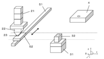
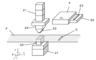
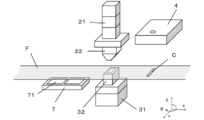
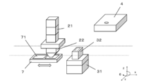
- FIG. 1 It is a figure which shows the structure of the mounting apparatus which concerns on embodiment of this invention. It is a figure explaining the main part which concerns on embodiment of this invention. It is a figure which shows the state which the mounting apparatus which concerns on embodiment of this invention attaches / detaches an attachment. It is a figure which shows another form of the attachment transport means which concerns on embodiment of this invention.
- This is a conventional example of a mounting device for mounting a semiconductor chip on a film substrate. It is a figure which shows the main part of the mounting apparatus which mounts a semiconductor chip on a film substrate. It is a figure which shows the state which cleans the semiconductor chip adsorption surface in the conventional example of the mounting apparatus which mounts a semiconductor chip on a film substrate.
- FIG. 1 is a diagram showing a configuration of a mounting device 1 according to an embodiment of the present invention
- FIG. 2 is a diagram showing a configuration of a main part of the mounting device 1.
- the mounting device 1 of FIG. 1 is a device for mounting the semiconductor chip C on the film substrate F, and joins the bump which is the electrode of the semiconductor chip C and the electrode of the film substrate F.
- the bump of the semiconductor chip C is gold-plated
- the electrode of the film substrate F is tin-plated
- both electrodes are eutectic-bonded with gold-tin by heating.
- the present invention is not limited to this, and the bumps of the semiconductor chip C may be tin-plated, the electrodes of the film substrate F may be gold-plated, and further, when both electrodes are joined. It can be used for mounting that requires high temperature.
- the film substrate F has an electrode pattern formed on the surface of a resin film such as polyimide having heat resistance, and the semiconductor chip C is mounted at a predetermined position while being sequentially conveyed.
- the film substrate F is continuously conveyed by a film conveying mechanism (not shown), and FIG. 1 shows an example in which the film substrate F is conveyed from left to right.
- the bonding head 2 has a function of holding and heating the semiconductor chip C, and also has a function of moving up and down (Z direction) by a head drive unit (not shown) to pressurize the semiconductor chip C on the facing surface. Have. Further, the bonding head 2 can be moved in the XY direction and the ⁇ direction, which is the rotation direction with respect to the Z axis, by the head drive unit.
- the bonding head 2 is composed of a head body 21, a heater unit 22, and an attachment 22.
- the head body 21 is driven by the head drive unit while holding the heater unit 22 on the lower side and blocking the heat of the heater unit 22.
- the heater unit 22 heats the semiconductor chip C via the attachment 23, and has a built-in electric heater.
- the electric heater in the present invention is premised on a constant heater having a heating temperature of 400 ° C. or higher, but the effect of the present invention is large when the heating temperature is 450 ° C. or higher, and a remarkable effect can be obtained at 500 ° C. or higher. Further, as long as the heating temperature is 450 ° C. or higher, the heater is not limited to the constant heater, and may be a ceramic heater.
- the attachment 23 has a surface that is in close contact with the semiconductor chip C, and also has a function of transferring the heat generated by the heater unit 22 to the semiconductor chip C.
- the attachment 23 is detachably provided with respect to the heater portion 22 so as to be attracted and held by the heater portion 22.
- the material of the heater portion 22 and the attachment 23 is selected from metal and ceramics having excellent heat resistance and heat transfer properties including dimensional stability.
- the stage 3 supports the pressurizing region from the film substrate F side when the semiconductor chip C and the film substrate F are pressurized by the bonding head 2, and is composed of the stage body 31 and the stage attachment 32.
- the main body 31 may have a function of raising the temperature of the stage attachment 32 by incorporating an electric heater.
- there may be a stage drive unit that drives the stage 3 in the XY direction or the Z direction.
- the upper and lower two-view camera 4 observes the relative position in order to align the semiconductor chip C and the film substrate F so that the bumps of the semiconductor chip C and the electrodes of the film substrate F are aligned. It may be movable in a direction and may have a function of moving in the Z direction. Specifically, the alignment mark on the bump-side surface of the semiconductor chip C and the alignment mark on the electrode-side surface of the film substrate F are observed to grasp the relative positions of the two. After observing the relative position, the bonding head 2 and the like are adjusted in the XY plane and in the ⁇ direction for alignment.
- the attachment transporting means 5 carries out the attachment 23 detached from the heater portion 22 and carries in the attachment 23 to be attached to the heater portion 22, and in FIGS. 1 and 2, the slide rail 51 and the attachment 23 are held.
- An example of the table 52 moving on the slide rail 51 is shown.
- the table 52 preferably has a function of sucking and holding the attachment 23, and may have a built-in heater for heating the attachment 23.
- the chip supply means 6 has a function of picking up the semiconductor chip C from the diced wafer W and delivering it to the bonding head 2.
- the chip supply means 6 pushes up the wafer W from the dicing tape side by the needle mechanism 63, sucks and holds the pushed-up semiconductor chip C by the chip picker 62, reverses it, and conveys it to the bonding head side along the slide rail 61. Is.
- the timing at which the attachment 23 is replaced by the mounting device 1 is basically the same as the timing at which the conventional mounting device cleans the lower surface of the heater 22.
- the procedure is as follows. That is, (1) The bonding head 2 moves onto the table 52 (FIG. 3) to release the suction of the attachment 23 and hands it over to the table 52. (2) The table 52 moves and the used attachment 23 is discharged. (3) The table 52 is equipped with a new attachment 23 and moves under the bonding head 2. (4) The new attachment 23 is delivered to the bonding head 2 (FIG. 3), (5) The bonding head 2 moves to a predetermined position for mounting, Will be.
- the procedure for replacing the attachment 23 in this way can be performed in a shorter time than cleaning the lower surface of the conventional heater 22, and the attachment 23 is replaced with an attachment 23 whose surface in close contact with the semiconductor chip C is surely cleaned. Is possible. Further, when the attachment 23 is attached / detached and conveyed, fine powder such as shavings is not generated.
- the table 52 has a built-in heater, it is preferable because the attachment 23 is heated to the extent that it can be thermocompression bonded immediately after the new attachment 23 is delivered to the bonding tool 2.
- the procedure described above can be shortened as follows, i.e. (1) The bonding head 2 moves onto the table 52 on which the new attachment 23 is mounted, releases the suction of the attachment 23, and delivers it to the table 52. (2) Hand over the new attachment 23 to the bonding head 2 and (3) The bonding head 2 moves to a predetermined position for mounting, Can also be shortened.
- the mounting device shown in FIG. 1 is provided with a slide rail 51 for moving the table 52 as the attachment transporting means 5, but the present invention is not limited to this.
- the table 52 may be provided so as to be connected to the upper and lower two-field cameras that can move in the XY directions.
- the attachment 23 removed from the bonding head 2 can be reused by cleaning.
- a cleaning device may be provided separately from the mounting device, but the mounting device may be configured to include cleaning means for the attachment. If the main component of the deposit adhering to the attachment 23 is an organic substance, a cleaning means using an organic solvent may be provided. Such cleaning with an organic solvent has been difficult to use for cleaning the lower surface of the heater 22 with a conventional mounting device, but it can be adopted by adopting a method of impacting an attachment tool.
Landscapes
- Wire Bonding (AREA)
Abstract
半導体チップをフィルム基板に実装するのに際して、サイクルタイムが短く、生産性に優れた実装装置提供すること。具体的には、フィルム基板上の半導体チップを加熱および加圧することで、前記フィルム基板上の電極と前記半導体チップの電極を接合して、前記半導体チップを前記フィルム基板に実装する実装装置であって、前記半導体チップを加熱するヒータ部と、前記ヒータ部と連結した位置に脱着可能に設けられ、前記半導体チップを加圧する面を備えたアタッチメントと、を有するボンディングヘッドと、前記ボンディングヘッドによる前記半導体チップの可圧時に、加圧領域を前記フィルム基板側から支持する基板ステージと、前記アタッチメント脱着時に、前記アタッチメントを搬送するアタッチメント搬送手段とを備えた実装装置を提供する。
Description
本発明はフィルム基板上に半導体チップを実装する実装装置に関する。
フィルム基板に半導体チップを実装するチップオンフィルム(Chip on Film;以下COFと記す)実装は従来よりディスプレイ用ドライバIC等の用途に用いられているが、昨今では携帯端末の狭額化の影響等により需要が拡大している。このため、COF実装を行う実装装置の需要も高まっている。
特に、画像の高精細化の進捗に伴い、電極ピッチが狭い半導体チップの実装に適したフリップチップ方式のCOF実装が主流となってきている。
図5(および図5の主要部を拡大した)図6は、フリップチップ方式でCOF実装を行う実装装置の一例を示すもので、ダイシング済のウェハWから半導体チップCをピックアップしてフィルム基板Fにフリップチップ実装するものである。ここで、半導体チップCの電極であるバンプとフィルム基板Fの接合は、電極ピッチが狭くても信頼性が得られるよう金属同士を直接接合している。具体的には、金錫共晶接合が主に用いられている。
金錫共晶接合を行うために両電極を高温に加熱する必要があり、ボンディングヘッド2のヒータ部22は400℃程度まで昇温され、ヒータ部22の下面に吸着保持された半導体チップCが加熱され、半導体チップCの電極とフィルム基板Fに設けられた電極が対向密着した状態で加圧されることで接合する。
図5およ図6の実装装置において、半導体チップCの実装を繰り返し行うことにより、半導体チップCを吸着保持するヒータ22の下面に付着した汚れが硬化しながら堆積されていくことが知られている(特許文献1等)。このような堆積物は、半導体チップCの吸着、加圧および加熱に悪影響を及ぼすことから、適宜除去する必要がある。
このため、一定回数の実装を行った後にヒータ22の下面を清掃する機構を実装装置に組み込むことが多い。
図5および図6においては、清掃手段7が構成要素として含まれており、清掃手段7に設けた砥石71によりヒータ22の下面の堆積物除去している。具体的には、ボンディングヘッド2がステージ3と対向する状態から、定期的に清掃手段7と対向する位置に移動し、ヒータ22と砥石71を密着させながらXY面内で相対移動させている。なお、ヒータ22の下面への汚れ付着の度合いは、ウェハWの違い等の種々の条件の違いによって異なるため、清掃に要する時間は確実性を重視して長めに設定する傾向がある。
このような清掃は、比較的簡単な構成で自動的に行えるため、オペレータに対する負荷は小さい。ただし、清掃に要する時間は、実装装置としての実稼働率を低下させている。また、砥石71で汚れを除去する場合、削りカスが装置内に飛散し、実装品質に悪影響を及ぼす懸念もあり、削りカスを回収する機構を付加すると装置のコストアップになる。
さらに、昨今では、実装のサイクルタイムを短縮する一環として、加熱温度の高温化が進んでおり、ヒータ22の温度に対する要求も500℃前後に達している。このようなヒータ22の温度上昇により実装1回毎の時間は短縮される一方で、汚れの硬化および堆積も加速される傾向にあり、従来以上の高頻度でヒータ22の下面を清掃する必要が生じており、サイクルタイム短縮に見合った生産性向上にはなっていない。
本発明は上記問題に鑑みてなされたものであり、半導体チップをフィルム基板に実装するのに際して、サイクルタイムが短く、生産性に優れた実装装置を提供するものである。
上記課題を解決するために、請求項1に記載の発明は、
フィルム基板上の半導体チップを加熱および加圧することで、前記フィルム基板上の電極と前記半導体チップの電極を接合して、前記半導体チップを前記フィルム基板に実装する実装装置であって、
前記半導体チップを加熱するヒータ部と、前記ヒータ部と連結した位置に脱着可能に設けられ、前記半導体チップを加圧する面を備えたアタッチメントと、を有するボンディングヘッドと、前記ボンディングヘッドによる前記半導体チップの可圧時に、加圧領域を前記フィルム基板側から支持する基板ステージと、前記アタッチメント脱着時に、前記アタッチメントを搬送するアタッチメント搬送手段とを備えた実装装置である。
フィルム基板上の半導体チップを加熱および加圧することで、前記フィルム基板上の電極と前記半導体チップの電極を接合して、前記半導体チップを前記フィルム基板に実装する実装装置であって、
前記半導体チップを加熱するヒータ部と、前記ヒータ部と連結した位置に脱着可能に設けられ、前記半導体チップを加圧する面を備えたアタッチメントと、を有するボンディングヘッドと、前記ボンディングヘッドによる前記半導体チップの可圧時に、加圧領域を前記フィルム基板側から支持する基板ステージと、前記アタッチメント脱着時に、前記アタッチメントを搬送するアタッチメント搬送手段とを備えた実装装置である。
請求項2に記載の発明は、請求項1に記載の実装装置であって、
前記ヒータ部が450℃以上に昇温可能な実装装置である
請求項3に記載の発明は、請求項1または請求項2に記載の実装装置であって、
前記フィルム基板上の電極と前記半導体チップの電極の一方の電極は金メッキを施され、他方が錫メッキを施され、加熱により両電極が金錫共晶接合される実装装置である。
前記ヒータ部が450℃以上に昇温可能な実装装置である
請求項3に記載の発明は、請求項1または請求項2に記載の実装装置であって、
前記フィルム基板上の電極と前記半導体チップの電極の一方の電極は金メッキを施され、他方が錫メッキを施され、加熱により両電極が金錫共晶接合される実装装置である。
請求項4に記載の発明は、請求項1から請求項3の何れかに記載の実装装置であって、
前記アタッチメント搬送手段がヒータを内蔵している実装装置である。
前記アタッチメント搬送手段がヒータを内蔵している実装装置である。
請求項5に記載の発明は、請求項1から請求項4の何れかに記載の実装装置であって、
実装前のフィルム基板と半導体チップの位置合わせをするための上下2視野カメラを更に備え、
前記アタッチメント搬送手段が前記上下2視野カメラに連結された実装装置である。
実装前のフィルム基板と半導体チップの位置合わせをするための上下2視野カメラを更に備え、
前記アタッチメント搬送手段が前記上下2視野カメラに連結された実装装置である。
請求項6に記載の発明は、請求項1から請求項5の何れかに記載の実装装置であって、
前記ボンディングヘッドから外された状態の前記アタッチメントを洗浄する洗浄手段を更に備えた実装装置である。
前記ボンディングヘッドから外された状態の前記アタッチメントを洗浄する洗浄手段を更に備えた実装装置である。
本発明により、半導体チップをフィルム基板に実装するのに際して、サイクルタイムが短く、生産性に優れた実装装置が提供される。
本発明の実施形態を図面を用いて説明する。図1は本発明の実施形態に係る実装装置1の構成を示す図であり、図2は実装装置1の主要部分の構成を示す図である。図1の実装装置1は、半導体チップCをフィルム基板Fに実装する装置であり、半導体チップCの電極であるバンプとフィルム基板Fの電極を接合するものである。
本実施形態において半導体チップCのバンプは金メッキを施されたもので、フィルム基板Fの電極は錫メッキを施されたものであり、加熱により両電極が金錫共晶接合されるものである。ただし、本発明はこれに限定されるものではなく、半導体チップCのバンプに錫メッキが施され、フィルム基板Fの電極に金メッキが施されたものでもよく、更には、両電極を接合する際に高温が必要な実装に利用できるものである。
また、フィルム基板Fは耐熱性を有するポリイミド等の樹脂フィルム表面に電極パターンが形成されたもので、順次搬送されながら所定位置に半導体チップCが実装されるものである。フィルム基板Fは図示していないフィルム搬送機構により連続的に搬送されるもので、図1ではフィルム基板Fが左から右に搬送される例を示している。
ボンディングヘッド2は、半導体チップCを保持して加熱する機能を有しているとともに、図示していないヘッド駆動ユニットにより上下(Z方向)に移動して半導体チップCを対向面に加圧する機能を有している。また、ボンディングヘッド2はヘッド駆動ユニットにより、XY方向および、Z軸に対する回転方向であるθ方向に移動可能となっている。
ボンディングヘッド2は、図2に示すように、ヘッド本体21、ヒータ部22、アタッチメント22によって構成されている。ヘッド本体21はヒータ部22を下側に保持しつつ、ヒータ部22の熱を遮断した状態でヘッド駆動ユニットによって駆動される。ヒータ部22は、アタッチメント23を介して半導体チップCを加熱するもので電熱ヒータを内蔵している。なお、本発明における電熱ヒータとして加熱温度が400℃以上のコンスタントヒータを前提としているが、加熱温度が450℃以上の場合に発明の効果が大きく、500℃以上で顕著な効果が得られる。また、加熱温度が450℃以上であればコンスタントヒータに限定されるものではなく、セラミックヒータであっても良い。
アタッチメント23は、半導体チップCと密着する面を有し、ヒータ部22で発生した熱を半導体チップCに伝える機能も有している。本発明において、アタッチメント23はヒータ部22に対して脱着可能に設けられており、ヒータ部22に吸着保持されるようになっている。なお、ヒータ部22、アタッチメント23の材質としては、寸法安定性も含む耐熱性、伝熱性に優れた、金属やセラミックスから選定される。
ステージ3は、ボンディングヘッド2によって半導体チップCとフィルム基板Fを加圧する際に、加圧領域をフィルム基板F側から支持するものであり、ステージ本体31とステージアタッチメント32から構成されるが、ステージ本体31に電熱ヒータを内蔵するなどして、ステージアタッチメント32を昇温する機能を備えていてもよい。また、ステージ3をXY方向やZ方向に駆動するステージ駆動ユニットがあってもよい。
上下2視野カメラ4は、半導体チップCのバンプとフィルム基板Fの電極の位置が合うように、半導体チップCとフィルム基板Fの位置合わせを行うために相対位置の観察を行うものであり、XY方向に移動可能でありZ方向に移動する機能を備えていてもよい。具体的には、半導体チップCのバンプ側の面にあるアライメントマークと、フィルム基板Fの電極側の面にあるアライメントマークを観察して両者の相対位置を掌握するものである。相対位置観察後は、位置合わせのために、ボンディングヘッド2等をXY面内およびθ方向で調整する。
アタッチメント搬送手段5は、ヒータ部22から外れたアタッチメント23の搬出および、ヒータ部22に装着するアタッチメント23の搬入を行うものであり、図1および図2では、スライドレール51と、アタッチメント23を保持し、スライドレール51上を移動するテーブル52によって構成される例を示している。ここで、テーブル52はアタッチメント23を吸着保持する機能を有していることが好ましく、アタッチメント23を加熱するヒータを内蔵していてもよい。
チップ供給手段6は、ダイシングされたウェハWから半導体チップCをピックアップして、ボンディングヘッド2に受け渡す機能を有するものである。チップ供給手段6は、ウェハWをダイシングテープ側からニードル機構63で突き上げ、突き上げられた半導体チップCをチップピッカ62が吸着保持してから反転させ、スライドレール61に沿ってボンディングヘッド側に搬送するものである。
実装装置1でアタッチメント23を交換するタイミングは、基本的に従来の実装装置がヒータ22の下面を清掃するタイミングと同様である。実装装置1では、アタッチメント23の交換に際して、以下の手順で進む。すなわち、
(1)ボンディングヘッド2がテーブル52の上に移動(図3)してアタッチメント23の吸着を解除してテーブル52に受け渡し、
(2)テーブル52が移動して、使用済みアタッチメント23を排出、
(3)テーブル52が新たなアタッチメント23を搭載し、ボンディングヘッド2の下に移動、
(4)新たなアタッチメント23をボンディングヘッド2に受け渡し(図3)、
(5)ボンディングヘッド2が実装を行う所定位置に移動、
となる。
(1)ボンディングヘッド2がテーブル52の上に移動(図3)してアタッチメント23の吸着を解除してテーブル52に受け渡し、
(2)テーブル52が移動して、使用済みアタッチメント23を排出、
(3)テーブル52が新たなアタッチメント23を搭載し、ボンディングヘッド2の下に移動、
(4)新たなアタッチメント23をボンディングヘッド2に受け渡し(図3)、
(5)ボンディングヘッド2が実装を行う所定位置に移動、
となる。
このようにアタッチメント23を交換する手順は、従来のヒータ22下面を清掃するのに比べて短時間で行うことが出来るとともに、半導体チップCと密着する面を確実に清掃したアタッチメント23に交換することが可能である。更に、アタッチメント23を脱着および搬送するのに際して削りカスのような微粉末が発生するようなこともない。
さらに、テーブル52がヒータを内蔵していれば、新たなアタッチメント23をボンディングツール2に受け渡した直後から、アタッチメント23が熱圧着を行える程度に加熱されるので好ましい。
また、テーブル52が2つのアタッチメント23を同時に保持できるものであるならば、上に説明した手順は以下のように短縮される、すなわち、
(1)ボンディングヘッド2が、新たなアタッチメント23を搭載したテーブル52の上に移動してアタッチメント23の吸着を解除してテーブル52に受け渡し、
(2)新たなアタッチメント23をボンディングヘッド2に受け渡し、
(3)ボンディングヘッド2が実装を行う所定位置に移動、
と短縮することもできる。
(1)ボンディングヘッド2が、新たなアタッチメント23を搭載したテーブル52の上に移動してアタッチメント23の吸着を解除してテーブル52に受け渡し、
(2)新たなアタッチメント23をボンディングヘッド2に受け渡し、
(3)ボンディングヘッド2が実装を行う所定位置に移動、
と短縮することもできる。
このように、本実施形態のように、アタッチメントツール23を交換することにより、実装作業以外のロス時間を減らすことが出来、実装装置の生産性が向上する。
なお、図1に示した実装装置においてアタッチメント搬送手段5として、テーブル52を移動させるためのスライドレール51を備えた構成となっているが、これに限定されるものではない。例えば、図4のようにXY方向に移動可能な上下2視野カメラに連結するようにテーブル52を設ける構成としてもよい。
ところで、ボンディングヘッド2から取り外したアタッチメント23は洗浄することで再利用することが可能である。そのような洗浄装置を実装装置と別に設けてもよいが、実装装置がアタッチメントの洗浄手段を備える構成としてもよい。アタッチメント23に付着する堆積物の主成分が有機物であるならば、有機溶剤による洗浄手段を備える構成としてもよい。このような有機溶剤による洗浄は、従来の実装装置でヒータ22の下面を清掃するのには使用し難いものであったが、アタッチメントツールを弾着する方式とすることで採用が可能となる。
1 実装装置
2、20 ボンディングヘッド
3 ステージ
4 上下2視野カメラ
5 アタッチメント搬送手段
6 チップ供給手段
7 表面清掃手段
8 ウェハラック
21 ヘッド本体
22 ヒーター部
23 アタッチメント
31 ステージ本体
32 ステージアタッチメント
51 スライドレール
52 テーブル
61 スライドレール
62 チップピッカ
63 ニードル機構
71 砥石
C 半導体チップ
F フィルム基板
W ウェハ(ダイシング済)
2、20 ボンディングヘッド
3 ステージ
4 上下2視野カメラ
5 アタッチメント搬送手段
6 チップ供給手段
7 表面清掃手段
8 ウェハラック
21 ヘッド本体
22 ヒーター部
23 アタッチメント
31 ステージ本体
32 ステージアタッチメント
51 スライドレール
52 テーブル
61 スライドレール
62 チップピッカ
63 ニードル機構
71 砥石
C 半導体チップ
F フィルム基板
W ウェハ(ダイシング済)
Claims (6)
- フィルム基板上の半導体チップを加熱および加圧することで、前記フィルム基板上の電極と前記半導体チップの電極を接合して、前記半導体チップを前記フィルム基板に実装する実装装置であって、
前記半導体チップを加熱するヒータ部と、前記ヒータ部と連結した位置に脱着可能に設けられ、前記半導体チップを加圧する面を備えたアタッチメントと、を有するボンディングヘッドと、
前記ボンディングヘッドによる前記半導体チップの可圧時に、加圧領域を前記フィルム基板側から支持する基板ステージと、
前記アタッチメント脱着時に、前記アタッチメントを搬送するアタッチメント搬送手段とを備えた実装装置。 - 請求項1に記載の実装装置であって、
前記ヒータ部が450℃以上に昇温可能な実装装置。 - 請求項1または請求項2に記載の実装装置であって、
前記フィルム基板上の電極と前記半導体チップの電極の一方の電極は金メッキを施され、他方が錫メッキを施され、加熱により両電極が金錫共晶接合される実装装置。 - 請求項1から請求項3の何れかに記載の実装装置であって、
前記アタッチメント搬送手段がヒータを内蔵している実装装置。 - 請求項1から請求項4の何れかに記載の実装装置であって、
実装前のフィルム基板と半導体チップの位置合わせをするための上下2視野カメラを更に備え、
前記アタッチメント搬送手段が前記上下2視野カメラに連結された実装装置。 - 請求項1から請求項5の何れかに記載の実装装置であって、
前記ボンディングヘッドから外された状態の前記アタッチメントを洗浄する洗浄手段を更に備えた実装装置。
Priority Applications (2)
| Application Number | Priority Date | Filing Date | Title |
|---|---|---|---|
| CN202180024344.4A CN115380366A (zh) | 2020-03-30 | 2021-03-19 | 安装装置 |
| KR1020227033574A KR102940042B1 (ko) | 2020-03-30 | 2021-03-19 | 실장 장치 |
Applications Claiming Priority (2)
| Application Number | Priority Date | Filing Date | Title |
|---|---|---|---|
| JP2020-060178 | 2020-03-30 | ||
| JP2020060178A JP7428570B2 (ja) | 2020-03-30 | 2020-03-30 | 実装装置 |
Publications (1)
| Publication Number | Publication Date |
|---|---|
| WO2021200263A1 true WO2021200263A1 (ja) | 2021-10-07 |
Family
ID=77918790
Family Applications (1)
| Application Number | Title | Priority Date | Filing Date |
|---|---|---|---|
| PCT/JP2021/011330 Ceased WO2021200263A1 (ja) | 2020-03-30 | 2021-03-19 | 実装装置 |
Country Status (4)
| Country | Link |
|---|---|
| JP (1) | JP7428570B2 (ja) |
| KR (1) | KR102940042B1 (ja) |
| CN (1) | CN115380366A (ja) |
| WO (1) | WO2021200263A1 (ja) |
Cited By (2)
| Publication number | Priority date | Publication date | Assignee | Title |
|---|---|---|---|---|
| CN114429927A (zh) * | 2022-01-26 | 2022-05-03 | 深圳市锐博自动化设备有限公司 | 一种半导体芯片用自动共晶机 |
| WO2026004670A1 (ja) * | 2024-06-28 | 2026-01-02 | 東京エレクトロン株式会社 | 処理システム、処理方法及び搬送装置 |
Citations (2)
| Publication number | Priority date | Publication date | Assignee | Title |
|---|---|---|---|---|
| JP2004281450A (ja) * | 2003-03-12 | 2004-10-07 | Seiko Instruments Inc | 半導体装置の製造方法および電子機器の製造方法 |
| JP2010129549A (ja) * | 2008-11-25 | 2010-06-10 | Panasonic Corp | 部品実装装置 |
Family Cites Families (6)
| Publication number | Priority date | Publication date | Assignee | Title |
|---|---|---|---|---|
| JP3680915B2 (ja) * | 1999-04-07 | 2005-08-10 | 東芝機械株式会社 | 射出成形機の射出ノズル自動交換装置 |
| JP2004119430A (ja) * | 2002-09-24 | 2004-04-15 | Tadatomo Suga | 接合装置および方法 |
| JP4220975B2 (ja) | 2005-03-24 | 2009-02-04 | 芝浦メカトロニクス株式会社 | 電子部品の実装装置及び実装装置の清掃方法 |
| KR101263339B1 (ko) * | 2011-09-23 | 2013-05-16 | 주식회사 에스에프에이 | 구동용 회로기판의 본딩장치 |
| JPWO2014157134A1 (ja) * | 2013-03-28 | 2017-02-16 | 東レエンジニアリング株式会社 | 実装方法および実装装置 |
| KR102592226B1 (ko) * | 2018-07-17 | 2023-10-23 | 삼성전자주식회사 | 반도체 패키지 본딩헤드 및 본딩방법 |
-
2020
- 2020-03-30 JP JP2020060178A patent/JP7428570B2/ja active Active
-
2021
- 2021-03-19 KR KR1020227033574A patent/KR102940042B1/ko active Active
- 2021-03-19 WO PCT/JP2021/011330 patent/WO2021200263A1/ja not_active Ceased
- 2021-03-19 CN CN202180024344.4A patent/CN115380366A/zh active Pending
Patent Citations (2)
| Publication number | Priority date | Publication date | Assignee | Title |
|---|---|---|---|---|
| JP2004281450A (ja) * | 2003-03-12 | 2004-10-07 | Seiko Instruments Inc | 半導体装置の製造方法および電子機器の製造方法 |
| JP2010129549A (ja) * | 2008-11-25 | 2010-06-10 | Panasonic Corp | 部品実装装置 |
Cited By (2)
| Publication number | Priority date | Publication date | Assignee | Title |
|---|---|---|---|---|
| CN114429927A (zh) * | 2022-01-26 | 2022-05-03 | 深圳市锐博自动化设备有限公司 | 一种半导体芯片用自动共晶机 |
| WO2026004670A1 (ja) * | 2024-06-28 | 2026-01-02 | 東京エレクトロン株式会社 | 処理システム、処理方法及び搬送装置 |
Also Published As
| Publication number | Publication date |
|---|---|
| JP7428570B2 (ja) | 2024-02-06 |
| CN115380366A (zh) | 2022-11-22 |
| JP2021158312A (ja) | 2021-10-07 |
| KR102940042B1 (ko) | 2026-03-18 |
| KR20220161321A (ko) | 2022-12-06 |
Similar Documents
| Publication | Publication Date | Title |
|---|---|---|
| KR102232636B1 (ko) | 실장 방법 및 실장 장치 | |
| CN108780762B (zh) | 电子零件安装装置 | |
| WO2021200263A1 (ja) | 実装装置 | |
| CN105405774A (zh) | 裸片接合装置及接合方法 | |
| CN100461998C (zh) | 电子部件安装装置以及安装电子部件的方法 | |
| TW201521142A (zh) | 定位半導體晶片及接合頭之系統與方法、熱接合系統與方法 | |
| CN107195557B (zh) | 半导体元件的安装方法 | |
| EP3896721B1 (en) | Method and apparatus for attaching semiconductor parts | |
| KR101196789B1 (ko) | 부품 실장 장치 및 부품 실장 방법 | |
| KR100425557B1 (ko) | 작업방법과 장치 | |
| JP3583868B2 (ja) | ボンディング装置 | |
| JPWO2000025360A1 (ja) | 作業方法と装置 | |
| JP4364755B2 (ja) | 電子部品の実装装置及び実装装置の清掃方法 | |
| JP2000315856A (ja) | バンプ付きワークのボンディング装置 | |
| KR101764055B1 (ko) | 전자 부품 본딩 헤드 | |
| JP3949031B2 (ja) | チップ実装方法 | |
| JP2839673B2 (ja) | ボンディングツールのクリーニング方法およびクリーニング装置 | |
| JP4220975B2 (ja) | 電子部品の実装装置及び実装装置の清掃方法 | |
| TWI791762B (zh) | 結合裝置 | |
| JP4386009B2 (ja) | 部品実装装置および部品実装方法 | |
| JP2007088150A (ja) | 電子部品の実装装置及び実装装置の清掃方法 | |
| JP2013183131A (ja) | 実装装置、および半導体素子実装基板の製造方法 | |
| KR20250164468A (ko) | 열압착 본딩헤드 | |
| JPH06140470A (ja) | フリップチップボンディング装置 | |
| JPH1022350A (ja) | バンプ付きワークのボンディング装置 |
Legal Events
| Date | Code | Title | Description |
|---|---|---|---|
| 121 | Ep: the epo has been informed by wipo that ep was designated in this application |
Ref document number: 21781607 Country of ref document: EP Kind code of ref document: A1 |
|
| NENP | Non-entry into the national phase |
Ref country code: DE |
|
| 122 | Ep: pct application non-entry in european phase |
Ref document number: 21781607 Country of ref document: EP Kind code of ref document: A1 |