WO2021193532A1 - 距離画像取得装置 - Google Patents
距離画像取得装置 Download PDFInfo
- Publication number
- WO2021193532A1 WO2021193532A1 PCT/JP2021/011713 JP2021011713W WO2021193532A1 WO 2021193532 A1 WO2021193532 A1 WO 2021193532A1 JP 2021011713 W JP2021011713 W JP 2021011713W WO 2021193532 A1 WO2021193532 A1 WO 2021193532A1
- Authority
- WO
- WIPO (PCT)
- Prior art keywords
- circuit
- pixel
- region
- charge
- pulse
- Prior art date
- Legal status (The legal status is an assumption and is not a legal conclusion. Google has not performed a legal analysis and makes no representation as to the accuracy of the status listed.)
- Ceased
Links
Images
















Classifications
-
- G—PHYSICS
- G01—MEASURING; TESTING
- G01C—MEASURING DISTANCES, LEVELS OR BEARINGS; SURVEYING; NAVIGATION; GYROSCOPIC INSTRUMENTS; PHOTOGRAMMETRY OR VIDEOGRAMMETRY
- G01C3/00—Measuring distances in line of sight; Optical rangefinders
- G01C3/02—Details
- G01C3/06—Use of electric means to obtain final indication
-
- G—PHYSICS
- G01—MEASURING; TESTING
- G01S—RADIO DIRECTION-FINDING; RADIO NAVIGATION; DETERMINING DISTANCE OR VELOCITY BY USE OF RADIO WAVES; LOCATING OR PRESENCE-DETECTING BY USE OF THE REFLECTION OR RERADIATION OF RADIO WAVES; ANALOGOUS ARRANGEMENTS USING OTHER WAVES
- G01S17/00—Systems using the reflection or reradiation of electromagnetic waves other than radio waves, e.g. lidar systems
- G01S17/88—Lidar systems specially adapted for specific applications
- G01S17/89—Lidar systems specially adapted for specific applications for mapping or imaging
- G01S17/894—Three-dimensional [3D] imaging with simultaneous measurement of time-of-flight at a two-dimensional [2D] array of receiver pixels, e.g. time-of-flight cameras or flash lidar
-
- G—PHYSICS
- G01—MEASURING; TESTING
- G01S—RADIO DIRECTION-FINDING; RADIO NAVIGATION; DETERMINING DISTANCE OR VELOCITY BY USE OF RADIO WAVES; LOCATING OR PRESENCE-DETECTING BY USE OF THE REFLECTION OR RERADIATION OF RADIO WAVES; ANALOGOUS ARRANGEMENTS USING OTHER WAVES
- G01S7/00—Details of systems according to groups G01S13/00, G01S15/00, G01S17/00
- G01S7/48—Details of systems according to groups G01S13/00, G01S15/00, G01S17/00 of systems according to group G01S17/00
- G01S7/483—Details of pulse systems
- G01S7/486—Receivers
- G01S7/4861—Circuits for detection, sampling, integration or read-out
- G01S7/4863—Detector arrays, e.g. charge-transfer gates
Definitions
- the present invention relates to a distance image acquisition device that acquires a distance image including distance information for each pixel.
- Patent Document 1 discloses a sensor device based on the TOF method. This sensor device employs a method called a charge distribution method. In the charge distribution method, the charge generated in response to the incident of light is distributed to two charge storage units by turning the gate on and off. Then, the distance to the object is obtained based on the ratio of the charges accumulated in each charge storage unit.
- the distance image acquisition device repeats the exposure operation and the reading operation.
- the exposure operation the object is irradiated with light and the electric charge caused by the return light from the object is accumulated.
- the read operation reads the voltage corresponding to the accumulated charge.
- a deviation occurs between the state of the measurement object obtained by the exposure operation and the actual state of the measurement object.
- the state of the object to be measured is the distance to the object to be measured. In particular, this deviation becomes remarkable when the object to be measured moves at high speed.
- the present invention provides a distance image acquisition device capable of satisfactorily measuring the state of the object to be measured.
- the distance image acquisition device includes a light source that generates pulsed light, a light source control unit that controls the light source so that pulsed light is repeatedly generated within a periodic frame period, and N rows and M columns.
- a pixel array that is arranged in (N and M are integers of 2 or more) and includes a plurality of pixel circuit units that generate a charge corresponding to the received light, and is arranged around the pixel array to control the operation of the pixel array. It includes a peripheral circuit that provides a control signal to the pixel array.
- the pixel circuit unit includes a photoelectric conversion region that converts light into electric charges, a charge reading region of first to X (X is an integer of 2 or more) provided close to the photoelectric conversion region and separated from each other, and a photoelectric conversion region.
- a transfer control pulse that allows the transfer of electric charge from the photoelectric conversion region to the charge discharge region is applied to the X + 1 control electrode of the pixel circuit portion that constitutes the dead region that is not included in the sensitive region.
- the control signal is provided to the pixel array.
- the transfer control that moves the charge generated in the photoelectric conversion region to the charge discharge region in the dead region. Provide a pulse. According to this operation, the accumulation of electric charges that can be noise is suppressed in the dead region where the return light is not incident. As a result, when the dead region is switched to the sensitive region, a state is formed in which the charge accumulation based on the return light is ready. That is, it is possible to quickly switch from the dead region to the sensitive region. Therefore, the operation of irradiating the pulsed light and receiving the return light caused by the pulsed light can be repeated at high speed while moving the sensitive region.
- the speeding up and repetition of the irradiation operation and the light receiving operation are synonymous with the temporal oversampling and integration of the light charge within the frame period in the so-called distance measurement. Therefore, due to the low-pass filter effect due to oversampling and integration, good measurement results can be obtained without being affected by aliasing even when the object to be measured moves at high speed.
- the light source control unit emits pulsed light from the light source so as to expose the sensitive regions of all the pixel circuit units included in the jth line (j is an integer of 1 or more and N or less).
- the peripheral circuit allows the first to Xth control electrodes of all the pixel circuit units included in the jth line to move the charge from the photoelectric conversion region to the charge reading region.
- the operation of providing the control signal to the pixel array may be performed so that the transfer control pulse that allows the movement of the electric charge of the above is applied.
- the pixel circuit units included in the j-th row can be collectively set to a state in which the electric charge is allowed to move from the photoelectric conversion region to the charge reading region. Further, the pixel circuit units not included in the j-th row can be collectively set to a state in which the transfer of electric charge from the photoelectric conversion region to the electric charge discharge region is permitted.
- the light source control unit pulses from the light source so as to expose a sensitive region of a part of the pixel circuit unit included in the jth line (j is an integer of 1 or more and N or less).
- the peripheral circuit performs an operation of emitting light, and the peripheral circuit charges the first to Xth control electrodes included in a part of the pixel circuit portion included in the jth row from the photoelectric conversion region to the charge reading region. From the photoelectric conversion region, the operation of providing the control signal to the pixel array and all of the X + 1 control electrodes of the pixel circuit unit included in the dead region are applied so that the transfer control pulse that allows the movement of the light is applied.
- the operation of providing a control signal to the pixel array may be performed so that a transfer control pulse that allows the transfer of charge to the charge discharge region is applied. According to this operation, a desired region included in the pixel array can be set as a sensitive region. Therefore, the sensitive region in the pixel array can be set more precisely.
- the transfer control pulse moves the charge generated in the photoelectric conversion region in the pixel circuit portion constituting the sensitive region to the charge reading region, and is photoelectric in the pixel circuit portion forming the dead region.
- the charge generated in the conversion region is moved to the charge discharge region, and the peripheral circuit and the light source control unit output the voltage based on the charge accumulated in the charge read region after performing the exposure operation for the plurality of sensitive regions multiple times.
- the read operation may be performed. According to this operation, it is possible to read a signal from the entire pixel array after performing a plurality of exposure operations on the entire pixel array.
- the transfer control pulse moves the charge generated in the photoelectric conversion region in the pixel circuit portion constituting the sensitive region to the charge reading region, and is photoelectric in the pixel circuit portion forming the dead region.
- the charge generated in the conversion region is moved to the charge discharge region, and the peripheral circuit and the light source control unit perform the exposure operation for the selected sensation region and the charge reading for the pixel circuit portion constituting the selected sensation region.
- the read operation for outputting the voltage based on the electric charge accumulated in the region may be repeated while changing the sensitive region for selecting. According to this operation, the exposure operation and the reading operation can be alternately performed for each selected sensitive area.
- the transfer control pulse moves the charge generated in the photoelectric conversion region in the pixel circuit portion constituting the sensitive region to the charge reading region, and is photoelectric in the pixel circuit portion forming the dead region.
- the charge generated in the conversion region is moved to the charge discharge region, and the peripheral circuit and the light source control unit perform an exposure operation for the sensitive region and a read operation for outputting a voltage based on the charge accumulated in the charge read region in parallel. You may go. According to this operation, the exposure operation in a certain area and the reading operation in another area are performed in parallel. Therefore, the operation of the distance image sensor can be further speeded up.
- the light source control unit may generate pulsed light only once with respect to the sensitive region. This operation also makes it possible to further speed up the operation of the distance image sensor.
- the light source control unit may generate pulsed light a plurality of times with respect to the sensitive region. This operation also makes it possible to further speed up the operation of the distance image sensor.
- the pixel circuit section of the distance image acquisition device of one form includes a photoelectric conversion region having a function of converting incident pulsed light into electric charges, and a reading circuit that receives electric charges from the photoelectric conversion region and outputs a voltage based on the electric charges. You may have.
- the pixel circuit unit includes a plurality of n-type MOS transistors, and the pixel circuit unit does not include a p-type MOS transistor.
- the light source control unit of the distance image acquisition device of one form divides the pixel array into a plurality of regions in the jth row (j is an integer of 1 or more and N / R or less (R is an array in the row direction).
- the operation of emitting pulsed light from the light source may be performed so as to expose the sensitive region of a part of the pixel circuit portion included in the number of divisions)).
- the light source may be divided into irradiations so as to simultaneously expose the sensitive areas included in all the divided pixel array areas.
- the peripheral circuit is for the first to Xth control electrodes included in a part of the pixel circuit section included in the jth row of all the divided pixel array regions, and the charge from the photoelectric conversion region to the charge reading region is charged.
- a distance image acquisition device capable of satisfactorily measuring the state of an object to be measured.
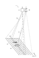
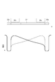
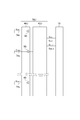
- FIG. 1 is a diagram for explaining an irradiation region of a light source.
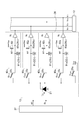
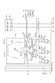
- FIG. 2 is a diagram showing a connection configuration between the pixel array and peripheral circuits.
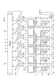
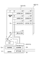
- FIG. 3 is a block diagram showing a schematic configuration of the distance image sensor 10 according to the first embodiment.
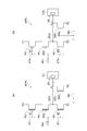
- FIG. 4 is a timing chart for explaining the principle of distance calculation using the distance image sensor 10 of FIG.
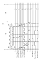
- FIG. 5 is a block diagram showing a detailed configuration of the distance image sensor 10 of FIG.
- Figure 6 is a diagram showing a detailed circuit configuration of a NOR type driver circuit 41 1 in Fig.
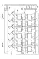
- Figure 7 is a circuit diagram showing a connection state between combined capacitance C G of Figure NOR type driver circuit 41 1 of 5, 41 2, 41 3, 41 4 and NAND-type driver circuit 41 5 and the pixel circuit 13.
- FIG. 8 is a circuit diagram showing a read circuit.
- FIG. 9 is a timing chart showing the operation of the light source and the operation of the pixel array.
- FIG. 10 is a diagram for explaining the operation of the light source and the operation of the pixel array.
- FIG. 11 is a block diagram showing a detailed configuration of the distance image sensor according to the second embodiment. 12
- the control pulse G 1p generated in the distance image sensor 10A is a diagram showing a waveform and a NOR-type driver circuit 41 1 of the output signal G 1out of the waveform of the inverted signal of the G 1n.
- FIG. 13 is a diagram showing a time waveform of a through current I with respect to an input control pulse VIN when a general CMOS inverter circuit is used.
- FIG. 13 is a diagram showing a time waveform of a through current I with respect to an input control pulse VIN when a general CMOS inverter circuit is used.
- FIG. 14 is a graph showing the relationship between the input control pulse VIN and the through current I in a general CMOS inverter circuit.
- FIG. 15 is a block diagram showing a detailed configuration of the distance image sensor according to the third embodiment.
- FIG. 16 is a diagram showing an example of waveforms of transfer control pulses G 1out and G 2out generated by the distance image sensor 10B.
- FIG. 17 is a plan view showing an arrangement example of each region in the signal charge processing region 17 of the pixel circuit 13.
- FIG. 18 is a diagram showing a potential distribution in the signal charge processing region 17 of the pixel circuit 13.
- FIG. 19 is a block diagram showing a detailed configuration of the distance image sensor according to the fourth embodiment.
- FIG. 20 is a block diagram showing a detailed configuration of the distance image sensor according to the fifth embodiment.
- FIG. 21 is a block diagram showing a detailed configuration of the distance image sensor according to the sixth embodiment.
- FIG. 22 is a diagram for explaining an irradiation region of the light source of the seventh embodiment.
- FIG. 23 is a diagram showing a connection configuration between the pixel array of the seventh embodiment and peripheral circuits.
- FIG. 24 is a block diagram showing a detailed configuration of the distance image sensor according to the seventh embodiment.
- FIG. 25 is a block diagram showing a schematic configuration of the distance image sensor according to the eighth embodiment.
- FIG. 26 is a block diagram showing a detailed configuration of the distance image sensor according to the eighth embodiment.
- FIG. 27 is a circuit diagram showing a detailed configuration of a drive circuit included in the distance image sensor according to the eighth embodiment.
- FIG. 28 is a circuit diagram showing a detailed configuration of a row scan pattern generation circuit.
- FIG. 29 is a timing chart relating to the row scan pattern generation circuit shown in FIG. 28.
- FIG. 30 is a diagram showing a detailed configuration of a pixel circuit included in the distance image sensor according to the eighth embodiment.
- FIG. 31 is a diagram showing a potential distribution with respect to the pixel circuit of FIG. 30.
- FIG. 32 is a block diagram showing a detailed configuration of the distance image sensor according to the ninth embodiment.
- FIG. 33 is a circuit diagram showing a detailed configuration of a pixel switching circuit included in the distance image sensor of the ninth embodiment.
- FIG. 34 is a diagram showing a detailed configuration of a pixel circuit included in the distance image sensor according to the ninth embodiment.
- FIG. 35 is a block diagram showing a detailed configuration of the distance image sensor according to the tenth embodiment.
- FIG. 36 is a circuit diagram showing a detailed configuration of a drive circuit included in the distance image sensor according to the tenth embodiment.
- FIG. 37 is a diagram showing a detailed configuration of a pixel circuit included in the distance image sensor according to the tenth embodiment.
- FIG. 38 is a timing chart showing the operation of the light source and the operation of the pixel array as the first modification.
- FIG. 39 is a timing chart showing the operation of the light source and the operation of the pixel array as the second modification.
- FIG. 40 is a timing chart showing the operation of the light source and the operation of the pixel array as the third modification.
- FIG. 41 is a timing chart showing the operation of the light source and the operation of the pixel array as the fourth modification.
- FIG. 42 is a diagram showing a detailed configuration of a pixel circuit included in the distance image sensor according to the fifth modification.
- FIG. 43 is a diagram showing a potential distribution with respect to the pixel circuit of FIG. 42.
- FIG. 44A is a diagram showing a NOR type driver circuit according to a sixth modification.
- FIG. 44B is a diagram showing a NOR type driver circuit according to a seventh modification.
- FIG. 45A is a diagram showing a NOR type driver circuit according to the eighth modification.
- FIG. 45B is a diagram showing a NOR type driver circuit according to a ninth modification.
- FIG. 46A is a diagram showing a NAND type driver circuit according to a tenth modification.
- FIG. 46B is a diagram showing a NAND driver circuit according to the eleventh modification.
- FIG. 47A is a diagram showing a NAND driver circuit according to a twelfth modification.
- FIG. 47B is a diagram showing a NAND driver circuit according to the thirteenth modification.
- FIG. 48 is a diagram showing a pixel circuit included in the distance image acquisition device of the 14th modification.
- Figure 49 is a diagram showing a control pulse input to the pixel circuit 13 1.
- FIG. 50 is a diagram showing another pixel circuit included in the distance image acquisition device of the 14th modification.
- FIG. 51 is a diagram showing a pixel circuit included in the distance image acquisition device of the fifteenth modification.
- FIG. 52 is a diagram showing another pixel circuit included in the distance image acquisition device of the fifteenth modification.
- FIG. 53 is a timing chart showing the operation of the distance image acquisition device of the fifteenth modification.
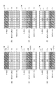
- FIG. 54A is a diagram showing a felt pixel region and a dead pixel region in the first operation mode of the eleventh embodiment.
- FIG. 54B is a diagram showing a felt pixel region and a dead pixel region in the second operation mode.
- FIG. 54 (c) is a diagram showing a felt pixel region and a dead pixel region in the third operation mode.
- FIG. 55 is a timing chart showing the operation of the light source and the operation of the pixel array according to the eleventh embodiment.
- FIG. 56 is a diagram showing a connection configuration between the pixel array of the 16th modification and the peripheral circuit.
- the distance image acquisition device 1 has a line scan light source and performs a felt / insensitive pixel scan function. With these components and functions, the distance image acquisition device 1 generates a distance image based on the flight time method. The distance image includes distance information for each pixel.
- the distance image acquisition device 1 has a light source 11 and a distance image sensor 10.
- the light source 11 is composed of, for example, a semiconductor light emitting element such as a light emitting diode or a laser diode and a drive circuit for driving the semiconductor light emitting element.
- a semiconductor light emitting element such as a light emitting diode or a laser diode
- a drive circuit for driving the semiconductor light emitting element As the light source 11, an element that generates light in a wavelength region such as a near infrared region or a visible light region can be used.
- the light source 11 is a line scan light source.
- Light source 11 projects a strip-shaped pulse light L P having a line (linear) or width and having a periodicity in the measurement target region A. Pulse light L P along the direction (Y direction) intersecting the direction (X direction) of extension of the irradiation region R, to scan the measurement area A one-dimensionally.
- the light source 11 irradiates pulsed light L P toward the measurement target region A including the object S.
- Pulse light L P to the light source 11 is emitted has a two-dimensionally spread.
- its aspect ratio is relatively large.
- the horizontal direction (X direction) of the irradiation area R is extremely large with respect to the vertical direction (Y direction) of the irradiation area R.
- the light source 11 may be a line light source that irradiates substantially one-dimensional (linear) light.
- pulse light L P would be irradiated to a portion of the measurement target region A. Therefore, the light source 11 changes the irradiation position of the pulse light L P every time in the measurement target region A.
- Pulse light L P is reflected in the object S.
- the reflected light is incident on the distance image sensor 10. That is, the reflected light is the incident pulse light LR (return light).
- the distance image sensor 10 is an image sensor having a two-dimensional pixel array 14 that receives the reflected light from the measurement target area A.
- Pixel array 14 includes a plurality of pixel circuits 13 arranged two-dimensionally to receive the incident pulse light L R. The detailed configuration of the pixel circuit 13 will be described in detail in a later paragraph.
- the distance image sensor 10 includes a plurality of pixel circuits (plurality of pixel circuit units) 13.
- a plurality of pixel circuits 13, the two-dimensional direction (for example, column and row directions) incident pulses are arranged in a two-dimensional array to constitute an image sensor, pulse light L P has occurred is reflected by the object S generating a detection signal by photoelectrically converting the light L R.
- the distance image sensor 10 is used together with the light source 11 and the calculation circuit 12 for generating the distance image.
- Range image sensor 10 in synchronization with the scanning of the pulsed light L P from the light source 11, incident pulse light L R due to the pulsed light L P has to scan the pixel area to be incident. This operation is controlled by the control pulses provided by the arithmetic circuit 12 and the peripheral circuits 31.
- the arithmetic circuit 12 may be configured by a dedicated integrated circuit such as a one-chip microcomputer including a CPU, RAM, ROM, an input / output device, and the like, or may be configured by a general-purpose computer such as a personal computer.
- the calculation circuit 12 is electrically connected to the distance image sensor 10 and the light source 11, and uses the detection signals generated by the plurality of pixel circuits 13 to calculate the distance information regarding the object S for each pixel, and for each pixel. Generates and outputs a distance image including two-dimensional image information that reflects the distance information. This function is performed by the signal processing unit 12c of the arithmetic circuit 12.
- the arithmetic circuit 12 also has a light source control unit 12a for controlling the irradiation timing of the pulsed light L P by the light source 11. Further, the arithmetic circuit 12 also has a pixel control unit 12b for driving the pixel circuit 13.
- the arithmetic circuit 12 is connected to the peripheral circuit 31.
- the arithmetic circuit 12 gives a control signal to the peripheral circuit 31.
- the peripheral circuit 31 provides a control signal to the pixel array 14.
- Control signal comprises control pulses G 1 ⁇ G 4, G D , logic pulse E SR (j), at least one of these inverted signals. Further, the control signal, control pulses G 1 ⁇ G 4, G D , logic pulse E SR (j), the transfer control pulse G 1out ⁇ G 4out generated by a pulse selected from these inverted signals, the G Dout include.
- the peripheral circuit 31 includes a distribution circuit 33, a pixel switching circuit 34, and a read control circuit 27.
- the distribution circuit 33 and the pixel switching circuit 34 set the sensitivity of the pixel circuit 13 to be felt / insensitive in units of a plurality of lines (one line or more).
- the read control circuit 27 is a scanning circuit that reads a signal in units of several lines (one line or more). The meanings of "pixel sensitivity", “make the pixel sensitive”, and “make the pixel insensitive” will be described in detail later.
- the distribution circuit 33 is electrically connected to the pixel array 14 and provides control pulses G 1 to G 4 and G D for the plurality of pixel circuits 13.
- the pixel switching circuit 34 is electrically connected to the pixel array 14 and provides logic pulses to the plurality of pixel circuits 13.
- the distribution circuit 33 and the pixel switching circuit 34 set the sensitivity of the pixel circuit 13 to be felt or insensitive in units of one or more rows. That is, the distribution circuit 33 and the pixel switching circuit 34 are pixel-sensitive / insensitive scanning circuits.
- the distribution circuit 33 and the pixel switching circuit 34 cooperate with the light source control unit 12a to position the irradiation region R, the sensitive pixel region AE (sensitive region), and the dead pixel region AN (dead region). Synchronize in time. This control is executed a plurality of times within one frame.
- the read control circuit 27 is electrically connected to the pixel array 14 and provides control pulses for the read operation to the plurality of pixel circuits 13.
- the read control circuit 27 provides a control pulse for reading a signal from the pixel circuit 13 in units of one or more lines equal to the range of the felt pixel region AE described later. That is, the read control circuit 27 is a read scanning circuit.
- the pixel circuit 13 includes a photoelectric conversion region 21 composed of semiconductor elements and having a function of converting incident pulsed light LR into electric charges, and first to first ones provided close to the photoelectric conversion region 21 and separated from each other. and 4 of the charge read area 22 1 to 22 4 and the charge discharging region 23, provided corresponding to each of the first to fourth charge read area 22 1 to 22 4 and the charge discharging region 23, from the photoelectric conversion region 21 a first to fourth control electrode 25 1 to 25 4 and the fifth control electrode 25 D of for applying a transfer control pulse for charge transfer between the respective areas, first to fourth charge includes a voltage detecting means 26 1 to 26 4 for reading a detection signal from each of the read area 22 1 to 22 4.
- Voltage detecting means 26 1 to 26 4 is, for example, an amplifier comprising a source follower amplifier. Voltage detecting means 26 1 to 26 4, the control of the arithmetic circuit 12, detects and amplifies the voltage with respect to a reference potential of selectively each charge read area 22 1 to 22 4. Voltage detecting means 26 1 to 26 4 outputs to the arithmetic circuit 12 the amplified voltage as a detection signal.
- the pixel circuit 13 has a configuration that makes the pixel circuit 13 insensitive to light by eliminating the sensitivity of the pixels.
- the light mentioned here including pulse light L incident pulse light due to P L R and background light not due to pulse light L P.
- the "eliminate the sensitivity of pixels” and “insensitive to the incident pulse light L R” refers to a state that no electric charge generated in the photoelectric conversion region 21 are read out to the charge read area 22 1 to 22 4.
- the "eliminate the sensitivity of the pixel” and “insensitive to the incident pulse light L R” refers to a state of moving the charge generated in the photoelectric conversion region 21 to the charge discharging region 23.
- "eliminate the sensitivity of the pixel” is configured to "insensitive to the incident pulse light L R" configuration and a control electrode 25 D is a charge discharging region 23 and the drain gate is the drain.
- the pixel circuit 13 is formed on a p-type semiconductor substrate such as a silicon substrate. That is, the photoelectric conversion region 21 is a pixel composed of an active region forming layer made of a p-type semiconductor, an n-type surface embedded region, a p-type pinning layer, and an insulating film, which are sequentially formed on a p-type semiconductor substrate. It is provided in the center of the cambium. Then, n-type charge read area 22 1 to 22 4 and the charge discharging region 23 of high impurity concentration than the active region formed layer at a position separated from each other as close to the photoelectric conversion region 21 are formed.
- control electrode 25 1 ⁇ 25 4, 25 D are provided on each of the charge transfer path to each of the charge read area 22 1 to 22 4 and the charge discharging region 23 from the photoelectric conversion region 21 on the insulating film.
- the control electrodes 25 1 to 25 4 and 25 D may be provided on the charge transfer path, respectively.
- the control electrodes 25 1 to 25 4 , 25 D may be separately provided in a plurality of electrode portions so as to sandwich the charge transfer path from both sides.
- the transfer control pulse is applied to the phase different from each other.
- the depletion potential of the surface-embedded region changes sequentially.
- a potential gradient is sequentially formed such that the charge is transported to one of the charge transfer paths.
- a number generated on the surface buried region of the photoelectric conversion region 21 carrier (charge) is moved to one of the charge read area 22 1 to 22 4 and the charge discharging region 23.
- Arithmetic circuit 12 emission timing of the pulsed light L P by the light source 11 to control the intensity of the pulse light L P, and the pulse width of the pulse light L P.
- the pulse light L P of a predetermined duration T 0, repeatedly controlled to occur within a period of 1 frame is a repetition period of the preset distance calculation (light source control unit 12a).
- the arithmetic circuit 12 transfers the electric charge generated in the photoelectric conversion region 21 to the charge discharge region 23 via the peripheral circuit 31 of the distance image sensor 10 before the application timing of these transfer control pulses.
- a control pulse is applied to the control electrode 25 D.
- Light source control unit 12a of the arithmetic circuit 12 controls the light source 11, pulsed light L P is irradiated to a portion of the measurement target region A. That is, pulse light L P is not irradiated collectively for the entire region of the measurement target region A.
- the irradiation region R of the pulse light L P is a region of rectangular shape extending in the width direction X of the measurement target region A. The width of the irradiation region R may coincide with the width of the measurement target region A. Then, the irradiation region R is set so as to be aligned in the height direction (Y direction) of the measurement target region A.
- Arithmetic circuit 12 controls the position of the irradiation region R of the pulse light L P emitted from the light source 11. Arithmetic circuit 12 controls the light source 11, and sets a certain area as an irradiation region R, is irradiated with pulsed light L P to the region. Arithmetic circuit 12, the irradiation region R to sequentially move downward, is irradiated with pulsed light L P by controlling the light source 11.
- Order to irradiate the pulsed light L P is not limited to the embodiments described above. As described above, instead of the mode of irradiating in order from top to bottom, the order of irradiating in order from bottom to top may be used. Moreover, in the mode of irradiating from the top to the bottom, the mode of irradiating every other may be used.
- the arithmetic circuit 12 repeatedly executes the calculation of the distance for each pixel circuit 13 for each of a plurality of frames, and repeatedly generates a distance image including the distance information obtained as a result (signal processing unit 12c). That is, the arithmetic circuit 12, based on the detection signal outputted from the voltage detecting means 26 1 to 26 4 of the pixel circuit 13, calculates the distance information. Then, the arithmetic circuit 12 generates a distance image including the distance information corresponding to each pixel circuit 13 and outputs the distance image to the external device. Examples of the output destination external device include an output device such as a display device and a communication interface device.
- FIG. 4 is a timing chart for explaining the principle of distance calculation by the arithmetic circuit 12.
- FIG. 4 shows the timing of various signals controlled by the arithmetic circuit 12 and the timing of charge accumulation in each region of the pixel circuit 13.
- Figure 4 is from top to bottom, emission timing of the pulsed light L P, the control electrodes 25 1 to 25 4, 25 application timing of the transfer control pulse applied to the D, the first to fourth charge read area 22 1 to 22 The charge accumulation timing in No. 4 is shown.
- the transfer control pulse duration T 0 is applied continuously so as not to overlap each other to the control electrode 25 1 ⁇ 25 4, 25 D NS.
- incident pulse light L R is the electric charge generated in the photoelectric conversion region 21 by being photoelectrically converted, corresponding to the delay time T D with respect to pulse light L P of the incident pulse light L R, 2 one charge read area 22 2, 22 3, or the two charge read area 22 3, is distributed to 22 4.
- the charge read area 22 only the charge in the charge quantity N B due to noise such as background light and dark current in the time window defined by the transfer control pulse of the control electrode 25 1 is transported.
- the arrival timing of the incident pulse light L R is defined by the two transfer control pulses of the control electrode 25 3, 25 4, the charge amount of the charge readout area 22 3 charge charge amount N sm1 distributed in correspondence with the delay time T D to N B has been added is transported.
- the charge readout area 22 4 the charge amount of charges N sm2 distributed in correspondence with the delay time T D to the amount of charge N B has been added is transported.
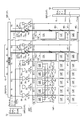
- FIG. 5 is a block diagram showing a detailed configuration of the distance image sensor 10. Note that FIG. 5 shows a part of the pixel circuit 13 of the distance image sensor 10, and the circuit configuration of the main part is shown.
- the distance image sensor 10 includes a plurality of pixel circuits 13 arranged in a two-dimensional array, and peripheral circuits 31 arranged in a peripheral portion of the pixel circuits 13.
- the peripheral circuit 31 is provided in the peripheral portion of the arrangement area of the plurality of pixel circuits 13 on the same semiconductor substrate as the pixel circuit 13.
- the peripheral circuit 31 distributes the control pulses G 1 , G 2 , G 3 , G 4 , and G D for the control electrodes 25 1 , 25 2 , 25 3 , 25 4 , and 25 D applied from the arithmetic circuit 12.
- a circuit 33 respective control pulses G 1 output from the distribution circuit 33, G 2, G 3, G 4, G inverter circuit 35 1 D inversion and shaping to the output, 35 2, 35 3, 35 4 , including a 35 5, the.
- the inverter circuit 35 1, 35 2, 35 3, 35 4, 35 5, constitute the inverter circuit unit 38.
- a pair of inverter circuits 35 1, 35 2, 35 3, 35 4, 35 5, respectively, corresponding to the number of the control electrodes 25 1, 25 2, 25 3 , 25 4, 25 D included in each pixel circuit 13 It is repeatedly provided in the row direction for each pixel circuit group 15 including the pixel circuits 13 adjacent to each other in the row direction (horizontal direction in FIG. 5). Then, the control electrodes 25 1, 25 2, 25 3, 25 4, 25 inverter circuit 35 1 of the number corresponding to the number of D, 35 2, 35 3, 35 4, 35 5, respectively, in the pixel circuit group 15 They are arranged side by side in the row direction (X direction) so as to be located in the peripheral portion between two adjacent pixel circuits 13.
- CMOS Complementary MOS
- CMOS Complementary MOS
- the drain of the p-type MOS transistor 37 and the drain of the n-type MOS transistor 39 are connected to each other.
- the source of the p-type MOS transistor 37 is connected to the high potential line VDH.
- the source of the n-type MOS transistor 39 is connected to the low potential line VDL.
- the gate of the p-type MOS transistor 37 and the gate of the n-type MOS transistor 39 are connected as input terminals to the outputs of the control pulses G 1 , G 2 , G 3 , G 4 , and G D of the distribution circuit 33 in common.
- NS The connection point between the drain of the p-type MOS transistor 37 the drain and n-type MOS transistor 39, respectively of the inverter circuit 35 1, 35 2, 35 3, 35 4, 35 as a fifth output terminal, the pixel circuit group 15 Connected to.
- each of the inverter circuits 35 1, 35 2, 35 3, the inverted signal of 35 4, 35 control pulses G 1 to the pixel circuit group 15 from 5, G 2, G 3, G 4, G D is output ..
- the peripheral circuit 31 includes a pixel switching circuit 34.
- the pixel switching circuit 34 switches between the feeling and the feeling of the pixel circuit 13.
- the pixel circuit 13 is the sensitive, refers to storage ready charge in a charge read area 22 1 to 22 4. More specifically, the sensible, it is able to pass the charge from the photoelectric conversion region 21 to one of the charge read area 22 1 to 22 4. In other words, sensation is a state in which charges are not transferred from the photoelectric conversion region 21 to the charge discharge region 23, which is a drain.
- the pixel circuit 13 is insensitive, refers to a state that does not accumulate charges in the charge read area 22 1 to 22 4. More specifically, insensitivity is a state in which charges are not transferred from the photoelectric conversion region 21 to any of the charge reading regions 22. In other words, insensitivity is a state in which charges are transferred from the photoelectric conversion region 21 to the charge discharge region 23, which is a drain.
- the pixel switching circuit 34 outputs the logic pulse E SR (j) and the inverted signal of the logic pulse E SR (j).
- Inverted signal of the logic pulse E SR (j) switches the permission / prohibition of the charge transfer from the photoelectric conversion region 21 into one of the charge read area 22 1 to 22 4.
- the logic pulse ESR (j) switches permission / prohibition of charge transfer from the photoelectric conversion region 21 to the charge discharge region 23.
- the inverted signal of the logic pulse E SR (j) ⁇ H> Write as.
- the logical pulse E SR (j) that allows charge transfer from the photoelectric conversion region 21 to the charge discharge region 23 is described as the logical pulse E SR (j) ⁇ H>.
- the logic pulse E SR (j) that prohibits charge transfer from the photoelectric conversion region 21 to the charge discharge region 23 is described as the logic pulse E SR (j) ⁇ L>.
- the letters "H" and "L” in parentheses are for convenience of explanation only.
- the pixel switching circuit 34 gives an inverted signal of the logic pulse E SR (j), which is a pixel drive pulse, and a logic pulse E SR (j ) to the pixel circuit 13 from the horizontal direction (X direction). That is, the pixel switching circuit 34 provides the pixel circuit 13 via the wiring 48 G, 48 D of the inverted signal and the logic pulse E SR a (j) extending in the horizontal direction of the logic pulse E SR (j). As a result, the pixel switching circuit 34 collectively sets the pixel circuit 13 to be sensational for each row. Further, the pixel switching circuit 34 collectively sets the pixel circuit 13 for each row in a non-sensing manner.
- the pixel switching circuit 34 when the pixel circuits 13 included in the predetermined line are collectively set to be sensational, the pixel switching circuit 34 outputs the inversion signal ⁇ H> of the logic pulse ESR (j) to the wiring 48 G. outputs a logic pulse E SR (j) ⁇ L> to the wiring 48 D while. Also, when setting the insensitive collectively pixel circuit 13 included in the given row, the pixel switching circuit 34, the inverted signal line and outputs the ⁇ L> of logic pulse E SR (j) to the wiring 48 G 48 The logic pulse E SR (j) ⁇ H> is output to D.
- the pixel array 14 has a plurality of pixel circuits 13 two-dimensionally arranged in N rows and M columns.
- the pixel switching circuit 34 sets all the pixel circuits 13 included in the jth row and the j + 1th row to be sensational.
- the region having the pixel circuit 13 set to be felt is called a felt pixel region AE.
- a sensitive pixel region AE are sensible area to be incident pulse light L R is the return light.
- the pixel switching circuit 34 sets all the pixel circuits 13 included in the first to (j-1) rows and the first to (j + 2) to Nth rows insensitively.
- the region having the pixel circuit 13 set to be insensitive is referred to as an insensitive pixel region AN.
- the dead pixel region AN is a dead region that does not accumulate charges according to the incident light.
- the pixel switching circuit 34 sets the pixel circuits 13 included in two rows adjacent to each other to be sensational, and sets the pixel circuits 13 included in the other rows to be insensitive.
- the number of rows that make up the felt pixel area AE is not limited to two.
- the number of rows constituting the felt pixel region AE may be 1, or may be 3 or more.
- the felt pixel area AE corresponds to the irradiation area R.
- the arithmetic circuit 12 sets an area of the pixel array 14 that is previously correlated with the irradiation region R in Yukan pixel region AE.
- NOR-type driver circuit 411 included in a separate pixel circuits 13 constituting one pixel circuit groups 15, 41 2, 41 3, 41 4, the control electrode 25 1 included in each pixel circuit 13, 25 2, 25 3, in the number corresponding to 25 4 of number, are repeatedly provided for each pixel circuit group 15 in the row direction.
- control electrodes 25 1, 25 2, 25 3 , 25 4, 25 D NOR type driver circuit 41 1 of the number corresponding to the number of, 41 2, 41 3, 41 4, respectively, of the peripheral circuit 31 inverter corresponding to the circuit 35 1, 35 2, 35 3, 35 4 are arranged in the row direction.
- the NAND-type driver circuit 41 5 of the number corresponding to the number of the control electrode 25 D, respectively, are arranged corresponding to the inverter circuit 35 5 of the peripheral circuit 31.
- NOR-type driver circuit 41 1, 41 2, 41 3, 41 4 and NAND-type driver circuit 41 5 is a CMOS driver circuit.
- Pixel circuits 13 1-13 4 each has a NOR type driver circuits 41 1-41 4.
- NOR-type driver circuits 41 1-41 4 each, p-type MOS transistors 43 1, 43 2, 43 3, 43 4 and the p-type MOS transistors, 44 2, 44 3, 44 4 and n-type MOS transistors 45 1, 45 and a 2, 45 3, 45 4.
- Pixel circuits 13 5 has a NAND-type driver circuit 41 5.
- NOR-type driver circuits 41 1-41 4 has the following configuration.
- the source of the p-type MOS transistors 43 1-43 4 is connected to the high potential line V DH.
- the gate of the p-type MOS transistors 43 1-43 4 is an input terminal.
- the gate of the p-type MOS transistors 43 1-43 4 are connected via a wire 47 1-47 4 to the output of the inverter circuits 35 1 to 35 4.
- the drain of the p-type MOS transistors 43 1-43 4 is connected to the source of p-type MOS transistors 44 1-44 4.
- the source of the p-type MOS transistors 44 1-44 4 is connected to the drain of the p-type MOS transistors 43 1-43 4.
- the gate of the p-type MOS transistors 44 1-44 4 is an input terminal.
- the gate of the p-type MOS transistors 44 1-44 4 is connected to the pixel switching circuit 34 through the wiring 48 G.
- p-type MOS transistors 44 1-44 4 drains of n-type MOS transistors 45 1 to 45 4 are connected to each other.
- the drain of the p-type MOS transistors 44 1-44 4 of the drain and n-type MOS transistors 45 1 to 45 4 are connected to the control electrodes 25 1 to 25 4.
- the source of the n-type MOS transistors 45 1 to 45 4 are connected to the drain of the p-type MOS transistors 44 1-44 4.
- the gate of the n-type MOS transistors 45 1 to 45 4 are input terminals.
- the gate of the n-type MOS transistors 45 1 to 45 4 are connected via a wire 47 1-47 4 to the output of the inverter circuits 35 1 to 35 5.
- the p-type MOS transistors 43 1-43 4 the gate and n-type MOS transistors 45 1 to 45 4 of the gate is common to each other.
- the source of the n-type MOS transistors 45 1 to 45 4 are connected to the low potential line V DL.
- NAND-type driver circuit 41 5 has the following configuration.
- the source of the p-type MOS transistor 43 5 is connected to the high potential line V DH.
- the gate of the p-type MOS transistor 43 5 is an input terminal.
- the gate of the p-type MOS transistor 43 5 is connected via a wire 47 5 to the output of the inverter circuit 35 5.
- the drain of the p-type MOS transistor 43 5 of the drain and n-type MOS transistor 46 are connected to each other.
- the source of the n-type MOS transistor 46 is connected to the drain of the p-type MOS transistor 43 5.
- the gate of the n-type MOS transistor 46 is an input terminal.
- the gate of the n-type MOS transistor 46 is connected to the pixel switching circuit 34 through the wiring 48 D.
- the source of the n-type MOS transistor 46 is connected to the drain of the n-type MOS transistor 45 5.
- the source of the n-type MOS transistor 45 5 is connected to the drain of the n-type MOS transistor 46.
- the gate of the n-type MOS transistor 45 5 is an input terminal.
- the gate of the n-type MOS transistor 45 5 is connected via a wire 47 5 to the output of the inverter circuit 35 5.
- the p-type MOS transistor 43 5 gates and n-type MOS transistor 45 5 gates are common to each other.
- the source of the n-type MOS transistor 45 5 is connected to the low potential line V DL.
- each of the NOR type driver circuit 41 1, 41 2, 41 3, 41 4 and NAND-type driver circuit 41 5 from the control electrode 25 1, 25 2, 25 3, 25 4, transfer control to 25 D Pulses G 1out to G 4out and G Dout can be output.
- Transfer control pulse G 1out, G 2out, G 3out , G 4out, G Dout has a signal and insensitive to the inverted signal and the sensitive pixel circuit 13 by a logic pulse E SR (j) of the logic pulse E SR (j) It is controlled by the signal to be used.
- connection to the input of the NOR type driver circuit 41 1, 41 2, 41 3, 41 4 and NAND-type driver circuit 41 5, and the output of the inverter circuit 35 1, 35 2, 35 3, 35 4, 35 5, the wiring 47 1, 47 2, 47 3, 47 4, 47 5 are provided one by one in the gap portion between the two pixel circuits 13 adjacent to each other of the pixel circuit group 15. Further, the output terminal of the NOR type driver circuit 41 1 provided for each pixel circuit group 15, the control electrode 25 1 of the all pixel circuits 13 included in the pixel circuit group 15, a NOR driver circuit 41 1 is provided that It is connected via the wiring 49 in the pixel circuit 13 and the wiring 51 extending across all the pixel circuits 13 included in the pixel circuit group 15.
- each of the output terminals of the NOR type driver circuit 41 2, 41 3, 41 4 and NAND-type driver circuit 41 5 each of the control electrodes 25 2 of all pixel circuits 13 included in the pixel circuit group 15, 25 It is connected to 3 , 25, 4 , 25 D via two wires.
- the inverter circuit 35 1 and the NOR type driver circuit 41 1 of the above structure, the first control electrode driver circuit for applying a transfer control pulse G 1out to the control electrode 25 1 of the pixel circuits 13 constituting the pixel circuit group 15 is configured Will be done.
- the inverter circuit 35 2, 35 3, 35 4, 35 5 and NOR-type by each of the driver circuits 41 2, 41 3, 41 4 and NAND-type driver circuit 41 5, a pixel circuit constituting the pixel circuit group 15 the control electrode 25 and second 13, 25 3, 25 4, transferred to 25 D control pulse G 2out, G 3out, G 4out , the control electrode driver circuit of the second to fifth applying a G Dout is formed.
- wirings 48 G and 48 D are connected to the pixel switching circuit 34 of the peripheral circuit 31.
- Wiring 48 G and 48 D extend in the row direction.
- the row direction means the horizontal direction with respect to the paper surface.
- the wiring 48 G, 48 D extends along a direction lined with the pixel circuits 13 1-13 5.
- the wiring 48 G is connected to the pixel circuits 13 1-13 4 arranged in the row direction.
- the wiring 48 D is connected to the pixel circuit 13 5.
- FIG. 6 shows a detailed circuit configuration of a NOR type driver circuit 41 1.
- NOR-type driver circuit 411 includes a capacitance component 53 formed between the p-type MOS transistor 43 1 source and n-type MOS transistor 45 1 of the source.
- the capacitance component 53 can be realized, for example, by a MOS transistor formed on the same semiconductor substrate as the pixel circuit 13. One end of the capacitance component 53 is connected to a substrate potential having a low potential, and the other end is connected to a high potential.
- the capacitance component 53 has a combined capacitance C G or capacitance of the control electrode 25 1 of the pixel circuit 13 connected to the output of the NOR type driver circuit 41 1.
- the capacitance component 53 preferably has a capacitance of 4 times or more.
- NOR-type driver circuit 41 2, 41 3, 41 4 and NAND-type driver circuit 41 5 is also a capacitance component 53.
- These NOR-type driver circuit 41 2, 41 3, 41 4 and capacitance component 53 of the NAND type driver circuit 41 5, connected to the output of a NOR-type driver circuit 41 2, 41 3, 41 4 and NAND-type driver circuit 41 5 having a respective control electrodes 25 2, 25 3 of the pixel circuit 13 is, 25 4, 25 combined capacitance C G or more capacitance D.
- the capacitance of the capacitance component 53 is preferably at least 4 times the combined capacitance C G.
- Figure 7 is, NOR type driver circuit 41 1, 41 2, 41 3, 41 NOR-type driver circuit 411 during operation of the 4, 41 2, 41 3, 41 4 and the combined capacitance C G of the pixel circuit 13 Indicates the connection status.
- (A) section shows the transfer control pulse G 1out, G 2out, G 3out , the connection state when ON G 4out (high potential).
- (B) section shows the transfer control pulse G 1out, G 2out, G 3out , the connection state when G 4out off (low potential). The same applies to the NAND driver circuit 41 5.
- the transfer control pulse G 1out, G 2out, G 3out , G 4out, during on the G Dout is capacitance component 53 is connected to both ends of the combined capacitance C G.
- the transfer control pulse G 1out, G 2out, G 3out , G 4out, G off when the charge control electrodes 25 1 which has been charged in the capacitance component 53 of Dout, 25 2, 25 3, in 25 4, 25 D Supplied towards. Therefore, the potentials of the control electrodes 25 1 , 25 2 , 25 3 , 25 4 , 25 D can be quickly raised.
- the transfer control pulse G 1out, G 2out, G 3out , G 4out, 50% of the charge required to launch to the high potential of the G Dout It can be supplied from the capacitance component 53.
- the transfer control pulse G 1out, G 2out, G 3out , G 4out, 80% of the needed to launch to the high potential of the G outD Charges can be supplied from the capacitance component 53.
- the transfer control pulse G 1out, G 2out, G 3out , G 4out, during off G Dout is at both ends of the combined capacitance C G are short-circuited.
- the potentials of the control electrodes 25 1 , 25 2 , 25 3 , 25 4 , 25 D can be quickly lowered.
- Figure 8 shows a configuration of a read circuit 80 1, 80 2, 80 3, 80 4 included in the pixel circuit 13.
- Read circuits 80 1 to 80 4 has a capacitance component 81 1-81 4, the MOS transistors 82 1-82 4, an amplifier circuit 83 1-83 4. Input of the read circuits 80 1 to 80 4 are respectively connected to the photoelectric conversion region 21. The output of the read circuit 80 1 to 80 4 are connected to the arithmetic circuit 12 through the wiring 28.
- Capacitance components 81 1-81 4 accumulates charges photoelectric conversion region 21 has occurred. Capacitance components 81 1-81 4 correspond to the charge readout area 22 1 to 22 4 shown in FIG. One end of the capacitance component 81 1-81 4 is connected to the control electrode 25 1 ⁇ 25 4, MOS transistors 82 1-82 4 and the amplifier circuit 83 1-83 4. The other end of the capacitance component 81 1-81 4 is connected to a reference potential.
- MOS transistors 82 1-82 4 discharges the charge remaining on the capacitance component 81 1-81 4.
- the source of the MOS transistor 82 1-82 4 is connected to one end of the capacitance component 81 1-81 4.
- the gate of the MOS transistor 82 1-82 4 is connected to the read control circuit 27 receives the reset pulse RT from read control circuit 27.
- the drain of the MOS transistor 82 1-82 4 is connected to a reset potential line V DR.
- Amplifier circuits 83 1-83 4 generates a voltage V O1 ⁇ V O4 corresponding to the charge accumulated in the capacitance component 81 1-81 4, and outputs the voltage V O1 ⁇ V O4 wiring 28.
- Amplifier circuits 83 1-83 4 correspond to the voltage detecting means 26 1 to 26 4 shown in FIG.
- Input of the amplifier circuit 83 1-83 4 is connected to one end of the capacitance component 81 1-81 4.
- the output of the amplifier circuit 83 1-83 4 is connected to the wiring 28.
- the amplifier circuits 83 1-83 4 is connected to the read control circuit 27 receives the read control pulse SL from the read control circuit 27.
- Amplifier circuits 83 1-83 4 voltage V O1 ⁇ V O4 which has output is provided to the arithmetic circuit 12 through the wiring 28.
- Range image sensor 10 includes a driver circuit (NOR type driver circuits 41 1-41 4 and NAND-type driver circuit 41 5) inside the pixel circuit 13.
- the distance image sensor 10 gives control pulses G 1 to G 4 , G D from the vertical direction.
- Range image sensor 10 provides the inverted signal and the logic pulse E SR of switching the sensible / dead logic pulse E SR (j) a (j) in the horizontal direction.
- Range image sensor 10 performs a logical operation of the control pulse G D and logic pulse E SR (j) in the interior of the pixel circuit 13 generates a transfer control pulse G Dout.
- the distance image sensor 10 gates the control electrode 25 D , which is a drain gate, using the transfer control pulse G Dout.
- FIG. 9 shows a timing chart showing the operation of the light source 11 and a timing chart of the logical pulse ESR (j) .
- FIG. 10 schematically shows the array division regions L 1 , L 2 , and L 3 , the felt pixel region AE, and the insensitive pixel region AN.
- the sensible pixel region AE an area capable of storing any electric charge charges generated according to the incident pulse light L R read area 22 1 to 22 4.
- the dead pixel region AN a region for discharging the charges generated in accordance with the incident pulse light L R to charge discharging region 23. That is, the light incident on the dead pixel region AN is not obtained as an output.
- the pixel array 14 is vertically divided into three regions.
- the first array divided area L 1 is the first row to the (N / 3) th row.
- the second array division region L 2 is from the (N / 3 + 1) th row to the (2N / 3) th row.
- the third array divided region L 3 is from the (2N / 3 + 1) th row to the N-th row.
- the plurality of squares indicate one pixel circuit 13.
- the area with thin hatching indicates that it is a felt pixel area AE.
- the white area indicates that it is a dead pixel area AN.
- the region surrounded by the alternate long and short dash line with rough hatching indicates that the incident pulse light LR is incident on the region from the measurement target region A.
- the distance image sensor 10 can improve the noise immunity to the background light.
- amount of pulse light L P to the light source 11 is irradiated (p 0) is constant.
- the amount of light in the irradiation area R is three times the amount of light when the entire surface of the measurement target area A is irradiated (reference numeral in FIG. 9). See 3p 0 ).
- the distance image sensor 10 can increase the noise immunity to the background light.
- the relationship between the region where the emission direction of the pulse light L P toward the light source 11 to measurement area A, the incident pulse light L R returning from the measurement object region A enters may associate by any technique. For example, in when divided into three measurement target region A in the longitudinal direction, most when the light source 11 on the region is irradiated with the pulsed light L P is the array divided region L 1 to the incident pulse light L R of the pixel array 14 May be incident.
- the distance image sensor 10 has a period PE which is one exposure period and a period PR which is one reading period in the period PF which is one frame. Further, the distance image sensor 10 performs a plurality of exposure operations in the period PF of one frame. Further, the distance image sensor 10 performs one exposure operation during one feeling period.
- the operation of the distance image sensor 10 is not limited to the above operation. Other operation examples will be described later as modified examples 1 to 5.
- the exposure operation is repeated a plurality of times.
- the pixel switching circuit 34 outputs the following logic pulse ESR (j) .
- Logic pulse E SR (1) to E SR (N / 3) HIGH.
- Logical pulse E SR (N / 3 + 1) to E SR (2N / 3) LOW.
- Logic pulse E SR (2N / 3 + 1) to E SR (N) LOW.
- Period PE 1 has a period P 1a, and duration P 1b is after the period P 1a, the.
- the light source 11 is incident pulse light L R the array divided area L 1 is irradiated with pulsed light L P to be incident.
- the duty ratio of the pulse light L P may be less than 50%.
- the light source 11 stops the irradiation of the pulse light L P.
- the pixel switching circuit 34 outputs the following logic pulse ESR (j) .
- Logic pulse E SR (1) to E SR (N / 3) LOW.
- Logic pulse E SR (2N / 3 + 1) to E SR (N) LOW.
- Period PE 2 has a period P 2a, and duration P 2b is after the period P 2a, the.
- the light source 11 irradiates the pulsed light L P so that the incident pulse light LR is incident on the array division region L 2.
- the light source 11 stops the irradiation of the pulse light L P.
- the pixel switching circuit 34 outputs the following logic pulse ESR (j) .
- Logic pulse E SR (1) to E SR (N / 3) LOW.
- Logic pulse E SR (2N / 3 + 1) to E SR (N) HIGH.
- the period PE 3 has a period P 3a and a period P 3b after the period P 3a .
- the light source 11 irradiates the pulsed light L P so that the incident pulse light LR is incident on the array division region L 3.
- the light source 11 stops the irradiation of the pulse light L P.
- period PR the period during which the operations of PE 1 to PE 3 are repeated.
- the period PE is the exposure period.
- the period PR as the reading period is set.
- These period PEs and period PRs constitute one frame (or subframe).
- signals are read from all rows.
- pulse light L P from the light source 11 is not illuminated.
- the pixel switching circuit 34 outputs the following logic pulse ESR (j) .
- Logic pulse E SR (1) to E SR (N / 3) LOW.
- Logic pulse E SR (2N / 3 + 1) to E SR (N) LOW.
- the distance image sensor 10 has a strong resistance to background light and a strong resistance to artifacts caused by the movement of the imaged object due to some effects described below.
- Range image sensor 10 when the light source control unit 12a has caused the pulse light L P so that the incident pulse light L R to sensible pixel region AE incident occurred in the photoelectric conversion region 21 in the dead pixel region AN
- a logical pulse ESR (j) that moves the charge to the charge discharge region 23.
- an operation for receiving the incident pulse light L R due to the pulsed light L P irradiates pulsed light L P, it is possible to repeat the fast while moving the sensible pixel region AE.
- the speeding up and repetition of the irradiation operation and the light receiving operation are synonymous with the temporal oversampling and integration of the light charge within the frame period in the so-called distance measurement. Therefore, good measurement results can be obtained even when the object to be measured moves at high speed due to the low-pass filter effect due to oversampling and integration.
- the range image sensor 10 performs the scanning of the linear pulse light L P emitted from the light source 11, the position and exposure operation and the reading operation by synchronizing the time so as to correspond to the scanning.
- the light source control unit 12a as all the pixel circuits 13 included in the j-th row is included in the sensible pixel region AE, emits a pulse light L P from the light source 11 Perform the action to make it.
- the peripheral circuit 31 and the light source control unit 12a perform a read operation after performing an exposure operation on a plurality of felt pixel regions AE a plurality of times. That is, after the exposure operation for all the pixel circuits 13, signals are collectively read from all the pixel circuits 13. According to this operation, a signal can be read from the entire pixel array 14 after a plurality of exposure operations in the entire pixel array 14.
- the exposure operation of the range image sensor 10 of the first embodiment in a state in which the peripheral circuit 31 has provided a control pulse G 1 ⁇ G 4, G D and logic pulse E SR (j), the light source control unit 12a is pulse light L Generate P only once. This operation also makes it possible to further speed up the operation of the distance image sensor 10.
- control pulses G 1 , G 2 , G 3 , G 4 , and G D are distributed by the distribution circuit 33 provided in the peripheral circuit 31.
- a control pulse G 1, G 2, G 3 , G 4, G transfer control pulse based on D is, NOR type driver circuit provided in one pixel circuit 13 of the pixel circuits 15 41 1, 41 2 , 41 3, 41 4 and the first to fifth control electrode driver circuit composed of a NAND driver circuit 41 5, the control electrodes 25 1, 25 2 of all pixel circuits 13 constituting the pixel circuit group 15, It is applied to 25 3 , 25 4 , 25 D.
- each pixel circuit 13 the timing of charge transfer between the photoelectric conversion region 21 and the charge read area 22 1, 22 2, 22 3, 22 4 and the charge discharging region 23 is controlled. Due to the configuration in which the control pulses G 1 , G 2 , G 3 , G 4 , and G D are relayed by the first to fifth control electrode driver circuits, the waveform of the transfer control pulse can be displayed even if the number of pixels increases. Blurring can be reduced, and pixels can be driven at high speed to generate a distance image with high distance resolution.
- each of the first to fifth control electrode driver circuits is shared by the pixel circuit group 15 including the same number of pixel circuits 13 as the number of control electrodes, so that the transfer control pulse can be transmitted while keeping the pixel size small.
- the bluntness of the waveform can be reduced.
- NOR-type driver circuit 41 1, 41 2, 41 3, 41 4 and NAND-type driver circuit 41 5 is provided in a separate pixel circuits 13 of the pixel circuits 15.
- the driving of the different control pulse G 1, G 2, G 3 , G 4 to prevent cross talk between G D stable picture can be realized.
- the pixel circuit 13 has a driver circuit inside. Therefore, the gating for feeling / feeling is performed by the logical operation in the pixel circuit 13.
- each of the NOR type driver circuit 41 1, 41 2, 41 3, 41 4 and NAND-type driver circuit 41 5, including a capacitance component 53 is realized.
- the presence of capacitance component 53 can be reduced control electrodes 25 1, 25 2, 25 3, 25 4, 25 current generated in the power supply with the charging and discharging of the capacitance component of D at the time of driving the pixel circuit 13.
- the situation where the power supply voltage drops momentarily can be prevented, and the pixel (pixel circuit 13) can be driven at high speed.
- FIG. 11 is a block diagram showing a schematic configuration of the distance image sensor 10A.
- the distance image sensor 10A shown in FIG. 11 has the functions of the distribution circuit 33A, the configuration of the inverter circuit in the peripheral circuit 31A, the peripheral circuit 31A, and the pixel circuit 13A, as compared with the distance image sensor 10 according to the first embodiment. The connection configuration between them is different.
- the peripheral circuit 31A has a distribution circuit 33A, an inverter circuit unit 38A, and a pixel switching circuit 34A. Since the pixel switching circuit 34A has the same configuration and function as the pixel switching circuit 34 of the first embodiment, the description thereof will be omitted.
- the distribution circuit 33A distributes the control pulse G 1 to two control pulses G 1p and G 1n , respectively, and repeatedly generates them in the row direction. Similarly, the distribution circuit 33A distributes the control pulses G 2 , G 3 , G 4 , and G D to two control pulses G 2p , G 2n and two control pulses G 3p , G 3n , and 2 One control pulse G 4p , G 4n and two control pulses G Dp , G Dn are repeatedly generated. These two control pulses G 1p and G 1n are generated in synchronization with the on / off of the control pulse G 1 so that their on periods do not match.
- the on-period of the control pulse G 1p is generated to fit within the ON period of the control pulse G 1n.
- the two control pulses G 2p, G 2n , the two control pulses G 3p , G 3n , the two control pulses G 4p , G 4n , and the two control pulses G Dp , G Dn are the control pulses G 2 , in synchronization with the on-off of G 3, G 4, G D , is generated as the oN period of each other do not match.
- the peripheral circuit 31A, the inverter circuit 35 1 in the first embodiment, 35 2, 35 3, 35 4, 35 5 a similar configuration of the inverter circuit 61 1, 61 2, 61 3, 61 4, 61 5 and, Inverter circuits 63 1 , 63 2 , 63 3 , 63 4 , 6 3 5 are included.
- These inverter circuits 61 1, 61 2, 61 3, 61 4, 61 5, and the inverter circuits 63 1, 63 2, 63 3, 63 4, 63 5 constitute an inverter circuit unit 38A.
- One set of inverter circuits 61 1 , 61 2 , 61 3 , 61 4 , 61 5 and one set of inverter circuits 63 1 , 63 2 , 63 3 , 63 4 , 6 3 5 are control electrodes 25 1 , 25, respectively.
- the number corresponding to the number of 2 , 25 3 , 25 4 , 25 D is repeatedly provided for each pixel circuit group 15A.
- the two inverter circuits 61 1 , 63 1 are arranged in the peripheral portion between the two adjacent pixel circuits 13A in the pixel circuit group 15A corresponding to the NOR type driver circuit 41A 1 in the pixel circuit 13A 1. ..
- the two inverter circuits 61 2 , 63 2 , the two inverter circuits 61 3 , 63 3 , the two inverter circuits 61 4 , 63 4 , and the two inverter circuits 6 1 5 and 6 3 5 are pixel circuits 13A 2 respectively. , 13A 3 , 13A 4 , 13A 5 Corresponding to the NOR type driver circuit 41A 2 , 41A 3 , 41A 4 and the NAND type driver circuit 41A 5 , they are arranged in the peripheral portion between two adjacent pixel circuits 13A. ..
- NOR-type driver circuit 41A 1, 41A 2, 41A 3 , 41A 4 , and the inverter circuit 63 1 and the gate (control terminal) of the n-type MOS transistors 45 1 to 45 5 of the NAND type driver circuit 41A 5, 63 2, 63 3, 63 and 4, 63 5 of the output terminal, is connected via a wiring 47b 1 ⁇ 47b 5 extending between two adjacent pixel circuits 13A. That is, two wirings connecting the peripheral circuit 31A and the pixel circuit 13A are provided in the gap between the two pixel circuits 13A included in the pixel circuit group 15A.
- the inverter circuits 61 2 to 61 5, 63 2 to 63 5, a NOR-type driver circuits 41A 2 ⁇ 41A 4 and the NAND type driver circuit 41A 5, more control electrodes 25 2 to 25 4 of the pixel circuits 13A, 25 D to the transfer control pulse G 2out ⁇ G 4out, the control electrode driver circuit of the second to fifth applying a G Dout is formed.
- FIG. 12 shows an example of the control pulse G 1p, G 1n of the inverted signal of the waveform and the waveform of the transfer control pulse G 1out of NOR type driver circuit 41A 1 generated in the distance image sensor 10A of the present embodiment.
- the distribution circuit 33A the period of low potential of the inverted signal of the control pulse G 1p outputted from the inverter circuit 61 1, ie, p-type MOS transistor 43 1 ON period T PON is, the inverter circuit 63 high period of the potential of the inverted signal of the control pulse G 1n output from 1, i.e., so as not to overlap with the n-type MOS transistor 45 1 oN period T nON, the control pulse G 1p and the control pulse G 1n is generated ..
- the NOR type driver circuit 41A 1 transitions to a high potential when the inversion signal of the control pulse G 1p is turned off, and transitions to a low potential when the inversion signal of the control pulse G 1n is turned on. G 1out is generated.
- the on-period of the p-type MOS transistor 43 overlaps with the on-period of the n-type MOS transistor 45.
- the control pulses G 2p to G 4p and the control pulses G 2n to G 4n are generated so as not to be performed.
- the distance image acquisition device 1A of the second embodiment can also exert the same effect as the distance image acquisition device 1 of the first embodiment. That is, the distance image acquisition device 1A can obtain good measurement results by oversampling and integration even when the measurement object moves at high speed.
- the distance image acquisition device 1A of the second embodiment collectively sets the pixel circuits 13A 1 to 13A 5 included in the predetermined line in the felt pixel area AE. It is possible to do. Further, the distance image acquisition device 1A can collectively set the pixel circuits 13A 1 to 13A 5 not included in the predetermined line in the dead pixel region AN. Therefore, the distance image acquisition device 1A of the second embodiment can also perform oversampling and integration operations.
- the distance image acquisition device 1A of the second embodiment also has control pulses G 1p to G 4p and G 1n to G 4n by the first to fifth control electrode driver circuits.
- G Dp , G Dn are relayed, and each of the first to fifth control electrode driver circuits has the same number of pixel circuits 13A 1 to 13A 5 as the number of control electrodes 25 1 to 25 4 , 25 D.
- configurations and shared by the pixel circuit group 15A with makes it possible to reduce the distortion of the transfer control pulse G 1out ⁇ G 4out, G Dout waveform while keeping small pixel size.
- the distance image acquisition device 1A of the second embodiment also has a plurality of electrical connections of the distribution circuit 33A and the first to fifth control electrode driver circuits. Wiring 47a 1 to 47a 5 , 47b 1 to 47b 5 are arranged separately. As a result, stable pixel drive can be realized by preventing crosstalk between different control pulses G 1p to G 4p , G 1n to G 4n , G Dp , and G Dn , and as a result, a distance image with high distance resolution can be achieved. It can be generated.
- the distance image sensor 10A of the second embodiment can also exert the following effects different from the distance image sensor 10 of the first embodiment.
- Inverted signals of control pulses G 1p to G 4p , G 1n to G 4n , G Dp , and G Dn are supplied via 1 to 47a 5 , 47b 1 to 47b 5.
- FIG. 13 is a graph showing the relationship between the input control pulse VIN and the through current I in a general CMOS inverter circuit.
- FIG. 14 is a diagram showing a time waveform of a through current I with respect to an input control pulse VIN when a general CMOS inverter circuit is used.
- the through current I sharply increases at the intermediate potential between the high potential ( VDD ) and the low potential (0V) of the input control pulse VIN. Therefore, when the ideal square wave waveform WF1 is input as the input control pulse, the penetration current I is generated for a moment at the transition timing of the level of the input control pulse.
- the through current I is continuously generated for a longer period of time because the period of the intermediate potential becomes longer. Therefore, when a general CMOS inverter circuit is used as the control electrode driver circuit, the integrated value of the through current flowing through the control electrode driver circuit gradually increases as the bluntness of the input control pulse increases.
- the penetration current in the control electrode driver circuit can be sufficiently reduced, and high-speed pixel driving becomes possible. As a result, it is possible to generate a distance image having a high distance resolution.
- distribution circuit 33A is mutually to the gates of the two transistors 43 1-43 5, 45 1 to 45 5 constituting the respective NOR-type driver circuits 41A 1 ⁇ 41A 4 and the NAND type driver circuit 41A 5 It functions to supply inverted signals of control pulses G 1p to G 4p , G 1n to G 4n , G Dp , and G Dn so that the on periods do not overlap.
- G 1p to G 4p G 1n to G 4n
- G Dp G Dp
- FIG. 15 is a block diagram showing a schematic configuration of the distance image sensor 10B.
- the distance image sensor 10B shown in FIG. 15 is different from the distance image sensor 10A according to the second embodiment in the function of the distribution circuit 33B and the configurations of the inverter circuit and the driver circuit in the peripheral circuit 31B and the pixel circuit 13B.
- the peripheral circuit 31B has a distribution circuit 33B, an inverter circuit unit 38B, and a pixel switching circuit 34B. Since the pixel switching circuit 34B has the same configuration and function as the pixel switching circuit 34 of the first embodiment, the description thereof will be omitted.
- the distribution circuit 33B distributes the control pulses G 1 , G 2 , G 3 , G 4 , and G D to the inverted signals of the control pulses G 1p to G 4p and G Dp , and the control pulses G 1n to G 4n , G Dn and are repeatedly generated along the row direction.
- the inverter circuit unit 38B of the peripheral circuit 31B includes an inverter circuit 63 1, 63 2, 63 3, 63 4, 63 5, and p-type MOS transistors 71 1 to 71 5. That is, the inverter circuit unit 38B, instead of the inverter circuits 61 1 to 61 5 has a p-type MOS transistors 71 1 to 71 5. each of p-type MOS transistors 71 1 to 71 5 of the gate control pulses G 1p ⁇ G 4p from the distribution circuit 33B, the inverted signal of the G Dp is inputted. The source of the p-type MOS transistors 71 1 to 71 5 are connected to the high potential line V DH.
- NOR-type driver circuits 41B 1 ⁇ 41B 4 and NAND-type driver circuit 41B 5 are provided respectively.
- the NOR type driver circuits 41B 1 to 41B 4 and the NAND type driver circuits 41B 5 are CMOS driver circuits.
- NOR-type driver circuits 41B 1 ⁇ 41B 4 includes a p-type MOS transistors 44 1-44 4 and n-type MOS transistors 45 1 to 45 4.
- NAND-type driver circuit 41B 5 includes an n-type MOS transistor 46 and n-type MOS transistor 45 5. That, NAND-type driver circuit 41B 5 is in that it has a n-type MOS transistor 46 in place of the p-type MOS transistor 44 1 is different from the NOR-type driver circuit 41B 1.
- the NOR type driver circuits 41B 1 to 41B 4 have the following configurations.
- the source of the p-type MOS transistors 44 1-44 4 is connected to the drain of the p-type MOS transistors 71 1 to 71 4 via the wires 47a 1 ⁇ 47a 4.
- the p-type source of the MOS transistor 44 1-44 4, the inverted signal of the control pulse G 1p ⁇ G 4p are input.
- the gate of the p-type MOS transistors 44 1-44 4 is connected to the pixel switching circuit 34B through a wiring 48 G.
- the gate of the p-type MOS transistors 44 1-44 4 receives the inverted signal of the logic pulse E SR (j). and p-type MOS transistors 44 1-44 4 drains of n-type MOS transistors 45 1 to 45 4 are connected to each other.
- n-type MOS transistors 45 1 to 45 4 of the gate is connected to the output terminal of the inverter circuit 63 1 to 63 4 via wiring 47b 1 ⁇ 47b 4.
- the gate of the n-type MOS transistors 45 1 to 45 4, the inverted signal of the control pulse G 1n ⁇ G 4n are inputted.
- the source of the n-type MOS transistors 45 1 to 45 4 are connected to the low potential line V DL.
- the NAND driver circuit 41B 5 has the following configuration.
- the drain of the n-type MOS transistor 46 is connected to the drain of the p-type MOS transistor 71 5 via a wiring 47a 5.
- An inverted signal of the control pulse GDp is input to the drain of the n-type MOS transistor 46.
- the gate of the n-type MOS transistor 46 is connected to the pixel switching circuit 34B through a wiring 48 D.
- a logic pulse ESR (j) is input to the gate of the n-type MOS transistor 46.
- the source of the n-type MOS transistor 46 is connected to the drain of the n-type MOS transistor 45 5.
- the gate of the n-type MOS transistor 45 5 is connected to the output of the inverter circuit 63 5 via a wiring 47b 5.
- the gate of the n-type MOS transistor 45 5, the inverted signal of the control pulse G Dn are input.
- the source of the n-type MOS transistor 45 5 is connected to the low potential line V DL.
- the distance image acquisition device 1B of the third embodiment can also exert the same effect as the distance image acquisition device 1A of the second embodiment. That is, the distance image acquisition device 1B can obtain good measurement results by oversampling and integration even when the measurement object moves at high speed.
- the distance image acquisition device 1B of the third embodiment collectively sets the pixel circuits 13B 1 to 13B 5 included in the predetermined line in the felt pixel area AE. It is possible to do. Further, the pixel circuits 13B 1 to 13B 5 not included in the predetermined line can be collectively set in the dead pixel region AN. Therefore, the distance image acquisition device 1B of the third embodiment can also perform oversampling and integration operations.
- the distance image acquisition device 1B of the third embodiment also has control pulses G 1p to G 4p and G 1n to G 4n by the first to fifth control electrode driver circuits.
- GDp , SDn are relayed, and each of the first to fifth control electrode driver circuits has the same number of pixel circuits 13B 1 to 13B 5 as the number of control electrodes 25 1 to 25 4 , 25 D.
- configurations and shared by the pixel circuit group 15B having a makes it possible to reduce the distortion of the transfer control pulse G 1out ⁇ G 4out, G Dout waveform while keeping small pixel size.
- the distance image acquisition device 1B of the third embodiment also has a plurality of electrical connections of the distribution circuit 33B and the first to fifth control electrode driver circuits.
- Wiring 47a 1 to 47a 5 , 47b 1 to 47b 5 are arranged separately to prevent crosstalk between different control pulses G 1p to G 4p , G 1n to G 4n , G Dp , and G Dn. And stable pixel drive can be realized. As a result, it is possible to generate a distance image having a high distance resolution.
- the distance image acquisition device 1B of the third embodiment does not overlap the ON periods of the NOR type driver circuits 41B 1 to 41B 4 and the NAND driver circuit 41B 5 of each other. It has a circuit configuration that supplies such a control pulse. That is, it has wirings 47a 1 to 47a 5 , 47b 1 to 47b 5 . According to this configuration, the through current in the first to fifth control electrode driver circuits having the NOR type driver circuits 41B 1 to 41B 4 and the NAND type driver circuits 41B 5 can be reliably prevented, and high-speed pixel driving is possible. It becomes.
- the distance image sensor 10B of the third embodiment can also exert the following effects different from the distance image sensor 10A of the second embodiment.
- the configuration of the control electrode driver circuit of the present embodiment p-type MOS transistors 71 1 to 71 4 of the drain p-type MOS transistor 44 through the wiring 47a 1 ⁇ 47a 4, which is one of the transistors constituting the NOR type driver circuit 1 is connected to 44 4 of the source, further p-type MOS transistors 44 1 to 44 4 of the source - over the p-channel-drain p-type MOS transistors 44 1 to 44 4 of the drain control electrodes 25 1 to 25 4 Connected to.
- the drain of the other transistor is n-type MOS transistors 45 1 to 45 4 which constitute the NOR type driver circuit is connected to the control electrodes 25 1 to 25 4 in each pixel circuit 13B. Therefore, the transfer control pulse G 1out ⁇ G 4out applied to the control electrodes 25 1 to 25 4, but the rise is gentle conditions, can fall causes a steep state.
- FIG. 16 shows an example of the waveforms of the transfer control pulses G 1out and G 2out generated by the distance image sensor 10B of the present embodiment.
- FIG. 17 is a plan view showing an arrangement example of each region in the signal charge processing region 17B of the pixel circuit 13B.
- FIG. 18 is a diagram showing a potential distribution in the signal charge processing region 17B of the pixel circuit 13B.
- FIG. 18 shows the potential distribution along the alternate long and short dash line CL shown in FIG.
- the central photoelectric conversion region 21 is provided, the charge in the four corners of the signal charge processing region 17B around the photoelectric conversion region 21 read area 22 1 to 22 4 are disposed, the charge charge discharging region 23 between the two areas of the read area 22 1 to 22 4 are disposed. Furthermore, the control electrodes 25 1 to 25 4 so as to sandwich a charge transfer path from both sides between the photoelectric conversion region 21 and each of the charge read area 22 1 to 22 4 are provided, the charge discharging photoelectric conversion region 21 region 23 The control electrode 25 D is provided so as to sandwich the charge transfer path between the two.
- Figure 18 shows a low potential is applied to the control electrode 25 1, the potential distribution in the charge transfer path in the case of applying a high potential to the control electrode 25 2 by the solid line. Also shows the high potential is applied to the control electrode 25 1, the potential distribution in the charge transfer path in the case of applying a low potential to the control electrode 25 2 by dotted lines.
- Such potential formation properties by lowering steeply transfer control pulse G 1out, as shown in FIG. 16, it is possible to stop the movement of charges to the charge read area 22 1 instantaneously, then the transfer control pulse gently up the G 2out can also move the charge generated in the photoelectric conversion region 21 to the charge readout area 22 2 without leakage in the period until lowers the transfer control pulse G 2out.
- the peripheral circuit 31B is provided with one p-type MOS transistor that constitutes an inverter circuit, and the other that constitutes a NOR-type driver circuit or a NAND-type driver circuit in the pixel circuit 13B.
- An n-type MOS transistor is provided.
- the fall of the transfer control pulses G 1out to G 4out and G Dout applied to the control electrodes 25 1 to 25 4 and 25 D is steep.
- the transfer control pulse G 1out ⁇ G 4out it is possible to transfer of charge to the charge read area 22 1 to 22 4 stably even with a pulse width shorter of G Dout.
- high-speed pixel drive can be realized.
- FIG. 19 is a block diagram showing a schematic configuration of the distance image sensor 10C.
- the distance image sensor 10C shown in FIG. 19 has a different configuration of the inverter circuits 41C 1 to 41C 4 included in the pixel circuit 13C as compared with the distance image sensor 10 according to the first embodiment.
- the peripheral circuit 31C includes a distribution circuit 33C, an inverter circuit unit 38C, and a pixel switching circuit 34C.
- the configuration and function of the distribution circuit 33C are the same as the configuration and function of the distribution circuit 33 of the first embodiment.
- the configuration and function of the inverter circuit unit 38C are the same as the configuration and function of the inverter circuit unit 38 of the first embodiment.
- the pixel switching circuit 34C outputs only the logical pulse E SR (j), in that it does not output the inverted signal of the logic pulse E SR (j), differs from the pixel switching circuit 34 of the first embodiment.
- Each pixel circuit 13C constituting the pixel circuit group 15C, in place of the NOR type driver circuits 41 1-41 4, the inverter circuit 41C 1 ⁇ 41C 4 are provided respectively.
- Inverter circuits 41C 1 to 41C 4 are CMOS inverter circuits.
- the inverter circuits 41C 1 ⁇ 41C 4 includes a p-type MOS transistors 43 1-43 4 and n-type MOS transistors 45 1 to 45 4.
- NAND-type driver circuit 41C 5 includes a p-type MOS transistor 43 5, the n-type MOS transistor 46A and the n-type MOS transistor 45 5. That is, the NAND driver circuit 41C 5 differs from the inverter circuit 41C 1 in that it has an n-type MOS transistor 46A.
- the inverter circuits 41C 1 to 41C 4 have the following configurations.
- the source of the p-type MOS transistors 43 1-43 4 is connected to the high potential line V DH.
- the gate of the p-type MOS transistors 43 1-43 4 is connected to the output of the inverter circuit 35 1 to 35 4 via the wire 47 1-47 4.
- the gate of the p-type MOS transistors 43 1-43 4 is also connected to the gate of the n-type MOS transistors 45 1 to 45 4.
- the gate of the p-type MOS transistors 43 1-43 4, the inverted signal of the control pulse G 1 ⁇ G 4 are inputted. and p-type MOS transistors 43 1-43 4 drains of n-type MOS transistors 45 1 to 45 4 are connected to each other.
- the gate of the n-type MOS transistors 45 1 to 45 4 are connected to the output of the inverter circuits 35 1 to 35 4 via the wire 47 1-47 4.
- the gate of the n-type MOS transistors 45 1 to 45 4, the inverted signal of the control pulse G 1 ⁇ G 4 are inputted.
- the source of the n-type MOS transistors 45 1 to 45 4 are connected to the low potential line V DL.
- the NAND driver circuit 41C 5 has the following configuration.
- the source of the p-type MOS transistor 43 5 is connected to the high potential line V DH.
- the gate of the p-type MOS transistor 43 5 is an input terminal.
- the gate of the p-type MOS transistor 43 5 is connected via a wire 47 5 to the output of the inverter circuit 35 5.
- the drain of the p-type MOS transistor 43 5 of the drain and n-type MOS transistor 46A are connected to each other.
- the gate of the n-type MOS transistor 46A is an input terminal.
- the gate of the n-type MOS transistor 46A is connected to the pixel switching circuit 34C through the wire 48 D.
- the source of the n-type MOS transistor. 46A is connected to the drain of the n-type MOS transistor 45 5.
- the source of the n-type MOS transistor 45 5 is connected to the drain of the n-type MOS transistor 46.
- the gate of the n-type MOS transistor 45 5 is an input terminal.
- the gate of the n-type MOS transistor 45 5 is connected via a wire 47 5 to the output of the inverter circuit 35 5.
- the source of the n-type MOS transistor 45 5 is connected to the low potential line V DL.
- the distance image acquisition device 1C of the fourth embodiment can also exert the same effect as the distance image acquisition device 1 of the first embodiment. That is, the distance image acquisition device 1C can obtain good measurement results by oversampling and integration even when the measurement object moves at high speed.
- the distance image acquisition device 1C of the fourth embodiment collectively sets the pixel circuits 13C 1 to 13C 5 included in the predetermined line in the felt pixel area AE. It is possible to do. Further, the pixel circuits 13C 1 to 13C 5 not included in the predetermined line can be collectively set in the dead pixel region AN. Therefore, the distance image acquisition device 1C of the fourth embodiment can also perform oversampling and integration operations.
- the control by the first to fifth control electrode driver circuit pulse G 1 to G 4, G D is relayed And each of the first to fifth control electrode driver circuits is shared by the pixel circuit group 15C having the same number of pixel circuits 13C 1 to 13C 5 as the number of control electrodes 25 1 to 25 4 and 25 D.
- the bluntness of the waveforms of the transfer control pulses G 1out to G 4out and G Dout while keeping the pixel size small.
- the distance image acquisition device 1C of the fourth embodiment also has a plurality of electrical connections of the distribution circuit 33C and the first to fifth control electrode driver circuits.
- the construction of arranging the wiring 47 1-47 5 was separated and driven to prevent crosstalk between the inverted signal of the different control pulse G 1 ⁇ G 4, G D stable pixel can be realized. As a result, it is possible to generate a distance image having a high distance resolution.
- the distance image acquisition device 1C of the fourth embodiment can also exert the following effects different from those of the distance image acquisition device 1 of the first embodiment.
- the distance image sensor 10C has a wiring 48 D for the logic pulse ESR (j) that effectively or invalidly controls the charge discharge region 23.
- the circuit configuration can be simplified.
- FIG. 20 is a block diagram showing a schematic configuration of the distance image sensor 10D.
- the distance image sensor 10D shown in FIG. 20 has a different configuration of the inverter circuits 41D 1 to 41D 4 included in the pixel circuit 13D as compared with the distance image sensor 10A according to the second embodiment.
- the peripheral circuit 31D includes a distribution circuit 33D, an inverter circuit unit 38D, and a pixel switching circuit 34D.
- the configuration and function of the distribution circuit 33D are the same as the configuration and function of the distribution circuit 33A of the second embodiment.
- the configuration and function of the inverter circuit unit 38D are the same as the configuration and function of the inverter circuit unit 38A of the second embodiment.
- the pixel switching circuit 34D outputs only the logical pulse E SR (j), in that it does not output the inverted signal of the logic pulse E SR (j), differs from the pixel switching circuit 34A of the second embodiment.
- Inverter circuits 41D 1 to 41D 4 are provided in each of the pixel circuits 13D 1 to 13D 5 constituting the pixel circuit group 15D in place of the NOR type driver circuits 41A 1 to 41A 4.
- the configurations and functions of the inverter circuits 41D 1 to 41D 4 are the same as those of the inverter circuits 41C 1 to 41C 4 of the fourth embodiment.
- the inverter circuit 41D 1 ⁇ 41D 4 are connection configuration of the respective gates of the p-type MOS transistors 43 1-43 4 and n-type MOS transistors 45 1 to 45 4 constituting the inverter circuit 41D 1 ⁇ 41D 4 fourth It is different from the inverter circuits 41C 1 to 41C 4 of the embodiment.
- the gate of the p-type MOS transistors 43 1-43 5 is connected to the output of the inverter circuits 61 1 to 61 5 via a wiring 47a 1 ⁇ 47a 5.
- the gate of the p-type MOS transistors 43 1-43 5, the control pulse G 1p ⁇ G 4p, the inverted signal of the G Dp is inputted.
- the gate of the n-type MOS transistors 45 1 to 45 5 are connected to the output of the inverter circuits 63 1 to 63 5 via a wiring 47b 1 ⁇ 47b 5.
- the n-type MOS transistors 45 1 to 45 5 of the gate control pulse G 1n ⁇ G 4n, the inverted signal of the G Dn are input.
- the distance image acquisition device 1D of the fifth embodiment can also exhibit the same effect as the distance image acquisition device 1A of the second embodiment. That is, the distance image acquisition device 1D can obtain good measurement results by oversampling and integration even when the measurement object moves at high speed.
- the distance image acquisition device 1D of the fifth embodiment collectively sets the pixel circuits 13D 1 to 13D 5 included in the predetermined line in the felt pixel area AE. It is possible to do. Further, the pixel circuits 13D 1 to 13D 5 not included in the predetermined line can be collectively set in the dead pixel region AN. Therefore, the distance image acquisition device 1D of the fifth embodiment can also perform oversampling and integration operations.
- the distance image acquisition device 1D of the fifth embodiment also has control pulses G 1p to G 4p and G 1n to G 4n by the first to fifth control electrode driver circuits.
- G Dp , G Dn are relayed, and each of the first to fifth control electrode driver circuits has the same number of pixel circuits 13D 1 to 13D 5 as the number of control electrodes 25 1 to 25 4 , 25 D.
- configurations and shared by the pixel circuit group 15D with makes it possible to reduce the distortion of the transfer control pulse G 1out ⁇ G 4out, G Dout waveform while keeping small pixel size.
- the distance image acquisition device 1D of the fifth embodiment also has a plurality of electrical connections of the distribution circuit 33D and the first to fifth control electrode driver circuits.
- Wiring 47a 1 to 47a 5 , 47b 1 to 47b 5 are arranged separately to prevent crosstalk between different control pulses G 1p to G 4p , G 1n to G 4n , G Dp , and G Dn. And stable pixel drive can be realized. As a result, it is possible to generate a distance image having a high distance resolution.
- the two transistors 43 1 constituting the respective inverter circuits 41D 1 to 41D 4 and NAND-type driver circuit 41D 5 43 5, 45 to each other on period to the gates of 1-45 5 has a circuit configuration for supplying the control pulses do not overlap. That is, the distance image acquisition device 1D has wirings 47a 1 to 47a 5 , 47b 1 to 47b 5 . According to this configuration, the through current in the first to fifth control electrode driver circuits having the inverter circuits 41D 1 to 41D 4 and the NAND type driver circuits 41D 5 can be reliably prevented. As a result, high-speed pixel driving becomes possible.
- the distance image acquisition device 1D of the fifth embodiment can also exert the following effects different from those of the distance image acquisition device 1A of the second embodiment.
- the distance image acquisition device 1D of the fifth embodiment can sufficiently reduce the penetration current in the control electrode driver circuit, and can drive pixels at high speed. As a result, it is possible to generate a distance image having a high distance resolution.
- Distance image acquiring apparatus 1D includes a wire 48 D for logic pulse E SR (j) which controls to enable or disable the charge drain region 23. That is, no wiring for the second way of the distance image acquiring apparatus 1A embodiment, the inverted signal of the logic pulse E SR (j) for controlling the charge readout area 22 1 to 22 4. Therefore, the circuit configuration can be simplified.
- FIG. 21 is a block diagram showing a schematic configuration of the distance image sensor 10E.
- the distance image sensor 10E has an element structure for reducing a so-called through current.
- the distance image sensor 10E shown in FIG. 21 has a different control circuit configuration from the pixel circuit 13E as compared with the distance image sensor 10B according to the third embodiment.
- the peripheral circuit 31E includes a distribution circuit 33E, an inverter circuit unit 38E, and a pixel switching circuit 34E.
- the configuration and function of the distribution circuit 33E are the same as the configuration and function of the distribution circuit 33B of the third embodiment.
- the configuration and function of the inverter circuit unit 38E are the same as the configuration and function of the inverter circuit unit 38B of the third embodiment.
- the pixel switching circuit 34E outputs only the logical pulse E SR (j), in that it does not output the inverted signal of the logic pulse E SR (j), differs from the pixel switching circuit 34B of the third embodiment.
- the NAND type driver circuits 41E 1 to 41E 4 are provided in place of the NAND type driver circuits 41B 1 to 41B 4.
- NAND-type driver circuit 41E 1 ⁇ 41E 4 each include n-type MOS transistors 45 1 to 45 4. That is, the control circuit provided in the pixel circuit 13E 1 ⁇ 13E 4 is in that the p-type MOS transistors 43 1-43 4 are not provided, different from the NAND type driver circuits 41B 1 ⁇ 41B 4.
- the configuration and function of the NAND driver circuit 41E 5 provided in the pixel circuit 13E 5 is the same as the configuration and function of the NAND driver circuit 41B 5 .
- the distance image acquisition device 1E of the sixth embodiment can also exert the same effect as the distance image acquisition device 1B of the third embodiment. That is, the distance image sensor 10E can obtain good measurement results by oversampling and integration even when the object to be measured moves at high speed.
- the distance image acquisition device 1E of the sixth embodiment collectively sets the pixel circuits 13E 1 to 13E 5 included in the predetermined line in the felt pixel area AE. It is possible to do. Further, the pixel circuits 13E 1 to 13E 5 not included in the predetermined line can be collectively set in the dead pixel region AN. Therefore, the distance image acquisition device 1E of the sixth embodiment can also perform oversampling and integration operations.
- the distance image acquisition device 1E of the sixth embodiment also has control pulses G 1p to G 4p and G 1n to G 4n by the first to fifth control electrode driver circuits.
- G Dp , G Dn are relayed, and each of the first to fifth control electrode driver circuits has the same number of pixel circuits 13E 1 to 13E 5 as the number of control electrodes 25 1 to 25 4 , 25 D.
- configurations and shared by the pixel circuit group 15E with makes it possible to reduce the distortion of the transfer control pulse G 1out ⁇ G 4out, G Dout waveform while keeping small pixel size.
- the distance image acquisition device 1E of the sixth embodiment also has a plurality of electrical connections of the distribution circuit 33E and the first to fifth control electrode driver circuits.
- Wiring 47a 1 to 47a 5 , 47b 1 to 47b 5 are arranged separately to prevent crosstalk between different control pulses G 1p to G 4p , G 1n to G 4n , G Dp , and G Dn. And stable pixel drive can be realized. As a result, it is possible to generate a distance image having a high distance resolution.
- the inverter circuits 41E 1 ⁇ 41E 4 and NAND-type driver circuit 41E 5 that the on-period does not overlap the control It has a circuit configuration that supplies pulses. That is, it has wirings 47a 1 to 47a 5 , 47b 1 to 47b 5 . Through currents in the first to fifth control electrode driver circuits having the inverter circuits 41E 1-41E 4 and the NAND driver circuits 41E 5 can be reliably prevented, and high-speed pixel driving becomes possible.
- the distance image acquisition device 1E of the sixth embodiment can also exert the following effects different from those of the distance image acquisition device 1A of the second embodiment.
- the distance image acquisition device 1E of the sixth embodiment has one p-type MOS transistor constituting an inverter circuit or a NAND type driver circuit in the peripheral circuit 31E. Further, the distance image acquisition device 1E has the other n-type MOS transistor constituting the inverter circuit or the NAND type driver circuit in the pixel circuits 13E 1 to 13E 5. With such a configuration, the number of transistors in the pixel circuit 13E can be reduced. As a result, the pixel size can be kept small and the pixels can be driven at high speed.
- Range image acquisition apparatus 1 of the first embodiment is irradiated with pulsed light L P to cover the full width of the measurement area A.
- the distance image acquiring apparatus 1F of the seventh embodiment as shown in FIG. 22 is irradiated to a portion in the width direction of the measurement target region A pulse light L P.
- the distance image acquisition device 1 of the first embodiment described above switches between the felt pixel area AE and the insensitive pixel area AN for each row as shown in FIG. 10 and the like.
- the distance image acquisition device 1F of the seventh embodiment performs an operation of setting the operation of the pixel circuit 13F for each row to be felt or insensitive, and further an operation of setting each column block to be felt or insensitive. According to these operations, as shown in FIG. 23, in the pixel array 14F, a specific region can be set as the felt pixel region AE, and the other region can be set as the insensitive pixel region AN. Then, the felt pixel area AE moves from left to right in FIG. 23 in order for each column block, and then moves to the next row.
- the distance image sensor 10F includes a pixel array 14F, an arithmetic circuit 12, and a peripheral circuit 31F.
- the peripheral circuit 31F includes a distribution circuit 33F, a pixel switching circuit (column) 54F, a logical operation circuit 55F, and a pixel switching circuit (row) 56F.
- FIG. 24 is a diagram showing a specific circuit configuration of the distance image sensor 10F.
- the distance image sensor 10F has a pixel circuit 13F having four charge reading regions 22 1 to 224, and has a peripheral circuit 31F for switching the feeling / non-feeling of the pixel circuit 13F.
- the peripheral circuit 31F switches the feeling / non-feeling of the pixel circuit 13F on a block-by-block basis, not on a line-by-line basis.
- the distribution circuit 33F has the same configuration and function as the distribution circuit 33 of the first embodiment.
- the distribution circuit 33F receives control pulses G 1 to G 4, G D from the arithmetic circuit 12.
- the distribution circuit 33F provides control pulses G 1 to G 4, G D for each of the logical operation units 57F U of the logical operation circuit 55F.
- the input of the pixel switching circuit (column) 54F is connected to the arithmetic circuit 12.
- the pixel switching circuit (column) 54F receives control pulses S PIN , SLCK , S ENB , and S DENB from the arithmetic circuit 12.
- the output of the pixel switching circuit (column) 54F is connected to the logical operation circuit 55F.
- the pixel switching circuit (column) 54F provides a logic pulse (column) E SC (i-4: i) to the logic operation circuit 55F.
- the input of the logical operation circuit 55F is connected to the distribution circuit 33F and the pixel switching circuit (column) 54F.
- the logical operation circuit 55F receives control pulses G 1 to G 4 and G D from the distribution circuit 33F for each logical operation unit 57F U.
- the logical operation circuit 55F receives a logical pulse (column) E SC (i-4: i) from the pixel switching circuit (column) 54F for each logical operation unit 57F U.
- Certain logical operation circuit 55F is, for example, the control pulse G 1 ⁇ G 4, G D and logic pulse (train) E SC (i-4: i) performing a logical operation of.
- the logical operation circuit 55F outputs the inverted signals of the control pulses (columns) G 1 (i-4: i) to G 4 (i-4: i) and GD (i-4: i). Output.
- the output of the logical operation circuit 55F is connected to the pixel array 14F.
- the logical operation circuit 55F provides inversion signals of control pulses G 1 (i-4: i) to G 4 (i-4: i) and G D (i-4: i) for each row of the pixel array 14F. ..
- Logical operation circuit 55F includes an inverter circuit 35 1 to 35 5, an AND gate 58 1 - 58 4, an inverter circuit 59, an OR gate 58 5.
- Five inverter circuits 35 1 to 35 5, four AND gates 58 1 - 58 4, one inverter circuit 59 and one OR gate 58 5 constitute a set of logic units 57F U.
- One logical operation unit 57F U corresponds to one pixel circuit group 15F.
- Inputs of AND gates 58 1 - 58 4 are connected to the distribution circuit 33F and the pixel switching circuit (column) on the 54F.
- the first input of AND gate 58 1 - 58 4 receives a control pulse G 1 ⁇ G 4 from the distribution circuit 33F.
- the output of AND gates 58 1 - 58 4 are connected to the inverter circuits 35 1 to 35 4.
- AND gates 58 1 - 58 4 is controlled to the inverter circuits 35 1 to 35 4 pulses G 1 (i-4: i ) ⁇ G 4 (i-4: i) providing a.
- the input of the inverter circuit 59 is connected to the pixel switching circuit (row) 54F. That is, the input of the inverter circuit 59 is the same as the second input of AND gates 58 1 - 58 4.
- the inverter circuit 59 receives a logic pulse (row) E SC (i-4: i) from the pixel switching circuit (row) 54F.
- the output of the inverter circuit 59 is connected to the OR gate 58 5.
- OR gate 58 5 Input of OR gate 58 5 is connected to the distribution circuit 33F and an inverter circuit 59.
- the first input of the OR gate 58 5 receives the control pulse G D from the distribution circuit 33F.
- the output of OR gate 58 5 is connected to the inverter circuit 35 5.
- OR gate 58 5, the control pulse G D and logic pulse (train) E SC: a logical sum signal of the inverted signal is control pulse (i-4 i) G D (i-4: i)
- the inverter circuit 35 Provided in 5.
- the distribution circuit 33F the pixel switching circuit (column) 54F, and the logical operation circuit 55F, it is possible to provide different logical pulses E SC (i-4: i) for each of the logical operation units 57F U.
- the input of the pixel switching circuit (row) 56F is connected to the arithmetic circuit 12.
- the pixel switching circuit (row) 56F receives control pulses S PIN , SLCK , S ENB , and S DENB from the arithmetic circuit 12.
- the pixel switching circuit (row) 56F uses the control pulses S PIN , SLCK , SENB , and S DENB to generate a logic pulse (row) E SR (j).
- the output of the pixel switching circuit (row) 56F is connected to the pixel array 14F.
- the pixel switching circuit (row) 56F provides a logic pulse (row) E SR (j) to the jth row of the pixel array 14F.
- the feeling / non-feeling of the pixel circuit 13F is basically switched by the logic pulse (row) ESR (j) of the pixel switching circuit (row) 56F.
- ESR logic pulse
- a control pulse G1 (i-4: i) that makes the pixel circuit 13F feel is input to a certain pixel circuit 13F
- a logical pulse (row) E SR (j) that makes the pixel circuit 13F insensitive If input, the pixel circuit 13F is insensitive.
- the pixel circuit 13F is insensitive.
- FIG. 23 only a part of the pixel array 14F can be set as the felt pixel area AE, and the other area can be set as the insensitive pixel area AN.
- control pulses G1 (i-4: i) to G4 (i-4: i) that is, the logical pulse (column) ESC (i-4: i) ) with the pixel circuit 13F as a feeling
- Only the logic pulse (row) ESR (j) that makes the pixel circuit 13F feel and the pixel circuit 13F to which is input are felt.
- the distance image acquisition device 1F of the seventh embodiment can also exert the same effect as the distance image acquisition device 1 of the first embodiment. That is, the distance image acquisition device 1F can obtain good measurement results by oversampling and integration even when the measurement object moves at high speed.
- the distance image acquisition device 1F of the seventh embodiment can collectively set the pixel circuits 13F included in a predetermined line in the felt pixel area AE. Is. Further, the pixel circuits 13F not included in the predetermined line can be collectively set in the dead pixel region AN. Therefore, the distance image acquisition device 1F of the seventh embodiment can also perform oversampling and integration operations.
- the distance image acquisition device 1F of the seventh embodiment can also exert the following effects different from those of the distance image acquisition device 1 of the first embodiment.
- the light source control unit 12a as part of the pixel circuit 13F included in the j-th row is included in the sensible pixel region AE, pulse light L P from the light source 11 the operation of emitting, for some pixel circuits 13F included in the j-th row, the pixel circuit 13F to allow the transfer of charge from the photoelectric conversion region 21 to the charge readout area 22 1 to 22 4 Charges from the photoelectric conversion region 21 to the charge discharge region 23 for all of the operation of providing the control pulse to be operated to the pixel array 14F and the pixel circuits 13F included in the insensitive pixel region AN not included in the felt pixel region AE.
- a desired region included in the pixel array 14F can be set as a felt pixel region AE. Therefore, the felt pixel region AE in the pixel array 14F can be set more precisely.
- the distance image sensor 10G employs a pixel configuration and pixel control that control the feeling / non-feeling of the pixel circuit 13G by controlling the drain.
- the distance image sensor 10G employs a method of providing transfer control pulses G 1out (j) to G 3out (j) and G Dout (j) from the horizontal direction.
- the distance image sensor 10G operates by gating based on a signal for manipulating the feeling / insensitivity performed by the row selection unit arranged in the periphery.
- FIG. 25 is a block diagram showing a schematic configuration of the distance image sensor 10G.
- the distance image sensor 10G has a different configuration of the peripheral circuit 31G as compared with the distance image sensor 10 according to the first embodiment. Further, the distance image sensor 10G has a different element configuration and circuit configuration of the pixel circuit 13G as compared with the distance image sensor 10.
- the pixel circuit 13, the four control electrodes 25 1 to 25 4 had four charge read area 22 1 to 22 4. That is, the pixel circuit 13 had a so-called 4-tap type configuration.
- the pixel circuit 13G has three control electrodes 25 1 to 25 3 and three charge reading regions 22T 1 to 22T 3 . That is, the pixel circuit 13G has a so-called 3-tap type configuration.
- the pixel circuit 13G includes a photoelectric conversion area 21, a charge reading area 22T 1 to 22T 3 , a charge discharging area 23T, a voltage detecting means 26T 1 to 26T 3 , and control electrodes 25 1 to 25 3 , 25 D. Have.
- FIG. 26 is a diagram showing a connection configuration between the pixel circuit 13G and the peripheral circuit 31G.
- the distance image sensor 10G includes a plurality of pixel circuits 13G, peripheral circuits 31G, and a wiring portion 74G.
- the pixel circuit 13G has a signal charge processing region 17T.
- Pixel circuits 13G has no structure corresponding to a NOR-type driver circuits 41 1-41 4 included in the pixel circuit 13.
- the pixel circuit 13G has no even components corresponding to the NAND driver circuit 41 5 included in the pixel circuit 13.
- the wiring unit 74G connects the peripheral circuit 31G to the pixel circuit 13G.
- the wiring unit 74G has a plurality of wirings 74 1 to 74 4 extending in the lateral direction.
- the wiring 74 1 connects the peripheral circuit 31G to the control electrode 25 1 of the pixel circuit 13G.
- Wiring 74 2 connects the peripheral circuit 31G to the control electrode 25 and second pixel circuits 13G.
- Wiring 743 connects the peripheral circuit 31G to the control electrode 25 3 of the pixel circuits 13G.
- Wire 74 4 connects the peripheral circuit 31G to the control electrode 25 D of the pixel circuits 13G.
- Wiring 74 1 to 74 4 extends over the entire width of the pixel array 14G.
- a plurality of branch lines are connected to each of the wirings 74 1 to 74 4. For example, if the pixel array 14G having a Y pixel circuits 13G in the width direction, Y the branch line is connected to the wiring 74 1.
- One end of these branch lines is connected to wirings 74 1 to 74 4.
- the other end of the branch line is connected to the control electrodes 25 1 to 25 3 , 25 D.
- the control referred to here is a control for switching between the feeling and the feeling of the pixel circuit 13G.
- the control electrode 25 D to the transfer control pulse G Dout through the wiring 74 4 (j) to provide a ⁇ L>.
- the control electrode 25 D to the transfer control pulse G Dout through the wiring 74 4 (j) to provide a ⁇ H>.
- FIG. 27 is a diagram showing a circuit configuration of the peripheral circuit 31G.
- the peripheral circuit 31G includes a drive circuit 34G.
- the input of the drive circuit 34G is connected to the arithmetic circuit 12.
- the input of the drive circuit 34G receives the control pulses S PIN , SLCK , S ENB , S DENB and the control pulses G 1 , G 2 , G 3 , and G D from the arithmetic circuit 12.
- the drive circuit 34G is based on the control pulses S PIN , SLCK , S ENB , S DENB and control pulses G 1 , G 2 , G 3 , and G D , and the transfer control pulses G 1out (j) to G3out (j).
- G Dout (j) is generated.
- the output of the drive circuit 34G is connected to the pixel circuit 13G via the wiring portion 74G.
- the output of the drive circuit 34G provides the pixel circuit 13G with transfer control pulses G 1out (j) to G 3out (j) and transfer control pulses G Dout (j) .
- the drive circuit 34G includes a row scan pattern generation circuit 42G and a logic operation circuit 44G.
- the row scan pattern generation circuit 42G is connected to the arithmetic circuit 12 via the wiring unit 72G.
- the row scan pattern generation circuit 42G receives control pulses S PIN , SLCK , S ENB , and S DENB from the arithmetic circuit 12.
- the row scan pattern generation circuit 42G generates a logic pulse E SR (j) based on the control pulses S PIN , SLCK , S ENB , and S DENB .
- FIG. 28 is a circuit diagram of the row scan pattern generation circuit 42G.
- the row scan pattern generation circuit 42G generates a logic pulse E based on the control pulses S PIN , SLCK , S ENB , and S DENB.
- the row scan pattern generation circuit 42G may have a circuit configuration capable of generating logic pulses E SR (1) to E SR (N), and is not limited to the circuit configuration shown in FIG. 28.
- the row scan pattern generation circuit 42G has a plurality of D flip-flops 88 1 to 88 N , 89 1 to 89 N, and an OR gate 90 1 to 90 N.
- the input (D) of the D flip-flop 88 1 is connected to the arithmetic circuit 12.
- the input (D) of the D flip-flop 88 1 receives the control pulse S PIN.
- the input (D) of the D flip-flops 88 2 to 88 N is connected to the output (Q) of the D flip-flops 88 1 to 88 N-1.
- Another input of the D flip-flops 88 1 to 88 N receives the control pulse SLCK.
- the output (Q) of the D flip-flops 88 1 to 88 N outputs the control pulses Q 1 to Q N.
- the output (Q) of the D flip-flops 88 1 to 88 N-1 is connected to the input (D) of the D flip-flops 88 2 to 88 N. Further, the output (Q) of the D flip-flops 88 1 to 88 N is connected to the input (D) of the D flip-flops 89 1 to 89 N.
- the input (D) of the D flip-flops 89 1 to 89 N is connected to the output (Q) of the D flip-flops 88 1 to 88 N.
- the input (D) of the D flip-flops 89 1 to 89 N receives the control pulses Q 1 to Q N.
- the input (CK) of the D flip-flops 89 1 to 89 N receives the control pulse S ENB.
- the output (Q) of the D flip-flops 89 1 to 89 N is connected to the input of the OR gate 90 1 to 90 N.
- the inputs of the OR gates 90 1 to 90 N receive control pulses Q 1 to Q N and S DENB.
- the outputs of the OR gates 90 1 to 90 N output the logic pulses E SR (1) to E SR (N) .
- FIG. 29 is a timing chart showing an operation example of the row scan pattern generation circuit 42G.
- the timing chart shown in FIG. 29 shows an example of the operation of the row scan pattern generation circuit 42G.
- the timing chart shown in FIG. 29 outputs a logic pulse ESR (j) that scans two lines at a time.
- FIG. 29 shows a chart corresponding to the pixel array 14G up to the sixth row.
- the D flip-flop 88 1 receives the control pulse S PIN ⁇ H>.
- the D flip-flops 88 1 to 88 N receive the control pulse SLCK ⁇ H>.
- the D flip-flop 88 1 outputs the control pulse Q 1 ⁇ H>.
- the D flip-flops 88 2 to 88 N output control pulses Q 2 ⁇ L> to Q N ⁇ L>.
- the D flip-flops 88 1 to 88 N receive the control pulse SLCK ⁇ L>.
- the D flip-flop 88 1 receives the control pulse S PIN ⁇ L>. Further, the D flip-flops 88 1 to 88 N receive the control pulse SLCK ⁇ H> again. As a result, D flip-flops 88 1, 88 2, the control pulse Q 1 ⁇ H>, Q 2 and outputs a ⁇ H>. The D flip-flops 88 3 to 88 N output control pulses Q 3 ⁇ L> to Q N ⁇ L>. After the lapse of a predetermined period, the D flip-flops 88 1 to 88 N receive the control pulse SLCK ⁇ L>.
- the D flip-flops 89 1 to 89 N receive the control pulse S ENB ⁇ H>.
- OR gate 90 1, 90 2, logic pulse E SR (1) ⁇ H> , E SR (2) outputs a ⁇ H>.
- the OR gates 90 3 to 90 N output logic pulses E SR (3) ⁇ L> to E SR (N) ⁇ L>.
- the D flip-flops 89 1 to 89 N receive the control pulse S ENB ⁇ L>.
- the D flip-flops 88 1 to 88 N receive the control pulse S ENB ⁇ L>.
- D flip-flops 88 3 ⁇ 88 N are control pulse Q 3 ⁇ L> ⁇ Q N continues to output the ⁇ L>.
- the D flip-flops 88 1 to 88 N receive the control pulse SLCK ⁇ H> again.
- D flip-flop 88 2, 88 3 the control pulse Q 2 ⁇ H>, and outputs the Q 3 ⁇ H>.
- D flip-flops 88 1, 88 4 ⁇ 88 N are control pulses Q 1 ⁇ L>, Q 4 outputs an ⁇ L> ⁇ Q N ⁇ L >.
- the D flip-flops 88 1 to 88 N receive the control pulse SLCK ⁇ L>.
- the D flip-flops 88 1 to 88 N receive the control pulse SLCK ⁇ H> again.
- D flip-flop 88 3, 88 4 the control pulse Q 3 ⁇ H>, and outputs the Q 4 ⁇ H>.
- the D flip-flops 88 1 , 88 2 , 88 5 to 88 N output control pulses Q 1 ⁇ L>, Q 2 ⁇ L>, and Q 5 ⁇ L> to Q N ⁇ L>.
- the D flip-flops 88 1 to 88 N receive the control pulse SLCK ⁇ L>.
- the D flip-flops 89 1 to 89 N receive the control pulse S ENB ⁇ L>.
- the row scan pattern generation circuit 42G outputs the logic pulses E SR (j) ⁇ H> and E SR (j + 1) ⁇ H> in which the pixel circuit 13G included in the j row and the j + 1 row is felt. Further, the row scan pattern generation circuit 42G has logic pulses E SR (1) to E SR (j-1) and E SR (j + 2) to make the other rows (1 to j-1, j + 2 to N) insensitive. E SR (N) is output.
- the above timing chart is an example of scanning two lines at a time.
- the row scan pattern generation circuit 42G can output a logic pulse E SR (j) that scans for each desired number of rows by changing the control pulses S PIN , SLCK , and S ENB. Specifically, when scanning n rows at a time, a control pulse SLCK having n clock pulses and a control pulse S PIN having a pulse width of n clocks are input to the row scan pattern generation circuit 42G. do it.
- the input of the logical operation circuit 44G is connected to the operation circuit 12 via the wiring unit 73G. Another input of the logical operation circuit 44G is also connected to the row scan pattern generation circuit 42G. The output of the logical operation circuit 44G is connected to the plurality of pixel circuits 13G via the wiring unit 74G. Logical operation circuit 44G from the arithmetic circuit 12 together with the receiving the control pulse G 1 ⁇ G 3, G D , receives a logic pulse E SR (j) from the line scan pattern generating circuit 42G.
- the logical operation circuit 44G generates transfer control pulses G 1out (j) to G 3out (j) , G Dout (j) based on the control pulses G 1 to G 3 , G D and the logic pulse E SR (j). do.
- the logical operation circuit 44G provides the pixel circuit 13G with transfer control pulses G 1out (j) to G 3out (j) and G Dout (j) .
- Logical operation circuit 44G performs a logical operation of the control pulse G 1 ⁇ G 3, G D and logic pulse E SR (j). As a result of the logical operation, transfer control pulses G 1out (j) to G 3out (j) and G Dout (j) are generated.
- the logical operation circuit 44G includes AND gates 84 1 to 84 3 , buffer circuits 85 1 to 85 3 , 85 D , an inverter circuit 86, and an OR gate 87.
- the buffer circuits 85 1 to 85 3 , 85 D output transfer control pulses G 1out (j) to G 3out (j) and G Dout (j) provided to the pixel circuit 13G included in the jth line.
- the logic operation circuit 44G has as many sets of AND gates 84 1 to 84 3 , 84 D , buffer circuits 85 1 to 85 3 , 85 D , inverter circuits 86, and OR gates 87 as many as the number of rows of the pixel circuit 13G.
- AND gates 84 1-84 3 along with receiving the control pulse G 1 ⁇ G 3 from the wiring portion 73G, receiving the logical pulse E SR (j) from the line scan pattern generating circuit 42G.
- the output of AND gate 84 1-84 3 are connected to the buffer circuits 85 1-85 3.
- the AND gates 84 1 to 84 3 output control pulses G 1 (j) to G 3 (j) generated based on the control pulses G 1 to G 3 and the logic pulse E SR (j).
- Input buffer circuits 85 1 and 85 3 is connected to the output of the AND gate 84 1-84 3. The output of the buffer circuits 85 1 and 85 3 are connected to the wiring 74 1-74 3. Buffer circuits 85 1 and 85 3 outputs the control pulse G 1 (j) ⁇ G 3 transfer control to shape the (j) Pulse G 1out (i) ⁇ G 3out (i) as the wiring 74 1-74 3 ..
- the input of the inverter circuit 86 is connected to the row scan pattern generation circuit 42G.
- the inverter circuit 86 receives the logic pulse ESR (j) from the row scan pattern generation circuit 42G.
- the output of the inverter circuit 86 is connected to the input of the OR gate 87.
- the inverter circuit 86 provides an inverting signal of the logic pulse ESR (j) at the input of the OR gate 87.
- the input of the OR gate 87, the output of the inverter circuit 86, and the wiring 73G D is connected.
- OR gate 87 receives a control pulse G D from the wiring 73G D with receiving an inverted signal of the logic pulse E SR (j) from the inverter circuit 86.
- a buffer circuit 85 D is connected to the output of the OR gate 87.
- the OR gate 87 provides a control pulse G D (j) to the buffer circuit 85 D.
- the input of the buffer circuit 85 D, the output of OR gate 87 is connected.
- the buffer circuit 85 D receives the control pulse G D (j) from the OR gate 87.
- the output of the buffer circuit 85 D is connected to the wiring 74 4.
- Buffer circuit 85 D outputs to the wiring 74 4 control pulses G D a (j) as a shaping to transfer control pulse G Dout (i).
- FIG. 30 shows the configuration of the pixel circuit 13G.
- the pixel circuit 13G has a photoelectric conversion region 21 and reading circuits 80T 1 to 80T 3 .
- the photoelectric conversion region 21 receives light and generates an electric charge.
- Reading circuits 80T 1 ⁇ 80T 3 outputs a voltage V O1 ⁇ V O3 corresponding to the charge through the wiring portion 75 to the arithmetic circuit 12.
- the photoelectric conversion region 21 includes a photodiode PD and a charge transfer unit 52T.
- the photoelectric conversion region 21 has a structure based on the principle of the lateral electric field control charge modulator (LEFM: Lateral Electric Field control charge Modulator) developed by the present inventors.
- LFM Lateral Electric Field control charge Modulator
- the lateral electric field control charge modulation element controls the electric field of the charge transport path by a lateral electric field by a plurality of gates provided on the side surface thereof, and performs high-speed electron transport control.
- the photodiode PD generates an electric charge according to the light received through the opening AP.
- the charge is provided to the charge transfer unit 52T.
- the photodiode PD generates an electric charge in response to light having a wavelength of, for example, 870 nanometers.
- the photodiode PD only needs to be able to generate an electric charge corresponding to light having a wavelength to be detected.
- the charge transfer unit 52T receives the charge provided by the photodiode PD.
- the charge transfer unit 52T selectively provides charges to any one of the read circuits 80T 1 to 80T 3.
- the charge transfer unit 52T has semiconductor regions 65a, 65b, 65c, charge discharge regions 23T, charge reading regions 22T 1 to 22T 3 , and control electrodes 25 1 to 25 3 , 25 Da , 25 Db .
- the semiconductor regions 65a, 65b, 65c collect the charges generated in the photodiode PD.
- the semiconductor regions 65a, 65b, and 65c form a charge transfer path 101 that transports charges to any of the charge discharge regions 23T and the charge read regions 22T 1 to 22T 3.
- the charge discharge region 23T is arranged in the charge transfer path 101 of the charge from the photoelectric conversion region 21 to the charge read regions 22T 1 to 22T 3.
- the charge discharge region 23T has a control electrode 25 Da and a charge discharge region 23T a, and a control electrode 25 Db and a charge discharge region 23T b .
- the pair of control electrodes 25 Da and 25 Db are arranged so as to sandwich the charge transfer path 101. In other words, there is a charge transfer path 101 between the control electrode 25 Da and the control electrode 25 Db.
- the charge discharge region 23T a is arranged so as to be in contact with the control electrode 25 Da.
- the charge discharge region 23T b is arranged so as to be in contact with the control electrode 25 Db. According to such an arrangement of the control electrode 25 Da, 25 Db, according to the control electrode 25 Da, a voltage applied to the 25 Db (transfer control pulse G Dout (j)), can control the potential distribution in the charge transfer path 101 ..
- FIG. 31 shows the potential distribution on the alternate long and short dash line CL 31 including the charge transfer path 101 shown in FIG.
- the vertical axis indicates the position on the charge transfer path 101.
- the horizontal axis indicates the electric potential.
- graph C31a corresponds to the region of the photodiode PD in FIG.
- the graphs C31b and C31c correspond to a region sandwiched between the control electrodes 25 Da and 25 Db in FIG. 30 and a region on the downstream side thereof.
- Graph C31d corresponds to the control electrode 25 2 and the charge readout area 22T 2.
- a region sandwiched between drain regions (control electrodes 25 Da and 25 Db ) is formed on the charge movement path from the photodiode PD on which charges are generated to the charge reading regions 22T 1 to 22T 3. exist. Then, the potential in the region sandwiched between the drain regions is controlled by the transfer control pulse G Dout (j) provided to the control electrodes 25 Da and 25 Db .
- the potential is as shown in the graph C31b.
- the charge is captured in the region (graph C31b) sandwiched between the drain regions while moving from the photodiode PD (graph C31a) toward the charge reading regions 22T 1 to 22T 3, and further, the charge is further charged. It is discharged to the discharge areas 23T a and 23T b . That is, the charge cannot reach the charge reading regions 22T 1 to 22T 3 from the photodiode PD.
- the distribution of the potential shown in the graph C33b may be referred to as a depression of the potential.
- the transfer control pulse G Dout (j) ⁇ L> is provided to the control electrodes 25 Da and 25 Db , the potential is as shown in the graph C31c.
- the charge is not captured in the region (graph C31b) sandwiched between the drain regions while moving from the photodiode PD (graph C31a) toward the charge reading regions 22T 1 to 22T 3. That is, the electric charge can reach the electric charge reading regions 22T 1 to 22T 3 from the photodiode PD.
- the pixel circuit 13G has such a potential distribution, it can be said that the pixel circuit 13G is sensational.
- the sensitive / insensitive pixel circuit 13G is not controlled by the transfer control pulse G 1out provided to the control electrodes 25 1 ⁇ 25 3 (j) ⁇ G 3out (j).
- the feeling / insensitivity of the pixel circuit 13G is determined by the transfer control pulse G Dout (j) provided to the control electrodes 25 Da and 25 Db.
- the transfer control pulse G 1out causing transfer of charge to the control electrode 25 1 (j) ⁇ H> is not provided
- the control electrode 25 Da, 25 transfer control pulse Db To transfer charges G Dout (j) ⁇
- the pixel circuit 13G is insensitive. This is because the charge discharge region 23T is provided between the photoelectric conversion region 21 and the charge read region 22T 1.
- the transfer control pulse G Dout (j) ⁇ H> for transferring the charge to the control electrodes 25 Da and 25 Db is provided, the charge generated in the photoelectric conversion region 21 is the charge. Before reaching the read area 22T 1 , it is captured in the charge discharge area 23T.
- the control electrode 25 Da, 25 Db, wiring 74 4 is connected.
- the control electrode 25 Da, 25 Db is subjected to the transfer control pulse G Dout (j) from the wiring 74 4.
- the control electrodes 25 Da and 25 Db switch between permitting and prohibiting the charge from the semiconductor regions 65b and 65c to the charge discharge region 23T according to the transfer control pulse G Dout (j).
- the control electrodes 25 Da and 25 Db receive the transfer control pulse G Dout (j) ⁇ H>, the transfer of electric charge from the semiconductor regions 65b and 65c to the charge discharge regions 23T a and 23T b is permitted.
- the control electrodes 25 Da and 25 Db receive the transfer control pulse G Dout (j) ⁇ L>, the transfer of electric charge from the semiconductor regions 65b and 65c to the charge discharge regions 23T a and 23T b is prohibited.
- Charge discharging region 23T is connected to the high potential line V DH. While the photodiode PD is receiving light, electric charges continue to be generated. On the other hand, in the charge reading regions 22T 1 to 22T 3 , the transfer of charges to the charge reading regions 22T 1 to 22T 3 is prohibited while the predetermined processing for the charges is being performed. Therefore, the charge discharge region 23T accepts the charge generated during the period in which the transfer of the charge to the charge read regions 22T 1 to 22T 3 is prohibited. In other words, during the period when the charge discharge region 23T receives the charge, the charge is not accumulated in the charge read regions 22T 1 to 22T 3.
- Charge readout area 22T 1 ⁇ 22T 3 is connected to the semiconductor region 65c through the control electrodes 25 1 to 25 3.
- the control electrodes 25 1 to 25 3 are respectively connected to wirings 74 1 to 74 3.
- the control electrodes 25 1 to 25 3 receives the transfer control pulse G 1out (j) ⁇ G 3out (j) from the wiring 74 1-74 3.
- the control electrodes 25 1 to 25 3 in accordance with the transfer control pulse G 1out (j) ⁇ G 3out (j), transferring charge from the semiconductor region 65c into the charge readout area 22T 1 ⁇ 22T any one of 3.
- the control electrode 25 1 receives the transfer control pulse G 1out (j) ⁇ H>, and the control electrodes 25 2 and 25 3 receive the transfer control pulse G 2out (j) ⁇ L>, G 3out (j) ⁇ L>.
- the charge is transferred from the semiconductor region 65c to the charge reading region 22T 1.
- the control electrode 25 2 together with undergo transfer control pulse G 2out (j) ⁇ H> , the control electrodes 25 1, 25 3 transfer control pulse G 1out (j) ⁇ L> , receives the G 3out (j) ⁇ L> At that time, the charge is transferred from the semiconductor region 65c to the charge reading region 22T 2.
- the control electrode 25 3 with receiving a transfer control pulse G 3out (j) ⁇ H> , the control electrodes 25 1, 25 2 is the transfer control pulse G 1out (j) ⁇ L> , receives the G 2out (j) ⁇ L> At that time, the charge is transferred from the semiconductor region 65c to the charge reading region 22T 3.
- the charge reading regions 22T 1 to 22T 3 are connected to the reading circuits 80T 1 to 80T 3, respectively.
- the inputs of the read circuits 80T 1 to 80T 3 are connected to the charge read areas 22T 1 to 22T 3, respectively.
- the outputs of the read circuits 80T 1 to 80T 3 are connected to the wirings 75 1 to 75 3, respectively.
- the circuit configurations of the read circuits 80T 1 to 80T 3 are common to each other.
- the circuit configuration of the read circuit 80T 1 will be described in detail, and the description of the read circuits 80T 2 and 80T 3 will be omitted.
- the read circuit 80T 1 includes a capacitor 91, a MOS transistor 92, and a voltage detecting means 26T.
- One end of the capacitor 91 is connected to the charge reading region 22T 1.
- the other end of the capacitor 91 is connected to a reference potential line.
- the MOS transistor 92 discharges the charge remaining in the charge reading region 22T 1 after the reading operation.
- the MOS transistor 92 is for resetting the so- called charge reading region 22T 1.
- the source of the MOS transistor 92 is connected to the charge read region 22T 1.
- the gate of the MOS transistor 92 receives a reset pulse RT via a wiring (not shown).
- the drain of the MOS transistor 92 is connected to the reset potential line VDR.
- the voltage detecting means 26T includes MOS transistors 93 and 94.
- the MOS transistors 93 and 94 form a so-called source follower amplifier.
- the MOS transistor 93 outputs a voltage corresponding to the charge stored in the charge reading region 22T 1.
- the source of the MOS transistor 93 is connected to the drain of the MOS transistor 94.
- the gate of the MOS transistor 93 is connected to the charge reading region 22T 1.
- the drain of the MOS transistor 93 is connected to the reset potential line VDR.
- the MOS transistor 94 switches according to the provision and stop of the MOS voltage to the wiring 75 1 and the read control pulse SL.
- the source of the MOS transistor 94 is connected to the wiring 75 1.
- the gate of the MOS transistor 94 receives a read control pulse SL via a wiring (not shown).
- the drain of the MOS transistor 94 is connected to the source of the MOS transistor 93.
- the distance image acquisition device 1G of the eighth embodiment can also exert the same effect as the distance image acquisition device 1 of the first embodiment. That is, the distance image acquisition device 1G can obtain good measurement results by oversampling and integration even when the measurement object moves at high speed.
- the distance image acquisition device 1G of the eighth embodiment can collectively set the pixel circuits 13G included in a predetermined line in the felt pixel area AE. Is. Further, the pixel circuits 13G not included in the predetermined line can be collectively set in the dead pixel region AN. Therefore, the distance image acquisition device 1G of the eighth embodiment can also perform oversampling and integration operations.
- the distance image sensor 10H included in the distance image acquisition device 1H (see FIG. 32) of the ninth embodiment will be described focusing on the differences from the first embodiment. Similar to the distance image sensor 10G of the eighth embodiment, the distance image sensor 10H also adopts a pixel configuration and pixel control that control the feeling / non-feeling of the pixel circuit 13H by controlling the drain. That is, the distance image sensor 10H can control the feeling / non-feeling only by driving the drain gates (control electrodes 25 Da , 25 Db). Further, the distance image sensor 10H does not include a driver circuit inside the pixel circuit 13H. However, the distance image sensor 10H adopts a pixel configuration different from that of the distance image sensor 10G. The distance image sensor 10H gives only the transfer control pulse G Dout (j) from the horizontal direction.
- FIG. 32 is a diagram showing a connection configuration between the pixel circuit 13H and the peripheral circuit 31H.
- the distance image sensor 10H has a different configuration of the peripheral circuit 31H as compared with the distance image sensor 10 according to the first embodiment. Further, the distance image sensor 10H has a different element configuration and circuit configuration of the pixel circuit 13H as compared with the distance image sensor 10.
- the pixel circuit 13H has a so-called 3-tap type configuration similar to the pixel circuit 13G of the eighth embodiment.
- Distance image sensor 10H has a plurality of pixel circuits 13H, and the peripheral circuit 31H, the wiring 74 4.
- the pixel circuit 13H has a signal charge processing region 17T.
- Pixel circuits 13H similarly to the pixel circuits 13G, no component corresponding to the NOR type driver circuits 41 1-41 4 included in the pixel circuit 13.
- the pixel circuit 13H has no component corresponding to the NAND-type driver circuit 41 5 included in the pixel circuit 13.
- Wire 74 4 connects the peripheral circuit 31H to the control electrode 25 D of the pixel circuit 13H.
- the peripheral circuit 31H includes a distribution circuit 33H, an inverter circuit unit 38H, and a pixel switching circuit 34H.
- the input of the distribution circuit 33H is connected to the arithmetic circuit 12 via the wiring unit 73H.
- the distribution circuit 33H receives control pulses G 1 , G 2 , and G 3 from the arithmetic circuit 12.
- the output of the distribution circuit 33H is connected to the inverter circuit unit 38H.
- the distribution circuit 33H provides the inverting signals of the distributed control pulses G 1 , G 2 , and G 3 to the inverter circuit unit 38H.
- the inverter circuit unit 38H has the same circuit configuration and function as the inverter circuit unit 38 of the first embodiment. That is, the inverter circuit unit 38H receives the inverted signal of the control pulse G 1, G 2, G 3 from the distribution circuit 33H, the inverted and shaped transfer control pulse G 1out to the pixel circuits 13H, G 2out, provides G 3out do.
- connection configuration between the inverter circuit unit 38H and the pixel array 14H is the same as the connection configuration between the inverter circuit unit 38 and the pixel array 14 of the first embodiment. That is, in the pixel array 14H, three pixel circuits 13H 1 to 13H 3 arranged in the horizontal direction are treated as one set.
- the control electrode 25 1 of the pixel circuits 13H 1 ⁇ 13H 3 are connected to each other by a wiring 76 1. Then, the wiring 76 1, the wiring 47 1 is connected extending from the inverter circuit unit 38H. Wiring 47 1 is provided between the pixel circuits 13H 1 and the pixel circuit 13H 2. Connection point of the wiring 47 1 and the wiring 76 1 is provided for each row. Similarly, the control electrode 25 and second pixel circuits 13H 1 ⁇ 13H 3 are connected to each other by a wiring 76 2. The control electrode 25 3 of the pixel circuits 13H 1 ⁇ 13H 3 are connected to each other by a wiring 763. The lines 76 2, 76 3, lines 47 2 extending from the inverter circuit unit 38H, 47 3 are connected. Wiring 47 2 is provided between the pixel circuit 13H 2 and the pixel circuit 13H 3. Wiring 47 3 is provided between the pixel circuit 13H 3 and the pixel circuit 13H 1.
- the circuit configuration for providing the transfer control pulse G Dout (j) to the control electrode 25 D is the same as that of the eighth embodiment. That is, a plurality of branch lines are connected to the wiring 74 4 extending in the transverse direction. Each of the branch lines is connected to each of the pixel circuits 13H 1 to 13H 3 included in the j line. Therefore, similarly to the distance image sensor 10G of the eighth embodiment, the distance image sensor 10H of the ninth embodiment can collectively switch the pixel circuits 13H 1 to 13H 3 of the entire row from felt to insensitive. Further, the distance image sensor 10H can collectively switch the pixel circuits 13H 1 to 13H 3 of the entire line from insensitive to felt.
- the input of the pixel switching circuit 34H is connected to the arithmetic circuit 12 via the wiring unit 72H.
- the pixel switching circuit 34H receives the control pulses S PIN , SLCK , SENB , S DENB and the control pulse DD from the arithmetic circuit 12.
- the pixel switching circuit 34H generates a transfer control pulse G Dout (j) based on the control pulse S PIN , SLCK , S ENB , S DENB and the control pulse G D.
- the pixel switching circuit 34H is connected to the pixel circuit 13H through the wiring 74 4.
- the pixel switching circuit 34H provides the pixel circuit 13H with a transfer control pulse G Dout (j) .
- the pixel switching circuit 34H outputs only the transfer control pulse G Dout (j), in that it does not output the transfer control pulse G 1out (j) ⁇ G 3out a (j), a drive circuit 34G of the eighth embodiment It's different.
- the pixel switching circuit 34H includes a row scan pattern generation circuit 42H and a logic operation circuit 44H.
- the configuration and function of the row scan pattern generation circuit 42H are the same as those of the row scan pattern generation circuit 42G of the eighth embodiment. Therefore, a detailed description of the row scan pattern generation circuit 42H will be omitted.
- the input of the logical operation circuit 44H is connected to the operation circuit 12 and the row scan pattern generation circuit 42H.
- the output of the logical operation circuit 44H is connected to a plurality of pixel circuits 13H through the wiring 74 4.
- Logical operation circuit 44H together receives a control pulse G D from the arithmetic circuit 12 receives a logic pulse E SR (j) from the line scan pattern generating circuit 42H.
- the logical operation circuit 44H performs a logical operation of the control pulse G D and the logical pulse E SR (j) .
- the logical operation circuit 44H generates the transfer control pulse G Dout (j).
- the logical operation circuit 44H provides the transfer control pulse G Dout (j) to the pixel circuit 13H.
- Logical operation circuit 44H includes a buffer circuit 85 D, and an inverter circuit 86, an OR gate 87, the. Connection configuration of the buffer circuit 85 D, the inverter circuit 86 and the OR gate 87 is the same as the eighth embodiment. The operation of the buffer circuit 85 D, the inverter circuit 86 and the OR gate 87 is also the same as the eighth embodiment.
- FIG. 34 shows the configuration of the pixel circuit 13H 1.
- the configuration of the pixel circuit 13H 1 is substantially the same as that of the pixel circuit 13G.
- Pixel circuits 13G receives a transfer control pulse G 1out (j) ⁇ G 3out (j).
- the pixel circuit 13H 1 receives a transfer control pulse G 1out ⁇ G 3out.
- the pixel circuit 13G includes a control electrode 25 1 to 25 3 receives a transfer control pulse G 1out (j) ⁇ G 3out (j) from the drive circuit 34G.
- the pixel circuit 13H receives a transfer control pulse G 1out ⁇ G 3out control electrodes 25 1 to 25 3 from the inverter circuit unit 38H. That is, the pixel circuit 13H receives a transfer control pulse G 1out ⁇ G 3out from the wiring 47 1-47 3 control electrodes 25 1 to 25 3 extending in the longitudinal direction.
- the pixel circuit 13H receives a transfer control pulse G Dout (j) from the wiring 74 4 a control electrode 25 Da, 25 Db extend laterally.
- the configurations and functions of the photoelectric conversion region 21 and the read circuits 80T 1 to 80T 3 included in the pixel circuit 13H are the same as those of the pixel circuit 13G.
- the distance image acquisition device 1H of the ninth embodiment can also exert the same effect as the distance image acquisition device 1 of the first embodiment. That is, the distance image sensor 10H can obtain good measurement results by oversampling and integration even when the object to be measured moves at high speed.
- the distance image acquisition device 1H of the ninth embodiment can collectively set the pixel circuits 13H included in a predetermined line in the felt pixel area AE. Is. Further, the pixel circuits 13H not included in the predetermined line can be collectively set in the dead pixel region AN. Therefore, the distance image acquisition device 1H of the ninth embodiment can also perform oversampling and integration operations.
- Distance image acquiring apparatus 1H of the ninth embodiment similar to the range image acquisition apparatus 1 of the first embodiment, separates the plurality of wires 47 1-47 3 for electrically connecting the distribution circuit 33H and the pixel circuit 13H the construction of arranging and, different transfer to prevent crosstalk between control pulses G 1out ⁇ G 3out stable driving of the pixel can be realized with, the generation of the distance resolution high range image as a result is possible.
- the distance image sensor 10J included in the distance image acquisition device 1J (see FIG. 35) of the tenth embodiment will be described focusing on the differences from the first embodiment. Similar to the distance image sensor 10G of the eighth embodiment, the distance image sensor 10J also adopts a pixel configuration and pixel control that control the feeling / insensitivity of the pixel circuit 13J by controlling the drain. However, the distance image sensor 10J adopts a pixel configuration different from that of the distance image sensor 10G. Specifically, the distance image sensor 10J pixel circuit 13J 3 of has a driver (NAND type driver circuit 41 5) for the control electrode 25 Da, 25 Db in the pixel.
- a driver NAND type driver circuit 41 5
- FIG. 35 is a diagram showing a connection configuration between the pixel circuits 13J 1 to 13J 3 and the peripheral circuits 31J.
- the distance image sensor 10J has a different configuration of the peripheral circuit 31J as compared with the distance image sensor 10 according to the first embodiment. Further, the distance image sensor 10J is different from the distance image sensor 10 in the element configuration and the circuit configuration of the pixel circuits 13J 1 to 13J 3.
- the pixel circuits 13J 1 to 13J 3 have a so-called 3-tap type configuration similar to the pixel circuit 13G of the eighth embodiment.
- the Distance image sensor 10J includes a plurality of pixel circuits 13J 1 ⁇ 13J 3, and a peripheral circuit 31J, and the wiring 74 4.
- the pixel circuits 13J 1 to 13J 3 have a signal charge processing region 17T.
- the pixel circuit 13J 3 includes a NAND-type driver circuit 41 5.
- the pixel circuit 13J 3 of the tenth embodiment differs from the pixel circuit 13G of the eighth embodiment differs in that it has a NAND-type driver circuit 41 5.
- the peripheral circuit 31J includes a distribution circuit 33J, an inverter circuit unit 38J, and a pixel switching circuit 34J.
- the input of the distribution circuit 33J is connected to the arithmetic circuit 12 via the wiring unit 73J.
- the distribution circuit 33J receives control pulses G 1 to G 3 and G D from the arithmetic circuit 12.
- the output of the distribution circuit 33J is connected to the inverter circuit unit 38J.
- Distribution circuit 33J provide an inverted signal and the control pulse G D of distributed control pulses G 1 ⁇ G 3 to the inverter circuit unit 38J.
- the inverter circuit unit 38J includes, in addition to the inverter circuits 35 1 to 35 3 to the inverter circuit unit 38H of the ninth embodiment has, furthermore, an inverter circuit 35 5. That is, the inverter circuit unit 38J receives the inverted signal and the control pulse G D of the control pulse G 1 ⁇ G 3 from the distribution circuit 33J. Then, the inverter circuit unit 38J provides an inverted signal of the transfer control pulse G 1out ⁇ G 3out and the control pulse G D molded to the pixel circuits 13J 1 ⁇ 13J 3.
- connection configuration between the inverter circuit unit 38J and the pixel array 14J is the same as the connection configuration between the inverter circuit unit 38H and the pixel array 14H according to the ninth embodiment.
- the circuit configuration for providing the transfer control pulse G Dout (j) to the control electrode 25 D is different from that of the eighth embodiment and the ninth embodiment.
- the control electrode 25 D in the pixel circuits 13J 1 ⁇ 13J 3 are connected to each other by a wiring 764.
- Wire 47 5 is provided between the pixel circuit 13J 3 and the pixel circuit 13J 1.
- the wiring 74 4 is provided between the pixel circuits 13J 1 to 13J 3 on the jth line and the pixel circuits 13J 1 to 13J 3 on the j + 1th line.
- NAND-type driver circuit 41 5 receives the inverted signal of the control pulse G D from the wiring 47 5.
- NAND-type driver circuit 41 5 receives a logic pulse E SR (j) from the wiring 74 4.
- the distance image sensor 10J of the tenth embodiment also has the pixel circuits 13J 1 to 13J 3 of the entire row collectively by the logic pulse ESR (j) like the distance image sensor 10G of the eighth embodiment. You can switch from feeling to feelingless. Further, the distance image sensor 10J can collectively switch the pixel circuits 13J 1 to 13J 3 of the entire line from insensitive to felt by the logic pulse ESR (j).
- the pixel switching circuit 34J is connected to the arithmetic circuit 12 via the wiring unit 72J.
- Pixel switching circuit 34J receives control pulses S PIN, S LCK, S ENB , the S DENB from the arithmetic circuit 12.
- Pixel switching circuit 34J, the control pulse S PIN, S LCK, S ENB based on the S DENB, generates a logic pulse E SR (j).
- the pixel switching circuit 34J is coupled to the pixel circuit 13J 1 ⁇ 13J 3 via the wiring 74 4.
- the pixel switching circuit 34J provides the logic pulse ESR (j) to the pixel circuits 13J 1 to 13J 3.
- the pixel switching circuit 34J outputs only the logical pulse E SR (j), the transfer control pulse G 1out (j) ⁇ G 3out (j), in that it does not output the G Dout (j), the eighth embodiment It is different from the drive circuit 34G of.
- the pixel switching circuit 34J, the transfer control pulse G Dout (j) rather than in terms of outputting a logical pulse E SR (j), differs from the pixel switching circuit 34H of the ninth embodiment.
- the pixel switching circuit 34J includes a row scan pattern generation circuit 42J and a logic operation circuit 44J.
- the configuration and function of the row scan pattern generation circuit 42J are the same as those of the row scan pattern generation circuit 42G of the eighth embodiment. Therefore, a detailed description of the row scan pattern generation circuit 42J will be omitted.
- the logical operation circuit 44J has a buffer circuit 95.
- Logical operation circuit 44J provide a logic pulse E SR (j) received from the line scan pattern generator 42G wiring 74 4.
- FIG. 37 shows a configuration of a pixel circuit 13J 1.
- Pixel circuits 13J 1 is in that it has a NAND-type driver circuit 41 5, differs from the pixel circuit 13G of the eighth embodiment. Therefore, the pixel circuit 13J 1 controls the transfer control pulse G Dout (j) provided to the control electrodes 25 Da and 25 Db based on the logic pulse E SR (j) provided from the lateral direction.
- Other circuit configurations of the pixel circuit 13J 1 are the same as those of the pixel circuit 13G of the eighth embodiment.
- the distance image acquisition device 1J of the tenth embodiment can also exert the same effect as the distance image acquisition device 1 of the first embodiment. That is, the distance image sensor 10J can obtain good measurement results by oversampling and integration even when the object to be measured moves at high speed.
- the distance image acquisition device 1J of the tenth embodiment Similar to the distance image acquisition device 1 of the first embodiment, the distance image acquisition device 1J of the tenth embodiment collectively sets the pixel circuits 13J 1 to 13J 3 included in the predetermined line in the felt pixel area AE. It is possible to do. Further, the pixel circuits 13J 1 to 13J 3 not included in the predetermined line can be collectively set in the dead pixel region AN. Therefore, the distance image acquisition device 1J of the tenth embodiment can also perform oversampling and integration operations.
- the distance image acquisition device 1J of the tenth embodiment also has a plurality of wirings 47 1 to 47 3 , 47 that electrically connect the distribution circuit 33J and the pixel circuit 13J. 5 by construction of arranging separate the different transfer control pulse G 1out ⁇ G 3out and to prevent cross talk between the inverted signal of the control pulse G D are driven in a stable pixel can be accomplished by a high distance resolution as a result It is possible to generate a distance image.
- the present invention is not limited to the above-described embodiment.
- the timing charts shown in FIGS. 38 to 41 can be applied to any of the distance image sensors 10 to 10J of the first to tenth embodiments described above. Further, in the operation of the first embodiment and the operation of the following first to fourth modifications, the operation of dividing the pixel array 14 into three regions is illustrated.
- the number of divisions is not limited to three. For example, the number of divisions may be 2 or 4 or more.
- FIG. 38 shows a timing chart showing the operation of the light source 11 of the first modification and a timing chart of the logic pulse ESR (j) .
- the operation of the first embodiment included one period PE and one period PR in one period PF.
- the period PE and the period PR were executed alternately without overlapping each other in time.
- the operation of the first modification is also the same as the operation of the first embodiment in the above points.
- the light source 11 irradiates light only once during one felt operation.
- the light source 11 irradiates light a plurality of times during one felt operation.
- the pixel switching circuit 34 outputs the following logic pulse ESR (j) .
- Logic pulse E SR (1) to E SR (N / 3) HIGH.
- Logical pulse E SR (N / 3 + 1) to E SR (2N / 3) LOW.
- Logic pulse E SR (2N / 3 + 1) to E SR (N) LOW.
- the period PE 1 has a shorter period P 1c than the period PE 1 .
- the light source 11 irradiates the pulsed light L P a plurality of times so that the incident pulse light LR is incident on the array division region L 1.
- the pixel switching circuit 34 outputs the following logic pulse ESR (j) .
- Logic pulse E SR (1) to E SR (N / 3) LOW.
- Logic pulse E SR (2N / 3 + 1) to E SR (N) LOW.
- the period PE 2 has a shorter period P 2c than the period PE 2 .
- the light source 11 irradiates the pulsed light L P a plurality of times so that the incident pulse light LR is incident on the array division region L 2.
- the pixel switching circuit 34 outputs the following logic pulse ESR (j) .
- Logic pulse E SR (1) to E SR (N / 3) LOW.
- Logic pulse E SR (2N / 3 + 1) to E SR (N) HIGH.
- the period PE 3 has a shorter period P 3c than the period PE 3 .
- the light source 11 irradiates the pulsed light L P a plurality of times so that the incident pulse light LR is incident on the array division region L 3.
- the operations of periods PE 1 to PE 3 are repeated a predetermined number of times.
- the period during which the operations of PE 1 to PE 3 are repeated is the period PE.
- the period PR is set after the period PE.
- the pixel switching circuit 34 outputs the following logic pulse ESR (j) .
- Logic pulse E SR (1) to E SR (N / 3) LOW.
- Logical pulse E SR (N / 3 + 1) to E SR (2N / 3) LOW.
- Logic pulse E SR (2N / 3 + 1) to E SR (N) LOW.
- the signal can be read from the entire pixel array 14 after a plurality of exposure operations in the entire pixel array 14, as in the operation of the first embodiment.
- the light source control unit 12a is a pulse light L P Generate multiple times. That is, in the operation of the first modification, the exposure operation is performed a plurality of times in one frame. Further, in the first embodiment, the exposure operation is performed a plurality of times during one feeling period. This operation also makes it possible to further speed up the operation of the distance image sensor 10.
- FIG. 39 shows a timing chart showing the operation of the light source 11 of the second modification and a timing chart of the logic pulse ESR (j) .
- the period PE and the period PR were executed alternately without overlapping each other.
- the operation of the second modification is also the same as the operation of the first embodiment in the above points.
- the operation of the first embodiment included one period PE and one period PR in one period PF.
- the operation of the second modification has a plurality of periods PE 1 to PE 3 and a plurality of periods PR 1 to PR 3 in one period PF.
- the pixel switching circuit 34 outputs the following logic pulse ESR (j) .
- Logic pulse E SR (1) to E SR (N / 3) HIGH.
- Logical pulse E SR (N / 3 + 1) to E SR (2N / 3) LOW.
- Logic pulse E SR (2N / 3 + 1) to E SR (N) LOW.
- the period PE 1 has a shorter period P 1c than the period PE 1 .
- the light source 11 irradiates the pulsed light L P a plurality of times so that the incident pulse light LR is incident on the array division region L 1.
- charges are accumulated in the pixel circuit 13 included in the first to N / 3rd rows of the pixel array 14.
- the pixel switching circuit 34 outputs a logic pulse E SR (j) that sets all the pixel circuits 13 insensitively. Then, the signal is read from the pixel circuit 13 included in the first row to the N / third row in the pixel array 14.
- the period PR 1 may overlap with a part of the next period PE 2. Specifically, the period PR 1 is allowed to overlap as long as it is a period after the logical pulse ESR (j) is output in the period PE 2 and before the light irradiation from the light source 11 is started. Is done.
- the pixel switching circuit 34 outputs the following logic pulse ESR (j) .
- Logic pulse E SR (1) to E SR (N / 3) LOW.
- Logic pulse E SR (2N / 3 + 1) to E SR (N) LOW.
- the period PE 2 has a shorter period P 2c than the period PE 2 .
- the light source 11 irradiates the pulsed light L P a plurality of times so that the incident pulse light LR is incident on the array division region L 2.
- electric charges are accumulated in the pixel circuit 13 included in the N / 3 + 1th row to the 2nd N / 3rd row in the pixel array 14.
- the pixel switching circuit 34 outputs a logic pulse E SR (j) that insensitively sets all the pixel circuits 13. Then, the signal is read from the pixel circuit 13 included in the N / 3 + 1th line to the 2nd N / 3rd line in the pixel array 14.
- the pixel switching circuit 34 outputs the following logic pulse ESR (j) .
- Logic pulse E SR (1) to E SR (N / 3) LOW.
- Logic pulse E SR (2N / 3 + 1) to E SR (N) HIGH.
- the period PE 3 has a shorter period P 3c than the period PE 3 .
- the light source 11 irradiates the pulsed light L P a plurality of times so that the incident pulse light LR is incident on the array division region L 3.
- the light source 11, to irradiate the four pulse light L P during P 3c charges are accumulated in the pixel circuit 13 included in the second N / 3 + 1th row to the Nth row in the pixel array 14.
- the pixel switching circuit 34 outputs a logic pulse E SR (j) that insensitively sets all the pixel circuits 13. Then, the signal is read from the pixel circuit 13 included in the second N / 3 + 1th line to the Nth line in the pixel array 14.
- the above periods PE 1 to PE 3 and periods PR 1 to PR 3 constitute one period PF 1. Then, the period PF 2 which is the next frame is performed.
- the peripheral circuit 31, the control pulse G 1 ⁇ G 4, G D and logic pulse E SR a (j) while outputting the pixel array 14, the light source control unit 12a is pulse light L P And a read operation in which the peripheral circuit 31 outputs a voltage based on the electric charge generated in the photoelectric conversion region 21.
- Control pulses G 1 ⁇ G 4, G D and logic pulse E SR (j) is the charge generated in the photoelectric conversion region 21 in the pixel circuit 13 constituting the sensible pixel area AE to the charge read area 22 1 to 22 4
- the charge generated in the photoelectric conversion region 21 in the pixel circuit 13 constituting the insensitive pixel region AN is moved to the charge discharge region 23.
- the peripheral circuit 31 and the light source control unit 12a select the exposure operation for the selected felt pixel area AE and the read operation for the pixel circuit 13 constituting the selected felt pixel area AE. Repeat while changing. According to this operation, the exposure operation and the reading operation can be alternately performed for each of the selected felt pixel region AEs.
- the exposure operation and the read operation are alternately performed in one frame.
- the read operation is performed for the row where the exposure operation is performed. Then, it shifts to another area of one or more lines, and the exposure operation and the reading operation are repeated in the same manner.
- the pixel circuit 13 In the read operation, of the period of the pulse light L P, by using the period of non-performing gating of the pixel circuit 13 may perform the reading operation for the pixel circuit 13 is included in at least one row .. More specifically, in the case the duty ratio of the pulse light L P is small, of the one cycle thereof, by utilizing the period that has not been gating of the pixel circuit 13, the pixel circuit 13 included in the row or plurality of rows The signal may be read from. Alternatively, by using the cycle of the projection of a plurality of pulse light L P, it may read signals from the pixel circuit 13 included in one row. That is, in the background of the exposure operation, the signal may be read out from the pixel circuit 13 in which the exposure operation is not performed.
- FIG. 40 shows a timing chart showing the operation of the light source 11 of the third modification and a timing chart of the logic pulse ESR (j) .
- the period PE and the period PR were executed alternately without overlapping each other in time.
- the period PE and the period PR overlap each other in time.
- the exposure operation is performed in the period PE 1.
- This exposure operation is the same as the exposure operation in the period PE 1 of the second modification.
- electric charge is accumulated in the pixel circuit 13 included in the first to N / 3rd rows in the pixel array 14.
- the exposure operation is performed in the period PE 2.
- This exposure operation is the same as the exposure operation in the period PE 2 of the second modification.
- electric charge is accumulated in the pixel circuit 13 included in the N / 3 + 1th row to the 2nd N / 3rd row in the pixel array 14.
- the period PR 1 is set so as to overlap with this period PE 2.
- a signal is read from the pixel circuit 13 included in the pixel array 14 from the first row to the N / 3rd row.
- the timing at which the period PR 1 is started may be the same as the timing at which the period PE 2 is started. That is, the timing at which the period PR 1 is started may be the same as the timing at which the output of the logical pulse ESR (j) with respect to the period PE 2 is started. Further, the timing at which the period PR 1 is started may be the same as the timing at which the light irradiation to the position where the incident pulse light LR is incident on the array division region L 2 is started. On the other hand, the timing at which the period PR 1 ends is earlier than the timing at which the period PE 2 ends. In other words, the period PR 1 is shorter than the period PE 2.
- the exposure operation is performed in the period PE 3.
- This exposure operation is the same as the exposure operation in the period PE 3 of the second modification.
- electric charge is accumulated in the pixel circuit 13 included in the second N / 3 + 1th row to the Nth row in the pixel array 14.
- the period PR 2 is set so as to overlap with this period PE 3.
- a signal is read from the pixel circuit 13 included in the pixel array 14 from the N / 3 + 1th line to the 2nd N / 3rd line.
- the period PF 1 including the periods PE 1 , PE 2 , and PE 3 constitutes one frame or subframe.
- the period PR 3 is set so as to overlap with this period PE 1.
- a signal is read from the pixel circuit 13 included in the second N / 3 + 1th line to the Nth line in the pixel array 14.
- the peripheral circuit 31 and the light source control unit 12a perform an exposure operation for the felt pixel area AE and a read operation for the insensitive pixel area AN in parallel. According to this operation, the exposure operation in a certain area and the reading operation in another area are performed in parallel. Therefore, the operation of the distance image sensor 10 can be further speeded up.
- FIG. 41 shows a timing chart showing the operation of the light source 11 of the fourth modification and a timing chart of the logic pulse ESR (j) .
- the period PE and the period PR overlap each other as in the third modification.
- the lengths of the periods PR 1 to PR 3 were shorter than the lengths of the periods PE 1 to PE 3.
- the lengths of the periods PR 1 to PR 3 are longer than the lengths of the periods PE 1 to PE 3.
- the exposure operation is performed in the period PE 1.
- This exposure operation is the same as the exposure operation in the period PE 1 of the second modification.
- electric charge is accumulated in the pixel circuit 13 included in the first to N / 3rd rows in the pixel array 14.
- the standby operation is performed in the standby period PW 1.
- the pixel switching circuit 34 provides a logic pulse ESR (j) for setting all the pixel circuits 13 insensitively. Further, the light source 11 in the waiting period PW 1 does not perform the irradiation with the pulsed light L P.
- the exposure operation is performed in the period PE 2.
- This exposure operation is the same as the exposure operation in the period PE 2 of the second modification.
- electric charge is accumulated in the pixel circuit 13 included in the N / 3 + 1th row to the 2nd N / 3rd row in the pixel array 14.
- the period PR 1 is set so as to overlap with the period PE 2 and the waiting period PW 2.
- a signal is read from the pixel circuit 13 included in the pixel array 14 from the first row to the N / 3rd row.
- the timing at which the period PR 1 is started may be the same as the timing at which the period PE 2 is started.
- the timing at which the period PR 1 ends is later than the timing at which the period PE 2 ends. In other words, the period PR 1 is longer than the period PE 2.
- the period from the timing when the period PE 2 ends to the timing when the period PR 1 ends is set as the waiting period PW 2. That is, in the operation of the fourth modification, the periods PE 1 to PE 3 and the standby periods PW 1 to PW 3 are alternately set. Then, for example, the total length of one period PE 2 and one waiting period PW 2 is the same as the length of the period PR 1 .
- the exposure operation is performed in the period PE 3.
- This exposure operation is the same as the exposure operation in the period PE 3 of the second modification.
- electric charge is accumulated in the pixel circuit 13 included in the second N / 3 + 1th row to the Nth row in the pixel array 14.
- the period PR 2 is set so as to overlap with the period PE 3 and the waiting period PW 3.
- a signal is read from the pixel circuit 13 included in the pixel array 14 from the N / 3 + 1th line to the 2nd N / 3rd line.
- the period PF 1 including the periods PE 1 , PW 1 , PE 2 , PW 2 , PE 3 , and PW 3 constitutes one frame or subframe.
- the exposure operation is performed again in the period PE 1.
- electric charge is accumulated in the pixel circuit 13 included in the first to N / 3rd rows in the pixel array 14.
- the period PR 3 is set so as to overlap with the period PE 1 and the waiting period PW 1.
- a signal is read from the pixel circuit 13 included in the second N / 3 + 1th line to the Nth line in the pixel array 14.
- the same effect as that of the modified example 3 can be obtained by the operation of the modified example 4. That is, according to the operation of the modification 4, the exposure operation in a certain region and the reading operation in another region are performed in parallel. Therefore, the operation of the distance image sensor 10 can be further speeded up.
- the element structure of the lateral electric field control charge modulation is adopted.
- the element structure used in the distance image sensor is not limited to this element structure.
- the pixel circuit 13K of the fifth modification shown in FIG. 42 adopts the element structure of the MOS type transfer gate.
- the pixel circuit 13K having such an element structure can be suitably adopted for, for example, the distance image sensor 10H of the ninth embodiment.
- the distance image sensor 10K of the fifth modification has a pixel circuit 13K.
- the pixel circuit 13K of the fifth modification differs from the pixel circuit 13G of the eighth embodiment in the structure of the control electrode 25 DS for drain control.
- the control electrodes 25 Da and 25 Db of the pixel circuit 13G were arranged so as to sandwich the charge transfer path 101.
- the control electrode 25 DS of the pixel circuit 13K of the fifth modification is arranged so as to straddle the charge transfer path 101.
- the control electrodes 25 Da and 25 Db of the pixel circuit 13G are not arranged directly above the charge transfer path 101, and the charge transfer path 101 is caused by an electric field leaking laterally from these control electrodes 25 Da and 25 Db. The potential in was controlled.
- control electrode 25 DS of the pixel circuit 13K of the fifth modification is arranged directly above the charge transfer path 101.
- the control electrode 25 DS, the control electrode 25 DS the potential in the charge transfer path 101 as the control electrodes 25 1 to 25 3 is controlled directly by the electric field generated directly below it.
- the pixel circuit 13K includes a photodiode PD, a charge transfer unit 52S, charge reading regions 22S 1 , 23S 2 , 23S 3, and semiconductor regions 66a, 66b, 66c, 66d.
- the semiconductor region 66a is provided in a region overlapping the opening AP and constitutes the photodiode PD.
- the semiconductor region 66b has a portion constituting the photodiode PD and a portion constituting the charge transfer unit 52S. Further, the semiconductor region 65b is formed directly below the control electrode 25 DS.
- the semiconductor region 66c has a portion constituting the charge transfer unit 52S.
- Semiconductor region 66c has a overlapping portion in the control electrode 25 DS with overlaps the semiconductor region 65b, charge discharging region 23Sa, a portion overlapping the 23Sb, the.
- the semiconductor region 66d has a portion constituting the charge transfer unit 52S.
- Semiconductor region 66d has a portion overlapping the semiconductor region 66c, the portion overlapping the control electrode 25 1 to 25 3, a portion overlapping the charge read area 22S 1, 22S 2, 22S 3, a.
- FIG. 43 shows the potential distribution on the alternate long and short dash line CL 43 including the charge transfer path 101 shown in FIG.
- the vertical axis indicates the position on the charge transfer path 101.
- the horizontal axis indicates the electric potential.
- graph C43a corresponds to the region of the photodiode PD in FIG.
- the graphs C43b and C43c correspond to the region where the control electrode 25 DS in FIG. 42 is arranged.
- Graph C43d corresponds to the control electrode 25 2.
- the transfer control pulse G Dout (j) provided to the control electrodes 25 Da and 25 Db exudes in the lateral direction (for example, the direction from the control electrode 25 Da to the control electrode 25 Db).
- the distribution of potential changes.
- the transfer control pulse G Dout (j) provided to the control electrode 25 DS directly changes the potential regardless of the lateral exudation.
- the potential distribution of the pixel circuit 13K of the fifth modification shown in FIG. 43 is compared with the potential distribution of the pixel circuit 13K of the eighth embodiment shown in FIG. 31, and the potential drops in the potential depression (graph C43b). Is steep.
- the potential distribution shown in FIG. 43 has a deeper depth of the potential depression (graph C43b) as compared with the potential distribution shown in FIG. 31. According to such a potential distribution, the transfer of electric charge from the photodiode PD to the electric charge reading regions 22S 1 to 22S 3 can be more reliably suppressed when the state is insensitive.
- NOR-type driver circuits 41 1-41 4 shown in FIG. 5 may be indicated by a different described with FIG. NOR-type driver circuit 41F 1 that shown in FIG. 44 (a) is another described example of a NOR type driver circuit 41 1.
- p-type MOS transistors 43 1, p-type MOS transistor 44 1 and the n-type MOS transistor 45 1 may be indicated by the logic circuit 201 as shown in FIG. 44 (a).
- the logic circuit 201 has three inputs and one output. The first input is connected to the wiring 47 1. The first input receives the inverted signal of the control pulse G 1. The second input is connected to wiring 48 G. The second input receives the inverted signal of the logic pulse ESR (j). The third input is connected to the wiring 47 1. The third input receives the inverted signal of the control pulse G 1. The output is connected to the control electrode 25 1. Operation of NOR type driver circuit 41F 1 is similar to the operation of the NOR type driver circuit 41 1.
- the NOR type driver circuits 41A 1 to 41A 4 shown in FIG. 11 may be described by different descriptions from those in FIG.
- the NOR type driver circuit 41G 1 shown in FIG. 44 (b) is another description example of the NOR type driver circuit 41A 1.
- the first input of the logic circuit 201 is connected to the wiring 47a 1.
- the first input receives an inverted signal of the control pulse G 1p.
- the second input is connected to wiring 48 G.
- the second input receives the inverted signal of the logic pulse ESR (j).
- the third input is connected to the wiring 47b 1.
- the third input receives an inverted signal of the control pulse G 1n.
- the output is connected to the control electrode 25 1.
- the operation of the NOR type driver circuit 41G 1 is the same as the operation of the NOR type driver circuit 41A 1 .
- NOR-type driver circuits 41 1-41 4 shown in FIG. 5 may include additional elements.
- Figure 45 (a) shows a NOR type driver circuit 41H 1 is a modification of a NOR driver circuit 41 1.
- NOR-type driver circuit 41H 1 includes, in addition to the p-type MOS transistors 43 1, p-type MOS transistor 44 1 and the n-type MOS transistors 45 1, further comprising an n-type MOS transistors 202 1.
- n-type MOS transistor 202 1 is provided with a p-type MOS transistors 44 1-44 4 connection points 73 1 of drains and the n-type MOS transistors 45 1 to 45 4 are connected between the control electrode 25 1.
- the drain of the n-type MOS transistor 202 1 is provided with connection points 73 1, is connected between the control electrode 25 1.
- the gate of the n-type MOS transistor 202 1 is connected to the pixel switching circuit 34 via the wiring 48 G.
- the gate of the n-type MOS transistor 202 1 receives an inverted signal of the logic pulse ESR (j).
- the source of the n-type MOS transistor 202 1 is connected to the low potential line V DL. According to the NOR type driver circuit 41H 1, it can be suppressed floating of the control electrode 25 1.
- FIG. 45B shows a NOR type driver circuit 41K 1 which is a modification of the NOR type driver circuit 41A 1 .
- NOR-type driver circuit 41K 1 includes, in addition to the p-type MOS transistors 43 1, p-type MOS transistor 44 1 and the n-type MOS transistors 45 1, further comprising an n-type MOS transistors 202 1.
- NAND-type driver circuit 41 5 shown in FIG. 5 may be indicated by a different described with FIG. NAND-type driver circuit 41F 5 that shown in FIG. 46 (a) is another described example of a NAND type driver circuit 41 5.
- p-type MOS transistor 43 5, n-type MOS transistor 46 and an n-type MOS transistor 45 5 may be indicated by logic circuitry 204 5 as shown in FIG. 46 (a).
- Logic 204 5 has three inputs and one output. The first input is connected to the wiring 47 5. The first input receives the inverted signal of the control pulse G D. The second input is connected to the wiring 48 D. The second input receives the logic pulse ESR (j) . The third input is connected to the wiring 47 5. The third input receives the inverted signal of the control pulse G DD. The output is connected to the control electrode 25 D. Operation of the NAND driver circuit 41F 5 is similar to the operation of the NAND type driver circuit 41 5.
- the NAND driver circuit 41A 5 shown in FIG. 11 may be shown by a description different from that shown in FIG.
- the NAND driver circuit 41G 5 shown in FIG. 46 (b) is another description example of the NAND driver circuit 41A 5.
- a first input of the logic circuit 204 5 is connected to the wiring 47a 5.
- the first input receives an inverted signal of the control pulse GDp.
- the second input is connected to the wiring 48 D.
- the second input receives the logic pulse ESR (j) .
- the third input is connected to the wiring 47b 5.
- the third input receives an inverted signal of the control pulse G Dn.
- the output is connected to the control electrode 25 D.
- the operation of the NAND driver circuit 41G 5 is the same as the operation of the NAND driver circuit 41A 5 .
- NOR-type driver circuit 41 5 shown in FIG. 5 may include additional elements.
- Figure 47 (a) shows a NAND-type driver circuit 41H 5 is a modification of the NAND driver circuit 41 5.
- NAND-type driver circuit 41H 5 includes, in addition to the p-type MOS transistor 43 5, n-type MOS transistor 46 and an n-type MOS transistor 45 5, further comprising a p-type MOS transistor 205 5.
- p-type MOS transistor 205 5 includes a p-type MOS transistor 43 5 of the drain connection point 206 5 of the drain and the n-type MOS transistor 46 is connected between the control electrode 25 D.
- the drain of the p-type MOS transistor 205 5 includes a connection point 206 5, is connected between the control electrode 25 D.
- the gate of the p-type MOS transistor 205 5 is connected to the pixel switching circuit 34 via the wiring 48 D.
- the gate of the p-type MOS transistor 205 5 receives the logic pulse ESR (j) .
- the source of the p-type MOS transistor 205 5 is connected to the high potential line VDH. According to the NAND-type driver circuit 41H 5, it can be suppressed floating of the control electrode 25 D.
- the NAND driver circuit 41A 5 shown in FIG. 11 may also adopt a circuit configuration for suppressing floating, as in the twelfth modification. That is, FIG. 47B shows a NAND driver circuit 41K 5 which is a modification of the NAND driver circuit 41A 5.
- NAND-type driver circuit 41K 5 includes, in addition to the p-type MOS transistor 43 5, n-type MOS transistor 46 and an n-type MOS transistor 45 5, further comprising a p-type MOS transistor 205 5.
- Figure 48 shows a pixel circuit 13 1 distance image acquiring apparatus of the fourteenth modification comprises. Further, FIG. 49 shows the control pulse G 1D input to the pixel circuits 13 1, G 1U, the G 1OUT. In Figure 48, it extracts only the pixel circuits 13 1 shows a reading circuit 80 1, 80 2, 80 3, 80 4 and the NOR type driver circuit 41 1 configured to have a pixel circuit 13 1.
- Read circuits 80 1 to 80 4 includes a capacitance component 81 1-81 4, the MOS transistors 82 1-82 4 93 1-93 4 94 1-94 4. Input of the read circuits 80 1 to 80 4 are respectively connected to the photoelectric conversion region 21. The output of the read circuit 80 1 to 80 4 are connected to the arithmetic circuit 12 through the wiring 28.
- Capacitance components 81 1-81 4 accumulates charges photoelectric conversion region 21 has occurred. Capacitance components 81 1-81 4 correspond to the charge readout area 22 1 to 22 4 shown in FIG. One end of the capacitance component 81 1-81 4 is connected to the control electrode 25 1 ⁇ 25 4, MOS transistors 82 1-82 4 93 1-93 4. The other end of the capacitance component 81 1-81 4 is connected to a reference potential.
- MOS transistors 82 1-82 4 is for resetting the charge readout area 22 1 to 22 4.
- the source of the MOS transistor 82 1-82 4 is connected to one end of the capacitance component 81 1-81 4.
- the gate of the MOS transistor 82 1-82 4 is connected to the read control circuit 27.
- the gate of the MOS transistor 82 1, 82 3 receives the common reset pulse RT2.
- the gate of the MOS transistor 82 2, 82 4 receives a common reset pulse RT1.
- the drain of the MOS transistor 82 1-82 4 is connected to a reset potential line V DR.
- MOS transistor 93 1-93 4, 94 1-94 4 constitute the so-called source follower amplifier.
- MOS transistors 93 1-93 4 94 1-94 4 correspond to the voltage detecting means 26 1 to 26 4 shown in FIG.
- MOS transistors 93 1-93 4 94 1-94 4 generates a voltage V O1, V O2 corresponding to the charge accumulated in the capacitance component 81 1-81 4, wiring the voltage V O1, V O2 28 Output to.
- the source of the MOS transistor 93 1-93 4 is connected to the drain of the MOS transistor 94 1-94 4.
- the gate of the MOS transistor 93 1-93 4 is connected to the capacitance component 81 1-81 4 is a charge readout area 22 1 to 22 4.
- the drain of the MOS transistor 93 1-93 4 is connected to a reset potential line V DR.
- the MOS transistors 94 1 and 94 3 switch between providing and stopping the MOS voltage to the wiring 28 according to the read control pulse SL2. Also, MOS transistor 94 2, 94 4 switches to provide a stop of MOS voltage to line 28 in response to the read control pulse SL1.
- the drain of the MOS transistor 94 1-94 4 is connected to the wiring 28.
- the gate of the MOS transistor 94 1-94 4 is connected to the read control circuit 27.
- the gates of the MOS transistors 94 1 and 94 3 receive the read control pulse SL2.
- the gate of the MOS transistor 94 2, 94 4 receives the read control pulse SL1.
- the drain of the MOS transistor 94 1-94 4 is connected to the source of the MOS transistor 93 1-93 4.
- read circuit 80 2, 80 4 is selected in response to the read control pulse SL1.
- Read circuit 80 2 is selected, it outputs the voltage V O1 via the line 28. Further, the reading circuit 80 4 selected outputs a voltage V O2 via the line 28.
- the read circuit 80 1, 80 3 are selected in response to the read control pulse SL2.
- Read circuit 80 1 is selected, it outputs the voltage V O1 via the line 28. Further, the reading circuit 80 3 selected outputs a voltage V O2 via the line 28.
- the NOR type driver circuit 41 1 has a capacitance component 53 1 and MOS transistors 96 1 , 97 1 , 98 1 , 99 1 .
- One end of the capacitance component 53 1 is connected to the high potential line VDH.
- the other end of the capacitance component 53 1 is connected to the low potential line V DL and MOS transistors 98 1, 99 1.
- the MOS transistors 96 1 , 97 1 , 98 1 , 99 1 are all n-type MOS transistors. Furthermore, none of the MOS transistors 81 1-81 4 82 1-82 4 93 1-93 4 94 1-94 4 the read circuits 80 1 to 80 4 includes an n-type MOS transistor. That, MOS transistors constituting the pixel circuits 13 1 shown in FIG. 48 are all n-type. With this configuration, it is not necessary to provide a so-called Enuweru (n-well) of n-type impurities are implanted into the pixel circuits 13 1. As a result, a part of the electric charge generated in the photoelectric conversion region flows into the n-well and is lost, so that the electric charge detected as the signal electric charge is not reduced.
- the drain of the MOS transistor 96 1 is connected to the high potential line VDH.
- the gate of the MOS transistor 96 1 is connected to the pixel switching circuit 34 and receives the logic pulse ESR (j) from the pixel switching circuit 34.
- the source of the MOS transistor 96 1 is connected to the MOS transistor 97 1.
- the drain of the MOS transistor 97 1 is connected to the source of the MOS transistor 96 1.
- the gate of the MOS transistor 97 1 is connected to a distribution circuit 33 receives a control pulse G 1U from the distribution circuit 33.
- the source of the MOS transistor 97 1 is connected to the MOS transistors 98 1, 99 1 and the control electrode 25 1.
- the drain of the MOS transistor 98 1 is connected MOS transistors 97 1 of the source, the drain and the control electrode 25 1 of the MOS transistor 99 1.
- the gate of the MOS transistor 98 1 is connected to the distribution circuit 33 and receives the control pulse G 1D from the distribution circuit 33.
- the sources of the MOS transistor 98 1 is connected a low potential line V DL, the source and capacitance component 53 1 of the MOS transistor 99 1.
- the drain of the MOS transistor 99 1 is connected MOS transistors 97 1 of the source, the drain and the control electrode 25 1 of the MOS transistor 98 1.
- the gate of the MOS transistor 99 1 is connected to the pixel switching circuit 34 receives the inverted signal of the logic pulse E SR (j) from the pixel switching circuit 34.
- the source of the MOS transistor 99 1 is connected a low potential line V DL, the source and capacitance component 53 1 of the MOS transistor 98 1.
- Figure 50 shows a pixel circuit 13 5 with the distance image acquiring apparatus of the fourteenth modification. Shows the configuration of a read circuit 80 1, 80 2, 80 3, 80 4 and NAND-type driver circuit 41 5 included in the pixel circuit 13 5. Read circuit 80 1, 80 2, 80 3, 80 4, since it is the same as the reading circuit 80 1, 80 2, 80 3, 80 4 shown in FIG. 48, a detailed description thereof will be omitted.
- NOR-type driver circuit 41 5 includes a capacitance component 53 5, and MOS transistors 96 5, 97 5, 98 5, 99 5, a.
- One end of the capacitance component 53 5 is connected to the high potential line V DH.
- the other end of the capacitance component 53 5 is connected to the low potential line V DL and MOS transistors 98 8.
- MOS transistor 96 5, 97 5, 98 5, 99 5 are both n-type MOS transistor. Furthermore, none of the MOS transistors 81 1-81 4 82 1-82 4 93 1-93 4 94 1-94 4 the read circuits 80 1 to 80 4 includes an n-type MOS transistor. That, MOS transistors constituting the pixel circuits 13 5 shown in FIG. 50 are all n-type.
- the drain of the MOS transistor 96 5 is connected to the drain of the high-potential line V DH and MOS transistor 99 5.
- the gate of the MOS transistor 96 5 is connected to a distribution circuit 33 receives a control pulse G DU from the distribution circuit 33.
- the source of the MOS transistor 96. 5, the drain of the MOS transistor 97 5, is connected to the source and the control electrode 25 D of the MOS transistor 99 5.
- the drain of the MOS transistor 97. 5, MOS transistor 96 5 source is connected to the source and the control electrode 25 D of the MOS transistor 99 5.
- the gate of the MOS transistor 97 5 is connected to a distribution circuit 33 receives a control pulse G DD from the distribution circuit 33.
- the source of the MOS transistor 97 5 is connected to the MOS transistor 98 5.
- the drain of the MOS transistor 98 5 is connected to the source of the MOS transistor 97 5.
- the gate of the MOS transistor 98 5 is connected to the pixel switching circuit 34 receives a logic pulse E SR (j) from the pixel switching circuit 34.
- the source of the MOS transistor 98 5 is connected to the low potential line V DL and capacitance component 53 5.
- MOS transistor 99 5 The drain of the MOS transistor 99 5 is connected to the drain of the high-potential line V DH and MOS transistor 96 5.
- the gate of the MOS transistor 99 5 is connected to the pixel switching circuit 34 receives the inverted signal of the logic pulse E SR (j) from the pixel switching circuit 34.
- MOS transistor 99 5 sources, MOS transistors 96 5 source, is connected to the drain and the control electrode 53 fifth MOS transistor 97 5.
- Figure 51 shows a pixel circuit 13 1 distance image acquiring apparatus of the fifteenth modification is provided.
- the pixel circuit 13 1 of the distance image acquisition device of the fifteenth modification does not include the driver circuit 41 1.
- the control electrode 25 1 of the pixel circuit 13 1 shown in FIG. 51 receives the transfer control pulse G 1 OUT from the distribution circuit 33 only via the depletion type MOS switch. It has the same configuration for the pixel circuits 13 2 to 13 4.
- the reading circuit 80 1 to 80 4 are the same as read circuit 80 1 to 80 4 of the pixel circuits 13 1 shown in FIG. 48. Therefore, detailed description of the read circuits 80 1 to 80 4 will be omitted.
- the pixel circuit 13 1 has a switch circuit 120 1 in place of the NOR type driver circuit 41 1.
- the switch circuit 120 1 has a capacitance component 121 1 and a MOS transistor 122 1 .
- One end of the capacitance component 121 1 is connected to the high potential line VDH.
- the other end of the capacitance component 121 1 is connected to the low potential line VDL.
- the drain of the MOS transistor 122 1 is connected to a distribution circuit 33 receives a transfer control pulse G 1 from the distribution circuit 33.
- the gate of the MOS transistor 122 1 is connected to the pixel switching circuit 34 and receives the logic pulse ESR (j) from the pixel switching circuit 34.
- the source of the MOS transistor 122 1 is connected to the gate of the control electrode 25 1.
- the pixel circuit 13 1 has only one MOS transistor 122 1 and one capacitance component 121 1 as a circuit configuration corresponding to the application of the transfer control pulse G 1. .. As a result, it is possible to reduce the circuit area of the pixel circuit 13 1.
- Figure 52 shows a pixel circuit 13 5 with the distance image acquiring apparatus of the fifteenth modification.
- the pixel circuit 13 5 it is not provided with the NAND driver circuit 41 5.
- the control electrode 25 D of the pixel circuits 13 5 directly receives a transfer control pulse G D from the distribution circuit 33.
- the pixel circuit 135 includes a capacitance component 121 5. One end of the capacitance component 121 5 is connected to the high potential line V DH. The other end of the capacitance component 121 5 is connected to the low potential line V DL.
- the distance image acquisition device of the fifteenth modification operates according to the timing chart shown in FIG. 53.
- Pixel circuits 13 1-13 5 the last control pulse G 4 in a series of successive control pulses G 1 ⁇ G 4, a control pulse G 1 beginning of the next series of successive control pulses G 1 ⁇ G 4, between, applying control pulses G D to the control electrode 25 D.
- the transfer control pulse G 1OUT ⁇ G 4OUT is applied to the control electrodes 25 1 to 25 4 of the dead pixel region AN, photocharge dead pixel region AN is discharged to drain. Therefore, the logic pulse ESR (j) from the pixel switching circuit 34 is not required for the control electrode 25 D.
- Range image acquisition apparatus 1 of the first embodiment is irradiated with pulsed light L P to a portion of the height direction so as to cover the entire width of the measurement target region A as shown in FIG.
- the distance image acquisition device of the eleventh embodiment divides the measurement target region in the height direction.
- DOE diffractive Optical Element
- the distance image acquiring apparatus of the eleventh embodiment at the same time is irradiated with pulse light L P to a portion of the height direction of all the measurement target region divided.
- pulse light L P pulse light
- an operation of dividing the measurement target area only in the vertical direction (height direction) will be described as an example.
- the distance image acquisition device can naturally perform an operation of dividing the measurement target area only in the lateral direction (width direction). Further, the distance image acquisition device can also perform an operation of dividing the measurement target area in both the height direction and the lateral direction.
- FIG. 54 shows a divided pixel array area corresponding to a measurement target area obtained by dividing the pixel array 14L into three in the vertical direction, and array divided areas L 1 , L 2 , and L 3 in all the divided pixel array areas.
- the felt pixel area AE and the insensitive pixel area AN are schematically shown.
- the array division regions L 1 to L 3 are regions in which the incident pulse light LR is divided and is expected to be incident at the same time.
- FIG. 54A is a diagram showing a felt pixel region and a dead pixel region in the first operation mode.
- FIG. 54B is a diagram showing a felt pixel region and a dead pixel region in the second operation mode.
- FIG. 54 (c) is a diagram showing a felt pixel region and a dead pixel region in the third operation mode.
- FIG. 55 shows a timing chart showing the operation of the light source 11 included in the distance image acquisition device of the eleventh embodiment and transfer control pulses G 1out to G applied to the control electrodes 25 1 , 25 2 , 25 3 , 25 4 , 25 D. 4out, G Dout, and shows the timing chart of logic pulse E SR (j).
- Transfer control pulse G 1out, G 2out, G 3out , G 4out, G Dout is signal and insensitive to a sensitive pixel circuit by the inverted signal of the logic pulse E SR (j) and / or logic pulse E SR (j) It is controlled by the signal.
- L 1 (1), L 1 (2), L 1 (3), L 2 (1), L 2 (2), L 2 (3), L 3 (1), L 3 (2), L 3 (1), (2), and (3) of (3) indicate the divided pixel array area corresponding to the measurement target area divided into three.
- L 1 , L 2 , and L 3 indicate three array division regions (row blocks) L 1 , L 2 , and L 3 in the division pixel array region divided into three in the vertical direction.
- the divided incident pulse light LR is the array division region (row block) L 1 (1), L 1 in the first operation mode. It is shown that (2) and L 1 (3) are simultaneously incident.
- the light source 11 simultaneously causes the incident pulse light LR to be incident on the array division region (row block) L 2 (1), L 2 (2), and L 2 (3) in the second operation mode. Further, the light source 11 then simultaneously causes the incident pulse light LR to be incident on the array division region (row block) L 3 (1), L 3 (2), and L 3 (3) in the third operation mode.
- the distance image acquisition device 1F of the seventh embodiment performs an operation of setting the operation of the pixel circuit 13F for each row block to be felt or insensitive, and further an operation of setting each column block to be felt or insensitive. rice field.
- a specific region can be set as the felt pixel region AE, and the other region can be set as the insensitive pixel region AN.
- the felt pixel area AE can be moved from left to right in FIG. 23 in order from left to right for each column block, and then moved to the next row block.
- the pixel array 14M is 3 ⁇ 4 in the vertical direction and the horizontal direction corresponding to the height direction and the width direction of the measurement target area. Divide into areas of. These regions are divided pixel array regions corresponding to the divided measurement target regions. In all the divided pixel array regions, the distance image acquisition device 1M sets the operation of the pixel circuit 13M for each row block to be felt or insensitive, and the operation to set the operation of the pixel circuit 13M for each column block to be felt or insensitive. conduct. According to these operations, as shown in FIG.
- a specific area can be set as the felt pixel area AE, and the other areas can be set as the insensitive pixel area AN. can.
- the felt pixel region AE can be moved to the next row block after moving column blocks in order from left to right in FIG. 56 in all the divided pixel array regions.
- all divided pixel array regions have three row blocks in the vertical direction and two column blocks in the horizontal direction.
- the distance image sensor 10M includes a pixel array 14M, an arithmetic circuit 12M, and a peripheral circuit 31M.
- the peripheral circuit 31M includes a read control circuit 27M, a distribution circuit 33M, a pixel switching circuit (column) 54M, a logical operation circuit 55M, and a pixel switching circuit (row) 56M.
Landscapes
- Engineering & Computer Science (AREA)
- Physics & Mathematics (AREA)
- General Physics & Mathematics (AREA)
- Radar, Positioning & Navigation (AREA)
- Remote Sensing (AREA)
- Computer Networks & Wireless Communication (AREA)
- Electromagnetism (AREA)
- Optical Radar Systems And Details Thereof (AREA)
- Measurement Of Optical Distance (AREA)
- Transforming Light Signals Into Electric Signals (AREA)
- Solid State Image Pick-Up Elements (AREA)
Priority Applications (4)
| Application Number | Priority Date | Filing Date | Title |
|---|---|---|---|
| US17/913,070 US20230194678A1 (en) | 2020-03-23 | 2021-03-22 | Range image acquisition device |
| JP2022510481A JP7554494B2 (ja) | 2020-03-23 | 2021-03-22 | 距離画像取得装置 |
| EP21776666.6A EP4119891A4 (en) | 2020-03-23 | 2021-03-22 | DEVICE FOR ACQUIRING IMAGES BY RANGES |
| CN202180023114.6A CN115335722A (zh) | 2020-03-23 | 2021-03-22 | 距离图像取得装置 |
Applications Claiming Priority (2)
| Application Number | Priority Date | Filing Date | Title |
|---|---|---|---|
| JP2020050759 | 2020-03-23 | ||
| JP2020-050759 | 2020-03-23 |
Publications (1)
| Publication Number | Publication Date |
|---|---|
| WO2021193532A1 true WO2021193532A1 (ja) | 2021-09-30 |
Family
ID=77891843
Family Applications (1)
| Application Number | Title | Priority Date | Filing Date |
|---|---|---|---|
| PCT/JP2021/011713 Ceased WO2021193532A1 (ja) | 2020-03-23 | 2021-03-22 | 距離画像取得装置 |
Country Status (5)
| Country | Link |
|---|---|
| US (1) | US20230194678A1 (https=) |
| EP (1) | EP4119891A4 (https=) |
| JP (1) | JP7554494B2 (https=) |
| CN (1) | CN115335722A (https=) |
| WO (1) | WO2021193532A1 (https=) |
Cited By (1)
| Publication number | Priority date | Publication date | Assignee | Title |
|---|---|---|---|---|
| WO2024024744A1 (ja) * | 2022-07-28 | 2024-02-01 | 国立大学法人静岡大学 | 距離計測装置及び距離計測方法 |
Families Citing this family (1)
| Publication number | Priority date | Publication date | Assignee | Title |
|---|---|---|---|---|
| JP7659884B2 (ja) * | 2021-01-28 | 2025-04-10 | 国立大学法人静岡大学 | 距離画像撮像装置及び距離画像を撮像する方法 |
Citations (4)
| Publication number | Priority date | Publication date | Assignee | Title |
|---|---|---|---|---|
| JPH08248133A (ja) * | 1995-03-07 | 1996-09-27 | Omron Corp | 位置情報検出装置、位置情報検出装置を用いた車両搭載用レーダ、および路上障害物認識方法 |
| JP2002039716A (ja) | 2000-07-25 | 2002-02-06 | Olympus Optical Co Ltd | 距離画像入力装置 |
| JP2003247809A (ja) * | 2002-02-26 | 2003-09-05 | Olympus Optical Co Ltd | 距離情報入力装置 |
| JP2014059301A (ja) * | 2012-09-18 | 2014-04-03 | Sick Ag | 光電センサおよびデプスマップ検出方法 |
Family Cites Families (8)
| Publication number | Priority date | Publication date | Assignee | Title |
|---|---|---|---|---|
| JP2002368205A (ja) * | 2001-06-12 | 2002-12-20 | Olympus Optical Co Ltd | 距離情報入力装置 |
| KR102409952B1 (ko) * | 2014-04-07 | 2022-06-17 | 삼성전자주식회사 | 고해상도, 고프레임률, 저전력 이미지 센서 |
| JP6386798B2 (ja) * | 2014-06-09 | 2018-09-05 | 浜松ホトニクス株式会社 | 測距装置 |
| US9880688B2 (en) * | 2015-08-05 | 2018-01-30 | Synaptics Incorporated | Active matrix capacitive sensor for common-mode cancellation |
| EP3301479A1 (en) * | 2016-10-03 | 2018-04-04 | Xenomatix NV | Method for subtracting background light from an exposure value of a pixel in an imaging array, and pixel for use in same |
| JP6653482B2 (ja) * | 2017-04-06 | 2020-02-26 | パナソニックIpマネジメント株式会社 | 撮像装置、およびそれに用いられる固体撮像装置 |
| CN111033315B (zh) * | 2017-08-08 | 2023-07-21 | 国立大学法人静冈大学 | 距离图像测定装置以及距离图像测定方法 |
| US11585906B2 (en) * | 2018-12-26 | 2023-02-21 | Ouster, Inc. | Solid-state electronic scanning laser array with high-side and low-side switches for increased channels |
-
2021
- 2021-03-22 EP EP21776666.6A patent/EP4119891A4/en active Pending
- 2021-03-22 CN CN202180023114.6A patent/CN115335722A/zh active Pending
- 2021-03-22 US US17/913,070 patent/US20230194678A1/en active Pending
- 2021-03-22 WO PCT/JP2021/011713 patent/WO2021193532A1/ja not_active Ceased
- 2021-03-22 JP JP2022510481A patent/JP7554494B2/ja active Active
Patent Citations (4)
| Publication number | Priority date | Publication date | Assignee | Title |
|---|---|---|---|---|
| JPH08248133A (ja) * | 1995-03-07 | 1996-09-27 | Omron Corp | 位置情報検出装置、位置情報検出装置を用いた車両搭載用レーダ、および路上障害物認識方法 |
| JP2002039716A (ja) | 2000-07-25 | 2002-02-06 | Olympus Optical Co Ltd | 距離画像入力装置 |
| JP2003247809A (ja) * | 2002-02-26 | 2003-09-05 | Olympus Optical Co Ltd | 距離情報入力装置 |
| JP2014059301A (ja) * | 2012-09-18 | 2014-04-03 | Sick Ag | 光電センサおよびデプスマップ検出方法 |
Non-Patent Citations (1)
| Title |
|---|
| See also references of EP4119891A4 |
Cited By (1)
| Publication number | Priority date | Publication date | Assignee | Title |
|---|---|---|---|---|
| WO2024024744A1 (ja) * | 2022-07-28 | 2024-02-01 | 国立大学法人静岡大学 | 距離計測装置及び距離計測方法 |
Also Published As
| Publication number | Publication date |
|---|---|
| US20230194678A1 (en) | 2023-06-22 |
| JPWO2021193532A1 (https=) | 2021-09-30 |
| EP4119891A1 (en) | 2023-01-18 |
| CN115335722A (zh) | 2022-11-11 |
| JP7554494B2 (ja) | 2024-09-20 |
| EP4119891A4 (en) | 2024-05-22 |
Similar Documents
| Publication | Publication Date | Title |
|---|---|---|
| US8748951B2 (en) | Solid-state image sensing device | |
| US20180156898A1 (en) | Solid-state imaging device | |
| KR101348522B1 (ko) | 고체 촬상 장치 및 거리 화상 측정 장치 | |
| ES2199273T3 (es) | Aparato de conversion fotoelectrica para imagenes en color. | |
| EP2322953B1 (en) | Distance image sensor and method for generating image signal by time-of-flight method | |
| JP3441761B2 (ja) | イメージセンサ | |
| US12181609B2 (en) | Distance measuring device, camera, and method for adjusting drive of distance measuring device | |
| CN107852470A (zh) | 固体摄像装置的驱动方法 | |
| CN104272718B (zh) | 固体摄像装置 | |
| US7499091B2 (en) | Solid-state imaging device and method for driving same | |
| JP5635938B2 (ja) | 固体撮像装置 | |
| CN110024375B (zh) | 固态摄像装置和测距摄像装置 | |
| JP4968227B2 (ja) | イメージセンサ及びその駆動方法 | |
| KR20130045833A (ko) | 거리 화상 센서 | |
| WO2021193532A1 (ja) | 距離画像取得装置 | |
| US11812173B2 (en) | Imaging apparatus and distance information calculation method | |
| WO2019054099A1 (ja) | 固体撮像装置、及びそれを備える撮像装置 | |
| JP6900598B2 (ja) | 光電変換素子及び固体撮像装置 | |
| JP7630491B2 (ja) | 固体撮像装置および撮像装置 | |
| JP2019071685A (ja) | 固体撮像装置、及びそれを備える撮像装置 | |
| JPS58125951A (ja) | 原稿読取装置の信号処理回路 | |
| CN109073734B (zh) | 距离传感器和距离传感器的驱动方法 | |
| JP2022071538A (ja) | 距離画像撮像素子及び距離画像撮像装置 | |
| CN115136584B (zh) | 光传感器和光传感器的驱动方法 | |
| JP4312358B2 (ja) | 撮像素子 |
Legal Events
| Date | Code | Title | Description |
|---|---|---|---|
| 121 | Ep: the epo has been informed by wipo that ep was designated in this application |
Ref document number: 21776666 Country of ref document: EP Kind code of ref document: A1 |
|
| ENP | Entry into the national phase |
Ref document number: 2022510481 Country of ref document: JP Kind code of ref document: A |
|
| ENP | Entry into the national phase |
Ref document number: 2021776666 Country of ref document: EP Effective date: 20221014 |
|
| NENP | Non-entry into the national phase |
Ref country code: DE |