WO2021192578A1 - 微粒子測定システム、計測装置 - Google Patents
微粒子測定システム、計測装置 Download PDFInfo
- Publication number
- WO2021192578A1 WO2021192578A1 PCT/JP2021/002586 JP2021002586W WO2021192578A1 WO 2021192578 A1 WO2021192578 A1 WO 2021192578A1 JP 2021002586 W JP2021002586 W JP 2021002586W WO 2021192578 A1 WO2021192578 A1 WO 2021192578A1
- Authority
- WO
- WIPO (PCT)
- Prior art keywords
- voltage
- data
- current
- fine particle
- bias voltage
- Prior art date
- Legal status (The legal status is an assumption and is not a legal conclusion. Google has not performed a legal analysis and makes no representation as to the accuracy of the status listed.)
- Ceased
Links
Images



Classifications
-
- G—PHYSICS
- G01—MEASURING; TESTING
- G01N—INVESTIGATING OR ANALYSING MATERIALS BY DETERMINING THEIR CHEMICAL OR PHYSICAL PROPERTIES
- G01N15/00—Investigating characteristics of particles; Investigating permeability, pore-volume or surface-area of porous materials
- G01N15/10—Investigating individual particles
- G01N15/1031—Investigating individual particles by measuring electrical or magnetic effects
- G01N15/12—Investigating individual particles by measuring electrical or magnetic effects by observing changes in resistance or impedance across apertures when traversed by individual particles, e.g. by using the Coulter principle
- G01N15/131—Details
- G01N15/132—Circuits
-
- G—PHYSICS
- G01—MEASURING; TESTING
- G01N—INVESTIGATING OR ANALYSING MATERIALS BY DETERMINING THEIR CHEMICAL OR PHYSICAL PROPERTIES
- G01N27/00—Investigating or analysing materials by the use of electric, electrochemical, or magnetic means
- G01N27/26—Investigating or analysing materials by the use of electric, electrochemical, or magnetic means by investigating electrochemical variables; by using electrolysis or electrophoresis
- G01N27/416—Systems
- G01N27/447—Systems using electrophoresis
- G01N27/44756—Apparatus specially adapted therefor
- G01N27/44791—Microapparatus
-
- G—PHYSICS
- G01—MEASURING; TESTING
- G01N—INVESTIGATING OR ANALYSING MATERIALS BY DETERMINING THEIR CHEMICAL OR PHYSICAL PROPERTIES
- G01N15/00—Investigating characteristics of particles; Investigating permeability, pore-volume or surface-area of porous materials
- G01N15/10—Investigating individual particles
- G01N15/1031—Investigating individual particles by measuring electrical or magnetic effects
-
- G—PHYSICS
- G01—MEASURING; TESTING
- G01N—INVESTIGATING OR ANALYSING MATERIALS BY DETERMINING THEIR CHEMICAL OR PHYSICAL PROPERTIES
- G01N15/00—Investigating characteristics of particles; Investigating permeability, pore-volume or surface-area of porous materials
- G01N15/10—Investigating individual particles
- G01N15/1031—Investigating individual particles by measuring electrical or magnetic effects
- G01N15/12—Investigating individual particles by measuring electrical or magnetic effects by observing changes in resistance or impedance across apertures when traversed by individual particles, e.g. by using the Coulter principle
-
- G—PHYSICS
- G01—MEASURING; TESTING
- G01N—INVESTIGATING OR ANALYSING MATERIALS BY DETERMINING THEIR CHEMICAL OR PHYSICAL PROPERTIES
- G01N15/00—Investigating characteristics of particles; Investigating permeability, pore-volume or surface-area of porous materials
- G01N15/02—Investigating particle size or size distribution
- G01N15/0266—Investigating particle size or size distribution with electrical classification
-
- G—PHYSICS
- G01—MEASURING; TESTING
- G01N—INVESTIGATING OR ANALYSING MATERIALS BY DETERMINING THEIR CHEMICAL OR PHYSICAL PROPERTIES
- G01N27/00—Investigating or analysing materials by the use of electric, electrochemical, or magnetic means
-
- G—PHYSICS
- G01—MEASURING; TESTING
- G01N—INVESTIGATING OR ANALYSING MATERIALS BY DETERMINING THEIR CHEMICAL OR PHYSICAL PROPERTIES
- G01N27/00—Investigating or analysing materials by the use of electric, electrochemical, or magnetic means
- G01N27/26—Investigating or analysing materials by the use of electric, electrochemical, or magnetic means by investigating electrochemical variables; by using electrolysis or electrophoresis
- G01N27/416—Systems
- G01N27/447—Systems using electrophoresis
- G01N27/44704—Details; Accessories
- G01N27/44717—Arrangements for investigating the separated zones, e.g. localising zones
- G01N27/4473—Arrangements for investigating the separated zones, e.g. localising zones by electric means
-
- G—PHYSICS
- G01—MEASURING; TESTING
- G01N—INVESTIGATING OR ANALYSING MATERIALS BY DETERMINING THEIR CHEMICAL OR PHYSICAL PROPERTIES
- G01N15/00—Investigating characteristics of particles; Investigating permeability, pore-volume or surface-area of porous materials
- G01N2015/0038—Investigating nanoparticles
-
- G—PHYSICS
- G01—MEASURING; TESTING
- G01N—INVESTIGATING OR ANALYSING MATERIALS BY DETERMINING THEIR CHEMICAL OR PHYSICAL PROPERTIES
- G01N15/00—Investigating characteristics of particles; Investigating permeability, pore-volume or surface-area of porous materials
- G01N2015/0042—Investigating dispersion of solids
- G01N2015/0053—Investigating dispersion of solids in liquids, e.g. trouble
-
- G—PHYSICS
- G01—MEASURING; TESTING
- G01N—INVESTIGATING OR ANALYSING MATERIALS BY DETERMINING THEIR CHEMICAL OR PHYSICAL PROPERTIES
- G01N15/00—Investigating characteristics of particles; Investigating permeability, pore-volume or surface-area of porous materials
- G01N15/10—Investigating individual particles
- G01N2015/1029—Particle size
-
- G—PHYSICS
- G01—MEASURING; TESTING
- G01N—INVESTIGATING OR ANALYSING MATERIALS BY DETERMINING THEIR CHEMICAL OR PHYSICAL PROPERTIES
- G01N15/00—Investigating characteristics of particles; Investigating permeability, pore-volume or surface-area of porous materials
- G01N15/10—Investigating individual particles
- G01N15/1031—Investigating individual particles by measuring electrical or magnetic effects
- G01N15/12—Investigating individual particles by measuring electrical or magnetic effects by observing changes in resistance or impedance across apertures when traversed by individual particles, e.g. by using the Coulter principle
- G01N2015/135—Electrodes
- G01N2015/136—Scanning electrodes
Definitions
- This disclosure relates to measurement using a nanopore device.
- a particle size distribution measurement method called the electrical detection band method (Coulter principle) is known.
- an electrolytic solution containing particles is passed through pores called nanopores.
- the electrolyte in the pores is reduced by an amount corresponding to the volume of the particles, increasing the electrical resistance of the pores. Therefore, by measuring the electrical resistance of the pores, the volume of the passing particles can be measured when the thickness of the pores is larger than that of the particles, and when the thickness of the pores is sufficiently smaller than that of the particles.
- the cross-sectional area (ie, diameter) of the passing particles can be measured.
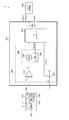
- FIG. 1 is a block diagram of the fine particle measurement system 1R using the electrical detection band method.
- the fine particle measurement system 1R includes a nanopore device 100, a measurement device 200, and a data processing device 300.
- the inside of the nanopore device 100 is filled with the electrolytic solution 2 containing the particles 4 to be detected.
- the inside of the nanopore device 100 is separated into two spaces by a nanopore chip 102, and electrodes 106 and 108 are provided in the two spaces.
- electrodes 106 and 108 are provided in the two spaces.
- the measuring device 200 generates a potential difference between the electrode pairs 106 and 108, and acquires information having a correlation with the resistance value Rp between the electrode pairs.
- the measuring device 200 includes a transimpedance amplifier 210, a voltage source 220, and a digitizer 230.
- the voltage source 220 generates a potential difference Vb between the electrode pairs 106 and 108. This potential difference Vb serves as a driving source for electrophoresis and a bias signal for measuring the resistance value Rp.
- Is Vb / Rp ... (1)
- the transimpedance amplifier 210 converts the minute current Is into a voltage signal Vs.
- Vs r ⁇ Is... (2)
- the digitizer 230 converts the voltage signal Vs into digital data Ds. In this way, the measuring device 200 can obtain a voltage signal Vs that is inversely proportional to the resistance value Rp of the pore 104.
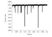
- FIG. 2 is a waveform diagram of an exemplary minute current Is measured by the measuring device 200.
- the vertical and horizontal axes of the waveform charts and time charts referred to in the present specification are appropriately enlarged or reduced for ease of understanding, and the waveforms shown are also simplified for ease of understanding. It is made, or exaggerated or emphasized.
- the resistance value Rp of the pores 104 increases for a short period of time through which the particles pass. Therefore, the current Is decreases in a pulse shape each time the particles pass through. The amount of change in the current Is has a correlation with the particle size.
- the data processing device 300 processes the digital data Ds and analyzes the number of particles 4 and the particle size distribution contained in the electrolytic solution 2.
- Japanese Unexamined Patent Publication No. 2009-014702 Japanese Unexamined Patent Publication No. 2014-209081 Japanese Unexamined Patent Publication No. 2017-12257
- the present disclosure has been made in such a situation, and one of the exemplary purposes of the embodiment is to provide a fine particle measurement system capable of accurately measuring particles.
- the fine particle measurement system applies a bias voltage corresponding to a voltage control signal to a nanopore device having pores and electrode pairs between the electrode pairs, and generates digital current data according to the current signal flowing through the nanopore device.
- the current measuring unit to be used, the voltage setting command are generated, and the current data and the voltage data including the information about the bias voltage waveform are acquired in a mode associated with each other on the time axis, based on the current data and the voltage data.
- a data processing device for determining the type of particles contained in the nanopore device is provided.
- Another aspect of the present disclosure is a measuring device.
- This measuring device is connected to a data processing device and a nanopore device having pores and electrode pairs during measurement.
- the measuring device uses a voltage source that applies a bias voltage to the electrode pair of the nanopore device, a transimpedance amplifier that detects the current flowing through the electrode pair of the nanopore device during measurement, and the output signal of the transimpedance amplifier into digital current data.
- the A / D conversion block to be converted is connected to the data processing device, the voltage source and the A / D conversion block are controlled based on the control command from the data processing device, and the bias voltage applied to the electrode pair is shown. It includes a bus controller that transmits voltage data and current data to a data processing device in a manner that can be associated with each other on the time axis.
- particles can be measured accurately.
- a nanopore device having pores and an electrode pair and a bias voltage corresponding to a voltage control signal are applied between the electrode pairs, and digital according to a current signal flowing through the nanopore device.
- the current measuring unit that generates the current data of the above, the voltage setting command is generated, and the current data and the voltage data including the information about the waveform of the bias voltage are acquired in a mode associated with each other on the time axis, and the current data is obtained.
- a data processing device for determining the type of particles contained in the nanopore device based on the voltage data.
- the voltage data may be generated at the same rate as the sampling rate of the current data.
- the voltage data may be generated each time the conditions for applying the bias voltage are changed.
- the current measuring unit may include a voltage source that generates a bias voltage according to the voltage control signal. Voltage data may be generated each time the state of the voltage source is switched.
- voltage data may be generated each time the data processor issues a voltage setting command.
- the voltage level of the bias voltage is variable, and the voltage data may include information on the voltage level of the bias voltage.
- the polarity of the bias voltage is variable, and the voltage data may include information on the polarity of the bias voltage.
- the data processing apparatus may determine the type of particles by excluding the current data obtained when the polarity of the bias voltage is reversed. Accuracy can be improved by excluding inaccurate current data.
- the measuring device is connected to a data processing device and a nanopore device having pores and electrode pairs at the time of measurement.
- the measuring device uses a voltage source that applies a bias voltage to the electrode pair of the nanopore device, a transimpedance amplifier that detects the current flowing through the electrode pair of the nanopore device during measurement, and the output signal of the transimpedance amplifier into digital current data.
- the A / D conversion block to be converted is connected to the data processing device, the voltage source and the A / D conversion block are controlled based on the control command from the data processing device, and the bias voltage applied to the electrode pair is shown. It includes a bus controller that transmits voltage data and current data to a data processing device in a manner that can be associated with each other on the time axis.
- the "state in which the member A is connected to the member B” means that the member A and the member B are physically directly connected, and that the member A and the member B are electrically connected to each other. It also includes the case of being indirectly connected via other members, which does not substantially affect the connection state, or does not impair the functions and effects performed by the combination thereof.
- a state in which the member C is provided between the member A and the member B means that the member A and the member C, or the member B and the member C are directly connected, and their electricity. It also includes the case of being indirectly connected via other members, which does not substantially affect the connection state, or does not impair the functions and effects produced by the combination thereof.
- FIG. 3 is a block diagram of the fine particle measurement system 1 according to the embodiment.
- the fine particle measurement system 1 includes a nanopore device 100, a measurement device 200, and a data processing device 300.
- the nanopore device 100 is as described with reference to FIG. 1, and includes a nanopore chip 102 provided with pores 104 and electrode pairs 106 and 108.
- the inside of the nanopore chip 102 is filled with an electrolytic solution such as KCl (potassium chloride) or PBS (phosphate buffered saline).
- the measuring device 200 is configured to be able to measure the current Is flowing through the pores 104 by applying a voltage to the electrode pairs 106 and 108.
- the measuring device 200 includes a current measuring unit 202 and a bus controller 240.
- the current measuring unit 202 applies a bias voltage Vb corresponding to the voltage control signal CTRL_V between the electrode pairs 106 and 108, and generates current data DATA_I corresponding to the current signal Is flowing through the nanopore device 100.
- the current measuring unit 202 includes a transimpedance amplifier 210, a voltage source 220, and an A / D conversion block 230.
- the voltage source 220 is a variable voltage source and generates a bias voltage Vb having a voltage level / polarity corresponding to the voltage control signal CTRL_V.
- the transimpedance amplifier 210 converts the current signal Is into a voltage signal Vs.
- the A / D conversion block 230 converts the voltage signal Vs into digital current data DATA_I.
- the bus controller 240 is configured to be able to transmit data in both directions to and from the data processing device 300.
- the bus controller 240 receives the control command CMD from the data processing device 300.
- the control command CMD includes a voltage setting command SET_V, a start command START instructing the start of measurement by the measuring device 200, and the like.
- the bus controller 240 Upon receiving the start command START, the bus controller 240 asserts the enable signal ADC_EN. Further, the voltage control signal CTRL_V corresponding to the voltage setting command SET_V is generated, and the voltage level and polarity of the bias voltage Vb generated by the voltage source 220 are controlled.
- the voltage source 220 may be a D / A converter.
- the voltage control signal CTRL_V is the digital input of the D / A converter.
- the A / D conversion block 230 includes an A / D converter 232 and an A / D conversion controller 234.
- the A / D conversion controller 234 supplies the sampling signal SMP at a predetermined sampling rate to the A / D converter 232, quantifies and captures the voltage signal Vs, and takes in the voltage signal Vs, and collects the current data DATA_I. Get as.
- the bus controller 240 transmits the current data DATA_I generated by the A / D conversion block 230 to the data processing device 300. Further, the bus controller 240 transmits the voltage data DATA_V including the information regarding the waveform of the bias voltage Vb to the data processing device 300.
- the data processing device 300 acquires the current data DATA_I and the voltage data DATA_V in a mode in which they are associated with each other on the time axis. Then, the type of the particles 4 accommodated in the nanopore device 100 is determined based on the current data DATA_I and the voltage data DATA_V.
- the data processing device 300 is an interface with the user, and also has a function of controlling the fine particle measurement system 1 in an integrated manner and acquiring, storing, and displaying the measurement result.
- the data processing device 300 may be a general-purpose computer or workstation, or may be hardware designed exclusively for the fine particle measurement system 1.
- the data processing device 300 processes the current data DATA_I and the voltage data DATA_V received from the measuring device 200, and determines the number, particle size, or type of particles 4 contained in the electrolytic solution 2. For example, the data processing device 300 may perform particle analysis processing for determining the type of particles by inputting the current data DATA_I and the voltage data DATA_V.
- the data processing device 300 is a data processing device such as a laptop computer, a desktop computer, or a tablet terminal.
- the function of the data processing device 300 described in the present specification is realized by a combination of a processor (CPU: Central Processing Unit) included in the data processing device and a software program executed by the processor.
- CPU Central Processing Unit
- FIG. 4 is a time chart showing the operation of the fine particle measurement system 1.
- the data processing device 300 executes the program and issues a command according to the program.
- Data processing device 300 issues a voltage set command SET_V the time t 0.
- the bus controller 240 varies the voltage control signal CTRL_V.
- the bias voltage Vb is set to the voltage level and polarity (+ 0.1V in this example) specified by the voltage setting command SET_V.
- the voltage signal Vs is measured by AC coupling.
- the data processing device 300 issues a start command START.
- the bus controller 240 at time t 3 asserts the enable signal adc_en, is generated a sampling signal SMP of a predetermined sampling rate, current signal Is is fetched, the current data DATA_I is generated.
- the voltage data DATA_V is preferably a bias voltage Vb actually applied to the electrode pairs 106 and 108 at each sampling time.
- the bus controller 240 receives data indicating the bias voltage Vb from the voltage source 220.
- the voltage data DATA_V may be generated based on the received data.
- the bus controller 240 may generate the voltage data DATA_V based on the voltage control signal CTRL_V generated by the bus controller 240 at each sampling time.
- Data processing apparatus 300 at time t 4 issues a voltage set command SET_V.
- the bus controller 240 varies the voltage control signal CTRL_V.
- the bias voltage Vb is changed to the voltage level and polarity (-0.1V in this example) specified by the voltage setting command SET_V. In this state, the measuring device 200 continues to measure.
- Data processing device 300 to issue the end command END to time t 6.
- the bus controller 240 in response to this, at time t 7, when negates the enable signal adc_en, uptake of the current signal Is is terminated.
- the fine particle measurement system 1 voltage application conditions can be stored together with current measurement data.
- the data processing device 300 can know the time when the voltage level and the polarity of the voltage actually change, and can be used for determining the type of particles.
- FIG. 5 is a diagram showing an example of measured current data when the polarity of the bias voltage Vb is changed.
- the data processing device 300 detects clogging of the nanopore chip 102 based on the current data DATA_I. Then, when clogging or a sign thereof is detected, the voltage setting command SET_V is generated in order to reverse the polarity of the bias voltage Vb. In other words, before and after the reversal of the polarity of the voltage occurs, there is a high possibility of clogging, and it can be said that the reliability of the current data DATA_I obtained in that state is low. Therefore, the data processing device 300 determines the type of particles by excluding the current data obtained when the polarity of the bias voltage Vb is reversed. As a result, inaccurate current data can be excluded, so that the determination accuracy can be improved.
- the voltage data DATA_V is generated at the same rate as the current data DATA_I, but not so much.
- the voltage data DATA_V may be generated every time the voltage application condition is changed. As a result, the amount of data transmitted from the measuring device 200 to the data processing device 300 can be reduced. For example, at time t 1 and time t 5 in the example of FIG. 4, may be generated voltage data DATA_V showing the application condition of the voltage.
- the voltage data DATA_V is transmitted from the bus controller 240 to the data processing device 300, but the voltage data DATA_V may be generated by the data processing device 300. If the delay time from issuing the voltage setting command SET_V to actually changing the application condition of the bias voltage Vb is short, the time when the voltage setting command SET_V is issued is regarded as the change time of the voltage application condition. And voltage data can be generated.
- the present invention relates to measurement using a nanopore device.
- Fine particle measurement system Electrolyte 4 Particles 100 Nanopore device 102 Nanopore chip 104 Pore 106, 108 Electrode 200 Measuring device 202 Current measuring unit 210 Transimpedance amplifier 220 Voltage source 230 A / D conversion block 232 A / D converter 234 A / D conversion controller 240 bus controller 300 data processing device SET_V voltage setting command CTRL_V voltage control signal DATA_I current data CMD control command START start command ADC_EN enable signal DATA_V voltage data
Landscapes
- Chemical & Material Sciences (AREA)
- Life Sciences & Earth Sciences (AREA)
- Health & Medical Sciences (AREA)
- Physics & Mathematics (AREA)
- Analytical Chemistry (AREA)
- Biochemistry (AREA)
- General Health & Medical Sciences (AREA)
- General Physics & Mathematics (AREA)
- Immunology (AREA)
- Pathology (AREA)
- Dispersion Chemistry (AREA)
- Molecular Biology (AREA)
- Chemical Kinetics & Catalysis (AREA)
- Electrochemistry (AREA)
- Investigating Or Analyzing Materials By The Use Of Electric Means (AREA)
Abstract
Description
Is=Vb/Rp …(1)
Vs=r×Is …(2)
式(1)を式(2)に代入すると、式(3)が得られる。
Vs=Vb×r/Rp …(3)
デジタイザ230は、電圧信号VsをデジタルデータDsに変換する。このように計測装置200により、細孔104の抵抗値Rpに反比例する電圧信号Vsを得ることができる。
本開示のいくつかの例示的な実施形態の概要を説明する。この概要は、後述する詳細な説明の前置きとして、実施形態の基本的な理解を目的として、1つまたは複数の実施形態のいくつかの概念を簡略化して説明するものであり、発明あるいは開示の広さを限定するものではない。またこの概要は、考えられるすべての実施形態の包括的な概要ではなく、実施形態の欠くべからざる構成要素を限定するものではない。便宜上、「一実施形態」は、本明細書に開示するひとつの実施形態または複数の実施形態を指すものとして用いる場合がある。
以下、実施形態を図面を参照しながら説明する。各図面に示される同一または同等の構成要素、部材、処理には、同一の符号を付するものとし、適宜重複した説明は省略する。また、実施形態は、開示あるいは発明を限定するものではなく例示であって、実施形態に記述されるすべての特徴やその組み合わせは、必ずしも開示あるいは発明の本質的なものであるとは限らない。
図3は、実施形態に係る微粒子測定システム1のブロック図である。微粒子測定システム1は、ナノポアデバイス100、計測装置200、データ処理装置300を備える。
実施形態では、電圧データDATA_Vが、電流データDATA_Iと同じレートで生成されたがその限りでない。電圧データDATA_Vは、電圧の印加条件が変更されるごとに生成するようにしてもよい。これにより計測装置200からデータ処理装置300に送信するデータ量を減らすことができる。たとえば図4の例では時刻t1と時刻t5において、電圧の印加条件を示す電圧データDATA_Vを生成すればよい。
バイアス電圧Vbの電圧レベルが一定であり、極性のみ反転する場合には、極性の情報のみを、電圧データDATA_Vとして保存してもよい。これにより電圧データDATA_Vのデータ量を削減できる。
実施形態では、バスコントローラ240からデータ処理装置300に、電圧データDATA_Vを送信したがその限りでなく、電圧データDATA_Vを、データ処理装置300によって生成してもよい。電圧設定コマンドSET_Vを発行してから、実際にバイアス電圧Vbの印加条件が変更されるまでの遅延時間が短い場合には、電圧設定コマンドSET_Vを発行の時刻を、電圧印加条件の変化時刻とみなして、電圧データを生成できる。
2 電解液
4 粒子
100 ナノポアデバイス
102 ナノポアチップ
104 細孔
106,108 電極
200 計測装置
202 電流測定部
210 トランスインピーダンスアンプ
220 電圧源
230 A/D変換ブロック
232 A/Dコンバータ
234 A/D変換コントローラ
240 バスコントローラ
300 データ処理装置
SET_V 電圧設定コマンド
CTRL_V 電圧制御信号
DATA_I 電流データ
CMD 制御コマンド
START スタートコマンド
ADC_EN イネーブル信号
DATA_V 電圧データ
Claims (9)
- 細孔および電極対を有するナノポアデバイスと、
電圧設定コマンドに応じたバイアス電圧を、前記電極対の間に印加するとともに、前記ナノポアデバイスに流れる電流信号に応じたデジタルの電流データを生成する電流測定部と、
前記電圧設定コマンドを生成するとともに、前記電流データと、前記バイアス電圧の波形に関する情報を含む電圧データとを、時間軸上で関連づけた態様で取得し、前記電流データと前記電圧データにもとづいて、前記ナノポアデバイスに収容される粒子の種類を判定するデータ処理装置と、
を備えることを特徴とする微粒子測定システム。 - 前記電圧データは、前記電流データのサンプリングレートと同じレートで生成されることを特徴とする請求項1に記載の微粒子測定システム。
- 前記電圧データは、前記バイアス電圧の印加条件が変更されるごとに生成されることを特徴とする請求項1に記載の微粒子測定システム。
- 前記電流測定部は、電圧制御信号に応じた前記バイアス電圧を生成する電圧源を含み、
前記電圧データは、前記電圧源の状態が切り替えられるたびに生成されることを特徴とする請求項3に記載の微粒子測定システム。 - 前記電圧データは、前記データ処理装置が前記電圧設定コマンドを発行するたびに生成されることを特徴とする請求項3に記載の微粒子測定システム。
- 前記バイアス電圧の電圧レベルは可変であり、前記電圧データは、前記バイアス電圧の電圧レベルの情報を含むことを特徴とする請求項1から5のいずれかに記載の微粒子測定システム。
- 前記バイアス電圧の極性は可変であり、前記電圧データは前記バイアス電圧の極性の情報を含むことを特徴とする請求項1から6のいずれかに記載の微粒子測定システム。
- 前記データ処理装置は、前記バイアス電圧の極性が反転したときに得られる前記電流データを除外して前記粒子の種類を判定することを特徴とする請求項7に記載の微粒子測定システム。
- 測定に際して、データ処理装置と、細孔および電極対を有するナノポアデバイスと接続される計測装置であって、
前記ナノポアデバイスの前記電極対にバイアス電圧を印加する電圧源と、
測定に際して、前記ナノポアデバイスの前記電極対に流れる電流を検出するトランスインピーダンスアンプと、
前記トランスインピーダンスアンプの出力信号をデジタルの電流データに変換するA/D変換ブロックと、
前記データ処理装置と接続され、前記データ処理装置からの制御コマンドにもとづいて、前記電圧源および前記A/D変換ブロックを制御するとともに、前記電極対に印加される前記バイアス電圧を示す電圧データと、前記電流データを、時間軸上で対応づけ可能な態様で、前記データ処理装置に送信するバスコントローラと、
を備えることを特徴とする計測装置。
Priority Applications (4)
| Application Number | Priority Date | Filing Date | Title |
|---|---|---|---|
| CN202180005845.8A CN114556083A (zh) | 2020-03-26 | 2021-01-26 | 微粒测定系统、计测装置 |
| GB2205818.4A GB2608243B (en) | 2020-03-26 | 2021-01-26 | Fine particle measuring system, and measurement device |
| DE112021000732.7T DE112021000732T5 (de) | 2020-03-26 | 2021-01-26 | Feinpartikel-messsystem und messvorrichtung |
| US17/732,833 US20220252544A1 (en) | 2020-03-26 | 2022-04-29 | Fine particle measuring system |
Applications Claiming Priority (2)
| Application Number | Priority Date | Filing Date | Title |
|---|---|---|---|
| JP2020-056582 | 2020-03-26 | ||
| JP2020056582A JP2021156712A (ja) | 2020-03-26 | 2020-03-26 | 微粒子測定システム、計測装置 |
Related Child Applications (1)
| Application Number | Title | Priority Date | Filing Date |
|---|---|---|---|
| US17/732,833 Continuation US20220252544A1 (en) | 2020-03-26 | 2022-04-29 | Fine particle measuring system |
Publications (1)
| Publication Number | Publication Date |
|---|---|
| WO2021192578A1 true WO2021192578A1 (ja) | 2021-09-30 |
Family
ID=77891227
Family Applications (1)
| Application Number | Title | Priority Date | Filing Date |
|---|---|---|---|
| PCT/JP2021/002586 Ceased WO2021192578A1 (ja) | 2020-03-26 | 2021-01-26 | 微粒子測定システム、計測装置 |
Country Status (6)
| Country | Link |
|---|---|
| US (1) | US20220252544A1 (ja) |
| JP (1) | JP2021156712A (ja) |
| CN (1) | CN114556083A (ja) |
| DE (1) | DE112021000732T5 (ja) |
| GB (1) | GB2608243B (ja) |
| WO (1) | WO2021192578A1 (ja) |
Families Citing this family (3)
| Publication number | Priority date | Publication date | Assignee | Title |
|---|---|---|---|---|
| JP2024176883A (ja) * | 2023-06-09 | 2024-12-19 | 株式会社アドバンテスト | 微粒子測定装置および微粒子測定方法 |
| JP2024176884A (ja) * | 2023-06-09 | 2024-12-19 | 株式会社アドバンテスト | 微粒子測定装置 |
| CN120866793B (zh) * | 2025-09-28 | 2026-02-24 | 中国科学院上海技术物理研究所 | 一种硒碲化钒材料的制备方法、制备系统、产品和应用 |
Citations (8)
| Publication number | Priority date | Publication date | Assignee | Title |
|---|---|---|---|---|
| JPS61153545A (ja) * | 1984-12-27 | 1986-07-12 | Toshiba Corp | 粒子分析装置 |
| JP2004233356A (ja) * | 2003-01-27 | 2004-08-19 | Agilent Technol Inc | ナノポアを通って移動するバイオポリマーの識別装置及び方法 |
| JP2010524436A (ja) * | 2007-04-04 | 2010-07-22 | ザ リージェンツ オブ ザ ユニバーシティ オブ カリフォルニア | ナノポアを使用するための組成物、デバイス、システム、及び方法 |
| JP2011501806A (ja) * | 2007-10-02 | 2011-01-13 | プレジデント アンド フェロウズ オブ ハーバード カレッジ | ナノポアによる分子の捕捉、再捕捉およびトラッピング |
| WO2015121394A1 (en) * | 2014-02-14 | 2015-08-20 | Ecole Polytechnique Federale De Lausanne (Epfl) | Molecular sensing device |
| JP2017120257A (ja) * | 2015-12-25 | 2017-07-06 | 国立大学法人大阪大学 | 分類分析方法、分類分析装置および分類分析用記憶媒体 |
| US20180164205A1 (en) * | 2015-06-12 | 2018-06-14 | Imperial Innovations Lilmited | Apparatus and method |
| WO2020044780A1 (ja) * | 2018-08-28 | 2020-03-05 | 株式会社日立ハイテクノロジーズ | 生体分子分析装置 |
Family Cites Families (9)
| Publication number | Priority date | Publication date | Assignee | Title |
|---|---|---|---|---|
| CN102725060B (zh) * | 2009-12-02 | 2015-09-02 | 国立研究开发法人科学技术振兴机构 | 流路装置以及包含流路装置的样品处理装置 |
| US8828138B2 (en) * | 2010-05-17 | 2014-09-09 | International Business Machines Corporation | FET nanopore sensor |
| CN102539503A (zh) * | 2010-12-30 | 2012-07-04 | 中国科学院沈阳自动化研究所 | 一种纳流控芯片及基于afm的加工方法和应用 |
| US9551697B2 (en) * | 2013-10-17 | 2017-01-24 | Genia Technologies, Inc. | Non-faradaic, capacitively coupled measurement in a nanopore cell array |
| US9921181B2 (en) * | 2014-06-26 | 2018-03-20 | International Business Machines Corporation | Detection of translocation events using graphene-based nanopore assemblies |
| JP6653767B2 (ja) * | 2016-12-09 | 2020-02-26 | 株式会社日立ハイテクノロジーズ | ナノポア形成方法、ナノポア形成装置及び生体分子計測装置 |
| JP7111545B2 (ja) * | 2018-07-26 | 2022-08-02 | 株式会社アドバンテスト | 計測装置および微粒子測定システム |
| JP7082013B2 (ja) * | 2018-09-04 | 2022-06-07 | 株式会社アドバンテスト | 微粒子測定システム、計測装置 |
| CN110488013B (zh) * | 2019-07-26 | 2023-02-28 | 东南大学 | 结合纳米孔技术的肿瘤标志miRNA检测装置及方法 |
-
2020
- 2020-03-26 JP JP2020056582A patent/JP2021156712A/ja active Pending
-
2021
- 2021-01-26 WO PCT/JP2021/002586 patent/WO2021192578A1/ja not_active Ceased
- 2021-01-26 CN CN202180005845.8A patent/CN114556083A/zh active Pending
- 2021-01-26 DE DE112021000732.7T patent/DE112021000732T5/de active Pending
- 2021-01-26 GB GB2205818.4A patent/GB2608243B/en active Active
-
2022
- 2022-04-29 US US17/732,833 patent/US20220252544A1/en not_active Abandoned
Patent Citations (8)
| Publication number | Priority date | Publication date | Assignee | Title |
|---|---|---|---|---|
| JPS61153545A (ja) * | 1984-12-27 | 1986-07-12 | Toshiba Corp | 粒子分析装置 |
| JP2004233356A (ja) * | 2003-01-27 | 2004-08-19 | Agilent Technol Inc | ナノポアを通って移動するバイオポリマーの識別装置及び方法 |
| JP2010524436A (ja) * | 2007-04-04 | 2010-07-22 | ザ リージェンツ オブ ザ ユニバーシティ オブ カリフォルニア | ナノポアを使用するための組成物、デバイス、システム、及び方法 |
| JP2011501806A (ja) * | 2007-10-02 | 2011-01-13 | プレジデント アンド フェロウズ オブ ハーバード カレッジ | ナノポアによる分子の捕捉、再捕捉およびトラッピング |
| WO2015121394A1 (en) * | 2014-02-14 | 2015-08-20 | Ecole Polytechnique Federale De Lausanne (Epfl) | Molecular sensing device |
| US20180164205A1 (en) * | 2015-06-12 | 2018-06-14 | Imperial Innovations Lilmited | Apparatus and method |
| JP2017120257A (ja) * | 2015-12-25 | 2017-07-06 | 国立大学法人大阪大学 | 分類分析方法、分類分析装置および分類分析用記憶媒体 |
| WO2020044780A1 (ja) * | 2018-08-28 | 2020-03-05 | 株式会社日立ハイテクノロジーズ | 生体分子分析装置 |
Also Published As
| Publication number | Publication date |
|---|---|
| GB2608243B (en) | 2024-12-25 |
| JP2021156712A (ja) | 2021-10-07 |
| GB2608243A (en) | 2022-12-28 |
| CN114556083A (zh) | 2022-05-27 |
| GB202205818D0 (en) | 2022-06-08 |
| US20220252544A1 (en) | 2022-08-11 |
| DE112021000732T5 (de) | 2022-12-01 |
Similar Documents
| Publication | Publication Date | Title |
|---|---|---|
| JP2021156712A (ja) | 微粒子測定システム、計測装置 | |
| JP7082013B2 (ja) | 微粒子測定システム、計測装置 | |
| US10690625B2 (en) | Measuring electrophoretic mobility | |
| JP6416600B2 (ja) | 測定装置 | |
| CN115950938B (zh) | 一种电化学生物传感器的制作方法及电化学检测仪 | |
| WO2020066472A1 (ja) | 電解質測定装置 | |
| JP7082015B2 (ja) | 計測装置 | |
| US11320398B2 (en) | Sensor arrangement for voltammetry | |
| JP2014235168A (ja) | 時分割多重位相検波方式の手持ち式試験測定器 | |
| GB2590883A (en) | Measuring electrophoretic mobility | |
| EP4306948A1 (en) | Validation of electrochemical measurements using a potentiostat | |
| RU2093134C1 (ru) | Способ определения кинетических параметров электрических потенциалов точек акупунктуры при диагностике организма и устройство для его осуществления | |
| CN221690948U (zh) | 一种电化学浓度检测电路和血糖浓度检测设备 | |
| JP7839287B2 (ja) | 溶液中の粒子の測定方法およびそれを実施するための装置 | |
| JP3186012U (ja) | 電気化学分析装置 | |
| JP5609722B2 (ja) | 通電回路およびインピーダンス測定回路 | |
| EP4621399A1 (en) | Measurement apparatus and measurement method | |
| WO2024252999A1 (ja) | 微粒子測定装置および微粒子測定方法 | |
| JP7215303B2 (ja) | 測定装置 | |
| TWI687207B (zh) | 檢測裝置及檢測方法 | |
| Reagen et al. | Dual-Channel Potentiostat for Electrochemical Measurements with Approximations | |
| JPS62207968A (ja) | 導電率計回路 | |
| KR20240174452A (ko) | Pwm을 활용한 임피던스 모니터링 장치 및 방법 | |
| RU2549550C1 (ru) | Кулонометрическая потенциостатическая установка | |
| JP2004294162A (ja) | 電磁流量計 |
Legal Events
| Date | Code | Title | Description |
|---|---|---|---|
| 121 | Ep: the epo has been informed by wipo that ep was designated in this application |
Ref document number: 21776301 Country of ref document: EP Kind code of ref document: A1 |
|
| WWE | Wipo information: entry into national phase |
Ref document number: 2205818.4 Country of ref document: GB |
|
| WWP | Wipo information: published in national office |
Ref document number: 2205818.4 Country of ref document: GB |
|
| 122 | Ep: pct application non-entry in european phase |
Ref document number: 21776301 Country of ref document: EP Kind code of ref document: A1 |
|
| WWG | Wipo information: grant in national office |
Ref document number: 2205818.4 Country of ref document: GB |