WO2021187282A1 - 面発光レーザ - Google Patents
面発光レーザ Download PDFInfo
- Publication number
- WO2021187282A1 WO2021187282A1 PCT/JP2021/009661 JP2021009661W WO2021187282A1 WO 2021187282 A1 WO2021187282 A1 WO 2021187282A1 JP 2021009661 W JP2021009661 W JP 2021009661W WO 2021187282 A1 WO2021187282 A1 WO 2021187282A1
- Authority
- WO
- WIPO (PCT)
- Prior art keywords
- layer
- dbr
- type
- emitting laser
- doped
- Prior art date
- Legal status (The legal status is an assumption and is not a legal conclusion. Google has not performed a legal analysis and makes no representation as to the accuracy of the status listed.)
- Ceased
Links
Images




Classifications
-
- H—ELECTRICITY
- H01—ELECTRIC ELEMENTS
- H01S—DEVICES USING THE PROCESS OF LIGHT AMPLIFICATION BY STIMULATED EMISSION OF RADIATION [LASER] TO AMPLIFY OR GENERATE LIGHT; DEVICES USING STIMULATED EMISSION OF ELECTROMAGNETIC RADIATION IN WAVE RANGES OTHER THAN OPTICAL
- H01S5/00—Semiconductor lasers
- H01S5/04—Processes or apparatus for excitation, e.g. pumping, e.g. by electron beams
- H01S5/042—Electrical excitation ; Circuits therefor
- H01S5/0425—Electrodes, e.g. characterised by the structure
- H01S5/04256—Electrodes, e.g. characterised by the structure characterised by the configuration
- H01S5/04257—Electrodes, e.g. characterised by the structure characterised by the configuration having positive and negative electrodes on the same side of the substrate
-
- H—ELECTRICITY
- H01—ELECTRIC ELEMENTS
- H01S—DEVICES USING THE PROCESS OF LIGHT AMPLIFICATION BY STIMULATED EMISSION OF RADIATION [LASER] TO AMPLIFY OR GENERATE LIGHT; DEVICES USING STIMULATED EMISSION OF ELECTROMAGNETIC RADIATION IN WAVE RANGES OTHER THAN OPTICAL
- H01S5/00—Semiconductor lasers
- H01S5/10—Construction or shape of the optical resonator, e.g. extended or external cavity, coupled cavities, bent-guide, varying width, thickness or composition of the active region
- H01S5/18—Surface-emitting [SE] lasers, e.g. having both horizontal and vertical cavities
- H01S5/183—Surface-emitting [SE] lasers, e.g. having both horizontal and vertical cavities having only vertical cavities, e.g. vertical cavity surface-emitting lasers [VCSEL]
- H01S5/18341—Intra-cavity contacts
-
- H—ELECTRICITY
- H01—ELECTRIC ELEMENTS
- H01S—DEVICES USING THE PROCESS OF LIGHT AMPLIFICATION BY STIMULATED EMISSION OF RADIATION [LASER] TO AMPLIFY OR GENERATE LIGHT; DEVICES USING STIMULATED EMISSION OF ELECTROMAGNETIC RADIATION IN WAVE RANGES OTHER THAN OPTICAL
- H01S5/00—Semiconductor lasers
- H01S5/04—Processes or apparatus for excitation, e.g. pumping, e.g. by electron beams
- H01S5/042—Electrical excitation ; Circuits therefor
- H01S5/0421—Electrical excitation ; Circuits therefor characterised by the semiconducting contacting layers
-
- H—ELECTRICITY
- H01—ELECTRIC ELEMENTS
- H01S—DEVICES USING THE PROCESS OF LIGHT AMPLIFICATION BY STIMULATED EMISSION OF RADIATION [LASER] TO AMPLIFY OR GENERATE LIGHT; DEVICES USING STIMULATED EMISSION OF ELECTROMAGNETIC RADIATION IN WAVE RANGES OTHER THAN OPTICAL
- H01S5/00—Semiconductor lasers
- H01S5/04—Processes or apparatus for excitation, e.g. pumping, e.g. by electron beams
- H01S5/042—Electrical excitation ; Circuits therefor
- H01S5/0425—Electrodes, e.g. characterised by the structure
- H01S5/04256—Electrodes, e.g. characterised by the structure characterised by the configuration
-
- H—ELECTRICITY
- H01—ELECTRIC ELEMENTS
- H01S—DEVICES USING THE PROCESS OF LIGHT AMPLIFICATION BY STIMULATED EMISSION OF RADIATION [LASER] TO AMPLIFY OR GENERATE LIGHT; DEVICES USING STIMULATED EMISSION OF ELECTROMAGNETIC RADIATION IN WAVE RANGES OTHER THAN OPTICAL
- H01S5/00—Semiconductor lasers
- H01S5/10—Construction or shape of the optical resonator, e.g. extended or external cavity, coupled cavities, bent-guide, varying width, thickness or composition of the active region
- H01S5/18—Surface-emitting [SE] lasers, e.g. having both horizontal and vertical cavities
- H01S5/183—Surface-emitting [SE] lasers, e.g. having both horizontal and vertical cavities having only vertical cavities, e.g. vertical cavity surface-emitting lasers [VCSEL]
- H01S5/18308—Surface-emitting [SE] lasers, e.g. having both horizontal and vertical cavities having only vertical cavities, e.g. vertical cavity surface-emitting lasers [VCSEL] having a special structure for lateral current or light confinement
- H01S5/18311—Surface-emitting [SE] lasers, e.g. having both horizontal and vertical cavities having only vertical cavities, e.g. vertical cavity surface-emitting lasers [VCSEL] having a special structure for lateral current or light confinement using selective oxidation
-
- H—ELECTRICITY
- H01—ELECTRIC ELEMENTS
- H01S—DEVICES USING THE PROCESS OF LIGHT AMPLIFICATION BY STIMULATED EMISSION OF RADIATION [LASER] TO AMPLIFY OR GENERATE LIGHT; DEVICES USING STIMULATED EMISSION OF ELECTROMAGNETIC RADIATION IN WAVE RANGES OTHER THAN OPTICAL
- H01S5/00—Semiconductor lasers
- H01S5/10—Construction or shape of the optical resonator, e.g. extended or external cavity, coupled cavities, bent-guide, varying width, thickness or composition of the active region
- H01S5/18—Surface-emitting [SE] lasers, e.g. having both horizontal and vertical cavities
- H01S5/183—Surface-emitting [SE] lasers, e.g. having both horizontal and vertical cavities having only vertical cavities, e.g. vertical cavity surface-emitting lasers [VCSEL]
- H01S5/18344—Surface-emitting [SE] lasers, e.g. having both horizontal and vertical cavities having only vertical cavities, e.g. vertical cavity surface-emitting lasers [VCSEL] characterized by the mesa, e.g. dimensions or shape of the mesa
- H01S5/18347—Mesa comprising active layer
-
- H—ELECTRICITY
- H01—ELECTRIC ELEMENTS
- H01S—DEVICES USING THE PROCESS OF LIGHT AMPLIFICATION BY STIMULATED EMISSION OF RADIATION [LASER] TO AMPLIFY OR GENERATE LIGHT; DEVICES USING STIMULATED EMISSION OF ELECTROMAGNETIC RADIATION IN WAVE RANGES OTHER THAN OPTICAL
- H01S5/00—Semiconductor lasers
- H01S5/10—Construction or shape of the optical resonator, e.g. extended or external cavity, coupled cavities, bent-guide, varying width, thickness or composition of the active region
- H01S5/18—Surface-emitting [SE] lasers, e.g. having both horizontal and vertical cavities
- H01S5/183—Surface-emitting [SE] lasers, e.g. having both horizontal and vertical cavities having only vertical cavities, e.g. vertical cavity surface-emitting lasers [VCSEL]
- H01S5/18361—Structure of the reflectors, e.g. hybrid mirrors
- H01S5/18377—Structure of the reflectors, e.g. hybrid mirrors comprising layers of different kind of materials, e.g. combinations of semiconducting with dielectric or metallic layers
-
- H—ELECTRICITY
- H01—ELECTRIC ELEMENTS
- H01S—DEVICES USING THE PROCESS OF LIGHT AMPLIFICATION BY STIMULATED EMISSION OF RADIATION [LASER] TO AMPLIFY OR GENERATE LIGHT; DEVICES USING STIMULATED EMISSION OF ELECTROMAGNETIC RADIATION IN WAVE RANGES OTHER THAN OPTICAL
- H01S2301/00—Functional characteristics
- H01S2301/17—Semiconductor lasers comprising special layers
- H01S2301/176—Specific passivation layers on surfaces other than the emission facet
-
- H—ELECTRICITY
- H01—ELECTRIC ELEMENTS
- H01S—DEVICES USING THE PROCESS OF LIGHT AMPLIFICATION BY STIMULATED EMISSION OF RADIATION [LASER] TO AMPLIFY OR GENERATE LIGHT; DEVICES USING STIMULATED EMISSION OF ELECTROMAGNETIC RADIATION IN WAVE RANGES OTHER THAN OPTICAL
- H01S5/00—Semiconductor lasers
- H01S5/10—Construction or shape of the optical resonator, e.g. extended or external cavity, coupled cavities, bent-guide, varying width, thickness or composition of the active region
- H01S5/18—Surface-emitting [SE] lasers, e.g. having both horizontal and vertical cavities
- H01S5/183—Surface-emitting [SE] lasers, e.g. having both horizontal and vertical cavities having only vertical cavities, e.g. vertical cavity surface-emitting lasers [VCSEL]
- H01S5/18358—Surface-emitting [SE] lasers, e.g. having both horizontal and vertical cavities having only vertical cavities, e.g. vertical cavity surface-emitting lasers [VCSEL] containing spacer layers to adjust the phase of the light wave in the cavity
Definitions
- This disclosure relates to a surface emitting laser.
- the surface emitting laser is disclosed in, for example, Patent Documents 1 and 2.
- Surface emitting lasers are required to have both high light output and low drive voltage. Therefore, it is desirable to provide a surface emitting laser capable of achieving both a high light output and a low drive voltage.
- the surface emitting laser includes a first DBR (distributed Bragg reflector) layer, an active layer, a second DBR layer and a first conductive contact layer in this order, and further comprises a first DBR layer and an active layer. It has a laminated structure including a second conductive contact layer and a two-dimensional electron gas generation layer in between or in the first DBR layer.
- the surface emitting laser further includes a first electrode layer in contact with the first conductive type contact layer and a second electrode layer in contact with the second conductive type contact layer.
- the driving voltage of the surface emitting laser is reduced by the second conductive type contact layer in contact with the second electrode layer, and the surface emitting laser is provided near the second conductive type contact layer 2
- the dimensional electron gas generation layer ensures carrier transport even when the second conductive contact layer is thinned.
- FIG. 1 shows an example of cross-sectional configuration of the surface emitting laser 1.
- the surface emitting laser 1 is provided with a vertical resonator on the substrate 10.
- the vertical resonator is configured to oscillate at an oscillation wavelength of ⁇ 0 by two DBR (distributed Bragg reflector) layers (n-type DBR layer 21 and p-type DBR layer 27) facing each other in the normal direction of the substrate 10. .
- the n-type DBR layer 21 corresponds to a specific example of the “first DBR layer” of the present disclosure.
- the p-type DBR layer 27 corresponds to a specific example of the “second DBR layer” of the present disclosure.
- the n-type DBR layer 21 is formed at a position closer to the substrate 10 than the p-type DBR layer 27.
- the p-type DBR layer 27 is formed at a position distant from the substrate 10 as compared with the n-type DBR layer 21.
- the surface emitting laser 1 is configured so that the laser beam L is emitted from the p-type DBR layer 27 side. Therefore, the surface emitting laser 1 is a top emitting type laser having a light emitting surface 1S of the laser beam L on the upper surface.
- the surface emitting laser 1 includes an epitaxial laminated structure 20 formed on a substrate 10 by an epitaxial crystal growth method using the substrate 10 as a crystal growth substrate.
- the epitaxial laminated structure 20 includes, for example, an n-type DBR layer 21, a two-dimensional electron gas generation layer 22, an n-type contact layer 23, a spacer layer 24, an active layer 25, a spacer layer 26, a p-type DBR layer 27, and a p-type contact layer. 28 is included in this order from the substrate 10 side.
- the n-type contact layer 23 corresponds to a specific example of the "first conductive type contact layer" of the present disclosure.
- the p-type contact layer 28 corresponds to a specific example of the “second conductive type contact layer” of the present disclosure.
- the spacer layer 24, the active layer 25, the spacer layer 26, the p-type DBR layer 27, and the p-type contact layer 28 constitute a columnar mesa portion 20A extending in the normal direction of the substrate 10. doing.
- the two-dimensional electron gas generation layer 22 and the n-type contact layer 23 are provided in the region on the n-type DBR layer 21 side in the positional relationship with the mesa portion 20A.
- the two-dimensional electron gas generation layer 22 is provided at least at a position facing the mesa portion 20A and the electrode layer 31 with the n-type contact layer 23 in between.
- the n-type contact layer 23 is formed at a position closer to the active layer 25 than the two-dimensional electron gas generation layer 22.
- the two-dimensional electron gas generation layer 22 and the n-type contact layer 23 are provided between the n-type DBR layer 21 and the active layer 25.
- the substrate 10 is arranged at a position facing the mesa portion 20A via the two-dimensional electron gas generation layer 22 and the n-type contact layer 23.
- the surface emitting laser 1 includes an electrode layer 32 in contact with the top of the mesa portion 20A (that is, the p-type contact layer 28), and includes an electrode layer 31 in contact with the n-type contact layer 23 extending to the skirt of the mesa portion 20A.
- the p-type contact layer 28 is a layer for ohmic contacting the p-type DBR layer 27 and the electrode layer 32 with each other.
- the n-type contact layer 23 is a layer that serves as a current path between the electrode layer 31 and the central portion of the mesa portion 20A.
- the electrode layer 32 has, for example, a ring shape having an opening at least at a position facing the light emitting region of the active layer 25.
- the surface exposed in the opening of the electrode layer 32 is the light emitting surface 1S.
- the electrode layer 31 is in contact with the surface of the n-type contact layer 23 on the active layer 25 side, which corresponds to the skirt of the mesa portion 20A (that is, the exposed surface that is not covered by the mesa portion 20A and is exposed). ing.
- the electrode layer 32 corresponds to a specific example of the “first electrode layer” of the present disclosure.
- the electrode layer 31 corresponds to a specific example of the “second electrode layer” of the present disclosure.
- the surface emitting laser 1 is formed of, for example, an arsenic semiconductor.
- the arsenic semiconductor refers to a compound semiconductor containing an arsenic (As) element and at least one of aluminum (Al), gallium (Ga), and indium (In).
- the substrate 10 is, for example, an n-type semiconductor substrate. Examples of the n-type semiconductor substrate that can be used for the substrate 10 include an n-type GaAs substrate.
- the substrate 10 may be a semi-insulating semiconductor substrate. Examples of the semi-insulating semiconductor substrate that can be used for the substrate 10 include a GaAs substrate.
- the substrate 10 may be a semi-insulating semiconductor substrate from the viewpoint of reducing the absorption of light emitted from the active layer 25. Examples of the semi-insulating semiconductor substrate that can be used for the substrate 10 include a semi-insulating GaAs substrate.
- the n-type DBR layer 21 is formed by alternately laminating low refractive index layers (not shown) and high refractive index layers (not shown).
- the low refractive index layer is composed of, for example, n-type Alx1Ga1-x1As (0 ⁇ x1 ⁇ 1) having an optical thickness of ⁇ 0 ⁇ 1/4 ( ⁇ 0 is an oscillation wavelength), and the high refractive index layer is, for example. It is composed of n-type Alx2Ga1-x2As (0 ⁇ x2 ⁇ x1) having an optical thickness of ⁇ 0 ⁇ 1/4.
- the two-dimensional electron gas generation layer 22 is configured to be capable of generating a state in which electrons are two-dimensionally distributed in the semiconductor layer.
- the two-dimensional electron gas generation layer 22 is configured such that, for example, a barrier is created in the conduction band at the boundary between two types of laminated semiconductor layers, and the Fermi level is above the conduction band by adjusting the voltage and doping. ing.
- the two-dimensional electron gas generation layer 22 is formed in a laminated body composed of, for example, a non-doped GaAs layer 22c, a non-doped AlGaAs layer 22b, and an n-type AlGaAs layer 22a in this order from the n-type contact layer 23 side.
- the two-dimensional electron gas generation layer 22 is formed in, for example, an n-type AlGaAs layer 22a, a non-doped AlGaAs layer 22b, and a non-doped GaAs layer 22c laminated in this order on an n-type DBR layer 21. ..
- a barrier is formed in the conduction band near the boundary between the non-doped GaAs layer 22c and the non-doped AlGaAs layer 22b, and the Fermi level EF is formed. It is above the conduction band. Therefore, of the non-doped GaAs layer 22c, the two-dimensional electron gas generation layer 22 is formed near the boundary between the non-doped GaAs layer 22c and the non-doped AlGaAs layer 22b.
- the n-type contact layer 23 is made of, for example, n-type GaAs.
- the spacer layer 24 is made of, for example, n-type Alx3Ga1-x3As (0 ⁇ x3 ⁇ 1). Examples of the n-type impurities in the n-type DBR layer 21, the n-type AlGaAs layer 22a, the n-type contact layer 23, and the spacer layer 24 include silicon (Si).
- the active layer 25 is, for example, a barrier layer (not shown) composed of an undoped Inx4Ga1-x4As (0 ⁇ x4 ⁇ 1) well layer (not shown) and an undoped Alx5Ga1-x5As (0 ⁇ x5 ⁇ 1). It has a multiple quantum well structure in which The region of the active layer 25 facing the current injection region 29B (described later) is the light emitting region.
- the spacer layer 26 is made of, for example, p-type Alx6Ga1-x6As (0 ⁇ x6 ⁇ 1).
- the p-type DBR layer 27 is formed by alternately laminating low refractive index layers (not shown) and high refractive index layers (not shown).
- the low refractive index layer is composed of, for example, p-type Alx7Ga1-x7As (0 ⁇ x7 ⁇ 1) having an optical thickness of ⁇ 0 ⁇ 1/4
- the high refractive index layer is, for example, an optical thickness of ⁇ 0 ⁇ . It is composed of 1/4 n-type Alx8Ga1-x8As (0 ⁇ x8 ⁇ x7).
- the p-type DBR layer 27 is configured to have a smaller reflectance with respect to the oscillation wavelength ⁇ 0 of the vertical resonator in the mesa portion 20A as compared with the n-type DBR layer 21.
- the p-type DBR layer 27 is formed thinner than, for example, the n-type DBR layer 21.
- the p-type contact layer 28 is made of, for example, p-type Alx9Ga1-x9As (0 ⁇ x9 ⁇ 1). Examples of the p-type impurities in the spacer layer 26, the p-type DBR layer 27 and the p-type contact layer 28 include carbon (C).
- the epitaxial laminated structure 20 has a current constriction layer 29 in the p-type DBR layer 27 or between the p-type DBR layer 27 and the spacer layer 26.
- the current constriction layer 29 has a current injection region 29B and a current constriction region 29A.
- the current constriction region 29A is formed in a peripheral region of the current injection region 29B.
- the current injection region 29B is composed of, for example, p-type Alx10Ga1-x10As (0 ⁇ x10 ⁇ 1).
- the current constriction region 29A is composed of, for example, Al2O3 (aluminum oxide), and can be obtained, for example, by oxidizing a high concentration of Al contained in the AlAs layer described later from the side surface. Therefore, the current constriction layer 29 has a function of constricting the current.
- the electrode layer 31 is in contact with the surface of the n-type contact layer 23 on the mesa portion 20A side.
- the electrode layer 31 is composed of an alloy, and is, for example, a laminated body formed by laminating AuGe, Ni, and Au in order from the n-type contact layer 23 side.
- the electrode layer 32 is made of a non-alloy, and is, for example, a laminated body formed by laminating Ti, Pt, and Au in order from the p-type contact layer 28 side.
- An insulating layer 33 is formed around the mesa portion 20A.
- the insulating layer 33 is a layer for protecting the mesa portion 20A, and is composed of, for example, SiO2 or Si3N4.
- compound semiconductors are collectively formed on a substrate 10 made of GaAs, for example, by an epitaxial crystal growth method such as a MOCVD (Metal Organic Chemical Vapor Deposition) method. do.
- MOCVD Metal Organic Chemical Vapor Deposition
- raw materials for the compound semiconductor for example, methylaluminum (TMAl), trimethylgallium (TMGa), trimethylindium (TMIn) and other methyl-based organometallic gases and arsine (AsH3) gas are used as raw materials for donor impurities.
- As the raw material of the acceptor impurity for example, disilane (Si2H6) is used, and for example, carbon tetrabromide (CBr4) is used.
- an n-type DBR layer 21, a two-dimensional electron gas generation layer 22, an n-type contact layer 23, a spacer layer 24, an active layer 25, and a spacer layer are applied by an epitaxial crystal growth method such as the MOCVD method.
- an epitaxial laminated structure 20 including a p-type DBR layer 27 and a p-type contact layer 28 is formed.
- the epitaxial laminated structure 20 is selectively etched using this resist layer as a mask, and the epitaxial laminated structure 20 is epitaxially laminated to a depth reaching the n-type contact layer 23.
- the structure 20 is etched.
- RIE Reactive Ion Etching
- Cl-based gas Cl-based gas.
- the columnar mesa portion 20A is formed.
- the n-type contact layer 23 is exposed at the skirt of the mesa portion 20A.
- an AlAs layer is formed at a position where the current constriction layer 29 is formed, and the AlAs layer is exposed on the side surface of the mesa portion 20A.
- the resist layer is removed.
- an oxidation treatment is performed at a high temperature to selectively oxidize Al contained in the AlAs layer from the side surface of the mesa portion 20A.
- Al contained in the AlAs layer is selectively oxidized from the side surface of the mesa portion 20A by a wet oxidation method.
- the outer edge region of the AlAs layer becomes an insulating layer (aluminum oxide), and the current constriction layer 29 is formed.
- the insulating layer 33 covering the mesa portion 20A is formed.
- an opening is formed at a predetermined position in the skirt of the mesa portion 20A.
- an electrode layer 31 in contact with the surface (exposed surface) on the mesa portion 20A side of the n-type contact layer 23 is formed in the opening. In this way, the surface emitting laser 1 is manufactured.
- the electrode layer 31 is provided on the back surface of the substrate 10.
- the substrate 10 is composed of, for example, an n-type GaAs substrate, and a laser is applied by applying a predetermined voltage between the electrode layer 32 on the mesa portion 20A and the electrode layer 31 provided on the back surface of the substrate 10. Oscillation occurs. At this time, the drive voltage increases due to the resistance component in the thickness direction of the substrate 10 and the n-type DBR layer 21.
- the n-type contact layer 23 is thickly formed. As a result, the resistance component in the lateral direction is lowered, and the driving voltage is reduced. However, since the n-type contact layer 23 is formed thick, light absorption occurs in the n-type contact layer 23, the threshold current deteriorates, and the light output decreases.
- the driving voltage of the surface emitting laser 1 is reduced by the n-type contact layer 23 in contact with the electrode layer 31, and the two-dimensional electron gas generation layer 22 provided near the n-type contact layer 23 reduces the drive voltage. Even when the n-type contact layer 23 is thinned, carrier transportation is ensured. When the n-type contact layer 23 is formed thin, the light absorption in the n-type contact layer 23 is suppressed, the threshold current is reduced, and the light output is improved. On the other hand, the presence of the two-dimensional electron gas generation layer 22 ensures the transport of carriers in the lateral direction, so that the resistance component in the lateral direction is lowered and the driving voltage is reduced. Therefore, in the present embodiment, both high optical output and low drive voltage can be achieved at the same time.
- the n-type contact layer 23 is formed at a position closer to the active layer 25 than the two-dimensional electron gas generation layer 22, and the electrode layer 31 is the surface of the n-type contact layer 23 on the active layer 25 side. It touches the exposed surface).
- the mesa portion 20A can be formed and at the same time, the exposed surface of the n-type contact layer 23 can be formed. Therefore, both high optical output and low drive voltage can be achieved without providing a special process in the manufacturing process.
- the two-dimensional electron gas generation layer 22 includes the non-doped GaAs layer 22c, the non-doped AlGaAs layer 22b, and the n-type AlGaAs layer 22a in this order from the n-type contact layer 23 side, and is composed of the non-doped GaAs layer.
- the two-dimensional electron gas generation layer 22 is formed near the boundary between the non-doped GaAs layer 22c and the non-doped AlGaAs layer 22b. Since the two-dimensional electron gas generation layer 22 can be formed by using the non-doped layer in this way, the light absorption in the two-dimensional electron gas generation layer 22 is suppressed, the threshold current is reduced, and the light output is improved. do. Therefore, both high optical output and low drive voltage can be achieved at the same time.
- the spacer layer 24, the active layer 25, the spacer layer 26, the p-type DBR layer 27, and the p-type contact layer 28 constitute a columnar mesa portion 20A extending in the normal direction of the substrate 10. doing.
- the two-dimensional electron gas generation layer 22, the spacer layer 24, the active layer 25, the spacer layer 26, the p-type DBR layer 27, and the p-type contact layer 28 are the substrates 10 in the epitaxial laminated structure 20.
- An example is illustrated in which a columnar mesa portion 20A extending in the normal direction of the above is formed.
- the two-dimensional electron gas generation layer 22 is formed in a laminated body composed of, for example, a non-doped GaAs layer 22c, a non-doped AlGaAs layer 22b, and an n-type AlGaAs layer 22a in this order from the n-type contact layer 23 side.
- the two-dimensional electron gas generation layer 22 is formed in, for example, a laminated body formed by laminating a non-doped GaAs layer 22c, a non-doped AlGaAs layer 22b, and an n-type AlGaAs layer 22a on an n-type contact layer 23 in this order. ..
- the non-doped GaAs layer 22c in the non-doped GaAs layer 22c, a barrier is formed in the conduction band near the boundary between the non-doped GaAs layer 22c and the non-doped AlGaAs layer 22b.
- the Fermi level EF is above the conduction band. Therefore, of the non-doped GaAs layer 22c, the two-dimensional electron gas generation layer 22 is formed near the boundary between the non-doped GaAs layer 22c and the non-doped AlGaAs layer 22b.
- the drive voltage of the surface emitting laser 1 is reduced by the n-type contact layer 23 in contact with the electrode layer 31, and the two-dimensional electron gas provided near the n-type contact layer 23 is provided.
- the generation layer 22 ensures carrier transport even when the n-type contact layer 23 is thinned.
- the n-type contact layer 23 is formed thin, the light absorption in the n-type contact layer 23 is suppressed, the threshold current is reduced, and the light output is improved.
- the presence of the two-dimensional electron gas generation layer 22 ensures the transport of carriers in the lateral direction, so that the resistance component in the lateral direction is lowered and the driving voltage is reduced. Therefore, even in this modified example, both high optical output and low drive voltage can be achieved at the same time.
- the two-dimensional electron gas generation layer 22 is formed at a position closer to the active layer 25 than the n-type contact layer 23, and the electrode layer 31 corresponds to the skirt of the mesa portion 20A of the n-type contact layer 23. It is in contact with a portion (that is, an exposed surface 2S that is exposed without being covered with the two-dimensional electron gas generation layer 22).
- a portion that is, an exposed surface 2S that is exposed without being covered with the two-dimensional electron gas generation layer 22.
- the surface emitting laser 1 is a top emitting type that emits the laser light L from the upper surface of the mesa portion 20A, but is a back emitting type that emits the laser light L from the substrate 10 side. It may be.
- the substrate 10 may be omitted.
- the substrate 10 can be peeled off by, for example, providing a lift-off layer between the substrate 10 and the epitaxial laminated structure 20 and irradiating the lift-off layer with a laser or the like. By peeling off the substrate 10 in this way, the light absorption loss due to the substrate 10 can be eliminated. Therefore, both high optical output and low drive voltage can be achieved at the same time.
- the semiconductor layer provided on the top side of the mesa portion 20A in the epitaxial laminated structure 20 is made of a p-type semiconductor, and the semiconductor layer provided on the substrate 10 side in the epitaxial laminated structure 20 is formed. It was composed of an n-type semiconductor.
- the semiconductor layer provided on the top side of the mesa portion 20A in the epitaxial laminated structure 20 is composed of an n-type semiconductor, and the semiconductor provided on the substrate 10 side in the epitaxial laminated structure 20.
- the layer may be made of a p-type semiconductor.
- the surface emitting laser 1 is formed of a arsenic semiconductor.
- the surface emitting laser 1 is formed of a group III-V semiconductor containing, for example, nitrogen (N), boron (B), antimony (Sb), and phosphorus (P). You may.
- the two-dimensional electron gas generation layer 22 includes, for example, a non-doped GaN layer, a non-doped AlGaN layer, and an n-type AlGaN layer in this order from the n-type contact layer 23 side. It may be formed in the laminated body. At this time, for example, in the non-doped GaN layer, a barrier is formed in the conduction band near the boundary between the non-doped GaN layer and the non-doped AlGaN layer, and the Fermi level is above the conduction band.
- the two-dimensional electron gas generation layer 22 is formed near the boundary between the non-doped GaN layer and the non-doped AlGaN layer. Therefore, also in this modified example, both high light output and low drive voltage can be achieved at the same time as in the above-described embodiment and the modified example.
- the present disclosure may have the following structure.
- a first DBR (distributed Bragg reflector) layer, an active layer, a second DBR layer, and a first conductive contact layer are included in this order, and a first DBR layer is provided between the first DBR layer and the active layer, or in the first DBR layer.
- a laminated structure including a two-conductive contact layer and a two-dimensional electron gas generation layer, The first electrode layer in contact with the first conductive contact layer and A surface emitting laser including a second electrode layer in contact with the second conductive contact layer.
- the second conductive contact layer is formed at a position closer to the active layer than the two-dimensional electron gas generating layer.
- the active layer, the second DBR layer, and the first conductive contact layer form a columnar mesa portion.
- the two-dimensional electron gas generation layer is formed at a position closer to the active layer than the second conductive contact layer.
- at least the active layer, the second DBR layer, and the first conductive contact layer form a columnar mesa portion.
- the second conductive contact layer has an exposed surface on the surface on the active layer side that is exposed without being covered with the two-dimensional electron gas generation layer at a portion corresponding to the skirt of the mesa portion.
- the laminated structure has a non-doped GaAs layer, a non-doped AlGaAs layer, and a second conductive type AlGaAs layer in this order from the second conductive type contact layer side.
- the laminated structure has a non-doped GaN layer, a non-doped AlGaN layer, and a second conductive type AlGaN layer in this order from the second conductive type contact layer side.
- the driving voltage of the surface emitting laser is reduced by the second conductive contact layer in contact with the two electrode layers, and the surface emitting laser is provided near the second conductive contact layer. Since the carrier transport can be ensured even when the second conductive contact layer is thinned by the two-dimensional electron gas generation layer, both high light output and low drive voltage can be achieved at the same time.
Landscapes
- Physics & Mathematics (AREA)
- Condensed Matter Physics & Semiconductors (AREA)
- General Physics & Mathematics (AREA)
- Electromagnetism (AREA)
- Optics & Photonics (AREA)
- Semiconductor Lasers (AREA)
Abstract
本開示の一実施形態に係る面発光レーザは、第1DBR層、活性層、第2DBR層および第1導電型コンタクト層をこの順に含み、さらに、第1DBR層と活性層との間、または、第1DBR層内に第2導電型コンタクト層および2次元電子ガス生成層を含む積層構造を備える。この面発光レーザは、さらに、第1導電型コンタクト層に接する第1電極層と、第2導電型コンタクト層に接する第2電極層とを備える。
Description
本開示は、面発光レーザに関する。
面発光レーザについて、例えば、特許文献1,2に開示されている。
面発光レーザでは、高光出力と低駆動電圧を両立することが求められている。従って、高光出力と低駆動電圧を両立することの可能な面発光レーザを提供することが望ましい。
本開示の一実施形態に係る面発光レーザは、第1DBR(distributed Bragg reflector)層、活性層、第2DBR層および第1導電型コンタクト層をこの順に含み、さらに、第1DBR層と活性層との間、または、第1DBR層内に第2導電型コンタクト層および2次元電子ガス生成層を含む積層構造を備える。この面発光レーザは、さらに、第1導電型コンタクト層に接する第1電極層と、第2導電型コンタクト層に接する第2電極層とを備える。
本開示の一実施形態に係る面発光レーザでは、第2電極層に接する第2導電型コンタクト層によって、面発光レーザの駆動電圧が低減され、第2導電型コンタクト層の近くに設けられた2次元電子ガス生成層によって、第2導電型コンタクト層を薄くした場合であっても、キャリアの輸送が確保される。
以下、本開示を実施するための形態について、図面を参照して詳細に説明する。以下の説明は本開示の一具体例であって、本開示は以下の態様に限定されるものではない。また、本開示は、各図に示す各構成要素の配置や寸法、寸法比などについても、それらに限定されるものではない。
<実施の形態>
[構成]
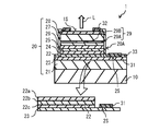
本開示の一実施の形態に係る面発光レーザ1について説明する。図1は、面発光レーザ1の断面構成例を表したものである。
[構成]
本開示の一実施の形態に係る面発光レーザ1について説明する。図1は、面発光レーザ1の断面構成例を表したものである。
面発光レーザ1は、基板10上に垂直共振器を備えている。垂直共振器は、基板10の法線方向において互いに対向する2つのDBR(distributed Bragg reflector)層(n型DBR層21、p型DBR層27)によって発振波長λ0で発振するように構成されている。n型DBR層21は、本開示の「第1DBR層」の一具体例に相当する。p型DBR層27は、本開示の「第2DBR層」の一具体例に相当する。n型DBR層21は、p型DBR層27と比べて基板10寄りの位置に形成されている。p型DBR層27は、n型DBR層21と比べて基板10から離れた位置に形成されている。面発光レーザ1は、p型DBR層27側からレーザ光Lが出射されるように構成されている。従って、面発光レーザ1は、上面にレーザ光Lの光出射面1Sを有する上面出射型のレーザである。
面発光レーザ1は、基板10上に、基板10を結晶成長基板としてエピタキシャル結晶成長法により形成されたエピタキシャル積層構造20を備えている。エピタキシャル積層構造20は、例えば、n型DBR層21、2次元電子ガス生成層22、n型コンタクト層23、スペーサ層24、活性層25、スペーサ層26、p型DBR層27およびp型コンタクト層28を、基板10側からこの順に含んで構成されている。n型コンタクト層23は、本開示の「第1導電型コンタクト層」の一具体例に相当する。p型コンタクト層28は、本開示の「第2導電型コンタクト層」の一具体例に相当する。
エピタキシャル積層構造20において、少なくとも、スペーサ層24、活性層25、スペーサ層26、p型DBR層27およびp型コンタクト層28は、基板10の法線方向に延在する柱状のメサ部20Aを構成している。2次元電子ガス生成層22およびn型コンタクト層23は、メサ部20Aとの位置関係で、n型DBR層21側の領域に設けられている。2次元電子ガス生成層22は、n型コンタクト層23を間にして、少なくとも、メサ部20Aおよび電極層31と対向する位置に設けられている。n型コンタクト層23は、2次元電子ガス生成層22よりも活性層25寄りの位置に形成されている。2次元電子ガス生成層22およびn型コンタクト層23は、n型DBR層21と活性層25との間に設けられている。基板10は、2次元電子ガス生成層22およびn型コンタクト層23を介して、メサ部20Aと対向する位置に配置されている。
面発光レーザ1は、メサ部20Aの頂部(つまり、p型コンタクト層28)に接する電極層32を備えており、メサ部20Aのすそ野に広がるn型コンタクト層23に接する電極層31を備えている。p型コンタクト層28は、p型DBR層27と電極層32とを互いにオーミック接触させるための層である。n型コンタクト層23は、電極層31とメサ部20Aの中心部分との間の電流経路となる層である。電極層32は、例えば、少なくとも、活性層25の発光領域と対向する位置に開口を有するリング形状となっている。n型コンタクト層23のうち、電極層32の開口内に露出している表面が光出射面1Sとなる。電極層31は、n型コンタクト層23の、活性層25側の表面のうち、メサ部20Aのすそ野に相当する箇所(つまり、メサ部20Aに被覆されずに露出している露出面)に接している。電極層32は、本開示の「第1電極層」の一具体例に相当する。電極層31は、本開示の「第2電極層」の一具体例に相当する。
面発光レーザ1は、例えば、砒化物半導体によって形成されている。砒化物半導体とは、砒素(As)元素を含み、またアルミニウム(Al)、ガリウム(Ga)、インジウム(In)のうちの少なくとも1元素以上を含んで構成された化合物半導体を指す。基板10は、例えば、n型半導体基板である。基板10に用いられ得るn型半導体基板としては、例えば、n型GaAs基板が挙げられる。基板10は、半絶縁性半導体基板であってもよい。基板10に用いられ得る半絶縁性半導体基板としては、例えば、GaAs基板が挙げられる。基板10は、活性層25から発せられた光の吸収を低減する観点からは、半絶縁性半導体基板であってもよい。基板10に用いられ得る半絶縁性半導体基板としては、例えば、半絶縁性GaAs基板が挙げられる。
n型DBR層21は、低屈折率層(図示せず)および高屈折率層(図示せず)を交互に積層して構成されたものである。n型DBR層21において、低屈折率層は例えば光学厚さがλ0×1/4(λ0は発振波長)のn型Alx1Ga1-x1As(0<x1<1)からなり、高屈折率層は例えば光学厚さがλ0×1/4のn型Alx2Ga1-x2As(0≦x2<x1)からなる。
2次元電子ガス生成層22は、半導体層内で2次元状に電子が分布する状態を生成可能に構成されている。2次元電子ガス生成層22は、例えば、積層された2種類の半導体層の境界で伝導帯に障壁を作り、電圧やドーピングの調整により、フェルミ準位が伝導帯より上に来るように構成されている。2次元電子ガス生成層22は、例えば、ノンドープGaAs層22c、ノンドープAlGaAs層22bおよびn型AlGaAs層22aをn型コンタクト層23側からこの順に含んで構成された積層体内に形成されている。2次元電子ガス生成層22は、例えば、n型DBR層21上に、n型AlGaAs層22a、ノンドープAlGaAs層22bおよびノンドープGaAs層22cをこの順に積層して構成された積層体内に形成されている。例えば、図1、図2に示したように、ノンドープGaAs層22cのうち、ノンドープGaAs層22cとノンドープAlGaAs層22bとの境界付近では、伝導帯に障壁が形成されており、フェルミ準位EFが伝導帯より上に来ている。従って、ノンドープGaAs層22cのうち、ノンドープGaAs層22cとノンドープAlGaAs層22bとの境界付近に、2次元電子ガス生成層22が形成されている。
n型コンタクト層23は、例えば、n型GaAsからなる。スペーサ層24は、例えばn型Alx3Ga1-x3As(0≦x3<1)からなる。n型DBR層21、n型AlGaAs層22a、n型コンタクト層23およびスペーサ層24におけるn型不純物としては、例えば、ケイ素(Si)が挙げられる。
活性層25は、例えば、アンドープのInx4Ga1-x4As(0<x4<1)からなる井戸層(図示せず)およびアンドープのAlx5Ga1-x5As(0≦x5<1)からなる障壁層(図示せず)を交互に積層してなる多重量子井戸構造となっている。なお、活性層25のうち電流注入領域29B(後述)との対向領域が発光領域となる。
スペーサ層26は、例えばp型Alx6Ga1-x6As(0≦x6<1)からなる。p型DBR層27は、低屈折率層(図示せず)および高屈折率層(図示せず)を交互に積層して構成されたものである。p型DBR層27において、低屈折率層は例えば光学厚さがλ0×1/4のp型Alx7Ga1-x7As(0<x7<1)からなり、高屈折率層は例えば光学厚さがλ0×1/4のn型Alx8Ga1-x8As(0≦x8<x7)からなる。p型DBR層27は、n型DBR層21と比較して、メサ部20A内の垂直共振器の発振波長λ0に対して小さな反射率を有するよう構成されている。p型DBR層27は、例えば、n型DBR層21と比較して薄く形成されている。p型コンタクト層28は、例えば、p型Alx9Ga1-x9As(0≦x9<1)からなる。スペーサ層26、p型DBR層27およびp型コンタクト層28におけるp型不純物としては、例えば、カーボン(C)が挙げられる。
エピタキシャル積層構造20は、p型DBR層27内、または、p型DBR層27とスペーサ層26との間に、電流狭窄層29を有している。電流狭窄層29は、電流注入領域29Bおよび電流狭窄領域29Aを有する。電流狭窄領域29Aは、電流注入領域29Bの周辺領域に形成されている。電流注入領域29Bは、例えばp型Alx10Ga1-x10As(0<x10≦1)からなる。電流狭窄領域29Aは、例えば、Al2O3(酸化アルミニウム)を含んで構成されており、例えば、後述のAlAs層に含まれる高濃度のAlを、側面から酸化することにより得られる。従って、電流狭窄層29は電流を狭窄する機能を有している。
電極層31は、n型コンタクト層23のうち、メサ部20A側の表面に接している。電極層31は、合金を含んで構成されており、例えば、AuGe、Ni、Auをn型コンタクト層23側から順に積層して構成された積層体となっている。電極層32は、非合金によって構成されており、例えば、Ti、Pt、Auをp型コンタクト層28側から順に積層して構成された積層体となっている。メサ部20Aの周囲には、絶縁層33が形成されている。絶縁層33は、メサ部20Aを保護するための層であり、例えば、SiO2またはSi3N4で構成されている。
[製造方法]
次に、本実施の形態に係る面発光レーザ1の製造方法について説明する。
次に、本実施の形態に係る面発光レーザ1の製造方法について説明する。
面発光レーザ1を製造するためには、例えばGaAsからなる基板10上に、化合物半導体を、例えばMOCVD(Metal Organic Chemical Vapor Deposition :有機金属気相成長)法などのエピタキシャル結晶成長法により一括に形成する。この際、化合物半導体の原料としては、例えば、トリメチルアルミニウム(TMAl)、トリメチルガリウム(TMGa)、トリメチルインジウム(TMIn)などのメチル系有機金属ガスと、アルシン(AsH3)ガスを用い、ドナー不純物の原料としては、例えばジシラン(Si2H6)を用い、アクセプタ不純物の原料としては、例えば四臭化炭素(CBr4)を用いる。
まず、基板10の表面上に、例えばMOCVD法などのエピタキシャル結晶成長法により、n型DBR層21、2次元電子ガス生成層22、n型コンタクト層23、スペーサ層24、活性層25、スペーサ層26、p型DBR層27およびp型コンタクト層28を含むエピタキシャル積層構造20を形成する。
次に、例えば、円形状のレジスト層(図示せず)を形成したのち、このレジスト層をマスクとして、エピタキシャル積層構造20を選択的にエッチングするとともに、n型コンタクト層23に達する深さまでエピタキシャル積層構造20をエッチングする。このとき、例えばCl系ガスによるRIE(Reactive Ion Etching)を用いることが好ましい。このようにして、柱状のメサ部20Aを形成する。このとき、メサ部20Aのすそ野には、n型コンタクト層23が露出している。また、電流狭窄層29が形成される箇所にAlAs層が形成されており、メサ部20Aの側面にはAlAs層が露出している。その後、レジスト層を除去する。
次に、水蒸気雰囲気中において、高温で酸化処理を行い、メサ部20Aの側面からAlAs層に含まれるAlを選択的に酸化する。または、ウエット酸化法により、メサ部20Aの側面からAlAs層に含まれるAlを選択的に酸化する。これにより、メサ部20A内において、AlAs層の外縁領域が絶縁層(酸化アルミニウム)となり、電流狭窄層29が形成される。
次に、メサ部20A(例えばp型コンタクト層28)の上面に接する電極層32を形成したのち、メサ部20Aを覆う絶縁層33を形成する。このとき、メサ部20Aのすそ野の所定の箇所に開口を形成しておく。次に、その開口内に、n型コンタクト層23のうち、メサ部20A側の表面(露出面)に接する電極層31を形成する。このようにして、面発光レーザ1が製造される。
[動作]
このような構成の面発光レーザ1では、n型コンタクト層23と電気的に接続された電極層31と、p型コンタクト層28と電気的に接続された電極層32との間に所定の電圧が印加されると、電流狭窄層29で狭窄された電流が活性層25に注入され、これにより電子と正孔の再結合による発光が生じる。その結果、メサ部20A内の垂直共振器により、発振波長λ0でレーザ発振が生じる。そして、p型DBR層27から漏れ出た光がビーム状のレーザ光Lとなって光出射面1Sから外部に出力される。
このような構成の面発光レーザ1では、n型コンタクト層23と電気的に接続された電極層31と、p型コンタクト層28と電気的に接続された電極層32との間に所定の電圧が印加されると、電流狭窄層29で狭窄された電流が活性層25に注入され、これにより電子と正孔の再結合による発光が生じる。その結果、メサ部20A内の垂直共振器により、発振波長λ0でレーザ発振が生じる。そして、p型DBR層27から漏れ出た光がビーム状のレーザ光Lとなって光出射面1Sから外部に出力される。
[効果]
次に、比較例と対比しつつ、本実施の形態に係る面発光レーザ1の効果について、説明する。
次に、比較例と対比しつつ、本実施の形態に係る面発光レーザ1の効果について、説明する。
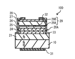
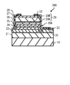
図3、図4は、比較例に係る面発光レーザ100,200の断面構成例を表したものである。図3に記載の面発光レーザ100では、電極層31が基板10の裏面に設けられている。この場合、基板10を例えばn型GaAs基板で構成し、メサ部20A上の電極層32と、基板10の裏面に設けられた電極層31との間に所定の電圧を印加することにより、レーザ発振が生じる。このとき、基板10およびn型DBR層21の厚さ方向の抵抗成分によって、駆動電圧が高くなる。
図4に記載の面発光レーザ200では、n型コンタクト層23が厚く形成されている。これにより、横方向の抵抗成分が低くなり、駆動電圧が低減される。しかし、n型コンタクト層23が厚く形成されていることから、n型コンタクト層23での光吸収が生じ、閾値電流が悪化し、光出力が低下する。
一方、本実施の形態では、電極層31に接するn型コンタクト層23によって、面発光レーザ1の駆動電圧が低減され、n型コンタクト層23の近くに設けられた2次元電子ガス生成層22によって、n型コンタクト層23を薄くした場合であっても、キャリアの輸送が確保される。n型コンタクト層23が薄く形成された場合、n型コンタクト層23での光吸収が抑制され、閾値電流が小さくなり、光出力が改善する。一方で、2次元電子ガス生成層22の存在により、横方向のキャリアの輸送が確保されるので、横方向の抵抗成分が低くなり、駆動電圧が低減される。従って、本実施の形態では、高光出力と低駆動電圧を両立することができる。
本実施の形態では、n型コンタクト層23が2次元電子ガス生成層22よりも活性層25寄りの位置に形成され、電極層31がn型コンタクト層23のうち、活性層25側の表面(露出面)に接する。これにより、製造過程において、エピタキシャル積層構造20を選択的にエッチングすることにより、メサ部20Aを形成すると同時に、n型コンタクト層23の露出面を形成することができる。従って、製造過程に特別な工程を設けなくても、高光出力と低駆動電圧を両立することができる。
本実施の形態では、2次元電子ガス生成層22が、ノンドープGaAs層22c、ノンドープAlGaAs層22bおよびn型AlGaAs層22aをn型コンタクト層23側からこの順に含んで構成されており、ノンドープGaAs層22cのうち、ノンドープGaAs層22cとノンドープAlGaAs層22bとの境界付近に、2次元電子ガス生成層22が形成されている。このように、ノンドープの層を用いて2次元電子ガス生成層22を形成することができるので、2次元電子ガス生成層22での光吸収が抑制され、閾値電流が小さくなり、光出力が改善する。従って、高光出力と低駆動電圧を両立することができる。
<変形例>
[変形例A]
上記実施の形態において、例えば、図5に示したように、2次元電子ガス生成層22とn型コンタクト層23の位置関係が入れ替わっていてもよい。このとき、2次元電子ガス生成層22は、n型コンタクト層23よりも活性層25寄りの位置に形成され、n型コンタクト層23は、活性層25側の表面のうち、メサ部20Aのすそ野に相当する箇所に、2次元電子ガス生成層22に被覆されずに露出する露出面2Sを有している。エピタキシャル積層構造20において、少なくとも、スペーサ層24、活性層25、スペーサ層26、p型DBR層27およびp型コンタクト層28は、基板10の法線方向に延在する柱状のメサ部20Aを構成している。なお、図5には、エピタキシャル積層構造20において、少なくとも、2次元電子ガス生成層22、スペーサ層24、活性層25、スペーサ層26、p型DBR層27およびp型コンタクト層28が、基板10の法線方向に延在する柱状のメサ部20Aを構成している場合が例示されている。
[変形例A]
上記実施の形態において、例えば、図5に示したように、2次元電子ガス生成層22とn型コンタクト層23の位置関係が入れ替わっていてもよい。このとき、2次元電子ガス生成層22は、n型コンタクト層23よりも活性層25寄りの位置に形成され、n型コンタクト層23は、活性層25側の表面のうち、メサ部20Aのすそ野に相当する箇所に、2次元電子ガス生成層22に被覆されずに露出する露出面2Sを有している。エピタキシャル積層構造20において、少なくとも、スペーサ層24、活性層25、スペーサ層26、p型DBR層27およびp型コンタクト層28は、基板10の法線方向に延在する柱状のメサ部20Aを構成している。なお、図5には、エピタキシャル積層構造20において、少なくとも、2次元電子ガス生成層22、スペーサ層24、活性層25、スペーサ層26、p型DBR層27およびp型コンタクト層28が、基板10の法線方向に延在する柱状のメサ部20Aを構成している場合が例示されている。
本変形例では、2次元電子ガス生成層22は、例えば、ノンドープGaAs層22c、ノンドープAlGaAs層22bおよびn型AlGaAs層22aをn型コンタクト層23側からこの順に含んで構成された積層体内に形成されている。2次元電子ガス生成層22は、例えば、n型コンタクト層23上に、ノンドープGaAs層22c、ノンドープAlGaAs層22bおよびn型AlGaAs層22aをこの順に積層して構成された積層体内に形成されている。本変形例では、例えば、図5、図6に示したように、ノンドープGaAs層22cのうち、ノンドープGaAs層22cとノンドープAlGaAs層22bとの境界付近では、伝導帯に障壁が形成されており、フェルミ準位EFが伝導帯より上に来ている。従って、ノンドープGaAs層22cのうち、ノンドープGaAs層22cとノンドープAlGaAs層22bとの境界付近に、2次元電子ガス生成層22が形成されている。
本変形例では、上記実施の形態と同様、電極層31に接するn型コンタクト層23によって、面発光レーザ1の駆動電圧が低減され、n型コンタクト層23の近くに設けられた2次元電子ガス生成層22によって、n型コンタクト層23を薄くした場合であっても、キャリアの輸送が確保される。n型コンタクト層23が薄く形成された場合、n型コンタクト層23での光吸収が抑制され、閾値電流が小さくなり、光出力が改善する。一方で、2次元電子ガス生成層22の存在により、横方向のキャリアの輸送が確保されるので、横方向の抵抗成分が低くなり、駆動電圧が低減される。従って、本変形例でも、高光出力と低駆動電圧を両立することができる。
本変形例では、2次元電子ガス生成層22がn型コンタクト層23よりも活性層25寄りの位置に形成され、電極層31がn型コンタクト層23のうち、メサ部20Aのすそ野に相当する箇所(つまり、2次元電子ガス生成層22に被覆されずに露出する露出面2S)に接する。これにより、製造過程において、エピタキシャル積層構造20を選択的にエッチングすることにより、メサ部20Aを形成すると同時に、n型コンタクト層23の露出面を形成することができる。従って、製造過程に特別な工程を設けなくても、高光出力と低駆動電圧を両立することができる。また、上記実施の形態と比べて、n型コンタクト層23を活性層25からより遠くに配置することができるので、n型コンタクト層23での光吸収をより抑制することができる。
[変形例B]
上記実施の形態およびその変形例において、2次元電子ガス生成層22およびn型コンタクト層23が、例えば、図7、図8に示したように、n型DBR層21内に設けられていてもよい。このようにした場合であっても、上記実施の形態およびその変形例と同様に、高光出力と低駆動電圧を両立することができる。
上記実施の形態およびその変形例において、2次元電子ガス生成層22およびn型コンタクト層23が、例えば、図7、図8に示したように、n型DBR層21内に設けられていてもよい。このようにした場合であっても、上記実施の形態およびその変形例と同様に、高光出力と低駆動電圧を両立することができる。
[変形例C]
上記実施の形態およびその変形例では、面発光レーザ1はメサ部20Aの上面からレーザ光Lを出射する上面出射型となっていたが、基板10側からレーザ光Lを出射する裏面出射型となっていてもよい。このとき、基板10が省略されてもよい。基板10は、例えば、基板10と、エピタキシャル積層構造20との間に、リフトオフ層を設けておき、リフトオフ層にレーザなどを照射することにより、基板10を剥離することが可能である。このように、基板10を剥離することにより、基板10による光吸収損失をなくすことができる。従って、高光出力と低駆動電圧を両立することができる。
上記実施の形態およびその変形例では、面発光レーザ1はメサ部20Aの上面からレーザ光Lを出射する上面出射型となっていたが、基板10側からレーザ光Lを出射する裏面出射型となっていてもよい。このとき、基板10が省略されてもよい。基板10は、例えば、基板10と、エピタキシャル積層構造20との間に、リフトオフ層を設けておき、リフトオフ層にレーザなどを照射することにより、基板10を剥離することが可能である。このように、基板10を剥離することにより、基板10による光吸収損失をなくすことができる。従って、高光出力と低駆動電圧を両立することができる。
[変形例D]
上記実施の形態およびその変形例では、エピタキシャル積層構造20においてメサ部20Aの頂部側に設けられた半導体層がp型半導体で構成され、エピタキシャル積層構造20において基板10側に設けられた半導体層がn型半導体で構成されていた。しかし、上記実施の形態およびその変形例において、エピタキシャル積層構造20においてメサ部20Aの頂部側に設けられた半導体層がn型半導体で構成され、エピタキシャル積層構造20において基板10側に設けられた半導体層がp型半導体で構成されていてもよい。
上記実施の形態およびその変形例では、エピタキシャル積層構造20においてメサ部20Aの頂部側に設けられた半導体層がp型半導体で構成され、エピタキシャル積層構造20において基板10側に設けられた半導体層がn型半導体で構成されていた。しかし、上記実施の形態およびその変形例において、エピタキシャル積層構造20においてメサ部20Aの頂部側に設けられた半導体層がn型半導体で構成され、エピタキシャル積層構造20において基板10側に設けられた半導体層がp型半導体で構成されていてもよい。
[変形例E]
上記実施の形態およびその変形例では、面発光レーザ1が、砒化物半導体によって形成されている場合が例示されていた。しかし、上記実施の形態およびその変形例において、面発光レーザ1は、例えば、窒素(N)、ホウ素(B)、アンチモン(Sb)、リン(P)を含むIII-V族半導体によって形成されていてもよい。
上記実施の形態およびその変形例では、面発光レーザ1が、砒化物半導体によって形成されている場合が例示されていた。しかし、上記実施の形態およびその変形例において、面発光レーザ1は、例えば、窒素(N)、ホウ素(B)、アンチモン(Sb)、リン(P)を含むIII-V族半導体によって形成されていてもよい。
例えば、上記実施の形態およびその変形例において、2次元電子ガス生成層22が、例えば、ノンドープGaN層、ノンドープAlGaN層およびn型AlGaN層をn型コンタクト層23側からこの順に含んで構成された積層体内に形成されていてもよい。このとき、例えば、ノンドープGaN層のうち、ノンドープGaN層とノンドープAlGaN層との境界付近では、伝導帯に障壁が形成されており、フェルミ準位が伝導帯より上に来ている。従って、ノンドープGaN層のうち、ノンドープGaN層とノンドープAlGaN層との境界付近に、2次元電子ガス生成層22が形成されている。従って、本変形例においても、上記実施の形態およびその変形例と同様、高光出力と低駆動電圧を両立することができる。
以上、実施の形態およびその変形例を挙げて本開示を説明したが、本開示は上記実施の形態等に限定されるものではなく、種々変形が可能である。なお、本明細書中に記載された効果は、あくまで例示である。本開示の効果は、本明細書中に記載された効果に限定されるものではない。本開示が、本明細書中に記載された効果以外の効果を持っていてもよい。
また、例えば、本開示は以下のような構成を取ることができる。
(1)
第1DBR(distributed Bragg reflector)層、活性層、第2DBR層および第1導電型コンタクト層をこの順に含み、さらに、前記第1DBR層と前記活性層との間、または、前記第1DBR層内に第2導電型コンタクト層および2次元電子ガス生成層を含む積層構造と、
前記第1導電型コンタクト層に接する第1電極層と、
前記第2導電型コンタクト層に接する第2電極層と
を備えた
面発光レーザ。
(2)
前記第2導電型コンタクト層は、前記2次元電子ガス生成層よりも前記活性層寄りの位置に形成され、
前記積層構造のうち、少なくとも、前記活性層、前記第2DBR層および前記第1導電型コンタクト層が柱状のメサ部となっており、
前記第2電極層は、前記第2導電型コンタクト層のうち、前記活性層側の表面に接する
(1)に記載の面発光レーザ。
(3)
前記2次元電子ガス生成層は、前記第2導電型コンタクト層よりも前記活性層寄りの位置に形成され、
前記積層構造のうち、少なくとも、前記活性層、前記第2DBR層および前記第1導電型コンタクト層が柱状のメサ部となっており、
前記第2導電型コンタクト層は、前記活性層側の表面のうち、前記メサ部のすそ野に相当する箇所に、前記2次元電子ガス生成層に被覆されずに露出する露出面を有し、
前記第2電極層は、前記前記露出面に接する
(1)に記載の面発光レーザ。
(4)
前記積層構造は、ノンドープGaAs層、ノンドープAlGaAs層および第2導電型AlGaAs層を前記第2導電型コンタクト層側からこの順に有し、
前記2次元電子ガス生成層は、前記ノンドープGaAs層のうち、前記ノンドープAlGaAs層と前記ノンドープAlGaAs層との境界付近に形成される
(1)ないし(3)のいずれか1つに記載の面発光レーザ。
(5)
前記積層構造は、ノンドープGaN層、ノンドープAlGaN層および第2導電型AlGaN層を前記第2導電型コンタクト層側からこの順に有し、
前記2次元電子ガス生成層は、前記ノンドープGaN層のうち、前記ノンドープAlGaN層と前記ノンドープAlGaN層との境界付近に形成される
(1)ないし(3)のいずれか1つに記載の面発光レーザ。
(1)
第1DBR(distributed Bragg reflector)層、活性層、第2DBR層および第1導電型コンタクト層をこの順に含み、さらに、前記第1DBR層と前記活性層との間、または、前記第1DBR層内に第2導電型コンタクト層および2次元電子ガス生成層を含む積層構造と、
前記第1導電型コンタクト層に接する第1電極層と、
前記第2導電型コンタクト層に接する第2電極層と
を備えた
面発光レーザ。
(2)
前記第2導電型コンタクト層は、前記2次元電子ガス生成層よりも前記活性層寄りの位置に形成され、
前記積層構造のうち、少なくとも、前記活性層、前記第2DBR層および前記第1導電型コンタクト層が柱状のメサ部となっており、
前記第2電極層は、前記第2導電型コンタクト層のうち、前記活性層側の表面に接する
(1)に記載の面発光レーザ。
(3)
前記2次元電子ガス生成層は、前記第2導電型コンタクト層よりも前記活性層寄りの位置に形成され、
前記積層構造のうち、少なくとも、前記活性層、前記第2DBR層および前記第1導電型コンタクト層が柱状のメサ部となっており、
前記第2導電型コンタクト層は、前記活性層側の表面のうち、前記メサ部のすそ野に相当する箇所に、前記2次元電子ガス生成層に被覆されずに露出する露出面を有し、
前記第2電極層は、前記前記露出面に接する
(1)に記載の面発光レーザ。
(4)
前記積層構造は、ノンドープGaAs層、ノンドープAlGaAs層および第2導電型AlGaAs層を前記第2導電型コンタクト層側からこの順に有し、
前記2次元電子ガス生成層は、前記ノンドープGaAs層のうち、前記ノンドープAlGaAs層と前記ノンドープAlGaAs層との境界付近に形成される
(1)ないし(3)のいずれか1つに記載の面発光レーザ。
(5)
前記積層構造は、ノンドープGaN層、ノンドープAlGaN層および第2導電型AlGaN層を前記第2導電型コンタクト層側からこの順に有し、
前記2次元電子ガス生成層は、前記ノンドープGaN層のうち、前記ノンドープAlGaN層と前記ノンドープAlGaN層との境界付近に形成される
(1)ないし(3)のいずれか1つに記載の面発光レーザ。
本開示の一実施形態に係る面発光レーザによれば、2電極層に接する第2導電型コンタクト層によって、面発光レーザの駆動電圧を低減し、第2導電型コンタクト層の近くに設けられた2次元電子ガス生成層によって、第2導電型コンタクト層を薄くした場合であっても、キャリアの輸送を確保できるようにしたので、高光出力と低駆動電圧を両立することができる。
本出願は、日本国特許庁において2020年3月19日に出願された日本特許出願番号第2020-048988号を基礎として優先権を主張するものであり、この出願のすべての内容を参照によって本出願に援用する。
当業者であれば、設計上の要件や他の要因に応じて、種々の修正、コンビネーション、サブコンビネーション、および変更を想到し得るが、それらは添付の請求の範囲やその均等物の範囲に含まれるものであることが理解される。
Claims (5)
- 第1DBR(distributed Bragg reflector)層、活性層、第2DBR層および第1導電型コンタクト層をこの順に含み、さらに、前記第1DBR層と前記活性層との間、または、前記第1DBR層内に第2導電型コンタクト層および2次元電子ガス生成層を含む積層構造と、
前記第1導電型コンタクト層に接する第1電極層と、
前記第2導電型コンタクト層に接する第2電極層と
を備えた
面発光レーザ。 - 前記第2導電型コンタクト層は、前記2次元電子ガス生成層よりも前記活性層寄りの位置に形成され、
前記積層構造のうち、少なくとも、前記活性層、前記第2DBR層および前記第1導電型コンタクト層が柱状のメサ部となっており、
前記第2電極層は、前記第2導電型コンタクト層のうち、前記活性層側の表面に接する
請求項1に記載の面発光レーザ。 - 前記2次元電子ガス生成層は、前記第2導電型コンタクト層よりも前記活性層寄りの位置に形成され、
前記積層構造のうち、少なくとも、前記活性層、前記第2DBR層および前記第1導電型コンタクト層が柱状のメサ部となっており、
前記第2導電型コンタクト層は、前記活性層側の表面のうち、前記メサ部のすそ野に相当する箇所に、前記2次元電子ガス生成層に被覆されずに露出する露出面を有し、
前記第2電極層は、前記前記露出面に接する
請求項1に記載の面発光レーザ。 - 前記積層構造は、ノンドープGaAs層、ノンドープAlGaAs層および第2導電型AlGaAs層を前記第2導電型コンタクト層側からこの順に有し、
前記2次元電子ガス生成層は、前記ノンドープGaAs層のうち、前記ノンドープAlGaAs層と前記ノンドープAlGaAs層との境界付近に形成される
請求項1に記載の面発光レーザ。 - 前記積層構造は、ノンドープGaN層、ノンドープAlGaN層および第2導電型AlGaN層を前記第2導電型コンタクト層側からこの順に有し、
前記2次元電子ガス生成層は、前記ノンドープGaN層のうち、前記ノンドープAlGaN層と前記ノンドープAlGaN層との境界付近に形成される
請求項1に記載の面発光レーザ。
Priority Applications (3)
| Application Number | Priority Date | Filing Date | Title |
|---|---|---|---|
| JP2022508265A JPWO2021187282A1 (ja) | 2020-03-19 | 2021-03-10 | |
| DE112021001755.1T DE112021001755T5 (de) | 2020-03-19 | 2021-03-10 | Oberflächenemittierender Laser |
| US17/906,182 US20230112925A1 (en) | 2020-03-19 | 2021-03-10 | Surface emitting laser |
Applications Claiming Priority (2)
| Application Number | Priority Date | Filing Date | Title |
|---|---|---|---|
| JP2020048988 | 2020-03-19 | ||
| JP2020-048988 | 2020-03-19 |
Publications (1)
| Publication Number | Publication Date |
|---|---|
| WO2021187282A1 true WO2021187282A1 (ja) | 2021-09-23 |
Family
ID=77771840
Family Applications (1)
| Application Number | Title | Priority Date | Filing Date |
|---|---|---|---|
| PCT/JP2021/009661 Ceased WO2021187282A1 (ja) | 2020-03-19 | 2021-03-10 | 面発光レーザ |
Country Status (4)
| Country | Link |
|---|---|
| US (1) | US20230112925A1 (ja) |
| JP (1) | JPWO2021187282A1 (ja) |
| DE (1) | DE112021001755T5 (ja) |
| WO (1) | WO2021187282A1 (ja) |
Families Citing this family (1)
| Publication number | Priority date | Publication date | Assignee | Title |
|---|---|---|---|---|
| CN119381893B (zh) * | 2024-12-30 | 2025-04-18 | 苏州长光华芯光电技术股份有限公司 | 一种高均匀性二维vcsel激光器及其制备方法 |
Citations (6)
| Publication number | Priority date | Publication date | Assignee | Title |
|---|---|---|---|---|
| JPH08204037A (ja) * | 1995-01-26 | 1996-08-09 | Nec Corp | 単一トラップメモリ装置 |
| JPH11135770A (ja) * | 1997-09-01 | 1999-05-21 | Sumitomo Chem Co Ltd | 3−5族化合物半導体とその製造方法および半導体素子 |
| JP2004031669A (ja) * | 2002-06-26 | 2004-01-29 | Seiko Epson Corp | 半導体素子部材及び半導体装置並びにそれらの製造方法、電気光学装置、電子機器 |
| JP2007324363A (ja) * | 2006-05-31 | 2007-12-13 | Ritsumeikan | 半導体装置 |
| US20150194789A1 (en) * | 2014-01-03 | 2015-07-09 | Finisar Corp | Vcsel with integrated electrically modulated intra-cavity graphene absorber |
| JP2018064061A (ja) * | 2016-10-14 | 2018-04-19 | 株式会社リコー | 半導体発光素子、照明装置、ヘッドライト、移動体、イルミネーション装置、映像装置、投射型映像装置及びプロジェクター。 |
Family Cites Families (7)
| Publication number | Priority date | Publication date | Assignee | Title |
|---|---|---|---|---|
| JPH1146038A (ja) | 1997-05-29 | 1999-02-16 | Nichia Chem Ind Ltd | 窒化物半導体レーザ素子及びその製造方法 |
| JP2002176226A (ja) * | 2000-09-22 | 2002-06-21 | Toshiba Corp | 光素子およびその製造方法 |
| US9136673B2 (en) * | 2012-07-20 | 2015-09-15 | The Regents Of The University Of California | Structure and method for the fabrication of a gallium nitride vertical cavity surface emitting laser |
| JP2018125404A (ja) | 2017-01-31 | 2018-08-09 | 株式会社リコー | 面発光レーザ素子 |
| CN106848838B (zh) * | 2017-04-06 | 2019-11-29 | 中国科学院半导体研究所 | 基于多孔DBR的GaN基VCSEL芯片及制备方法 |
| TWI793076B (zh) * | 2017-06-30 | 2023-02-21 | 晶元光電股份有限公司 | 半導體元件 |
| JP7363897B2 (ja) * | 2019-06-24 | 2023-10-18 | 住友電気工業株式会社 | 面発光レーザ |
-
2021
- 2021-03-10 WO PCT/JP2021/009661 patent/WO2021187282A1/ja not_active Ceased
- 2021-03-10 DE DE112021001755.1T patent/DE112021001755T5/de active Pending
- 2021-03-10 JP JP2022508265A patent/JPWO2021187282A1/ja active Pending
- 2021-03-10 US US17/906,182 patent/US20230112925A1/en active Pending
Patent Citations (6)
| Publication number | Priority date | Publication date | Assignee | Title |
|---|---|---|---|---|
| JPH08204037A (ja) * | 1995-01-26 | 1996-08-09 | Nec Corp | 単一トラップメモリ装置 |
| JPH11135770A (ja) * | 1997-09-01 | 1999-05-21 | Sumitomo Chem Co Ltd | 3−5族化合物半導体とその製造方法および半導体素子 |
| JP2004031669A (ja) * | 2002-06-26 | 2004-01-29 | Seiko Epson Corp | 半導体素子部材及び半導体装置並びにそれらの製造方法、電気光学装置、電子機器 |
| JP2007324363A (ja) * | 2006-05-31 | 2007-12-13 | Ritsumeikan | 半導体装置 |
| US20150194789A1 (en) * | 2014-01-03 | 2015-07-09 | Finisar Corp | Vcsel with integrated electrically modulated intra-cavity graphene absorber |
| JP2018064061A (ja) * | 2016-10-14 | 2018-04-19 | 株式会社リコー | 半導体発光素子、照明装置、ヘッドライト、移動体、イルミネーション装置、映像装置、投射型映像装置及びプロジェクター。 |
Also Published As
| Publication number | Publication date |
|---|---|
| JPWO2021187282A1 (ja) | 2021-09-23 |
| DE112021001755T5 (de) | 2023-01-05 |
| US20230112925A1 (en) | 2023-04-13 |
Similar Documents
| Publication | Publication Date | Title |
|---|---|---|
| KR102556555B1 (ko) | 다중 터널 접합을 구비한 vcsel 레이저 및 그 제조 방법 | |
| US5557627A (en) | Visible-wavelength semiconductor lasers and arrays | |
| US6754245B2 (en) | GaN series surface-emitting laser diode having spacer for effective diffusion of holes between p-type electrode and active layer, and method for manufacturing the same | |
| KR20040041730A (ko) | 전류 제한 구조를 갖는 반도체 광소자 | |
| CN211929898U (zh) | 垂直腔面发射激光器件 | |
| JP7795900B2 (ja) | 垂直共振器型発光素子 | |
| JP7685986B2 (ja) | 面発光レーザ | |
| US20060193361A1 (en) | Vertical cavity surface emitting laser device having a higher optical output power | |
| US20220393436A1 (en) | Vertical cavity light-emitting element and manufacturing method of the same | |
| JP7660552B2 (ja) | 発光デバイスおよび発光デバイスの製造方法 | |
| WO2021187282A1 (ja) | 面発光レーザ | |
| US7459719B2 (en) | Superlattice optical semiconductor device where each barrier layer has high content of group III elements in center portion and low content near well layer | |
| EP4084242B1 (en) | Light-emitting device | |
| JP7622039B2 (ja) | 面発光レーザ | |
| US20070127533A1 (en) | Long-wavelength vertical cavity surface emitting lasers having oxide aperture and method for manufacturing the same | |
| US20260018864A1 (en) | Vertical cavity surface emitting laser device and vertical cavity surface emitting laser device array | |
| US20240022040A1 (en) | Surface emitting laser and surface emitting laser array | |
| JP7413901B2 (ja) | 発光素子 | |
| JP4786202B2 (ja) | 半導体発光素子 | |
| WO2024190073A1 (ja) | 面発光レーザおよび面発光レーザアレイ | |
| JP2006253340A (ja) | 面発光レーザ素子およびその製造方法および面発光レーザアレイおよび電子写真システムおよび光通信システムおよび光インターコネクションシステム | |
| WO2024185436A1 (ja) | 面発光レーザ | |
| JP2007299895A (ja) | 面発光レーザ素子、それを備えた面発光レーザアレイ、面発光レーザ素子または面発光レーザアレイを備えた電子写真システム、面発光レーザ素子または面発光レーザアレイを備えた光インターコネクションシステムおよび面発光レーザ素子または面発光レーザアレイを備えた光通信システム | |
| JP2024092908A (ja) | 半導体レーザ素子 | |
| JP2007129012A (ja) | 光半導体素子 |
Legal Events
| Date | Code | Title | Description |
|---|---|---|---|
| 121 | Ep: the epo has been informed by wipo that ep was designated in this application |
Ref document number: 21771718 Country of ref document: EP Kind code of ref document: A1 |
|
| ENP | Entry into the national phase |
Ref document number: 2022508265 Country of ref document: JP Kind code of ref document: A |
|
| 122 | Ep: pct application non-entry in european phase |
Ref document number: 21771718 Country of ref document: EP Kind code of ref document: A1 |