WO2021187069A1 - 電磁波透過性金属光沢部材 - Google Patents
電磁波透過性金属光沢部材 Download PDFInfo
- Publication number
- WO2021187069A1 WO2021187069A1 PCT/JP2021/007661 JP2021007661W WO2021187069A1 WO 2021187069 A1 WO2021187069 A1 WO 2021187069A1 JP 2021007661 W JP2021007661 W JP 2021007661W WO 2021187069 A1 WO2021187069 A1 WO 2021187069A1
- Authority
- WO
- WIPO (PCT)
- Prior art keywords
- electromagnetic wave
- layer
- metallic luster
- indium oxide
- metal layer
- Prior art date
- Legal status (The legal status is an assumption and is not a legal conclusion. Google has not performed a legal analysis and makes no representation as to the accuracy of the status listed.)
- Ceased
Links
Images


Classifications
-
- C—CHEMISTRY; METALLURGY
- C23—COATING METALLIC MATERIAL; COATING MATERIAL WITH METALLIC MATERIAL; CHEMICAL SURFACE TREATMENT; DIFFUSION TREATMENT OF METALLIC MATERIAL; COATING BY VACUUM EVAPORATION, BY SPUTTERING, BY ION IMPLANTATION OR BY CHEMICAL VAPOUR DEPOSITION, IN GENERAL; INHIBITING CORROSION OF METALLIC MATERIAL OR INCRUSTATION IN GENERAL
- C23C—COATING METALLIC MATERIAL; COATING MATERIAL WITH METALLIC MATERIAL; SURFACE TREATMENT OF METALLIC MATERIAL BY DIFFUSION INTO THE SURFACE, BY CHEMICAL CONVERSION OR SUBSTITUTION; COATING BY VACUUM EVAPORATION, BY SPUTTERING, BY ION IMPLANTATION OR BY CHEMICAL VAPOUR DEPOSITION, IN GENERAL
- C23C28/00—Coating for obtaining at least two superposed coatings either by methods not provided for in a single one of groups C23C2/00 - C23C26/00 or by combinations of methods provided for in subclasses C23C and C25C or C25D
- C23C28/30—Coatings combining at least one metallic layer and at least one inorganic non-metallic layer
- C23C28/32—Coatings combining at least one metallic layer and at least one inorganic non-metallic layer including at least one pure metallic layer
-
- B—PERFORMING OPERATIONS; TRANSPORTING
- B32—LAYERED PRODUCTS
- B32B—LAYERED PRODUCTS, i.e. PRODUCTS BUILT-UP OF STRATA OF FLAT OR NON-FLAT, e.g. CELLULAR OR HONEYCOMB, FORM
- B32B15/00—Layered products comprising a layer of metal
- B32B15/04—Layered products comprising a layer of metal comprising metal as the main or only constituent of a layer, which is next to another layer of the same or of a different material
-
- B—PERFORMING OPERATIONS; TRANSPORTING
- B32—LAYERED PRODUCTS
- B32B—LAYERED PRODUCTS, i.e. PRODUCTS BUILT-UP OF STRATA OF FLAT OR NON-FLAT, e.g. CELLULAR OR HONEYCOMB, FORM
- B32B15/00—Layered products comprising a layer of metal
- B32B15/20—Layered products comprising a layer of metal comprising aluminium or copper
-
- B—PERFORMING OPERATIONS; TRANSPORTING
- B32—LAYERED PRODUCTS
- B32B—LAYERED PRODUCTS, i.e. PRODUCTS BUILT-UP OF STRATA OF FLAT OR NON-FLAT, e.g. CELLULAR OR HONEYCOMB, FORM
- B32B3/00—Layered products comprising a layer with external or internal discontinuities or unevennesses, or a layer of non-planar shape; Layered products comprising a layer having particular features of form
- B32B3/10—Layered products comprising a layer with external or internal discontinuities or unevennesses, or a layer of non-planar shape; Layered products comprising a layer having particular features of form characterised by a discontinuous layer, i.e. formed of separate pieces of material
-
- B—PERFORMING OPERATIONS; TRANSPORTING
- B32—LAYERED PRODUCTS
- B32B—LAYERED PRODUCTS, i.e. PRODUCTS BUILT-UP OF STRATA OF FLAT OR NON-FLAT, e.g. CELLULAR OR HONEYCOMB, FORM
- B32B3/00—Layered products comprising a layer with external or internal discontinuities or unevennesses, or a layer of non-planar shape; Layered products comprising a layer having particular features of form
- B32B3/10—Layered products comprising a layer with external or internal discontinuities or unevennesses, or a layer of non-planar shape; Layered products comprising a layer having particular features of form characterised by a discontinuous layer, i.e. formed of separate pieces of material
- B32B3/14—Layered products comprising a layer with external or internal discontinuities or unevennesses, or a layer of non-planar shape; Layered products comprising a layer having particular features of form characterised by a discontinuous layer, i.e. formed of separate pieces of material characterised by a face layer formed of separate pieces of material which are juxtaposed side-by-side
-
- B—PERFORMING OPERATIONS; TRANSPORTING
- B32—LAYERED PRODUCTS
- B32B—LAYERED PRODUCTS, i.e. PRODUCTS BUILT-UP OF STRATA OF FLAT OR NON-FLAT, e.g. CELLULAR OR HONEYCOMB, FORM
- B32B7/00—Layered products characterised by the relation between layers; Layered products characterised by the relative orientation of features between layers, or by the relative values of a measurable parameter between layers, i.e. products comprising layers having different physical, chemical or physicochemical properties; Layered products characterised by the interconnection of layers
- B32B7/02—Physical, chemical or physicochemical properties
- B32B7/025—Electric or magnetic properties
-
- B—PERFORMING OPERATIONS; TRANSPORTING
- B32—LAYERED PRODUCTS
- B32B—LAYERED PRODUCTS, i.e. PRODUCTS BUILT-UP OF STRATA OF FLAT OR NON-FLAT, e.g. CELLULAR OR HONEYCOMB, FORM
- B32B9/00—Layered products comprising a layer of a particular substance not covered by groups B32B11/00 - B32B29/00
-
- C—CHEMISTRY; METALLURGY
- C23—COATING METALLIC MATERIAL; COATING MATERIAL WITH METALLIC MATERIAL; CHEMICAL SURFACE TREATMENT; DIFFUSION TREATMENT OF METALLIC MATERIAL; COATING BY VACUUM EVAPORATION, BY SPUTTERING, BY ION IMPLANTATION OR BY CHEMICAL VAPOUR DEPOSITION, IN GENERAL; INHIBITING CORROSION OF METALLIC MATERIAL OR INCRUSTATION IN GENERAL
- C23C—COATING METALLIC MATERIAL; COATING MATERIAL WITH METALLIC MATERIAL; SURFACE TREATMENT OF METALLIC MATERIAL BY DIFFUSION INTO THE SURFACE, BY CHEMICAL CONVERSION OR SUBSTITUTION; COATING BY VACUUM EVAPORATION, BY SPUTTERING, BY ION IMPLANTATION OR BY CHEMICAL VAPOUR DEPOSITION, IN GENERAL
- C23C28/00—Coating for obtaining at least two superposed coatings either by methods not provided for in a single one of groups C23C2/00 - C23C26/00 or by combinations of methods provided for in subclasses C23C and C25C or C25D
- C23C28/30—Coatings combining at least one metallic layer and at least one inorganic non-metallic layer
- C23C28/34—Coatings combining at least one metallic layer and at least one inorganic non-metallic layer including at least one inorganic non-metallic material layer, e.g. metal carbide, nitride, boride, silicide layer and their mixtures, enamels, phosphates and sulphates
- C23C28/345—Coatings combining at least one metallic layer and at least one inorganic non-metallic layer including at least one inorganic non-metallic material layer, e.g. metal carbide, nitride, boride, silicide layer and their mixtures, enamels, phosphates and sulphates with at least one oxide layer
-
- B—PERFORMING OPERATIONS; TRANSPORTING
- B32—LAYERED PRODUCTS
- B32B—LAYERED PRODUCTS, i.e. PRODUCTS BUILT-UP OF STRATA OF FLAT OR NON-FLAT, e.g. CELLULAR OR HONEYCOMB, FORM
- B32B2255/00—Coating on the layer surface
- B32B2255/20—Inorganic coating
-
- B—PERFORMING OPERATIONS; TRANSPORTING
- B32—LAYERED PRODUCTS
- B32B—LAYERED PRODUCTS, i.e. PRODUCTS BUILT-UP OF STRATA OF FLAT OR NON-FLAT, e.g. CELLULAR OR HONEYCOMB, FORM
- B32B2307/00—Properties of the layers or laminate
- B32B2307/20—Properties of the layers or laminate having particular electrical or magnetic properties, e.g. piezoelectric
-
- B—PERFORMING OPERATIONS; TRANSPORTING
- B32—LAYERED PRODUCTS
- B32B—LAYERED PRODUCTS, i.e. PRODUCTS BUILT-UP OF STRATA OF FLAT OR NON-FLAT, e.g. CELLULAR OR HONEYCOMB, FORM
- B32B27/00—Layered products comprising a layer of synthetic resin
- B32B27/36—Layered products comprising a layer of synthetic resin comprising polyesters
-
- C—CHEMISTRY; METALLURGY
- C23—COATING METALLIC MATERIAL; COATING MATERIAL WITH METALLIC MATERIAL; CHEMICAL SURFACE TREATMENT; DIFFUSION TREATMENT OF METALLIC MATERIAL; COATING BY VACUUM EVAPORATION, BY SPUTTERING, BY ION IMPLANTATION OR BY CHEMICAL VAPOUR DEPOSITION, IN GENERAL; INHIBITING CORROSION OF METALLIC MATERIAL OR INCRUSTATION IN GENERAL
- C23C—COATING METALLIC MATERIAL; COATING MATERIAL WITH METALLIC MATERIAL; SURFACE TREATMENT OF METALLIC MATERIAL BY DIFFUSION INTO THE SURFACE, BY CHEMICAL CONVERSION OR SUBSTITUTION; COATING BY VACUUM EVAPORATION, BY SPUTTERING, BY ION IMPLANTATION OR BY CHEMICAL VAPOUR DEPOSITION, IN GENERAL
- C23C14/00—Coating by vacuum evaporation, by sputtering or by ion implantation of the coating forming material
- C23C14/06—Coating by vacuum evaporation, by sputtering or by ion implantation of the coating forming material characterised by the coating material
- C23C14/08—Oxides
- C23C14/086—Oxides of zinc, germanium, cadmium, indium, tin, thallium or bismuth
-
- C—CHEMISTRY; METALLURGY
- C23—COATING METALLIC MATERIAL; COATING MATERIAL WITH METALLIC MATERIAL; CHEMICAL SURFACE TREATMENT; DIFFUSION TREATMENT OF METALLIC MATERIAL; COATING BY VACUUM EVAPORATION, BY SPUTTERING, BY ION IMPLANTATION OR BY CHEMICAL VAPOUR DEPOSITION, IN GENERAL; INHIBITING CORROSION OF METALLIC MATERIAL OR INCRUSTATION IN GENERAL
- C23C—COATING METALLIC MATERIAL; COATING MATERIAL WITH METALLIC MATERIAL; SURFACE TREATMENT OF METALLIC MATERIAL BY DIFFUSION INTO THE SURFACE, BY CHEMICAL CONVERSION OR SUBSTITUTION; COATING BY VACUUM EVAPORATION, BY SPUTTERING, BY ION IMPLANTATION OR BY CHEMICAL VAPOUR DEPOSITION, IN GENERAL
- C23C14/00—Coating by vacuum evaporation, by sputtering or by ion implantation of the coating forming material
- C23C14/06—Coating by vacuum evaporation, by sputtering or by ion implantation of the coating forming material characterised by the coating material
- C23C14/14—Metallic material, boron or silicon
- C23C14/18—Metallic material, boron or silicon on other inorganic substrates
- C23C14/185—Metallic material, boron or silicon on other inorganic substrates by cathodic sputtering
Definitions
- the present invention relates to an electromagnetic wave transmitting metallic luster member.
- a member having electromagnetic wave transmission and metallic luster has both a high-class appearance derived from the metallic luster and electromagnetic wave transmission, and is therefore suitably used for an apparatus for transmitting and receiving electromagnetic waves.
- metal is used for the metallic luster member, the transmission and reception of electromagnetic waves is substantially impossible or hindered. Therefore, an electromagnetic wave-transmitting metallic luster member having both metallic luster and electromagnetic wave transmission is required so as not to interfere with the transmission and reception of electromagnetic waves and not to impair the design.
- Such an electromagnetic wave transmissive metal gloss member is used as a device for transmitting and receiving electromagnetic waves to various devices that require communication, for example, an electronic device such as a door handle of an automobile provided with a smart key, an in-vehicle communication device, a mobile phone, or a personal computer. It is expected to be applied to equipment and the like. Furthermore, in recent years, with the development of IoT technology, it is expected to be applied in a wide range of fields such as home appliances such as refrigerators and household appliances, which have not been used for communication in the past.
- Patent Document 1 includes an indium oxide-containing layer provided on the surface of a substrate and a metal layer laminated on the indium oxide-containing layer, and the metal layer is at least a part thereof. Describes an electromagnetically transmissive metallic luster member comprising a plurality of portions that are discontinuous with each other.
- the present invention has been made to solve the above problems in the prior art, and an object of the present invention is to provide an electromagnetic wave transmitting metallic luster member having high reflectance and exhibiting excellent electromagnetic wave transmission. do.
- the present invention is as follows. [1] A substrate, an indium oxide-containing layer continuously provided on the substrate, and a metal layer formed on the indium oxide-containing layer are provided.
- the metal layer contains a plurality of portions that are discontinuous with each other, at least in part.
- An electromagnetic wave-transmissive metallic luster member having a sheet resistance of the metal layer and the indium oxide-containing layer as a laminate of 2.50E + 8 ⁇ / ⁇ or more.
- an electromagnetic wave-transmitting metallic luster member having a high reflectance and exhibiting excellent electromagnetic wave transmission.
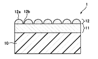
- FIG. 1 is a schematic cross-sectional view of an electromagnetic wave transmitting metallic luster member according to an embodiment of the present invention.
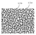
- FIG. 2 is a diagram showing an electron micrograph (SEM image) of the surface of an electromagnetic wave transmitting metallic luster member according to an embodiment of the present invention.
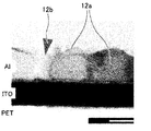
- FIG. 3 is a diagram showing an electron micrograph (TEM image) of a cross section of an electromagnetic wave transmitting metallic luster member according to an embodiment of the present invention.
- FIG. 4 is a diagram for explaining a method for measuring the thickness of the metal layer of the electromagnetic wave transmitting metallic luster member according to the embodiment of the present invention.
- FIG. 5 is a diagram showing the relationship between the film thickness of the indium oxide-containing layer and the sheet resistance of the electromagnetic wave transmitting metallic luster member in Examples and Comparative Examples of the present invention.
- the electromagnetic wave transmitting metal gloss member includes a substrate, an indium oxide-containing layer continuously provided on the substrate, and a metal layer formed on the indium oxide-containing layer.
- the metal layer contains a plurality of portions that are discontinuous with each other at least in part, and the sheet resistance of the metal layer and the indium oxide-containing layer as a laminate is 2.50E + 8 ⁇ / ⁇ or more. ..
- FIG. 1 shows a schematic cross-sectional view of an electromagnetic wave transmitting metallic luster member 1 according to an embodiment of the present invention.
- FIG. 2 shows an example of an electron micrograph (SEM image) of the surface of the electromagnetic wave transmitting metallic luster member 1 according to the embodiment of the present invention.
- the electromagnetic wave transmitting metallic luster member 1 includes a substrate 10, an indium oxide-containing layer 11 formed on the substrate 10, and a metal layer 12 formed on the indium oxide-containing layer 11. including.
- the indium oxide-containing layer 11 is provided on the surface of the substrate 10.
- the indium oxide-containing layer 11 may be provided directly on the surface of the substrate 10, or may be indirectly provided via a protective film or the like provided on the surface of the substrate 10.
- the indium oxide-containing layer 11 is preferably provided on the surface of the substrate 10 in a continuous state, in other words, without gaps.
- the metal layer 12 is laminated on the indium oxide-containing layer 11.
- the metal layer 12 includes a plurality of portions 12a. By being laminated on the indium oxide-containing layer 11, these portions 12a are separated from each other by a gap 12b at least in a discontinuous state, in other words, at least in a part. Since they are separated by the gap 12b, the sheet resistance of these portions 12a increases and the interaction with the radio waves decreases, so that the radio waves can be transmitted.
- Each of these portions 12a is an aggregate of sputtered particles formed by vapor deposition, sputtering, or the like of a metal. When the sputtered particles form a thin film on a substrate such as the substrate 10, the surface diffusivity of the particles on the substrate affects the shape of the thin film.
- the "discontinuous state” referred to in the present specification means a state in which they are separated from each other by a gap 12b, and as a result, they are electrically insulated from each other. By being electrically insulated, the sheet resistance is increased and the desired electromagnetic wave transmission can be obtained.
- the discontinuous form is not particularly limited, and includes, for example, islands, cracks, and the like.
- the “island” means that the particles, which are aggregates of sputtered particles, are each as shown in the electron micrograph (SEM image) of the surface of the metal layer of the electromagnetic wave transmitting metal gloss member in FIG. It is independent and means a structure in which the particles are spread so as to be slightly separated from each other or partially in contact with each other.
- the crack structure is a structure in which a metal thin film is divided by cracks.
- the metal layer 12 having a crack structure can be formed, for example, by providing a metal thin film layer on an indium oxide-containing layer formed on a substrate and bending and stretching the metal thin film layer to cause cracks in the metal thin film layer.
- the metal layer 12 having a crack structure can be easily formed by providing a brittle layer made of a material having poor elasticity, that is, easily forming cracks by stretching, between the indium oxide-containing layer and the metal thin film layer. can.
- the mode in which the metal layer 12 is discontinuous is not particularly limited, but from the viewpoint of productivity, it is preferably "island-shaped".
- Electromagnetic wave transmission The electromagnetic wave transmission of the metallic luster member 1 has a correlation with the sheet resistance.
- the sheet resistance of the metal layer of the electromagnetic wave transmitting metallic luster member 1 and the indium oxide-containing layer as a laminate must be 2.50E + 8 ⁇ / ⁇ or more.
- the amount of radio wave transmission attenuation in the microwave band (28 GHz) is , Less than 0.1 [ ⁇ dB].
- the amount of radio wave transmission attenuation in the microwave band (28 GHz) is preferably less than 10 [ ⁇ dB], more preferably less than 5 [ ⁇ dB], and even more preferably less than 2 [ ⁇ dB]. .. If the amount of radio wave transmission attenuation in the microwave band (28 GHz) is 10 [ ⁇ dB] or more, there is a problem that 90% or more of the radio waves are blocked.
- the sheet resistance of the electromagnetic wave transmitting metallic luster member 1 is preferably 1.00E + 10 ⁇ / ⁇ or more, and more preferably 1.00E + 12 ⁇ / ⁇ or more. If the electric resistance value is low, the leakage current may cause damage to the electric circuit or the like, and this can be prevented by increasing the resistance.
- the sheet resistance of the electromagnetic wave transmitting metallic luster member 1 can be measured by an eddy current measuring method according to JIS-Z2316-1: 2014.
- the sheet resistance of the electromagnetic wave transmitting metallic luster member 1 can be adjusted by adjusting the film thickness of the indium oxide-containing layer, the film thickness and the state of the metal layer, and the like.
- the amount of radio wave transmission attenuation and sheet resistance of the electromagnetic wave transmitting metallic luster member 1 are affected by the material and thickness of the indium oxide-containing layer 11 and the metal layer 12.
- the substrate 10 include resins, glasses, ceramics, and the like from the viewpoint of electromagnetic wave transmission.
- the substrate 10 may be a substrate film, a resin molded substrate, a glass substrate, or an article to which metallic luster should be imparted.
- the base film include polyethylene terephthalate (PET), polyethylene naphthalate (PEN), polybutylene terephthalate, polyamide, polyvinyl chloride, polycarbonate (PC), cycloolefin polymer (COP), and polystyrene.
- PET polyethylene terephthalate
- PEN polyethylene naphthalate
- PEN polybutylene terephthalate
- polyamide polyvinyl chloride
- PC polycarbonate
- COP cycloolefin polymer
- polystyrene Polypropylene
- PP Polypropylene
- polyethylene, polycycloolefin, polyurethane, acrylic (PMMA), ABS and other homopolymers and copolymers can be
- the layer 11 and the metal layer 12 can withstand high temperatures such as vapor deposition and sputtering. Therefore, among the above materials, for example, polyethylene terephthalate, polyethylene naphthalate, acrylic, polycarbonate, cycloolefin polymer, ABS, polypropylene, and polyurethane are preferable. Of these, polyethylene terephthalate, cycloolefin polymer, polycarbonate, and acrylic are preferable because they have a good balance between heat resistance and cost.
- the base film may be a single-layer film or a laminated film. From the viewpoint of ease of processing and the like, the thickness is preferably about 6 ⁇ m to 250 ⁇ m, for example. In order to strengthen the adhesive force with the indium oxide-containing layer 11 and the metal layer 12, plasma treatment, easy-adhesion treatment, or the like may be performed. Moreover, it is preferable that it does not contain particles.
- the base film is only an example of an object (base 10) on which the indium oxide-containing layer 11 can be formed.
- the substrate 10 includes a resin molded substrate, a glass substrate, and the article itself to which metallic luster should be imparted, in addition to the substrate film as described above.
- the resin molded base material and the articles to which the metallic luster should be imparted include vehicle structural parts, vehicle-mounted products, electronic device housings, home appliance housings, structural parts, mechanical parts, and various automobiles. Examples include parts for household appliances such as parts for electronic devices, furniture, kitchen utensils, medical equipment, parts for building materials, other structural parts and exterior parts.
- the indium oxide-containing layer 11 is formed on the substrate 10.
- the indium oxide-containing layer 11 may be provided directly on the surface of the substrate 10, or may be indirectly provided via a protective film or the like provided on the surface of the substrate 10.
- the indium oxide-containing layer 11 is preferably provided continuously on the surface of the substrate 10 to be imparted metallic luster, in other words, without gaps.
- the indium oxide-containing layer 11 is provided on the substrate 10, that is, the indium oxide-containing layer 11 is formed on the substrate 10, and the metal layer 12 described later is laminated on the indium oxide-containing layer 11. It becomes easy to form the metal layer 12 in a discontinuous state.
- the details of the mechanism are not always clear, but when sputtered particles by metal deposition or sputtering form a thin film on the substrate, the surface diffusivity of the particles on the substrate affects the shape of the thin film, and the substrate It is considered that the higher the temperature of the metal layer and the smaller the wettability of the metal layer with respect to the substrate, the easier it is to form a discontinuous structure. Then, it is considered that by providing the indium oxide-containing layer on the substrate, the surface diffusivity of the metal particles on the surface thereof is promoted, and the metal layer can be easily grown in a discontinuous state.
- the indium oxide-containing layer 11 can contain a metal-containing substance such as indium oxide (In 2 O 3 ), indium tin oxide (ITO), and indium zinc oxide (IZO).
- a metal-containing substance such as indium oxide (In 2 O 3 ), indium tin oxide (ITO), and indium zinc oxide (IZO).
- ITO indium tin oxide
- IZO indium zinc oxide
- the metal layer 12 is preferable because it tends to have an island-like discontinuous structure, for example. Further, in this case, not only tin (Sn) or indium (In) but also various metals such as aluminum, which are usually difficult to form a discontinuous structure and are difficult to apply for this application, are applied to the metal layer 12. It will be easier to include.
- the thickness of the indium oxide-containing layer 11 is preferably 4.6 nm or less, more preferably 4.4 nm or less, and further preferably 4.0 nm or less in order to improve the sheet resistance and electromagnetic wave transmission.
- the thickness is preferably 3.3 nm or more, more preferably 3.5 nm or more. It is more preferably 8 nm or more.
- the sheet resistance of the electromagnetic wave transmitting metallic luster member can be easily set to 2.50E + 8 ⁇ / ⁇ or more. As a result, it is easy to obtain an electromagnetic wave-transmitting metallic luster member showing high reflectance and having excellent electromagnetic wave transmission.
- the metal layer 12 is formed on the indium oxide-containing layer 11.
- the metal layer 12 is a layer having a metallic appearance, and is preferably a layer having a metallic luster.
- the material forming the metal layer 12 is not particularly limited, and may contain a metal or a resin, or may contain a metal and a resin.
- the thickness of the metal layer 12 in the electromagnetic wave transmitting metallic luster member according to the embodiment of the present invention is not particularly limited as long as the sheet resistance can be 2.50E + 8 ⁇ / ⁇ or more, and is, for example, in a wide range of 10 nm to 200 nm. Can be set. Within this range, the yield is improved and stable production is possible.
- the thickness of the metal layer 12 is preferably 10 nm or more from the viewpoint of exhibiting sufficient metallic luster, while it is preferably 200 nm or less from the viewpoint of sheet resistance and electromagnetic wave transmission.
- the thickness of the metal layer 12 is more preferably 10 nm to 100 nm, further preferably 10 nm to 70 nm. This thickness is also suitable for forming a uniform film with high productivity and obtaining an electromagnetic wave transmitting metallic luster member having high reflectance.
- the metal layer 12 is formed on the indium oxide-containing layer 11 and contains a plurality of portions that are discontinuous with each other at least in part.
- the metal layer 12 is in a continuous state on the indium oxide-containing layer 11, a sufficient metallic luster can be obtained, but the amount of radio wave transmission attenuation becomes very large, and therefore electromagnetic wave transmission cannot be ensured.
- the metal layer 12 has a relatively low melting point as well as being able to exhibit sufficient brilliance. This is because the metal layer 12 is preferably formed by thin film growth using sputtering. For this reason, a metal having a melting point of about 1100 ° C. or lower is suitable as the metal layer 12, and for example, aluminum (Al), zinc (Zn), lead (Pb), copper (Cu), and silver (Ag). ), And any of an alloy containing the metal as a main component is preferably contained. In particular, it is more preferable that the metal layer 12 contains aluminum or an aluminum alloy because of the brilliance, stability, price, and the like of the substance. When an aluminum alloy is used, the aluminum content is preferably 50% by mass or more.
- the equivalent circle diameter of the portion 12a of the metal layer 12 is not particularly limited, but is usually about 10 to 1000 nm.
- the average particle size of the plurality of portions 12a means the average value of the equivalent circle diameters of the plurality of portions 12a.
- the circle-equivalent diameter of the portion 12a is the diameter of a perfect circle corresponding to the area of the portion 12a.
- the distance between the portions 12a is not particularly limited, but is usually about 10 to 1000 nm.
- the electromagnetic wave transmitting metallic luster member 1 may be provided with other layers depending on the application, in addition to the above-mentioned indium oxide-containing layer 11 and the metal layer 12.
- Other layers include an optical adjustment layer (color adjustment layer) such as a high-refractive material for adjusting the appearance such as color, and a protective layer (scratch resistance layer) for improving durability such as scratch resistance.
- Barrier layer corrosion resistant layer
- easy-adhesion layer hard coat layer
- antireflection layer light extraction layer
- anti-glare layer and the like.
- the indium oxide-containing layer 11 is formed on the substrate 10 by vacuum vapor deposition, sputtering, ion plating or the like prior to the formation of the metal layer 12.
- sputtering is preferable because the thickness can be strictly controlled even in a large area.
- the metal target containing indium as a main component is not particularly limited, and for example, tin (Sn), zinc (Zn), or the like may be contained in addition to indium. good.
- the "main component” means the component having the highest content ratio (mass basis) among all the components in the metal target.
- Indium is preferably contained in the metal target in an amount of 70% by mass or more, more preferably 90% by mass or more.
- tin (Sn) When tin (Sn) is contained, it is preferably contained in the metal target in an amount of, for example, 2.5 to 30% by mass, more preferably 3 to 10% by mass. When zinc (Zn) is contained, for example, it is preferably contained in the metal target in an amount of 2 to 20% by mass, more preferably 5 to 15% by mass.
- the inert gas an inert gas such as argon or nitrogen is usually used. Further, a reactive gas such as oxygen gas can be used in combination.
- the power supply used for sputtering may be, for example, any of a DC power supply, an AC power supply, an MF power supply, and an RF power supply, or a combination thereof.
- the indium oxide-containing layer formed as described above preferably contains an indium oxide such as indium oxide (In 2 O 3 ), indium tin oxide (ITO), and indium zinc oxide (IZO).
- an indium oxide such as indium oxide (In 2 O 3 ), indium tin oxide (ITO), and indium zinc oxide (IZO).
- the metal layer 12 is laminated on the indium oxide-containing layer 11.
- methods such as vacuum deposition and sputtering can be used. It is preferable that the indium oxide-containing layer 11 and the metal layer 12 are in direct contact with each other without interposing another layer.
- electromagnetic wave transmissive metallic luster members Since the electromagnetic wave-transmitting metallic luster member of the present embodiment has electromagnetic wave transmission, it is preferable to use it for a device or an article for transmitting and receiving electromagnetic waves, its parts, and the like.
- applications for household goods such as structural parts for vehicles, vehicle-mounted products, housings for electronic devices, housings for home appliances, structural parts, mechanical parts, various automobile parts, electronic device parts, furniture, kitchen supplies, etc. , Medical equipment, building material parts, other structural parts, exterior parts, etc.
- ECU box electrical components, engine peripheral parts, drive system / gear peripheral parts, intake / exhaust system parts, cooling system parts, etc.
- home appliances such as refrigerators, washing machines, vacuum cleaners, microwave ovens, air conditioners, lighting equipment, electric water heaters, TVs, watches, ventilation fans, projectors, speakers, personal computers, mobile phones , Smartphones, digital cameras, tablet PCs, portable music players, portable game machines, chargers, electronic information devices such as batteries, and the like.
- Sheet resistance ( ⁇ / ⁇ ) as a laminate of a metal layer and an indium oxide-containing layer by eddy current measurement method using Hiresta (Highrester-UP MCP-HT450 device manufactured by Mitsubishi Chemical Analytech Co., Ltd.) and conforming to JIS-Z2316. ) was measured.
- a measurement terminal was pressed from the metal layer side of the base material, and a applied voltage of 1000 V was used to measure the sheet resistance (resistance value) when measured for 30 seconds. If the measured value can not be measured at 1000V (1.00 ⁇ 10 8 ⁇ / ⁇ or less) was measured sheet resistance (resistance value) by changing the applied voltage to the 100 V.
- ⁇ Reflectance> Using a spectrophotometer (U-4100 device manufactured by Hitachi High-Technologies Corporation), a light-shielding black acrylic plate was attached to the transparent substrate side of the film via an adhesive to prepare a sample for evaluation. Next, the value of the visual reflectance Y of the metal layer surface was measured under the condition of 5 ° specular reflection (wavelength: 380 nm to 780 nm).
- FIG. 3 shows an example of an electron micrograph (TEM image) of a cross section of an electromagnetic wave transmitting metallic luster member. In determining the maximum thickness, first, in the metal layer appearing on the surface of the electromagnetic wave transmitting metallic luster member as shown in FIG.
- a square region 3 having a side of 5 cm as shown in FIG. 4 is appropriately extracted, and the square region 3 is appropriately extracted.
- a total of five points "a” to "e” obtained by dividing the center lines A and B of the vertical and horizontal sides of the square region 3 into four equal parts were selected as measurement points.
- a viewing angle region including approximately five portions 12a was extracted. Approximately 5 parts 12a at each of these 5 measurement points, that is, the individual thicknesses (nm) of 25 (5 x 5) parts 12a were obtained, and the average value thereof was set to "maximum". "Thickness".
- ⁇ Thickness of indium oxide-containing layer> A sample in which the indium oxide-containing layer was adjusted for each thickness was prepared, and a transmission electron micrograph (TEM image) was measured with respect to the net peak intensity measured by the scanning fluorescence X-ray analyzer ZSX Primus II, and oxidation was performed. The thickness of the indium-containing layer was calculated, and a calibration curve of the thickness with respect to the net peak intensity was prepared. The thickness of the indium oxide-containing layer was calculated from the net peak intensity of fluorescent X-rays using the calibration curve. The average value thereof was calculated and used as the thickness of the indium oxide-containing layer (ITO film thickness (nm)).
- Example 1 As the base film, a PET film (thickness 50 ⁇ m) on which a particle-free hard coat layer was formed was used, and MF-AC magnetron sputtering was used to have a thickness of 4.4 nm along the surface of the base film.
- the ITO layer was formed directly on the ITO layer.
- the temperature of the base film when forming the ITO layer was set to 90 ° C.
- an aluminum (Al) layer having a thickness of 34.5 nm was formed on the ITO layer by using alternating current sputtering (MF-AC: 40 kHz) to obtain a metallic luster article (metal thin film).
- the obtained aluminum layer was a discontinuous layer.
- the temperature of the base film when forming the Al layer was set to 90 ° C.
- Example 2 to 4 In Examples 2 to 4, the thickness of the ITO layer in Example 1 was changed to 4.1 nm, 3.8 nm, 3.4 nm, and the thickness of the Al layer was changed to 34.5 nm, 33.1 nm, and 35.1 nm, respectively. A film was formed in the same manner.
- Comparative Example 1 In Comparative Example 1, the film was formed in the same manner except that the thickness of the ITO layer in Example 1 was changed to 3.2 nm. The thickness of Al was 32.7 nm.
- Comparative Examples 2 to 5 the thickness of the ITO layer in Example 1 was 2.5 nm, 5.2 nm, 6.1 nm, and 8.1 nm, respectively, and the thickness of the Al layer was 32.5 nm, 36.9 nm, and 29.1 nm, respectively.
- the film was formed in the same manner except that the thickness was changed to 29.1 nm.
- a PET film (thickness 50 ⁇ m) on which a hard coat layer containing no particles was formed was used.
- DC magnetron sputtering was used to directly form an ITO layer with a thickness of 4.8 nm along the surface of the substrate film.
- the temperature of the base film when forming the ITO layer was set to 130 ° C.
- an aluminum (Al) layer having a thickness of 38.0 nm was formed on the ITO layer to obtain a metallic luster article (metal thin film).
- the obtained aluminum layer was a discontinuous layer.
- the temperature of the base film when forming the Al layer was set to 130 ° C.
- FIG. 5 shows a diagram showing the relationship between the film thickness (nm) of the indium oxide-containing layer and the sheet resistance (resistance value ⁇ / ⁇ ).
- the sheet resistance was 2.50E + 8 ⁇ / ⁇ or more, and excellent electromagnetic wave transmission was exhibited.
- the reflectance was also sufficient. It is considered that this is because the formation of the metal layer having an island-like discontinuous structure was promoted.
- the laminated members of Comparative Examples 1 to 6 had lower sheet resistance and inferior electromagnetic wave transmission as compared with Examples. It is considered that this is because the resistance values of Comparative Examples 1 and 2 are very small, the thickness of the ITO layer is thin, and the island shape cannot be sufficiently formed, so that the low resistance derived from the metal layer appears.
- the resistance is not as low as that of Comparative Examples 1 and 2, but the value is smaller than 2.50E + 8 ⁇ / ⁇ . This is because the ITO layer is thick, so that the island shape is sufficiently formed, but it is considered that the resistance value derived from the ITO layer appears.
- metals other than aluminum (Al) particularly used in the above examples metals having a relatively low melting point such as zinc (Zn), lead (Pb), copper (Cu), and silver (Ag) are used. It is considered that a discontinuous structure can be formed by the same method.
- the electromagnetic wave-transmissive metallic luster member according to the present invention can be used for devices and articles that transmit and receive electromagnetic waves, parts thereof, and the like.
- applications for household goods such as structural parts for vehicles, vehicle-mounted products, housings for electronic devices, housings for home appliances, structural parts, mechanical parts, various automobile parts, electronic device parts, furniture, kitchen supplies, etc. It can also be used for various applications that require both design and electromagnetic wave transmission, such as medical equipment, building material parts, other structural parts and exterior parts.
- Electromagnetic wave transmissive metallic luster member 10 Base 11 Indium oxide-containing layer 12 Metal layer 12a Part 12b Gap
Landscapes
- Chemical & Material Sciences (AREA)
- Inorganic Chemistry (AREA)
- Chemical Kinetics & Catalysis (AREA)
- Engineering & Computer Science (AREA)
- Materials Engineering (AREA)
- Mechanical Engineering (AREA)
- Metallurgy (AREA)
- Organic Chemistry (AREA)
- Laminated Bodies (AREA)
Abstract
本発明は、基体と、前記基体上に連続状態で設けられた酸化インジウム含有層と、前記酸化インジウム含有層上に形成された金属層と、を備え、前記金属層は少なくとも一部において互いに不連続の状態にある複数の部分を含んでおり、前記金属層と前記酸化インジウム含有層の積層体としてのシート抵抗が、2.50E+8Ω/□以上である、電磁波透過性金属光沢部材に関する。
Description
本発明は、電磁波透過性金属光沢部材に関する。
従来、電磁波透過性及び金属光沢を有する部材が、その金属光沢に由来する外観の高級感と、電磁波透過性とを兼ね備えることから、電磁波を送受信する装置に好適に用いられている。
金属光沢調の部材に金属を使用した場合には、電磁波の送受信が実質的に不可能または妨害されてしまう。したがって、電磁波の送受信を妨げることなく、意匠性を損なわせないために、金属光沢と電磁波透過性の双方を兼ね備えた電磁波透過性金属光沢部材が必要とされている。
金属光沢調の部材に金属を使用した場合には、電磁波の送受信が実質的に不可能または妨害されてしまう。したがって、電磁波の送受信を妨げることなく、意匠性を損なわせないために、金属光沢と電磁波透過性の双方を兼ね備えた電磁波透過性金属光沢部材が必要とされている。
このような電磁波透過性金属光沢部材は、電磁波を送受信する装置として、通信を必要とする様々な機器、例えば、スマートキーを設けた自動車のドアハンドル、車載通信機器、携帯電話、パソコン等の電子機器等への応用が期待されている。更に、近年では、IoT技術の発達に伴い、従来は通信等行われることがなかった、冷蔵庫等の家電製品、生活機器等、幅広い分野での応用も期待されている。
電磁波透過性金属光沢部材に関して、特許文献1には、基体の面に設けた酸化インジウム含有層と、前記酸化インジウム含有層に積層された金属層と、を備え、前記金属層は、少なくとも一部において互いに不連続の状態にある複数の部分を含むことを特徴とする電磁波透過性金属光沢部材が記載されている。
従来技術の電磁波透過性金属光沢部材における金属層は、厚みを厚くすると反射率が高くなり、金属光沢が得やすくなる。しかし、金属層の厚みを厚くすると島状に形成された金属同士が重なり合ってしまい、抵抗値が急激に低下するため、電磁波透過性が著しく損なわれてしまう。そのため、反射率と電磁波透過性とはトレードオフの関係にあった。
本発明は、従来技術における上記問題を解決するためになされたものであり、高い反射率を有し、かつ、優れた電磁波透過性を示す、電磁波透過性金属光沢部材を提供することを目的とする。
本発明は、従来技術における上記問題を解決するためになされたものであり、高い反射率を有し、かつ、優れた電磁波透過性を示す、電磁波透過性金属光沢部材を提供することを目的とする。
本発明者等は、上記課題を解決するために鋭意検討を重ねた結果、シート抵抗を特定範囲とすることにより、上記課題を解決できることを見出し、本発明を完成するに至った。
すなわち、本発明は以下のとおりである。
〔1〕
基体と、前記基体上に連続状態で設けられた酸化インジウム含有層と、前記酸化インジウム含有層上に形成された金属層と、を備え、
前記金属層は少なくとも一部において互いに不連続の状態にある複数の部分を含んでおり、
前記金属層と前記酸化インジウム含有層の積層体としてのシート抵抗が、2.50E+8Ω/□以上である、電磁波透過性金属光沢部材。
〔2〕
前記酸化インジウム含有層の厚さは、3.3nm~4.6nmである、〔1〕に記載の電磁波透過性金属光沢部材。
〔3〕
前記酸化インジウム含有層が、酸化インジウム(In2O3)、インジウム錫酸化物(ITO)、又はインジウム亜鉛酸化物(IZO)のいずれかを含む、〔1〕または〔2〕に記載の電磁波透過性金属光沢部材。
〔4〕
前記金属層が、アルミニウム又はアルミニウム合金を含有する層である、〔1〕~〔3〕のいずれか1項に記載の電磁波透過性金属光沢部材。
〔5〕
前記金属層の厚さは、10nm~200nmである、〔1〕~〔4〕のいずれか1項に記載の電磁波透過性金属光沢部材。
〔6〕
前記複数の部分が島状に形成されている、〔1〕~〔5〕のいずれか1項に記載の電磁波透過性金属光沢部材。
〔7〕
前記基体が、基材フィルム、樹脂成型物基材、ガラス基材、又は金属光沢を付与すべき物品のいずれかである、〔1〕~〔6〕のいずれか1項に記載の電磁波透過性金属光沢部材。
〔1〕
基体と、前記基体上に連続状態で設けられた酸化インジウム含有層と、前記酸化インジウム含有層上に形成された金属層と、を備え、
前記金属層は少なくとも一部において互いに不連続の状態にある複数の部分を含んでおり、
前記金属層と前記酸化インジウム含有層の積層体としてのシート抵抗が、2.50E+8Ω/□以上である、電磁波透過性金属光沢部材。
〔2〕
前記酸化インジウム含有層の厚さは、3.3nm~4.6nmである、〔1〕に記載の電磁波透過性金属光沢部材。
〔3〕
前記酸化インジウム含有層が、酸化インジウム(In2O3)、インジウム錫酸化物(ITO)、又はインジウム亜鉛酸化物(IZO)のいずれかを含む、〔1〕または〔2〕に記載の電磁波透過性金属光沢部材。
〔4〕
前記金属層が、アルミニウム又はアルミニウム合金を含有する層である、〔1〕~〔3〕のいずれか1項に記載の電磁波透過性金属光沢部材。
〔5〕
前記金属層の厚さは、10nm~200nmである、〔1〕~〔4〕のいずれか1項に記載の電磁波透過性金属光沢部材。
〔6〕
前記複数の部分が島状に形成されている、〔1〕~〔5〕のいずれか1項に記載の電磁波透過性金属光沢部材。
〔7〕
前記基体が、基材フィルム、樹脂成型物基材、ガラス基材、又は金属光沢を付与すべき物品のいずれかである、〔1〕~〔6〕のいずれか1項に記載の電磁波透過性金属光沢部材。
本発明によれば、高い反射率を有し、かつ、優れた電磁波透過性を示す、電磁波透過性金属光沢部材を提供することができる。
以下、添付図面を参照しつつ、本発明を詳細に説明するが、本発明は以下の実施形態に限定されるものではなく、本発明の要旨を逸脱しない範囲において、任意に変形して実施できる。また、数値範囲を示す「~」とは、その前後に記載された数値を下限値及び上限値として含む意味で使用される。
<1.基本構成>
本発明の実施形態にかかる電磁波透過性金属光沢部材は、基体と、前記基体上に連続状態で設けられた酸化インジウム含有層と、前記酸化インジウム含有層上に形成された金属層と、を備え、前記金属層は少なくとも一部において互いに不連続の状態にある複数の部分を含んでおり、前記金属層と前記酸化インジウム含有層の積層体としてのシート抵抗が、2.50E+8Ω/□以上である。
本発明の実施形態にかかる電磁波透過性金属光沢部材は、基体と、前記基体上に連続状態で設けられた酸化インジウム含有層と、前記酸化インジウム含有層上に形成された金属層と、を備え、前記金属層は少なくとも一部において互いに不連続の状態にある複数の部分を含んでおり、前記金属層と前記酸化インジウム含有層の積層体としてのシート抵抗が、2.50E+8Ω/□以上である。
図1に、本発明の一実施形態による電磁波透過性金属光沢部材1の概略断面図を示す。また、図2に、本発明の一実施形態による電磁波透過性金属光沢部材1の表面の電子顕微鏡写真(SEM画像)の一例を示す。
図1に示すように、電磁波透過性金属光沢部材1は、基体10と、基体10の上に形成された酸化インジウム含有層11と、酸化インジウム含有層11の上に形成された金属層12とを含む。
酸化インジウム含有層11は、基体10の面に設けられている。酸化インジウム含有層11は、基体10の面に直接設けられていてもよいし、基体10の面に設けた保護膜等を介して間接的に設けられてもよい。酸化インジウム含有層11は、基体10の面に連続状態で、言い換えれば、隙間なく、設けるのが好ましい。連続状態で設けることにより、酸化インジウム含有層11、ひいては、電磁波透過性金属光沢部材1の平滑性や耐食性を向上させることができ、また、酸化インジウム含有層11を面内にばらつきなく成膜することも容易となる。
金属層12は酸化インジウム含有層11に積層される。金属層12は複数の部分12aを含む。酸化インジウム含有層11に積層されることにより、これらの部分12aは、少なくとも一部において互いに不連続の状態、言い換えれば、少なくとも一部において隙間12bによって隔てられる。隙間12bによって隔てられるため、これらの部分12aのシート抵抗は大きくなり、電波との相互作用が低下するため、電波を透過させることができる。これらの各部分12aは金属を蒸着、スパッタ等することによって形成されたスパッタ粒子の集合体である。スパッタ粒子が基体10等の基体上で薄膜を形成する際には、基体上での粒子の表面拡散性が薄膜の形状に影響を及ぼす。
なお、本明細書でいう「不連続の状態」とは、隙間12bによって互いに隔てられており、この結果、互いに電気的に絶縁されている状態を意味する。電気的に絶縁されることにより、シート抵抗が大きくなり、所望とする電磁波透過性が得られることになる。不連続の形態は、特に限定されるものではなく、例えば、島状、クラック等が含まれる。
ここで「島状」とは、図2の電磁波透過性金属光沢部材の金属層の表面の電子顕微鏡写真(SEM画像)に示されているように、スパッタ粒子の集合体である粒子同士が各々独立しており、それらの粒子が、互いに僅かに離間し又は一部接触した状態で敷き詰められてなる構造を意味する。
また、クラック構造とは、金属薄膜がクラックにより分断された構造である。
クラック構造の金属層12は、例えば基体上に形成した酸化インジウム含有層上に、金属薄膜層を設け、屈曲延伸して金属薄膜層にクラックを生じさせることにより形成することができる。この際、酸化インジウム含有層と金属薄膜層の間に伸縮性に乏しい、即ち延伸によりクラックを生成しやすい素材からなる脆性層を設けることにより、容易にクラック構造の金属層12を形成することができる。
クラック構造の金属層12は、例えば基体上に形成した酸化インジウム含有層上に、金属薄膜層を設け、屈曲延伸して金属薄膜層にクラックを生じさせることにより形成することができる。この際、酸化インジウム含有層と金属薄膜層の間に伸縮性に乏しい、即ち延伸によりクラックを生成しやすい素材からなる脆性層を設けることにより、容易にクラック構造の金属層12を形成することができる。
上述のとおり金属層12が不連続となる態様は特に限定されないが、生産性の観点からは「島状」とすることが好ましい。
電磁波透過性金属光沢部材1の電磁波透過性は、シート抵抗と相関を有する。
電磁波透過性金属光沢部材1の金属層と酸化インジウム含有層の積層体としてのシート抵抗は2.50E+8Ω/□以上である必要があり、この場合、マイクロ波帯域(28GHz)における電波透過減衰量は、0.1[-dB]未満程度となる。
マイクロ波帯域(28GHz)における電波透過減衰量は、10[-dB]未満であることが好ましく、5[-dB]未満であることがより好ましく、2[-dB]未満であることが更に好ましい。マイクロ波帯域(28GHz)における電波透過減衰量が10[-dB]以上であると、90%以上の電波が遮断されるという問題がある。
電磁波透過性金属光沢部材1の金属層と酸化インジウム含有層の積層体としてのシート抵抗は2.50E+8Ω/□以上である必要があり、この場合、マイクロ波帯域(28GHz)における電波透過減衰量は、0.1[-dB]未満程度となる。
マイクロ波帯域(28GHz)における電波透過減衰量は、10[-dB]未満であることが好ましく、5[-dB]未満であることがより好ましく、2[-dB]未満であることが更に好ましい。マイクロ波帯域(28GHz)における電波透過減衰量が10[-dB]以上であると、90%以上の電波が遮断されるという問題がある。
電磁波透過性金属光沢部材1のシート抵抗は1.00E+10Ω/□以上であることが好ましく、1.00E+12Ω/□以上であることが更に好ましい。
これは、電気抵抗値が低いと、漏れ電流により電気回路などの損傷を引き起こす可能性があり、より高抵抗にすることで防ぐことが可能である。電磁波透過性金属光沢部材1のシート抵抗は、JIS-Z2316-1:2014に従って渦電流測定法により測定することができる。
電磁波透過性金属光沢部材1のシート抵抗は、酸化インジウム含有層の膜厚、金属層の膜厚及び状態等により調整することができる。
これは、電気抵抗値が低いと、漏れ電流により電気回路などの損傷を引き起こす可能性があり、より高抵抗にすることで防ぐことが可能である。電磁波透過性金属光沢部材1のシート抵抗は、JIS-Z2316-1:2014に従って渦電流測定法により測定することができる。
電磁波透過性金属光沢部材1のシート抵抗は、酸化インジウム含有層の膜厚、金属層の膜厚及び状態等により調整することができる。
電磁波透過性金属光沢部材1の電波透過減衰量及びシート抵抗は、酸化インジウム含有層11や金属層12の材質や厚さ等により影響を受ける。
<2.基体>
基体10としては、電磁波透過性の観点から、例えば、樹脂、ガラス、セラミックス等が挙げられる。
基体10は、基材フィルム、樹脂成型物基材、ガラス基材、又は金属光沢を付与すべき物品のいずれかであってもよい。
より具体的には、基材フィルムとしては、例えば、ポリエチレンテレフタレート(PET)、ポリエチレンナフタレート(PEN)、ポリブチレンテレフタレート、ポリアミド、ポリ塩化ビニル、ポリカーボネート(PC)、シクロオレフィンポリマー(COP)、ポリスチレン、ポリプロピレン(PP)、ポリエチレン、ポリシクロオレフィン、ポリウレタン、アクリル(PMMA)、ABS等の単独重合体や共重合体からなる透明フィルムを用いることができる。
基体10としては、電磁波透過性の観点から、例えば、樹脂、ガラス、セラミックス等が挙げられる。
基体10は、基材フィルム、樹脂成型物基材、ガラス基材、又は金属光沢を付与すべき物品のいずれかであってもよい。
より具体的には、基材フィルムとしては、例えば、ポリエチレンテレフタレート(PET)、ポリエチレンナフタレート(PEN)、ポリブチレンテレフタレート、ポリアミド、ポリ塩化ビニル、ポリカーボネート(PC)、シクロオレフィンポリマー(COP)、ポリスチレン、ポリプロピレン(PP)、ポリエチレン、ポリシクロオレフィン、ポリウレタン、アクリル(PMMA)、ABS等の単独重合体や共重合体からなる透明フィルムを用いることができる。
これらの部材によれば、光輝性や電磁波透過性に影響を与えることがない。但し、酸化インジウム含有層11や金属層12を後に形成する観点から、蒸着やスパッタ等の高温に耐え得るものであることが好ましい。そのため、上記材料の中でも、例えば、ポリエチレンテレフタレート、ポリエチレンナフタレート、アクリル、ポリカーボネート、シクロオレフィンポリマー、ABS、ポリプロピレン、ポリウレタンが好ましい。なかでも、耐熱性とコストとのバランスがよいことからポリエチレンテレフタレートやシクロオレフィンポリマー、ポリカーボネート、アクリルが好ましい。
基材フィルムは、単層フィルムでもよいし積層フィルムでもよい。加工のし易さ等から、厚さは、例えば、6μm~250μm程度が好ましい。酸化インジウム含有層11や金属層12との付着力を強くするために、プラズマ処理や易接着処理などが施されてもよい。また、粒子を含有しないものであることが好ましい。
ここで、基材フィルムは、その表面上に酸化インジウム含有層11を形成することができる対象(基体10)の一例にすぎない点に注意すべきである。基体10には、上記のとおり基材フィルムの他、樹脂成型物基材、ガラス基材、金属光沢を付与すべき物品それ自体も含まれる。樹脂成型物基材、及び金属光沢を付与すべき物品としては、例えば、車両用構造部品、車両搭載用品、電子機器の筐体、家電機器の筐体、構造用部品、機械部品、種々の自動車用部品、電子機器用部品、家具、台所用品等の家財向け用途、医療機器、建築資材の部品、その他の構造用部品や外装用部品等が挙げられる。
<3.酸化インジウム含有層>
酸化インジウム含有層11は、基体10の上に形成される。酸化インジウム含有層11は、基体10の面に直接設けられていてもよいし、基体10の面に設けられた保護膜等を介して間接的に設けられてもよい。酸化インジウム含有層11は、金属光沢を付与すべき基体10の面に連続状態で、言い換えれば、隙間なく、設けるのが好ましい。連続状態で設けられることにより、酸化インジウム含有層11、ひいては、金属層12や電磁波透過性金属光沢部材1の平滑性や耐食性を向上させることができ、また、酸化インジウム含有層11を面内にばらつきなく成膜することも容易となる。
酸化インジウム含有層11は、基体10の上に形成される。酸化インジウム含有層11は、基体10の面に直接設けられていてもよいし、基体10の面に設けられた保護膜等を介して間接的に設けられてもよい。酸化インジウム含有層11は、金属光沢を付与すべき基体10の面に連続状態で、言い換えれば、隙間なく、設けるのが好ましい。連続状態で設けられることにより、酸化インジウム含有層11、ひいては、金属層12や電磁波透過性金属光沢部材1の平滑性や耐食性を向上させることができ、また、酸化インジウム含有層11を面内にばらつきなく成膜することも容易となる。
このように、基体10上に、酸化インジウム含有層11を備えること、すなわち、基体10の上に酸化インジウム含有層11を形成し、その上に後述する金属層12を積層することによれば、金属層12を不連続の状態で形成しやすくなる。そのメカニズムの詳細は必ずしも明らかではないが、金属の蒸着やスパッタによるスパッタ粒子が基体上で薄膜を形成する際には、基体上での粒子の表面拡散性が薄膜の形状に影響を及ぼし、基体の温度が高く、基体に対する金属層の濡れ性が小さい方が不連続構造を形成しやすいと考えられる。そして、基体上に酸化インジウム含有層を設けることにより、その表面上の金属粒子の表面拡散性が促進されて、金属層を不連続の状態で成長させやすくなると考えられる。
酸化インジウム含有層11は、酸化インジウム(In2O3)、インジウム錫酸化物(ITO)や、インジウム亜鉛酸化物(IZO)のような金属含有物を含むことができる。酸化インジウム含有層11が上記金属含有物を含むことにより、基体の面に沿って連続状態の膜を形成することもでき、また、この場合には、酸化インジウム含有層11の上に積層される金属層12を、例えば、島状の不連続構造としやすくなるため、好ましい。更に、この場合には、金属層12に、錫(Sn)又はインジウム(In)だけでなく、通常は不連続構造になり難く、本用途には適用が難しかった、アルミニウム等の様々な金属を含めやすくなる。
ITOに含まれる酸化錫(SnО2)の質量比率である含有率(含有率=(SnO2/(In2O3+SnO2))×100)は特に限定されるものではないが、例えば、2.5質量%~30質量%、より好ましくは、3質量%~10質量%である。また、IZOに含まれる酸化亜鉛(ZnO)の質量比率である含有率(含有率=(ZnO/(In2O3+ZnO))×100)は、例えば、2質量%~20質量%である。
酸化インジウム含有層11の厚さは、シート抵抗や電磁波透過性を優れたものとするためには、4.6nm以下が好ましく、4.4nm以下がより好ましく、4.0nm以下が更に好ましい。一方、積層される金属層12を不連続状態とし、かつ、高い反射率を得やすくするためには、3.3nm以上であることが好ましく、3.5nm以上であることがより好ましく、3.8nm以上であることが更に好ましい。
酸化インジウム含有層11の厚さが3.3nm以上4.6nm以下であることにより、酸化インジウム含有層11上に形成される金属層12を不連続状態にしやすくなる。また、電磁波透過性金属光沢部材のシート抵抗を2.50E+8Ω/□以上としやすくなる。そして、その結果、高い反射率を示し、かつ優れた電磁波透過性を有する電磁波透過性金属光沢部材が得られやすい。
酸化インジウム含有層11の厚さが3.3nm以上4.6nm以下であることにより、酸化インジウム含有層11上に形成される金属層12を不連続状態にしやすくなる。また、電磁波透過性金属光沢部材のシート抵抗を2.50E+8Ω/□以上としやすくなる。そして、その結果、高い反射率を示し、かつ優れた電磁波透過性を有する電磁波透過性金属光沢部材が得られやすい。
<4.金属層>
金属層12は酸化インジウム含有層11の上に形成される。金属層12は、金属調の外観を有する層であり、金属光沢を有する層であることが好ましい。金属層12を形成する材料に特に限定はなく、金属、又は樹脂を含んでいてもよく、金属及び樹脂を含んでいてもよい。
金属層12は酸化インジウム含有層11の上に形成される。金属層12は、金属調の外観を有する層であり、金属光沢を有する層であることが好ましい。金属層12を形成する材料に特に限定はなく、金属、又は樹脂を含んでいてもよく、金属及び樹脂を含んでいてもよい。
本発明の実施形態にかかる電磁波透過性金属光沢部材における金属層12の厚みは、シート抵抗を、2.50E+8Ω/□以上とし得る範囲であれば特に制限はなく、例えば、10nm~200nmの広範囲に設定することができる。この範囲であれば、歩留まりが向上し、安定した生産が可能となる。
また、十分な金属光沢を発揮するという観点で、金属層12の厚さは、10nm以上が好ましく、一方、シート抵抗や電磁波透過性の観点から、200nm以下が好ましい。金属層12の厚さは、10nm~100nmがより好ましく、10nm~70nmが更に好ましい。この厚さは、均一な膜を生産性良く形成し、反射率の高い電磁波透過性金属光沢部材を得るのにも適している。
また、十分な金属光沢を発揮するという観点で、金属層12の厚さは、10nm以上が好ましく、一方、シート抵抗や電磁波透過性の観点から、200nm以下が好ましい。金属層12の厚さは、10nm~100nmがより好ましく、10nm~70nmが更に好ましい。この厚さは、均一な膜を生産性良く形成し、反射率の高い電磁波透過性金属光沢部材を得るのにも適している。
金属層12は酸化インジウム含有層11上に形成され、少なくとも一部において互いに不連続の状態にある複数の部分を含む。
金属層12が酸化インジウム含有層11上で連続状態である場合、十分な金属光沢が得られるものの、電波透過減衰量が非常に大きくなり、従って、電磁波透過性を確保することはできない。
金属層12が酸化インジウム含有層11上で連続状態である場合、十分な金属光沢が得られるものの、電波透過減衰量が非常に大きくなり、従って、電磁波透過性を確保することはできない。
金属層12は、十分な光輝性を発揮し得ることは勿論、融点が比較的低いものであることが好ましい。金属層12は、スパッタリングを用いた薄膜成長によって形成するのが好ましいためである。このような理由から、金属層12としては、融点が約1100℃以下の金属が適しており、例えば、アルミニウム(Al)、亜鉛(Zn)、鉛(Pb)、銅(Cu)、銀(Ag)から選択された少なくとも一種の金属、及び該金属を主成分とする合金のいずれかを含むことが好ましい。特に、物質の光輝性や安定性、価格等の理由から、金属層12はアルミニウム又はアルミニウム合金を含むことがより好ましい。また、アルミニウム合金を用いる場合には、アルミニウム含有量を50質量%以上とすることが好ましい。
金属層12の部分12aの円相当径は特に限定されないが、通常10~1000nm程度である。複数の部分12aの平均粒径とは、複数の部分12aの円相当径の平均値を意味する。
部分12aの円相当径とは、部分12aの面積に相当する真円の直径のことである。
また、各部分12a同士の距離は特に限定されないが、通常は10~1000nm程度である。
部分12aの円相当径とは、部分12aの面積に相当する真円の直径のことである。
また、各部分12a同士の距離は特に限定されないが、通常は10~1000nm程度である。
<5.その他の層>
また、本発明の実施形態にかかる電磁波透過性金属光沢部材1は、上述の酸化インジウム含有層11、及び金属層12の他に、用途に応じてその他の層を備えてもよい。
その他の層としては色味等の外観を調整するための高屈折材料等の光学調整層(色味調整層)、耐擦傷性等の耐久性を向上させるための保護層(耐擦傷性層)、バリア層(耐腐食層)、易接着層、ハードコート層、反射防止層、光取出し層、アンチグレア層等が挙げられる。
また、本発明の実施形態にかかる電磁波透過性金属光沢部材1は、上述の酸化インジウム含有層11、及び金属層12の他に、用途に応じてその他の層を備えてもよい。
その他の層としては色味等の外観を調整するための高屈折材料等の光学調整層(色味調整層)、耐擦傷性等の耐久性を向上させるための保護層(耐擦傷性層)、バリア層(耐腐食層)、易接着層、ハードコート層、反射防止層、光取出し層、アンチグレア層等が挙げられる。
<6.電磁波透過性金属光沢部材の製造方法>
本実施形態に係る電磁波透過性金属光沢部材の製造方法の一例について、説明する。特に説明しないが、基材フィルム以外の基体を用いた場合についても同様の方法で製造することができる。
本実施形態に係る電磁波透過性金属光沢部材の製造方法の一例について、説明する。特に説明しないが、基材フィルム以外の基体を用いた場合についても同様の方法で製造することができる。
また、基体10上に酸化インジウム含有層11を形成するにあたっては、金属層12の形成に先立ち、基体10上に酸化インジウム含有層11を、真空蒸着、スパッタリング、イオンプレーティング等によって形成する。但し、大面積でも厚さを厳密に制御できる点から、スパッタリングが好ましい。
スパッタリングにより酸化インジウム含有層11を形成する場合、インジウムを主成分とする金属ターゲットとしては、特に制限されず、例えば、インジウムの他に、錫(Sn)及び亜鉛(Zn)等を含有してもよい。組成式としては、InXM1-X(0.7≦x≦1、M=Sn及びZnからなる少なくとも1種の金属元素)と表すことができる。ここで「主成分」とは、金属ターゲット中の全成分の中で最も含有割合(質量基準)が多い成分を意味する。
インジウムは、金属ターゲット中に70質量%以上含有するのが好ましく、90質量%以上含有するのがより好ましい。
錫(Sn)を含有する場合は、金属ターゲット中に、例えば2.5~30質量%含有するのが好ましく、3~10質量%含有するのがより好ましい。
亜鉛(Zn)を含有する場合は、金属ターゲット中に、例えば2~20質量%含有するのが好ましく、5~15質量%含有するのがより好ましい。
不活性ガスとしては、アルゴン、窒素等の不活性ガスが通常用いられる。また、酸素ガスなどの反応性ガスを併用することができる。
スパッタリングに用いる電源は、例えば、DC電源、AC電源、MF電源およびRF電源のいずれであってもよく、また、これらの組み合わせであってもよい。
インジウムは、金属ターゲット中に70質量%以上含有するのが好ましく、90質量%以上含有するのがより好ましい。
錫(Sn)を含有する場合は、金属ターゲット中に、例えば2.5~30質量%含有するのが好ましく、3~10質量%含有するのがより好ましい。
亜鉛(Zn)を含有する場合は、金属ターゲット中に、例えば2~20質量%含有するのが好ましく、5~15質量%含有するのがより好ましい。
不活性ガスとしては、アルゴン、窒素等の不活性ガスが通常用いられる。また、酸素ガスなどの反応性ガスを併用することができる。
スパッタリングに用いる電源は、例えば、DC電源、AC電源、MF電源およびRF電源のいずれであってもよく、また、これらの組み合わせであってもよい。
以上のように形成された酸化インジウム含有層は、酸化インジウム(In2O3)、インジウム錫酸化物(ITO)、及びインジウム亜鉛酸化物(IZO)等のインジウムの酸化物を含むことが好ましい。
次いで、酸化インジウム含有層11の上に、金属層12を積層する。この場合も、例えば、真空蒸着、スパッタリング等の方法を用いることができる。なお、酸化インジウム含有層11と金属層12の間には、他の層を介在させずに直接接触させるのが好ましい。
<7.電磁波透過性金属光沢部材の用途>
本実施形態の電磁波透過性金属光沢部材は、電磁波透過性を有することから電磁波を送受信する装置や物品及びその部品等に使用することが好ましい。例えば、車両用構造部品、車両搭載用品、電子機器の筐体、家電機器の筐体、構造用部品、機械部品、種々の自動車用部品、電子機器用部品、家具、台所用品等の家財向け用途、医療機器、建築資材の部品、その他の構造用部品や外装用部品等が挙げられる。
より具体的には、車両関係では、インスツルメントパネル、コンソールボックス、ドアノブ、ドアトリム、シフトレバー、ペダル類、グローブボックス、バンパー、ボンネット、フェンダー、トランク、ドア、ルーフ、ピラー、座席シート、ステアリングホイール、ECUボックス、電装部品、エンジン周辺部品、駆動系・ギア周辺部品、吸気・排気系部品、冷却系部品等が挙げられる。
電子機器及び家電機器としてより具体的には、冷蔵庫、洗濯機、掃除機、電子レンジ、エアコン、照明機器、電気湯沸かし器、テレビ、時計、換気扇、プロジェクター、スピーカー等の家電製品類、パソコン、携帯電話、スマートフォン、デジタルカメラ、タブレット型PC、携帯音楽プレーヤー、携帯ゲーム機、充電器、電池等電子情報機器等が挙げられる。
本実施形態の電磁波透過性金属光沢部材は、電磁波透過性を有することから電磁波を送受信する装置や物品及びその部品等に使用することが好ましい。例えば、車両用構造部品、車両搭載用品、電子機器の筐体、家電機器の筐体、構造用部品、機械部品、種々の自動車用部品、電子機器用部品、家具、台所用品等の家財向け用途、医療機器、建築資材の部品、その他の構造用部品や外装用部品等が挙げられる。
より具体的には、車両関係では、インスツルメントパネル、コンソールボックス、ドアノブ、ドアトリム、シフトレバー、ペダル類、グローブボックス、バンパー、ボンネット、フェンダー、トランク、ドア、ルーフ、ピラー、座席シート、ステアリングホイール、ECUボックス、電装部品、エンジン周辺部品、駆動系・ギア周辺部品、吸気・排気系部品、冷却系部品等が挙げられる。
電子機器及び家電機器としてより具体的には、冷蔵庫、洗濯機、掃除機、電子レンジ、エアコン、照明機器、電気湯沸かし器、テレビ、時計、換気扇、プロジェクター、スピーカー等の家電製品類、パソコン、携帯電話、スマートフォン、デジタルカメラ、タブレット型PC、携帯音楽プレーヤー、携帯ゲーム機、充電器、電池等電子情報機器等が挙げられる。
以下、実施例及び比較例を挙げて、本発明をより具体的に説明する。電磁波透過性金属光沢部材1に関して各種試料を準備し、電磁波透過性の評価をした。
なお、基体10としては、基材フィルムを用いた。
なお、基体10としては、基材フィルムを用いた。
<電磁波透過性>
(シート抵抗)
ハイレスタ(三菱ケミカルアナリテック社製ハイレスタ-UP MCP-HT450装置)を使用し、JIS-Z2316に準拠し、渦電流測定法により金属層と酸化インジウム含有層の積層体としてのシート抵抗(Ω/□)を測定した。
基材の金属層側から、測定端子を押し当て、1000Vの印可電圧を使用し、30秒間測定した場合のシート抵抗(抵抗値)を測定した。測定値が1000Vで測定できない場合(1.00×10⁸Ω/□以下)は、印可電圧を100Vに変更してシート抵抗(抵抗値)を測定した。
(シート抵抗)
ハイレスタ(三菱ケミカルアナリテック社製ハイレスタ-UP MCP-HT450装置)を使用し、JIS-Z2316に準拠し、渦電流測定法により金属層と酸化インジウム含有層の積層体としてのシート抵抗(Ω/□)を測定した。
基材の金属層側から、測定端子を押し当て、1000Vの印可電圧を使用し、30秒間測定した場合のシート抵抗(抵抗値)を測定した。測定値が1000Vで測定できない場合(1.00×10⁸Ω/□以下)は、印可電圧を100Vに変更してシート抵抗(抵抗値)を測定した。
(シート抵抗の評価)
2.50E+8(Ω/□)以上:〇
2.50E+8(Ω/□)未満:×
2.50E+8(Ω/□)以上:〇
2.50E+8(Ω/□)未満:×
<反射率>
分光光度計(日立ハイテクノロジーズ社製U-4100装置)を使用し、フィルムの透明基材側に、粘着剤を介して、遮光性の黒色アクリル板を貼り合せて評価用サンプルを作製した。
次いで、金属層面の視感反射率Yの値を、5°正反射(波長:380nm~780nm)の条件で測定を実施した。
分光光度計(日立ハイテクノロジーズ社製U-4100装置)を使用し、フィルムの透明基材側に、粘着剤を介して、遮光性の黒色アクリル板を貼り合せて評価用サンプルを作製した。
次いで、金属層面の視感反射率Yの値を、5°正反射(波長:380nm~780nm)の条件で測定を実施した。
<金属層の状態>
前記ハイレスタで測定下限により測定できない場合は、非接触抵抗計(三菱ケミカルアナリテック社製 ハイレスタUP MCP-HT450)によりシート抵抗を測定した。
前記ハイレスタで測定下限により測定できない場合は、非接触抵抗計(三菱ケミカルアナリテック社製 ハイレスタUP MCP-HT450)によりシート抵抗を測定した。
(金属層の評価)
1.00E+3(Ω/□)以上:〇
1.00E+3(Ω/□)未満:×
1.00E+3(Ω/□)以上:〇
1.00E+3(Ω/□)未満:×
<金属層の厚さ>
金属層におけるバラツキ、更に詳細には、図1に示す部分12aの厚さにおけるバラツキを考慮して、部分12aの厚さの平均値を金属層の厚さ(Al膜厚(nm))とした。なお、個々の部分12aの厚さは、基体10から垂直方向に最も厚いところの厚さとした。以下、この平均値を、便宜上、「最大の厚さ」と呼ぶ。図3に、電磁波透過性金属光沢部材の断面の電子顕微鏡写真(TEM画像)の例を示す。
最大の厚さを求めるに際し、まず、図3に示すような電磁波透過性金属光沢部材の表面に現れた金属層において、図4に示すような一辺5cmの正方形領域3を適当に抽出し、該正方形領域3の縦辺及び横辺それぞれの中心線A、Bをそれぞれ4等分することによって得られる計5箇所の点「a」~「e」を測定箇所として選択した。
次いで、選択した測定箇所それぞれにおける、図3に示すような断面画像において、おおよそ5個の部分12aが含まれる視野角領域を抽出した。これら計5箇所の測定箇所それぞれにおける、おおよそ5個の部分12a、即ち、25個(5個×5箇所)の部分12aの個々の厚さ(nm)を求め、それらの平均値を「最大の厚さ」とした。
金属層におけるバラツキ、更に詳細には、図1に示す部分12aの厚さにおけるバラツキを考慮して、部分12aの厚さの平均値を金属層の厚さ(Al膜厚(nm))とした。なお、個々の部分12aの厚さは、基体10から垂直方向に最も厚いところの厚さとした。以下、この平均値を、便宜上、「最大の厚さ」と呼ぶ。図3に、電磁波透過性金属光沢部材の断面の電子顕微鏡写真(TEM画像)の例を示す。
最大の厚さを求めるに際し、まず、図3に示すような電磁波透過性金属光沢部材の表面に現れた金属層において、図4に示すような一辺5cmの正方形領域3を適当に抽出し、該正方形領域3の縦辺及び横辺それぞれの中心線A、Bをそれぞれ4等分することによって得られる計5箇所の点「a」~「e」を測定箇所として選択した。
次いで、選択した測定箇所それぞれにおける、図3に示すような断面画像において、おおよそ5個の部分12aが含まれる視野角領域を抽出した。これら計5箇所の測定箇所それぞれにおける、おおよそ5個の部分12a、即ち、25個(5個×5箇所)の部分12aの個々の厚さ(nm)を求め、それらの平均値を「最大の厚さ」とした。
<酸化インジウム含有層の厚さ>
酸化インジウム含有層を厚みごとに調整したサンプルを用意し、走査型蛍光X線分析装置 ZSX Primus IIで測定したネットピーク強度に対して、透過型電子顕微鏡写真(TEM画像))を測定し、酸化インジウム含有層の厚みを計算し、ネットピーク強度に対する厚みの検量線を作製した。酸化インジウム含有層の厚さは、その検量線を用い蛍光X線のネットピーク強度より算出した。
それらの平均値を求め、酸化インジウム含有層の厚さ(ITO膜厚(nm))とした。
酸化インジウム含有層を厚みごとに調整したサンプルを用意し、走査型蛍光X線分析装置 ZSX Primus IIで測定したネットピーク強度に対して、透過型電子顕微鏡写真(TEM画像))を測定し、酸化インジウム含有層の厚みを計算し、ネットピーク強度に対する厚みの検量線を作製した。酸化インジウム含有層の厚さは、その検量線を用い蛍光X線のネットピーク強度より算出した。
それらの平均値を求め、酸化インジウム含有層の厚さ(ITO膜厚(nm))とした。
[実施例1]
基材フィルムとして、粒子を含有しないハードコート層が形成されたPETフィルム(厚さ50μm)を用い、MF-ACマグネトロンスパッタリングを用いて、基材フィルムの面に沿って、4.4nmの厚さのITO層をその上に直接成膜した。ITO層を形成する際の基材フィルムの温度は、90℃に設定した。ITOに含まれる酸化錫(SnО2)の含有率(含有率=(SnO2/(In2O3+SnO2))×100)は10wt%である。次いで、交流スパッタリング(MF-AC:40kHz)を用いて、ITO層の上に、34.5nmの厚さのアルミニウム(Al)層を形成し、金属光沢物品(金属薄膜)を得た。得られたアルミニウム層は不連続層であった。Al層を形成する際の基材フィルムの温度は、90℃に設定した。
基材フィルムとして、粒子を含有しないハードコート層が形成されたPETフィルム(厚さ50μm)を用い、MF-ACマグネトロンスパッタリングを用いて、基材フィルムの面に沿って、4.4nmの厚さのITO層をその上に直接成膜した。ITO層を形成する際の基材フィルムの温度は、90℃に設定した。ITOに含まれる酸化錫(SnО2)の含有率(含有率=(SnO2/(In2O3+SnO2))×100)は10wt%である。次いで、交流スパッタリング(MF-AC:40kHz)を用いて、ITO層の上に、34.5nmの厚さのアルミニウム(Al)層を形成し、金属光沢物品(金属薄膜)を得た。得られたアルミニウム層は不連続層であった。Al層を形成する際の基材フィルムの温度は、90℃に設定した。
[実施例2~4]
実施例2~4は実施例1におけるITO層の厚みをそれぞれ4.1nm、3.8nm、3.4nm、Al層の厚みをそれぞれ34.5nm、33.1nm、35.1nmに変更した以外は同様に成膜した。
実施例2~4は実施例1におけるITO層の厚みをそれぞれ4.1nm、3.8nm、3.4nm、Al層の厚みをそれぞれ34.5nm、33.1nm、35.1nmに変更した以外は同様に成膜した。
[比較例1]
比較例1は実施例1におけるITO層の厚みを3.2nmに変更した以外は同様に成膜した。Alの厚みは32.7nmであった。
比較例1は実施例1におけるITO層の厚みを3.2nmに変更した以外は同様に成膜した。Alの厚みは32.7nmであった。
[比較例2~5]
比較例2~5は実施例1におけるITO層の厚みを、それぞれ2.5nm、5.2nm、6.1nm、8.1nm、Al層の厚みはそれぞれ32.5nm、36.9nm、29.1nm、29.1nmに変更した以外は同様に成膜した。
比較例2~5は実施例1におけるITO層の厚みを、それぞれ2.5nm、5.2nm、6.1nm、8.1nm、Al層の厚みはそれぞれ32.5nm、36.9nm、29.1nm、29.1nmに変更した以外は同様に成膜した。
[比較例6]
基材フィルムとして、粒子を含有しないハードコート層が形成されたPETフィルム(厚さ50μm)を用いた。
先ず、DCマグネトロンスパッタリングを用いて、基材フィルムの面に沿って、4.8nmの厚さのITO層をその上に直接形成した。ITO層を形成する際の基材フィルムの温度は、130℃に設定した。ITOに含まれる酸化錫(SnО2)の含有率(含有率=(SnO2/(In2O3+SnO2))×100)は10wt%である。
基材フィルムとして、粒子を含有しないハードコート層が形成されたPETフィルム(厚さ50μm)を用いた。
先ず、DCマグネトロンスパッタリングを用いて、基材フィルムの面に沿って、4.8nmの厚さのITO層をその上に直接形成した。ITO層を形成する際の基材フィルムの温度は、130℃に設定した。ITOに含まれる酸化錫(SnО2)の含有率(含有率=(SnO2/(In2O3+SnO2))×100)は10wt%である。
次いで、交流スパッタリング(AC:40kHz)を用いて、ITO層の上に、38.0nmの厚さのアルミニウム(Al)層を形成し、金属光沢物品(金属薄膜)を得た。得られたアルミニウム層は不連続層であった。Al層を形成する際の基材フィルムの温度は、130℃に設定した。
以下の表1に各実施例及び比較例の評価結果を示す。また、酸化インジウム含有層の膜厚(nm)とシート抵抗(抵抗値Ω/□)との関係を示す図を図5に示す。

表1から明らかなように、実施例1~4の金属光沢部材では、シート抵抗が2.50E+8Ω/□以上であり、優れた電磁波透過性を示した。また、反射率も十分であった。これは、島状の不連続構造の金属層の形成が促進されたためだと考える。
一方、比較例1~6の積層部材は、実施例と比べシート抵抗が低く、電磁波透過性が劣っていた。これは、比較例1及び2に関しては、抵抗値が非常に小さく、ITO層の厚みが薄く、島状が十分に形成できないため金属層由来の低抵抗が表れているためだと考える。また、比較例3~6に関しては、比較例1、2ほど低抵抗ではないが、2.50E+8Ω/□よりも小さい値となっている。これはITO層が厚いため、十分に島状は形成されているが、ITO層に由来する抵抗値が表れていると考えられる。
一方、比較例1~6の積層部材は、実施例と比べシート抵抗が低く、電磁波透過性が劣っていた。これは、比較例1及び2に関しては、抵抗値が非常に小さく、ITO層の厚みが薄く、島状が十分に形成できないため金属層由来の低抵抗が表れているためだと考える。また、比較例3~6に関しては、比較例1、2ほど低抵抗ではないが、2.50E+8Ω/□よりも小さい値となっている。これはITO層が厚いため、十分に島状は形成されているが、ITO層に由来する抵抗値が表れていると考えられる。
なお、以上の実施例で特に使用したアルミニウム(Al)以外の金属についても、亜鉛(Zn)、鉛(Pb)、銅(Cu)、銀(Ag)などの比較的融点の低い金属については、同様の手法で不連続構造を形成しうると考えられる。
本発明は前記実施例に限定されるものではなく、発明の趣旨から逸脱しない範囲で適宜変更して具体化することもできる。
本発明に係る電磁波透過性金属光沢部材は、電磁波を送受信する装置や物品及びその部品等に使用することができる。例えば、車両用構造部品、車両搭載用品、電子機器の筐体、家電機器の筐体、構造用部品、機械部品、種々の自動車用部品、電子機器用部品、家具、台所用品等の家財向け用途、医療機器、建築資材の部品、その他の構造用部品や外装用部品等、意匠性と電磁波透過性の双方が要求される様々な用途にも利用できる。
本発明を詳細にまた特定の実施態様を参照して説明したが、本発明の精神と範囲を逸脱することなく様々な変更や修正を加えることができることは当業者にとって明らかである。
本出願は、2020年3月17日出願の日本特許出願(特願2020-046758)に基づくものであり、その内容はここに参照として取り込まれる。
本出願は、2020年3月17日出願の日本特許出願(特願2020-046758)に基づくものであり、その内容はここに参照として取り込まれる。
1 電磁波透過性金属光沢部材
10 基体
11 酸化インジウム含有層
12 金属層
12a 部分
12b 隙間
10 基体
11 酸化インジウム含有層
12 金属層
12a 部分
12b 隙間
Claims (7)
- 基体と、前記基体上に連続状態で設けられた酸化インジウム含有層と、前記酸化インジウム含有層上に形成された金属層と、を備え、
前記金属層は少なくとも一部において互いに不連続の状態にある複数の部分を含んでおり、
前記金属層と前記酸化インジウム含有層の積層体としてのシート抵抗が、2.50E+8Ω/□以上である、電磁波透過性金属光沢部材。 - 前記酸化インジウム含有層の厚さは、3.3nm~4.6nmである、請求項1に記載の電磁波透過性金属光沢部材。
- 前記酸化インジウム含有層が、酸化インジウム(In2O3)、インジウム錫酸化物(ITO)、又はインジウム亜鉛酸化物(IZO)のいずれかを含む、請求項1または2に記載の電磁波透過性金属光沢部材。
- 前記金属層が、アルミニウム又はアルミニウム合金を含有する層である、請求項1~3のいずれか1項に記載の電磁波透過性金属光沢部材。
- 前記金属層の厚さは、10nm~200nmである、請求項1~4のいずれか1項に記載の電磁波透過性金属光沢部材。
- 前記複数の部分が島状に形成されている、請求項1~5のいずれか1項に記載の電磁波透過性金属光沢部材。
- 前記基体が、基材フィルム、樹脂成型物基材、ガラス基材、又は金属光沢を付与すべき物品のいずれかである、請求項1~6のいずれか1項に記載の電磁波透過性金属光沢部材。
Priority Applications (3)
| Application Number | Priority Date | Filing Date | Title |
|---|---|---|---|
| CN202180021545.9A CN115279585A (zh) | 2020-03-17 | 2021-03-01 | 电磁波透过性金属光泽构件 |
| JP2022508178A JP7670684B2 (ja) | 2020-03-17 | 2021-03-01 | 電磁波透過性金属光沢部材 |
| US17/911,762 US20230125216A1 (en) | 2020-03-17 | 2021-03-01 | Electromagnetic wave transmissive metallic luster member |
Applications Claiming Priority (2)
| Application Number | Priority Date | Filing Date | Title |
|---|---|---|---|
| JP2020046758 | 2020-03-17 | ||
| JP2020-046758 | 2020-03-17 |
Publications (1)
| Publication Number | Publication Date |
|---|---|
| WO2021187069A1 true WO2021187069A1 (ja) | 2021-09-23 |
Family
ID=77768108
Family Applications (1)
| Application Number | Title | Priority Date | Filing Date |
|---|---|---|---|
| PCT/JP2021/007661 Ceased WO2021187069A1 (ja) | 2020-03-17 | 2021-03-01 | 電磁波透過性金属光沢部材 |
Country Status (5)
| Country | Link |
|---|---|
| US (1) | US20230125216A1 (ja) |
| JP (1) | JP7670684B2 (ja) |
| CN (1) | CN115279585A (ja) |
| TW (1) | TW202140263A (ja) |
| WO (1) | WO2021187069A1 (ja) |
Cited By (1)
| Publication number | Priority date | Publication date | Assignee | Title |
|---|---|---|---|---|
| JP2023042123A (ja) * | 2021-09-14 | 2023-03-27 | 富士フイルムビジネスイノベーション株式会社 | 発光装置及び光測定装置 |
Citations (2)
| Publication number | Priority date | Publication date | Assignee | Title |
|---|---|---|---|---|
| JP2019188808A (ja) * | 2018-04-23 | 2019-10-31 | 日東電工株式会社 | 電磁波透過性金属光沢物品 |
| JP2019188806A (ja) * | 2018-04-23 | 2019-10-31 | 日東電工株式会社 | 電磁波透過性金属光沢物品、及び、加飾部材 |
Family Cites Families (3)
| Publication number | Priority date | Publication date | Assignee | Title |
|---|---|---|---|---|
| CN104246918B (zh) * | 2012-04-19 | 2017-02-22 | 柯尼卡美能达株式会社 | 透明导电性膜的制造方法、透明导电性膜及电子器件 |
| JP6400062B2 (ja) * | 2016-10-24 | 2018-10-03 | 日東電工株式会社 | 電磁波透過性金属光沢部材、これを用いた物品、及び、金属薄膜 |
| WO2019208488A1 (ja) * | 2018-04-23 | 2019-10-31 | 日東電工株式会社 | 電磁波透過性金属光沢物品 |
-
2021
- 2021-03-01 CN CN202180021545.9A patent/CN115279585A/zh active Pending
- 2021-03-01 US US17/911,762 patent/US20230125216A1/en not_active Abandoned
- 2021-03-01 WO PCT/JP2021/007661 patent/WO2021187069A1/ja not_active Ceased
- 2021-03-01 JP JP2022508178A patent/JP7670684B2/ja active Active
- 2021-03-15 TW TW110109083A patent/TW202140263A/zh unknown
Patent Citations (2)
| Publication number | Priority date | Publication date | Assignee | Title |
|---|---|---|---|---|
| JP2019188808A (ja) * | 2018-04-23 | 2019-10-31 | 日東電工株式会社 | 電磁波透過性金属光沢物品 |
| JP2019188806A (ja) * | 2018-04-23 | 2019-10-31 | 日東電工株式会社 | 電磁波透過性金属光沢物品、及び、加飾部材 |
Cited By (2)
| Publication number | Priority date | Publication date | Assignee | Title |
|---|---|---|---|---|
| JP2023042123A (ja) * | 2021-09-14 | 2023-03-27 | 富士フイルムビジネスイノベーション株式会社 | 発光装置及び光測定装置 |
| JP7767790B2 (ja) | 2021-09-14 | 2025-11-12 | 富士フイルムビジネスイノベーション株式会社 | 発光装置及び光測定装置 |
Also Published As
| Publication number | Publication date |
|---|---|
| JP7670684B2 (ja) | 2025-04-30 |
| TW202140263A (zh) | 2021-11-01 |
| JPWO2021187069A1 (ja) | 2021-09-23 |
| CN115279585A (zh) | 2022-11-01 |
| US20230125216A1 (en) | 2023-04-27 |
Similar Documents
| Publication | Publication Date | Title |
|---|---|---|
| US11577491B2 (en) | Metallic lustrous member with radio wave transmissibility, article using same, and production method therefor | |
| KR102679771B1 (ko) | 전자파 투과성 금속 광택 물품, 및, 금속 박막 | |
| WO2019208504A1 (ja) | 電磁波透過性金属光沢物品、及び、金属薄膜 | |
| WO2019208499A1 (ja) | 電磁波透過性金属光沢物品 | |
| JP7670682B2 (ja) | 電磁波透過性積層部材、及びその製造方法 | |
| JP7670683B2 (ja) | 電磁波透過性金属光沢部材、及びその製造方法 | |
| JP7670684B2 (ja) | 電磁波透過性金属光沢部材 | |
| JP7319081B2 (ja) | 電磁波透過性金属光沢物品 | |
| CN112004664B (zh) | 电磁波透过性金属光泽物品 | |
| WO2019208488A1 (ja) | 電磁波透過性金属光沢物品 | |
| KR102680362B1 (ko) | 전자파 투과성 금속 광택 물품, 및, 금속 박막 | |
| WO2019208494A1 (ja) | 電磁波透過性金属光沢物品、及び、金属薄膜 | |
| JP7687894B2 (ja) | 積層体、及び加飾部材 | |
| JP2019188805A (ja) | 電磁波透過性金属光沢物品 | |
| WO2022209779A1 (ja) | 電磁波透過性金属光沢部材、及びその製造方法 | |
| WO2019208490A1 (ja) | 電磁波透過性金属光沢物品及びその製造方法 | |
| WO2019208489A1 (ja) | 電磁波透過性金属光沢物品 |
Legal Events
| Date | Code | Title | Description |
|---|---|---|---|
| 121 | Ep: the epo has been informed by wipo that ep was designated in this application |
Ref document number: 21772304 Country of ref document: EP Kind code of ref document: A1 |
|
| ENP | Entry into the national phase |
Ref document number: 2022508178 Country of ref document: JP Kind code of ref document: A |
|
| NENP | Non-entry into the national phase |
Ref country code: DE |
|
| 122 | Ep: pct application non-entry in european phase |
Ref document number: 21772304 Country of ref document: EP Kind code of ref document: A1 |